Design Project - Michigan State University · Your design project is basically a module filter. ......
14
Design Project Your design project is basically a module filter. A filter is basically a weighted sum of signals. The signals (input) may be related, e.g. a delayed versions of each other in time, e.g. for speech signals, or spatially related as when one uses different pixels in an image. Thus, we have a signal, a (weight, coefficient, or) tap. The tap must be stored or loaded to the processor. It is likely to be in a digital format. The input and the output can be analog if one is interfaced with the real-world or digital if stored in a processor. One can implement the filter as fully digital. In that case, we need the signals to be digitized and we need to store the taps in memory or registers. We also need a digital adder and digital multipliers (both consume a relatively large realstate, and have delays). In contrast, if one implements the filter as fully analog, the storage become challenging. However, the basic operations of multiply and add are very simple. One needs a multiplier (e.g. a trans-amp can be a 2-quadrant multiplier) and adding. Adding in analog can be performed by adding currents. In analog, adding currents in simply connecting 2 wires. So while the operations of multiply and add are very “cheap” in analog, storage, processing analog signal is a challenge. In this project, your team can choose to explore the digital route or analog route for implementing filtering. For analog, the designer has to optimize the basic multiplier and adding cells. E.g., one has to reduce the current generated from each block in the sum if we have more blocks to add. E.g., the maximum total current outputted must be divided by the number of basic blocks. The TA and I will be helping in in whichever route your team chooses. The performance metrics of (i) power consumption, (ii) speed (or delay), and (iii) realstate apply to both designs. One may add other performances, e.g. (iv) accuracy, (v) noise as well. In the following brief summary descriptions of the projects. Please choose by Monday, April 7, 2014.
Transcript of Design Project - Michigan State University · Your design project is basically a module filter. ......

Design Project
Your design project is basically a module filter. A filter is basically a weighted sum of signals.
The signals (input) may be related, e.g. a delayed versions of each other in time, e.g. for speech
signals, or spatially related as when one uses different pixels in an image.
Thus, we have a signal, a (weight, coefficient, or) tap. The tap must be stored or loaded to the
processor. It is likely to be in a digital format. The input and the output can be analog if one is
interfaced with the real-world or digital if stored in a processor. One can implement the filter
as fully digital. In that case, we need the signals to be digitized and we need to store the taps in
memory or registers. We also need a digital adder and digital multipliers (both consume a
relatively large realstate, and have delays).
In contrast, if one implements the filter as fully analog, the storage become challenging.
However, the basic operations of multiply and add are very simple. One needs a multiplier (e.g.
a trans-amp can be a 2-quadrant multiplier) and adding. Adding in analog can be performed by
adding currents. In analog, adding currents in simply connecting 2 wires. So while the
operations of multiply and add are very “cheap” in analog, storage, processing analog signal is a
challenge.
In this project, your team can choose to explore the digital route or analog route for
implementing filtering. For analog, the designer has to optimize the basic multiplier and adding
cells. E.g., one has to reduce the current generated from each block in the sum if we have more
blocks to add. E.g., the maximum total current outputted must be divided by the number of
basic blocks.
The TA and I will be helping in in whichever route your team chooses. The performance metrics
of (i) power consumption, (ii) speed (or delay), and (iii) realstate apply to both designs. One
may add other performances, e.g. (iv) accuracy, (v) noise as well. In the following brief
summary descriptions of the projects. Please choose by Monday, April 7, 2014.

Option 1: A programmable Digital (FIR) Filter
Problem Statement:
Your team will be challenged to design a programmable digital FIR filter. FIR, stands for "Finite Impulse
Response," it is a dominant digital filter used in Digital Signal Processing (DSP) applications. You will be
designing a module circuits and layout that provides this processing. On the outset, your goals are to use
the power consumption, delay, and area as your design metrics of your module.
The basic form of an FIR filter is a weighted sum of delayed version of an incoming signal. See the
diagram below. It uses elementary components of multiply and add in order to generate the filtered
output. Thus one needs to develop/use incoming signal and its delays, multiply each delay to a
weight/tap value (from memory or a register), then adding the outcome for several weights/taps. In
digital designs, an adder is one of the fundamental arithmetic operations. It is used extensively in many
VLSI systems such as microprocessors and application specific DSP architectures. It participates in many
other useful operations such as subtraction, multiplication, division etc.
In this project, a programmable FIR Filter will be implemented including “programming” (e.g.
download/upload) memory weight/taps using CMOS circuitry and the Cadence VLSI design tools.
The Results will be judged based on on their ability to satisfy several competing goals:
1. Speed (min-delay)
2. Power
3. Minimization of the total area
Architectural Design:
Your chip design is comprised of three stages:
1. High level “System Specification” and “block definitions”.
2. Component Level “Topology and Simulation”
3. Layout level “LVS, DRC and etc.
Specification Guideline Details:
1. You may assume that your Module receives one input analog signal �(�) or five digital bits (from
memory or registers) which represents your input signal. In case, analog input signal�(�), you
should convert the input into digital signals using 5 bits ADC circuit.
2. Your Module delivers should one analog output signals. However, you should use the MDAC
Circuit to get your analog output signal.
3. You should include 5-bit memory taps (denoted by w) as shown in the basic cell figure.
4. You should consider at least 32 memory taps (up to 256 taps.)

Here are the basic building blocks:
Fig.1. Building Blocks
��� � 2
��
��
��
��
���
���
Unit
Delay
���
Unit
Delay
���
Unit
Delay
��� � 1
��� � ��
���
������� � ��
���
���
Unit Delay ��� ��� � ��� � ��
����
���� ��� � ���� � ����
���
�
��� � � ∗ ���

Fig.2. FIR Filters Structure/Diagrams
Delay Block:
Teams may use buffers (double or multiple inverters) with specified delays or may use registers to
delay and sychncrnize the data line x[n].
Adder Block:
You can use one of the following Full Adder Circuits:
1. Full Adder blocks. For example, here is an example using logic gates.
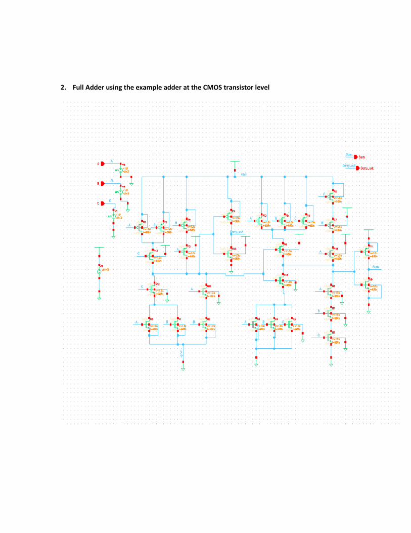
2. Full Adder using the example adder at the CMOS transistor level
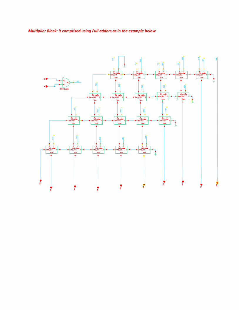
Multiplier Block: it comprised using Full adders as in the example below
Design Project P1
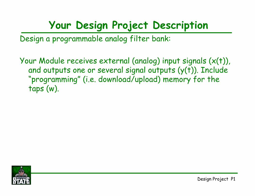
Your Design Project Description Design a programmable analog filter bank:
Your Module receives external (analog) input signals (x(t)), and outputs one or several signal outputs (y(t)). Include “programming” (i.e. download/upload) memory for the taps (w).

Design Project P2ECE 410, Prof. F. Salem
Non-adaptive Filter-Bank Processor .
i
0 0
i
0 0
y=Wx;
or
y : :
y : ( )
j n j n
ij j ij ij ij j
j j
j n j n
ij j ij
j j
w x y y w x
w x w s t jdt
= =
= =
= =
= =
= = ⇒ =
= = −
∑ ∑
∑ ∑
Processor is to compute a vector-matrix multiplication.
Local
computation of
analog
multipliers
(analog) Multiplier cell
For speech/music signal s(t), one may gets:

Design Project P3ECE 410, Prof. F. Salem
Signal lines: Cross-bar (array) layout .
xj
yi
x1
y1

Design Project P4ECE 410, Prof. F. Salem
yi
xj
wij
MU
X
c
Basic Cell
MDAC
Static memory
Floating-gate
Dynamic
memory
1) Choose memory type
to generate the taps (w_ij)
2) Use Trans-amp for an analog
multiplier
3) Connect cell outputs to sum current

Design Project P5ECE 410, Prof. F. Salem
y1
y0
ynx1
x0
xN
δ0
δN
MDAC
Mux
ADC control
wi0
1D
1D1D
MDACw
00x0
e0
w00
vb
1D
1D1D
MDACw
10x0
e1
w10
vb
1D
1D1D
MDACw
n0x0
en
wn0
vb
1D
1D1D
MDACw01
x1
e0
w01
vb
1D
1D1D
MDACw11
x1
e1
w11
vb
1D
1D1D
MDACwn1
x1
en
wn1
vb
1D
1D1D
MDACw0n
xn
e0
w0n
vb
1D
1D1D
MDACw1n
xn
e1
w1n
vb
1D
1D1D
MDACwnn
xn
en
wnn
vb
MDAC
Mux
ADC control
MDAC
Mux
ADC control
Learning/ProcessingADC Control Bus MUX Control Bus
i
win
e1
e0
en
δ1
Basic Cell
Design Project P6ECE 410, Prof. F. Salem
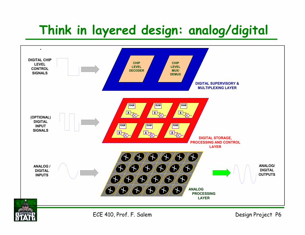
Think in layered design: analog/digital .
X X X X X X
X X X X X X
X X X X X X
X X X X X X
ANALOG /
DIGITAL
INPUTS
ANALOG/
DIGITAL
OUTPUTS
(OPTIONAL)
DIGITAL
INPUT
SIGNALS
DIGITAL CHIP
LEVEL
CONTROL
SIGNALS
ANALOG NEURAL
PROCESSING
LAYER
DIGITAL STORAGE,
PROCESSING AND CONTROL
LAYER
DIGITAL SUPERVISORY &
MULTIPLEXING LAYER
RAM
X
RAM
X
RAM
X
RAM
X
RAM
X
RAM
X
CHIP
LEVEL
DECODER
CHIP
LEVEL
MUX/
DEMUX

Design Project P7ECE 410, Prof. F. Salem
Architectural Design .
The Module design is comprised of three stages
•High Level (“system” specifications, block definitions)
•Component Level (Architectural/topology, simulations)
•Layout Level (Cadence LVS, DRC,..)
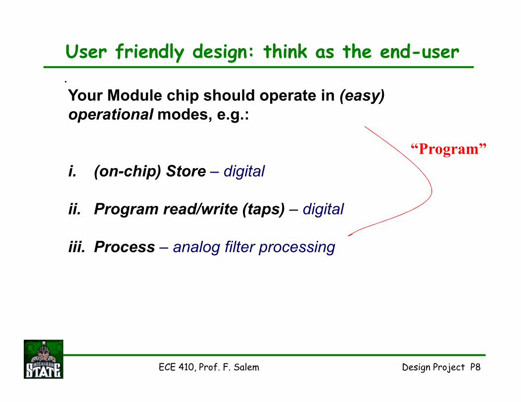
Design Project P8ECE 410, Prof. F. Salem
User friendly design: think as the end-user .
Your Module chip should operate in (easy)
operational modes, e.g.:
i. (on-chip) Store – digital
ii. Program read/write (taps) – digital
iii. Process – analog filter processing
“Program”