
Design of the Photovoltaic Inverter Power Based on TL494
4
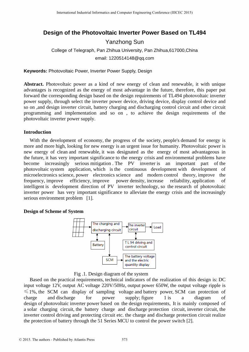
Design of the Photovoltaic Inverter Power Based on TL494 Yanzhong Sun College of Telegraph, Pan Zhihua University, Pan Zhihua,617000,China email: [email protected] Keywords: Photovoltaic Power, Inverter Power Supply, Design Abstract. Photovoltaic power as a kind of new energy of clean and renewable, it with unique advantages is recognized as the energy of most advantage in the future, therefore, this paper put forward the corresponding design based on the design requirements of TL494 photovoltaic inverter power supply, through select the inverter power device, driving device, display control device and so on ,and design inverter circuit, battery charging and discharging control circuit and other circuit programming and implementation and so on , to achieve the design requirements of the photovoltaic inverter power supply. Introduction With the development of economy, the progress of the society, people's demand for energy is more and more high, looking for new energy is an urgent issue for humanity. Photovoltaic power is new energy of clean and renewable, it was designated as the energy of most advantageous in the future, it has very important significance to the energy crisis and environmental problems have become increasingly serious mitigation . The PV inverter is an important part of the photovoltaic system application, which is the continuous development with development of microelectronics science, power electronics science and modern control theory, improve the frequency, improve efficiency, improve power density, increase reliability, application of intelligent is development direction of PV inverter technology, so the research of photovoltaic inverter power has very important significance to alleviate the energy crisis and the increasingly serious environment problem [1]. Design of Scheme of System Fig .1. Design diagram of the system Based on the practical requirements, technical indicators of the realization of this design is: DC input voltage 12V, output AC voltage 220V/50Hz, output power 650W, the output voltage ripple is ≤1%, the SCM can display of sampling voltage and battery power, SCM can protection of charge and discharge for power supply; figure 1 is a diagram of design of photovoltaic inverter power based on the design requirements, It is mainly composed of a solar charging circuit, the battery charge and discharge protection circuit, inverter circuit, the inverter control driving and protecting circuit etc. the charge and discharge protection circuit realize the protection of battery through the 51 Series MCU to control the power switch [2]. International Industrial Informatics and Computer Engineering Conference (IIICEC 2015) © 2015. The authors - Published by Atlantis Press 573
Transcript of Design of the Photovoltaic Inverter Power Based on TL494
Design of the Photovoltaic Inverter Power Based on TL494 Yanzhong Sun
College of Telegraph, Pan Zhihua University, Pan Zhihua,617000,China email: [email protected]
Keywords: Photovoltaic Power, Inverter Power Supply, Design
Abstract. Photovoltaic power as a kind of new energy of clean and renewable, it with unique advantages is recognized as the energy of most advantage in the future, therefore, this paper put forward the corresponding design based on the design requirements of TL494 photovoltaic inverter power supply, through select the inverter power device, driving device, display control device and so on ,and design inverter circuit, battery charging and discharging control circuit and other circuit programming and implementation and so on , to achieve the design requirements of the photovoltaic inverter power supply.
Introduction With the development of economy, the progress of the society, people's demand for energy is
more and more high, looking for new energy is an urgent issue for humanity. Photovoltaic power is new energy of clean and renewable, it was designated as the energy of most advantageous in the future, it has very important significance to the energy crisis and environmental problems have become increasingly serious mitigation . The PV inverter is an important part of the photovoltaic system application, which is the continuous development with development of microelectronics science, power electronics science and modern control theory, improve the frequency, improve efficiency, improve power density, increase reliability, application of intelligent is development direction of PV inverter technology, so the research of photovoltaic inverter power has very important significance to alleviate the energy crisis and the increasingly serious environment problem [1].
Design of Scheme of System
Fig .1. Design diagram of the system Based on the practical requirements, technical indicators of the realization of this design is: DC
input voltage 12V, output AC voltage 220V/50Hz, output power 650W, the output voltage ripple is≤1%, the SCM can display of sampling voltage and battery power, SCM can protection of charge and discharge for power supply; figure 1 is a diagram of design of photovoltaic inverter power based on the design requirements, It is mainly composed of a solar charging circuit, the battery charge and discharge protection circuit, inverter circuit, the inverter control driving and protecting circuit etc. the charge and discharge protection circuit realize the protection of battery through the 51 Series MCU to control the power switch [2].
International Industrial Informatics and Computer Engineering Conference (IIICEC 2015)
© 2015. The authors - Published by Atlantis Press 573
Design of Hardware Circuit of System Selection of inverter power devices is to achieve efficient conditions, when the power
switch selection, it should consider the breakdown voltage, encapsulation, thermal (from junction to case), parasitic capacitance, conductive voltage ,current rating, conductor resistance , switching speed , cost and other factors , since the MOSFET IRF3205 with advanced manufacturing technology, low conductor resistance , high slew rate, durable and so on, so as the preferred devices in this design [2].
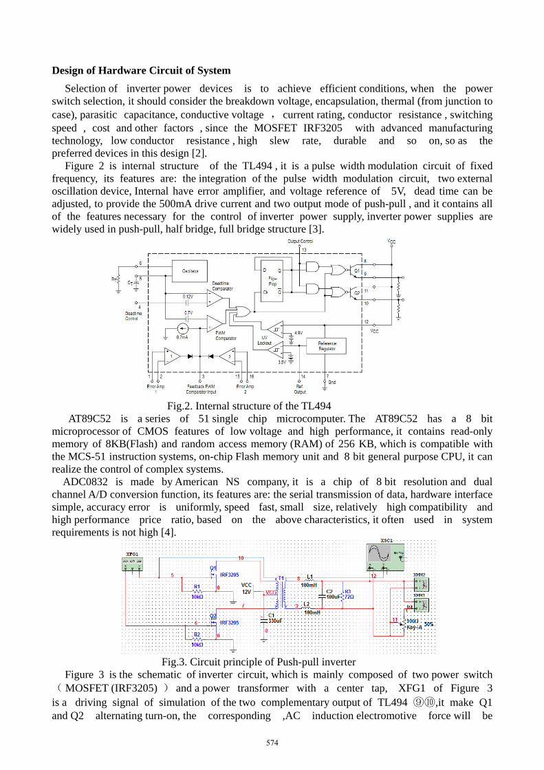
Figure 2 is internal structure of the TL494 , it is a pulse width modulation circuit of fixed frequency, its features are: the integration of the pulse width modulation circuit, two external oscillation device, Internal have error amplifier, and voltage reference of 5V, dead time can be adjusted, to provide the 500mA drive current and two output mode of push-pull , and it contains all of the features necessary for the control of inverter power supply, inverter power supplies are widely used in push-pull, half bridge, full bridge structure [3].
Fig.2. Internal structure of the TL494 AT89C52 is a series of 51 single chip microcomputer. The AT89C52 has a 8 bit
microprocessor of CMOS features of low voltage and high performance, it contains read-only memory of 8KB(Flash) and random access memory (RAM) of 256 KB, which is compatible with the MCS-51 instruction systems, on-chip Flash memory unit and 8 bit general purpose CPU, it can realize the control of complex systems.
ADC0832 is made by American NS company, it is a chip of 8 bit resolution and dual channel A/D conversion function, its features are: the serial transmission of data, hardware interface simple, accuracy error is uniformly, speed fast, small size, relatively high compatibility and high performance price ratio, based on the above characteristics, it often used in system requirements is not high [4].
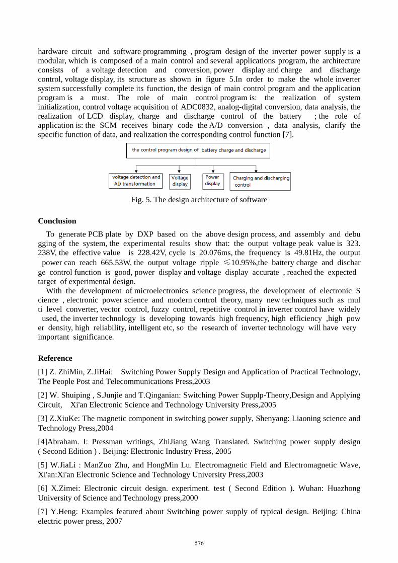
Fig.3. Circuit principle of Push-pull inverter
Figure 3 is the schematic of inverter circuit, which is mainly composed of two power switch ( MOSFET (IRF3205) ) and a power transformer with a center tap, XFG1 of Figure 3 is a driving signal of simulation of the two complementary output of TL494 ⑨⑩,it make Q1 and Q2 alternating turn-on, the corresponding ,AC induction electromotive force will be
574

generated in the secondary coil of T1 transformer. Although the voltage of the primary output is square wave, but the output of the LC filter circuit composed of L1, L2 and C2 of the secondary is the sine wave, and then sent to the load [5].
In Figure 3, the transformer is a kind of magnetic components, it mainly is composed of the iron core and the coil winding, and the power transformer is a device to transfer 50Hz AC power, it also has the effect of isolating and transformer, its output voltage and input voltage ratio is equal to the secondary turns and primary turns ratio. in this design Because the input voltage U1 is 12V, the peak is output voltage is 308V, the ratio of the number of turns of the coil is 0.0375, then get the output waveform of the inverter circuit as shown in figure 4.
Fig. 4: The output waveform of push-pull inverter circuit
Lithium battery as important energy storage component of photovoltaic power generation, requirements is very strict on the charger, in order to prevent overcharge and over discharge of the battery , it needs protection circuit, Figure 5 is a protection and display control circuit of inverter power, which is mainly composed of a main control circuit, A/D conversion circuit, a voltage display circuit, a power display circuit, charging and discharging control switch circuit etc.. The main control circuit uses the AT89C52 microcontroller, A/D conversion selects voltage ADC0832 chip, display voltage selected liquid crystal display of the LCD1206, The control switch circuit charge and discharge selects MOSFET switch, power display using five LED lamps. its working principle as following: when the sensor acquisition voltage of the battery is transmitted to A/D converter, ADC0832 will sensor voltage and the reference voltage comparison, the formation of 8bit serial data output to the SCM, SCM will operation and processing, the battery voltage is displayed in the LCD, at the same time, SCM will analysis voltage, when the voltage value is higher than the saturation voltage of the battery, SCM will switched off charge circuit, and avoid over charging [6] .
Fig.5. control circuit diagram of protection and display
When the detected voltage is lower than the minimum voltage of the battery, the MCU will switched off discharge circuit, and avoid excessive discharge of the battery, so as to realize the protection of the battery, at the same time in order to intuitively understand power of the battery, this with five LED lights to display battery power, when the battery voltage is less than 11V, an LED lamp; when the voltage of the battery is 11V~11.5V, two LED lights; when the voltage of the battery is 11.5V~12V, three LED lights; when the voltage of the battery is 12V~12.5V, four LED lights lit, when the battery voltage is more than 12.5V, all LED lights were lit, so use voltage changes implemented detection of battery.
The Design of Software Design of battery charging and discharging circuit mainly includes two aspects: the design of the
575
hardware circuit and software programming , program design of the inverter power supply is a modular, which is composed of a main control and several applications program, the architecture consists of a voltage detection and conversion, power display and charge and discharge control, voltage display, its structure as shown in figure 5.In order to make the whole inverter system successfully complete its function, the design of main control program and the application program is a must. The role of main control program is: the realization of system initialization, control voltage acquisition of ADC0832, analog-digital conversion, data analysis, the realization of LCD display, charge and discharge control of the battery ; the role of application is: the SCM receives binary code the A/D conversion , data analysis, clarify the specific function of data, and realization the corresponding control function [7].
Fig. 5. The design architecture of software
Conclusion To generate PCB plate by DXP based on the above design process, and assembly and debu
gging of the system, the experimental results show that: the output voltage peak value is 323.238V, the effective value is 228.42V, cycle is 20.076ms, the frequency is 49.81Hz, the output power can reach 665.53W, the output voltage ripple ≤10.95%,the battery charge and discharge control function is good, power display and voltage display accurate , reached the expected target of experimental design.
With the development of microelectronics science progress, the development of electronic Science , electronic power science and modern control theory, many new techniques such as multi level converter, vector control, fuzzy control, repetitive control in inverter control have widely used, the inverter technology is developing towards high frequency, high efficiency ,high power density, high reliability, intelligent etc, so the research of inverter technology will have very important significance.
Reference
[1] Z. ZhiMin, Z.JiHai: Switching Power Supply Design and Application of Practical Technology, The People Post and Telecommunications Press,2003
[2] W. Shuiping , S.Junjie and T.Qinganian: Switching Power Supplp-Theory,Design and Applying Circuit, Xi'an Electronic Science and Technology University Press,2005
[3] Z.XiuKe: The magnetic component in switching power supply, Shenyang: Liaoning science and Technology Press,2004
[4]Abraham. I: Pressman writings, ZhiJiang Wang Translated. Switching power supply design ( Second Edition ) . Beijing: Electronic Industry Press, 2005
[5] W.JiaLi : ManZuo Zhu, and HongMin Lu. Electromagnetic Field and Electromagnetic Wave, Xi'an:Xi'an Electronic Science and Technology University Press,2003
[6] X.Zimei: Electronic circuit design. experiment. test ( Second Edition ). Wuhan: Huazhong University of Science and Technology press,2000
[7] Y.Heng: Examples featured about Switching power supply of typical design. Beijing: China electric power press, 2007
576