Design of Robust and power Efficient 8-Bit Ripple Carry ... · Ripple Carry Adder using Different...
7
SSRG International Journal of VLSI & Signal Processing (SSRG-IJVSP) – volume 3 Issue 2 May to Aug 2016 ISSN: 2394 - 2584 www.internationaljournalssrg.org Page 1 Design of Robust and power Efficient 8-Bit Ripple Carry Adder using Different Logic Styles Mangayarkkarasi M 1 , Joseph Gladwin S 2 1 Assistant Professor, 2 Associate Professor 12 Department of ECE 1 Sri Muthukumaran Institute of Technology, 2 SSN College of Engineering, 12 India. Abstract—The binary adders are key component in digital signal processors (DSP). These adders are crucial building blocks in very large scale integrated circuits. Its efficient implementation is highly important because a carry propagation involving all operand bits has to be performed. With the increasing level of device integration power became the predominant design goal for fast adders. Low power consumption and smaller area are some of the most important criteria for fabrication of DSP systems and high performance systems. In this paper we try to determine the best solution to this problem by comparing a few 8-bit Ripple Carry Adder (RCA) circuits implementation with Complementary, Dynamic, Constant Delay (CD) and Energy Efficient Constanta Delay (EE-CD) logic styles. The adders are simulated using MicroWind environment to find an efficient adder structure. To reduce the power consumption for low power applications an EE- CD logic style is proposed. When we compare the power consumption of all the adder logic style we find that Complementary logic style consume more power. The EE-CD logic style has better power consumption compared to all other logic styles. Keywords—CMOS, Ripple Carry Adder, Power Consumption, Complementary Logic, Dynamic Logic, Constant Delay Logic, Energy Efficient- Constant Delay Logic. I. INTRODUCTION To add the data in the processor adders are most widely used[1]. A significant performance improvement in integrated circuits are scaling of the transistor size and reduction in power. There are two most important factors to realizing modern VLSI circuits are low-power and high-speed. In VLSI circuits the high performance energy efficient logic styles are always important. To construct these types of integrated circuits CMOS technology is the most commonly used. Power parameter is most widely used to measure the quality of the circuits. The advancement in the CMOS technology leads to improve the power [2]. To enhance the speed of the digital circuitry (Dynamic Logic) many improvements has been done [3]. But this logic is affected by charge leakage, charge sharing and backgate coupling of logic blocks. To avoid this problem, the CMOS domino logic (Feedthrough) was introduced [4]. Before all the inputs are valid, the output is partially evaluated. This is the most important feature of domino logic; it‟s also occurs due to extra supply. The architecture, logic style, layout and process technology are the different levels of high- performance and low-power adders. To optimize the speed in adders, we need carry generation. For fast adder implementation, the generated carry should convey to the output as soon as possible. So the worst path delay which determines the speed of the digital processor can be reduced. We can obtain the Ripple Carry Adder (RCA) by cascading many single-bit Full Adder (FA)cells[5]. This architecture is simple and area efficient. Each FA starts operation till the previous carry out signal is ready which is shown in Fig. 1. Because of this effect the computation speed is slow. This adder is very fast in operation compared to other high-speed adders. The path delay is determined by its carry out propagation route. The number of bits increases, the delay of RCA increases in a linear way. The equation 1 describes the delay of RCA. The Boolean expressions for Sum and Carry are given in equation 2 and 3. The corresponding truth table shown in Table 1. TABLE I TRUTH TABLE OF ONE-BIT FULL ADDER
Transcript of Design of Robust and power Efficient 8-Bit Ripple Carry ... · Ripple Carry Adder using Different...

SSRG International Journal of VLSI & Signal Processing (SSRG-IJVSP) – volume 3 Issue 2 May to Aug 2016
ISSN: 2394 - 2584 www.internationaljournalssrg.org Page 1
Design of Robust and power Efficient 8-Bit
Ripple Carry Adder using Different Logic
Styles Mangayarkkarasi M
1, Joseph Gladwin S
2
1Assistant Professor,
2Associate Professor
12Department of ECE
1Sri Muthukumaran Institute of Technology,
2SSN College of Engineering,
12India.
Abstract—The binary adders are key
component in digital signal processors (DSP).
These adders are crucial building blocks in very
large scale integrated circuits. Its efficient
implementation is highly important because a
carry propagation involving all operand bits has
to be performed. With the increasing level of
device integration power became the
predominant design goal for fast adders. Low
power consumption and smaller area are some
of the most important criteria for fabrication of
DSP systems and high performance systems. In
this paper we try to determine the best solution
to this problem by comparing a few 8-bit Ripple
Carry Adder (RCA) circuits implementation with
Complementary, Dynamic, Constant Delay (CD)
and Energy Efficient Constanta Delay (EE-CD)
logic styles. The adders are simulated using
MicroWind environment to find an efficient
adder structure. To reduce the power
consumption for low power applications an EE-
CD logic style is proposed. When we compare
the power consumption of all the adder logic
style we find that Complementary logic style
consume more power. The EE-CD logic style has
better power consumption compared to all other
logic styles.
Keywords—CMOS, Ripple Carry Adder, Power
Consumption, Complementary Logic, Dynamic Logic,
Constant Delay Logic, Energy Efficient- Constant
Delay Logic.
I. INTRODUCTION
To add the data in the processor adders are most
widely used[1]. A significant performance
improvement in integrated circuits are scaling of
the transistor size and reduction in power. There
are two most important factors to realizing modern
VLSI circuits are low-power and high-speed.
In VLSI circuits the high performance energy
efficient logic styles are always important. To
construct these types of integrated circuits CMOS
technology is the most commonly used. Power
parameter is most widely used to measure the
quality of the circuits. The advancement in the
CMOS technology leads to improve the power [2].
To enhance the speed of the digital circuitry
(Dynamic Logic) many improvements has been
done [3]. But this logic is affected by charge
leakage, charge sharing and backgate coupling of
logic blocks. To avoid this problem, the CMOS
domino logic (Feedthrough) was introduced [4].
Before all the inputs are valid, the output is
partially evaluated. This is the most important
feature of domino logic; it‟s also occurs due to
extra supply.
The architecture, logic style, layout and process
technology are the different levels of high-
performance and low-power adders. To optimize
the speed in adders, we need carry generation. For
fast adder implementation, the generated carry
should convey to the output as soon as possible. So
the worst path delay which determines the speed of
the digital processor can be reduced.
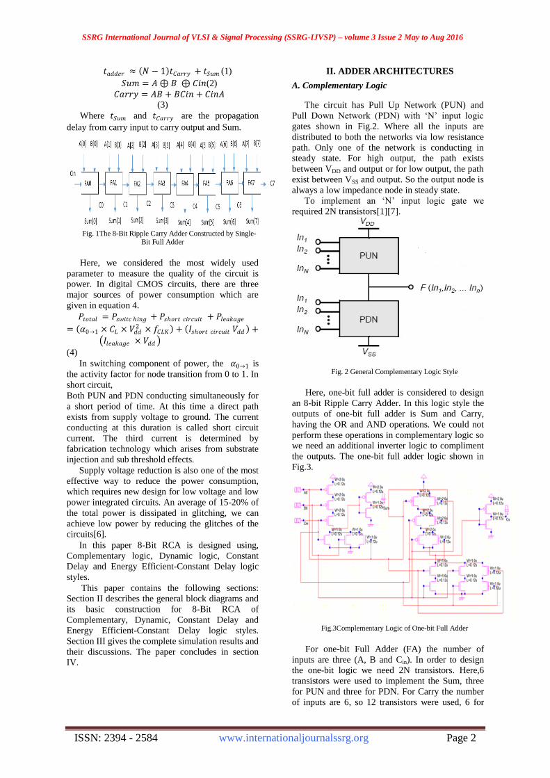
We can obtain the Ripple Carry Adder (RCA) by
cascading many single-bit Full Adder (FA)cells[5].
This architecture is simple and area efficient. Each
FA starts operation till the previous carry out signal
is ready which is shown in Fig. 1. Because of this
effect the computation speed is slow. This adder is
very fast in operation compared to other high-speed
adders.
The path delay is determined by its carry out
propagation route. The number of bits increases, the
delay of RCA increases in a linear way. The
equation 1 describes the delay of RCA. The
Boolean expressions for Sum and Carry are given in
equation 2 and 3. The corresponding truth table
shown in Table 1.
TABLE I
TRUTH TABLE OF ONE-BIT FULL ADDER
SSRG International Journal of VLSI & Signal Processing (SSRG-IJVSP) – volume 3 Issue 2 May to Aug 2016
ISSN: 2394 - 2584 www.internationaljournalssrg.org Page 2
𝑡𝑎𝑑𝑑𝑒𝑟 ≈ 𝑁 − 1 𝑡𝐶𝑎𝑟𝑟𝑦 + 𝑡𝑆𝑢𝑚 (1)
𝑆𝑢𝑚 = 𝐴 ⊕ 𝐵 ⊕ 𝐶𝑖𝑛(2)
𝐶𝑎𝑟𝑟𝑦 = 𝐴𝐵 + 𝐵𝐶𝑖𝑛 + 𝐶𝑖𝑛𝐴 (3)
Where 𝑡𝑆𝑢𝑚 and 𝑡𝐶𝑎𝑟𝑟𝑦 are the propagation
delay from carry input to carry output and Sum.
Fig. 1The 8-Bit Ripple Carry Adder Constructed by Single-
Bit Full Adder
Here, we considered the most widely used
parameter to measure the quality of the circuit is
power. In digital CMOS circuits, there are three
major sources of power consumption which are
given in equation 4.
𝑃𝑡𝑜𝑡𝑎𝑙 = 𝑃𝑠𝑤𝑖𝑡𝑐 𝑖𝑛𝑔 + 𝑃𝑠𝑜𝑟𝑡 𝑐𝑖𝑟𝑐𝑢𝑖𝑡 + 𝑃𝑙𝑒𝑎𝑘𝑎𝑔𝑒
= 𝛼0→1 × 𝐶𝐿 × 𝑉𝑑𝑑2 × 𝑓𝐶𝐿𝐾 + 𝐼𝑠𝑜𝑟𝑡 𝑐𝑖𝑟𝑐𝑢𝑖𝑡 𝑉𝑑𝑑 +
𝐼𝑙𝑒𝑎𝑘𝑎𝑔𝑒 × 𝑉𝑑𝑑
(4)
In switching component of power, the 𝛼0→1 is
the activity factor for node transition from 0 to 1. In
short circuit,
Both PUN and PDN conducting simultaneously for
a short period of time. At this time a direct path
exists from supply voltage to ground. The current
conducting at this duration is called short circuit
current. The third current is determined by
fabrication technology which arises from substrate
injection and sub threshold effects.
Supply voltage reduction is also one of the most
effective way to reduce the power consumption,
which requires new design for low voltage and low
power integrated circuits. An average of 15-20% of
the total power is dissipated in glitching, we can
achieve low power by reducing the glitches of the
circuits[6].
In this paper 8-Bit RCA is designed using,
Complementary logic, Dynamic logic, Constant
Delay and Energy Efficient-Constant Delay logic
styles.
This paper contains the following sections:
Section II describes the general block diagrams and
its basic construction for 8-Bit RCA of
Complementary, Dynamic, Constant Delay and
Energy Efficient-Constant Delay logic styles.
Section III gives the complete simulation results and
their discussions. The paper concludes in section
IV.
II. ADDER ARCHITECTURES
A. Complementary Logic
The circuit has Pull Up Network (PUN) and
Pull Down Network (PDN) with „N‟ input logic
gates shown in Fig.2. Where all the inputs are
distributed to both the networks via low resistance
path. Only one of the network is conducting in
steady state. For high output, the path exists
between VDD and output or for low output, the path
exist between VSS and output. So the output node is
always a low impedance node in steady state.
To implement an „N‟ input logic gate we
required 2N transistors[1][7].
Fig. 2 General Complementary Logic Style
Here, one-bit full adder is considered to design
an 8-bit Ripple Carry Adder. In this logic style the
outputs of one-bit full adder is Sum and Carry,
having the OR and AND operations. We could not
perform these operations in complementary logic so
we need an additional inverter logic to compliment
the outputs. The one-bit full adder logic shown in
Fig.3.
Fig.3Complementary Logic of One-bit Full Adder
For one-bit Full Adder (FA) the number of
inputs are three (A, B and Cin). In order to design
the one-bit logic we need 2N transistors. Here,6
transistors were used to implement the Sum, three
for PUN and three for PDN. For Carry the number
of inputs are 6, so 12 transistors were used, 6 for
SSRG International Journal of VLSI & Signal Processing (SSRG-IJVSP) – volume 3 Issue 2 May to Aug 2016
ISSN: 2394 - 2584 www.internationaljournalssrg.org Page 3
PUN and 6 for PDN. An CMOS inverter is added
additionally to both the outputs.
Here, the 8-bit RCA implemented using the
above one-bit complementary logic style, which is
shown in Fig. 4. The total number of transistors
used here is 178. For each Sum 6 transistors are
used with a CMOS inverter. With addition to
CMOS inverter 12 transistor used for each Carry.
Fig.4 8-Bit RCA using Complementary Logic Style
In this logic the carry output of the first stage
FA (C0) is given to the carry input of the second
stage FA. This process continued till we get the
carry output (C7) of the 8th
stage. The Sum outputs
are Sum0 to Sum7.
B. Dynamic Logic
Fig.5General Dynamic Logic Style
The circuit requires 2+N transistors to
implement the logic function which is shown in
Fig.5. The additional two transistors are used for
precharge and evaluation phases to realize the logic
functions. When the clock signal (ф) is low, the
evaluation transistor (Me) is OFF and there is no
static power. The precharge transistor (Mp) is OFF
when the clock signal (ф) is high. The output of a
dynamic gate is once discharged; it cannot be
charged again until the next precharge operation.
During evaluation the inputs to the gate makes at
most one transition. During and after evaluation the
output should be in high impedance state and it‟s
stored on CL. The dynamic circuits having the
following properties: The logic function is
implemented by the PDN only, Full scaling outputs,
Non-Ratioed, Faster switching speed and Needs a
precharge/evaluation clocks[1][7-8].
Here, we are using only PDN with the addition
of precharge (Mp) and evaluation (Me) transistors.
To construct the one-bit Dynamic logic using FA
we need N+2 transistors. So 3 transistors used for
Sum and 6 transistors for Carry with precharge and
evaluation transistors. The dynamic logic shown in
Fig.6. The CMOS inverters in the output stage is
eliminated here.
Fig. 6 Dynamic Logic of One-bit Full Adder
Here, the 8-bit RCA implemented using the
above one-bit Dynamic logic style, which is shown
in Fig.7. The total number of transistors used here is
104. For each Sum 3 transistors are used with a
precharge and evaluation transistors (Mp and Me).
With addition to precharge and evaluation
transistors 6 transistor used for each Carry. The
charging and discharging done through the
capacitor (CL).
Fig. 7 8-Bit RCA using Dynamic Logic Style

SSRG International Journal of VLSI & Signal Processing (SSRG-IJVSP) – volume 3 Issue 2 May to Aug 2016
ISSN: 2394 - 2584 www.internationaljournalssrg.org Page 4
C. Constant Delay (CD) Logic
In this logic the static power is reduced by
using a Timing Block(TB) which creates an
adjustable window period. The general logic and its
timing diagram‟s shown in Fig.8 and 9.
Fig.8 General Constant Delay (CD) Logic Style
Fig.9 Timing Diagram of Constant Delay (CD) Logic
Style
When CLK is high, both X and Y are pre-
discharged to GND. When CLK is low, the CD
Logic enters into evaluation period. This period
consists of three cases Contention, C-Q delay and
D-Q delay modes[9-10].
1. Contention Mode
When the CLK is low: IN (inputs of PDN)
remains at logic “1” and X is in a non-zero voltage
level which leads the Out to a temporary glitch.
The window width determines this duration, which
is determined by the delay occurs between CLK
and CLK_d.
When the CLK_d is high: X remains at low and
Y raised to logic “1”, which turns OFF M1. At this
time the period is over and the temporary glitch in
the Out is eliminated.
2. C-Q Delay Mode
This mode occurs before the CLK becomes low
with IN (inputs of PDN) make a transition from
high to low. For the entire evaluation period, X
raises to logic “1” and Y remains at logic “0”,
when CLK becomes low.
3. D-Q Delay Mode
To enable the high performance operations this
mode utilizes the pre-evaluated characteristics of
CD logic. Before the IN (inputs of PDN) transit
CLK falls from high to low and X is initially rises
to a non-zero voltage level. The Y is still low but
IN (inputs of PDN) become logic “0” and X
quickly rises to logic “1”. When the CLK_d rises
little slower than X, then Y will initially rise but
return back to logic “0”.
Fig.10Constant Delay (CD) Logic of One-bit Full Adder
Here, we are using only PDN with the addition
of Timing Block and Logic Block. To construct the
one-bit Constant Delay logic using FA we need
N+3 transistors with TB and Logic Block. So 3
transistors used for Sum and 6 transistors for Carry
with additional 3 transistors (M0, M1 and M2). The
CD logic shown in Figure 10.
Fig.11 8-Bit RCA using Constant Delay (CD) Logic Style
In this logic the total number of transistors used
here is 88. For each Sum 4 transistors are used with
aninverter and 7 transistor used for each Carry with
the addition to an inverter. Here we can keep the
structure up to X logic for all stages. The X logic
having TB with transistors M0 and M1. So totally 94

SSRG International Journal of VLSI & Signal Processing (SSRG-IJVSP) – volume 3 Issue 2 May to Aug 2016
ISSN: 2394 - 2584 www.internationaljournalssrg.org Page 5
transistors were used in this logic which is shown in
Figure 11.
D. Energy Efficient-Constant Delay (EE-CD)
Logic
The EE-CD logic reduces the power
consumption by control the PUN through feedback
technique shown in Fig. 12. The PUN having the
transistor (T3) in series with transistor (T1) and T3
transistor is controlled by the drain of the T2
transistor. The inverted CLK signal drives the
source of transistor T2 and the output signal is taken
to control the gate terminal of transistor T2. When
the CLK signal is high the T4 transistor reset the
node X. The transistor T6 is used to reset the output
terminal. PDN consist only NMOS transistors.
Fig.12 General Energy Efficient-Constant Delay (EE-CD)
Logic Style
The EE-CD logic having two modes of
operation, reset and evaluation mode [11-13].
1. Reset Mode
When CLK is high both X and OUT pre-
discharges to GND, so the output always at
logic “0”.
2. Evaluation Mode
When CLK is low the circuit enters into
the evaluation mode, here contention mode takes
place. In this mode, the CLK is low when the input
(IN) at logic “1”. At this time both PUN and PDN
conduct simultaneously, which causes a temporary
glitch at the output. So it creates a direct path
between power supply and ground. The output node
become a non-zero voltage level is used to turn ON
the transistor T2 by feedback method. The inverted
CLK pass through transistor T2 is disables the
transistor T3. So the direct path is disabled till the
entire contention period and the glitches has been
eliminated.
The EE-CD logic shown in Fig. 13. Here, we are
using PUN as X Logic. To construct the one-bit EE-
CD logic using FA we need N+1 transistors with X
Logic. The X logic having transistors T1, T2 and T3
with additional transistor T4 used to reset the logic.
So 3 transistors used for Sum and 6 transistors for
Carry with additional transistor used to reset the
output terminal.
Fig. 13 Energy Efficient-Constant Delay (EE-CD) Logic of
One-bit Full Adder
Fig.148-Bit RCA using Energy Efficient-Constant Delay
(CD) Logic Style
In this logic the total number of transistors used
here is 88. For each Sum 4 transistors are used with
an X Logic. Here we can keep the structure up to X
Logic for all stages. The X logic having the
transistors T1, T2, T3 with additional reset transistor
T3. So totally 92 transistors were used in this logic
which is shown in Fig. 14.
III. SIMULATION RESULTS FOR POWER
ANALYSIS OF DIFFERENT 8-BIT RCA
LOGIC STYLES
The Fig. 15-18. below describe the output
waveforms of 8-Bit RCA using complementary,
Dynamic, Constant Delay and Energy Efficient-
Constant Delay logic styles.

SSRG International Journal of VLSI & Signal Processing (SSRG-IJVSP) – volume 3 Issue 2 May to Aug 2016
ISSN: 2394 - 2584 www.internationaljournalssrg.org Page 6
Fig.15 Simulation Waveform of 8-Bit RCA Using
Complementary Logic Style with Power
The truth table was verified by the simulation
waveform which is shown in Fig. 15. using the
complementary logic style.
Fig. 16 SimulationWaveform of 8-Bit RCA Using Dynamic
Logic Style with Power
The operation of the 8-Bit Dynamic logic has
been verified by the truth table with common clock
signal which is shown in Fig. 16. Whenever the
clock signal is low, all the evaluation transistors are
OFF and also there is no static power consumption
and its vice-versa for precharge phase. During and
after evaluation all the inputs must have one
transition.
Fig. 17 SimulationWaveform of 8-Bit RCA Using Constant
Delay Logic Style with Power
The Fig. 17. verifies the adder logic with
precharge and evaluation phases using common
clock signal and common timing block for all
stages. The three modes, contention mode, C-D
delay mode and D-Q delay modes of evaluation
phase also verified.
Fig. 18 SimulationWaveform of 8-Bit RCA Using Energy
Efficient-Constant Delay Logic Style with Power
When the clock signal is high and the outputs
are always at high during the Reset mode. The
contention mode takes place during the evaluation
phase. At this time the clock signal is low and
inputs are in logic “1”. So both PUN and PDN
conduct simultaneously and glitches occurred at this
phase. By disabling the direct path in entire
contention period the glitches eliminated which is
also shown in Fig. 18.

SSRG International Journal of VLSI & Signal Processing (SSRG-IJVSP) – volume 3 Issue 2 May to Aug 2016
ISSN: 2394 - 2584 www.internationaljournalssrg.org Page 7
TABLE II POWER ANALYSIS OF FOR POWER ANALYSIS
OF DIFFERENT 8-BIT RCA LOGIC STYLES
Logic Style Number of
Transistors
Power
(μW)
Complementary 176 68.819
Dynamic 104 44.517
Constant Delay 94 18.011
Energy Efficient Constant
Delay
92 4.770
The power consumption is calculated by using
the different values of width of the transistors. If the
width is minimum, we can calculate how much
power consumed. The overall power is the
combination of short circuit and switching power.
The dynamic energy consumption consumed energy
of power supply during Sum and Carry operations.
The above Table IIshows the number of transistors
and power calculations of different logic styles.
IV.CONCLUSION
In this paper, different types of 8-Bit Ripple
Carry Adders (Complementary, Dynamic, Constant
Delay and Energy Efficient-Constant Delay) has
been designed and evaluated on power parameter.
Both constant Delay and Energy Efficient-Constant
Delay adders uses least number of transistors while
complementary logic has highest number of
transistors i.e. 176 transistors. Compared to this the
Dynamic logic has moderate number of transistors.
The Complementary logic has highest power of
68.819μW compared to other logic styles. Dynamic
logic has the power of 44.517μW which is better
than complementary and higher than other two logic
styles. By observing the powers of Constant Delay
and Energy Efficient-Constant Delay logics, it is
observed that Energy Efficient-Constant Delay
logic has a superior power of 4.770μW than
18.011μW of Constant Delay logic. Here, we
conclude that power consumption of Efficient-
Constant Delay logic is very less, so it will be
considered as a fast adder.
ACKNOWLEDGMENT
The authors would like to thank the anonymous
reviewers for their careful revision and important
suggestions which significantly helped to improve
the presentation of this paper.
REFERENCES
1. J. M. Rabey, Digital Integrated Circuits, A Design
Perspective. Prentice-Hall, 1996.
2. Deepika Gupta, Nitin Tiwari , Sarin. R.K, “Analysis Of
Modified Feedthrough Logic With Improved Power Delay
Product”, International Journal Of Computer Applications
ISSN : 0975- 8887, vol.69, no.5 pp.214-219, 2013.
3. S. M. Kang, Y. Leblebici, „CMOS Digital Integrated
Circuits: Analysis & Design‟, TATA McGraw- Hill
Publication, 3e, 2003.
4. V. Navarro-Botello, J. A. Montiel-Nelson, and S.
Nooshabadi, “Performance Analysis of high performance
fast feedthrough logic families in CMOS,” IEEE Trans.
Cir. & syst. II, vol. 54, no. 6, Jun. 2007, pp. 489-493.
5. B. Vijayarani, “Design of synchronous full adder”,
International Conference on Computing and Control
Engineering, April 2012.
6. H. Bui, Y. Wang, Y. Jiang, “Design and analysis of low-
power 10-transistor full adders using novel xor–xnor
gates”, IEEE transactions on circuits and systems analog
and digital signal processing, vol. 49, pp. 25-30, 2002.
7. Rajaneesh Sharma and ShekharVerma, “Comparitive
Analysis of Static and Dynamic CMOS Logic Design”,
IEEE International Conference on Computing &
Communication Technologies (ICACCT) , pp.231-234,
2011.
8. Chuang.P, Li.D, and Sachdev.M, “Design of a 64-bit low-
energy high performance adder using dynamic feed
through logic,” in Proc. IEEE Int. Circuits Syst. Symp, pp.
3038–3041, May 2009.
9. Pierce Chuang, David Li, ManojSachdev,“Constant Delay
Logic Style”, IEEE Transactions on Very Large Scale
Integration(VLSI) Systems, vol.21, no.3, pp. 554-565,
2013.
10. K. Lavanya, V. SurendraBabu, “Design of 8-bit Ripple
Carry Adder Using Constant Delay Logic”, International
Journal of Electrical, Electronics and Computer Systems
(IJEECS), vol.2, no.8,9, pp. 32-37, 2014.
11. M. Aguirre-Hernandez and M. Linares-Aranda, “CMOS
CMOS Full-adders for energy-efficient arithmetic
applications,” IEEE Trans. Very Large Scale Integr.
(VLSI) Syst., vol. 19, no. 99, pp. 1–5, Apr. 2010.
12. Arunraj R, Vishnu Narayanan P M, “Design of Robust and
Power Efficient Full Adder Using Energy Efficient
Feedthrough Logic”, International Journal of Engineering
Research and General Science,vol.2, no.2, pp. 96-101,
Feb-Mar 2014.
13. N. Akilandeswari, R. Vijayabhasker, “Design of an
Energy-Efficient Constant Delay Logic for Low Power
Applications”, International Journal of Research and
Innovation in Engineering Technology, vol.1, no.1, pp. 25-
32,June 2014.


![M05 arith1.ppt [호환 모드] · 2016-10-31 · Ripple Carry Adder-4-bit ripple carry adder-LSB에서발생된carry가MSB까지전파된후에야sum 계산완료-Carry의전파가adder의계산시간결정](https://static.fdocuments.in/doc/165x107/5e6dfaba8472c611153db48f/m05-eeoe-2016-10-31-ripple-carry-adder-4-bit-ripple-carry-adder-lsboeeoefeoecarryemsbeoeoeoeeoesum.jpg)