DESIGN OF PRINTED TRACE DIFFERENTIAL OOP … · It is quite normal for an initial fabricated...
28
Rev. 0.1 1/15 Copyright © 2015 by Silicon Laboratories AN639 AN639 D ESIGN OF P RINTED T RACE D IFFERENTIAL L OOP A NTENNAS 1. Introduction This application note discusses the general principles involved with designing a printed circuit trace differential loop antenna, suitable for use with sub-GHz RFICs, such as the Si4010/Si4012 from Silicon Labs. This application note also provides a general tutorial on how to design a differential loop antenna, using a combination of design equations and simulation techniques. Use of loop antennas in small radio devices is often desirable for several reasons. Many modern RFICs use differential circuitry to achieve better performance and provide rejection against common-mode signals; the inherent differential structure of a loop antenna interfaces well to such circuitry. Loop antennas are primarily H-field radiators (compared with E-field radiators, such as monopole antennas) and are somewhat less susceptible to de- tuning because of hand or body effect. Loop antennas may easily be designed using printed circuit traces, allowing a reduction in Bill of Material (BOM) cost. They may also be designed with a relatively small physical size, allowing integration in a very small form factor. However, designing a loop antenna (or any antenna) is not the simplest of tasks. It would be convenient to simply select an antenna design from a proven library of existing designs, or to construct an antenna from a template design and then further scale the dimensions to the desired frequency of operation. In practice, however, it is rarely possible for a designer to copy an existing antenna design exactly, without any modification; it is generally necessary to change the antenna layout (at least slightly) to fit within the user’s form factor. Even such minor modifications can result in changes in the performance of the antenna. Thus, new antenna designs generally require simulation and/or bench adjustment, unless they are exact replicas of existing designs.
Transcript of DESIGN OF PRINTED TRACE DIFFERENTIAL OOP … · It is quite normal for an initial fabricated...

Rev. 0.1 1/15 Copyright © 2015 by Silicon Laboratories AN639
AN639
DESIGN OF PRINTED TRACE DIFFERENTIAL LOOP ANTENNAS
1. IntroductionThis application note discusses the general principles involved with designing a printed circuit trace differential loopantenna, suitable for use with sub-GHz RFICs, such as the Si4010/Si4012 from Silicon Labs. This application notealso provides a general tutorial on how to design a differential loop antenna, using a combination of designequations and simulation techniques.
Use of loop antennas in small radio devices is often desirable for several reasons. Many modern RFICs usedifferential circuitry to achieve better performance and provide rejection against common-mode signals; theinherent differential structure of a loop antenna interfaces well to such circuitry. Loop antennas are primarily H-fieldradiators (compared with E-field radiators, such as monopole antennas) and are somewhat less susceptible to de-tuning because of hand or body effect. Loop antennas may easily be designed using printed circuit traces, allowinga reduction in Bill of Material (BOM) cost. They may also be designed with a relatively small physical size, allowingintegration in a very small form factor.
However, designing a loop antenna (or any antenna) is not the simplest of tasks. It would be convenient to simplyselect an antenna design from a proven library of existing designs, or to construct an antenna from a templatedesign and then further scale the dimensions to the desired frequency of operation. In practice, however, it is rarelypossible for a designer to copy an existing antenna design exactly, without any modification; it is generallynecessary to change the antenna layout (at least slightly) to fit within the user’s form factor. Even such minormodifications can result in changes in the performance of the antenna. Thus, new antenna designs generallyrequire simulation and/or bench adjustment, unless they are exact replicas of existing designs.

AN639
2 Rev. 0.1
2. Design ApproachSilicon Labs recommends the following approach to design a loop antenna:
1. Estimation of required antenna dimensions using basic design equations, given the desired link range.
2. Calculation of tuning components required to resonate loop antenna at the desired operating frequency.
3. Simulation of proposed antenna geometry using antenna/EM simulation software.
4. Fabrication of PCB containing printed antenna structure.
5. Bench measurement of antenna resonant frequency and input impedance.
6. Adjustment of discrete tuning capacitors to optimize resonant frequency and input impedance.
7. Modification of physical layout of antenna structure (only if adjustment of discrete components is not sufficient).
Although it is obviously desirable to achieve optimal performance on the initial design, it is generally not possible tocalculate or simulate with this degree of accuracy. Most simulations inherently make use of simplifications orapproximations in order to speed up simulation time and to reduce simulation memory requirements. Thesesimplifications often introduce small errors in the simulation results that must then be corrected throughmeasurement and adjustment on the bench. While it is sometimes possible to increase the complexity of thesimulation model to reduce these errors, the result is generally a drastic increase in required simulation time foronly a moderate improvement in simulation accuracy. In short, it is usually quicker to use just enough complexity inthe simulation to “get close enough”, and to complete the optimization of the design through bench measurementand adjustment. It is quite normal for an initial fabricated antenna design to match no closer than 5%–10% to thesimulation results (e.g., the actual measured resonant frequency differs slightly from the simulated resonantfrequency). These differences can generally be corrected through adjustment of discrete tuning components,without the need for another board spin.
2.1. Design Characteristics of Loop AntennasThe following represents a brief list of some of the characteristics of loop antennas; each of these items isdiscussed in further detail below.
Differential structure
High input impedance
Narrowband (high-Q)
Resonant frequency is inversely proportional to loop size
More efficient radiator with larger loop size
2.1.1. Differential Structure
The loop antenna is nominally a balanced structure and thus interfaces well to a differential circuit, such as adifferential PA output or a differential LNA input. The designer should strive to maintain physical symmetry of theantenna layout in order to obtain optimal performance.
2.1.2. High Input Impedance
The input impedance of a loop antenna at natural resonance is quite high, ranging anywhere from ~10 kΩ to50 kΩ. This characteristic high input impedance is a result of the loop antenna operating in a parallel-resonantmode at the desired frequency of operation. This impedance value is much higher than the typical impedance ofthe circuitry to which the antenna is expected to interface (e.g., PA output or LNA input). It is possible to transformthe loop antenna impedance to a lower value through the use of discrete reactive components (e.g., capacitors) orthrough the use of impedance transforming structures (e.g., a tapped loop). However, it may not always bepossible to achieve a complex conjugate match (desirable for optimum power transfer), due to other constraintssuch as peak voltage swing.
AN639
Rev. 0.1 3
2.1.3. Narrowband (High-Q)
The natural resonance of a loop antenna is quite narrowband, perhaps only 5–10 MHz in bandwidth. The tuning ofa loop antenna may be affected by nearby objects (i.e., hand effect or body effect); thus it is recommended thatsome method of automatically tuning the antenna back to resonance be provided in the RFIC. One advantage of ahigh-Q antenna is that it provides attenuation of harmonic signal components, allowing the filtering required fromdiscrete circuitry to be relaxed (or even eliminated).
2.1.4. Resonant Frequency
The natural resonant frequency of a loop antenna is inversely proportional to the size of the loop antenna: thelarger the antenna, the lower its natural frequency of resonance. However, it is generally possible (through the useof discrete tuning components) to tune a small loop antenna to resonance at frequencies well below its naturalresonant frequency. This is usually desirable, as the discrete tuning components also provide a means by whichthe high native impedance may be transformed to a lower and more useful value.
2.1.5. Radiation Efficiency
The radiation efficiency of a loop antenna generally increases with size. If the designer has a choice in selectingthe loop antenna size (assuming both may be tuned to resonance through the use of discrete tuning components),the larger antenna will generally provide better performance.
AN639
4 Rev. 0.1
3. Loop Antenna Design EquationsA typical rectangular printed loop antenna structure is shown in Figure 1, where:
a1, a2 = dimensions of the sides of the loop antenna (in meters), measured from the center of the traces
t = thickness of the trace conductor (in meters)
w = width of the trace conductor (in meters)
Figure 1. Printed Loop Antenna
From these dimensions the total length (i.e., perimeter) of the loop (in meters) and the area of the loop (in meters2)may be calculated as:
Equation 1.
Equation 2.
l 2 a1 a2+ =
A a1 a2=
AN639
Rev. 0.1 5
Many equations for inductance assume a conductor with a circular cross-section of radius ‘b’ (i.e., a wire). Aneffective radius ‘b’ of a printed trace conductor may be calculated as:
Equation 3.
The inductance of a square loop (a1 = a2 = a) may be calculated as1:
Equation 4.
Here, μo equals the free space permeability and is given by:
In the event that a rectangular loop antenna is used (a1 ≠ a2), Equation 4 may be still be used with an effective ormean loop dimension:
Equation 5.
In the event a circular loop antenna is used, the inductance may be calculated as2:
Equation 6.
The radiation resistance of a small loop antenna is given by3:
Equation 7.
_________________________
1C.A. Balanis, “Antenna Theory: Analysis and Design”, John Wiley & Sons, 2005, p. 245.2Ibid.3Ibid, p. 238.
b 0.35 t 0.24 w+=
L2 o a
------------------------- a
b--- ln 0.774–=
o 4 10 7– 1.256E-6 H/m= =
a a1 a2=
L o a 8ab
------- ln 2–=
RRAD 3204 A2
4------ 3204 A
2f2
4-----------= =
AN639
6 Rev. 0.1
Radiation resistance is a “good” type of loss mechanism, as it is through the mechanism of radiation resistance thatpower is transferred from the applied conducted signal to the free space wave. However, there are other lossmechanisms present in the antenna as well, including ohmic trace loss (RTRACE), PCB dielectric loss (RPCB), andESR of discrete tuning components (RESR) due to finite Q-factors. The total series resistance of the loop antenna isthe sum of all of these factors:
Equation 8.
The radiation efficiency of the loop antenna is given by the ratio of the radiation resistance to the total seriesresistance:
Equation 9.
From these equations, it is clear that the efficiency (gain) of the antenna may be optimized by increasing theradiation resistance while minimizing the other loss factors. The high-frequency resistance of a printed trace(assuming very small skin depth) may be calculated as:
Equation 10.
Here, sigma represents the conductivity of copper (5.8E7 Siemens/meter).
These equations show that the trace loss RTRACE ~ loop perimeter ~ (loop area)1/2, while RRAD ~ (loop area)2. Asloop size is increased, the radiation resistance increases faster than the trace loss and the efficiency of the loopantenna is improved with larger loop area.
Therefore, the antenna designer should (nearly) always strive to maximize the size of the loop antennawithin the available board space.
However, the loop antenna size should not be increased so large that it approaches self-resonance on its own,without the need for capacitor tuning elements; the resonant frequency of such an antenna would be quitesensitive to small variations in the design parameters.
The designer may be familiar with the characteristic impedance of more commonly encountered antennastructures such as dipoles (Zo = 73 Ω) and monopoles (Zo = 36.5 Ω). In contrast, the radiation resistance of atypical loop antenna is quite low, on the order of a few ohms (or less).
In practice, the electromagnetic field surrounding a loop antenna exists partially within the dielectric material of thePCB and partially in free space. The velocity factor of a signal within the dielectric material is lower than that of freespace, and thus the wavelength is correspondingly smaller. It is well known that the velocity factor in a mediumother than free space is inversely related to the square root of the permittivity of the medium, and is given by:
Equation 11.
RSER RRAD RTRACE RPCB RESR+ + +=
r
RRAD
RRAD RTRACE RPCB RESR+ + +-------------------------------------------------------------------------------------
RRAD
RSER---------------= =
RTRACE1
2w--------
fo
------------=
PCBc
r
--------=
AN639
Rev. 0.1 7
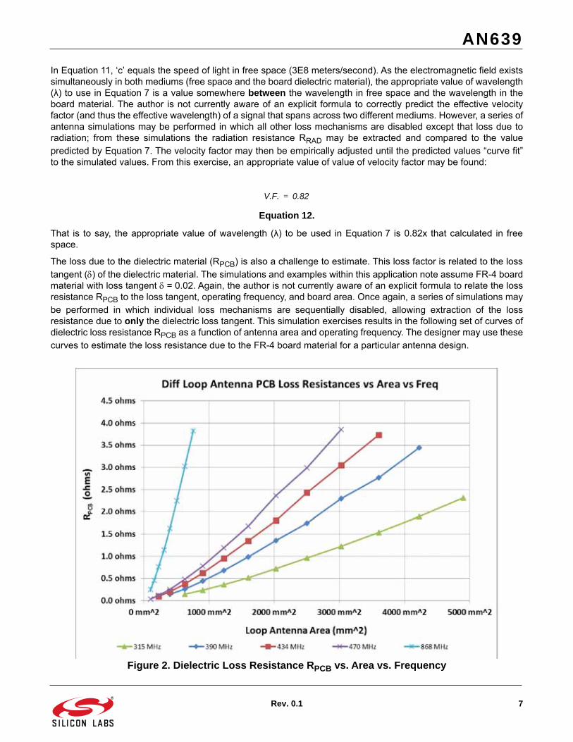
In Equation 11, ‘c’ equals the speed of light in free space (3E8 meters/second). As the electromagnetic field existssimultaneously in both mediums (free space and the board dielectric material), the appropriate value of wavelength(λ) to use in Equation 7 is a value somewhere between the wavelength in free space and the wavelength in theboard material. The author is not currently aware of an explicit formula to correctly predict the effective velocityfactor (and thus the effective wavelength) of a signal that spans across two different mediums. However, a series ofantenna simulations may be performed in which all other loss mechanisms are disabled except that loss due toradiation; from these simulations the radiation resistance RRAD may be extracted and compared to the valuepredicted by Equation 7. The velocity factor may then be empirically adjusted until the predicted values “curve fit”to the simulated values. From this exercise, an appropriate value of value of velocity factor may be found:
Equation 12.
That is to say, the appropriate value of wavelength (λ) to be used in Equation 7 is 0.82x that calculated in freespace.
The loss due to the dielectric material (RPCB) is also a challenge to estimate. This loss factor is related to the losstangent () of the dielectric material. The simulations and examples within this application note assume FR-4 boardmaterial with loss tangent = 0.02. Again, the author is not currently aware of an explicit formula to relate the lossresistance RPCB to the loss tangent, operating frequency, and board area. Once again, a series of simulations maybe performed in which individual loss mechanisms are sequentially disabled, allowing extraction of the lossresistance due to only the dielectric loss tangent. This simulation exercises results in the following set of curves ofdielectric loss resistance RPCB as a function of antenna area and operating frequency. The designer may use thesecurves to estimate the loss resistance due to the FR-4 board material for a particular antenna design.
Figure 2. Dielectric Loss Resistance RPCB vs. Area vs. Frequency
V.F. 0.82=

AN639
8 Rev. 0.1
4. Loop Antenna Practical DesignArmed with knowledge of these basic design equations and performance curves, it is now possible to design apractical loop antenna. As an example, the area of a loop antenna that fully occupies the available space within a
typical remote keyless entry (RKE) keyfob for an automobile may be only 40 mm x 25 mm = 1000 mm2. A tracewidth of 1.0 mm is assumed with a copper weight of 1 oz.
F = 434 MHz
a1 = 40 mm
a2 = 25 mm
t = 0.035 mm (1 oz. copper)
w = 1.0 mm
Application of Equation 7 at an operating frequency of F = 434 MHz and applying the empirically-derived velocityfactor of V.F. = 0.82 results in:
Equation 13.
Application of Equation 10 results in a calculated value of trace resistance RTRACE of:
Equation 14.
It is evident that the loss due to the trace resistance exceeds the radiation resistance, and thus the radiationefficiency is expected to be relatively low (refer to Equation 9). The radiation efficiency will degrade even further asthe remaining loss mechanisms (i.e., dielectric loss and component ESR) are accounted for.
The dielectric loss resistance may be estimated from the curves of Equation 2 as being RPCB = ~0.7 Ω at an
operating frequency of 434 MHz and loop area of 1000 mm2.
The inductance of the loop antenna may be calculated from Equation 4 and Equation 5 as:
Equation 15.
An equivalent lumped-element model of the loop antenna is simply an inductor in series with a resistor. Theinductance may be resonated with a capacitor of value:
Equation 16.
RRAD 3204 0.04 0.025 2
0.82 3E8/434E6 4------------------------------------------------------- 0.302 = =
RTRACE2 0.04 2 0.025+
2 0.001---------------------------------------------------- 434E6 1.256E 6–
5.8E7------------------------------------------------------------- 0.353 = =
L2 o a1 a2
---------------------------------------------
a1 a2b
---------------------- ln 0.774– 102.64 nH= =
C 12f 2L
-------------------- 1.31pF= =

AN639
Rev. 0.1 9
The equivalent series resistance (RESR) of this capacitor is a function of its Q-factor. A reasonable estimate of theQ of surface-mount ceramic capacitors (e.g., Murata GJM1555 series) is Q ≈ 350. The RESR may be calculated as:
Equation 17.
The total series resistance may be calculated as:
Equation 18.
The expected antenna efficiency may be estimated by Equation 9 as:
Equation 19.
The antenna efficiency may be expressed in dBi (dB relative to an isotropic antenna):
Equation 20.
This quantity represents the radiation efficiency of the antenna when summed over all spatial directions. Theantenna gain typically measured in a lab environment or antenna chamber reflects the product of the antennaefficiency and the antenna directivity.
The loop antenna may be brought to parallel resonance by placing this capacitor across the input terminals of thedifferential loop antenna.
RESR
XC
Q------- 1
2fCQ------------------ 1
2 434E6 1.31pF 350------------------------------------------------------------------------ 0.799 = = = =
RSER RRAD RTRACE RPCB RESR+ + + 0.302 0.353 0.7 0.799+ + + 2.154 = = =
r
RRAD
RRAD RTRACE RPCB RESR+ + +------------------------------------------------------------------------------------- 0.302
2.154--------------- 0.14= = =
GANT_EFF 10 r log 8.53 dBi–= =

AN639
10 Rev. 0.1
Figure 3. Series and Parallel Lumped Equivalent Models
The series equivalent lumped element model may be transformed into a parallel equivalent model, as shown inFigure 3. Due to the high Q-factor of the network, the parallel values of L and C remain (approximately) the same,while the parallel resistance may be calculated as:
Equation 21.
Equation 22.
The total series resistance of a loop antenna was observed to be quite low (a few ohms or less); in contrast, thetransformed parallel resistance is quite high (several tens of kilohms). Without further impedance matching, thishigh value of resistance would be observed at the input terminals of the antenna at parallel resonance (i.e., at thefrequency where the reactances of LP and CP cancel each other).
As this antenna impedance is much higher than the typical output impedance of a PA circuit or input impedance ofan LNA circuit, it is common to transform this high impedance downwards to better match the impedance of thecircuit. This impedance transformation may be provided by discrete capacitors, discrete inductors, distributedtransmission lines, or a combination thereof; however, the most commonly used method is “capacitive-tapping,” asshown in Figure 4. Capacitors are typically used as discrete matching elements because their Q-factor is usuallymuch higher than inductors, causing them to minimize any additional loss in the match.
XLSER 2fL 2 434E6 102.64nH 279.89 = = =
RP RSER 1 QSER 2+ RSER 1XLSER
RSER----------------- 2
+ 2.154 1 279.89
2.154------------------ +
2
36.37 k = = = =

AN639
Rev. 0.1 11
Figure 4. Capacitive-Tapping Impedance Transformation
The exact equations for expressing the input impedance ZIN as a function of LP, RP, CP1, and CP2 are rathertedious. However, the high-Q nature of the antenna circuit allows use of some approximations that significantlysimplify the equations, resulting in the following expressions:
Equation 23.
Equation 24.
Here, RIN is the desired impedance to which to match the antenna.
From Equation 24, it is evident that a large impedance transformation ratio (i.e., a low value of RIN) is obtained byusing a small ratio of CP1:CP2, that is, the value of CP1 must be much less than CP2. From this, the following twoobservations may be made:
The resonant frequency of the antenna is controlled (primarily) by adjusting CP1.
The transformed impedance seen at the antenna input is controlled by adjusting the ratio of CP2:CP1.
The PA output circuit of the Si4010 chip is a switched programmable current source that delivers pulses of currentto the load impedance. Thus, the amount of power delivered to the load (i.e., antenna) is given by the well-knownequation:
Equation 25.
Cp
Cp1Cp2Cp1 Cp2+--------------------------=
Rp
RIN--------- 1
Cp2Cp1----------+
2=
POUT IPA_BIAS R2
IN=
AN639
12 Rev. 0.1
It is clear that the power delivered to the load may be increased by raising either the PA bias current or the antennaload resistance. However, this relationship only holds true up to the point where the output voltage swing(V = IPA_BIAS x RIN) exceeds the value at which voltage clipping occurs in the PA output devices. For the Si4010chip configured for the maximum value of PA bias current, the load resistance at which clipping occurs isRIN ≈ 500 Ω. As a result, this value is often stated as being the optimal load resistance for the Si4010 chip, and isusually the design target for the input impedance of a loop antenna.
The required ratio of CP2:CP1 may then be calculated from Equation 24.
Equation 26.
Equation 27.
Equation 23 and Equation 27 may now be solved simultaneously for the individual values of CP1 and CP2 (recallingthat CP is the total value of capacitance required to resonate the antenna inductance).
CP1 = 1.484 pF
CP2 = 11.17 pF
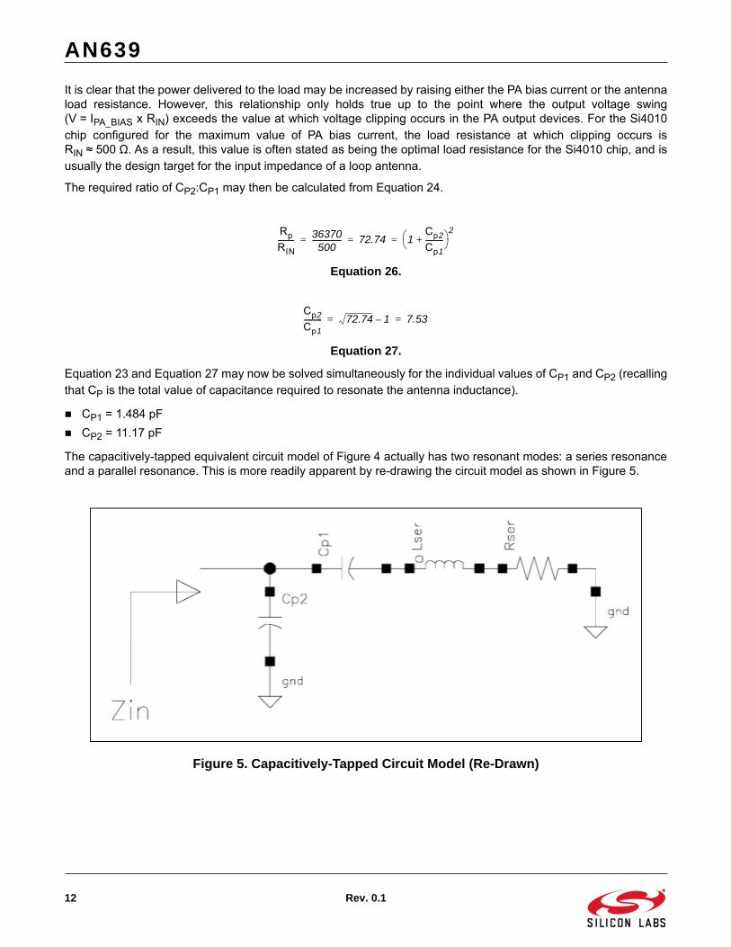
The capacitively-tapped equivalent circuit model of Figure 4 actually has two resonant modes: a series resonanceand a parallel resonance. This is more readily apparent by re-drawing the circuit model as shown in Figure 5.
Figure 5. Capacitively-Tapped Circuit Model (Re-Drawn)
Rp
RIN--------- 36370
500---------------- 72.74 1
Cp2Cp1----------+
2= = =
Cp2Cp1---------- 72.74 1– 7.53= =

AN639
Rev. 0.1 13
It is evident that LSER will achieve series-resonance with CP1 at some frequency FSER. Above this series resonantfrequency, the LSER-RSER-CP1 arm will appear inductive and will subsequently achieve parallel-resonance withCP2 at some frequency FPAR. This parallel-resonant frequency FPAR is the desired operating frequency for the loopantenna and is always located above FSER, for this type of matching network.
The lumped element equivalent circuit model of Figure 5 may be simulated for its impedance behavior overfrequency, using the component values calculated previously and summarized below:
L = 120.64 nH
CP1 = 1.484 pF
CP2 = 11.17 pF
RSER = 2.154 Ω
The simulated Mag(Zin) response of the equivalent circuit model is shown in Figure 6. The series and parallelresonant frequencies are clearly apparent.
Figure 6. Mag(Zin) Response of Capacitively-Tapped Circuit Model
AN639
14 Rev. 0.1
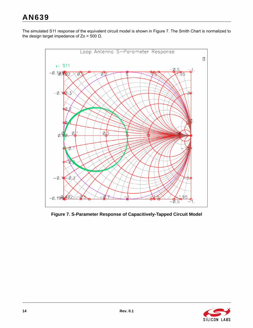
The simulated S11 response of the equivalent circuit model is shown in Figure 7. The Smith Chart is normalized tothe design target impedance of Zo = 500 Ω.
Figure 7. S-Parameter Response of Capacitively-Tapped Circuit Model
AN639
Rev. 0.1 15
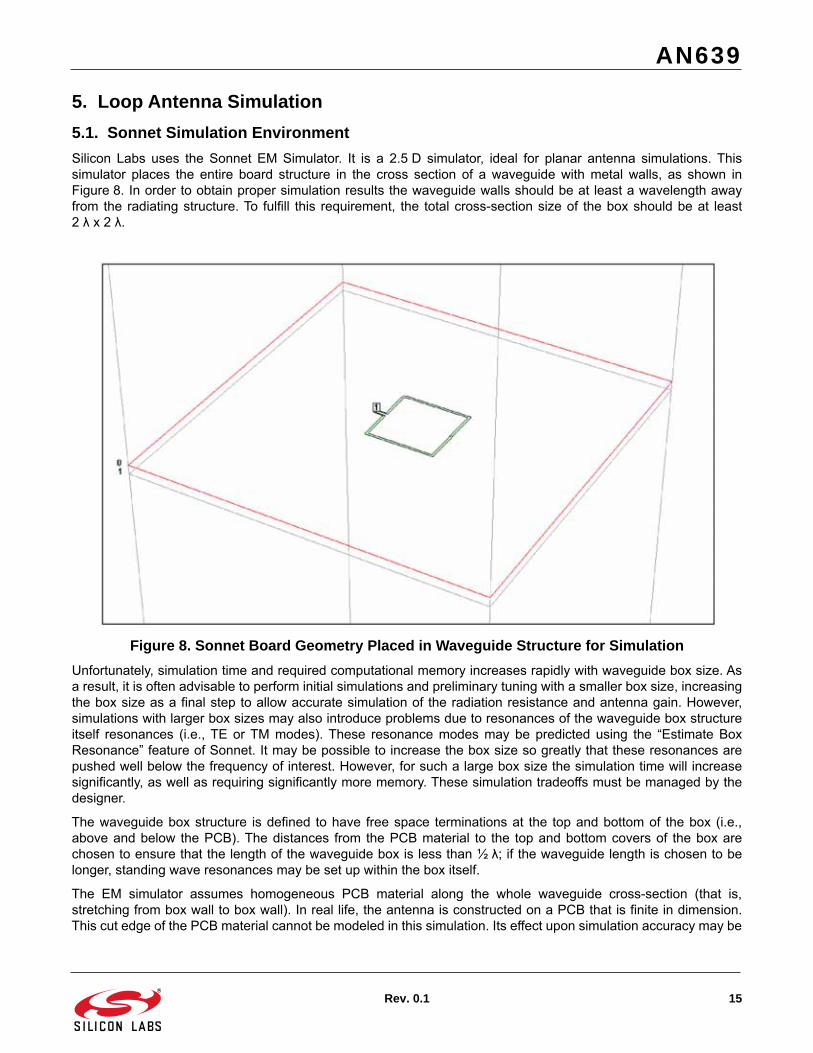
5. Loop Antenna Simulation5.1. Sonnet Simulation EnvironmentSilicon Labs uses the Sonnet EM Simulator. It is a 2.5 D simulator, ideal for planar antenna simulations. Thissimulator places the entire board structure in the cross section of a waveguide with metal walls, as shown inFigure 8. In order to obtain proper simulation results the waveguide walls should be at least a wavelength awayfrom the radiating structure. To fulfill this requirement, the total cross-section size of the box should be at least2 λ x 2 λ.
Figure 8. Sonnet Board Geometry Placed in Waveguide Structure for SimulationUnfortunately, simulation time and required computational memory increases rapidly with waveguide box size. Asa result, it is often advisable to perform initial simulations and preliminary tuning with a smaller box size, increasingthe box size as a final step to allow accurate simulation of the radiation resistance and antenna gain. However,simulations with larger box sizes may also introduce problems due to resonances of the waveguide box structureitself resonances (i.e., TE or TM modes). These resonance modes may be predicted using the “Estimate BoxResonance” feature of Sonnet. It may be possible to increase the box size so greatly that these resonances arepushed well below the frequency of interest. However, for such a large box size the simulation time will increasesignificantly, as well as requiring significantly more memory. These simulation tradeoffs must be managed by thedesigner.
The waveguide box structure is defined to have free space terminations at the top and bottom of the box (i.e.,above and below the PCB). The distances from the PCB material to the top and bottom covers of the box arechosen to ensure that the length of the waveguide box is less than ½ λ; if the waveguide length is chosen to belonger, standing wave resonances may be set up within the box itself.
The EM simulator assumes homogeneous PCB material along the whole waveguide cross-section (that is,stretching from box wall to box wall). In real life, the antenna is constructed on a PCB that is finite in dimension.This cut edge of the PCB material cannot be modeled in this simulation. Its effect upon simulation accuracy may be

AN639
16 Rev. 0.1
minimized by ensuring that there is at least ~2 mm distance between the trace(s) of the loop antenna and the cutedge of the PCB material. This should be achievable in most antenna designs.
Additionally, certain features such as mounting holes or board slots cannot be simulated in Sonnet. The Sonnetsimulator assumes the dielectric PCB material to be homogeneous and unbroken, stretching from box wall to boxwall. There is no capability within Sonnet to “punch holes” within this dielectric material, and thus it is not possibleto model the effect (if any) of mounting holes upon the performance of the antenna. However, from experience thisinfluence is expected to be very slight.
It is theoretically possible to construct a simulation model that accounts for the presence of a large mass of metalnear the loop antenna structure, such as a coin-cell battery. This is accomplished through the use of a “ThickMetal” structure in Sonnet. However, the memory requirements and simulation time increase drastically when thickmetal structures are used.
The loop antenna structures discussed within this document are all differential structures. Therefore, the Sonnetsimulation must be constructed to simulate the differential impedance of the loop antenna. In Sonnet, this isaccomplished by placing the simulation port (Port 1) between the differential traces feeding the antenna structure.Reliable S parameter results may be obtained when using internal ports as long as the ports are ungrounded anddifferential. In such a case, it is not necessary to use ports situated at the box wall. As a result, the problematiceffects of de-embedding long differential transmission lines are avoided.
It is normal for areas of the board that are not used for the loop antenna structure to be poured with GND plane. Inthe simulations shown within this document, these GND planes are removed in order to simplify the antennamodel. As the simulated impedance is taken differentially between the feed lines of the antenna, there is no needfor a local GND reference for the measurement port. Furthermore, this simulation model matches real-life antennaapplications; in a typical hand-held design (e.g., keyfob) there is no connection between the local GND plane (i.e.,negative terminal of the coin-cell battery) and earth GND.
5.2. Loop Antenna Impedance Simulation ExampleThe substrate material chosen for a design example is 0.8 mm thick FR-4, with an assumed dielectric relativepermittivity of εr = 4.6 and a loss tangent (dissipation factor) of = 0.02. The board dimensions and loop antennasize typically vary as a function of the desired frequency of operation; however, this section continues with theprevious design example at 434 MHz with loop dimensions of 40 mm x 25 mm, as shown in Figure 9. The width ofthe loop antenna traces are 1.0 mm, and 1-oz copper ( = 5.8E7 Siemens/meter) is assumed.
Inspection of the geometry of Figure 9 shows dimensions of 39 mm x 24 mm, instead of the mentioned values of40 mm x 25 mm. However, these dimensions are referenced from the inside edges of the antenna traces, while theequations developed in Section 3 and Figure 1 used dimensions referenced to the center of the traces. The loopdimensions are therefore equivalent.
The tuning capacitors CP1 and CP2 are implemented as ideal capacitors, but in parallel with an ideal resistor whosevalue is calculated to represent the equivalent parallel resistance due to the finite Q-factor of the capacitors. The Qof the capacitors is assumed to be Q = 350, a reasonable value for surface-mount ceramic capacitors. The seriestuning capacitor CP1 is physically placed at the top-center of the loop, while the parallel tuning capacitor CP2 isplaced across the input feed lines of the loop antenna. The Si4010 chip internally integrates an adjustable bank ofcapacitors across its TXP and TXM output pins (i.e., connecting to the feed lines of the loop antenna), and thus(depending on required value) there may be no need for an additional explicit CP2 capacitor, external to the chip.

AN639
Rev. 0.1 17
Figure 9. Sonnet Simulation Geometry for Example Loop AntennaThe initial simulated Mag(Zin) impedance behavior of this loop antenna is shown in Figure 10. It is apparent thatwhile the input impedance is close to our design target (Zin ≈ 640 Ω, compared with target Zin = 500 Ω), theresonant frequency of this initial design is at ~397 MHz, well below our design target of 434 MHz. In other words,the agreement between simulation results and the theoretical design equations is not exact.
One reason for this discrepancy is the physical size of the loop antenna. A fundamental assumption underlying thedevelopment of the design equations in Section 3 is that the size of the loop is small compared to the wavelengthat the desired operating frequency. If this assumption holds true, the instantaneous current is identical at alllocations in the antenna, thus greatly simplifying the development of the theoretical equations. However, as theloop dimensions increase, the antenna traces begin to behave more like transmission lines instead of simpleinductors. In such a case, the amplitude and phase of the instantaneous current may vary from one location toanother along the antenna traces.
It is actually possible to construct a loop antenna of sufficient size so that it achieves parallel self-resonance on itsown, without the need for a resonating capacitance. Antenna traces of such length therefore appear as a largereffective inductance than suggested by Equation 4, resulting in a lower actual frequency of resonance thanpredicted by the design equations.
The antenna designer is thus often presented with the following contradictory design goals:
Maximize the loop antenna dimensions to optimize radiation resistance (which optimizes antenna efficiency).
Use of a loop antenna with moderate dimensions to obtain good agreement with theoretical design equations.
The antenna designer must accept that theoretical design equations may be used to obtain a preliminary designthat is close to the desired performance, but a subsequent round of simulation and/or bench tuning is also usuallynecessary to perfect the design.
AN639
18 Rev. 0.1
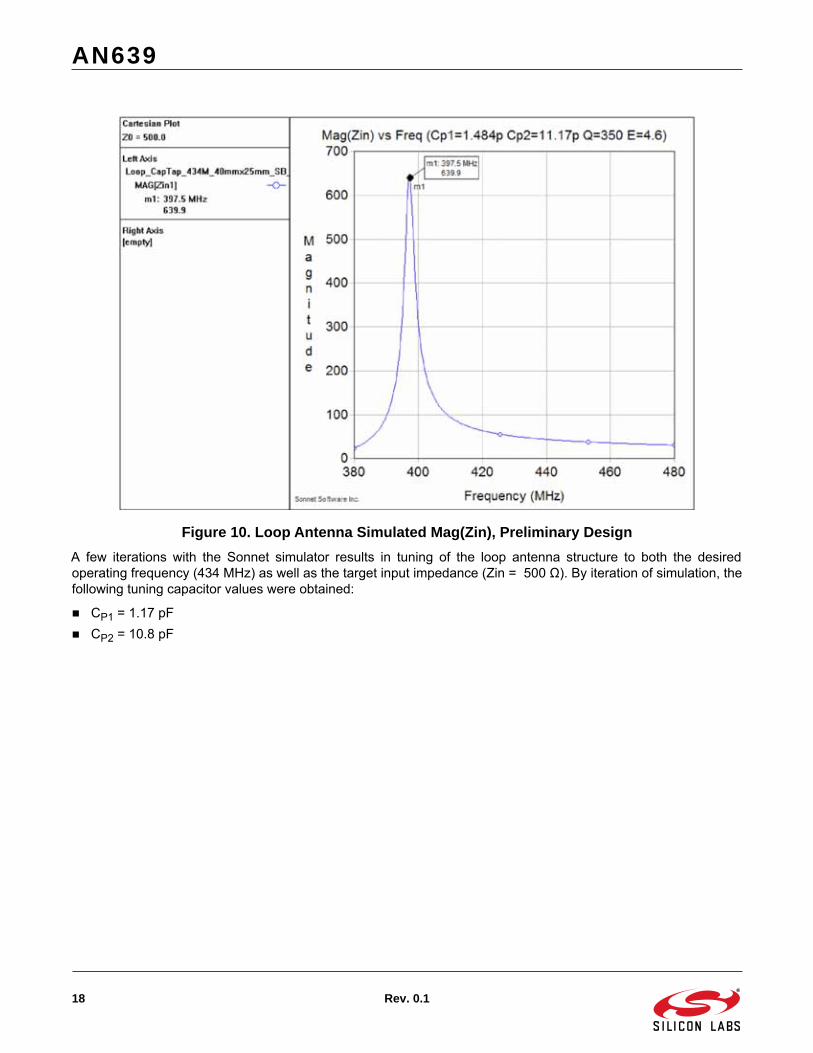
Figure 10. Loop Antenna Simulated Mag(Zin), Preliminary DesignA few iterations with the Sonnet simulator results in tuning of the loop antenna structure to both the desiredoperating frequency (434 MHz) as well as the target input impedance (Zin = 500 Ω). By iteration of simulation, thefollowing tuning capacitor values were obtained:
CP1 = 1.17 pF
CP2 = 10.8 pF

AN639
Rev. 0.1 19
The simulated Mag(Zin) impedance response of the final design is shown in Figure 11. The series-resonant andparallel-resonant frequencies are clearly evident, as discussed in Figure 6.
Figure 11. . Loop Antenna Simulated Mag(Zin), Final DesignThe results of this design example indicate that a typical keyfob differential loop antenna may operate with a veryhigh L:C ratio; that is, a small value of capacitance resonates a large value of inductance. In the higher frequencybands (868 to 915 MHz), the required value of total capacitance (CP) may be very small (less than 0.5 pF). Withsuch small values of capacitance, the tuning of the antenna may become sensitive to component tolerancevariations. To some extent, this effect may be reduced by adjusting the size of the antenna (i.e., value of antennatrace inductance). With a smaller loop antenna, higher values of capacitance are required to tune the antenna toresonance, thus reducing the sensitivity of the design to component tolerances. However, the radiation resistance(and thus antenna efficiency) drops as the size of the loop antenna is decreased, as shown by Equation 7. Thusfrequency tuning range may need to be traded off against antenna efficiency and link range.
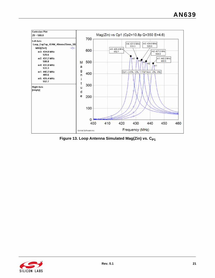
Inspection of Equation 23 and Equation 24 show that tuning the resonant frequency of the antenna is dominated byCP1, while the transformed input impedance of the antenna is determined by the ratio of CP2:CP1. Insight into thetuning of both the resonant frequency and input impedance may be gained by sweeping the CP1 and CP2
capacitance values as parametric variables. In the plot of Figure 12, the tuning capacitance CP2 is varied; in theplot of Figure 13, the tuning capacitor CP1 is varied. From inspection of these two tuning curves, it is evident thatthe tuning of the loop antenna is affected in the following manner:
An increase (decrease) in value of either capacitor value lowers (raises) the resonant frequency.
Increasing (decreasing) the value of CP1 moderately raises (lowers) the input impedance.
Increasing (decreasing) the value of CP2 significantly lowers (raises) the input impedance.
As the input terminals of the differential loop antenna are connected to the RFIC (i.e., TX output or LNA input), thelogical component to be automatically adjusted by any tuning circuitry integrated within the chip (e.g. Si4010) is theCP2 capacitor. While adjustment of this capacitor is effective in tuning the resonant frequency of the loop, it has the

AN639
20 Rev. 0.1
unfortunate side effect of also providing the greatest variation in input impedance. A more effective way of tuningthe loop would be to vary the CP1 component value. However, this tuning approach turns out to be quite difficult.The voltage appearing across CP1 is quite large due to the effects of impedance transformation, and would provedifficult to control with conventional integrated devices (i.e., CMOS). Automated tuning of the CP1 tuning capacitoris currently not provided by the Si4010 chip.
Figure 12. Loop Antenna Simulated Mag(Zin) vs. CP2
AN639
Rev. 0.1 21
Figure 13. Loop Antenna Simulated Mag(Zin) vs. CP1

AN639
22 Rev. 0.1
5.3. Loop Antenna Gain Simulation ExampleThe radiation patterns and field strengths of the antenna design may also be simulated. This is useful fordetermining the radiation efficiency of each design. Memory limitations of the Sonnet simulator generally requiresimplification of the antenna model and limiting the waveguide box size to approximately 2λ x 2λ. This is usuallylarge enough to get a reasonable estimate of the true far-field radiated performance. It is also sufficient fordetermining the relative performance of various antenna structures.
The spherical coordinate system used by Sonnet in their far-field viewer is shown in Figure 14. The board isassumed to lie in the X-Y plane, with the Z-dimension in the vertical direction (orthogonal to the plane of the PCB).The variable ‘θ’ measures the angle relative to this vertical axis, and thus a value of θ = 0 deg represents a vectorperpendicular to the plane of the board, while a value of θ = +90 deg or θ = –90 deg lies in the plane of the boarditself. The variable ‘’ measures the angle relative to the horizontal bottom edge of the board geometry, as drawn inthe previous antenna design examples. Thus a value of = 0 deg represents a vector towards the right-hand edgeof the geometry window (i.e., top of the loop antenna in the designs shown here), while a value of = +90 degrepresents a vector towards the upper edge of the geometry window. In such a coordinate system, the variable ‘’corresponds to azimuth while the variable ‘θ’ corresponds to elevation.
One known limitation of the Sonnet simulator is that radiation patterns falling in the exact plane of the antennastructure itself (i.e., plane of the PCB) are not simulated accurately. The simulator tends to produce radiationpatterns with nulls (zero radiated field strength) or discontinuously large values. The results for these values of θ(θ=±90 deg) should be ignored.
Figure 14. Spherical Coordinate System Used by Sonnet Far-Field Viewer
AN639
Rev. 0.1 23
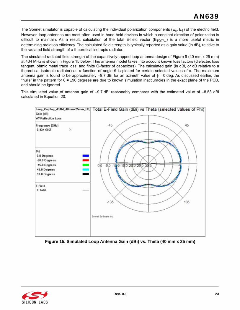
The Sonnet simulator is capable of calculating the individual polarization components (E, Eθ) of the electric field.However, loop antennas are most often used in hand-held devices in which a constant direction of polarization isdifficult to maintain. As a result, calculation of the total E-field vector (ETOTAL) is a more useful metric indetermining radiation efficiency. The calculated field strength is typically reported as a gain value (in dB), relative tothe radiated field strength of a theoretical isotropic radiator.
The simulated radiated field strength of the capacitively-tapped loop antenna design of Figure 9 (40 mm x 25 mm)at 434 MHz is shown in Figure 15 below. This antenna model takes into account known loss factors (dielectric losstangent, ohmic metal trace loss, and finite Q-factor of capacitors). The calculated gain (in dBi, or dB relative to atheoretical isotropic radiator) as a function of angle θ is plotted for certain selected values of . The maximumantenna gain is found to be approximately –9.7 dBi for an azimuth value of = 0 deg. As discussed earlier, the“nulls” in the pattern for θ = ±90 degrees are due to known simulation inaccuracies in the exact plane of the PCB,and should be ignored.
This simulated value of antenna gain of –9.7 dBi reasonably compares with the estimated value of –8.53 dBicalculated in Equation 20.
Figure 15. Simulated Loop Antenna Gain (dBi) vs. Theta (40 mm x 25 mm)

AN639
24 Rev. 0.1
This plot should be interpreted as viewing the PCB “edge on” in the horizontal plane. Thus the E-field gain valuesfor –90 deg < θ < +90 deg represent the portion of the radiation pattern lying above the plane of the board; the E-field gain values for +90 deg < θ < +180 deg and –180 deg < θ < –90 deg represent the portion of the radiationpattern lying below the plane of the board. Each selected value of represents a different angle or viewpoint fromwhich to view the horizontal edge of the board (i.e., azimuth). Thus the radiation pattern of Figure 15 depicts anantenna that radiates optimally at an angle just slightly above the plane of the PCB, with a moderate dip in radiationintensity in a direction vertically perpendicular to the board.
It is also useful to plot the radiated field strength as a function of azimuth angle , for certain selected values of θ.This is illustrated in Figure 16. The maximum antenna gain is again found to be approximately –9.7 dBi for anelevation angle of θ = ±85 deg (i.e., just above the plane of the PCB).
Figure 16. Simulated Loop Antenna Gain (dBi) vs. Phi (40 mm x 25 mm)This plot should be interpreted as viewing the antenna pattern from a point in space located directly above thePCB, looking downwards towards the antenna structure. The E-field gain values as a function of thus representthe variation in radiated field strength around the perimeter of the board (i.e., for a change in azimuth). Eachselected value of θ represents a different angle of elevation (relative to the vertical axis). Thus, the radiation patternof Figure 16 depicts an antenna that radiates nearly equally in all directions of azimuth (i.e., is omni-directional),but varies somewhat with respect to elevation angle above or below the board.
AN639
Rev. 0.1 25
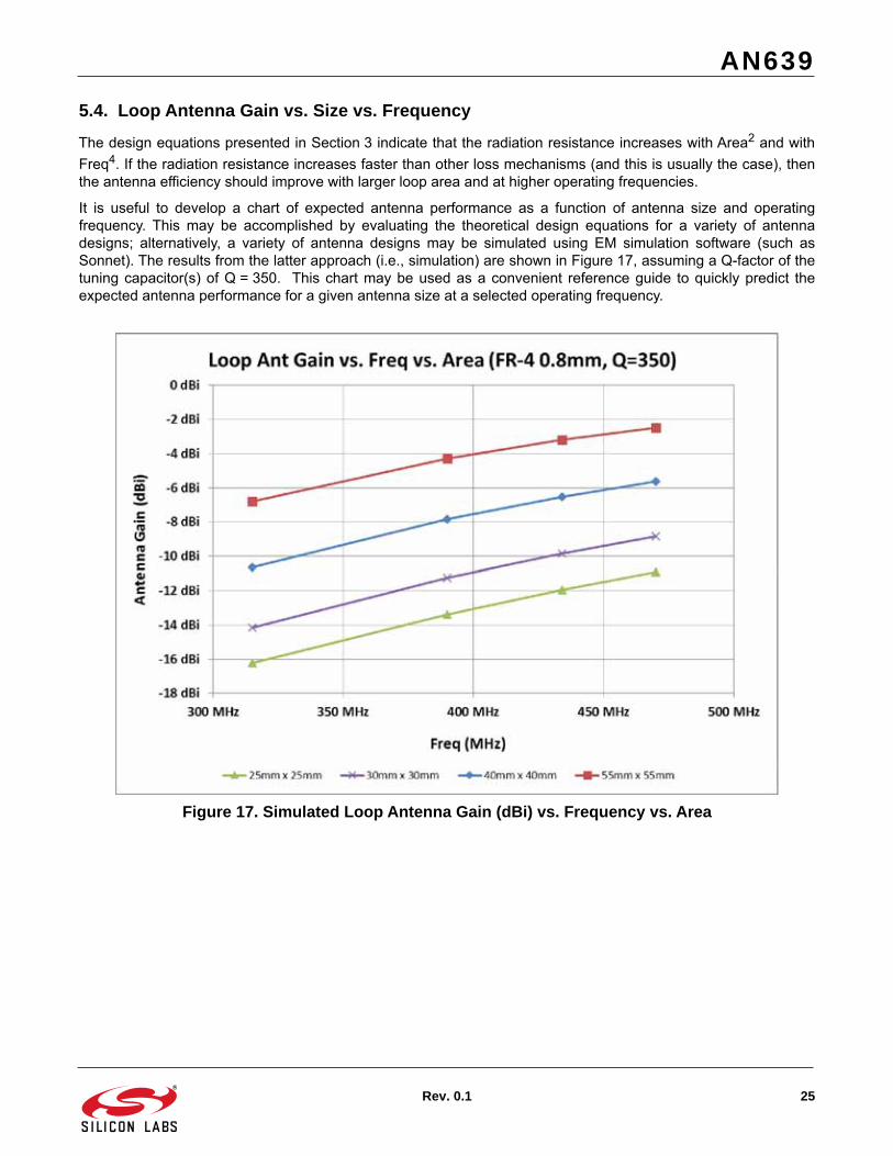
5.4. Loop Antenna Gain vs. Size vs. Frequency
The design equations presented in Section 3 indicate that the radiation resistance increases with Area2 and with
Freq4. If the radiation resistance increases faster than other loss mechanisms (and this is usually the case), thenthe antenna efficiency should improve with larger loop area and at higher operating frequencies.
It is useful to develop a chart of expected antenna performance as a function of antenna size and operatingfrequency. This may be accomplished by evaluating the theoretical design equations for a variety of antennadesigns; alternatively, a variety of antenna designs may be simulated using EM simulation software (such asSonnet). The results from the latter approach (i.e., simulation) are shown in Figure 17, assuming a Q-factor of thetuning capacitor(s) of Q = 350. This chart may be used as a convenient reference guide to quickly predict theexpected antenna performance for a given antenna size at a selected operating frequency.
Figure 17. Simulated Loop Antenna Gain (dBi) vs. Frequency vs. Area
AN639
26 Rev. 0.1
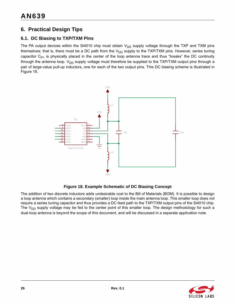
6. Practical Design Tips6.1. DC Biasing to TXP/TXM PinsThe PA output devices within the Si4010 chip must obtain VDD supply voltage through the TXP and TXM pinsthemselves; that is, there must be a DC path from the VDD supply to the TXP/TXM pins. However, series tuningcapacitor CP1 is physically placed in the center of the loop antenna trace and thus “breaks” the DC continuitythrough the antenna loop. VDD supply voltage must therefore be supplied to the TXP/TXM output pins through apair of large-value pull-up inductors, one for each of the two output pins. This DC biasing scheme is illustrated inFigure 18.
Figure 18. Example Schematic of DC Biasing ConceptThe addition of two discrete inductors adds undesirable cost to the Bill of Materials (BOM). It is possible to designa loop antenna which contains a secondary (smaller) loop inside the main antenna loop. This smaller loop does notrequire a series tuning capacitor and thus provides a DC feed path to the TXP/TXM output pins of the Si4010 chip.The VDD supply voltage may be fed to the center point of this smaller loop. The design methodology for such adual-loop antenna is beyond the scope of this document, and will be discussed in a separate application note.
AN639
Rev. 0.1 27
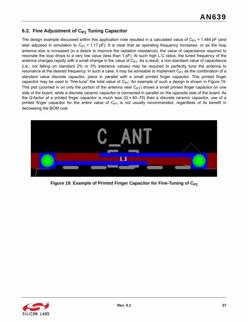
6.2. Fine Adjustment of CP1 Tuning CapacitorThe design example discussed within this application note resulted in a calculated value of CP1 = 1.484 pF (andlater adjusted in simulation to CP1 = 1.17 pF). It is clear that as operating frequency increases, or as the loopantenna size is increased (in a desire to improve the radiation resistance), the value of capacitance required toresonate the loop drops to a very low value (less than 1 pF). At such high L:C ratios, the tuned frequency of theantenna changes rapidly with a small change in the value of CP1. As a result, a non-standard value of capacitance(i.e., not falling on standard 2% or 5% tolerance values) may be required to perfectly tune the antenna toresonance at the desired frequency. In such a case, it may be advisable to implement CP1 as the combination of astandard value discrete capacitor, place in parallel with a small printed finger capacitor. This printed fingercapacitor may be used to “fine-tune” the total value of CP1. An example of such a design is shown in Figure 19.This plot (zoomed in on only the portion of the antenna near CP1) shows a small printed finger capacitor on oneside of the board, while a discrete ceramic capacitor is connected in parallel on the opposite side of the board. Asthe Q-factor of a printed finger capacitor is much less (Q ≈ 60–70) than a discrete ceramic capacitor, use of aprinted finger capacitor for the entire value of CP1 is not usually recommended, regardless of its benefit indecreasing the BOM cost.
Figure 19. Example of Printed Finger Capacitor for Fine-Tuning of CP1

http://www.silabs.com
Silicon Laboratories Inc.400 West Cesar ChavezAustin, TX 78701USA
Smart. Connected. Energy-Friendly.
Productswww.silabs.com/products
Qualitywww.silabs.com/quality
Support and Communitycommunity.silabs.com
DisclaimerSilicon Labs intends to provide customers with the latest, accurate, and in-depth documentation of all peripherals and modules available for system and software implementers using or intending to use the Silicon Labs products. Characterization data, available modules and peripherals, memory sizes and memory addresses refer to each specific device, and "Typical" parameters provided can and do vary in different applications. Application examples described herein are for illustrative purposes only. Silicon Labs reserves the right to make changes without further notice and limitation to product information, specifications, and descriptions herein, and does not give warranties as to the accuracy or completeness of the included information. Silicon Labs shall have no liability for the consequences of use of the information supplied herein. This document does not imply or express copyright licenses granted hereunder to design or fabricate any integrated circuits. The products are not designed or authorized to be used within any Life Support System without the specific written consent of Silicon Labs. A "Life Support System" is any product or system intended to support or sustain life and/or health, which, if it fails, can be reasonably expected to result in significant personal injury or death. Silicon Labs products are not designed or authorized for military applications. Silicon Labs products shall under no circumstances be used in weapons of mass destruction including (but not limited to) nuclear, biological or chemical weapons, or missiles capable of delivering such weapons.
Trademark InformationSilicon Laboratories Inc.® , Silicon Laboratories®, Silicon Labs®, SiLabs® and the Silicon Labs logo®, Bluegiga®, Bluegiga Logo®, Clockbuilder®, CMEMS®, DSPLL®, EFM®, EFM32®, EFR, Ember®, Energy Micro, Energy Micro logo and combinations thereof, "the world’s most energy friendly microcontrollers", Ember®, EZLink®, EZRadio®, EZRadioPRO®, Gecko®, ISOmodem®, Precision32®, ProSLIC®, Simplicity Studio®, SiPHY®, Telegesis, the Telegesis Logo®, USBXpress® and others are trademarks or registered trademarks of Silicon Labs. ARM, CORTEX, Cortex-M3 and THUMB are trademarks or registered trademarks of ARM Holdings. Keil is a registered trademark of ARM Limited. All other products or brand names mentioned herein are trademarks of their respective holders.