DESIGN OF PLANAR DUAL AND TRIPLE NARROW- BAND … of planar dual and triple narrow-band...DESIGN OF...
16
Progress In Electromagnetics Research, Vol. 131, 259–274, 2012 DESIGN OF PLANAR DUAL AND TRIPLE NARROW- BAND BANDSTOP FILTERS WITH INDEPENDENTLY CONTROLLED STOPBANDS AND IMPROVED SPURI- OUS RESPONSE H. Ning 1, * , J. Wang 1 , Q. Xiong 1 , and L. Mao 2 1 School of Electronic and Information Engineering, Beihang University, Beijing 100191, China 2 Institute of Intelligent Structure and System, Soochow University, Suzhou, Jiangsu 215006, China Abstract—A novel design of planar dual and triple narrow-band bandstop filter is presented by adopting the proposed meandered slot defected microstrip structure (MS-DMS) and the simplified spiral microstrip resonator (SSMR). Through this design, the stopbands of the dual- and triple-band bandstop filters can be individually controlled and the improved spurious responses are achieved. First, the fundamental and the first spurious resonances of the MS-DMS and SSMR are analyzed to provide the design rules. Then, by utilizing the prominent stopband of the MS-DMS and the stopband produced by the SSMR coupled to main microstrip line, a dual narrow- band bandstop filter is constructed before its design procedure is outlined. Based on above investigations, a triple narrow-band bandstop filter is implemented by inserting extra SSMRs to another side of the main microstrip line of the dual-band filter to generate a new stopband. To verify the aforementioned design concepts, a dual and triple narrow-band bandstop filter are designed, simulated and tested. Both the simulation and measurement indicate that the fabricated filters exhibit good stopband/passband performance and improved first spurious resonance. Moreover, these filters are simple to design and quite compatible with planar fabrication technique, making them very attractive for practical applications. Received 21 July 2012, Accepted 5 September 2012, Scheduled 12 September 2012 * Corresponding author: Huansheng Ning ([email protected]).
Transcript of DESIGN OF PLANAR DUAL AND TRIPLE NARROW- BAND … of planar dual and triple narrow-band...DESIGN OF...

Progress In Electromagnetics Research, Vol. 131, 259–274, 2012
DESIGN OF PLANAR DUAL AND TRIPLE NARROW-BAND BANDSTOP FILTERS WITH INDEPENDENTLYCONTROLLED STOPBANDS AND IMPROVED SPURI-OUS RESPONSE
H. Ning1, *, J. Wang1, Q. Xiong1, and L. Mao2
1School of Electronic and Information Engineering, Beihang University,Beijing 100191, China2Institute of Intelligent Structure and System, Soochow University,Suzhou, Jiangsu 215006, China
Abstract—A novel design of planar dual and triple narrow-bandbandstop filter is presented by adopting the proposed meanderedslot defected microstrip structure (MS-DMS) and the simplified spiralmicrostrip resonator (SSMR). Through this design, the stopbandsof the dual- and triple-band bandstop filters can be individuallycontrolled and the improved spurious responses are achieved. First,the fundamental and the first spurious resonances of the MS-DMSand SSMR are analyzed to provide the design rules. Then, byutilizing the prominent stopband of the MS-DMS and the stopbandproduced by the SSMR coupled to main microstrip line, a dual narrow-band bandstop filter is constructed before its design procedure isoutlined. Based on above investigations, a triple narrow-band bandstopfilter is implemented by inserting extra SSMRs to another side ofthe main microstrip line of the dual-band filter to generate a newstopband. To verify the aforementioned design concepts, a dual andtriple narrow-band bandstop filter are designed, simulated and tested.Both the simulation and measurement indicate that the fabricatedfilters exhibit good stopband/passband performance and improved firstspurious resonance. Moreover, these filters are simple to design andquite compatible with planar fabrication technique, making them veryattractive for practical applications.
Received 21 July 2012, Accepted 5 September 2012, Scheduled 12 September 2012* Corresponding author: Huansheng Ning ([email protected]).

260 Ning et al.
1. INTRODUCTION
There is an increasing trend of multifunctional and frequency-agile wireless systems to achieve high integrity, miniaturization,multifunction and flexibility [1–15]. In developing such systems, dual-and triple-band bandstop filters are essential components, which cansuppress the unwanted concurrent signals at separate frequencies [7–15]. It has been demonstrated that multi-band bandstop filters havelow transmission loss, little group delay, compact size and low cost [7].
There are many effective approaches available to implement filterswith dual stopbands response. The dual stopbands close to eachother can be obtained by applying frequency-variable transformationto a lowpass prototype in [7]. By employing composite right/left-handed metamaterial transmission lines [8], the dual-band rejectionmay be realized. Through the use of two-section or tri-section stepped-impedance resonators (SIRs) [9, 10], the layout compactness of dual-band bandstop filter (DBBSF) is achieved. In [11], a compact DBBSFcomposed of a spur-line structure and a rectangle slot is implemented.However, for the aforementioned filters, it is not convenient to freelycontrol the center frequency of each stopband. A solution to that is touse the open-loop resonators with different lengths [12]. Nevertheless,this filter has a relatively large size and its first spurious resonanceis only located at 2f1, where f1 is the center frequency of the firststopband. Therefore, the design of DBBSF with individually controlledstopbands and improved spurious response remains challenging.
The report of triple-band bandstop filter is relatively less,partly due to the design difficulties. A triple-band bandstop filter ispresented in [13] by adopting the straight and bent quarter-wavelengthresonators to suppress the narrow-band interferences in ultra-wideband(UWB) applications. In [14], the triple-band rejection is obtainedthrough a novel transversal coupling network based on substrateintegrated waveguide (SIW) technology. Recently, a compact multi-band bandstop filter composed of a spurline and single rectangularring resonator is implemented in [15] to block the interfering signalsgenerated by the coexisting wireless access systems. However, thetechnique that enables the design of a planar triple-band bandstopfilter with independent stopbands and high performance needs to befurther investigated.
To meet the above requirements, a novel design of dual and triplenarrow-band bandstop filters is presented by adopting the meanderedslot defected microstrip structure (MS-DMS) and the simplified spiralmicrostrip resonator (SSMR) in this paper. Firstly, the analysis of thefundamental and the first spurious resonant frequencies of the proposed

Progress In Electromagnetics Research, Vol. 131, 2012 261
MS-DMS and the SSMR are given in detail. Secondly, by using theobvious stopband of the MS-DMS and another stopband generated bythe SSMR coupled to the main microstrip line, a dual narrow-bandbandstop with separately adjusted stopbands and improved spuriousresponse can be constructed. The design methodology of this filteris described and the design procedure outlined, especially for thestopband design with the MS-DMSs. Then, a triple narrow-bandbandstop filter may be realized with extra SSMRs added to anotherside of the main microstrip line of the dual-band filter. Finally, a dualand triple narrow-band bandstop filter are designed, simulated andmeasured to validate the proposed design concept.
2. CHARACTERIZATION OF THE RESONATORS
2.1. Meandered Slot Defected Microstrip Structure
Defected microstrip structure (DMS) can be created by etchingpatterned structure on the signal strip and has been widely used in theapplications of microwave devices [16–22], especially for the compactbandstop filter design due to its obvious stopband characteristic andslow-wave effect [19, 20]. Here, the MS-DMS shown in Fig. 1(a)is proposed to achieve compactness and improved first spuriousresonance. To this end, the MS-DMS and the recently presented M-shaped DMS in Fig. 1(b) [20] are simulated by the full-wave EM solverAnsoft HFSS with the same occupied area. The substrate employedin the simulations has a relative permittivity of 2.55, a thickness of1.5mm, and a loss tangent of 0.002. The simulated transmissionresponses of both structures are shown in Fig. 2, where we can find thatthe fundamental resonant frequency of the MS-DMS is at 3.02 GHzlower than that of the M-shaped DMS at 3.78 GHz, and the firstspurious resonance of the MS-DMS is located at 9.51GHz higher thanthat of the M-shaped DMS at 8.31 GHz. Therefore, the proposedMS-DMS exhibits advantages of a more compact size and improvedspurious response compared with the M-shaped DMS.
The underlying physical understanding of the MS-DMS needs tobe clarified to provide a design rule. From the perspective of EM wavepropagating, the proposed MS-DMS can be regarded as a meanderedslotline. When the length of the slotline equals to odd multiple of halfguided wavelength λg, the transmission zeros are produced. Basedon this principle, the fundamental resonant frequency f1 and the firstspurious resonant frequency fs1 can be approximately obtained as:
f1 =c
2Lslot
√εslot1
, fs1 =3c
2Lslot
√εslots1
(1)

262 Ning et al.
W1w
1M
2M
3M 4M
W2w
p
q
(a) (b)
Figure 1. Configuration of (a) the proposed MS-DMS and (b) theM-shaped DMS in [20].
0 2 4 6-30
-20
-10
0
M-shaped DMS
MS-DMS
|S21|
dB
Frequency (GHz)8 10
(
)
Figure 2. Simulated transmission responses of the MS-DMS andM-shaped DMS with the same occupying area (W = 4.4mm, w1 =0.4mm, M1 = 9 mm, M2 = 8.0mm, M3 = 3.3mm, M4 = 0.6mm,p = 9 mm, q = 0.57mm, w2 = 0.4mm).
where c is the free-space speed of light, Lslot the total length of themeandered slot. εslot
1 and εslots1 are the effective relative permittivity of
the slotline at the resonant frequencies, which may be acquired throughthe closed-form expressions in [23]. For the substrate with a relativedielectric constant of εr = 2.55 and a thickness of h = 1.5mm used inour case, the effective relative permittivity of the slotline εslot
eff can beachieved as following:
1√εsloteff
= 1.045− 0.365 ln (εr) +6.3 (w/h) ε0.945
r
(238.64 + 100 ∗ w/h)
−[0.148− 8.81 (εr + 0.95)
100 ∗ εr
]∗ ln (hf/c) (2)
where w is the width of the slotline and f the working frequency.

Progress In Electromagnetics Research, Vol. 131, 2012 263
The magnetic field distribution of the MS-DMS at thefundamental and the first spurious resonant frequency is shown inFig. 3, where the magnetic field propagates along the meandered slot atboth resonant frequencies. Meanwhile, two maximum occur in Fig. 3(a)and four maximum exist in Fig. 3(b), corresponding to λg/2 and 3λg/2respectively. This demonstrates the validity of our analysis. To furtherverify that, the effects of the total length of the meandered slot on theresonant frequencies are also analyzed. Fig. 4 shows the variation of the
(a)
(b)
Figure 3. Magnetic field distribution of (a) the MS-DMS at thefundamental resonant frequency of 3.02 GHz and (b) the first spuriousresonant frequency of 9.51 GHz.
42 44 46 48 50 52 54
2
4
6
8
10
Simulation
Calculation
Fre
qu
ency
(G
Hz)
Total length (mm)
1f
1sf
Figure 4. Comparison between the full-wave simulation andtheoretical calculation of the fundamental and first spurious resonantfrequencies of the MS-DMS.
264 Ning et al.
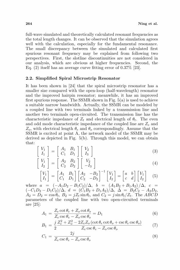
full-wave simulated and theoretically calculated resonant frequencies asthe total length changes. It can be observed that the simulation agreeswell with the calculation, especially for the fundamental resonance.The small discrepancy between the simulated and calculated firstspurious resonant frequency may be explained from following twoperspectives. First, the slotline discontinuities are not considered inour analysis, which are obvious at higher frequencies. Second, theEq. (2) itself has an average curve fitting error of 0.37% [23].
2.2. Simplified Spiral Microstrip Resonator
It has been shown in [24] that the spiral microstrip resonator has asmaller size compared with the open-loop (half-wavelength) resonatorand the improved hairpin resonator; meanwhile, it has an improvedfirst spurious response. The SSMR shown in Fig. 5(a) is used to achievea suitable narrow bandwidth. Actually, the SSMR can be modeled bya coupled line with two terminals linked by a transmission line andanother two terminals open-circuited. The transmission line has thecharacteristic impedance of Zt and electrical length of θt. The evenand odd mode characteristic impedance of the coupled line are Ze andZo, with electrical length θe and θo correspondingly. Assume that theSSMR is excited at point A, the network model of the SSMR may bederived as depicted in Fig. 5(b). Through this model, we can obtainthat: [
V1
I1
]=
[A1 B1
C1 D1
] [V2
I3
](3)
[V1
I2
]=
[A2 B2
C2 D2
] [V2
−I3
](4)
[V1
I1
]=
[A1 B1
C1 D1
] [A2 −B2
C2 −D2
]−1 [V1
I2
]=
[a bc d
] [V1
I2
](5)
where a = (−A1D2 −B1C2)/∆, b = (A1B2 + B1A2) /∆, c =(−C1D2 −D1C2)/∆, d = (C1B2 + D1A2)/∆, ∆ = B2C2 − A2D2,A2 = D2 = cos θt, B2 = jZt sin θt, and C2 = j sin θt/Zt. The ABCDparameters of the coupled line with two open-circuited terminalsare [25]:
A1 =Ze cot θe + Zo cot θo
Ze csc θe − Zo csc θo= D1 (6)
B1 =j
2Z2
e + Z2o − 2ZeZo (cot θe cot θo + csc θe csc θo)
Ze csc θe − Zo csc θo(7)
C1 =2j
Ze csc θe − Zo csc θo(8)

Progress In Electromagnetics Research, Vol. 131, 2012 265
Then, the input impedance ZI is expressed as:
ZI =V1
II=
V1
I1 + I2=
b
bc + (1− a) (1 + d)(9)
The resonance will happen when I1 = −I2 (i.e., ZI = ∞). Fig. 6shows the full-wave simulated and calculated fundamental and firstspurious resonant frequencies (denoted by f2 and fs2), as well as theirratio against the length S3. It can be clearly seen that the simulationsin Fig. 6(a) agree well with the calculations in Fig. 6(b), demonstratingthe validity of our analysis. As the length S3 increases, the fundamentalresonant frequency decreases while the variation of the first spuriousresonance is very small or even neglected. Therefore, the ratio of thefirst spurious resonant frequency to the fundamental one is increased.Compared with the conventional half-wavelength resonator with thefirst spurious resonance at 2f2, the improved first spurious resonancecan be easily achieved for the SSMR. It is worth pointing out that dueto the internal coupling of the SSMR, the fundamental resonance ofthis resonator will be lower than that of the half-wavelength resonatorwith the same length, meaning that the SSMR is more compact.For instance, the fundamental resonance of the SSMR is located at3.24GHz when the length S3 is 4.4 mm; while for the half-wavelengthresonator with the same length of the SSMR, the fundamental resonantfrequency is only 3.84 GHz.
2S
1S
ws
4S3S
2 2
2 2
A B
C D
1 1
1 1
A B
C D1V
1V
1I
2I
1V
II
2V
2V
3I
3I
IZ
(a) (b)
ACoupled
Line
-
[
[
[
[
Figure 5. (a) Simplified spiral microstrip resonator. (b) Networkmodel.

266 Ning et al.
2.0 2.5 3.0 3.5 4.0 4.52
4
6
8
10
2 2sf f2sf
3S
2f
Length, (mm)
Fre
qu
ency
(G
Hz)
1.9
2.2
2.5
2.8
3.1
Ra
tio
2.0 2.5 3.0 3.5 4.0 4.52
4
6
8
10
2 2sf f2sf
3S
2f
Length, (mm)
Fre
qu
ency
(G
Hz)
1.9
2.2
2.5
2.8
3.1
Ra
tio
(b)(a)
Figure 6. (a) Full-wave simulated and (b) calculated fundamentaland first spurious resonant frequencies of SSMR, as well as their ratioagainst the length S3 (S1 = 7.0 mm, S2 = 5.3 mm, S3 = 4.4mm,S4 = 6.2mm, ws = 0.4mm).
3. DUAL NARROW-BAND BANDSTOP FILTERIMPLEMENTATION
Based on the aforementioned analysis, the MS-DMSs can be used torealize one stopband, and the SSMRs coupled to the main microstripline may be utilized to implement another stopband. To achievecompactness, the first stopband is determined by the MS-DMS andthe second stopband depends on the SSMR. Thus, a dual narrow-band bandstop filter is constructed and its configuration is depictedin Fig. 7. It is noted that these two stopbands can be individuallycontrolled and separately designed since they are generated throughdifferent resonators and current paths. Meanwhile, the first spuriousresonance fs of this filter can be approximately estimated as:
fs ≈ min fs1, fs2 fs1 ≈ 3f1, fs2 > 2f2 (10)As for the stopband design using the SSMRs coupled to the main
microstrip line, the conventional design methodology of narrow-bandbandstop filter [26] may be applied. The equivalent circuit model forthis kind of filter design is illustrated in Fig. 8 and the design flow isoutlined as follows. The first step is circuit synthesis, which is basedon the operated frequency f0 and 3-dB fractional bandwidth (FBW).The design parameters are obtained by:
(YU
Y0
)2
=1
g0gn+1(11)
(bi
Y0
)=
(YU
Y0
)2 g0
giΩcFBW=
f0
2∆f3 dBifor i = 1 to n (12)

Progress In Electromagnetics Research, Vol. 131, 2012 267
bi = 2πf0Ci =1
2πf0Lifor i = 1 to n (13)
where Y0 and YU denote the terminating admittance and characteristicadmittance of immittance inverters; gi are the element values oflowpass prototype; Ωc is the normalized cutoff frequency; bi and ∆f3 dBi
are the susceptance slop parameters and 3-dB bandwidths of theserials parallel resonators correspondingly; Li and Ci are the equivalentinductances and capacitances of each resonator respectively.
The second step is to use the SSMRs with different coupling spacesdi to the main microstrip line to meet the required susceptance slopparameters. For simplicity, the SSMRs’ dimensions are chosen as thesame to make them have the same fundamental and first spuriousresonant frequency, and the desired coupling space can be obtainedwith the aid of a full-wave EM solver.
It is worth mentioning that if the radiation loss and conductorloss of the proposed MS-DMS are neglected, its transmission responsecan be expressed by a parallel LC resonant circuit. Concurrently,the MS-DMS has a high-Q factor. Hence, the above discussed designmethodology can be also applied to implement another stopband designusing the MS-DMSs if we can obtain proper dimensions of each MS-DMS unit cell to satisfy the required normalized susceptance slop
s
1d 2d 3d
2uS
1uS
3uS4uS
1l
ws
Figure 7. Configuration of the dual narrow-band bandstop filter.
1C
1L
nC
2C
2L
nL
UY
90
0Y
0Y
o
Figure 8. Equivalent circuit model for the narrow-band bandstopfilter design.

268 Ning et al.
0.90 0.95 1.00 1.05 1.10-30
-20
-10
0
M3=2.2 mm
M3=2.8 mm
M3=3.4 mm
1f f
| S21
| (d
B)
Figure 9. Effects of the MS-DMS width M3 on the stopbandbandwidth (w1 = 0.3mm, M1 = 9mm, M2 = 8.4mm, M4 = 0.3mm).
21S
11S
0 1 2 3 4 5 6-50
-40
-30
-20
-10
0
Full-wave
Circuit
Ma
gn
itu
de
(dB
)
Frequency (GHz)
s
Figure 10. Circuit and full-wave simulated responses of the designedsecond-order filter using MS-DMSs (W = 4.4mm, w1 = 0.25mm,M1 = 11.3mm, M2 = 10.7mm, M3 = 2.0 mm, M4 = 0.3mm,s = 22.3 mm, L1 = L2 = 5.87 nH, C1 = C2 = 0.75 pF).
parameter of each resonator. Based on the full-wave simulations, it isfound that: the stopband bandwidth of the MS-DMS could be adjustedby tuning the width M3, while the length M1 and M2 have little effecton the bandwidth and the resonant frequency mainly depends on that.The simulated transmission responses of the MS-DMS with differentwidths M3 are shown in Fig. 9, where the 3-dB FBW of the stopbandincreases from 5.3% to 11.2% when the width M3 varies from 2.2mm to3.4mm. Therefore, by finely tuning the dimensions of MS-DMS withthe help of a full-wave EM solver, the desired normalized susceptanceslop parameter can be achieved. We should remember that the designrule of the MS-DMS discussed in Subsection 2.1 will make this processmore efficient.

Progress In Electromagnetics Research, Vol. 131, 2012 269
As an illustrative example of the bandstop filter design using theMS-DMSs, a simple second-order filter with the center frequency of2.4GHz and 3-dB FBW of 6.25% is designed following the aboveprocedure. A two-pole Butterworth lowpass prototype is used withthe element values g0 = g3 = 1.0, g1 = g2 = 1.4142 at Ωc = 1. UsingEq. (12), we can yield the desired design parameters as:
YU = Y0, b1/Y0 = b2/Y0 = 8.0 (14)
Thus, the two MS-DMS unit cells should have the same dimensions.The layout of this designed filter along with its final dimensions isshown in Fig. 10. The full-wave and circuit simulated responses ofthis filter are also plotted in Fig. 10 and a good agreement is obtainedbetween the two. The small difference in the rejection level of thecenter frequency of the stopband and the reflection coefficient at higherfrequencies results from the radiation loss caused by the MS-DMSs.
Figure 11. Photograph of the fabricated dual narrow-band bandstopfilter. (S1u = 7.0mm, S2u = 5.3mm, S3u = 4.0mm, S4u = 5.7mm,ws = 0.4mm, d1 = d3 = 0.2mm, d2 = 0.15mm, l1 = 15.2mm, otherdimensions are the same with that in Fig. 10).
0 1 2 3 4 5 6 7 8-50
-40
-30
-20
-10
0
Measurement
Simulation
|S2
1| (
dB
)
Frequency (GHz)
1f
2f
sf
0 1 2 3 4 5 6 7 8-50
-40
-30
-20
-10
0
Measurement
Simulation
|S1
1| (
dB
)
Frequency (GHz)
Figure 12. Simulated and measured responses of the fabricated dualnarrow-band bandstop filter.

270 Ning et al.
A dual narrow-band bandstop filter is designed according to abovedesign process and simulated by HFSS. The final optimized filter isfabricated on Arlon Cuclad 250 GX(tm) substrate with a relativedielectric constant of 2.55, a thickness of 1.5mm, and a loss tangentof 0.002. Fig. 11 shows the photograph of the fabricated filter and thesimulated and measured responses of this filter are depicted in Fig. 12,showing a good agreement between the two. Some slight discrepanciesmay be attributed to the fabrication error.
As can be seen in Fig. 12, the measured dual stopbandsare centered at 2.37 GHz and 3.54GHz, with 3-dB FBWs of6.33% (2.29 GHz–2.44 GHz) and 3.39% (3.48 GHz–3.60GHz), stopbandrejections of 31.4 dB and 36.7 dB respectively. The first spuriousresonance is located at 7.52 GHz (i.e., 3.17f1). The measured typicalinsertion loss of the low, middle and upper passband (below 7.52 GHz)is 0.12 dB, 0.40 dB and 0.82 dB correspondingly. The measured returnloss is better than 11.5 dB in the whole passbands. It is noticed thatdue to the utilization of the MS-DMSs, the proposed dual narrow-bandbandstop filter is more compact compared with the filter in [12], whichalso has two independently controlled stopbands. Moreover, unlikethe quarter-wavelength resonator filters [13] with the first spuriousresonance located at 3f1, the improved spurious response of theproposed filter is achieved without needing short-circuit connectionsto ground through via holes, which makes this filter quite compatiblewith planar fabrication techniques.
4. TRIPLE NARROW-BAND BANDSTOP FILTERIMPLEMENTATION
Based on above investigations, a third stopband can be generatedby simultaneously adding the SSMRs to another side of the mainmicrostrip line of the dual narrow-band bandstop filter. Therefore, atriple narrow-band bandstop filter is constructed and Fig. 13(a) showsits layout. Through this configuration, the triple stopbands can beindividually controlled, and the first spurious resonance fs of this filtermay be roughly obtained as:
fs ≈ min fs1, fs2, fs3 fs1 ≈ 3f1, fs2 > 2f2, fs3 > 2f3 (15)
where f3 is the third fundamental resonant frequency caused by theadded SSMR, and fs3 is its first spurious resonant frequency.
A triple narrow-band bandstop filter is designed, simulated andmeasured to verify the proposed design method. The fabricated filteralong with its dimensions is shown in Fig. 13(b). The simulatedand measured responses of this filter are plotted in Fig. 14 and a

Progress In Electromagnetics Research, Vol. 131, 2012 271
good agreement is obtained. Both the simulation and measurementshow that the triple stopbands are located at 2.37 GHz, 3.54 GHz,and 5.01GHz, with 3-dB FBWs of 6.33% (2.29GHz–2.44 GHz),3.95% (3.47 GHz–3.61 GHz) and 3.79% (4.93 GHz–5.12GHz), stopbandrejections of 31.2 dB, 30.9 dB and 40.5 dB correspondingly. The firstspurious resonant frequency is 7.52 GHz equal to 3.17f1. Thus, theimproved spurious response of this filter is obtained. The measuredtypical insertion losses of the four passbands, which are from lowerfrequency to higher frequency and below the first spurious resonantfrequency, are 0.14 dB, 0.35 dB, 0.50 dB and 0.92 dB respectively. Thereturn loss is better than 10 dB in the whole passbands. It should benoted that the first and second stopband as well as the first spuriousresonance of this triple-band filter are almost the same with theaforementioned dual-band filter, further demonstrating our proposeddesign concept.
2l
2dS
1dS
3dS4dS
4d 5d 6d
(a) (b)
Figure 13. (a) Layout of the triple narrow-band bandstop filter.(b) Photograph of the fabricated filter (S1d = 5.3mm, S2d = 4.3mm,S3d = 2.7mm, S4d = 4.2mm, d4 = d6 = 0.24mm, d5 = 0.2mm,l2 = 10.4mm, other dimensions are the same as that in Fig. 11).
0 1 2 3 4 5 6 7 8-50
-40
-30
-20
-10
0
Measurement
Simulation
|S21
|(d
B)
Frequency (GHz)
1f
2f
3f
sf
0 1 2 3 4 5 6 7 8-50
-40
-30
-20
-10
0
Measurement
Simulation
|S1
1|(d
B)
Frequency (GHz)
Figure 14. Simulated and measured responses of the fabricated triplenarrow-band bandstop filter.

272 Ning et al.
5. CONCLUSION
This paper presents a new design method of planar dual and triplenarrow-band bandstop filter. First, the fundamental and the firstresonant frequencies of the proposed MS-DMS are analyzed fromthe perspective of EM wave propagation, and the resonances of theSSMR are discussed based on its network model. Second, by makinguse of the characteristics of the MS-DMS and the SSMR coupled tothe main microstrip line, a dual and triple narrow-band bandstopfilter are implemented, which have independently controlled stopbandsand improved first spurious resonance. Both the simulation andmeasurement of the fabricated filters validate our proposed designconcept, and show good passband performance and stopband rejection.Easy to design and fabricate, the developed filters can be a goodcandidate for the application of multi-band wireless communicationsystems.
ACKNOWLEDGMENT
This work is jointly funded by the National Natural Science Foundationof China (NSFC) and Civil Aviation Administration of China (CAAC)(61079019).
REFERENCES
1. Yang, R.-Y., K. Hon, C.-Y. Hung, and C.-S. Ye, “Design of dual-band bandpass filters using a dual feeding structure and embeddeduniform impedance resonators,” Progress In ElectromagneticResearch, Vol. 105, 93–102, 2010.
2. Ma, D.-C., Z.-Y. Xiao, L.-L. Xiang, X.-H. Wu, C.-Y. Huang, andX. Kou, “Compact dual-band bandpass filter using folded SIRwith two stubs for WLAN,” Progress In Electromagnetic Research,Vol. 117, 357–364, 2011.
3. Chaudhary, G., Y. Jeong, K. Kim, and D. Ahn, “Design ofdual-band bandpass filters with controllable bandwidths usingnew mapping function,” Progress In Electromagnetic Research,Vol. 124, 17–34, 2012.
4. Chiou, Y.-C. and J.-Y. Kuo, “Planar multiband bandpass filterwith multimode stepped-impedance resonators,” Progress InElectromagnetic Research, Vol. 114, 129–144, 2011.
5. Chen, J., J.-Z. Chen, B. Wu, Y. L. Zhang, and C.-H. Liang,“Design of triple-band microstrip filter with transmission zeros

Progress In Electromagnetics Research, Vol. 131, 2012 273
using open stubs,” Journal of Electromagnetic Waves andApplication, Vol. 26, No. 4, 525–534, 2012.
6. Chen, W.-Y., M.-H. Weng, S.-J. Chang, H. Kuan, and Y.-H. Su, “A new tri-band bandpass filter for GSM, WiMAX, andultra-wideband responses by using asymmetric stepped impedanceresonators,” Progress In Electromagnetic Research, Vol. 124, 365–381, 2012.
7. Uchida, H., H. Kamino, K. Totani, N. Yoneda, M. Miyazaki,Y. Konishi, S. Makino, J. Hirokawa, and M. Ando, “Dual-band-rejection filter for distortion reduction in RF transmitters,” IEEETrans. Microwave Theory Tech., Vol. 52, No. 11, 2550–2556, 2004.
8. Tseng, C.-H. and T. Itoh, “Dual-band bandpass and bandstop fil-ters using composite right/left-handed metamaterial transmissionlines,” IEEE MTT-S Int. Microwave Symp. Dig., 931–934, 2006.
9. Chin, K.-S., J. H. Yeh, and S. H. Chao, “Compact dual-band bandstop filters using stepped-impedance resonators,” IEEEMicrowave Wireless Comp. Lett., Vol. 17, No. 12, 849–851, 2007.
10. Chin, K.-S. and C.-K. Lung, “Miniaturized microstrip dual-bandbandstop filters using tri-section stepped-impedance resonators,”Progress In Electromagnetic Research C, Vol. 10, 37–48, 2009
11. Cheng, D., H.-C. Yin, and H.-X. Zheng, “A compact dual-band bandstop filter with defected microstrip slot,” Journal ofElectromagnetic Waves and Application, Vol. 26, No. 10, 1374–1380, 2012.
12. Vegesna, S. and M. Saed, “Microstrip dual-band bandpass andbandstop filters,” Microwave Opt. Technol. Lett., Vol. 54, No. 1,168–171, 2012.
13. Rambabu, K., M. Y.-W. Chia, K. Chan, and J. Bornemann,“Design of multiple-stopband filters for interference suppressionin UWB applications,” IEEE Trans. Microwave Theory Tech.,Vol. 58, No. 8, 3333–3338, 2006.
14. Han, S. H., X. L. Wang, and Y. Fan, “Analysis and designof multiple-band bandstop filters,” Progress In ElectromagneticResearch, Vol. 70, 297–306, 2007.
15. Wang, Y., J. Zhou, and W. Hong, “A multiband bandstop filtersusing a single ring resonator for a wireless access communicationsystem,” Microwave Journal, Vol. 54, No. 3, 102–108, 2011.
16. Kazerooni, M. and A. Cheldavi, “Simulation, analysis, design andapplications of array defected microstrip structure (ADMS) filtersusing rigorously coupled multi-strip (RCMS) method,” ProgressIn Electromagnetic Research, Vol. 63, 193–207, 2006.

274 Ning et al.
17. Fallahzadeh, S. and M. Tayarani, “A new microstrip UWBbandpass filter using defected microstrip structures,” Journal ofElectromagnetic Waves and Application, Vol. 24, No. 7, 893–902,2010.
18. Barbarino, S. and F. Consoli, “UWB circular slot antennaprovided with an inverted-L notch filter for the 5 GHz WLANband,” Progress In Electromagnetic Research, Vol. 104, 1–13,2010.
19. Xiang, Q.-Y., Q.-Y. Feng, and X.-G. Huang, “Bandstop filterbased on complementary split ring resonators defected microstripstructure,” Journal of Electromagnetic Waves and Application,Vol. 25, No. 13, 1895–1908, 2011.
20. La, D., Y. Lu, S. Sun, N. Liu, and J. Zhang, “A novel compactbandstop filter using defected microstrip structure,” MicrowaveOpt. Technol. Lett., Vol. 53, No. 2, 433–435, 2011.
21. Kazerooni, M. and M. Aghalari, “Size reduction and harmonicsuppression of rat-race hybrid coupler using defected microstripstructure,” Progress In Electromagnetic Research Letters, Vol. 26,87–96, 2011.
22. Cheng, D., H.-C. Yin, and H.-X. Zheng, “Investigation ona defected microstrip structure and applications in designingmicrostrip filters,” Journal of Electromagnetic Waves andApplication, Vol. 26, No. 10, 1332–1340, 2012.
23. Gupta, K. C., R. Garg, I. Bahl, and P. Bhartia, Microstrip Linesand Slotlines, 2nd Edition, Artech House, Norwood, MA, 1996.
24. Joubert, J., “Spiral microstrip resonators for narrow-stopbandfilters,” IEE Proc.-Microwave Antennas Propag., Vol. 150, No. 6,493–496, 2003.
25. Zysman, G. I. and A. Johnson, “Coupled transmission linenetworks in an inhomogeneous dielectric medium,” IEEE Trans.Microwave Theory Tech., Vol. 17, No. 10, 753–759, 1969.
26. Hong, J. S. and M. J. Lancaster, Microstrip Filters forRF/Microwave Applications, John Wiley & Sons, New York, 2001.