![A phase shifted full bridge converter design for ... · [3] gives the design methodology to reach high efficiency and decreased volume. In [4], integrated on-board chargers are discussed.](https://static.fdocuments.in/doc/165x107/5f7228406b8e7c764b493fd4/a-phase-shifted-full-bridge-converter-design-for-3-gives-the-design-methodology.jpg)
Design of Phase Shifted Full-Bridge Converter with Current ... export/supplier...
20
Design Note DN 2013-01 V1.0 January 2013 Design of Phase Shifted Full-Bridge Converter with Current Doubler Rectifier Sam Abdel-Rahman Infineon Technologies North America (IFNA) Corp.
Transcript of Design of Phase Shifted Full-Bridge Converter with Current ... export/supplier...

Design Note DN 2013-01
V1.0 January 2013
Design of Phase Shifted Full-Bridge
Converter with Current Doubler Rectifier
Sam Abdel-Rahman
Infineon Technologies North America (IFNA) Corp.

Design of Phase Shifted Full-Bridge Converter with Current Doubler Rectifier
2
Design Note DN 2013-01
V1.0 January 2013
Published by Infineon Technologies North America 27703 Emperor Blvd, suite 310 Durham, NC 27703 All Rights Reserved.
Attention please!
THE INFORMATION GIVEN IN THIS APPLICATION NOTE IS GIVEN AS A HINT FOR THE IMPLEMEN-TATION OF THE INFINEON TECHNOLOGIES COMPONENT ONLY AND SHALL NOT BE REGARDED AS ANY DESCRIPTION OR WARRANTY OF A CERTAIN FUNCTIONALITY, CONDITION OR QUALITY OF THE INFINEON TECHNOLOGIES COMPONENT. THE RECIPIENT OF THIS APPLICATION NOTE MUST VERIFY ANY FUNCTION DESCRIBED HEREIN IN THE REAL APPLICATION. INFINEON TECHNOLOGIES HEREBY DISCLAIMS ANY AND ALL WARRANTIES AND LIABILITIES OF ANY KIND (INCLUDING WITHOUT LIMITATION WARRANTIES OF NON-INFRINGEMENT OF INTELLECTUAL PROPERTY RIGHTS OF ANY THIRD PARTY) WITH RESPECT TO ANY AND ALL INFORMATION GIVEN IN THIS APPLICATION NOTE.
Information
For further information on technology, delivery terms and conditions and prices please contact your
nearest Infineon Technologies Office (www.infineon.com).
Warnings
Due to technical requirements components may contain dangerous substances. For information on the
types in question please contact your nearest Infineon Technologies Office. Infineon Technologies
Components may only be used in life-support devices or systems with the express written approval of
Infineon Technologies, if a failure of such components can reasonably be expected to cause the failure of
that life-support device or system, or to affect the safety or effectiveness of that device or system. Life
support devices or systems are intended to be implanted in the human body, or to support and/or maintain
and sustain and/or protect human life. If they fail, it is reasonable to assume that the health of the user or
other persons may be endangered.
AN 2013-01 Subjects: Design of Phase Shifted Full-Bridge Converter with Current Doubler Rectifier
Author: Sam Abdel-Rahman (IFNA PMM SMD AMR PMD 2) We Listen to Your Comments
Any information within this document that you feel is wrong, unclear or missing at all? Your feedback will help us to continuously improve the quality of this document. Please send your proposal (including a reference to this document) to: [[email protected]]

Design of Phase Shifted Full-Bridge Converter with Current Doubler Rectifier
3
Design Note DN 2013-01
V1.0 January 2013
Table of contents
1 Introduction .................................................................................................................................................. 4
2 Full-Bridge Converter with Current Doubler Rectifier ............................................................................. 4
3 Modes of Operation ..................................................................................................................................... 5
4 Energy and Deadtime Conditions for Acheiving ZVS .............................................................................. 8
5 Design Equations and Power Losses ..................................................................................................... 10
6 References ................................................................................................................................................. 19

Design of Phase Shifted Full-Bridge Converter with Current Doubler Rectifier
4
Design Note DN 2013-01
V1.0 January 2013
1 Introduction
While the front-end stage of an AC/DC rectifier achieves power factor correction and regulates the bus voltage to a dc value (~390V), the dc-dc stage must step down the bus voltage and provide a galvanically isolated and tightly regulated dc output (eg. 12V, 24V, 48V). This document is intended to discuss the topology and operation of the dc-dc stage for medium to high power applications ( >400W), and provide detailed design equations with examples.
A wide range of isolated topologies are available for the dc-dc stage, but the choice depends primarily on power level, complexity and cost. Ideally it is desired to select the topology with the least cost and complexity, nevertheless, one that can handle the power level with reliable and acceptable performance.
Figure 1.1 shows a chart for topology selection, it must be noted that topologies in this chart are not necessarily limited to the indicated power ranges, the intention of the chart is only to illustrate topologies power handling and their common application, relatively.
Figure 1.1
2 Full-Bridge Converter with Current Doubler Rectifier
According to specifications in Table 1 and the chart above, 600W could be realized with either a half-bridge or full-bridge. 600W falls in the high end of the half-bridge power handling range, while a full-bridge can handle that power with less stress and better performance. A full-bridge has half the rms current compared to a half-bridge, also, it can be implemented with phase shift control which provides Zero Voltage Switching (ZVS) for primary side switches.
Since the output is 12V and 50A, current double rectifier with synchronous rectification (Figure 2.1) is the most suitable for such high current application, as it splits the output current between two filter inductors, which reduces conduction losses, improves thermal distribution, and allows for lower profile, in addition to the ripple cancellation effect on the output capacitance.
Table 1 Specifications
Input voltage 390 V
Output voltage 12 V
Maximum power 600 W
Switching frequency 200 kHz
Inductor current ripple 20%
Output capacitor voltage ripple 12 mVp-p

Design of Phase Shifted Full-Bridge Converter with Current Doubler Rectifier
5
Design Note DN 2013-01
V1.0 January 2013
Figure 2.1
3 Modes of Operation
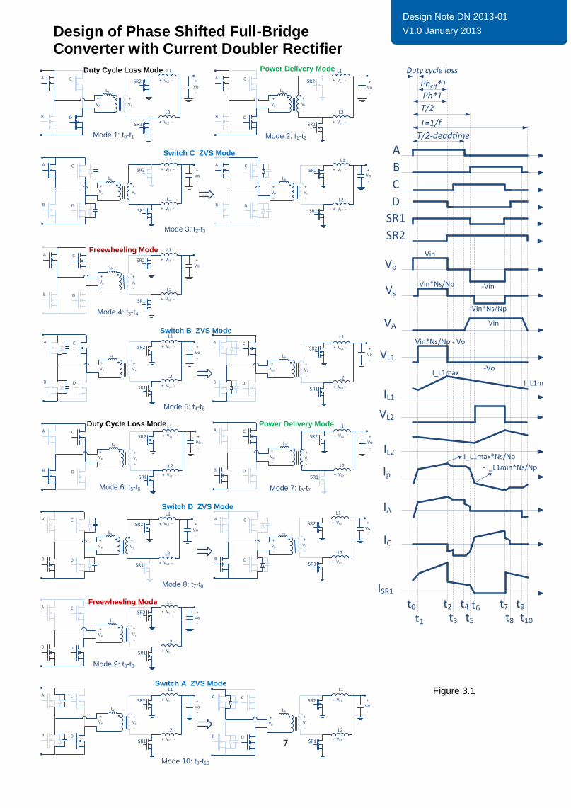
Figure 3.1 shows the equivalent circuit of each mode and key waveforms, switches A and B are switched complimentary with 50% duty cycle minus a short dead time, switches C and D are also switched complimentary with 50% duty cycle minus a short dead time, phase shift control between the two switches pairs A,B and C,D is used for output voltage regulation.
Mode 1: (t0-t1)
Duty Cycle Loss Mode
At t=t0, switch A is turned on with ZVS (as a consequence of Mode 10 below), transformer secondary voltage Vs will remain zero and both secondary side rectifiers SR1 and SR2 will remain conducting current eventhough that SR2 is gated off, both inductors L1 and L2 are discharging, secondary voltage Vs remain zero until the primary current Ip reverses its direction and rise to reach the reflected output inductor current IL1*Ns/Np at t=t1. Ip rises with a slope as the input voltage Vin charges the leakage inductor Lk, and SR2 current slopes down to reach zero at t=t1. No power is delivered to the output in this mode.
Mode 2: (t1-t2)
Power Delivery Mode
At t=t1, the transformer secondary voltage Vs is equal to Vin*Ns/Np, the output inductor L1 is charging, the output inductor L2 is discharging, SR1 carries both inductors current. The effective phase shift Pheff starts in this mode. The primary winding current Ip is equal to the reflected output inductor current IL1*Ns/Np.
Mode 3: (t2-t3)
Switch C ZVS Mode
At t=t2, switch D is turned off, the primary current Ip charges the capacitance of switch D and discharges the capacitance of switch C. when switch C is discharged to zero, its body diode conducts to achieve zero voltage switching condition, the transformer secondary voltage Vs becomes zero and both SR’s carry current.
ACPFC
ConverterDC/DC
ConverterLoad
DC Bus
Vac+
Vo-
A
B
C
D
SR2
SR1
+Vp
-
+Vo-
L1
L2
+ VL1 -
+ VL2 -
Lk
+Vs
-
DC Bus
Ip
IL1
IL2
IA IC
+VA
-
ISR1
ISR2

Design of Phase Shifted Full-Bridge Converter with Current Doubler Rectifier
6
Design Note DN 2013-01
V1.0 January 2013
Mode 4: (t3-t4)
Freewheeling Mode
At t=t3, switch C is turned on with ZVS, current Ip freewheels through switches A and C, the transformer secondary voltage Vs is zero, inductor L1 discharges by the output voltage through SR2, and inductor L2 discharges through SR1.
Mode 5: (t4-t5)
Switch B ZVS Mode
At t=t4, switch A is turned off, the primary current charges the capacitance of switch A and discharges the capacitance of switch B. when switch B is discharged to zero, its body diode conducts to achieve zero voltage switching condition, the transformer secondary voltage Vs remains zero and both SR’s keeps conducting.
Mode 6: (t5-t6)
Duty Cycle Loss Mode
At t=t5, switch B is turned on with ZVS, transformer secondary voltage Vs will remain zero and both secondary side rectifiers SR1 and SR2 will remain conducting current eventhough that SR1 is gated off, Bothe inductors L1 and L2 are discharging. secondary voltage Vs remain zero until the current Ip reverses its direction and rise (in the negative direction) to reach the reflected output inductor current IL2*Ns/Np at t=t6. Ip changes with a slope as the input voltage Vin discharges the leakage inductor Lk, and SR1 current slopes down to reach zero at t=t6. No power is delivered to the output in this mode.
Mode 7: (t6-t7)
Power Delivery Mode
At t=t6, the transformer secondary voltage Vs is equal to Vin*Ns/Np, the output inductor L2 is charging, the output inductor L1 is discharging, SR2 carries both inductors current. The effective phase shift Pheff starts again in this mode. The primary current Ip (in the negative direction) is equal to the reflected output inductor current IL2*Ns/Np.
Mode 8: (t7-t8)
Switch D ZVS Mode
At t=t7, switch C is turned off, the primary current Ip charges the capacitance of switch C and discharges the capacitance of switch D. when switch D is discharged to zero, its body diode conducts to achieve zero voltage switching condition, the transformer secondary voltage Vs becomes zero and both SR’s carry current.
Mode 9: (t8-t9)
Freewheeling Mode
At t=t8, switch D is turned on with ZVS, current Ip freewheels through switches B and D, the transformer secondary voltage Vs is zero, inductor L1 discharges by the output voltage through SR2, and inductor L2 discharges through SR1.
Mode 10: (t9-t10)
Switch A ZVS Mode
At t=t9, switch B is turned off, the primary current Ip charges the capacitance of switch B and discharges the capacitance of switch A. when switch A is discharged to zero, its body diode conducts to achieve zero voltage switching condition, the transformer secondary voltage Vs remains zero and both SR’s keeps carrying current.
Design of Phase Shifted Full-Bridge Converter with Current Doubler Rectifier
7
Design Note DN 2013-01
V1.0 January 2013
Figure 3.1
A
B
C
D
+Vp
-
A
B
C
D
+Vp
-
A
B
C
D
+Vp
-
A
B
C
D
+Vp
-
A
B
C
D
+Vp
-
A
B
C
D
+Vp
-
A
B
C
D
+Vp
-
A
B
C
D
+Vp
-
Lk
Lk Lk
Lk
Lk
Lk
Lk
Lk
SR2
SR1
+Vo-
L2
+ VL1 -
+ VL2 -
+Vs
-
SR2
SR1
+Vo-
L2
+ VL1 -
+ VL2 -
+Vs
-
SR2
SR1
+Vo-
L2
+ VL1 -
+ VL2 -
+Vs
-
SR2
SR1
+Vo-
L2
+ VL1 -
+ VL2 -
+Vs
-
A
B
C
D
+Vp
-
Lk
A
B
C
D
+Vp
-
Lk
SR2
SR1
+Vo-
L2
+ VL1 -
+ VL2 -
+Vs
-
A
B
C
D
+Vp
-
Lk
A
B
C
D
+Vp
-
Lk
SR2
SR1
+Vo-
L2
+ VL1 -
+ VL2 -
+Vs
-
SR2
SR1
+Vo-
L2
+ VL1 -
+ VL2 -
+Vs
-
SR2
SR1
+Vo-
L2
+ VL1 -
+ VL2 -
+Vs
-
SR2
SR1
+Vo-
L2
+ VL1 -
+ VL2 -
+Vs
-
SR2
SR1
+Vo-
L2
+ VL1 -
+ VL2 -
+Vs
-
A
B
C
D
+Vp
-
Lk
Mode 1: t0-t1
SR2
SR1
+Vo-
L2
+ VL1 -
+ VL2 -
+Vs
-
SR2
SR1
+Vo-
L2
+ VL1 -
+ VL2 -
+Vs
-
SR2
SR1
+Vo-
L2
+ VL1 -
+ VL2 -
+Vs
-
A
B
C
D
+Vp
-
Lk
SR2
SR1
+Vo-
L2
+ VL1 -
+ VL2 -
+Vs
-
Mode 2: t1-t2
Mode 3: t2-t3
Mode 4: t3-t4
Mode 6: t5-t6 Mode 7: t6-t7
Mode 9: t8-t9
Mode 10: t9-t10
Mode 8: t7-t8
Mode 5: t4-t5
L1 L1
L1 L1
L1 L1
L1
L1 L1
L1L1
L1
L1L1
Power Delivery Mode
Power Delivery Mode
Freewheeling Mode
Freewheeling Mode
Switch B ZVS Mode
Switch D ZVS Mode
Switch A ZVS Mode
Switch C ZVS Mode
Duty Cycle Loss Mode
Duty Cycle Loss Mode
A
B
Vp
VA
VL1
IL1
IA
IC
ISR1
T=1/f
Ph*T
T/2
Vin
-Vin
Vin
Vin*Ns/Np - Vo
-VoI_L1max
I_L1min
C
D
T/2-deadtime
VL2
IL2I_L1max*Ns/Np
Ip- I_L1min*Ns/Np
t1
t2
t3
t4
t5
t6 t7
t8
SR1
SR2
t9
t10
VsVin*Ns/Np
-Vin*Ns/Np
t0
Pheff*T
Duty cycle loss

Design of Phase Shifted Full-Bridge Converter with Current Doubler Rectifier
8
Design Note DN 2013-01
V1.0 January 2013
4 Energy and Deadtime Conditions for Acheiving ZVS
Although Figure 3.1 shows ZVS turn on for all primary side switches, ZVS may be lost partially or completely due to lack of energy or insufficient deadtime.
During no load and light load conditions, ZVS may be lost if the inductive energy available in the circuit is not sufficient to charge and discharge the output capacitance of the two FETs in the same bridge leg in addition to the transformer capacitance.
The Energy condition for achieving ZVS is:
The total capacitive energy in the switching leg and transformer is:
Where is the transformer capacitance, and is the MOSFET’s equivalent energy related output
capacitance as list in the datasheet, below is an example from the IPW65R310CFD datasheet to show the parameter and its definition.
The inductive energy available for ZVS for switches C and D is higher than that for switches A and B. For that reason, switches C and D have a wider ZVS range compared to switches A and B.
In regards to ZVS for both switches C and D, it can be seen in the equivalent circuits of modes 3 and 8 (Figure 3.1) that leakage inductor, magnetizing inductor and reflected inductor all contribute to the ZVS available energy, therefore, the total inductive energy available for ZVS for switches C and D is:
Where is the magnetizing inductor and is its peak current.
However, in regards to ZVS for both switches A and B, it can be seen in the equivalent circuits of modes 5 and 10 (Figure 3.1) that the transformer is clamped to zero voltage, and both output inductors currents freewheels in the SRs, hence the leakage inductor is the only inductive energy source available for ZVS, therefore, the total inductive energy available for ZVS for both switches A and B is:
Since the magnetizing energy is not a function of the load current, the designer could slightly gap the transformer core, in order to tune the magnetizing energy such that ZVS range of is extended at light loads conditions. Another design practice used to extend the ZVS range is to add an external leakage inductor in series with the transformer primary, which adds to the leakage energy.
Besides having sufficient energy for achieving ZVS, the deadtime must also be enough to make the voltage transition, which is dependent on the resonant circuit parameters. Figure 4.1 shows a simple illustration of the ZVS transition during deadtime, it is seent that the voltage (Vds) transitions to zero in a resonant manner with a resonant frequency equal to fr, therefore the Vds requires at least one forth of the resonant period (Tr/4) to complete the transition. Deadtime below Tr/4 will cause switching at a non-zero voltage (partial ZVS), on the other hand, deadtime higher than Tr/4 will cause extra body diode conduction losses, furthermore, might cause losing ZVS if the resonant circuit is highly damped (or lossy).

Design of Phase Shifted Full-Bridge Converter with Current Doubler Rectifier
9
Design Note DN 2013-01
V1.0 January 2013
Figure 4.1
Figure 4.2 shows the circuit for the ZVS mode of switch C (Mode 3) and its equivalent resonant circuit, the equivalent resonant circuit is similar for all other ZVS transition modes (modes 5,8,10), and their resonant frequency (fr) can be calculated as:
Notice that is used for time calculation purposes, is the MOSFET’s equivalent time related
output capacitance as list in the datasheet, below is an example from the IPW65R310CFD datasheet to show the parameter and its definition.
Figure 4.2
The time condition for achieving ZVS is:
If we consider both energy and time ZVS design equations discussed above, we can see that increasing the leakage inductance can increase the energy available for ZVS, thus extending the ZVS load range, but on the other hand it has a side effect of decreasing the resonant frequency during voltage transition, thus increased deadtime is required, which is not desired in high switching frequency applications. For that reason, it is logical to reduce the capacitive energy in the circuit rather than increasing the inductive energy, this implies the necessity of low MOSFET’s output capacitcance for this converter and for other ZVS topologies in general.
Vds
Tr=1/fr
Tr /4
Ids
Vgs2
Vgs1
Lk
A
B
C
D
Lk
Coss
Coss
CXFMR 2*Coss CXFMRIk

Design of Phase Shifted Full-Bridge Converter with Current Doubler Rectifier
10
Design Note DN 2013-01
V1.0 January 2013
5 Design Equations and Power Losses
The following are design equations for the full-bridge converter with current doubler, also a design example is integrated to further clarify the usage of all equations.
Since rms currents are calculated for the purpose of estimating power losses, we can neglect the waveforms details shown in Figure 3.1 such in duty cycle loss modes and ZVS modes, and only consider the power delivery modes and freewheeling modes. Also since it’s a CCM operation with a low inductor current ripple (<50%) we may neglect the current ripple effect on all rms values.
Transformer
Turns ratio of the transformer is designed such that the output voltage regulation is maintained during minimum input voltage (during the holdup time of the preceding PFC stage), and at full load condition. The duty cycle loss is a term used to describe the time deducted each half switching cycle to reverse current polarity in the primary side and commute the current between the secondary side rectifiers, as shown in Figure 3.1, which reduces the period available for power delivery, therefore, duty cycle loss must be considered when calculation the turns ratio, otherwise the converter might loose regulation at heavy load conditions especially at cases of higher leakage inductance values.
Voltage gain is shown in the equation below,
Ideal voltage gain duty cycle loss effect
If we assume leakage inductance Lk= 10 , and maximum phase shift ph= 0.4 at minimum input voltage, then,
For rms currents, power losses calculation and component selections, We may only consider effective phase shift pheff (neglect duty cycle loss), as:
Selection of transformer size and shape mainly considers its efficiency and temperature rise, some transformer design experience along with few iterations are requires to reach an optimized core selection and balanced core and winding losses. For our design example, we chose core E41/17/12-3C90.
For acceptable core losses, we limit the maximum magnetic flux to 0.1 Tesla, consequently we can calculate the number of primary turns.

Design of Phase Shifted Full-Bridge Converter with Current Doubler Rectifier
11
Design Note DN 2013-01
V1.0 January 2013
For cores with 3C90 or R material, the following equation can be used to calculate core losses,
Filter Inductor
Inductor current ripple
Filter inductors values L1 and L2 and their peak currents are determined based on the specified inductor current ripple.

Design of Phase Shifted Full-Bridge Converter with Current Doubler Rectifier
12
Design Note DN 2013-01
V1.0 January 2013
→ Inductor saturation current must all be rated at > 27.5A .
The inductor rms current and conduction loss are:
Primary MOSFET
In order to select the optimum MOSFET, one must understand the MOSFET requirements in a full-bridge converter. High voltage MOSFETS have several families based on different technologies, which each target a specific application, topology or operation. For a ZVS converter such as the full-bridge, the following are some major MOSFET selection considerations:
Low FOMs - Ron*Qg.
Fast Turn-off switching, higher gate plateau voltage.
Low output capacitance Coss for extended ZVS range and short deadtime designs.
VDS rating to handle spikes/overshoots.
Low thermal resistance RthJC.
Package selection must consider the resulting total thermal resistance from junction to ambient.
Robust body diode with fast reverse recovery. Although that in normal operation the body diode current/charge are softly commuted, in some conditions such as startup, load transient, light load or low leakage inductance, body diode may have hard commutation, it may not have a channel conduction following its own conduction, or channel conduction might be too short and not enough to completely sweep out the reverse recovery charge, in such case, as the MOSFET turns off with a high dv/dt while there are still residual charge in the body diode region, the charge leaving the body diode P-region may bias the parasitic npn BJT, causing false turn on and destruction of the MOSFET.
CFD2 CoolMOS™ series are recommended for ZVS applications in general, and for full-bridge converter in specific. The low reverse recovery charge Qrr (illustrated in Figure 5.1), time trr and current Irrm of the CFD series brings a higher margin in repetitive hard commutation of the body diode, which increases the system reliability.
Figure 5.1

Design of Phase Shifted Full-Bridge Converter with Current Doubler Rectifier
13
Design Note DN 2013-01
V1.0 January 2013
According to the aforementioned MOSFET selection criteria and to the specification listed in Table 1, MOSFET IPW65R310CFD is selected, and its parameters will be used for the following calculations.
The MOSFET rms current can be calculated by the following equation, consequently the MOSFET conduction loss is obtained.
Since it’s a ZVS converter, turn-on loss and output capacitance Coss switching loss are zero.
Turn-off time and loss are:
Gate drive loss
Synchronous Rectifier (SR) MOSFET
Voltage stress of SR MOSFET in a current doubler circuit is:
→ we choose 75V MOSFETs to allow for ringing and input voltage
overshoots.
The SR rms current is:

Design of Phase Shifted Full-Bridge Converter with Current Doubler Rectifier
14
Design Note DN 2013-01
V1.0 January 2013
In order to choose the optimum MOSFET in synchronous rectification, the power loss mechanism needs to be well understood. SRs do not operate as active switches; hence they have no voltage-current overlap switching losses, causing switching losses to be relatively constant across the load range, which makes conduction losses dominant in the heavy load region. For that reason, SRs are required to have low Ron in order to have a balanced switching and conduction losses and optimal operation.
Another important portion of the total switching losses is related to the output capacitance Coss and the reverse recovery charge Qrr of the MOSFET. Considering the turn-off moment, the Qrr has to be removed and the output capacitance has to be charged up to the secondary side transformer voltage. Due to the very short on-time of the body diode of about 50ns to 100ns, Qrr losses can be neglected, leaving only gate charge loss and Coss
loss as switching losses.
Selection of the optimal SR MOSFET that provides balanced and optimized loss can be according to following formula:
Where,
If we optimize the operation at mid load point, and apply the formulas above to the 75V OptiMOS 3 technology, we find that:
Another way for choosing the optimal SR MOSFET is to use the tool shown in Figure 5.2. It is a diagram that is derived from the optimization equation above with applying the Optimos technology parameters and the SR operation condition. Note that there will be different diagram for each voltage rating, more details are included in the Infineon Technologies Application Note: “Optimum MOSFET Selection for Synchronous Rectification”, that is listed in the references.
The starting point on this diagram is to determine the transformer voltage (or the SR voltage stress), in our case 35.5V, then we move down to the device we intend use (IPP023NE7N3), then we move left to the switching frequency (150kHz), then we move up to the SR rms current curve, note that we like optimize the SR selection at mid load, hence 32.37A/2= 16.19A, since there isn’t a line for 16A, we may plot an approximated one between the 10A and the 20A lines, then we may move to the right to find the optimum Rds(on) value and further to determine how many parallel FETs are required in order to obtain the optimum Rds(on). For our example we conclude that a single IPP023NE7N3 MOSFET is enough.

Design of Phase Shifted Full-Bridge Converter with Current Doubler Rectifier
15
Design Note DN 2013-01
V1.0 January 2013
Figure 5.2
SR conduction loss
Output capacitance Coss switching loss
SR gate drive loss

Design of Phase Shifted Full-Bridge Converter with Current Doubler Rectifier
16
Design Note DN 2013-01
V1.0 January 2013
Output Capacitor
The output capacitor current ripple is a function othe phase shift, current doubler rectifier is able to fully cancel the current ripple in output capacitance in the case of Pheff = 0.5.
Output capacitor current ripple, rms current and ESR loss can be calculated by the following equations.
Output capacitor voltage ripple
For 12mV capacitor voltage ripple as specified in Table 1, the capacitor value is calculate as:
Input Capacitor
The input capacitor rms current can be calculated by the following equation, consequently the capacitor ESR loss is obtained.
Note that the above capacitor equations assume that the converter is supplies by a dc supply (input current is constant). If we consider the overall system architecture, we can see that the input capacitance is preceded and supplied by the PFC stage, hence the shared capacitance (bus capacitor) has two sources of ripple, the first is the switching frequency ripple caused by the interaction between the two stages, if the full bridge switching frequency is synchronized with the PFC stage, then this rms current can be minimized, this is possible as many control ICs offer the synchronization input to their internal oscillator. The second source of ripple is the 60 Hz ripple generated by the PFC stage. For better estimation of the rms current, especially in a non-synchronized application or if the PFC stage is a variable frequency operation, then simulation might be the best approach.

Design of Phase Shifted Full-Bridge Converter with Current Doubler Rectifier
17
Design Note DN 2013-01
V1.0 January 2013
Heat sink
Multiple MOSFETs can have separate heat sinks or share the same one; however, the selection of the heat sink is based on its required thermal resistivity.
In case of a separate heat sink for each MOSFET, thermal resistors are modeled as in Figure 5.3.
In case of a single heat sink for multiple MOSFETs, thermal resistors are modeled as in Figure 5.4.
The maximum heat sink temperature allowed is the
minimum outcome of the two equations below
Once is specified, then the heat sink thermal resistance can be calculated.
is the thermal resistace from junction to case, this is specified in the MOSFET and Diode datasheets.
is the thermal resistace from case to heatsink, typically low compared to the overall thermal resistance, its value depends on the the interface material, for example, thermal grease and thermal pad.
is the thermal resistance from heatsink to ambient, this is specified in the heatsink datasheets, it depends on the heatsink size and design, and is a function of the surroundings, for example, a heatsink could have difference values for for different airflow conditions.
is the heatsink temperature, is the case temperature , is the ambient temperature.
is FET’s total power loss.
Figure 5.3
Figure 5.4
PFET1 RthJC.FET1 RthCS.FET1 RthSA.FET1
TJ.FET1 TS.FET1 TATC.FET1
PFET2 RthJC.FET2 RthCS.FET2 RthSA.FET2
TJ.FET2 TS.FET2 TATC.FET2
PFET1 RthJC.FET1 RthCS.FET1
RthJC.FET2 RthCS.FET2
RthSA
TJ.FET1
TJ.FET2
TS TA
TC.FET1
TC.FET2PFET2
PFET1+PFET2

Design of Phase Shifted Full-Bridge Converter with Current Doubler Rectifier
18
Design Note DN 2013-01
V1.0 January 2013
Table 2 shows two design examples for the CCM PFC boost converter, for different power levels and switching frequencies.
Table 2
Design Example #1 Design Example #2
600W 150kHz 1000W 100kHz
Transformer
Core size/material E41/17/12-3C90 E42/21/15-3C90
33 33
3 3
0.089 Tesla 0.112 Tesla
1.139 W 1.622 W
2.273 A 3.788 A
20.55 W 34.281 W
Filter Inductor
Primary MOSFET IPW65R310CFD IPW65R190CFD
Synchronous Rectifier MOSFET
Output Capacitor
Input Capacitor

Design of Phase Shifted Full-Bridge Converter with Current Doubler Rectifier
19
Design Note DN 2013-01
V1.0 January 2013
6 References
[1] Product Brief, 650V CoolMOS™ CFD2.
http://www.infineon.com/dgdl/PB_CoolMOS-CFD2_0004_web.pdf?folderId=db3a30432ea425a4012eb484ea6c29f0&fileId=db3a30432ea425a4012eb48e250d29f1
[2] CoolMOS Selection Guide.
http://www.infineon.com/dgdl/infineon_CoolMOS_Selection-Guide.pdf?folderId=db3a304314dca389011528372fbb12ac&fileId=db3a30432f91014f012f95fc7c24399d
[3] Infineon Technologies Application Note: “Optimum MOSFET Selection for Synchronous Rectification”. May 2012.
http://www.infineon.com/dgdl/Application+Note+-+Optimum+Mosfet+Selection+for+Synchronous+Rectification+v2+4.pdf?folderId=db3a3043156fd5730115939eb6b506db&fileId=db3a30431ff988150120664202606c8b
[4] Infineon Technologies Application Note: “CoolMOS CFD2 - First 650v Rated Super Junction Mosfet With Fast Body Diode Suitable For Resonant Topologies”. February 2011.
http://www.infineon.com/dgdl/Infineon+-+Application+Note+-+650V+CoolMOS+CFD2.pdf?folderId=db3a304314dca389011528372fbb12ac&fileId=db3a30432e25b009012e29f7433d382f
[5] Infineon Technologies Article “A New 650V Super Junction Device with Rugged Body Diode for Hard and Soft Switching Applications”.
http://www.infineon.com/dgdl/Article_CFD2.pdf?folderId=db3a304314dca38901152836c5a412ab&fileId=db3a30432d081e66012d9863c18d60f5

Design of Phase Shifted Full-Bridge Converter with Current Doubler Rectifier
20
Design Note DN 2013-01
V1.0 January 2013
Symbols used in formulas
Vin: Input voltage
Vo: Output voltage
Io: Output current
Po: Output power
f: Switching frequency
T: Switching time period
Ph: Phase shift
Pheff: Effective phase shift
EC: Capacitive energy
EL: Inductive Energy
IL1.max: Output inductor (L1) maximum current
IL1.min: Output inductor (L1) minimum current
Lk: Leakage inductor
LM: Magnetizing inductor
IM.pk: Peak magnetizing current
Np: Number of transformer’s primary turns
Ns: Number of transformer’s secondary turns
Bmax: Peak magnetic flux
Ac: Core sectional area
Pcore: Core loss
Ipri.rms: Transformer primary winding rms current
Rpri: Transformer primary winding resistance
Ppri.cond: Transformer primary winding conduction loss
Isec.rms: Transformer secondary winding rms current
Rsec: Transformer secondary winding resistance
Psec.cond: Transformer secondary winding conduction loss
IL,pk: Peak output inductor current
%Ripple: Inductor current ripple percentage to input current
DCR: Inductor DC resistance
IL,rms: Output inductor rms current
PL.cond: Output inductor conduction loss
toff: MOSFET switching off time
Ron.pri(100C): Primary MOSFET on resistance at 100oC
IS,rms: Primary MOSFET rms current
PS,cond: Primary MOSFET conduction loss
PS.off: Primary MOSFET switching off power loss
PS.gate: Primary MOSFET gate drive loss
VSR,stress: SR MOSFET max voltage stress
Ron.sec(100C): SR MOSFET on resistance at 100oC
ISR,rms: SR MOSFET rms current
PSR,cond: SR MOSFET conduction loss
PSR,gate: SR MOSFET gate drive loss
PSR,oss: SR output capacitance loss
Qoss: MOSFET output capacitance charge
Qgs: MOSFET gate-source charge
Qgd: MOSFET gate-drain charge
Qg: MOSFET total gate charge
Rg: MOSFET gate resistance
Vpl: MOSFET gate plateau voltage
Vth: MOSFET gate threshold voltage
ESR: Capacitor resistance
ICin.rms: Input capacitor rms current
PCin: Input capacitor conduction loss