Optimal utilization of adjustable delay clock buffers for ...
Design of On-Chip Monitoring Circuits for Clock
Delay and Temperatureby
George Bamuturaki Kakuru
Submitted to the Department of Electrical Engineering and Computer
Science
in partial fulfillment of the requirements for the degree of
Master of Engineering in Electrical Engineering and Computer Science
at the
MASSACHUSETTS INSTITUTE OF TECHNOLOGY
June 2016
c Massachusetts Institute of Technology 2016. All rights reserved.
Author . . . . . . . . . . . . . . . . . . . . . . . . . . . . . . . . . . . . . . . . . . . . . . . . . . . . . . . . . . . . . . . .
Department of Electrical Engineering and Computer Science
May 5, 2016
Certified by. . . . . . . . . . . . . . . . . . . . . . . . . . . . . . . . . . . . . . . . . . . . . . . . . . . . . . . . . . . .
Prof. Charles G. Sodini
LeBel Professor of Electrical Engineering
Thesis Supervisor
Certified by. . . . . . . . . . . . . . . . . . . . . . . . . . . . . . . . . . . . . . . . . . . . . . . . . . . . . . . . . . . .
Jeremy Walker
IC Design Engineer, Analog Devices
Thesis Supervisor
Certified by. . . . . . . . . . . . . . . . . . . . . . . . . . . . . . . . . . . . . . . . . . . . . . . . . . . . . . . . . . . .
Andrew Lewine
IC Design Engineer, Analog Devices
Thesis Supervisor
Accepted by . . . . . . . . . . . . . . . . . . . . . . . . . . . . . . . . . . . . . . . . . . . . . . . . . . . . . . . . . . .
Dr. Christopher Terman
Chairman,Masters of Engineering Thesis Committee

2
Design of On-Chip Monitoring Circuits for Clock Delay and
Temperature
by
George Bamuturaki Kakuru
Submitted to the Department of Electrical Engineering and Computer Scienceon May 5, 2016, in partial fulfillment of the
requirements for the degree ofMaster of Engineering in Electrical Engineering and Computer Science
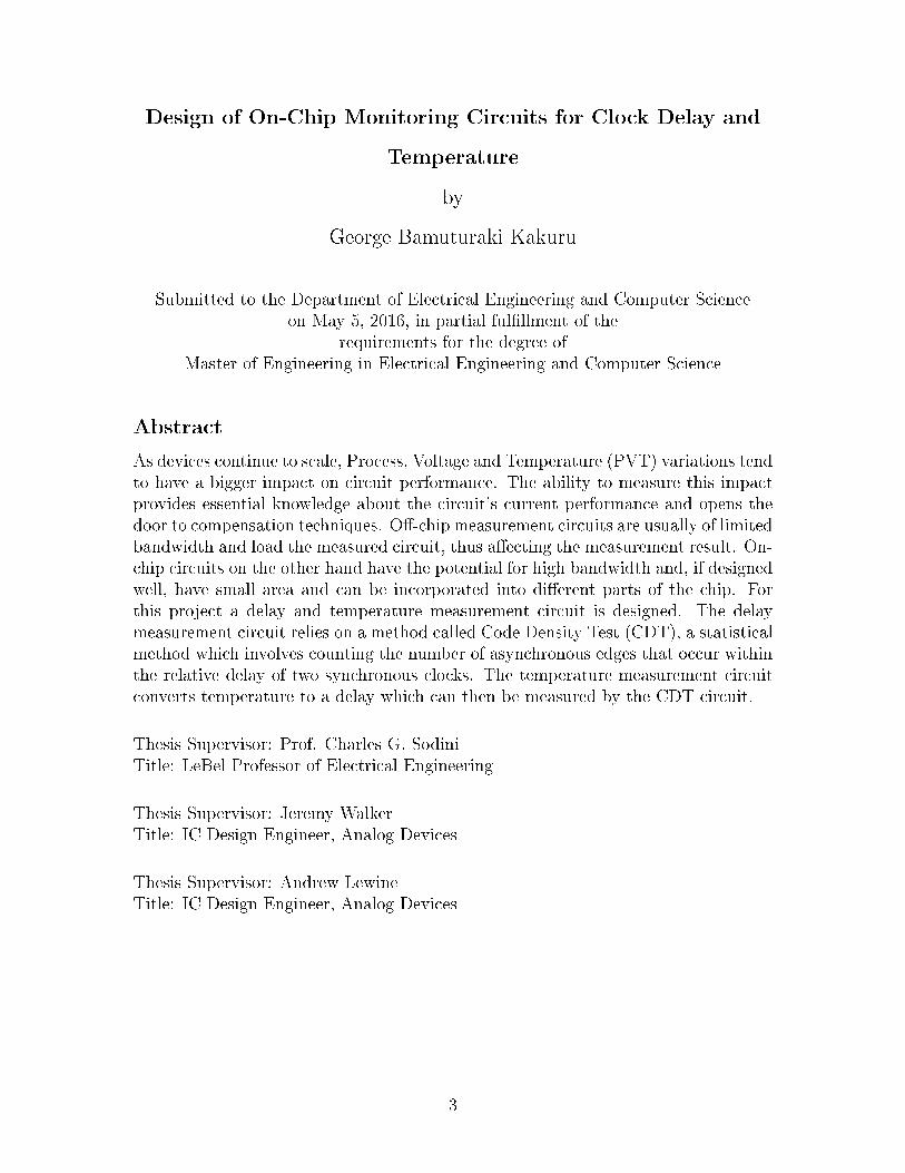
Abstract
As devices continue to scale, Process, Voltage and Temperature (PVT) variations tendto have a bigger impact on circuit performance. The ability to measure this impactprovides essential knowledge about the circuit’s current performance and opens thedoor to compensation techniques. Off-chip measurement circuits are usually of limitedbandwidth and load the measured circuit, thus affecting the measurement result. On-chip circuits on the other hand have the potential for high bandwidth and, if designedwell, have small area and can be incorporated into different parts of the chip. Forthis project a delay and temperature measurement circuit is designed. The delaymeasurement circuit relies on a method called Code Density Test (CDT), a statisticalmethod which involves counting the number of asynchronous edges that occur withinthe relative delay of two synchronous clocks. The temperature measurement circuitconverts temperature to a delay which can then be measured by the CDT circuit.
Thesis Supervisor: Prof. Charles G. SodiniTitle: LeBel Professor of Electrical Engineering
Thesis Supervisor: Jeremy WalkerTitle: IC Design Engineer, Analog Devices
Thesis Supervisor: Andrew LewineTitle: IC Design Engineer, Analog Devices
3

4

Acknowledgments
I would like to thank my supervisors Andrew Lewine and Jeremy Walker. This
thesis would not be anywhere without your help. Even though you were working
on other projects that had strict time commitments, you still ensured that we had
our weekly meeting and were willing to answer my questions whenever I asked. I
thank Pablo Acosta for his suggestion on designing the temperature measurement
circuit. Professor Sodini your guidance cannot go without notice. Thanks for being
my advisor for 6-A.
Andy Wang, Hassan, Terry, Jonathan, and Ben thanks for the lunch and the great
discussions we had over lunch. It was both informative and entertaining. Thanks for
the life lessons too!
I would like to thank Analog Devices Inc. especially the SerDes team for having
given me this opportunity to do my 6-A at such a great company. It was a challenging
journey. I learned a lot about engineering through this project.
I thank my twin brother Gerard Kato for his encouragement and advice when I
most needed it. I thank my parents for having taking me through all my years in
schools. I thank my aunties especially Auntie Tititi and Auntie Bella thanks for all
the guidance and help you have given me ever since I was a kid.
Most especially I would like to thank God for seeing me through all the difficult
times and enabling me to go this far in life.
5

6
Contents
1 Introduction 15
2 Previous Work 17
2.1 Temperature measurement circuits . . . . . . . . . . . . . . . . . . . 17
2.2 Delay measurement circuit . . . . . . . . . . . . . . . . . . . . . . . . 21
2.3 Supply voltage measurement . . . . . . . . . . . . . . . . . . . . . . . 23
2.4 𝑉𝑡ℎ measurement . . . . . . . . . . . . . . . . . . . . . . . . . . . . . 27
3 Temperature and Delay Measurement System 29
3.1 Specifications for the system . . . . . . . . . . . . . . . . . . . . . . . 29
3.2 Clocking . . . . . . . . . . . . . . . . . . . . . . . . . . . . . . . . . . 30
4 Delay Measurement Circuit 33
4.1 Code Density Test (CDT) Theory . . . . . . . . . . . . . . . . . . . . 33
4.1.1 Sampling below Nyquist . . . . . . . . . . . . . . . . . . . . . 36
4.1.2 Setup and Hold time requirements . . . . . . . . . . . . . . . 37
4.2 Code Density Test (CDT) circuit . . . . . . . . . . . . . . . . . . . . 38
4.2.1 Synchronizer . . . . . . . . . . . . . . . . . . . . . . . . . . . . 38
4.2.2 Consecutive hits . . . . . . . . . . . . . . . . . . . . . . . . . . 39
4.2.3 Layout for the delay measurement circuit . . . . . . . . . . . . 39
5 PTAT Current Generation 43
5.1 PTAT circuit resistor choice . . . . . . . . . . . . . . . . . . . . . . . 49
5.2 Layout for PTAT current generator circuit . . . . . . . . . . . . . . . 50
7
6 Dual Slope Circuit 53
6.1 Operation of the Dual Slope circuit . . . . . . . . . . . . . . . . . . . 53
6.2 𝑉𝑟𝑒𝑓 Generation . . . . . . . . . . . . . . . . . . . . . . . . . . . . . . 57
6.3 Selection of switches . . . . . . . . . . . . . . . . . . . . . . . . . . . 58
6.4 Comparator . . . . . . . . . . . . . . . . . . . . . . . . . . . . . . . . 59
6.4.1 Comparator Design . . . . . . . . . . . . . . . . . . . . . . . . 59
6.4.2 Layout floorplan for comparator . . . . . . . . . . . . . . . . . 63
7 Results and Calibration 65
7.1 Power consumption and area of the delay and temperature measure-
ment systems . . . . . . . . . . . . . . . . . . . . . . . . . . . . . . . 65
8 Future work and conclusion 69
A Appendix 71
A.1 Circuit schematics . . . . . . . . . . . . . . . . . . . . . . . . . . . . 71
A.2 Code used . . . . . . . . . . . . . . . . . . . . . . . . . . . . . . . . . 73
8
List of Figures
2-1 Temperature sensor architecture[3] . . . . . . . . . . . . . . . . . . . 18
2-2 Delay line based temperature sensor. The temperature is proportional
to the width of the generated pulse [3]. . . . . . . . . . . . . . . . . . 18
2-3 Delay Cell used in [3] . . . . . . . . . . . . . . . . . . . . . . . . . . . 19
2-4 Delay line based temperature sensor implementation[4] . . . . . . . . 19
2-5 Temperature sensor used in [7] . . . . . . . . . . . . . . . . . . . . . . 20
2-6 Proposed temperature measurement block diagram[6] . . . . . . . . . 21
2-7 Temperature sensor proposed in [9] . . . . . . . . . . . . . . . . . . . 22
2-8 Block diagram for the delay measurement circuit. . . . . . . . . . . . 23
2-9 Dynamic Variation Monitor(DVM) circuit used in [12] . . . . . . . . . 24
2-10 (a) shows the variation in microprocessor 𝐹𝑀𝐴𝑋 , and VCC Droop. (b)
shows the variation in DVM frequency[12]. . . . . . . . . . . . . . . . 24
2-11 Equivalent time measurement . . . . . . . . . . . . . . . . . . . . . . 25
2-12 VCO based ADC operation . . . . . . . . . . . . . . . . . . . . . . . 26
2-13 Voltage supply noise measurement using VCO based ADC[11] . . . . 26
2-14 VCO based supply voltage measurement circuit without sample and
hold circuit[17] . . . . . . . . . . . . . . . . . . . . . . . . . . . . . . 26
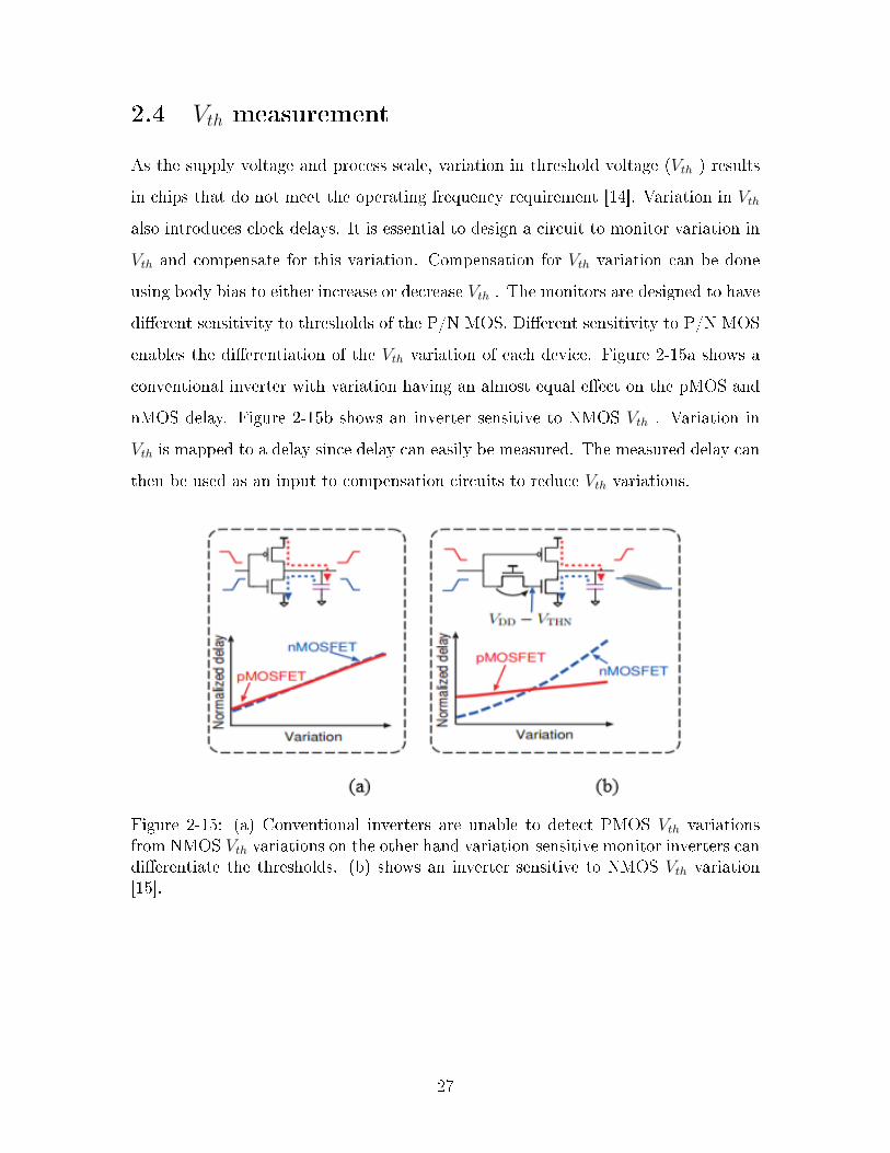
2-15 (a) Conventional inverters are unable to detect PMOS 𝑉𝑡ℎ variations
from NMOS 𝑉𝑡ℎ variations on the other hand variation-sensitive mon-
itor inverters can differentiate the thresholds. (b) shows an inverter
sensitive to NMOS 𝑉𝑡ℎ variation [15]. . . . . . . . . . . . . . . . . . . 27
9
3-1 The temperature measurement circuit showing the conversion from
temperature to a delay and the measurement of the delay using the
CDT circuit. The CDT circuit can be used to measure delay between
two clocks if the two inputs from the temperature conversion to delay
block are replaced with clocks whose relative delay is to be measured. 30
3-2 The variation of ring oscillator frequency with process, supply and tem-
perature. For each temperature (x-axis), the ring oscillator frequency
is plotted for 3 supply voltages (0.8V, 0.9V, 1.05V), and 5 process
corners (ff, fs, sf, ss, tt) . . . . . . . . . . . . . . . . . . . . . . . . . . 32
4-1 A reference clock, and a delayed clock are shown. Both clocks have the
same period, T, but the delayed clock has a delay of d, with respect to
the reference clock. . . . . . . . . . . . . . . . . . . . . . . . . . . . . 34
4-2 The PDF for the distribution of asynchronous clock edges within a
single clock period. . . . . . . . . . . . . . . . . . . . . . . . . . . . . 34
4-3 Fractional error in delay vs the number of asynchronous clocks for
different delay values. . . . . . . . . . . . . . . . . . . . . . . . . . . 35
4-4 a) The error of the delay measurement circuit versus runtime for 1GHz
clocks both for the real and behavioral model delay measurement cir-
cuit implementations. The real delay measurement circuit has setup/hold
time violation around 900ns and thus makes errors. The error repeats
at 1.9ns and 2.9ns. b) Zooming into the error for the behavioral delay
measurement circuit between 2𝜇𝑠 and 20𝜇𝑠 . . . . . . . . . . . . . . . 36
4-5 Sampling an asynchronous clock whose period is less than the delay
between the reference and delayed clocks . . . . . . . . . . . . . . . . 37
4-6 shows setup time violation, 𝑜𝑢𝑡𝑥 is sampling 𝑐𝑙𝑘𝑎𝑠𝑦𝑛. At 823.6𝑛𝑠 𝑜𝑢𝑡𝑥
samples 𝑐𝑙𝑘𝑎𝑠𝑦𝑛 very close to its rising edge and thus the setup time is
less than required. The behavioral model CDT registers this sample
as a hit while the device model misses this hit. . . . . . . . . . . . . . 37
10
4-7 The CDT block diagram showing two sampling flip flops followed by a
synchronizer and retiming circuit, XOR and two counters. . . . . . . 38
4-8 The synchronizer used in the delay measurement circuit. . . . . . . . 39
4-9 Plot showing the CDT transient for a 1GHz reference and delayed
clocks and .5GHz asynchronous clock. . . . . . . . . . . . . . . . . . . 40
4-10 Plot showing the CDT transient for a 1GHz reference and delayed
clocks and .5GHz asynchronous clock. . . . . . . . . . . . . . . . . . . 41
5-1 PTAT current generation circuit a) with high supply sensitivity and b)
with low supply sensitivity. . . . . . . . . . . . . . . . . . . . . . . . . 44
5-2 The bias circuitry for the PTAT current generator. The vcascp bias
generator current source is not cascoded due to the low value of voltage
and hence low headroom for the current source MN1. . . . . . . . . . 45
5-3 Plots of the supply sensitivity before and after cascoding. The non cas-
code circuit has a variation of 8.5𝜇𝐴 while the cascode has a variation
of 1𝜇𝐴. . . . . . . . . . . . . . . . . . . . . . . . . . . . . . . . . . . . 46
5-4 Plots for the headroom of the devices in the PTAT current generator
circuit and the bias generator . . . . . . . . . . . . . . . . . . . . . . 47
5-5 Plots for the headroom of the devices in the PTAT current generator
circuit and the bias generator . . . . . . . . . . . . . . . . . . . . . . 47
5-6 Plots for the headroom of the devices in the PTAT current generator
circuit and the bias generator . . . . . . . . . . . . . . . . . . . . . . 48
5-7 PTAT startup circuit. . . . . . . . . . . . . . . . . . . . . . . . . . . . 49
5-8 Transient simulations showing the startup circuit node voltages X and
Y. Simulations were done for process corners ss,sf,fs,ff and tt, supply
voltages 0.8V,.9V, and 1.05V at −40∘𝐶. . . . . . . . . . . . . . . . . 49
5-9 A plot of generated current versus temperature for different resistors . 50
5-10 Layout for the PTAT current generator circuit. It occupies an area of
68𝜇𝑚 by 32𝜇𝑚. . . . . . . . . . . . . . . . . . . . . . . . . . . . . . . 51
11
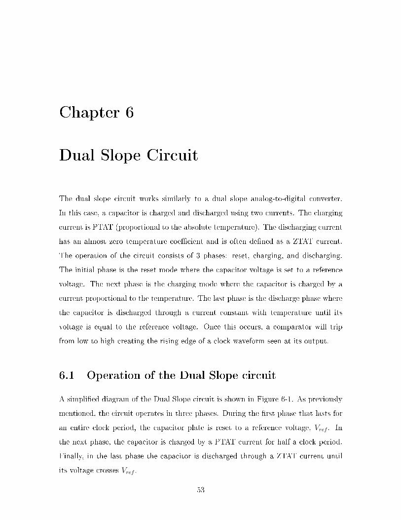
6-1 a) Dual slope circuit and b) The different clock phases of the Dual
slope circuit . . . . . . . . . . . . . . . . . . . . . . . . . . . . . . . . 54
6-2 A plot of capacitor voltage variation over time for two different tem-
perature showing how the delay varies with the charging current hence
temperature. . . . . . . . . . . . . . . . . . . . . . . . . . . . . . . . . 54
6-3 The schematic for the dual slope circuit without the comparator . . . 56
6-4 Transient simulation for the Dual slope circuit showing voltage across
the 𝑣𝑥 switch. It takes time before the switch drop is low enough. . . 57
6-5 A differential amplifier with resistor loads. . . . . . . . . . . . . . . . 60
6-6 The full comparator excluding the output of the inverter stages. . . . 60
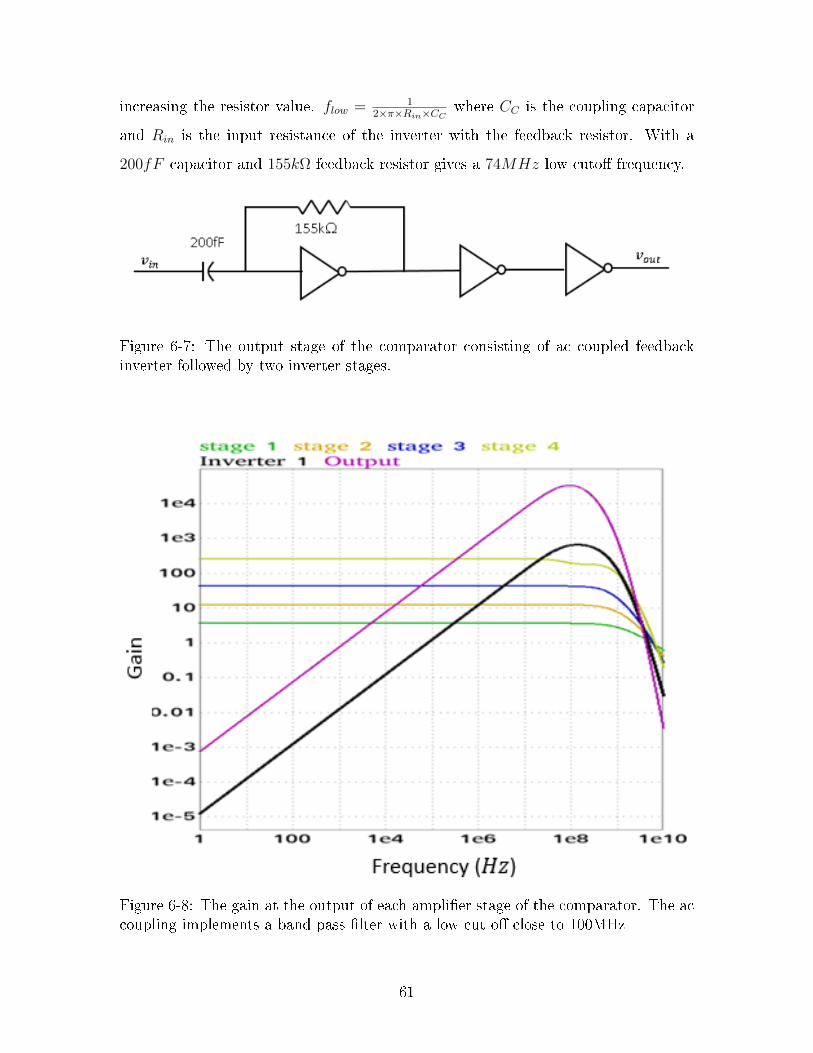
6-7 The output stage of the comparator consisting of ac coupled feedback
inverter followed by two inverter stages. . . . . . . . . . . . . . . . . . 61
6-8 The gain at the output of each amplifier stage of the comparator. The
ac coupling implements a band pass filter with a low cut off close to
100MHz . . . . . . . . . . . . . . . . . . . . . . . . . . . . . . . . . . 61
6-9 a) A transient simulation for the comparator showing the delay through
the comparator for a 10mV input differential signal b) The gain at the
output of the differential to single ended amplifier. . . . . . . . . . . . 62
6-10 The delay added by comparator 1 and 2 to the reference and delayed
clocks respectively, and the difference in the two added delays. . . . . 63
6-11 The schematic for the two comparators used to produce the two clocks
whose relative delay is proportional to the temperature. . . . . . . . . 64
6-12 Layout floorplan for the comparator. . . . . . . . . . . . . . . . . . . 64
7-1 A plot of delay versus temperature for all 15 cases using two comparators. 67
7-2 Plots of the error versus temperature. a shows the error with an ideal
comparator while b shows the error using the real comparator. The
error ranges from −2.2∘𝐶 to 7.6∘C for the real comparator. . . . . . . 68
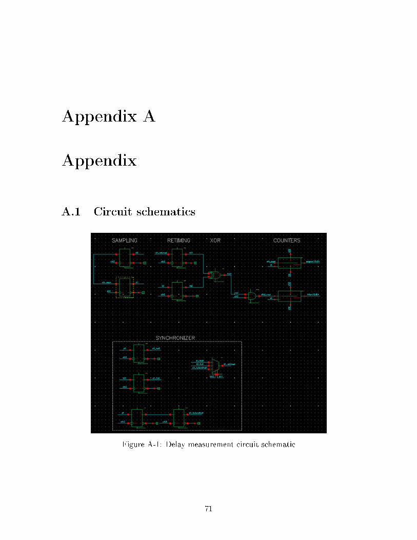
A-1 Delay measurement circuit schematic . . . . . . . . . . . . . . . . . . 71
A-2 PTAT current generator circuit . . . . . . . . . . . . . . . . . . . . . 72
12
A-3 PTAT Bias generator circuit . . . . . . . . . . . . . . . . . . . . . . . 73
A-4 Comparator circuit . . . . . . . . . . . . . . . . . . . . . . . . . . . . 74
13

14
Chapter 1
Introduction
Circuit verification and diagnosis are essential for failure detection, good performance,
and yield of a circuit. Diagnosis can either be done on chip or off chip. Off chip
measurements involve the use of expensive test equipment. The equipment also lacks
repeatability and often results in long test times [1]. Off chip circuits also load the
circuit under test (CUT). Probes used to connect the CUT to the test equipment
usually have a low bandwidth which leads to a filtered signal. The probes may also
have a relative delay which varies with temperature and will affect the accuracy of the
measured result. This calls for on-chip measurement circuits. On-chip measurement
circuits can do most of the required measurements, e.g. voltage, temperature, and
delay, on the chip and output a digital code to be measured off-chip.
In this thesis I present an on-chip circuit to measure temperature and delay. The
temperature measurement circuit relies on the delay measurement circuit. The delay
measurement circuit uses Code Density Test (CDT), a statistical method to measure
the delay between two clocks [10]. The rest of the thesis is organized into the different
sections as shown below:
∙ Chapter 2 presents previous on-chip measurement circuits.
∙ Chapter 3 presents the temperature measurement circuit.
15
∙ Chapter 4 presents the delay measurement circuit.
∙ Chapter 5 presents the generation of Proportional to the absolute temperature
(PTAT) current.
∙ Chapter 6 presents the Dual Slope converter used to convert the PTAT current
into a delay.
∙ Chapter 7 presents the results and possible calibration for the temperature
measurement circuit.
∙ Chapter 8 summarizes possible future work and concludes the thesis.
16
Chapter 2
Previous Work
2.1 Temperature measurement circuits
Temperature variation affects the performance of circuits and if not accounted for
could lead to poor performance of circuits under certain conditions. Several temper-
ature measurement circuits have been proposed. BJT based temperature sensors are
usually accurate and easier to design but they require high voltage headroom and also
occupy larger area than CMOS based sensors. A BJT based temperature sensor with
high resolution but large area and high supply voltage requirement is presented in [2].
CMOS-based temperature sensors are presented in [3, 4, 5, 6, 7]. It’s well-known that
the transconductance of transistors tends to decrease with temperature. Monitoring
the temperature may allow the addition of circuitry to compensate for this.
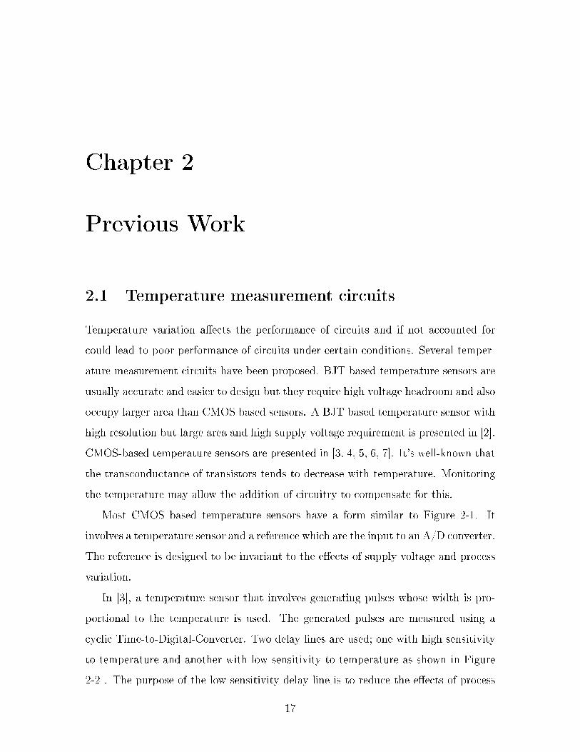
Most CMOS based temperature sensors have a form similar to Figure 2-1. It
involves a temperature sensor and a reference which are the input to an A/D converter.
The reference is designed to be invariant to the effects of supply voltage and process
variation.
In [3], a temperature sensor that involves generating pulses whose width is pro-
portional to the temperature is used. The generated pulses are measured using a
cyclic Time-to-Digital-Converter. Two delay lines are used; one with high sensitivity
to temperature and another with low sensitivity to temperature as shown in Figure
2-2 . The purpose of the low sensitivity delay line is to reduce the effects of process
17
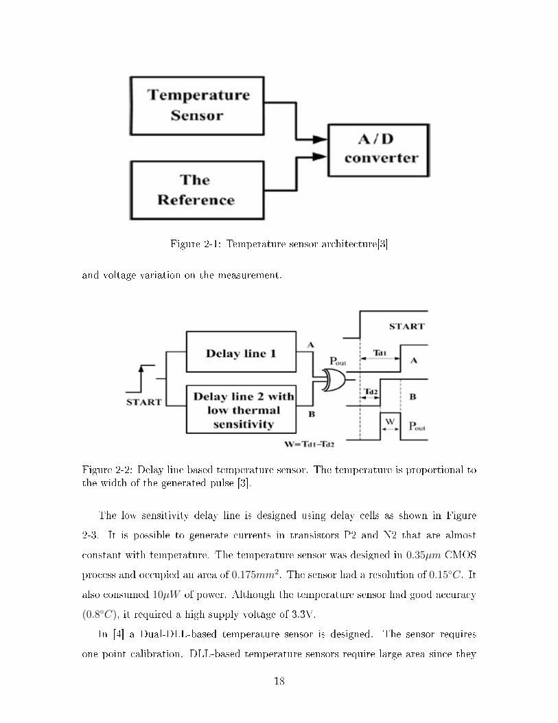
Figure 2-1: Temperature sensor architecture[3]
and voltage variation on the measurement.
Figure 2-2: Delay line based temperature sensor. The temperature is proportional tothe width of the generated pulse [3].
The low sensitivity delay line is designed using delay cells as shown in Figure
2-3. It is possible to generate currents in transistors P2 and N2 that are almost
constant with temperature. The temperature sensor was designed in 0.35𝜇𝑚 CMOS
process and occupied an area of 0.175𝑚𝑚2. The sensor had a resolution of 0.15∘𝐶. It
also consumed 10𝜇𝑊 of power. Although the temperature sensor had good accuracy
(0.8∘𝐶), it required a high supply voltage of 3.3V.
In [4] a Dual-DLL-based temperature sensor is designed. The sensor requires
one point calibration. DLL-based temperature sensors require large area since they
18
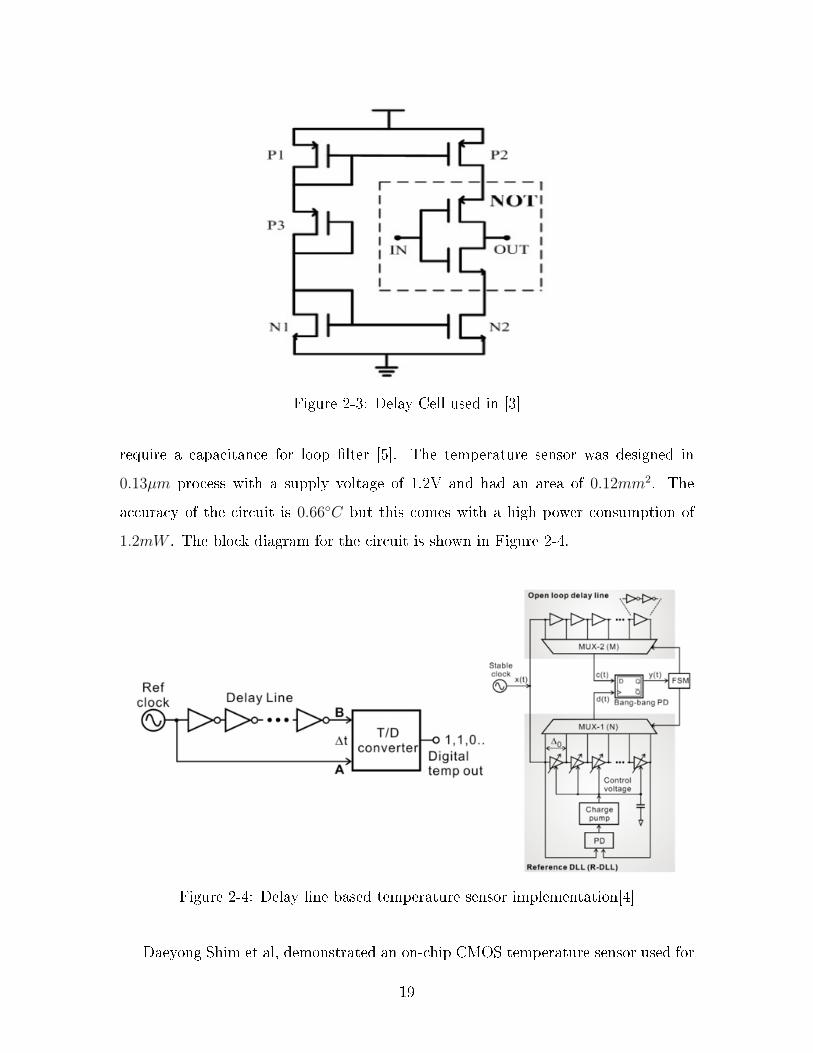
Figure 2-3: Delay Cell used in [3]
require a capacitance for loop filter [5]. The temperature sensor was designed in
0.13𝜇𝑚 process with a supply voltage of 1.2V and had an area of 0.12𝑚𝑚2. The
accuracy of the circuit is 0.66∘𝐶 but this comes with a high power consumption of
1.2𝑚𝑊 . The block diagram for the circuit is shown in Figure 2-4.
Figure 2-4: Delay line based temperature sensor implementation[4]
Daeyong Shim et al, demonstrated an on-chip CMOS temperature sensor used for
19

self-refresh of low power mobile DRAM. The basic temperature sensor is shown in Fig-
ure 2-5 . MOSFET M1 operates in triode region while M2 operates in saturation. The
voltage 𝑉𝑁𝑂𝐷𝐸 is a linear function of temperature since the resistance of M1 increases
with temperature. On the other hand the voltage 𝑉𝑂𝑈𝑇 decreases with temperature
since M2 acts as a degenerated common source amplifier to the 𝑉𝑁𝑂𝐷𝐸 signal. The
derivation for the equations of the two voltages is done in [7]. 𝑉𝑂𝑈𝑇 is compared
against five reference voltages generated by a resistor ladder.The temperature sensor
has a sensitivity of −3.2𝑚𝑉/∘𝐶 and achieved a resolution of 1.94∘𝐶. It also required
1 point calibration, occupied a small area of 0.001725𝑚𝑚2 and dissipated 0.33𝜇𝑊 of
power.
Figure 2-5: Temperature sensor used in [7]
Poki Chen et al demonstrated a timing comparator based temperature sensor
shown in Figure 2-6. The architecture is similar to [3] with an additional MUX and
dummy MUX. The MUX is used to select the delay from a reference delay line. The
two delays are then compared using a timing comparator. The power dissipated is
9𝜇𝑊 . The sensor occupies an error of 0.3969𝑚𝑚2. It also has an error of less than
0.8∘𝐶 over the range −40∘𝐶 to 95∘𝐶 [6].
In [5], a ring oscillator and Frequency-to-Digital Converter (FDC) is used to pro-
duce a very high-resolution temperature measurement circuit. The resolution of the
circuit is 0.34∘𝐶. The circuit occupies an area of 0.0013𝑚𝑚2 with a power consump-
20
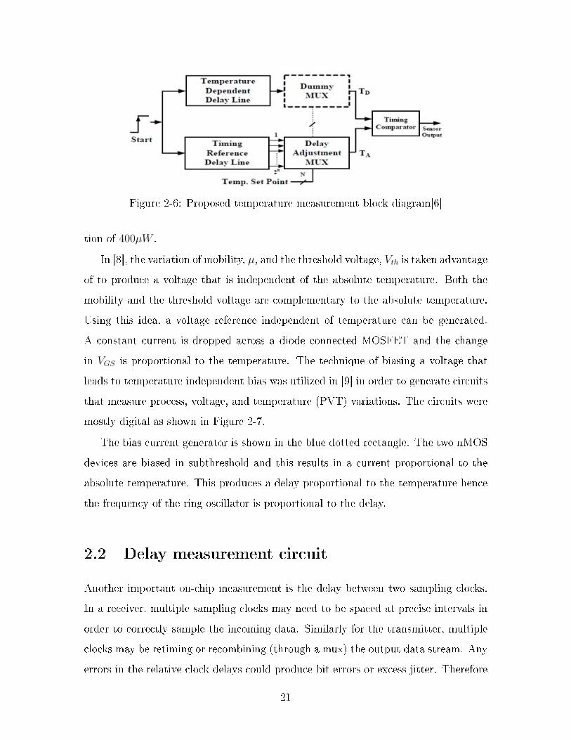
Figure 2-6: Proposed temperature measurement block diagram[6]
tion of 400𝜇𝑊 .
In [8], the variation of mobility, 𝜇, and the threshold voltage, 𝑉𝑡ℎ is taken advantage
of to produce a voltage that is independent of the absolute temperature. Both the
mobility and the threshold voltage are complementary to the absolute temperature.
Using this idea, a voltage reference independent of temperature can be generated.
A constant current is dropped across a diode connected MOSFET and the change
in 𝑉𝐺𝑆 is proportional to the temperature. The technique of biasing a voltage that
leads to temperature independent bias was utilized in [9] in order to generate circuits
that measure process, voltage, and temperature (PVT) variations. The circuits were
mostly digital as shown in Figure 2-7.
The bias current generator is shown in the blue dotted rectangle. The two nMOS
devices are biased in subthreshold and this results in a current proportional to the
absolute temperature. This produces a delay proportional to the temperature hence
the frequency of the ring oscillator is proportional to the delay.
2.2 Delay measurement circuit
Another important on-chip measurement is the delay between two sampling clocks.
In a receiver, multiple sampling clocks may need to be spaced at precise intervals in
order to correctly sample the incoming data. Similarly for the transmitter, multiple
clocks may be retiming or recombining (through a mux) the output data stream. Any
errors in the relative clock delays could produce bit errors or excess jitter. Therefore
21
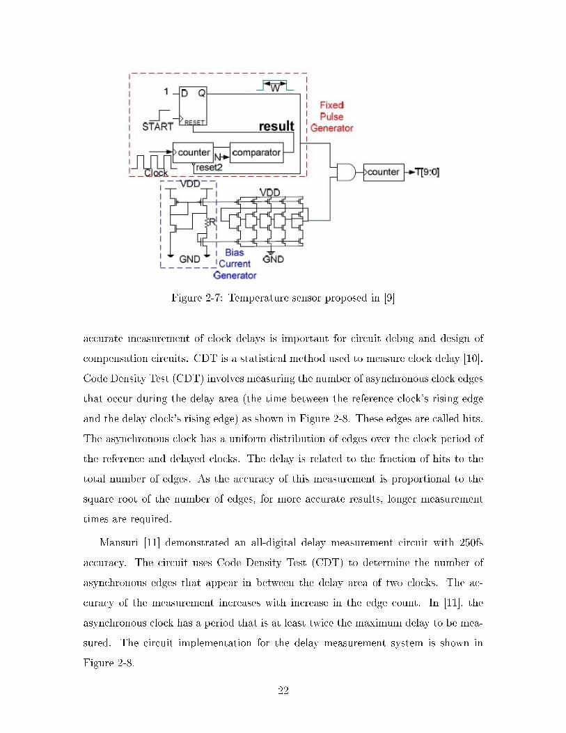
Figure 2-7: Temperature sensor proposed in [9]
accurate measurement of clock delays is important for circuit debug and design of
compensation circuits. CDT is a statistical method used to measure clock delay [10].
Code Density Test (CDT) involves measuring the number of asynchronous clock edges
that occur during the delay area (the time between the reference clock’s rising edge
and the delay clock’s rising edge) as shown in Figure 2-8. These edges are called hits.
The asynchronous clock has a uniform distribution of edges over the clock period of
the reference and delayed clocks. The delay is related to the fraction of hits to the
total number of edges. As the accuracy of this measurement is proportional to the
square root of the number of edges, for more accurate results, longer measurement
times are required.
Mansuri [11] demonstrated an all-digital delay measurement circuit with 250fs
accuracy. The circuit uses Code Density Test (CDT) to determine the number of
asynchronous edges that appear in between the delay area of two clocks. The ac-
curacy of the measurement increases with increase in the edge count. In [11], the
asynchronous clock has a period that is at least twice the maximum delay to be mea-
sured. The circuit implementation for the delay measurement system is shown in
Figure 2-8.
22
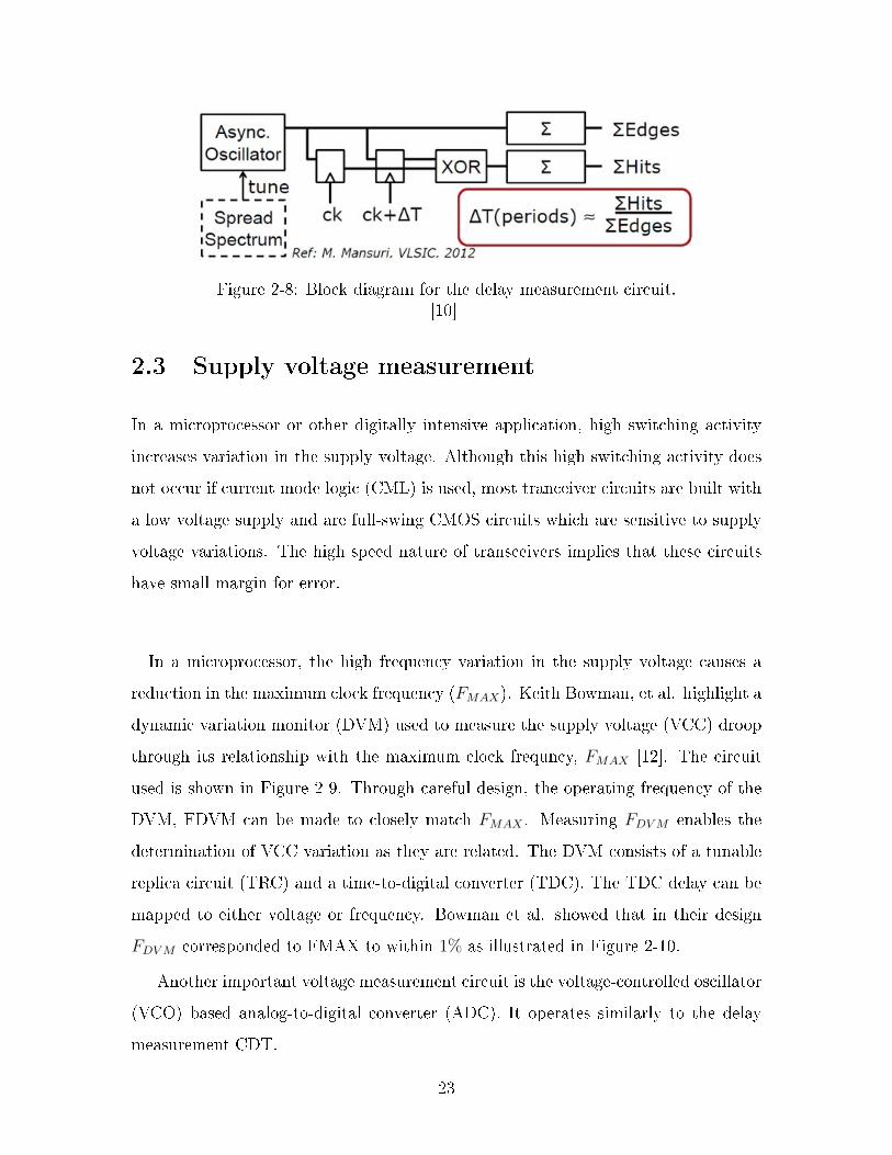
Figure 2-8: Block diagram for the delay measurement circuit.[10]
2.3 Supply voltage measurement
In a microprocessor or other digitally intensive application, high switching activity
increases variation in the supply voltage. Although this high switching activity does
not occur if current mode logic (CML) is used, most tranceiver circuits are built with
a low voltage supply and are full-swing CMOS circuits which are sensitive to supply
voltage variations. The high speed nature of transceivers implies that these circuits
have small margin for error.
In a microprocessor, the high frequency variation in the supply voltage causes a
reduction in the maximum clock frequency (𝐹𝑀𝐴𝑋). Keith Bowman, et al. highlight a
dynamic variation monitor (DVM) used to measure the supply voltage (VCC) droop
through its relationship with the maximum clock frequncy, 𝐹𝑀𝐴𝑋 [12]. The circuit
used is shown in Figure 2-9. Through careful design, the operating frequency of the
DVM, FDVM can be made to closely match 𝐹𝑀𝐴𝑋 . Measuring 𝐹𝐷𝑉𝑀 enables the
determination of VCC variation as they are related. The DVM consists of a tunable
replica circuit (TRC) and a time-to-digital converter (TDC). The TDC delay can be
mapped to either voltage or frequency. Bowman et al. showed that in their design
𝐹𝐷𝑉𝑀 corresponded to FMAX to within 1% as illustrated in Figure 2-10.
Another important voltage measurement circuit is the voltage-controlled oscillator
(VCO) based analog-to-digital converter (ADC). It operates similarly to the delay
measurement CDT.
23

Figure 2-9: Dynamic Variation Monitor(DVM) circuit used in [12]
Figure 2-10: (a) shows the variation in microprocessor 𝐹𝑀𝐴𝑋 , and VCC Droop. (b)shows the variation in DVM frequency[12].
If supply noise is periodic with a single frequency, use of equivalent-time sampling
shown in Figure 2-11 reduces the sampling rate requirement. Equivalent-time mea-
surement involves sampling a periodic signal several times and getting the average
value of the samples. Equivalent-time measurement also has the advantage of aver-
aging out the random supply noise since its average value is 0.
By sampling the supply voltage at two different times, it is possible to compute the
autocorrelation. The autocorrelation is related to how much variation a signal has.
Slowly varying signals have a flatter autocorrelation while rapidly varying signals have
a steeper autocorrelation. The power spectral density (PSD) is acquired by taking
the Fourier transform of the autocorrelation. Knowing the power spectral density can
24
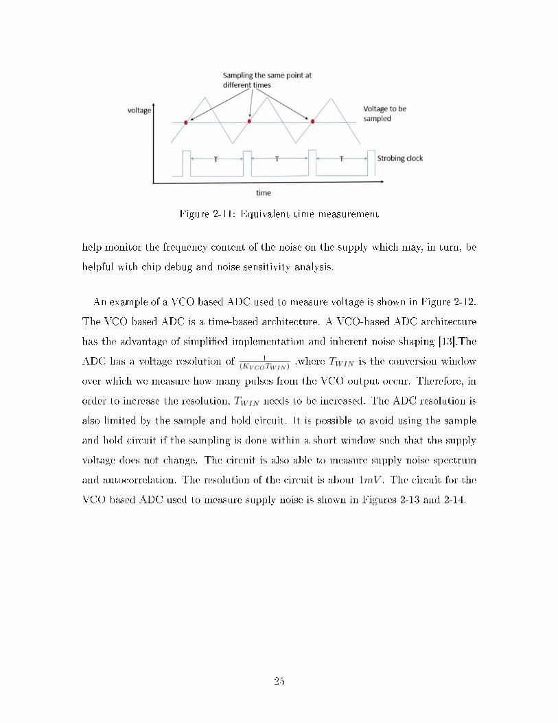
Figure 2-11: Equivalent time measurement
help monitor the frequency content of the noise on the supply which may, in turn, be
helpful with chip debug and noise sensitivity analysis.
An example of a VCO based ADC used to measure voltage is shown in Figure 2-12.
The VCO based ADC is a time-based architecture. A VCO-based ADC architecture
has the advantage of simplified implementation and inherent noise shaping [13].The
ADC has a voltage resolution of 1(𝐾𝑉 𝐶𝑂𝑇𝑊𝐼𝑁 )
,where 𝑇𝑊𝐼𝑁 is the conversion window
over which we measure how many pulses from the VCO output occur. Therefore, in
order to increase the resolution, 𝑇𝑊𝐼𝑁 needs to be increased. The ADC resolution is
also limited by the sample and hold circuit. It is possible to avoid using the sample
and hold circuit if the sampling is done within a short window such that the supply
voltage does not change. The circuit is also able to measure supply noise spectrum
and autocorrelation. The resolution of the circuit is about 1𝑚𝑉 . The circuit for the
VCO based ADC used to measure supply noise is shown in Figures 2-13 and 2-14.
25
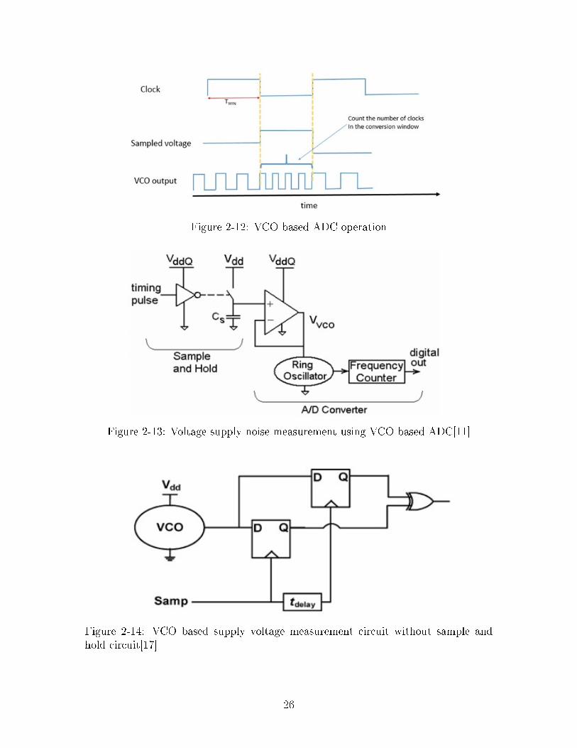
Figure 2-12: VCO based ADC operation
Figure 2-13: Voltage supply noise measurement using VCO based ADC[11]
Figure 2-14: VCO based supply voltage measurement circuit without sample andhold circuit[17]
26
2.4 𝑉𝑡ℎ measurement
As the supply voltage and process scale, variation in threshold voltage (𝑉𝑡ℎ ) results
in chips that do not meet the operating frequency requirement [14]. Variation in 𝑉𝑡ℎ
also introduces clock delays. It is essential to design a circuit to monitor variation in
𝑉𝑡ℎ and compensate for this variation. Compensation for 𝑉𝑡ℎ variation can be done
using body bias to either increase or decrease 𝑉𝑡ℎ . The monitors are designed to have
different sensitivity to thresholds of the P/N MOS. Different sensitivity to P/N MOS
enables the differentiation of the 𝑉𝑡ℎ variation of each device. Figure 2-15a shows a
conventional inverter with variation having an almost equal effect on the pMOS and
nMOS delay. Figure 2-15b shows an inverter sensitive to NMOS 𝑉𝑡ℎ . Variation in
𝑉𝑡ℎ is mapped to a delay since delay can easily be measured. The measured delay can
then be used as an input to compensation circuits to reduce 𝑉𝑡ℎ variations.
Figure 2-15: (a) Conventional inverters are unable to detect PMOS 𝑉𝑡ℎ variationsfrom NMOS 𝑉𝑡ℎ variations on the other hand variation-sensitive monitor inverters candifferentiate the thresholds. (b) shows an inverter sensitive to NMOS 𝑉𝑡ℎ variation[15].
27

28
Chapter 3
Temperature and Delay Measurement
System
The temperature measurement system consists of a current generator circuit, dual
slope converter, and the delay measurement circuit as shown in Figure 3-1. First
using a reference clock, a delayed clock is generated using the PTAT current generator
and the dual slope circuit. The delay between the reference clock and the delayed
clock is proportional to the temperature. The delayed and reference clocks are the
inputs for the delay measurement circuit. An asynchronous clock is generated using
a ring oscillator or can be supplied externally. The temperature is proportional to
the digital output code from the delay measurement circuit.
3.1 Specifications for the system
The initial specifications for the system were set at power of less than 10mW, area less
than 100𝜇𝑚 × 100𝜇𝑚, and an accuracy of ±5∘𝐶 over the entire temperature range
(−40∘𝐶 to 125∘𝐶). The circuit specifications are shown in Table 3.1. The temperature
measurement system requires a clock whose frequency is stable over PVT. This can
be acquired from a clock generated by a PLL which is likely to already exist on
the chip. The dual slope circuit requires an input bias current with no variation
over temperature ( referred to as a ZTAT current). The delay measurement system
29
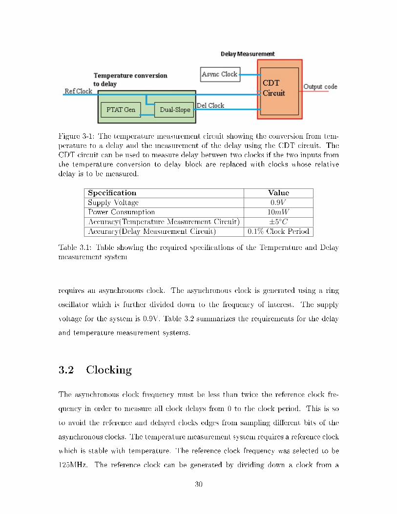
Figure 3-1: The temperature measurement circuit showing the conversion from tem-perature to a delay and the measurement of the delay using the CDT circuit. TheCDT circuit can be used to measure delay between two clocks if the two inputs fromthe temperature conversion to delay block are replaced with clocks whose relativedelay is to be measured.
Specification ValueSupply Voltage 0.9𝑉Power Consumption 10𝑚𝑊Accuracy(Temperature Measurement Circuit) ±5∘𝐶Accuracy(Delay Measurement Circuit) 0.1% Clock Period
Table 3.1: Table showing the required specifications of the Temperature and Delaymeasurement system
requires an asynchronous clock. The asynchronous clock is generated using a ring
oscillator which is further divided down to the frequency of interest. The supply
voltage for the system is 0.9V. Table 3.2 summarizes the requirements for the delay
and temperature measurement systems.
3.2 Clocking
The asynchronous clock frequency must be less than twice the reference clock fre-
quency in order to measure all clock delays from 0 to the clock period. This is so
to avoid the reference and delayed clocks edges from sampling different bits of the
asynchronous clocks. The temperature measurement system requires a reference clock
which is stable with temperature. The reference clock frequency was selected to be
125MHz. The reference clock can be generated by dividing down a clock from a
30
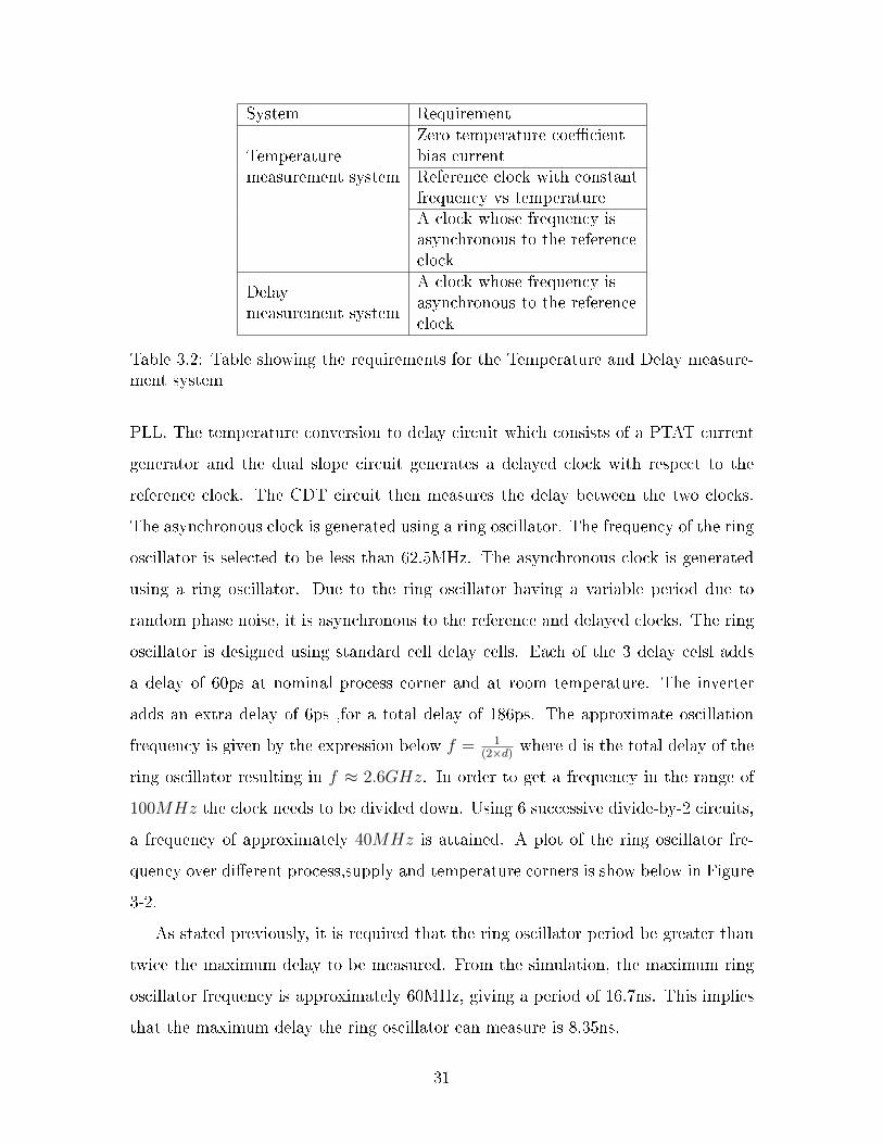
System Requirement
Temperaturemeasurement system
Zero temperature coefficientbias currentReference clock with constantfrequency vs temperatureA clock whose frequency isasynchronous to the referenceclock
Delaymeasurement system
A clock whose frequency isasynchronous to the referenceclock
Table 3.2: Table showing the requirements for the Temperature and Delay measure-ment system
PLL. The temperature conversion to delay circuit which consists of a PTAT current
generator and the dual slope circuit generates a delayed clock with respect to the
reference clock. The CDT circuit then measures the delay between the two clocks.
The asynchronous clock is generated using a ring oscillator. The frequency of the ring
oscillator is selected to be less than 62.5MHz. The asynchronous clock is generated
using a ring oscillator. Due to the ring oscillator having a variable period due to
random phase noise, it is asynchronous to the reference and delayed clocks. The ring
oscillator is designed using standard cell delay cells. Each of the 3 delay celsl adds
a delay of 60ps at nominal process corner and at room temperature. The inverter
adds an extra delay of 6ps ,for a total delay of 186ps. The approximate oscillation
frequency is given by the expression below 𝑓 = 1(2×𝑑)
where d is the total delay of the
ring oscillator resulting in 𝑓 ≈ 2.6𝐺𝐻𝑧. In order to get a frequency in the range of
100𝑀𝐻𝑧 the clock needs to be divided down. Using 6 successive divide-by-2 circuits,
a frequency of approximately 40𝑀𝐻𝑧 is attained. A plot of the ring oscillator fre-
quency over different process,supply and temperature corners is show below in Figure
3-2.
As stated previously, it is required that the ring oscillator period be greater than
twice the maximum delay to be measured. From the simulation, the maximum ring
oscillator frequency is approximately 60MHz, giving a period of 16.7ns. This implies
that the maximum delay the ring oscillator can measure is 8.35ns.
31
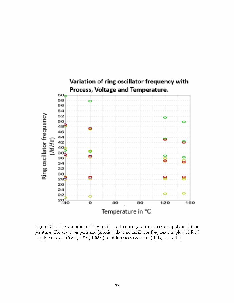
Figure 3-2: The variation of ring oscillator frequency with process, supply and tem-perature. For each temperature (x-axis), the ring oscillator frequency is plotted for 3supply voltages (0.8V, 0.9V, 1.05V), and 5 process corners (ff, fs, sf, ss, tt)
32
Chapter 4
Delay Measurement Circuit
The delay measurement circuit is similar to that presented in [1]. The circuit uses
the Code Density Test (CDT) method to measure delay between two clocks with the
same period using a third clock. This third clock is asynchronous to the first two and
therefore provides a uniform distribution of sampling instants within the period of the
first two clocks. The system counts the number of asynchronous edges that occurs
within the area between the rising edges of the two measured clock. The total delay is
proportional to the ratio of the number of edges that occurs within the area between
the rising edges of the two measured clocks to the total number of edges. The delay
measurement is implemented using only digital circuits, reducing the complexity of
the design, and making it impervious to PVT variation.
4.1 Code Density Test (CDT) Theory
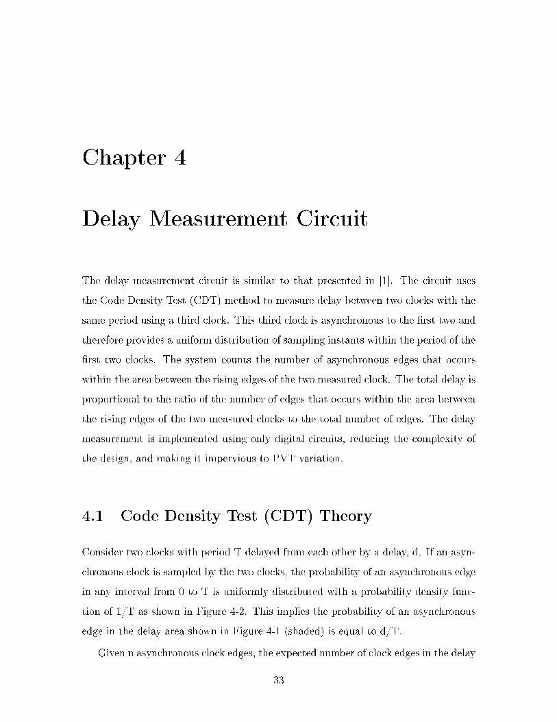
Consider two clocks with period T delayed from each other by a delay, d. If an asyn-
chronous clock is sampled by the two clocks, the probability of an asynchronous edge
in any interval from 0 to T is uniformly distributed with a probability density func-
tion of 1/T as shown in Figure 4-2. This implies the probability of an asynchronous
edge in the delay area shown in Figure 4-1 (shaded) is equal to d/T.
Given n asynchronous clock edges, the expected number of clock edges in the delay
33
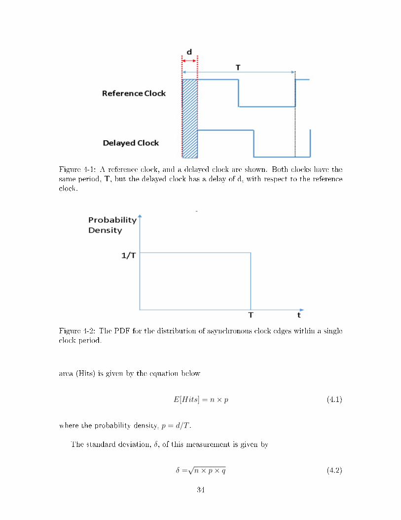
Figure 4-1: A reference clock, and a delayed clock are shown. Both clocks have thesame period, T, but the delayed clock has a delay of d, with respect to the referenceclock.
Figure 4-2: The PDF for the distribution of asynchronous clock edges within a singleclock period.
area (Hits) is given by the equation below
𝐸[𝐻𝑖𝑡𝑠] = 𝑛× 𝑝 (4.1)
where the probability density, 𝑝 = 𝑑/𝑇 .
The standard deviation, 𝛿, of this measurement is given by
𝛿 =√𝑛× 𝑝× 𝑞 (4.2)
34
where 𝑞 = 1 − 𝑝. Using equation 4.1 means the measured delay, 𝑑𝑚 = 𝑇𝑛𝐻𝑖𝑡𝑠. The
error, 𝜖 in 𝑑𝑚 is related to the standard deviation. Therefore
𝜖 ≈ 𝑇
𝑛𝛿 (4.3)
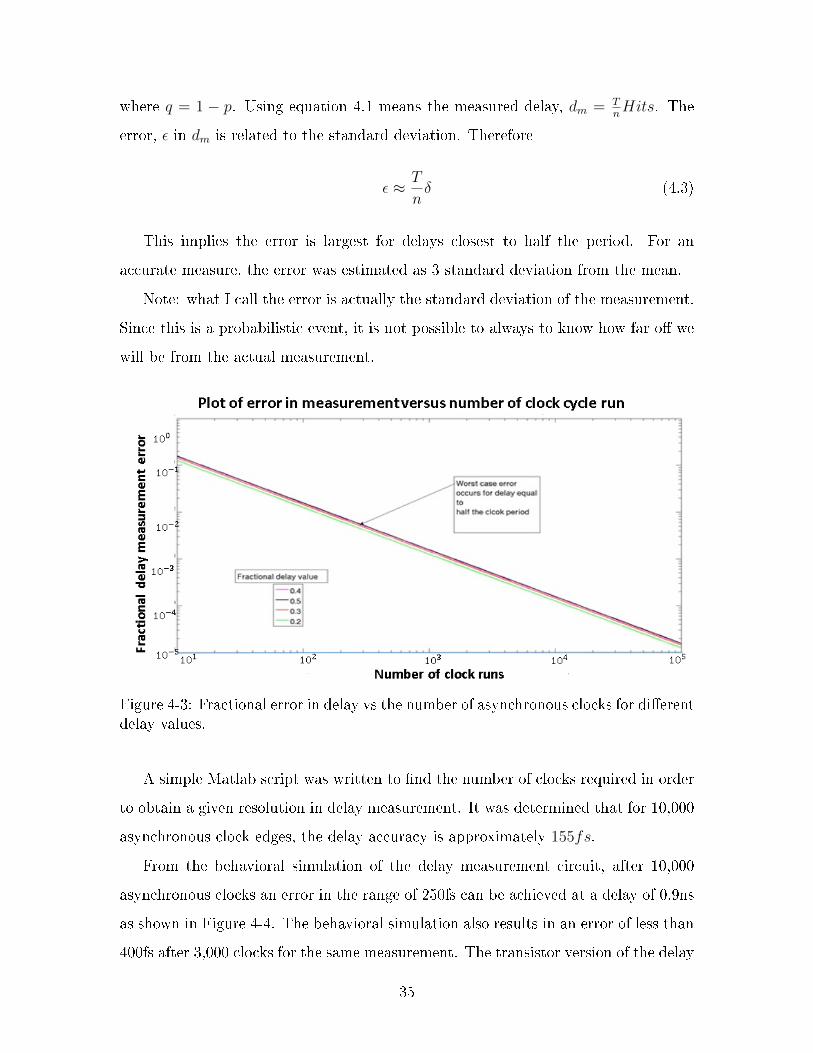
This implies the error is largest for delays closest to half the period. For an
accurate measure, the error was estimated as 3 standard deviation from the mean.
Note: what I call the error is actually the standard deviation of the measurement.
Since this is a probabilistic event, it is not possible to always to know how far off we
will be from the actual measurement.
Figure 4-3: Fractional error in delay vs the number of asynchronous clocks for differentdelay values.
A simple Matlab script was written to find the number of clocks required in order
to obtain a given resolution in delay measurement. It was determined that for 10,000
asynchronous clock edges, the delay accuracy is approximately 155𝑓𝑠.
From the behavioral simulation of the delay measurement circuit, after 10,000
asynchronous clocks an error in the range of 250fs can be achieved at a delay of 0.9ns
as shown in Figure 4-4. The behavioral simulation also results in an error of less than
400fs after 3,000 clocks for the same measurement. The transistor version of the delay
35
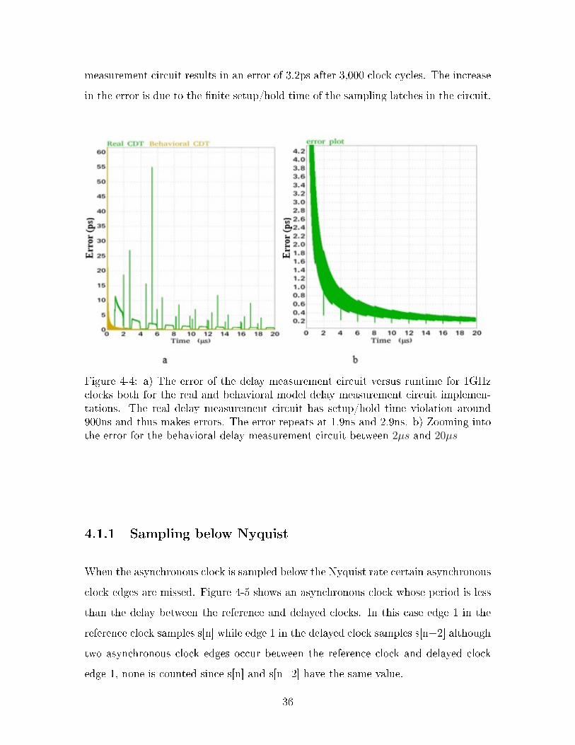
measurement circuit results in an error of 3.2ps after 3,000 clock cycles. The increase
in the error is due to the finite setup/hold time of the sampling latches in the circuit.
Figure 4-4: a) The error of the delay measurement circuit versus runtime for 1GHzclocks both for the real and behavioral model delay measurement circuit implemen-tations. The real delay measurement circuit has setup/hold time violation around900ns and thus makes errors. The error repeats at 1.9ns and 2.9ns. b) Zooming intothe error for the behavioral delay measurement circuit between 2𝜇𝑠 and 20𝜇𝑠
4.1.1 Sampling below Nyquist
When the asynchronous clock is sampled below the Nyquist rate certain asynchronous
clock edges are missed. Figure 4-5 shows an asynchronous clock whose period is less
than the delay between the reference and delayed clocks. In this case edge 1 in the
reference clock samples s[n] while edge 1 in the delayed clock samples s[n+2] although
two asynchronous clock edges occur between the reference clock and delayed clock
edge 1, none is counted since s[n] and s[n+2] have the same value.
36

Figure 4-5: Sampling an asynchronous clock whose period is less than the delaybetween the reference and delayed clocks
4.1.2 Setup and Hold time requirements
It is important to consider the effect of setup and hold time requirements for the CDT
sampling latches. If the asynchronous edge lies within the setup or hold time, the
output from the latch is not properly resolved. In the worst case, all the asynchronous
edges that lie in the setup or hold time are incorrectly resolved. This gives an error
equal to the sum of the setup and hold time. For example consider a clock with a
period of 1𝑛𝑠. If the setup and hold time are both 10𝑝𝑠, for a delay of 400𝑝𝑠, our
circuit would measure 400𝑝𝑠− 𝑡𝑠𝑒𝑡𝑢𝑝 − 𝑡ℎ𝑜𝑙𝑑 = 380𝑝𝑠.
Figure 4-6: shows setup time violation, 𝑜𝑢𝑡𝑥 is sampling 𝑐𝑙𝑘𝑎𝑠𝑦𝑛. At 823.6𝑛𝑠 𝑜𝑢𝑡𝑥samples 𝑐𝑙𝑘𝑎𝑠𝑦𝑛 very close to its rising edge and thus the setup time is less thanrequired. The behavioral model CDT registers this sample as a hit while the devicemodel misses this hit.
37
4.2 Code Density Test (CDT) circuit
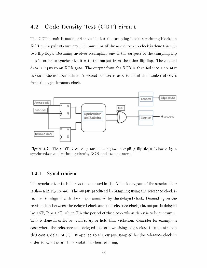
The CDT circuit is made of 4 main blocks: the sampling block, a retiming block, an
XOR and a pair of counters. The sampling of the asynchronous clock is done through
two flip flops. Retiming involves resampling one of the outputs of the sampling flip
flop in order to synchronize it with the output from the other flip flop. The aligned
data is input to an XOR gate. The output from the XOR is then fed into a counter
to count the number of hits. A second counter is used to count the number of edges
from the asynchronous clock.
Figure 4-7: The CDT block diagram showing two sampling flip flops followed by asynchronizer and retiming circuit, XOR and two counters.
4.2.1 Synchronizer
The synchronizer is similar to the one used in [1]. A block diagram of the synchronizer
is shown in Figure 4-8. The output produced by sampling using the reference clock is
retimed to align it with the output sampled by the delayed clock. Depending on the
relationship between the delayed clock and the reference clock, the output is delayed
by 0.5T, T,or 1.5T, where T is the period of the clocks whose delay is to be measured.
This is done in order to avoid setup or hold time violation. Consider for example a
case where the reference and delayed clocks have rising edges close to each other.In
this case a delay of 0.5T is applied to the output sampled by the reference clock in
order to avoid setup time violation when retiming.
38
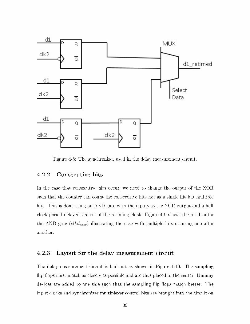
Figure 4-8: The synchronizer used in the delay measurement circuit.
4.2.2 Consecutive hits
In the case that consecutive hits occur, we need to change the output of the XOR
such that the counter can count the consecutive hits not as a single hit but multiple
hits. This is done using an AND gate with the inputs as the XOR output and a half
clock period delayed version of the retiming clock. Figure 4-9 shows the result after
the AND gate (𝑐𝑙𝑘𝑑𝑣𝑥𝑜𝑟) illustrating the case with multiple hits occuring one after
another.
4.2.3 Layout for the delay measurement circuit
The delay measurement circuit is laid out as shown in Figure 4-10. The sampling
flip-flops must match as closely as possible and are thus placed in the center. Dummy
devices are added to one side such that the sampling flip flops match better. The
input clocks and synchronizer multiplexer control bits are brought into the circuit on
39
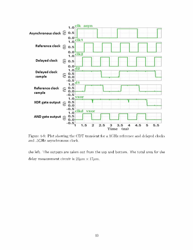
Figure 4-9: Plot showing the CDT transient for a 1GHz reference and delayed clocksand .5GHz asynchronous clock.
the left. The outputs are taken out from the top and bottom. The total area for the
delay measurement circuit is 23𝜇𝑚× 17𝜇𝑚.
40
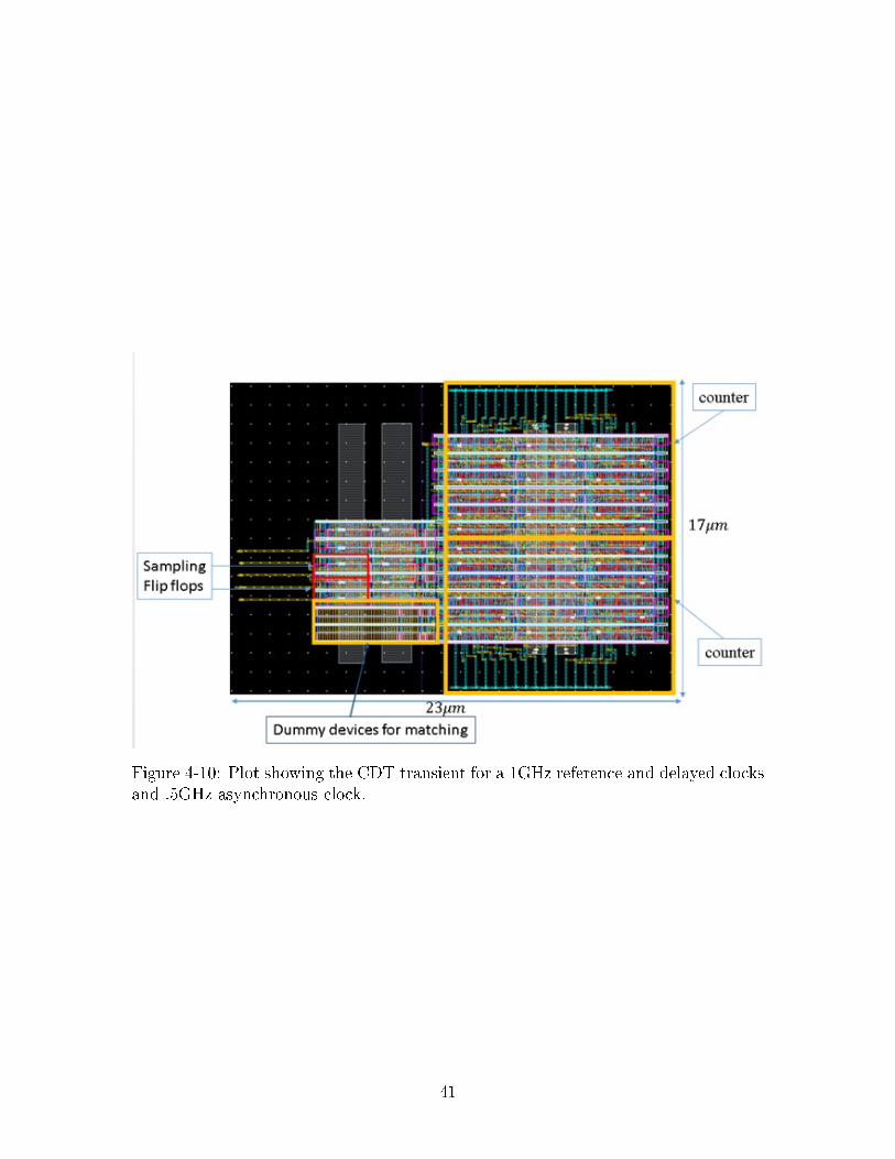
Figure 4-10: Plot showing the CDT transient for a 1GHz reference and delayed clocksand .5GHz asynchronous clock.
41

42

Chapter 5
PTAT Current Generation
The PTAT current is generated by the circuit shown in Figure 5-1. In the circuit, all
the devices operate in sub-threshold regime. The devices 𝑀3 and 𝑀4 have the same
size and carry the same current. 𝑀1 and 𝑀2 operate at the same current due to
the 1:1 current mirror formed by 𝑀3 and 𝑀4. Since the source of 𝑀2 is connected
to ground while that of 𝑀1 is connected to a resistor in order for the two devices
to carry the same current 𝑀1 is sized larger than 𝑀2. The difference in the 𝑉𝐺𝑆 of
𝑀1 and 𝑀2 produces a voltage 𝑉𝑃𝑇𝐴𝑇 proportional to temperature. If the resistor
has a small temperature coefficient, the output current will be proportional to the
temperature.
The output current can be determined by deriving an equation for the voltage
across the resistor. Consider 𝑀1 and 𝑀2 which have the same current and are
operating in sub-threshold regime. Following the analysis from [16], we can write,
𝑖𝑀1 ≈ 𝐼𝑂𝑆,1𝑒(𝑞
𝑉𝐺𝑆1−𝑉𝑇𝑛𝑘𝑇
)(1 − 𝑒−𝑞𝑉𝐷𝑆1
𝑘𝑇 ) (5.1)
where
𝐼𝑂𝑆,1 =𝑊1
𝐿1
𝜇𝐶𝑂𝑋(𝑘𝑇
𝑞)2(𝑛− 1) (5.2)
Similarly for M2,
𝑖𝑀2 ≈ 𝐼𝑂𝑆,2𝑒(𝑞
𝑉𝐺𝑆2−𝑉𝑇𝑛𝑘𝑇
)(1 − 𝑒−𝑞𝑉𝐷𝑆2
𝑘𝑇 ) (5.3)
43
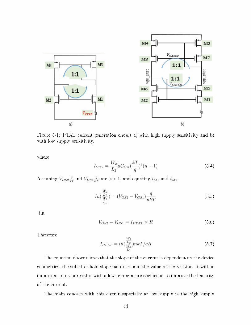
Figure 5-1: PTAT current generation circuit a) with high supply sensitivity and b)with low supply sensitivity.
where
𝐼𝑂𝑆,2 =𝑊2
𝐿2
𝜇𝐶𝑂𝑋(𝑘𝑇
𝑞)2(𝑛− 1) (5.4)
Assuming 𝑉𝐷𝑆2𝑞𝑘𝑇and 𝑉𝐷𝑆1
𝑞𝑘𝑇
are >> 1, and equating 𝑖𝑀1 and 𝑖𝑀2.
𝑙𝑛(𝑊2
𝐿2
𝑊1
𝐿1
) = (𝑉𝐺𝑆2 − 𝑉𝐺𝑆1)𝑞
𝑛𝑘𝑇(5.5)
But
𝑉𝐺𝑆2 − 𝑉𝐺𝑆1 = 𝐼𝑃𝑇𝐴𝑇 ×𝑅 (5.6)
Therefore
𝐼𝑃𝑇𝐴𝑇 = 𝑙𝑛(𝑊2
𝐿2
𝑊1
𝐿1
)𝑛𝑘𝑇/𝑞𝑅 (5.7)
The equation above shows that the slope of the current is dependent on the device
geometries, the sub-threshold slope factor, n, and the value of the resistor. It will be
important to use a resistor with a low temperature coefficient to improve the linearity
of the current.
The main concern with this circuit especially at low supply is the high supply
44

sensitivity. In order to improve the supply rejection, the current mirrors are cascoded
as shown in Figure 5-1 b. The design of the cascode current mirrors requires the
generation of two bias voltages, 𝑉𝐶𝐴𝑆𝐶𝑁 and 𝑉𝐶𝐴𝑆𝐶𝑃 . The circuit used to generate
the bias is shown in Figure 5-2. The bias circuitry is designed to have 14of the current
in the PTAT generator circuit. Thus MP1, MP2 and MN2 are designed to have the
same length and 14the width of M3 ,M7 and M2 respectively. Similarly MN2, MP3
are scaled to have an overdrive voltage matched to that of the cascode device M6,
and M7 respectively. The size of M3 and M4 is 100𝜇𝑚450𝑛𝑚
. M5-8 are sized as 100𝜇𝑚150𝑛𝑚
. M1
is sized as 100𝜇𝑚450𝑛𝑚
while M2 is sized as 25𝜇𝑚450𝑛𝑚
. The resistor is picked to be 500Ω.
Figure 5-2: The bias circuitry for the PTAT current generator. The vcascp biasgenerator current source is not cascoded due to the low value of voltage and hencelow headroom for the current source MN1.
In order for this circuit to have good supply rejection, all devices must operate
45
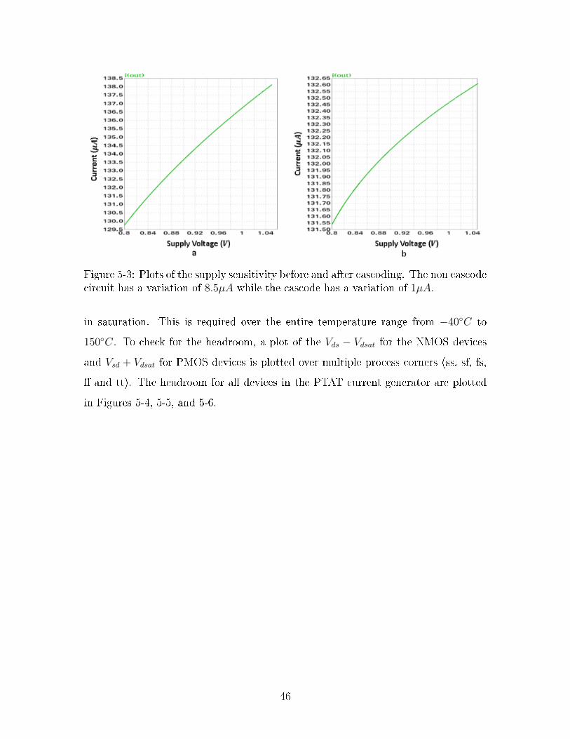
Figure 5-3: Plots of the supply sensitivity before and after cascoding. The non cascodecircuit has a variation of 8.5𝜇𝐴 while the cascode has a variation of 1𝜇𝐴.
in saturation. This is required over the entire temperature range from −40∘𝐶 to
150∘𝐶. To check for the headroom, a plot of the 𝑉𝑑𝑠 − 𝑉𝑑𝑠𝑎𝑡 for the NMOS devices
and 𝑉𝑠𝑑 + 𝑉𝑑𝑠𝑎𝑡 for PMOS devices is plotted over multiple process corners (ss, sf, fs,
ff and tt). The headroom for all devices in the PTAT current generator are plotted
in Figures 5-4, 5-5, and 5-6.
46
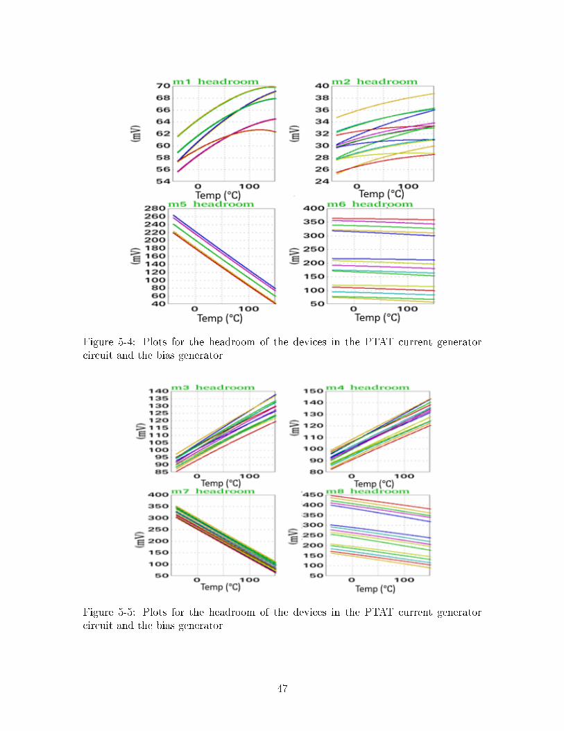
Figure 5-4: Plots for the headroom of the devices in the PTAT current generatorcircuit and the bias generator
Figure 5-5: Plots for the headroom of the devices in the PTAT current generatorcircuit and the bias generator
47
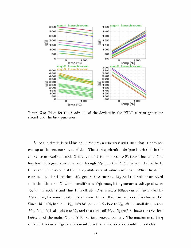
Figure 5-6: Plots for the headroom of the devices in the PTAT current generatorcircuit and the bias generator
Since the circuit is self-biasing, it requires a startup circuit such that it does not
end up at the zero current condition. The startup circuit is designed such that in the
zero current condition node X in Figure 5-7 is low (close to 0V) and thus node Y is
low too. This generates a current through 𝑀𝑌 into the PTAT circuit. By feedback,
the current increases until the steady state current value is achieved. When the stable
current condition is reached, 𝑀𝑋 generates a current. 𝑀𝑋 and the resistor are sized
such that the node X at this condition is high enough to generate a voltage close to
𝑉𝑑𝑑 at the node Y and thus turn off 𝑀𝑌 . Assuming a 100𝜇𝐴 current generated by
𝑀𝑋 during the non-zero stable condition. For a 10𝑘Ω resistor, node X is close to 1V.
Since this is higher than 𝑉𝑑𝑑, this brings node X close to 𝑉𝑑𝑑 with a small drop across
𝑀𝑋 . Node Y is also close to 𝑉𝑑𝑑 and this turns off 𝑀𝑌 . Figure 5-6 shows the transient
behavior of the nodes X and Y for various process corners. The maximum settling
time for the current generator circuit into the nonzero stable condition is 650ns.
48
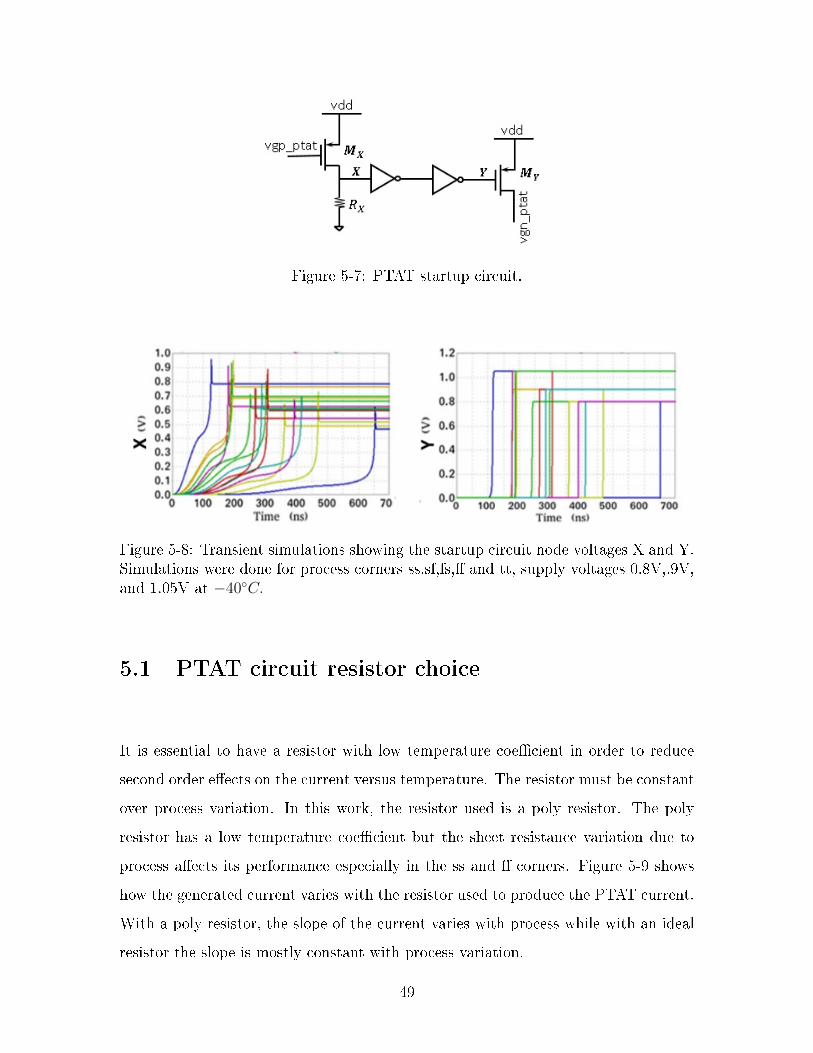
Figure 5-7: PTAT startup circuit.
Figure 5-8: Transient simulations showing the startup circuit node voltages X and Y.Simulations were done for process corners ss,sf,fs,ff and tt, supply voltages 0.8V,.9V,and 1.05V at −40∘𝐶.
5.1 PTAT circuit resistor choice
It is essential to have a resistor with low temperature coefficient in order to reduce
second order effects on the current versus temperature. The resistor must be constant
over process variation. In this work, the resistor used is a poly resistor. The poly
resistor has a low temperature coefficient but the sheet resistance variation due to
process affects its performance especially in the ss and ff corners. Figure 5-9 shows
how the generated current varies with the resistor used to produce the PTAT current.
With a poly resistor, the slope of the current varies with process while with an ideal
resistor the slope is mostly constant with process variation.
49
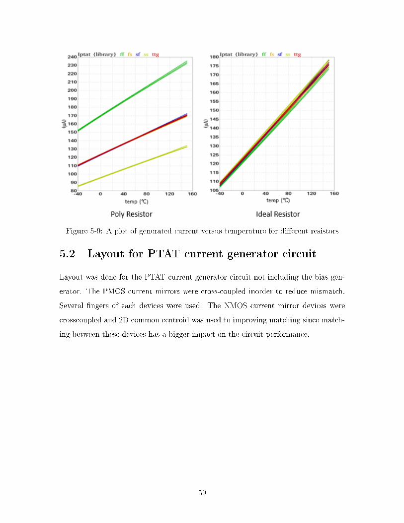
Figure 5-9: A plot of generated current versus temperature for different resistors
5.2 Layout for PTAT current generator circuit
Layout was done for the PTAT current generator circuit not including the bias gen-
erator. The PMOS current mirrors were cross-coupled inorder to reduce mismatch.
Several fingers of each devices were used. The NMOS current mirror devices were
crosscoupled and 2D common centroid was used to improving matching since match-
ing between these devices has a bigger impact on the circuit performance.
50
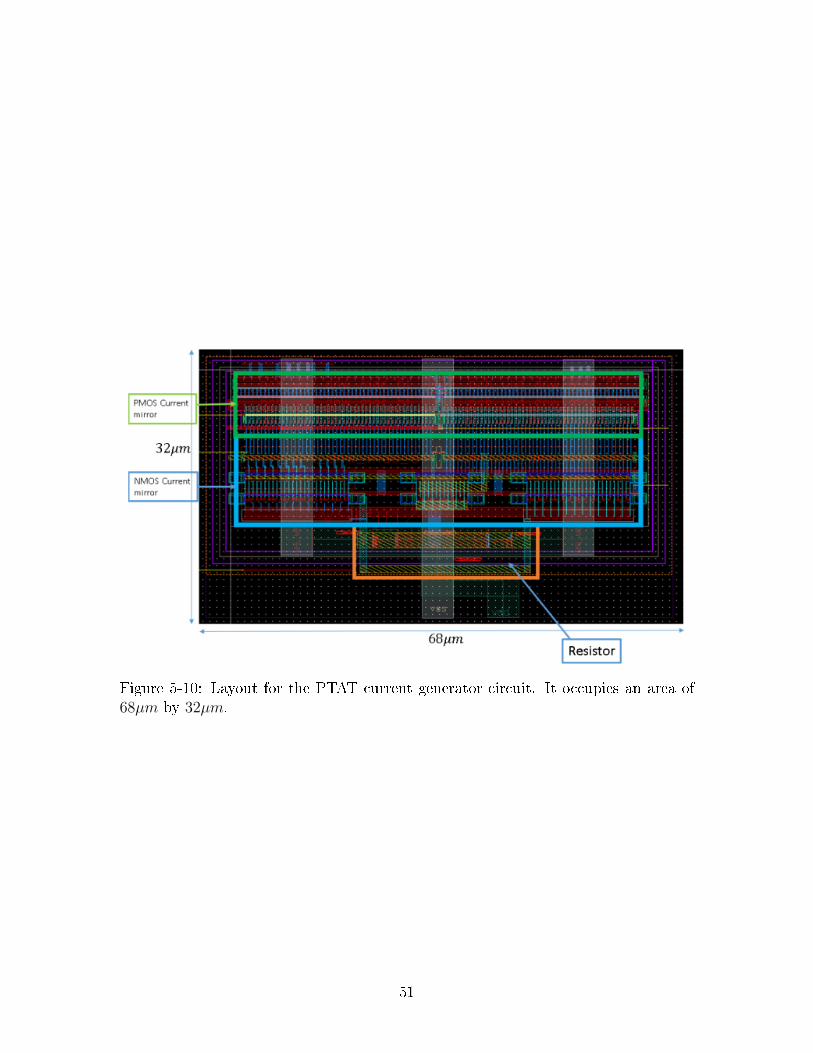
Figure 5-10: Layout for the PTAT current generator circuit. It occupies an area of68𝜇𝑚 by 32𝜇𝑚.
51

52
Chapter 6
Dual Slope Circuit
The dual slope circuit works similarly to a dual slope analog-to-digital converter.
In this case, a capacitor is charged and discharged using two currents. The charging
current is PTAT (proportional to the absolute temperature). The discharging current
has an almost zero temperature coefficient and is often defined as a ZTAT current.
The operation of the circuit consists of 3 phases: reset, charging, and discharging.
The initial phase is the reset mode where the capacitor voltage is set to a reference
voltage. The next phase is the charging mode where the capacitor is charged by a
current proportional to the temperature. The last phase is the discharge phase where
the capacitor is discharged through a current constant with temperature until its
voltage is equal to the reference voltage. Once this occurs, a comparator will trip
from low to high creating the rising edge of a clock waveform seen at its output.
6.1 Operation of the Dual Slope circuit
A simplified diagram of the Dual Slope circuit is shown in Figure 6-1. As previously
mentioned, the circuit operates in three phases. During the first phase that lasts for
an entire clock period, the capacitor plate is reset to a reference voltage, 𝑉𝑟𝑒𝑓 . In
the next phase, the capacitor is charged by a PTAT current for half a clock period.
Finally, in the last phase the capacitor is discharged through a ZTAT current until
its voltage crosses 𝑉𝑟𝑒𝑓 .
53
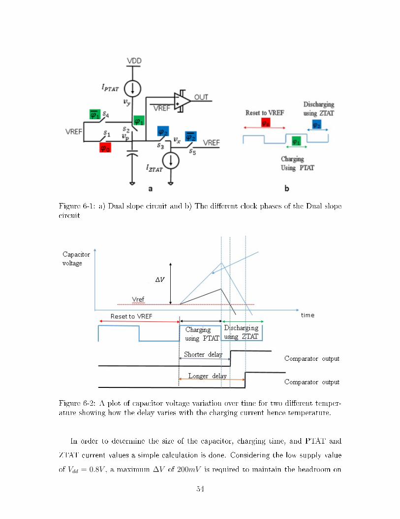
Figure 6-1: a) Dual slope circuit and b) The different clock phases of the Dual slopecircuit
Figure 6-2: A plot of capacitor voltage variation over time for two different temper-ature showing how the delay varies with the charging current hence temperature.
In order to determine the size of the capacitor, charging time, and PTAT and
ZTAT current values a simple calculation is done. Considering the low supply value
of 𝑉𝑑𝑑 = 0.8𝑉 , a maximum ∆𝑉 of 200𝑚𝑉 is required to maintain the headroom on
54
all the current sources. From simulations, the PTAT current varies from 105𝜇𝐴 at
−40∘𝐶 to about 170𝜇𝐴 125∘𝐶. In order to reduce power consumption, this current is
divided down by a factor of 4. As a starting point, the clock period, T was chosen to
be 1𝑛𝑠. Therefore, the maximum 𝐷𝑒𝑙𝑡𝑎𝑉 , ∆𝑉𝑚𝑎𝑥 = 𝐼𝑚𝑎𝑥
𝐶𝑇/2 can be used to estimate
the capacitor value, C. Using the values estimated, the capacitor value is estimated
to be 100fF. In simulations, the clock frequency of 1GHz turned out to be too fast
and thus was reduced by a factor of 4. Reducing the clock frequency by 4 required
increasing the capacitor size by 4 or reducing the current by a factor of 4 for the same
∆𝑉𝑚𝑎𝑥 = 𝐼𝑚𝑎𝑥
𝐶. Increasing the capacitor size by 4 is the better option since decreasing
the current by 4 requires reducing the size of the PTAT current mirror which degrades
the accuracy of the current from the current mirror. Therefore a capacitor of 400fF
is selected. The reference clock frequency is also selected to be 250MHz.
It is important to make sure that the switch voltages are close to the capacitor
voltage right before the switch is turned on. The bigger the difference between the
nodes 𝑣𝑥 and 𝑣𝑦 from the capacitor voltage, the higher the error in the delay versus
temperature plot. This is because the capacitor voltage increases nonlinearly until
the node 𝑣𝑦 or 𝑣𝑥 follows the capacitor voltage.
Although the switch, S4 was trying to tie 𝑣𝑦 to 𝑉𝑟𝑒𝑓 = 𝑉𝑑𝑑
2in this case, 𝑣𝑦 turned
out higher due to the low switch 𝑉𝑔𝑠 and thus required a higher 𝑉𝑑𝑠 for the same
current. This implies that there is a large drop across the switch. In order to reduce
the switch drop 𝑉𝑟𝑒𝑓 is set to 𝑉𝑑𝑑
2− 100𝑚𝑉 instead of 𝑉𝑑𝑑
2and thus 𝑉𝑔𝑠 is increased.
The drop across the switch is now reduced and right before switching the voltage at
the node 𝑣𝑦 is close to the capacitor voltage. Another way of explaining why reducing
𝑉𝑟𝑒𝑓 makes 𝑣𝑦 closer to 𝑉𝑟𝑒𝑓 is because the increase in 𝑉𝑔𝑠 of S4 leads to a smaller
switch on-resistance.
In Figure 6-5, at 3ns the discharge switch is turned on. When the switch closes,
the node 𝑣𝑥 is rapidly pulled up to 𝑣𝑝. This switch transition region is shown in
Figure 6-5 as the region between the two red lines. The node voltage 𝑣𝑥 following 𝑣𝑝
is non-ideal since this results in charge-sharing. The smaller the switch on resistance
the faster that 𝑣𝑥 follows 𝑣𝑝 and thus the smaller the error introduced due to the
55
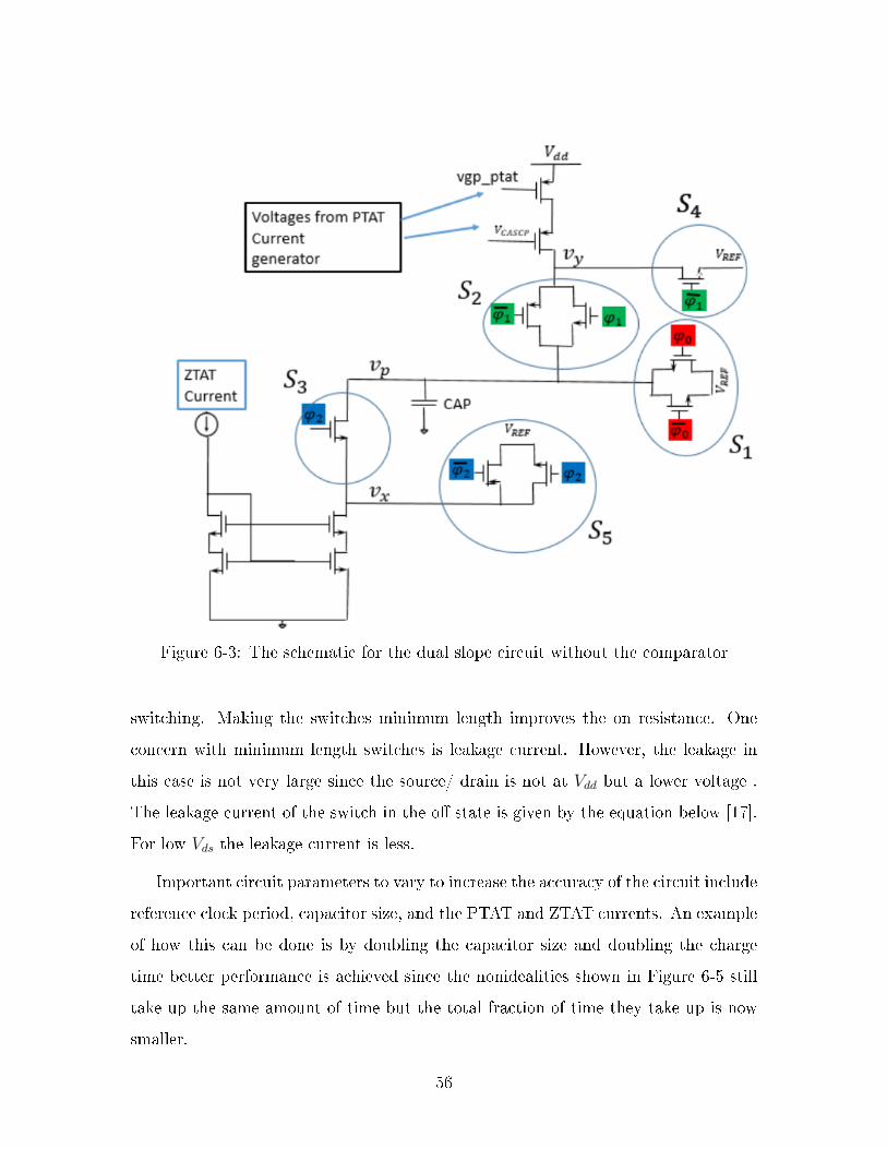
Figure 6-3: The schematic for the dual slope circuit without the comparator
switching. Making the switches minimum length improves the on resistance. One
concern with minimum length switches is leakage current. However, the leakage in
this case is not very large since the source/ drain is not at 𝑉𝑑𝑑 but a lower voltage .
The leakage current of the switch in the off state is given by the equation below [17].
For low 𝑉𝑑𝑠 the leakage current is less.
Important circuit parameters to vary to increase the accuracy of the circuit include
reference clock period, capacitor size, and the PTAT and ZTAT currents. An example
of how this can be done is by doubling the capacitor size and doubling the charge
time better performance is achieved since the nonidealities shown in Figure 6-5 still
take up the same amount of time but the total fraction of time they take up is now
smaller.
56
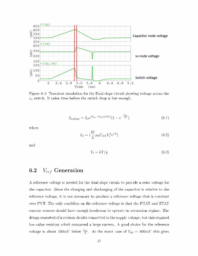
Figure 6-4: Transient simulation for the Dual slope circuit showing voltage across the𝑣𝑥 switch. It takes time before the switch drop is low enough.
𝐼𝑙𝑒𝑎𝑘𝑎𝑔𝑒 = 𝐼𝑂𝑒(𝑉𝑔𝑠−𝑉𝑡ℎ)/(𝑛𝑉𝑡)(1 − 𝑒
−𝑉𝑑𝑠𝑉𝑡 ) (6.1)
where
𝐼𝑂 = (𝑊
𝐿𝜇0𝐶𝑂𝑋𝑉
2𝑡 𝑒
1.8) (6.2)
and
𝑉𝑡 = 𝑘𝑇/𝑞 (6.3)
6.2 𝑉𝑟𝑒𝑓 Generation
A reference voltage is needed for the dual slope circuit to provide a reset voltage for
the capacitor. Since the charging and discharging of the capacitor is relative to the
reference voltage, it is not necessary to produce a reference voltage that is constant
over PVT. The only condition on the reference voltage is that the PTAT and ZTAT
current sources should have enough headroom to operate in saturation regime. The
design consisted of a resistor divider connected to the supply voltage, but this required
low-value resistors which consumed a large current. A good choice for the reference
voltage is about 100𝑚𝑉 below 𝑉𝑑𝑑
2. At the worst case of 𝑉𝑑𝑑 = 800𝑚𝑉 this gives
57
𝑉𝑟𝑒𝑓 = 300𝑚𝑉 . Suppose at maximum PTAT current the change in capacitor voltage
is 200𝑚𝑉 , this implies that the current source has at least 300𝑚𝑉 drop across it
which is sufficient for headroom. The design of the reference voltage was done using
a resistor divider. 𝑉𝑟𝑒𝑓 = 25𝑉𝑑𝑑, which gives a value close to the initial guess for 𝑉𝑟𝑒𝑓 .
6.3 Selection of switches
There are three possible switch types that can be selected; nMOS, pMOS, and comple-
mentary switch. The selection of the switch depends on the node voltages. Consider
for example node 𝑣𝑦. Node 𝑣𝑥 is initially set to a value close to reference voltage,𝑉𝑟𝑒𝑓
which is about 100𝑚𝑉 below 𝑉𝑑𝑑
2. The capacitor voltage,𝑣𝑝 is also set to the same
voltage. The node 𝑣𝑝 is then charged using the PTAT current and using estimate
calculation the change in capacitor voltage, ∆𝑉 is set to be less than 200𝑚𝑉 . At the
worst case when 𝑉𝑑𝑑 = 0.8𝑉 , this gives a maximum 𝑣𝑦 ≈ 500𝑚𝑉 . Thus 𝑣𝑦 varies from
300𝑚𝑉 to 500𝑚𝑉 . Although either only an nMOS or only pMOS switch could be
used, a complementary switch is preferred since the complementary switch has lower
charge injection into the capacitor. This is because some of the charge injected by the
nMOS is absorbed by the pMOS. Consider now the node 𝑣𝑥 which varies from 𝑉𝑟𝑒𝑓
when the ZTAT current is off to about 100𝑚𝑉 below 𝑉𝑟𝑒𝑓 during discharge. Since
this node voltage is low, an nMOS switch is sufficient since enough 𝑉𝑔𝑠 may be ap-
plied across it to provide sufficiently low on-resistance. In fact, a pMOS device will
degrade performance. The reset switch S1 is made to be a complementary switch to
reduce charge injection. Also the switch used to tie the node 𝑣𝑥 to 𝑉𝑟𝑒𝑓 is made to
be complementary. When the ZTAT and PTAT currents are off, the nodes 𝑣𝑥 and 𝑣𝑦
need to be set to appropriate voltages such that when the current is turned on less
time is taken charging the capacitance at the nodes 𝑣𝑦 and 𝑣𝑥 . If the time taken to
charge or discharge the capacitance at 𝑣𝑥 and 𝑣𝑦 is long, the accuracy of the circuit
is degraded similar to what was explained in Figure 6-5.
58
6.4 Comparator
6.4.1 Comparator Design
There are several parameters to consider in the design of the comparator for our cir-
cuit. The most essential are the gain, propagation delay, and offset voltage variation.
The comparator must have a very low offset variation with temperature in order to
avoid errors as the temperature changes. The gain of the comparator has to be high
enough in order to compare small differences in the input differential signal and pro-
duce a full-swing CMOS level output. Since the capacitor voltage is a ramp with an
inherently low slew rate, if the gain is low, the delay before the comparator output
changes is high. This delay also has a large variation with PVT. This affects the
accuracy of the output of the comparator. Simulations were run to determine how
much gain can be achieved for a given current density for a resistor-loaded differential
pair
The comparator consists of 3 differential stages followed by a single ended to dif-
ferential stage. After the single-ended to differential conversion, a cascade of two
inverters is used to increase the slew rate of the output. The differential stage is
designed using a PMOS differential pair. PMOS devices are used since the input
common mode is approximately 300𝑚𝑉 and would be too low for an NMOS differen-
tial pair to operate in saturation. The devices are minimum length in order to achieve
high bandwidth and have a low enough propagation delay. Resistors are used as the
load for the differential in order to reduce mismatch among the stages. A single stage
of the differential stage is shown in Figure 6-6.
For the initial design, the source current was 200𝜇𝐴 and the load resistor was
4𝑘Ω. The current sources are PMOS devices of length 150𝑛𝑚 and width 100𝜇𝑚. The
input differential PMOS devices had a length of 35𝑛𝑚 and a width of 16𝜇𝑚.This
results in an output common mode of 100𝜇𝐴 × 4𝑘Ω = 0.4𝑉 . The 0.4𝑉 enables DC
coupling to the next differential stage. In order to increase the bandwidth, the load
resistor of 4𝑘Ω is reduced to 3.5𝑘Ω. From simulations the transconductance, 𝑔𝑚 of
each stage was about 1.5𝑚𝑆 . The output impedance of each of the input devices
59
Figure 6-5: A differential amplifier with resistor loads.
given by 𝑟𝑜 = 1/𝑔𝑑𝑠 = 1/200𝜇 = 5𝑘Ω. The gain per stage, 𝐺 = 𝑔𝑚1
(𝑔𝑑𝑠+1/𝑅𝐿). This
gives a value of about 3.5
Figure 6-6: The full comparator excluding the output of the inverter stages.
The gain at the output of each stage of the comparator is shown in Figure 6-8.
Each of the differential stages has a gain of approximately 3.5. Due to the ac coupling
a band pass filter is created by the coupling capacitor and the input resistance of the
inverter with feedback. It is important to have the low frequency cut off below
the frequency of operation. This is done by either increasing the capacitor value or
60
increasing the resistor value. 𝑓𝑙𝑜𝑤 = 12×𝜋×𝑅𝑖𝑛×𝐶𝐶
where 𝐶𝐶 is the coupling capacitor
and 𝑅𝑖𝑛 is the input resistance of the inverter with the feedback resistor. With a
200𝑓𝐹 capacitor and 155𝑘Ω feedback resistor gives a 74𝑀𝐻𝑧 low cutoff frequency.
Figure 6-7: The output stage of the comparator consisting of ac coupled feedbackinverter followed by two inverter stages.
Figure 6-8: The gain at the output of each amplifier stage of the comparator. The accoupling implements a band pass filter with a low cut off close to 100MHz
61
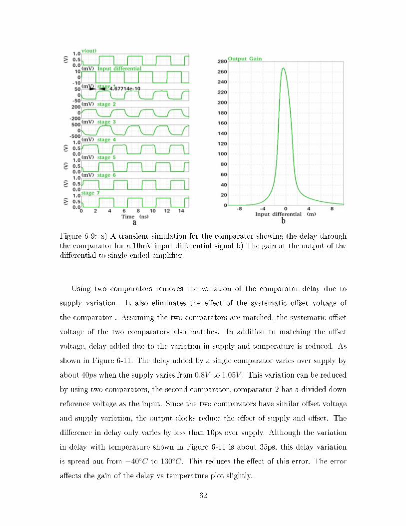
Figure 6-9: a) A transient simulation for the comparator showing the delay throughthe comparator for a 10mV input differential signal b) The gain at the output of thedifferential to single ended amplifier.
Using two comparators removes the variation of the comparator delay due to
supply variation. It also eliminates the effect of the systematic offset voltage of
the comparator . Assuming the two comparators are matched, the systematic offset
voltage of the two comparators also matches. In addition to matching the offset
voltage, delay added due to the variation in supply and temperature is reduced. As
shown in Figure 6-11. The delay added by a single comparator varies over supply by
about 40𝑝𝑠 when the supply varies from 0.8𝑉 to 1.05𝑉 . This variation can be reduced
by using two comparators, the second comparator, comparator 2 has a divided down
reference voltage as the input. Since the two comparators have similar offset voltage
and supply variation, the output clocks reduce the effect of supply and offset. The
difference in delay only varies by less than 10ps over supply. Although the variation
in delay with temperature shown in Figure 6-11 is about 35ps, this delay variation
is spread out from −40∘𝐶 to 130∘𝐶. This reduces the effect of this error. The error
affects the gain of the delay vs temperature plot slightly.
62
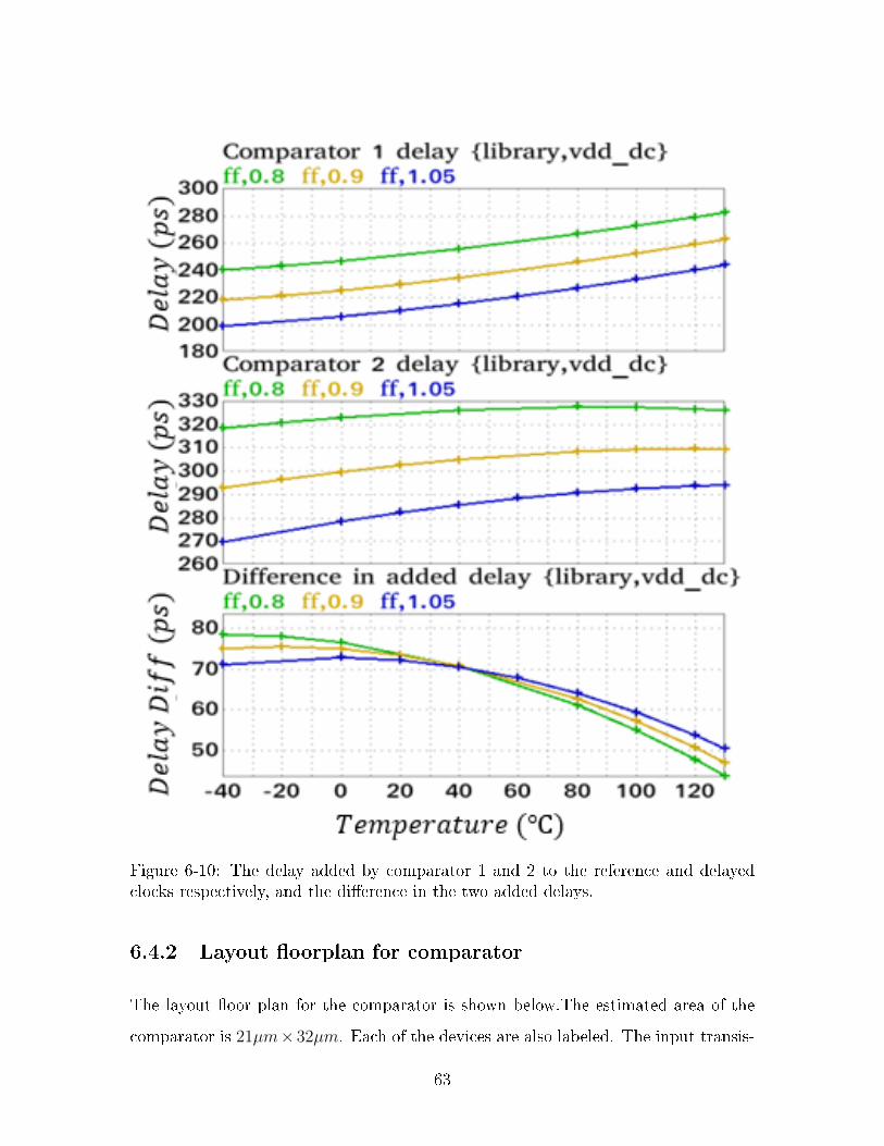
Figure 6-10: The delay added by comparator 1 and 2 to the reference and delayedclocks respectively, and the difference in the two added delays.
6.4.2 Layout floorplan for comparator
The layout floor plan for the comparator is shown below.The estimated area of the
comparator is 21𝜇𝑚× 32𝜇𝑚. Each of the devices are also labeled. The input transis-
63
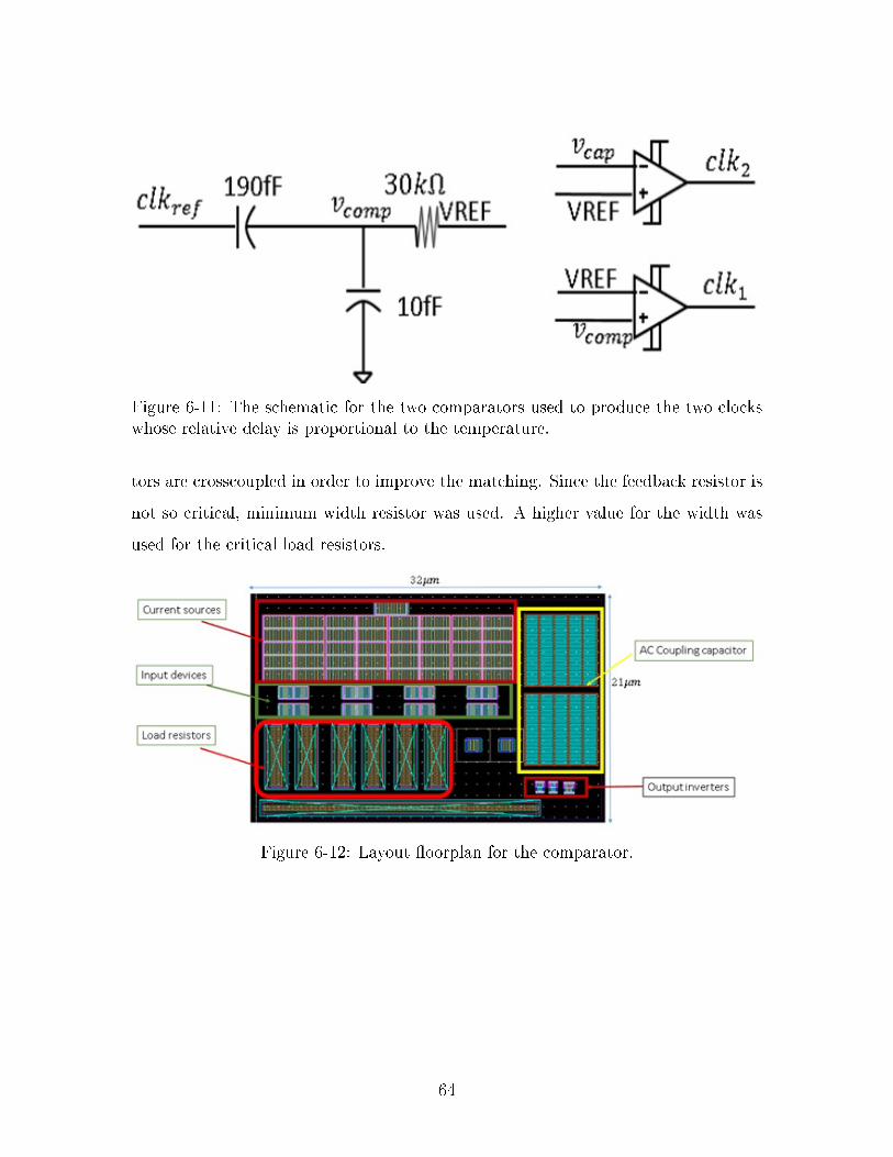
Figure 6-11: The schematic for the two comparators used to produce the two clockswhose relative delay is proportional to the temperature.
tors are crosscoupled in order to improve the matching. Since the feedback resistor is
not so critical, minimum width resistor was used. A higher value for the width was
used for the critical load resistors.
Figure 6-12: Layout floorplan for the comparator.
64
Chapter 7
Results and Calibration
7.1 Power consumption and area of the delay and
temperature measurement systems
The area from the layout of the PTAT current generator circuit is 68𝜇𝑚 × 32𝜇𝑚 ≈
2200𝜇𝑚2. The PTAT bias generator circuit was estimated to be 200𝜇𝑚2. The floor
plan for the comparator used in the dual slope circuit is estimated to be 32𝜇𝑚 ×
21𝜇𝑚 = 672𝜇𝑚2. For two comparators and accounting for the rest of the dual slope
circuit, the total area for the dual slope circuit is 1600𝜇𝑚2. The delay measurement
circuit (CDT circuit) occupies an area of 23𝜇𝑚×17𝜇𝑚 = 391𝜇𝑚2. This gives a total
area of 4391𝜇𝑚2.
The power consumption for the PTAT current generator varies with tempera-
ture. Using the highest current of 170𝜇𝐴, this gives a total power consumption
of 153𝜇𝑊 , at 0.9𝑉 supply. The dual slope circuit consumes a total current of
42.5𝜇𝐴+50𝜇𝐴 = 92.5𝜇𝐴. This gives a power consumption of 83.25𝜇𝑊 . This excludes
the logic, reference voltage generator and the comparator. The two comparators con-
sume 200𝜇𝐴 × 8𝜇𝐴 + 20𝜇𝐴 × 2 = 1640𝜇𝐴. This gives a total power consumption
of 1.5𝑚𝑊 . The reference voltage generator approximately 1𝑚𝑊 . This gives a to-
tal power consumption of 2.83𝑚𝑊 excluding the logic, and the delay measurement
circuit has a power consumption of 80𝜇𝑊 .
65
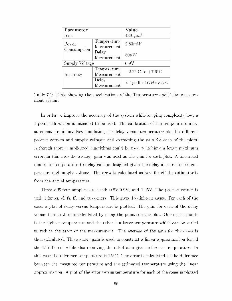
Parameter ValueArea 4391𝜇𝑚2
PowerConsumption
TemperatureMeasurement
2.83𝑚𝑊
DelayMeasurement
80𝜇𝑊
Supply Voltage 0.9V
AccuracyTemperatureMeasurement
−2.2∘ C to +7.6∘𝐶
DelayMeasurement
< 1𝑝𝑠 for 1𝐺𝐻𝑧 clock
Table 7.1: Table showing the specifications of the Temperature and Delay measure-ment system
In order to improve the accuracy of the system while keeping complexity low, a
1-point calibration is intended to be used. The calibration of the temperature mea-
surement circuit involves simulating the delay versus temperature plot for different
process corners and supply voltages and extracting the gain for each of the plots.
Although more complicated algorithms could be used to achieve a lower maximum
error, in this case the average gain was used as the gain for each plot. A linearized
model for temperature to delay can be designed given the delay at a reference tem-
perature and supply voltage. The error is calculated as how far off the estimator is
from the actual temperature.
Three different supplies are used; 0.8V,0.9V, and 1.05V. The process corner is
varied for ss, sf, fs, ff, and tt corners. This gives 15 different cases. For each of the
case, a plot of delay versus temperature is plotted. The gain for each of the delay
versus temperature is calculated by using the points on the plot. One of the points
is the highest temperature and the other is a lower temperature which can be varied
to reduce the error of the measurement. The average of the gain for the cases is
then calculated. The average gain is used to construct a linear approximation for all
the 15 different while also removing the offset at a given reference temperature. In
this case the reference temperature is 25∘𝐶. The error is calculated as the difference
between the measured temperature and the estimated temperature using the linear
approximation. A plot of the error versus temperature for each of the cases is plotted
66
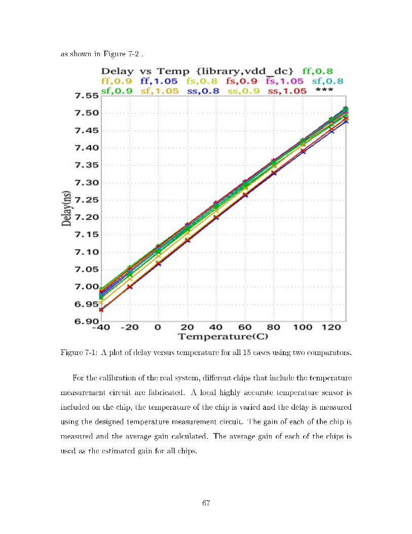
as shown in Figure 7-2 .
Figure 7-1: A plot of delay versus temperature for all 15 cases using two comparators.
For the calibration of the real system, different chips that include the temperature
measurement circuit are fabricated. A local highly accurate temperature sensor is
included on the chip, the temperature of the chip is varied and the delay is measured
using the designed temperature measurement circuit. The gain of each of the chip is
measured and the average gain calculated. The average gain of each of the chips is
used as the estimated gain for all chips.
67
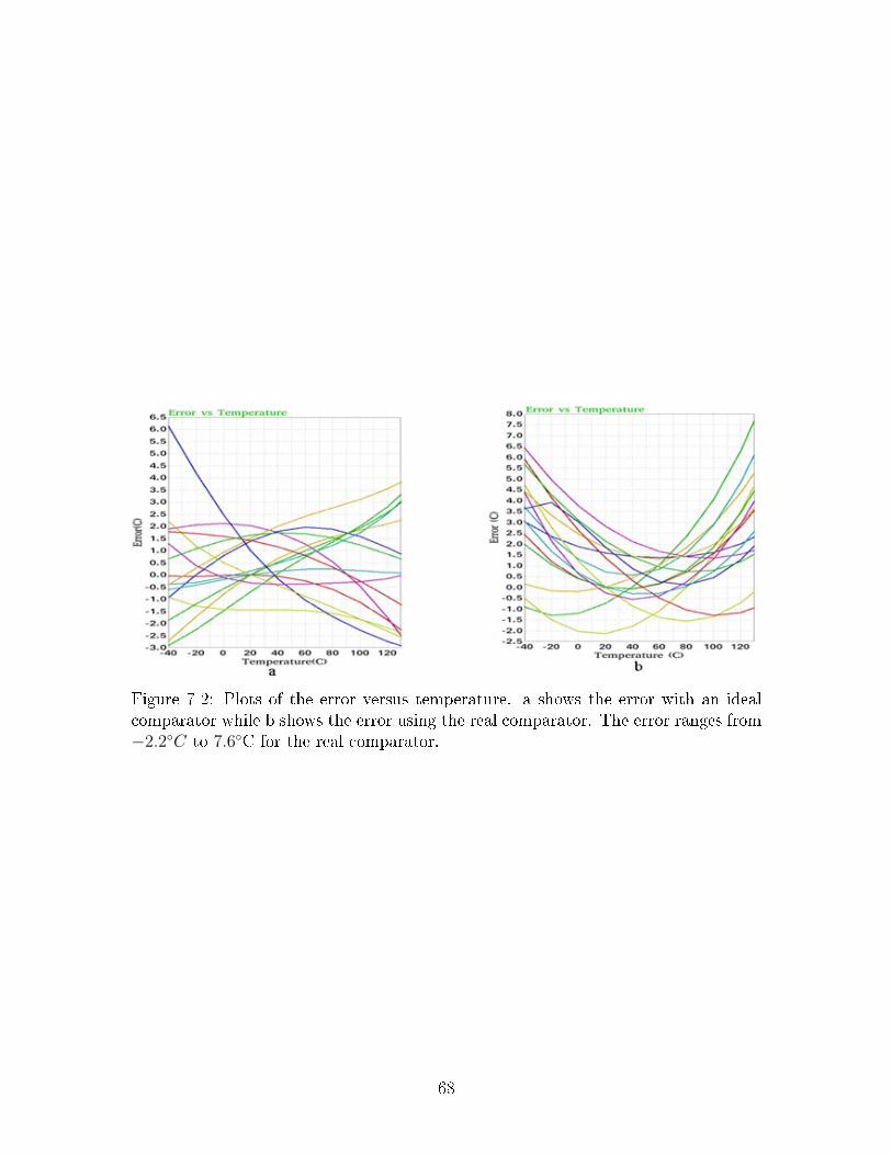
Figure 7-2: Plots of the error versus temperature. a shows the error with an idealcomparator while b shows the error using the real comparator. The error ranges from−2.2∘𝐶 to 7.6∘C for the real comparator.
68
Chapter 8
Future work and conclusion
The design and simulation of an on-chip temperature and delay measurement cir-
cuit is presented. The accuracy of the delay measurement system increased with
increased simulation time. Layout was done for the delay measurement circuit, and a
PTAT current generator circuit. In simulation, the temperature measurement circuit
can measure temperatures with an error of −2.2∘𝐶 to 7.6∘C over the range −40∘𝐶
to 130∘𝐶 across process and supply corners. This error doesn’t include the error
introduced by delay measurement system.
Possible future work include the design of a supply voltage measurement circuit,
which was explained in section 1. An all-digital temperature measurement circuit
can also be designed using DLL or ring oscillators. The use of digital circuits reduces
the complexity of the design and the area. The main issue with an all-digital tem-
perature measurement circuit is the low supply used makes it difficult to get a linear
relationship between delay and temperature.
69

70
Appendix A
Appendix
A.1 Circuit schematics
Figure A-1: Delay measurement circuit schematic
71
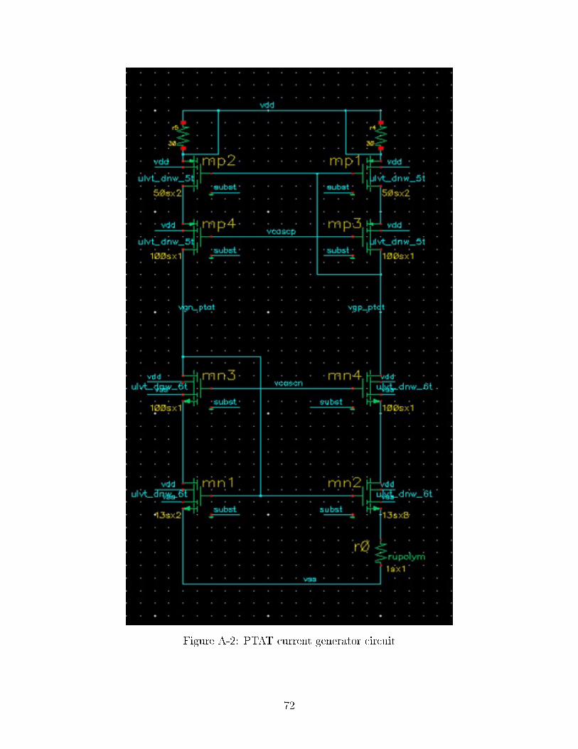
Figure A-2: PTAT current generator circuit
72
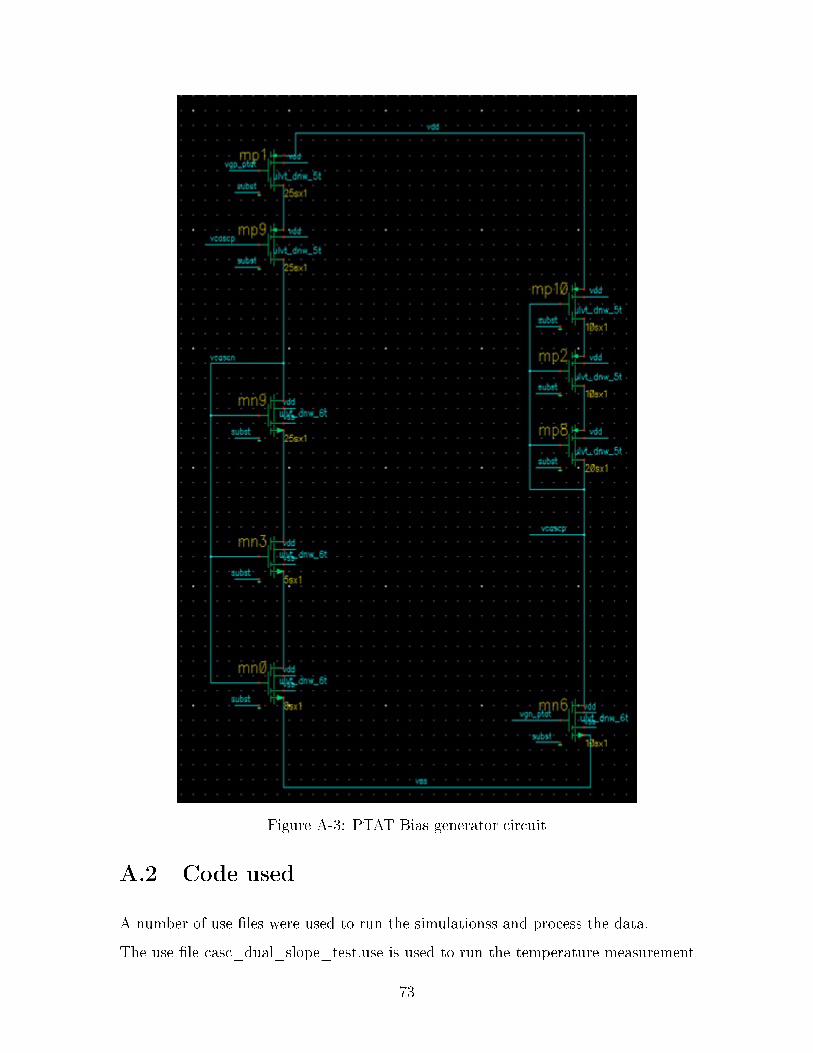
Figure A-3: PTAT Bias generator circuit
A.2 Code used
A number of use files were used to run the simulationss and process the data.
The use file casc_dual_slope_test.use is used to run the temperature measurement
73
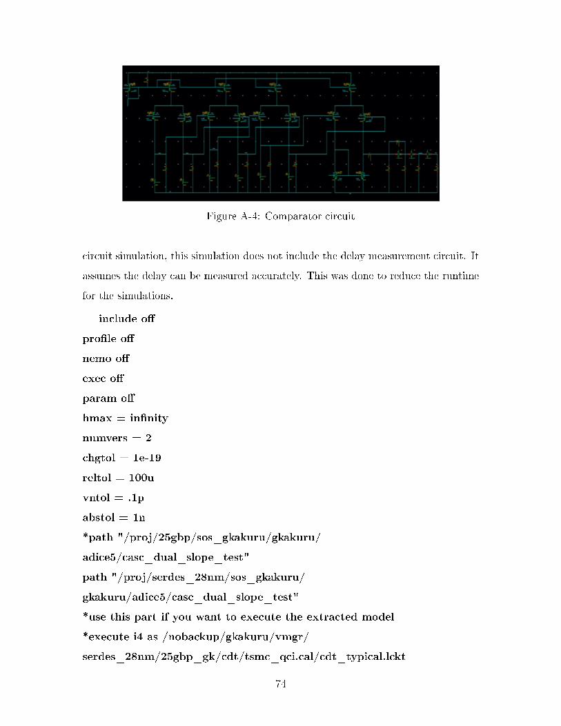
Figure A-4: Comparator circuit
circuit simulation, this simulation does not include the delay measurement circuit. It
assumes the delay can be measured accurately. This was done to reduce the runtime
for the simulations.
include off
profile off
nemo off
exec off
param off
hmax = infinity
numvers = 2
chgtol = 1e-19
reltol = 100u
vntol = .1p
abstol = 1n
*path "/proj/25gbp/sos_gkakuru/gkakuru/
adice5/casc_dual_slope_test"
path "/proj/serdes_28nm/sos_gkakuru/
gkakuru/adice5/casc_dual_slope_test"
*use this part if you want to execute the extracted model
*execute i4 as /nobackup/gkakuru/vmgr/
serdes_28nm/25gbp_gk/cdt/tsmc_qci.cal/cdt_typical.lckt
74

if (f10!=1) then
vdd_dc = 1.05
tdegc = 0
fclk=.25e9
skew all ss
ibias_dc=-40u
vn=.5
vpm=.2
capx=400f
vos=0
wx=2
fx=2
fn=8
numvers=3
nk=48
endif
*add rise and fall time to the reference clock
tr=15p
HIGH_VOLTAGE = vdd_dc
LOW_VOLTAGE = 0
UNKNOWN_VOLTAGE = HIGH_VOLTAGE/2
HIGH_THRESHOLD = HIGH_VOLTAGE/2
LOW_THRESHOLD = HIGH_VOLTAGE/2
keep all
sim casc_dual_slope_test
*sweep time from 0 to nk/fclk
sweep time from 0 to 187n
*sweep time from 0 to 1u
75
*sweep tdegc from 0 to 150
go
vclk_ref_half=v(vclk_ref_half)
vout=v(out1)
vcap=v(vp)
vref=v(vref)
d=find(v(cx),vdd_dc/2,1,1,5.5/fclk)-
find(v(outx),vdd_dc/2,1,2,5.5/fclk)
delay_clk=find(v(vclk_ref_half),
vdd_dc/2,1,1,31.95n)-32n
*delay_clk1=find(v(i13_z),vdd_dc/2,1,1,31.95n)-32n
delay_clk1=0
delay_clk2=find(v(vnx),vdd_dc/2,1,1,31.95n)-32n
dcomp1=find(v(cdt_clk1),vdd_dc/2,1,1,5.5/fclk)-
find(v(clk_ref_half),vdd_dc/2,1,1,5.5/fclk)
dcomp2=find(v(cdt_clk2),vdd_dc/2,1,1,5.5/fclk)-
find(v(vp,vref),0,-1,1,5.5/fclk+.2n)
m_comp1=find(v(cdt_clk2),vdd_dc/2,1,2,5.5/fclk)-
find(v(cx),vdd_dc/2,1,1,5.5/fclk)
*remember this is 1UI-delay
m_d=find(v(cdt_clk2),vdd_dc/2,1,2,5.5/fclk)-
find(v(cdt_clk1),vdd_dc/2,1,1,5.5/fclk)
m_d1=find(v(cdt_clk2),vdd_dc/2,1,2,17/fclk)-
find(v(cdt_clk1),vdd_dc/2,1,1,17/fclk)
m_d2=find(v(cdt_clk2),vdd_dc/2,1,2,18.5/fclk)-
76
find(v(cdt_clk1),vdd_dc/2,1,1,18.5/fclk)
m_d3=find(v(cdt_clk2),vdd_dc/2,1,2,38.5/fclk)-
find(v(cdt_clk1),vdd_dc/2,1,1,38.5/fclk)
Another important use file is the delay_circuit.use file, this file is used to run a
simulation of the delay measurement circuit, delay_circuit. The circuit includes a
behavioral model for the delay measurement circuit and the actual transistor model
for the same circuit designed using
standard cells. The input clock delay can be varied using the use file and the output
delay calculated.
include off
profile off
nemo off
exec off
param off
path off
nic off
path " /proj/25gbp/schem/
sos_gkakuru/jwalker/sim/use"
path "/proj/serdes_28nm/sos_gkakuru/
gkakuru/adice5/delay_circuit"
hmax = infinity
numvers = 2
chgtol = 1e-18
reltol = 100u
vntol = .1p
abstol = 1n
*in case you want to execute the extracted sim
*execute i0 as /nobackup/gkakuru/vmgr/
serdes_28nm/25gbp_gk/cdt/tsmc_qci.cal/cdt_typical.lckt
if (f10!=1) then
77
vdd_dc = .9
tdegc = 140
fclk=1e9
*fclk=.125e9
skew all ff
*delay=750p
*delay=7.6n
delay=.9n⁀
nk=10000
endif
fvco=500*(1+1/100)*1e6*.9
*v1 and v2 are the clock voltages
v1=0
v2=vdd_dc
tr=15p
HIGH_VOLTAGE = vdd_dc
LOW_VOLTAGE = 0
UNKNOWN_VOLTAGE = HIGH_VOLTAGE/2
HIGH_THRESHOLD = HIGH_VOLTAGE/2
LOW_THRESHOLD = HIGH_VOLTAGE/2
keep voltage
keep none
keep <i0> v(clk_asyn)
keep <i0> v(clk1)
keep <i0> v(clk2)
*keep <i0> v(d1)
*keep <i0> v(d2)
*keep <i0> v(rd1)
*keep <i0> v(rd2)
78
*keep <i0> v(dly_c1)
*keep <i0> v(vxor)
*keep <i0> v(clkd_vxor)
keep v(c_hits)
keep v(c_edges)
keep v(vf)
keep v(edges)
sim delay_circuit.ckt
sweep time from 0 to nk*1/fclk
go
vhits= v(c_hits)
ved= v(c_edges)
*added a small number to avoid 0/0
d=last(vhits+15.3e-6)*.5/(last(ved)+15.3e-6)*1/fclk
if (last(vhits)>.99) then
d=0
endif
err=(d-delay)
79

80
Bibliography
[1] F. O’Mahony and M. M. Bryan K. Casper.USA Patent PCT/US12/31408, 2012.
[2] M. A. P. Pertijs, K. ,. Makinwa and J. H. Huijsing, "A CMOS Smart Temperature
Sensor With a 3𝜎 Inaccuracy of 0.1 C From 55 C to 125 C," JSSC, 2005.
[3] C.-C. Chen, "A Time-to-Digital-Converter-Based CMOS Smart Temperature Sen-
sor," pp. 560-563, 2005.
[4] K. Woo, S. Meninger and Thucydides Xanthopoulos, "Dual-DLL-Based CMOS
All-Digital Temperature Sensor for Microprocessor Thermal Monitoring.," ISSCC,
2009.
[5] K. Kim, H. Lee and C. Kim, "366 − 𝑘𝑆/𝑠1.09 − 𝑛𝐽0.0013 −𝑚𝑚2 Frequency-to-
Digital Converter Based CMOS Temperature Sensor Utilizing Multiphase Clock,"
IEEE TRANSACTIONS ON VERY LARGE SCALE INTEGRATION SYS-
TEMS, vol. 21, no. 10, 2013.
[6] P. Chen, "A Time Domain Mixed-Mode Temperature Sensor with Digital Set-
Point Programming," CICC, 2006.
[7] D. Shim, "A Process-Variation-Tolerant On-Chip CMOS Thermometer for Auto
Temperature Compensated Self-Refresh of Low-Power Mobile DRAM," JSSC, pp.
2550-2557, 2013.
[8] I. M. Filanovsky and A. Allam, "Mutual Compensation of Mobility and Thresh-
old Voltage Temperature Effects with Applications in CMOS Circuits," IEEE
TRANSACTIONS ON CIRCUITS AND SYSTEMS, 2001.
81
[9] S.-W. Chen, M.-H. Chang, W.-C. Hsieh and a. W. Hwang, "Fully On-Chip Tem-
perature,Process and Voltage Sensor".
[10] F. O’Mahony, "On-chip timing and diagnostic circuits," SSCS, 2014.
[11] M. Mansuri, "An On-Die All-Digital Delay Measurement Circuit with 250fs Ac-
curacy," Symposium on VLSI Circuits Digest of Technical Papers, pp. 98-99, 2012.
[12] K. Bowman, "Dynamic Variation Monitor for Measuring the Impact of Voltage
Droops on Microprocessor Clock Frequency," CICC, 2010.
[13] J. Bergs, "Design of a VCO based ADC in 180nm for use in Positron Emission
Topography," 2010.
[14] S. Narendra, "Effect of Metal oxide semiconductor field-effect transistors thresh-
old voltage variation on high-performance circuits," MIT Thesis, pp. 25-30, 2002.
[15] I. A. Mahfuzul, "A Built-in Self-adjustment Scheme with Adaptive Body Bias
using P/N-sensitive Digital Monitor Circuits," IEEE Asian Solid-State Circuits
Conference, pp. 101-104, 2012.
[16] R. Sarpeshkar, Ultra Low Power Bioelectronics, 2011.
[17] P. F. B. Ribas and a. R. Perez, "Leakage Current in Sub-Micrometer CMOS
Gates".
[18] V. Abramzon, "Scalable Circuits for Supply Noise Measurement," ESSCIRC, pp.
463-466, 2005.
[19] E. Alon, V. Abramzon, B. Nazamfar and M. Horowitz, On-Die Power Supply
Noise Measurement Techniques, IEEE Transactions on Advanced Packaging, 2009.
82