DESIGN OF MULTIFUNCTIONAL MICROSTRIP …eprints.utar.edu.my/1475/1/ESA-2014-1201155-1.pdfDESIGN OF...
125
DESIGN OF MULTIFUNCTIONAL MICROSTRIP PATCH DIRECTIONAL COUPLERS AND STEPPED- IMPEDANCE SLOTLINE POWER DIVIDERS LIM SHENG LOKE MASTER OF ENGINEERING SCIENCE Faculty of Engineering and Science Universiti Tunku Abdul Rahman MAY 2014
-
Upload
vuongduong -
Category
Documents
-
view
232 -
download
3
Transcript of DESIGN OF MULTIFUNCTIONAL MICROSTRIP …eprints.utar.edu.my/1475/1/ESA-2014-1201155-1.pdfDESIGN OF...

DESIGN OF MULTIFUNCTIONAL MICROSTRIP
PATCH DIRECTIONAL COUPLERS AND STEPPED-
IMPEDANCE SLOTLINE POWER DIVIDERS
LIM SHENG LOKE
MASTER OF ENGINEERING SCIENCE
Faculty of Engineering and Science
Universiti Tunku Abdul Rahman
MAY 2014

ii
ABSTRACT
Microwave couplers are frequently used for designing various microwave
components such as filters, power dividers, phase shifters, etc. In the first part of
this thesis, several multifunctional power-dividing directional couplers that can
generate output signals with multiple levels are studied. Two passive power
dividers, working in the in-phase or out-of-phase operation, are first proposed.
Three rectangular microstrip patches are cascaded for the excitation of their
degenerate modes. By adding two extra output ports to the in-phase power divider,
it is interesting to note that the new multifunctional power-dividing directional
coupler is able to produce additional 10 and 20 dB coupled signals, both in-phase
and out-of-phase. This is the first demonstration, to the best of my knowledge, that
a single component can generate half-powered division as well as multiple (10 and
20 dB) coupled signals at the same time, leading to significant cost saving. In the
second part, the stepped-impedance slotline resonator has been deployed for
designing several passive in-phase and out-of-phase power dividers, which can be
made reconfigurable by incorporating RF PIN diodes at the output feedlines.
Reasonable agreement is observed between the simulated and measured results.

iii
ACKNOWLEDGEMENT
I would like to thank Dr. Lim Eng Hock and Dr. Lo Fook Loong for their directions,
ideas and guidance. Throughout the completion of this research project, invaluable
recommendations and suggestions have been shared. In addition, they were always
available whenever I have problems.
I also wish to thank Mr. Ho, who taught me the fabrication process. With
his guidance, I was able to make all my circuit boards. Besides that, I would also
like to extend my gratitude to all my seniors and friends for many useful
discussions.
I am thankful to UTAR for supporting all the necessary equipment,
facilities, and research materials. The online databases such as IEEE Xplore and
Microwave and Optical Technology Letters are very handy and helpful.

iv
APPROVAL SHEET
This thesis entitled ‘DESIGN OF MULTIFUNCTIONALMICROSTRIP
PATCH DIRECTIONAL COUPLERS AND STEPPED-
IMPEDANCESLOTLINE POWER DIVIDERS’ was prepared by LIM SHENG
LOKE and submitted as partial fulfillment of the requirement for the degree of
Master of Engineering Science at Universiti Tunku Abdul Rahman.
Approved by,
_________________________
(Dr. Lim Eng Hock) Date: ____________
Supervisor
Department of Electrical and Electronic Engineering
Faculty of Engineering Science
Universiti Tunku Abdul Rahman
_________________________
(Dr. Lo Fook Loong) Date: ____________
Co-supervisor
Department of Electrical and Electronic Engineering
Faculty of Engineering Science
Universiti Tunku Abdul Rahman

v
FACULTY OF ENGINEERING SCIENCE
UNIVERSITI TUNKU ABDUL RAHMAN
Date: _______________
SUBMISSION OF FINAL YEAR PROJECT /DISSERTATION /THESIS
It is hereby certified that LIM SHENG LOKE (ID No: 12 UEM 01155) has
completed this dissertation entitled “DESIGN OF MULTIFUNCTIONAL
MICROSTRIP PATCH DIRECTIONAL COUPLERS AND STEPPED-
IMPEDANCE SLOTLINE POWER DIVIDERS” under the supervision of Dr.
Lim Eng Hock (Supervisor) from the Department of Electrical and Electronic
Engineering, Faculty of Engineering and Science (FES), and Dr. Lo Fook
Loong(Co-Supervisor) from the Department of Electrical and Electronic
Engineering, Faculty of Engineering and Science (FES).
I understand that University will upload softcopy of my final dissertationinpdf
format into UTAR Institutional Repository, which may be made accessible to
UTAR community andpublic.
Yours truly,
____________________
(LIM SHENG LOKE)

vi
DECLARATION
I hereby declare that the thesis is based on my original work except for citations
and quotations which have been duly acknowledged. I also declare that it has not
been previously and concurrently submitted for any other degree or award at
UTAR or other institutions.
Name : LIM SHENG LOKE
Date : _________________

vii
TABLE OF CONTENTS
PAGE
ABSTRACT ii
ACKNOWLEDGEMENT iii
APPROVAL SHEET iv
SUBMISSION SHEET v
DECLARATION vi
TABLE OF CONTENTS vii
LIST OF TABLES x
LIST OF FIGURES xi
CHAPTER
1 INTRODUCTION 1
1.1 Background 1
1.2 Research Objectives and Motivation 3
1.3 Thesis Organization 3
2 LITERATURE REVIEW ON MICROWAVE COUPLER 5
2.1 Background and Introduction 5
2.1.1 Power Dividers and Directional Couplers 6
2.1.2 Microwave Resonators 7
2.2 Recent Developments of Power Dividers 9
2.2.1 Broadband and Dualband Power Dividers 9
2.2.2 Multifunctional Power Dividers 10
2.3 Recent Developments of Directional Couplers 11
2.3.1 Broadband Directional Couplers 11
2.3.2 Miniaturized Directional Couplers 12

viii
3 MULTIFUNCTIONAL POWER-DIVIDING DIRECTIONAL
COUPLERS WITH MULTIPLE OUTPUTS 13
3.1 Introduction 13
3.2 Design Methodology 15
3.3 Power Dividers 19
3.3.1 In-phase Power Divider 19
3.3.1.1 Simulation and Experiment Results 20
3.3.1.2 Theoretical and Parametric Studies 24
3.3.1.2.1 Widths of Patches W1 25
3.3.1.2.2 Feedline Offset W2 26
3.3.1.2.3 Gap Distance g1 between Patches 27
3.3.2 Out-of-Phase Power Divider 28
3.3.2.1 Simulation and Experiment Results 29
3.3.2.2 Theoretical and Parametric Studies 32
3.3.2.2.1 Widths of Patches W1 33
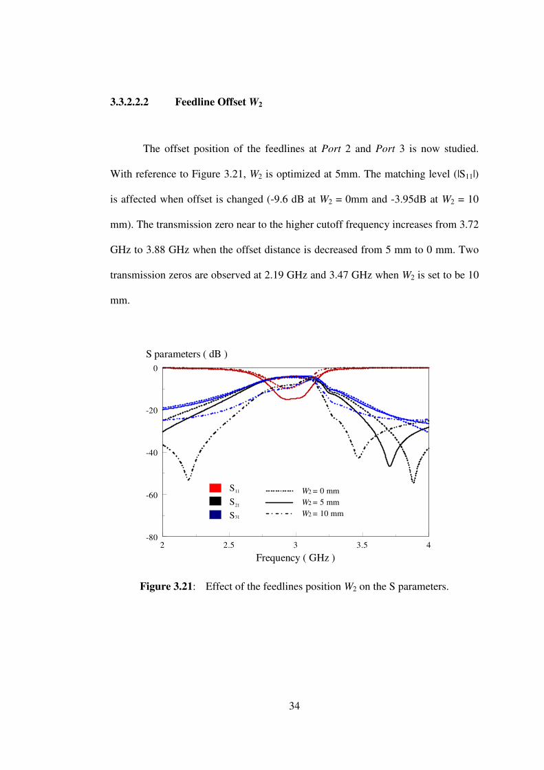
3.3.2.2.2 Feedline Offset W2 34
3.3.2.2.3 Length of Patch L1 35
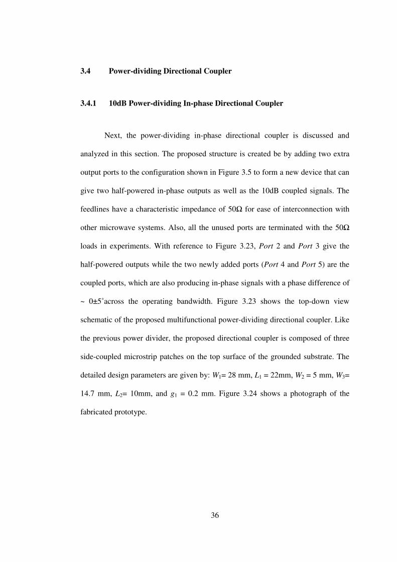
3.4 Power-dividing Directional Coupler 36
3.4.1 10 dB Power-dividing In-phase Directional Coupler 36
3.4.1.1 Simulation and Experiment Results 38
3.4.2 10 dB Power-dividing Out-of-phase Directional Coupler 42
3.4.2.1 Simulation and Experiment Results 43
3.4.3 20 dB Power-dividing Directional Coupler 47
3.4.3.1 Simulation and Experiment Results 48
3.5 Multifunctional Directional Coupler with Multiple Outputs 53
3.5.1 Simulation and Experimental Results 54
3.6 Conclusion 58
4 STEPPED-IMPEDANCE SLOTLINE POWER DIVIDERS 59
4.1 Introduction 59
4.2 Design Methodology 61
4.3 In-phase Power Divider 65
4.3.1 Configuration 65

ix
4.3.2 Simulation and Experiment Results 66
4.3.3 Theoretical and Parametric Studies 69
4.3.3.1 Slot Length L1 70
4.3.3.2 Slot Width W1 71
4.3.3.3 Slotline Length d1 72
4.3.3.4 Slotline Length d4 73
4.3.3.5 Slotline Widths b1 and b4 74
4.3.3.6 Stripline Length l2 and l3 75
4.4 Out-of-Phase Power Divider 77
4.4.1 Configuration 77
4.4.2 Simulation and Experiment Results 78
4.4.3 Theoretical and Parametric Studies 81
4.4.3.1 Slot Length L1 82
4.4.3.2 Slot Width W1 83
4.4.3.3 Slotline Length d1 84
4.4.3.4 Slotline Length d4 85
4.4.3.5 Stripline Length l2 and l3 86
4.5 Reconfigurable Power Divider 88
4.5.1 Configuration 88
4.5.2 Biasing Circuitry for RF PIN Diode 90
4.5.3 Simulation and Experimental Results 91
4.6 Conclusion 94
5 CONCLUSION 96
5.1 Conclusion 96
5.2 Future Works 96
Bibliography
References

x
LIST OF TABLES
TABLE TITLE PAGE
Table 3.1: Transmission zeros near to the lower and higher cut-off frequencies. 55

xi
LIST OF FIGURES
FIGURE TITLE PAGE
Figure 2.1: The schematic of a conventional power divider. 6
Figure 2.2: The schematic of a conventional directional coupler. 7
Figure 3.1: (a) Configuration of a rectangular microstrip patch, (b) Electric field distribution at 2.9 GHz. 16
Figure 3.2: Simulated S parameters of the simple rectangular patch shown in Figure 3.1(a). 17
Figure 3.3: Simulated S parameters of the new patch structure (in the inset) with two additional side patches. 17
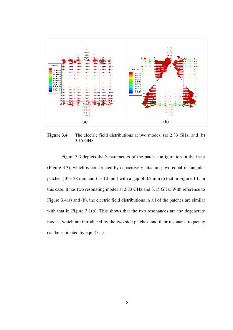
Figure 3.4: The electric field distributions at two modes, (a) 2.83 GHz, and (b) 3.15 GHz. 18
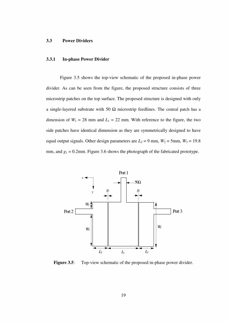
Figure 3.5: Top-view schematic of the proposed in-phase power divider. 19
Figure 3.6: Prototype of the proposed in-phase power divider. 20
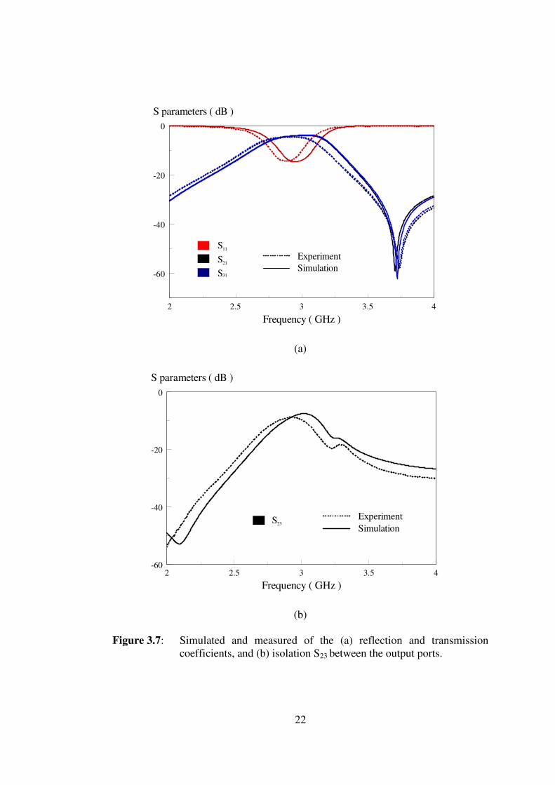
Figure 3.7: Simulated and measured of the (a) reflection and transmission coefficients, and (b) isolation S23 between the output ports. 22
Figure 3.8: Simulated and measured of the group delay of the proposed in-phase power divider. 23
Figure 3.9: Calculated amplitude imbalance and phase difference. 23
Figure 3.10: The electric field distributions of the proposed in-phase power divider at poles, (a) 2.828 GHz, and (b) 3.081 GHz. 24
Figure 3.11: Effect of patch width W1 on the S parameters. 25
xii
Figure 3.12: Effect of the feedline position W2 on the S parameters. 26
Figure 3.13: Effect of gap distance g1 between patches on the S parameters. 27
Figure 3.14: Top-view schematic of the proposed out-of-phase power divider. 28
Figure 3.15: Prototype of the proposed out-of-phase power divider. 29
Figure 3.16: Simulated and measured (a) reflection and transmission coefficients, and (b) isolation S23 between the output ports. 30
Figure 3.17: Simulated and measured group delay. 31
Figure 3.18: Calculated amplitude imbalance and phase difference. 31
Figure 3.19: The electric field distributions of the proposed out-of-phase power divider at poles, (a) 2.82 GHz, and (b) 3.11 GHz. 32
Figure 3.20: Effect of the patch widthW1on the S parameters. 33
Figure 3.21: Effect of the feedlines positionW2on the S parameters. 34
Figure 3.22: Effect of the patch length L1 on the S parameters. 35
Figure 3.23: Top-view schematic of the proposed 10 dB power-dividing in-phase directional coupler. 37
Figure 3.24: Prototype of the proposed 10 dB power-dividing in-phase directional coupler. 37
Figure 3.25: Simulated and measured (a) reflection and transmission coefficients, and (b) isolation levels between the output ports. 39
Figure 3.26: Calculated amplitude imbalance and phase difference of the (a) half-powered outputs, and (b) 10 dB coupled ports. 40
Figure 3.27: Simulated and measured group delays for the (a) half-powered outputs, and (b) 10 dB coupled ports. 41

xiii
Figure 3.28: Top-view schematic of the proposed 10 dB power-dividing out-of-phase directional coupler. 42
Figure 3.29: Prototype of the proposed 10 dB power-dividing out-of-phase directional coupler. 43
Figure 3.30: Simulated and measured (a) reflection and transmission coefficients, and (b) isolation levels between the output ports. 44
Figure 3.31: Calculated amplitude imbalance of the (a) half-powered outputs, and (b) 10 dB coupled ports. 45
Figure 3.32: Simulated and measured group delays of the (a) half-powered outputs, and (b) 10 dB coupled ports. 46
Figure 3.33: Top-view schematic of the proposed 20 dB power-dividing directional coupler. 47
Figure 3.34: Prototype of the proposed 20dB power-dividing directional coupler. 48
Figure 3.35: Simulated and measured (a) reflection and transmission coefficients, and (b) isolation levels between the output ports 50
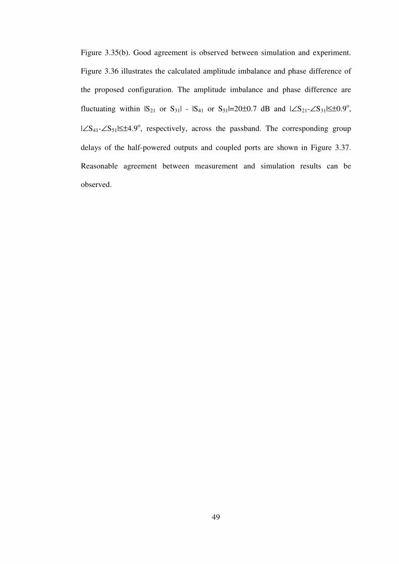
Figure 3.36: Calculated amplitude imbalance of the (a) half-powered outputs, and (b) 20 dB coupled ports. 51
Figure 3.37: Simulated and measured group delays of the (a) half-powered outputs, and (b) 20 dB coupled ports. 52
Figure 3.38: Schematic of the proposed multifunctional directional coupler with multiple outputs. 53
Figure 3.39: Prototype of the proposed multifunctional directional coupler. 54
Figure 3.40: Simulated and measured S parameters. 56
Figure 3.41: Simulated and measured isolation levels between the output ports. 56
Figure 3.42: Calculated amplitude imbalance and phase difference. 57
Figure 3.43: Measured and simulated group delays. 57

xiv
Figure 4.1: (a) The configuration of the stepped-impedance slot with a hook-shaped feedline, (b) Simulated S parameters of the configuration in Figure 4.1(a) with different width values. 62
Figure 4.2: The electric field distributions for different W values at the two modes, (a) 0.6 mm, (b) 8 mm, and (c) 16 mm. 64
Figure 4.3: Top-view schematic of the proposed in-phase power divider. 65
Figure 4.4: Prototype of the proposed in-phase power divider, (a) Top View, (b) Bottom View. 66
Figure 4.5: Simulated and measured (a) reflection and transmission coefficients, and (b) isolation level between the output ports. 67
Figure 4.6: Calculated amplitude imbalance and phase difference. 68
Figure 4.7: Simulated and measured group delays. 68
Figure 4.8: The electric field distributions of the proposed in-phase power divider at (a) the first pole at 4.16 GHz, (b) the second pole at 4.88 GHz, 69
Figure 4.9: Effects of the slot length L1 on the S parameters. 70
Figure 4.10: Effect of the slot width W1 on the S parameters. 71
Figure 4.11: Effect of the slotline length d1 on the S parameters. 72
Figure 4.12: Effect of the slotline length d4 on the S parameters. 73
Figure 4.13: Effect of the slotline width b1 on the S parameters. 74
Figure 4.14: Effect of the slotline width b4 on the S parameters. 75
Figure 4.15: Effect of the stripline length l2 on the S parameters. 76
Figure 4.16: Effect of the stripline length l3 on the S parameters. 76

xv
Figure 4.17: Top-view schematic of the proposed out-of-phase power divider. 77
Figure 4.18: Prototype of the proposed out-of-phase power divider, (a) Top View, (b) Bottom View. 78
Figure 4.19: Simulated and measured (a) reflection and transmission coefficients, and (b) isolation level between the output ports. 79
Figure 4.20: Calculated amplitude imbalance and phase difference. 80
Figure 4.21: Simulated and measured group delays. 80
Figure 4.22: The electric field distributions of the proposed out-of-phase power divider at the poles at (a) 4.14 GHz, and (b) 4.57 GHz. 81
Figure 4.23: Effect of the slot length L1 on the S parameters. 82
Figure 4.24: Effect of the slot width W1 on the S parameters. 83
Figure 4.25: Effect of the slotline length d1 on the S parameters. 84
Figure 4.26: Effect of the slotline length d4 on the S parameters. 85
Figure 4.27: Effect of the stripline length l2 on the S parameters. 86
Figure 4.28: Effect of the stripline length l3 on the S parameters. 87
Figure 4.29: Schematic of the proposed reconfigurable power divider. 89
Figure 4.30: Prototype of the proposed reconfigurable power divider, (a) Top View, (b) Bottom View. 89
Figure 4.31: Biasing Circuitry for the RF PIN Diode. 90
Figure 4.32: Simulated and measured S parameters of the reconfigurable in-phase power divider (with Port
2 OFF but others ON). 92
xvi
Figure 4.33: Calculated amplitude imbalance and phase difference of the reconfigurable in-phase power divider (with Port 2 OFF but others ON). 92
Figure 4.34: Simulated and measured S parameters of the reconfigurable out-of-phase power divider (with Port 3 OFF but others ON). 93
Figure 4.35: Calculated amplitude imbalance and phase difference of the reconfigurable out-of-phase power divider (with Port 3 OFF but others ON). 94

CHAPTER 1
INTRODUCTION
1.1 Background
Microwave is defined as an electromagnetic wave with frequency ranging
from 300 MHz to 300 GHz, which corresponds to wavelengths from 1 m to 1 mm
in free space. Signals with wavelength less than 1 mm are often referred to as
millimeter waves (D. M. Pozar, 2011). Most of the microwave technologies are
intended for the wireless networking and communication systems. Nowadays, with
the rapid growth of the mobile and wireless communications, microwave
components are highly sought after. In this thesis, several microwave power
dividers and directional couplers will be studied. The background of the
components will be briefly introduced here.
In the past, many types of microwave resonators were proposed for
designing various power-dividing structures (E. J. Wilkinson, 1960; M. E. Goldfarb,
1991; M. Nakatsugawa, K. Nishikawa, 2001). Among all, the Wilkinson power
divider, which makes use of the quarter-wavelength microstrip lines, is the most
popular as it has low coupling between the output ports. Later, many other power
dividers have been proposed by modifying the Wilkinson in order to achieve
different purposes such as dual-band operation (Y. Wu, Y. Liu, et al., 2011; B. Li,
X. Wu, et al., 2011; A. S. S. Mohra, 2008), tri-band operation (H. Chen, Y. Pang,

2
2011; X. Wang, Y. Bai, et al., 2011; B. Li, X. Wu, et al., 2011), ultra wideband
operation (X. Ou, Q. Chu, 2008; D. Hawatmeh, N. Dib, et al., 2012), good
harmonic suppression (K. Yi, B. Kang., 2003; J. Wang, J. Ni, et al., 2009; D. Woo,
T. Lee, 2005), as well as high isolation with an improved bandwidth (J. Kao, Z.
Tsai, et al., 2012) etc.
In the 40s, several directional couplers were invented and characterized at
the MIT Radiation Laboratory (D. M. Pozar, 2011). These include the Bethe-hole
coupler, the multi-hole directional coupler, and others which are designed using the
coaxial lines. In the mid-50s to 60s, many of these directional couplers were re-
designed using the stripline and microstrip technologies because they are planar
and easy to integrate with other microwave systems. Again, bandwidth expansion is
a current heat. A wideband composite right/left-handed (CRLH) coplanar
waveguide (CPW) coupler, with 3dB coupling value and quadrature phase
difference, was proposed by (S. Mao, M. Wu, 2007). The authors have made use of
the symmetrical structure, consisting of a gap capacitor, a broadside-coupled
capacitor, and a meandering short-circuited stub inductor, to achieve wide
operating bandwidth. Microstrip and suspended stripline were combined to design a
directional coupler with wide bandwidth and low insertion loss (S. Lin, M. Eron, et
al., 2011).

3
1.2 Research Objectives and Motivation
This thesis encompassed two design projects. The main objective here is to
explore the multifunction of the multiport microstrip resonator as either a passive
or an active device. In the first part, degenerate modes are deployed to design the
multifunctional and multiport power-dividing directional couplers in a microstrip
rectangular patch resonator. It is able to provide half-power division as well as the
10 dB and 20 dB coupling outputs at the same time. Next, several multiport
microstrip power dividers, which are designed using the stepped-impedance
slotline on a ground plane, are proposed. They can provide in-phase or out-of-phase
operation in a single module.
1.3 Thesis Organization
Chapters 1 and 2 briefly introduce the background of the microwave power
dividers and directional couplers. The recent developments and applications of the
two components are analyzed, along with the research objectives and motivation.
Some technologies that are used to achieve broad bandwidth, multifunction, and
miniaturization are discussed.
In Chapter 3, several directional couplers are proposed and discussed. It
starts with the discussion of the passive in-phase and out-of-phase power dividers.
4
Then, the two are combined to form the 10dB and 20dB power-dividing directional
couplers. Lastly, a multifunctional power-dividing directional coupler that can
produce outputs with multiple levels is demonstrated. Measured and simulated
insertion losses, reflection coefficients, amplitude imbalances, and phase
differences, and group delays are presented, showing good agreement.
Chapter 4 proposes the stepped-impedance slotline power-dividing
structures. To begin, the passive in-phase and out-of-phase power dividers are
studied. By incorporating a few RF PIN diodes, the two are combined to form a
reconfigurable unit. Again, the insertion losses, reflection coefficients, phase
differences, and group delays are investigated. Finally, the design parameters are
studied.
Chapter 5 summarizes the research works presented in this thesis.

5
CHAPTER 2
LITERATURE REVIEW ON MICROWAVE COUPLER
2.1 Background and Introduction
Microstrip couplers are passive microwave components that have been
widely used in microwave applications such as antenna feeds, power amplifiers,
mixers and others. Couplers can be divided into two categories, first for equal
(power divider) power division while second for unequal (directional coupler).
Both of these components can perform power division or combining. Recently,
most of the microstrip couplers (A. M. Abbosh, M. E. Bialkowski, 2007; N. Yang,
C. Caloz, et al., 2010; M. E. Bialkowski, Y. Wang, 2010; C. Lin, S. Chung, 2011)
are made multifunctional in order to achieve compact size and low cost.
Furthermore, new technologies are also employed to achieve wide passband, good
isolation between the output ports as well as high harmonic suppression. Recent
development will be discussed for power dividers and directional couplers in the
following sections.
6
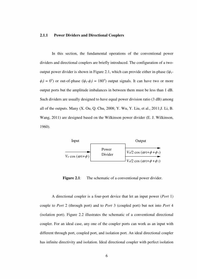
2.1.1 Power Dividers and Directional Couplers
In this section, the fundamental operations of the conventional power
dividers and directional couplers are briefly introduced. The configuration of a two-
output power divider is shown in Figure 2.1, which can provide either in-phase (|ϕ1-
ϕ2| = 0o) or out-of-phase (|ϕ1-ϕ2| = 180o) output signals. It can have two or more
output ports but the amplitude imbalances in between them must be less than 1 dB.
Such dividers are usually designed to have equal power division ratio (3 dB) among
all of the outputs. Many (X. Ou, Q. Chu, 2008; Y. Wu, Y. Liu, et al., 2011;J. Li, B.
Wang, 2011) are designed based on the Wilkinson power divider (E. J. Wilkinson,
1960).
Figure 2.1: The schematic of a conventional power divider.
A directional coupler is a four-port device that let an input power (Port 1)
couple to Port 2 (through port) and to Port 3 (coupled port) but not into Port 4
(isolation port). Figure 2.2 illustrates the schematic of a conventional directional
coupler. For an ideal case, any one of the coupler ports can work as an input with
different through port, coupled port, and isolation port. An ideal directional coupler
has infinite directivity and isolation. Ideal directional coupler with perfect isolation
Power
Divider
Output
Vo cos (ω t+φ )Vo/2 cos (ω t+φ +φ 1)
Vo/2 cos (ω t+φ +φ 2)
Input

7
and matching performances can be realized only if the resonator structure is
symmetric (M. Dydyk, 1999).
Figure 2.2: The schematic of a conventional directional coupler.
2.1.2 Microwave Resonators
Microwave resonator is used by many applications such as oscillators,
mixers, and others. A microwave resonator operates in the way very similar to
those made of lumped-elements (D. M. Pozar, 2011). There are several types of
microwave resonators such as patch resonators (S. R. Zinka, A. Moham, et al.,
2007; J. Xiao, Q. Chu, et al., 2008; J. Li, J. Wang, et al., 2010; R. Zhang, L. Zhu, et
al., 2012), slot resonators (A. A. Semenov, P. Yu, et al., 2008; M. Ohira, Z. Ma, et
al., 2011; Y. Lu, S. Chen, et al., 2012; C. Lee, C. G. Hsu, et al., 2012), and
dielectric resonators (R. Zhang, R. R. Mansour, 2007; A. A. Kishk, W. Huang,
2011; A. Bhardwaj, V. D. Kumar, 2012; K. A. O’Connor, R. D. Curry, 2012). All
have been widely used to design various microwave components. Patch resonator is
planar but with a higher conduction loss. Having a low Q factor, the slot resonator
is able to provide broad bandwidth. But this comes with poorer frequency
Input Through
Isolation Coupled
Directional
Coupler
1 2
34

8
selectivity. To improve it, the dielectric resonator (DR) can be deployed as it has a
higher Q factor.
Power dividers made by slot resonators are popular. In (A. Dadgarpour, G.
Dadashzadeh, et al.; 2010), a compact planar UWB in-phase power divider is
proposed by joining up three T-shaped microstrip lines in parallel on the top
surface of substrate with a H-shaped slot etched on the reverse. The authors in (M.
E. Bialkowski, A. M. Abbosh; 2007) employed a T-junction formed by a slotline
and a microstrip line to design a compact out-of-phase planar power divider. Later,
a similar structure was also proposed by (H. Ma, Q. Chu, et al.; 2008) using a T-
shaped microstrip-etched slot to achieve equal power division with high phase
stability. Slot resonators can also incorporate multilayered technologies for
designing various high-performing power dividers. In (K. Song, Y. Fan, et al.;
2008), a wideband power divider is designed with the use of a five-layered
broadside slot-coupled configuration. Another piece of work, (Q. Li, J. Gong, et al.;
2010) proposed a broadband in-phase structure that was achieved by combining the
elliptical microstrip patches with a rectangular slot.

9
2.2 Recent Developments of Power Dividers
2.2.1 Broadband and Dualband Power Dividers
The demand on various wideband power-dividing structures is on the rise
because of the emergence of myriads of broadband wireless systems. To extend the
frequency passband of a power divider, multiple resonances are usually required. In
(W. Liu, F. Wei, et al., 2012), a novel microstrip power divider is proposed by
installing three open stubs and two aperture-backed interdigital coupled-lines to
excite a couple of resonances, providing ultrawide bandwidth as well as good
impedance matching at all of the output ports. Another broadband power divider
with good in-band power splitting is proposed in (S. W. Wong, L. Zhu, 2008) by
cascading a pair of stepped-impedance open-circuited stubs and parallel-coupled
lines, again, for the excitation of multimode. To do this, multistage λ/4 impedance
transformers can also be introduced (F. Xu, G. Guo, et al., 2012; Y. Wu, X. Xie, et
al., 2012) to broaden the passband. Multiple frequency channels are strongly
needed by the communication systems. Many dual- and multi-band circuits have
been proposed to meet this demand. It was found in (X. Li, Y. J. Yang, et al., 2009)
that open and short stubs can be used to produce double passbands. Similar
technique was also demonstrated by (J. Lee, I. Jeon, et al., 2012).

10
2.2.2 Multifunctional Power Dividers
Recently, the multifunction concept has been explored for miniaturizing
many microwave components (E. H. Lim, K. W. Leung; 2012). It is a trend to
make a power divider to provide output signals with different phases in a single
piece. In (M. E. Bialkowski, Y. Wang, 2011), the authors have used the microstrip-
slot technology to design a Wilkinson power divider that can generate in-phase and
out-of-phase (180o) outputs. Similar technology was again demonstrated by the
same authors in (M. E. Bialkowski, Y. Wang, 2010).
Most of the standalone microwave power dividers do not have filtering
effect. To improve their frequency selectivity, they are usually cascaded with
bandpass filters. This is not desirable as it makes the component bulky. Recently, it
has seen the formation of the concept of filtering power divider, which is a
multifunctional device that can provide half-powered division as well as remove
unwanted signals. Integration of a single-stage coupled line bandpass filter and a
conventional Wilkinson power divider was proposed in (P.K. Singh, S. Basu, et al.,
2009) to achieve filtering effect. Also, bandpass-filtering response was introduced
into the power-dividing structure by using the multilayer microstrip line-slotline
coupling structure (K. Song, Q. Xue, 2010). Later, (M. A. Beldi, F. Boone, et al.,
2012) showed that filtering effect was also possible by combining several T-
junctions into the power divider.

11
2.3 Recent Developments of Directional Couplers
2.3.1 Broadband Directional Couplers
Broadband directional couplers are a very important category of passive
microwave circuits which are used for power dividing/combining, sampling, signal
rejection and power monitoring in microwave communication sub-systems. Some
of the recent technologies are introduced here. A double-layer and multi-aperture
directional coupler was presented in (C. Wang, K. Chang, 2002). It consists of two
back-to-back substrates along with 15 small coupling apertures on the central
ground plane to greatly increase the operating bandwidth. A broadband 8.34 dB
directional coupler was proposed by (S. Gruszczynski, K. Wincza, 2007) using a
stripline technique, where a three-section asymmetric coupled-line was used to
achieve broadband frequency response. (M. E. Bialkowski, N. Seman, et al., 2009)
has proposed a compact ultra-wideband 3 dB directional coupler which consists of
two elliptically shaped conducting disks. A low profile broadband directional
coupler was demonstrated by combining the microstrip line and the suspended
stripline, giving low insertion loss and high power capability in (S. Lin, M. Eron, et
al., 2011).

12
2.3.2 Miniaturized Directional Couplers
Nowadays, increasing attention has been paid to researching various
miniaturized microwave components to achieve compact size. By introducing
different equivalent inductances for the even and odd modes, (J. Yen, S. Hsu, et al.,
2011) showed that the circuit size of a forward-wave directional coupler can be
much reduced. The same group of researchers also proposed another
miniaturization method by introducing the periodical mushroom-shaped ground
plane to the conventional coupled-line directional coupler, which has identical
characteristic impedances for the even and odd modes (S. Hsu, C. Tsai, et al., 2010).
Besides that, the defected ground structure described in (J. Yen, S. Hsu, et al., 2011)
can be used to make a directional coupler compact. In (P. Chi, T. Itoh, 2009), the
authors designed a compact dual-band directional coupler using the composite
right/left-handed (CRLH) transmission structures.

13
CHAPTER 3
MULTIFUNCTIONAL POWER-DIVIDING DIRECTIONAL COUPLERS
WITH MULTIPLE OUTPUTS
3.1 Introduction
Couplers are widely used in microwave applications such as mixers, phase
shifters and antenna arrays. Branch-line (J. Reed, G. J. Wheeler; 1956) was used
for providing equal power division and 90o phase shift, but it has a bandwidth (BW)
of ~10% only. Although the BW can be broadened by cascading multiple branch
lines, it introduces additional coupling between the branches and such structure has
very high impedance lines that are difficult to be made. Also, the junctions
introduce parasitic reactances. In order to overcome these problems, patch coupler
was introduced. In 1980s, a simple 3dB rectangular patch coupler was proposed in
(J. W. Burn; 1985; V.F. Fusco, J.A.C. Stewart, 1986; V. F. Fusco, L. N. Merugu;
1990). The design equation was given in (J. W. Burn; 1985) for calculating the
resonance frequency of the rectangular microstrip patch coupler. Patch couplers can
be easily designed into different shapes such as rectangular, circular (K. C. Gupta,
M. Abouzahra, 1985; M. Abouzahra, K. C. Gupta, 1987), and elliptical (M. E.
Bialkowski, S. T. Jellett, 1994; K. L. Chan, F. A. Alhargan, et al.; 1997). Open-
/shorted stubs and impedance steps are introduced to the periphery of the microstrip
resonators (T. Kawai, I. Ohta,et al; 1992; M. E. Bialkowski, S. T. Jellett; 1994) to
obtain flat coupling response and broader operational bandwidth. Without using
any stub, Chan etal. (K. L. Chan, F. A. Alhargan, et al.; 1997) showed that the

14
quadrature bandwidth of an elliptical patch hybrid can also be improved by
inserting impedance transformers into the feedlines. Recently, various methods
have been proposed to miniaturize the conventional patch hybrid coupler.
Asymmetrically loaded cross slots (S. Sun, L. Zhu, 2009) are added to the
conventional 3dB patch hybrid to reduce the overall size due to its inductive
loading effect. In (S. Y. Zheng, S. H. Yeung, et al., 2009), the size of patch hybrid
is miniaturized by introducing patternedslots behind the patch resonator without
increasing circuit complexity.
In modern microwave systems, integration of multiple RF components into
a single module has been widely used in order to obtain multi-functionality such as
high compactness, low loss, and low cost (E. H. Lim, K. W. Leung, 2012).
Recently, patch resonator has also been explored for multifunction. Two cross-
slotted patch resonators with an inserted conductor plane (J. X. Chen, C. Y. Cheung,
et al., 2007) are sandwiched to make a dual-mode balun bandpass filter. However,
the additional conductor plane increases the material cost and design complexity. In
order to solve this problem, a dual-mode balun filter with only a single cross-
slotted patch resonatorwas proposed (S. Sun, W. Menzel, 2011; C. H. Ng, E. H.
Lim, et al., 2011), where two degenerate modes are excited by the etched
asymmetrical-cross slots. So far, the dualfunction of the patch as a power divider
and a directional coupler has not been found.
In this chapter, a microstrip patch is explored for designing six different
power-dividing structures. In the first part, the patch is dividing an input power into
two outputs, which can be made to be either in-phase or out-of-phase. By adding in

15
two extra output ports, the proposed patch can function simultaneously as 10dB and
20dB power-dividing directional couplers. Here, the 10dB coupled signals can be
made either in- or out-of-phase. It is very interesting to note that the proposed
configuration can provide half-power, as well as 10dB and 20dB couplings at the
same time. All the simulated results are accomplished using Ansoft HFSS (Ansoft
Corporation, HFSS). Experiment was conducted on the R&S®ZVB8 Vector
Network Analyzer (VNA). The substrate Duroid RO4003C, with a dielectric
constant of εr = 3.38 and a thickness of h = 1.524 mm, was used throughout the
entire project. In this chapter, the design methodology, configurations, results,
discussions, and parametric analysis of the proposed multifunctional couplers are
presented.
3.2 Design Methodology
In this section, the design methodology will be discussed and analyzed.
Figure 3.1(a) shows the configuration of a rectangular microstrip patch, with its
electric field distribution depicted in Figure 3.1(b) for the TE01 mode. It has one
null in the y-direction. The resonant frequency of the TEnm mode can be calculated
by using the cavity model describable by eqn. (3.1), where n and m denote the
numbers of nulls in the x- and y- directions. Here, c is the speed of light and εr is
the relative permittivity of substrate. This model holds when the substrate thickness
(h) is small, where electric field (Ez) variation in the z-direction is assumed to be
constant due to negligible substrate thickness.
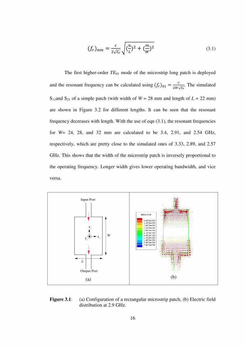
16
() = √ (
) + () (3.1)
The first higher-order TE01 mode of the microstrip long patch is deployed
and the resonant frequency can be calculated using() = √. The simulated
S11and S21 of a simple patch (with width of W = 28 mm and length of L = 22 mm)
are shown in Figure 3.2 for different lengths. It can be seen that the resonant
frequency decreases with length. With the use of eqn (3.1), the resonant frequencies
for W= 24, 28, and 32 mm are calculated to be 3.4, 2.91, and 2.54 GHz,
respectively, which are pretty close to the simulated ones of 3.33, 2.89, and 2.57
GHz. This shows that the width of the microstrip patch is inversely proportional to
the operating frequency. Longer width gives lower operating bandwidth, and vice
versa.
(a)
(b)
Figure 3.1: (a) Configuration of a rectangular microstrip patch, (b) Electric field distribution at 2.9 GHz.
Output Port
Input Port
W
L
kx
k y
kz

17
Figure 3.2: Simulated S parameters of the simple rectangular patch shown in
Figure 3.1(a).
Figure 3.3: Simulated S parameters of the new patch structure (in the inset) with two additional side patches.
2 2.5 3 3.5 4
-40
-30
-20
-10
0
Frequency ( GHz )
S parameters ( dB )
S11
S21
W1 = 28 mm
W1 = 24 mm
W1 = 32 mm
2 2.5 3 3.5 4-60
-40
-20
0
Frequency ( GHz )
S parameters ( dB )
S11S21
Additional patches
W
L
18
(a)
(b)
Figure 3.4: The electric field distributions at two modes, (a) 2.83 GHz, and (b) 3.15 GHz.
Figure 3.3 depicts the S parameters of the patch configuration in the inset
(Figure 3.3), which is constructed by capacitively attaching two equal rectangular
patches (W = 28 mm and L = 10 mm) with a gap of 0.2 mm to that in Figure 3.1. In
this case, it has two resonating modes at 2.83 GHz and 3.15 GHz. With reference to
Figure 3.4(a) and (b), the electric field distributions in all of the patches are similar
with that in Figure 3.1(b). This shows that the two resonances are the degenerate
modes, which are introduced by the two side patches, and their resonant frequency
can be estimated by eqn. (3.1).
19
3.3 Power Dividers
3.3.1 In-phase Power Divider
Figure 3.5 shows the top-view schematic of the proposed in-phase power
divider. As can be seen from the figure, the proposed structure consists of three
microstrip patches on the top surface. The proposed structure is designed with only
a single-layered substrate with 50 Ω microstrip feedlines. The central patch has a
dimension of W1 = 28 mm and L1 = 22 mm. With reference to the figure, the two
side patches have identical dimension as they are symmetrically designed to have
equal output signals. Other design parameters are L2 = 9 mm, W2 = 5mm, W3 = 19.8
mm, and g1 = 0.2mm. Figure 3.6 shows the photograph of the fabricated prototype.
Figure 3.5: Top-view schematic of the proposed in-phase power divider.
Port 1
Port 2 Port 3
y
x
L1L2 L2
W1
W2
W3
g1g1
50Ω

20
Figure 3.6: Prototype of the proposed in-phase power divider.
3.3.1.1 Simulation and Experimental Results
Figure 3.7(a) shows the simulation and measurement results of the proposed
power divider in Figure 3.5. The proposed structure has a measured passband
covering frequencies from 2.77 GHz to 3.0 GHz, giving a fractional bandwidth
(FBW) of 8.15% (simulation: 2.83 GHz – 3.08 GHz, FBW: 8.53%). In the
passband, the measured insertion loss is in the range of -4.5dB to -5.3dB
(simulation: -3.8dB - -4.7dB). Because of its conduction loss, the patch resonator
usually has higher insertion loss (C. Pedro, T. S. Lv, et al., 2011; S. Sun, W.
Menzel; 2011). Additional loss can be introduced by impedance mismatch between
the feedlines and connectors in experiment. Both of the simulated and measured
|S11| read ~ -15 dB. The measured and simulated center frequencies are 2.89 GHz
and 2.96 GHz, respectively, with an error of 2.42%.There is a transmission zero at
2.72 GHz. In general, reasonable agreement is observed between simulated and

21
measured results. The isolation level between the two output ports is illustrated in
Figure 3.7(b), with measurement going below ~ -9.6 dB across the passband. The
group delay of the proposed structure is shown in Figure 3.8. Reasonable
agreement can be observed. The group delay is almost constant across the passband,
with the measured maximum delay of 1.38 ns (simulation: 1.10 ns). Figure 3.9
shows the measured amplitude imbalance and phase difference of the proposed in-
phase power divider (Figure 3.5). It is observed that the calculated amplitude
imbalance and phase difference are within ± 0.18 dB and 2.3o, respectively, across
the operating bandwidth.
22
(a)
(b)
Figure 3.7: Simulated and measured of the (a) reflection and transmission coefficients, and (b) isolation S23 between the output ports.
2 2.5 3 3.5 4
-60
-40
-20
0
Frequency ( GHz )
S parameters ( dB )
Experiment
Simulation
S11
S21
S31
2 2.5 3 3.5 4-60
-40
-20
0
Frequency ( GHz )
S parameters ( dB )
Experiment
SimulationS23

23
Figure 3.8: Simulated and measured of the group delay of the proposed in-phase power divider.
Figure 3.9: Calculated amplitude imbalance and phase difference.
2.7 2.8 2.9 3 3.10
0.5
1
1.5
2
2.5
Frequency ( GHz )
Delay ( ns )
Experiment
Simulation
S21
S31
2.8 2.9 30
0.2
0.4
0
1
2
3
Frequency ( GHz )
Amplitude Imbalance ( dB ) Phase Difference ( deg )

24
3.3.1.2 Theoretical and Parametric Studies
In this section, the theoretical and parametric studies are analyzed and
discussed. All the simulated results are generated from the configuration in Figure
3.5. The simulated electric field distributions of the poles (P1 = 2.828 and P2 =
3.081 GHz) are shown in vector form in Figure 3.10. With reference to the figure,
the two poles have similar electric field distributions in the central patch but
asymmetrical field patterns at the two side patches. As can be seen from the side
views of Figure 3.10, it is clear that the output signals at the two ports are tapped
symmetrically at two positions which have identical electric vectors, causing them
to have the same phase. To obtain a better understanding, the design parameters of
the in-phase power divider are analyzed.
Top View
Side View
(a)
Top View
Side View
(b)
Figure 3.10: The electric field distributions of the proposed in-phase power divider at poles, (a) 2.828 GHz, and (b) 3.081 GHz.
25
3.3.1.2.1 Widths of Patches W1
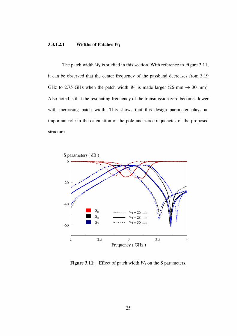
The patch width W1 is studied in this section. With reference to Figure 3.11,
it can be observed that the center frequency of the passband decreases from 3.19
GHz to 2.75 GHz when the patch width W1 is made larger (26 mm → 30 mm).
Also noted is that the resonating frequency of the transmission zero becomes lower
with increasing patch width. This shows that this design parameter plays an
important role in the calculation of the pole and zero frequencies of the proposed
structure.
Figure 3.11: Effect of patch width W1 on the S parameters.
2 2.5 3 3.5 4
-60
-40
-20
0
Frequency ( GHz )
S parameters ( dB )
S11
S21
S31
W1 = 28 mm
W1 = 26 mm
W1 = 30 mm
26
3.3.1.2.2 Feedline Offset W2
Figure 3.12: Effect of the feedline position W2 on the S parameters.
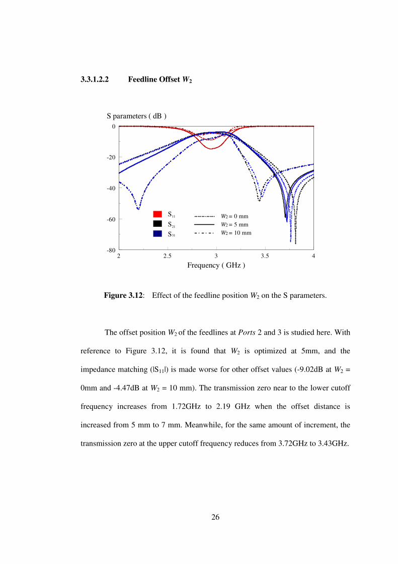
The offset position W2 of the feedlines at Ports 2 and 3 is studied here. With
reference to Figure 3.12, it is found that W2 is optimized at 5mm, and the
impedance matching (|S11|) is made worse for other offset values (-9.02dB at W2 =
0mm and -4.47dB at W2 = 10 mm). The transmission zero near to the lower cutoff
frequency increases from 1.72GHz to 2.19 GHz when the offset distance is
increased from 5 mm to 7 mm. Meanwhile, for the same amount of increment, the
transmission zero at the upper cutoff frequency reduces from 3.72GHz to 3.43GHz.
2 2.5 3 3.5 4-80
-60
-40
-20
0
Frequency ( GHz )
S parameters ( dB )
S11
S21
S31
W2 = 5 mm
W2 = 0 mm
W2 = 10 mm
27
3.3.1.2.3 Gap Distance g1 between Patches
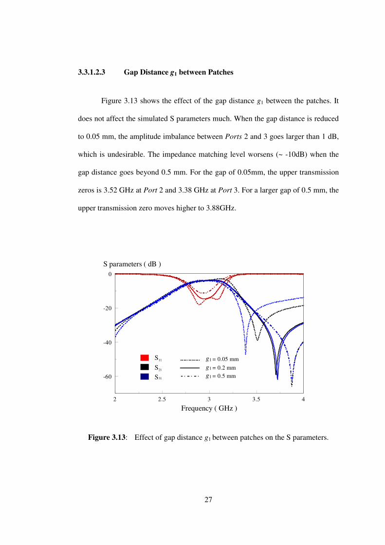
Figure 3.13 shows the effect of the gap distance g1 between the patches. It
does not affect the simulated S parameters much. When the gap distance is reduced
to 0.05 mm, the amplitude imbalance between Ports 2 and 3 goes larger than 1 dB,
which is undesirable. The impedance matching level worsens (~ -10dB) when the
gap distance goes beyond 0.5 mm. For the gap of 0.05mm, the upper transmission
zeros is 3.52 GHz at Port 2 and 3.38 GHz at Port 3. For a larger gap of 0.5 mm, the
upper transmission zero moves higher to 3.88GHz.
Figure 3.13: Effect of gap distance g1 between patches on the S parameters.
2 2.5 3 3.5 4
-60
-40
-20
0
Frequency ( GHz )
S parameters ( dB )
S11
S21
S31
g1 = 0.2 mm
g1 = 0.05 mm
g1 = 0.5 mm

28
3.3.2 Out-of-Phase Power Divider
The configuration of the proposed out-of-phase power divider is shown in
Figure 3.14, which is quite similar to the in-phase one. The only difference is that,
now, the feedline (Port 3) is tapping out signal at the lower end of the side patch. It
will be shown later that this tapping is possible as the side has almost identical field
strength, but with opposite direction, at this position. As can be seen from Figure
3.14, the patch is fed by three 50Ω microstrip feedlines at all of the ports. The
detailed design parameters are given by: W1 = 28 mm, W2 = 5 mm, W3= 19.8 mm,
L1 = 22 mm, L2 = 10 mm, and g1 = 0.2mm. Figure 3.15 shows the photograph of
the fabricated prototype.
Figure 3.14: Top-view schematic of the proposed out-of-phase power divider.
Port 1
Port 2
Port 3
y
x
L1L2 L2
W1
W2
W3
g1g1
W2
50Ω

29
Figure 3.15: Prototype of the proposed out-of-phase power divider.
3.3.2.1 Simulation and Experiment Results
Figure 3.16(a) illustrates the simulation and experimental S parameters of
the proposed out-of-phase power divider. The measured and simulated passbands
are 2.77 – 3.0 GHz and 2.82 – 3.11 GHz, respectively. With the use of
×100% , the measured fractional bandwidth (8.24%) is slight lower than the
simulated (9.51%). In the passband, the measured insertion loss is in the range of -
4.6dB to -5.4dB (simulation: -3.9dB - -4.8dB), with a matching level of ~ -15dB at
the center frequency, which read2.88 GHz in experiment (simulation: 2.97 GHz).
Reasonable agreement was observed between the experimental and simulation
results, with a slight error of 2.82% in the center frequencies. Figure 3.16(b) shows
the isolation between the two output ports. It is lower than -8.5 dB (simulation: -7.2
dB) in measurement. The group delay is shown in Figure 3.17. The group delay is
almost constant across the passband, with the measured maximum delay of 1.41 ns
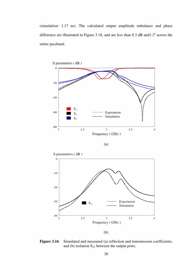
30
(simulation: 1.17 ns). The calculated output amplitude imbalance and phase
difference are illustrated in Figure 3.18, and are less than 0.3 dB and1.3o across the
entire passband.
(a)
(b)
Figure 3.16: Simulated and measured (a) reflection and transmission coefficients, and (b) isolation S23 between the output ports.
2 2.5 3 3.5 4-80
-60
-40
-20
0
Frequency ( GHz )
S parameters ( dB )
Experiment
Simulation
S11
S21
S31
2 2.5 3 3.5 4-40
-30
-20
-10
0
Frequency ( GHz )
S parameters ( dB )
Experiment
SimulationS23

31
Figure 3.17: Simulated and measured group delay.
Figure 3.18: Calculated amplitude imbalance and phase difference.
2.7 2.8 2.9 3 3.10
0.5
1
1.5
2
2.5
Frequency ( GHz )
Delay ( ns )
Experiment
Simulation
S21
S31
2.8 2.9 30
0.2
0.4
178
180
182
Frequency ( GHz )
Amplitude Imbalance ( dB ) Phase Difference ( deg )

32
3.3.2.2 Theoretical and Parametric Studies
In this section, the theoretical and parametric analysis of the proposed out-
of-phase power divider is discussed. Figure 3.19 illustrates the simulated electric
field distributions at pole frequencies, 2.82 GHz and 3.11 GHz. It can be seen from
Figure 3.19 that the field strength at the bottom edge of the side patch maximizes,
with the field in the opposite directions. Referring to the side views in Figure 3.19,
it can be seen that the electric vectors are in the opposite directions at the two
output ports, making the output signals out-of-phase. The design parameters are
also studied here.
Top View
Side View
(a)
Top View
Side View
(b)
Figure 3.19: The electric field distributions of the proposed out-of-phase power divider at poles, (a) 2.82 GHz, and (b) 3.11 GHz.

33
3.3.2.2.1 Widths of Patches W1
Figure 3.20 depicts the simulated S parameters with respect to the change of
the width W1.With reference to the figure, it can be observed that when the patch
width is made smaller (30mm to 26 mm), the centre frequency of the passband
increases from 2.76 GHz to 3.17 GHz. Besides that, the transmission zero shifts to
lower frequency (3.5 GHz) when W1 is increased. This shows that this design
parameter plays an important role in the calculation of the pole and zero
frequencies of the proposed structure.
Figure 3.20: Effect of the patch width W1 on the S parameters.
2 2.5 3 3.5 4
-60
-40
-20
0
Frequency ( GHz )
S parameters ( dB )
S11
S21
S31
W1 = 28 mm
W1 = 26 mm
W1 = 30 mm
34
3.3.2.2.2 Feedline Offset W2
The offset position of the feedlines at Port 2 and Port 3 is now studied.
With reference to Figure 3.21, W2 is optimized at 5mm. The matching level (|S11|)
is affected when offset is changed (-9.6 dB at W2 = 0mm and -3.95dB at W2 = 10
mm). The transmission zero near to the higher cutoff frequency increases from 3.72
GHz to 3.88 GHz when the offset distance is decreased from 5 mm to 0 mm. Two
transmission zeros are observed at 2.19 GHz and 3.47 GHz when W2 is set to be 10
mm.
Figure 3.21: Effect of the feedlines position W2 on the S parameters.
2 2.5 3 3.5 4-80
-60
-40
-20
0
Frequency ( GHz )
S parameters ( dB )
S11
S21
S31
W2 = 5 mm
W2 = 0 mm
W2 = 10 mm

35
3.3.2.2.3 Length of Patch L1
Figure 3.22: Effect of the patch length L1 on the S parameters.
The length of patch L1 is now studied. The simulated S parameters with
respect to the change of L1 are shown in Figure 3.22. The L1 value has only minor
effect on S parameters. With reference to the figure, the optimal value for L1 is 22
mm. Furthermore, no difference is observed in the pole frequencies when the patch
width L1 is varied.
2 2.5 3 3.5 4-60
-40
-20
0
Frequency ( GHz )
S parameters ( dB )
S11
S21
S31
L1 = 22 mm
L1 = 20 mm
L1 = 24 mm
36
3.4 Power-dividing Directional Coupler
3.4.1 10dB Power-dividing In-phase Directional Coupler
Next, the power-dividing in-phase directional coupler is discussed and
analyzed in this section. The proposed structure is created be by adding two extra
output ports to the configuration shown in Figure 3.5 to form a new device that can
give two half-powered in-phase outputs as well as the 10dB coupled signals. The
feedlines have a characteristic impedance of 50Ω for ease of interconnection with
other microwave systems. Also, all the unused ports are terminated with the 50Ω
loads in experiments. With reference to Figure 3.23, Port 2 and Port 3 give the
half-powered outputs while the two newly added ports (Port 4 and Port 5) are the
coupled ports, which are also producing in-phase signals with a phase difference of
~ 0±5˚across the operating bandwidth. Figure 3.23 shows the top-down view
schematic of the proposed multifunctional power-dividing directional coupler. Like
the previous power divider, the proposed directional coupler is composed of three
side-coupled microstrip patches on the top surface of the grounded substrate. The
detailed design parameters are given by: W1= 28 mm, L1 = 22mm, W2 = 5 mm, W3=
14.7 mm, L2= 10mm, and g1 = 0.2 mm. Figure 3.24 shows a photograph of the
fabricated prototype.
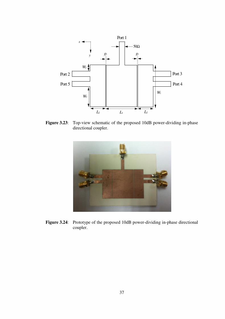
37
Figure 3.23: Top-view schematic of the proposed 10dB power-dividing in-phase
directional coupler.
Figure 3.24: Prototype of the proposed 10dB power-dividing in-phase directional coupler.
Port 1
Port 2 Port 3
y
x
L1L2 L2
W1
W2
W3
g1g1
Port 4Port 5
50Ω

38
3.4.1.1 Simulation and Experimental Results
The simulation and experimental results will be illustrated and analyzed in
this section. Figure 3.25(a) shows the simulated and measured S parameters of the
proposed structure, showing two poles with a measured passband of 2.76 – 3.0
GHz (simulation: 2.84 – 3.09 GHz) and a measured FBW of 8.51%
(simulation:8.33%). In the passband, the measured transmission coefficient is in the
range of -4.9dB to -5.4dB (simulation: -4.3dB - -5.2dB) at Ports 2 and 3, which is
quite close to the theoretical value of -3.98dB. It is lower as part (-10dB) of the
input power has been directed to Ports 4 and 5. The measured and simulated center
frequencies are 2.88 GHz and 2.97 GHz, respectively, with an error of 3.13%. Also,
three transmission zeros are measured at 2.13 GHz (simulation: 2.21 GHz), 3.42
GHz (3.43 GHz), and 3.75 GHz (3.71 GHz). Figure 3.25(b) shows the measured
and simulated coupling coefficients between the output and coupled ports. The
calculated amplitude imbalance and phase difference of the proposed configuration
is illustrated in Figure 3.26. As can be seen from the figure, the amplitude
imbalance and phase difference fall within|S21 or S31|-|S41 or S51|=10±0.3 dB, |∠S21-
∠S31|≤±1o, and|∠S41-∠S51|≤±1.5o, respectively. Both are calculated from the
measured results across the passband. Figure 3.27 shows the measured and
simulated group delays of both of the half-powered output ports and 10dB coupled
ports. Reasonable agreement is observed. It shows that the same piece of resonator
can be used to generate power division and coupling signals. This can lead to
significant cost saving.

39
(a)
(b)
Figure 3.25: Simulated and measured (a) reflection and transmission coefficients, and (b) isolation levels between the output ports.
2 2.5 3 3.5 4
-60
-40
-20
0
Frequency ( GHz )
S parameters ( dB )
S11
S21
S31
S41
S51
Experiment
Simulation
S23
S24
S25
S45
2 2.5 3 3.5 4
-60
-40
-20
0
Frequency ( GHz )
S parameters ( dB )
Experiment
Simulation

40
(a)
(b) Figure 3.26: Calculated amplitude imbalance and phase difference of the (a) half-
powered outputs, and (b) 10dB coupled ports.
2.8 2.9 30
0.2
0.4
0
0.5
1
Frequency ( GHz )
Amplitude Imbalance ( dB ) Phase Difference ( deg )
2.8 2.9 30
0.1
0.2
0.3
0
0.5
1
1.5
2
Frequency ( GHz )
Amplitude Imbalance ( dB ) Phase Difference ( deg )

41
(a)
(b)
Figure 3.27: Simulated and measured group delays for the (a) half-powered outputs, and (b) 10dB coupled ports.
2.7 2.8 2.9 3 3.10
0.5
1
1.5
2
2.5
Frequency ( GHz )
Delay ( ns )
Experiment
Simulation
S21
S31
2.7 2.8 2.9 3 3.10
0.5
1
1.5
2
2.5
Frequency ( GHz )
Delay ( ns )
Experiment
Simulation
S41
S51

42
3.4.2 10dB Power-dividing Out-of-phase Directional Coupler
In this section, the 10dB power-dividing out-of-phase directional coupler is
proposed. It has the same characteristics as the previous one, but provides two half-
powered in-phase output signals (Port 2 and Port 3) as well as another two 180o
out-of-phase coupled outputs (Port 4 and Port 5), which are 10dB lower. Figure
3.28 shows the top-view schematic of the proposed power-dividing out-of-phase
directional coupler, which is quite similar to that in Figure 3.23. The only
difference is that the feedline position for Port 5is further apart from Port 2. This is
because such a feeding configuration can make the signals at Port 4 and Port 5 out-
of-phase. The detailed design parameters are given by: W1 = 28 mm, W2 = 4.9 mm,
W3= 9.9 mm, W4 = 14.7 mm, L1 = 20mm, L2 = 12 mm, and g1 = 0.2 mm. Again, all
the feedlines are designed with a characteristic impedance of 50 Ω. Figure 3.29
shows the top-view photograph of the fabricated prototype.
Figure 3.28: Top-view schematic of the proposed 10dB power-dividing out-of-phase directional coupler.
Port 1
Port 2 Port 3
y
x
L1L2 L2
W1
W2
W3
g1g1
Port 4
Port 5W4
50Ω

43
Figure 3.29: Prototype of the proposed 10dB power-dividing out-of-phase directional coupler.
3.4.2.1 Simulation and Experimental Results
Figure 3.30(a) shows the simulated and measured S parameters of the
proposed structure. Two resonances are observed in the passband. The proposed
structure has a measured passband covering 2.76 – 2.96 GHz (simulation: 2.85 –
3.04 GHz), with a FBW of 7% (simulation: 6.53%). The measured and simulated
center frequencies are 2.86 GHz and 2.95 GHz, respectively, with an error of
2.97%. The simulated and measured coupling coefficients between the output and
coupled ports are shown in Figure 3.30(b). In general, the measured coupling levels
between any two output ports are less than -9.7dB. Good agreement has been
observed between simulation and experimental results. Figure 3.31 illustrates the
calculated amplitude imbalance and phase difference. The amplitude imbalance and
phase difference fall within |S21 or S31| - |S41 or S51|=10±0.8 dB, |∠S21-∠S31|≤±4.5o,
and |∠S41-∠S51|≤180±4o, respectively, in the operating bandwidth. The
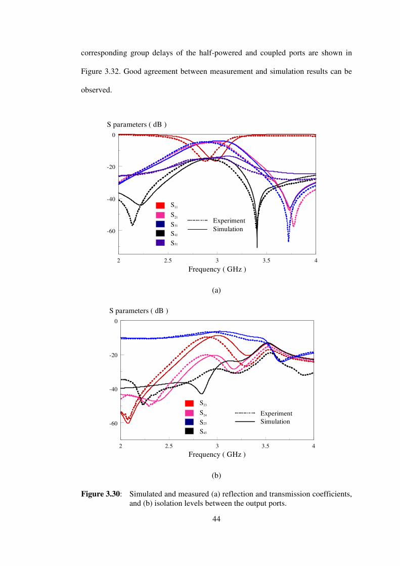
44
corresponding group delays of the half-powered and coupled ports are shown in
Figure 3.32. Good agreement between measurement and simulation results can be
observed.
(a)
(b)
Figure 3.30: Simulated and measured (a) reflection and transmission coefficients, and (b) isolation levels between the output ports.
2 2.5 3 3.5 4
-60
-40
-20
0
Frequency ( GHz )
S parameters ( dB )
S11
S21
S31
S41
S51
Experiment
Simulation
S23
S24
S25
S45
2 2.5 3 3.5 4
-60
-40
-20
0
Frequency ( GHz )
S parameters ( dB )
Experiment
Simulation

45
(a)
(b)
Figure 3.31: Calculated amplitude imbalance of the (a) half-powered outputs, and (b) 10dB coupled ports.
2.8 2.90
0.5
1
0
2
4
Frequency ( GHz )
Amplitude Imbalance ( dB ) Phase Difference ( deg )
2.8 2.90
0.5
1
176
180
184
Frequency ( GHz )
Amplitude Imbalance ( dB ) Phase Difference ( deg )

46
(a)
(b)
Figure 3.32: Simulated and measured group delays of the (a) half-powered outputs, and (b) 10dB coupled ports.
2.7 2.8 2.9 3 3.10
0.5
1
1.5
2
2.5
Frequency ( GHz )
Delay ( ns )
Experiment
Simulation
S21
S31
2.7 2.8 2.9 3 3.10
0.5
1
1.5
2
2.5
Frequency ( GHz )
Delay ( ns )
Experiment
Simulation
S41
S51

47
3.4.3 20dB Power-dividing Directional Coupler
Another new power-dividing directional coupler is proposed in this section.
This time the same configuration is made to generate two in-phase 20dB coupled
signals. To do that, the feeding positions for Port 4 and Port 5 are adjusted along
the edges of the side patches. In this case, the half-powered outputs are also made
to be in-phase. The feedlines are designed with a characteristic impedance of 50 Ω,
with all of the unused ports terminated with 50 Ω loads during measurement. The
top-view schematic of the proposed structure is shown in Figure 3.33. Other design
parameters are given by: W1 = 28 mm, W2 = 5mm, W3 = 13 mm, L1 = 20 mm, L2 =
10 mm, and g1 = 0.2 mm. Figure 3.34 shows the photograph of the fabricated
prototype.
Figure 3.33: Top-view schematic of the proposed 20dB power-dividing directional coupler.
Port 1
Port 2 Port 3
y
x
L1L2 L2
W1
W2
W3
g1g1
Port 4Port 5
50Ω

48
Figure 3.34: Prototype of the proposed 20dB power-dividing directional coupler.
3.4.3.1 Simulation and Experimental Results
The simulated and measured S parameters of the proposed structure are
depicted in Figure 3.35(a). It has a measured passband of 2.77 – 2.99 GHz
(simulation: 2.85 – 3.08 GHz), with a FBW of 7.9% (simulation: 7.58%). The
measured and simulated center frequencies are 2.88 GHz and 2.96 GHz,
respectively, with an error of 2.95%. Transmission zeros are observed in both of
the power division and coupled signals. For the half-power division, a transmission
zero is measured at 3.78 GHz (simulation: 3.74 GHz), very near to the upper cutoff
frequency of the passband. For the coupled signals, very interestingly, one
transmission zero is found near to the lower cutoff frequency (measurement: 2.43
GHz and simulation: 2.55 GHz) while another is observed in the proximity of the
higher one (measurement: 3.27 GHz and simulation: 3.25 GHz). The simulated and
measured coupling coefficients between the output and coupled ports are shown in
49
Figure 3.35(b). Good agreement is observed between simulation and experiment.
Figure 3.36 illustrates the calculated amplitude imbalance and phase difference of
the proposed configuration. The amplitude imbalance and phase difference are
fluctuating within |S21 or S31| - |S41 or S51|=20±0.7 dB and |∠S21-∠S31|≤±0.9o,
|∠S41-∠S51|≤±4.9o, respectively, across the passband. The corresponding group
delays of the half-powered outputs and coupled ports are shown in Figure 3.37.
Reasonable agreement between measurement and simulation results can be
observed.

50
(a)
(b)
Figure 3.35: Simulated and measured (a) reflection and transmission coefficients, and (b) isolation levels between the output ports
2 2.5 3 3.5 4
-80
-60
-40
-20
0
Frequency ( GHz )
S parameters ( dB )
S11
S21
S31
S41
S51
Experiment
Simulation
2 2.5 3 3.5 4
-60
-40
-20
0
Frequency ( GHz )
S parameters ( dB )
Experiment
Simulation
S23
S24
S25
S45
51
(a)
(b)
Figure 3.36: Calculated amplitude imbalance of the (a) half-powered outputs, and (b) 20dB coupled ports.
2.8 2.90
0.2
0.4
0
0.5
1
Frequency ( GHz )
Amplitude Imbalance ( dB ) Phase Difference ( deg )
2.8 2.90
0.2
0.4
0
2
4
Frequency ( GHz )
Amplitude Imbalance ( dB ) Phase Difference ( deg )

52
(a)
(b)
Figure 3.37: Simulated and measured group delays of the (a) half-powered outputs, and (b) 20dB coupled ports.
2.7 2.8 2.9 30
0.5
1
1.5
2
2.5
Frequency ( GHz )
Delay ( ns )
Experiment
Simulation
S21
S31
2.7 2.8 2.9 30
0.5
1
1.5
2
2.5
Frequency ( GHz )
Delay ( ns )
Experiment
Simulation
S41
S51

53
3.5 Multifunctional Directional Coupler with Multiple Outputs
In this section, a multifunctional device that can produce half-power, 10 dB,
and 20dB output signals is proposed. It is interesting to note that the three features
can now be combined into a single module, leading to significant cost saving. The
schematic is depicted in Figure 3.38. In this new design, Port 4 and Port 5 generate
10dB and 20dB coupled output signals, respectively. The detailed design
parameters are given by: W1 = 28 mm, W2 = 5 mm, W3 = 12.9 mm, W4 = 14.7 mm,
L1 = 20 mm, L2 = 10 mm, and g1 = 0.2 mm. The prototype of the proposed structure
is shown in Figure 3.39.
Figure 3.38: Schematic of the proposed multifunctional directional coupler with multiple outputs.
Port 1
Port 2 Port 3
y
x
L1L2 L2
W1
W2
W3
g1g1
Port 4Port 5
W4
50Ω

54
Figure 3.39: Prototype of the proposed multifunctional directional coupler.
3.5.1 Simulation and Experimental Results
In the experiment, all the unused ports were terminated by 50 Ω loads. The
simulated and measured S parameters are shown in Figure 3.40. The measured
passband is 2.8 – 3.0 GHz (simulation: 2.86 – 3.09 GHz) with a FBW of 7.24%
(simulation: 7.72%). The measured center frequency is 2.9 GHz, which is very
close to the simulated one of 2.98 GHz, with an error of 2.67%. Transmission
zeroes, which are found in the transmission coefficients, have been deployed to
sharpen the roll-off of the cutoff skirts of the frequency passbands, as summarized
in Table 3.1.

55
Transmission
Zeros
Zeros near to the lower cut-
off frequency (GHz)
Zeros near to the higher cut-
off frequency (GHz)
Measurement Simulation Measurement Simulation
S21 1.81 1.72 3.83 3.72
S31 1.79 1.72 3.80 3.72
S41 2.14 2.20 3.42 3.45
S51 2.41 2.58 3.35 3.23
Table 3.1: Transmission zeros near to the lower and higher cut-off frequencies.
Figure 3.41 shows the isolation performance between the output ports of the
proposed structure. Good isolation of ~ -10 dB was observed between the output
ports across the passband. The calculated amplitude imbalance and phase
difference are depicted in Figure 3.42. It can be observed that the amplitude
imbalance and phase difference between two half-powered output ports (Port 2 and
Port 3) fall within ≤ 0.74 dB and ±4.3˚, respectively, across the passband. Besides
that, the amplitude difference between the half-power output ports and coupled
ports (Port 4 and Port 5) are around 10±0.9 dB and 20±0.9 dB, respectively. Figure
3.43 illustrates the measured and simulated group delays, and again reasonable
agreement was observed.

56
Figure 3.40: Simulated and measured S parameters.
Figure 3.41: Simulated and measured isolation levels between the output ports.
2 2.5 3 3.5 4
-60
-40
-20
0
Frequency ( GHz )
S parameters ( dB )
S11
S21
S31
S41
S51
Experiment
Simulation
2 2.5 3 3.5 4
-60
-40
-20
0
Frequency ( GHz )
S parameters ( dB )
Experiment
Simulation
S23
S24
S25
S45

57
Figure 3.42: Calculated amplitude imbalance and phase difference.
Figure 3.43: Measured and simulated group delays.
2.8 2.9 30
0.4
0.8
0
2
4
Frequency ( GHz )
Amplitude Imbalance ( dB ) Phase Difference ( deg )
2.8 2.9 30
0.5
1
1.5
2
2.5
Frequency ( GHz )
Delay ( ns )
Experiment
Simulation
S21
S31

58
3.6 Conclusion
In this chapter, several multifunctional power-dividing couplers havebeen
proposed and analyzed. First, the in-phase and out-of-phase power dividers were
demonstrated in Section 3.3.1 and Section 3.3.2. The two proposed power dividers
are made of the same patch resonator, making them to have the same operating
bandwidth. Then, the in-phase one was modified by introducing two additional
coupled ports to form different power-dividing directional couplers, as discussed in
Section 3.4. The multifunctional directional couplers can provide half-powered
output signals as well as the 10dB or 20dB coupled signals at the same time
without affecting the operating passband. The proposed patch coupler can also
accommodate both the10 and 20dB coupled ports simultaneously, which has been
demonstrated in Section 3.5. It is very encouraging to find that a single piece of
resonator can now be used to generate half-powered signals as well as 10dB and
20dB output signals at the same time, making it very versatile. For all the couplers
proposed in this chapter, it has been found that the coupling level of a certain
output feedline can be tuned by adjusting the feeding position along the edge of the
side patch. All the measurement and simulation results show reasonable agreement.

59
CHAPTER 4
STEPPED-IMPEDANCE SLOTLINE POWER DIVIDERS
4.1 Introduction
Microstrip slotline was first proposed in the 1960s (S. B. Cohn; 1968). It is
an alternative to transmission line where a narrow slot or gap is etched on the
conductive layer made on dielectric. Later, (S. B. Cohn; 1969) showed that high-
permittivity substrate can be used to minimize radiation in the slotline. In this case,
the wavelength of the slot mode is much smaller than that for free space, making
fields closely confined around the slot. The characteristics of the microstrip slotline
were analyzed in (E. A. Mariani, C. P. Heinzman, et al., 1969).
Microstrip slotline has been widely introduced to make microwave
components such as antennas (G. Elazar, M. Kisliuk, 1988; H. Iwasaki, K.
Kawabata, 1990; K. Itoh, M. Yamamoto; 1997) and couplers (T. N. Tanaka, K.
Tsunoda, et al., 1988; C. H. Ho, L. Fan, et al., 1993). In (N. Behdad, K. Sarabandi,
2005), it was found that the a second resonance can be excited by feeding a high-
impedance stubline near to the slot edge, combining with the fundamental slot
mode to provide broad bandwidth. The slotline with stepped-impedance shape was
proposed in (X. D. Huang, C. H. Cheng, et al., 2012) to excite four resonant modes,
aiming at achieving ultra-wideband operation. Over the past few years, many
analytical methods have been presented to study the characteristics of the slotline
antenna. A new and wideband transmission line model (J. E. Ruyle, J. T. Bernhard,

60
2011) can be established by using an improved approximation of the voltage,
conductance, and inductance in the slot resonator. This model is able to calculate
the input impedance of the slotline accurately at the higher-order modes. Coupled
slotlines were first introduced by (M. Aikawa, H. Ogawa, 1980) for designing
magic T, where the authors made use of the two orthogonal modes (odd and even)
of this structure to design 180o hybrid. It was recently found that slotline resonator
can also be incorporated with substrate-integrated waveguide (Y. J. Cheng, W.
Hong, et al., 2011) for improving its Q factor.
Multifunctional components have been of great recent interest because of
their various advantages such as providing compact size and low cost. A myriad of
multiple functions have been explored for various couplers. It was shown that a
wideband 180o hybrid, which is able to give in-phase (sigma) and out-of-phase
(delta) wideband outputs the same time, can be designed by using the microstrip-
slot technology (M. E. Bialkowski, A. M. Abbosh,2007; M. E. Bialkowski, Y.
Wang, 2010; M. E. Bialkowski, Y. Wang, 2011). A new 180o hybrid coupler with
dual-bandpass filtering response is proposed in (L. Wu, B. Xia, et al., 2013) by
using four properly designed shorted-stub loaded stepped-impedance resonators,
which are magnetically or electrically coupled among one another.
In this chapter, two passive power dividers with in-phase and out-of-phase
operations have been proposed and investigated. These outputs can be obtained by
tapping out signals at different places along the edge of the slotline resonator. Both
of them can give two resonance modes, very desirable for wideband performance.
Later, the slotline resonator is incorporated with the RF PIN diodes for the design
61
of a multifunctional and reconfigurable power divider. In this case, by switching
ON/OFF the diode, the slotline coupler can produce either an in-phase or out-of-
phase output. All the proposed power dividers are designed with a stepped-
impedance slotline resonator.
Ansoft HFSS is used for conducting all the simulations throughout this
research project. Experimental results are measured by using the R&S®ZVB8
Vector Network Analyzer (VNA). In experiment, all the unused ports were
terminated by 50Ω loads. The substrate has a dielectric constant of εr = 3.38 and a
thickness of h = 1.524 mm. In this chapter, the frequency responses, parametric
analysis, as well as the detailed studies will be performed on the proposed passive
in-phase and out-of-phase power dividers and the reconfigurable power divider.
4.2 Design Methodology
The design methodology will be discussed in this section. Figure 4.1(a)
shows the configuration of a stepped-impedance slot, which is a simplified version
of that in Figure 4.3. It is designed by removing Slotlines 2 and 3 along with their
feeding ports. Other parameters are given by: L = 24 mm, d = 0.6 mm, l1 = 12 mm,
l2 = 15.5 mm, a1 = 9 mm, and a2 = 9.5 mm. It consists of a hook-shaped microstrip
feedline located on the top surface of a grounded substrate along with a stepped-
impedance slotline etched on the ground on the reverse. This is done so that the two
resonances can be visualized and understood clearer with the use of this simple

62
structure. The corresponding S parameters are shown in Figure 4.1(b) for different
W.
(a)
(b)
Figure 4.1: (a) The configuration of the stepped-impedance slot with a hook-
shaped feedline, (b) Simulated S parameters of the configuration in Figure 4.1(a) with different width values.
y
x
Wa 1
b 1
Port 1
Ll1 l 2
d d
2 3 4 5 6 7-40
-30
-20
-10
0
Frequency ( GHz )
S parameters ( dB )
W = d = 0.6 mm
S11
W = 8 mm
W = 16 mm

63
For the case W = d = 0.6 mm, two resonances are observed at 4.16 GHz and
6.4 GHz. With W increasing from 0.6 to 16 mm, the second resonance reduces
down to 5.35GHz. The same is also observed for the first mode, but with a lesser
decrement. Figure 4.2 shows the electric field distribution on the slotline.
Regardless of W, it is observed that similar electric field distributions are seen in
the first mode. Similar phenomenon is found in the second. The first resonating
mode has one null point at the center rolling with two complete cycles of standing
waves. This is a higher-order mode. Its resonant frequency can be calculated by
using eqn (4.1).Two nulls(or three complete standing waves) are observed along
the slotline for second resonance mode, showing that it is a higher-order mode
which can be calculated using eqn (4.2).
= (4.1)
= 1.5 (4.2)
Where c is speed of light, !" = #$%&& , and '( = )
. From the equations, the
calculated resonant frequencies are 3.93 GHz and 5.9 GHz, which are pretty close
to the simulated ones (4.16 GHz and 6.4 GHz).

64
4.16GHz 6.4GHz
(a)
4.06 GHz 6.08 GHz
(b)
3.91 GHz 5.35 GHz
(c)
Figure 4.2: The electric field distributions for different W values at the two modes, (a) 0.6 mm, (b) 8 mm, and (c) 16 mm.

65
4.3 In-phase Power Divider
4.3.1 Configuration
Figure 4.3 shows the top-view schematic of the proposed in-phase power
divider. It consists of three hook-shaped microstrip feedlines on one surface of
substrate as well as a rectangular slot on the other. The signal coming from the
Slotline 1 (Port 1) excites the slot resonator, and it is later split into two output
slotlines (Port 2 and Port 3). The additional Slotline 4 is introduced to the right-
hand side of the rectangular slot resonator for tuning impedance matching. All of
the microstrip feedlines are designed with a characteristic impedance of 50Ω. Other
parameters are given by:W1 = 16 mm, L1 = 24 mm, a1 = 9 mm, a2 = a3 = 10 mm, b1
= 0.6 mm, b2 = b3 = 0.7 mm,b4 = 0.9 mm,c1 = 7.7 mm, c2 = 18.05 mm,c3 = 15.35
mm, c4 = 8.45 mm, d1 = 12 mm, d2 = d3 = 14.2 mm, d4 = 15.5 mm, l1 = l3= 9.5 mm,
and l2 = 9 mm. Figure 4.4(a) and (b) show the top- and bottom-view photographs of
the fabricated prototype.
Figure 4.3: Top-view schematic of the proposed in-phase power divider.
y
x
d1 d4
d2
d3
L1
W1a 1
a 2
a 3
l 1
l 2
l 3
Port 1
Port 3
Slotline 4
Port 2
Slotline 2
Slotline 1
Slotline 3
b 1 b 4
b 2
b 3
c 4
c 3
c 1
c 2

66
(a) (b) Figure 4.4: Prototype of the proposed in-phase power divider, (a) Top View, (b)
Bottom View.
4.3.2 Simulation and Experiment Results
The simulated and measured S parameters are depicted in Figure 4.5(a). The
proposed structure has a measured passband of 3.74 GHz- 5.06 GHz (simulation:
3.84 GHz - 5.41 GHz) with a fractional bandwidth (FBW) of 30.11% (simulation:
34.04%). The measured and simulated center frequencies are 4.4 and 4.62 GHz,
respectively, with an error of 5.04%.In this case, the measured insertion loss is in
the range of 5.6 – 6.2 dB (simulation: 5.2 – 6.1 dB). Higher loss is due to the
residual radiation of the microstrip-to-slot transitions (M. E. Bialkowski, Y. Wang;
2010). The insertion loss can be improved by placing the component in a metallic
cavity to reduce radiation. Figure 4.5(b) shows the measured and simulated
coupling levels between the two output ports, achieving an isolation of less than -
10 dB across the passband. Also here, the amplitude imbalance (±0.3 dB) and
phase difference (±5o) are calculated from the measured output signals of the

67
proposed structure, as shown in Figure 4.6. The simulated and measured group
delays are shown in Figure 4.7. A nearly constant delay (~ 0.8 ns) is observed
across the passband.
(a)
(b)
Figure 4.5: Simulated and measured (a) reflection and transmission coefficients, and (b) isolation level between the output ports.
2 3 4 5 6 7
-60
-40
-20
0
Frequency ( GHz )
S parameters ( dB )
Experiment
Simulation
S11
S21
S31
2 3 4 5 6 7
-50
-40
-30
-20
-10
0
Frequency ( GHz )
S parameters ( dB )
Experiment
SimulationS23

68
Figure 4.6: Calculated amplitude imbalance and phase difference.
Figure 4.7: Simulated and measured group delays.
4 4.5 50
0.25
0.5
0.75
1
0
1
2
3
4
5
Frequency ( GHz )
Amplitude Imbalance ( dB ) Phase Difference ( deg )
4 4.5 50
1
2
3
Frequency ( GHz )
Delay ( ns )
Experiment
Simulation
S21
S31

69
4.3.3 Theoretical and Parametric Studies
In this section, electric field distributions will be discussed for the in-phase
power divider. Figure 4.8 depicts the electric field distributions in the slot at the
two poles (4.16 and 4.88 GHz). For both of the first and second resonance modes, it
can be observed that the electric field patterns are similar to those for the stepped-
impedance slot in Figure 4.2(c), showing that identical physical resonances have
also been excited for the proposed power divider. The inclusion of the output
slotlines (Ports 2 and 3) are causing the resonant frequencies of the first and second
resonance modes to move closer. Slotline 4 is made offset for a better impedance
matching. To understand the proposed power divider better, all the parameters are
varied to study their effects.
(a) (b)
Figure 4.8: The electric field distributions of the proposed in-phase power divider at (a) the first pole at 4.16 GHz, (b) the second pole at 4.88 GHz.

70
4.3.3.1 Slot Length L1
The slot length L1 is now studied. Figure 4.9 illustrates the simulated S
parameters with respect to the change of L1. With reference to the figure, the
coupling and matching levels are greatly affected. When L1 is decreased to 22 mm,
the two resonance modes shift to lower frequencies (4.16 GHz →4.03 GHz and
4.88 GHz → 4.75 GHz). Frequency shifts when L1 is increased to 26 mm, showing
resonances at 4.34 GHz and 5.0 GHz. It is found that the optimal L1is able to give
the best reflection coefficient (S11), giving a matching level of below -20dB across
the operating frequency band.
Figure 4.9: Effects of the slot length L1 on the S parameters.
2 3 4 5 6 7
-60
-40
-20
0
Frequency ( GHz )
S parameters ( dB )
S11
S21
S31
L1 = 24 mm
L1 = 22 mm
L1 = 26 mm

71
4.3.3.2 Slot Width W1
The simulated S parameters are shown in Figure 4.10 with respect to
changing W1. It can be observed that the resonating modes shift when W1 is varied.
When altered from 16 mm to 11 mm, the second mode shifts from 4.88 GHz to 5.3
GHz while the first mode remains at 4.16 GHz. Both of the resonances are found to
shift lower (4.16 GHz → 4.05 GHz and 4.88 GHz → 4.52 GHz) when W1 is
increased to 21 mm. Besides that, a flat coupling response is not achievable, which
causes the amplitude imbalance between the two output ports to be greater than 1
dB.
Figure 4.10: Effect of the slot width W1 on the S parameters.
2 3 4 5 6 7
-60
-40
-20
0
Frequency ( GHz )
S parameters ( dB )
S11
S21
S31
W1 = 16 mm
W1 = 11 mm
W1 = 21 mm

72
4.3.3.3 Slotline Length d1
Figure 4.11: Effect of the slotline length d1 on the S parameters.
With reference to Figure 4.11, the optimal length of slotline 1 is 12mm. For
others, both the matching and coupling level deteriorate. Furthermore, the poles are
also greatly affected, which can be seen from the displacement of the first and
second resonances. When d1 is decreased to 11mm, both of the poles become
higher (4.15 GHz→4.25 GHz, 4.88 GHz→5.24 GHz). They move down (4.15
GHz→3.78 GHz, 4.88 GHz→4.63 GHz) when d1 is increased to 13mm.
2 3 4 5 6 7
-60
-40
-20
0
Frequency ( GHz )
S parameters ( dB )
S11
S21
S31
d1 = 12 mm
d1 = 11 mm
d1 = 13 mm
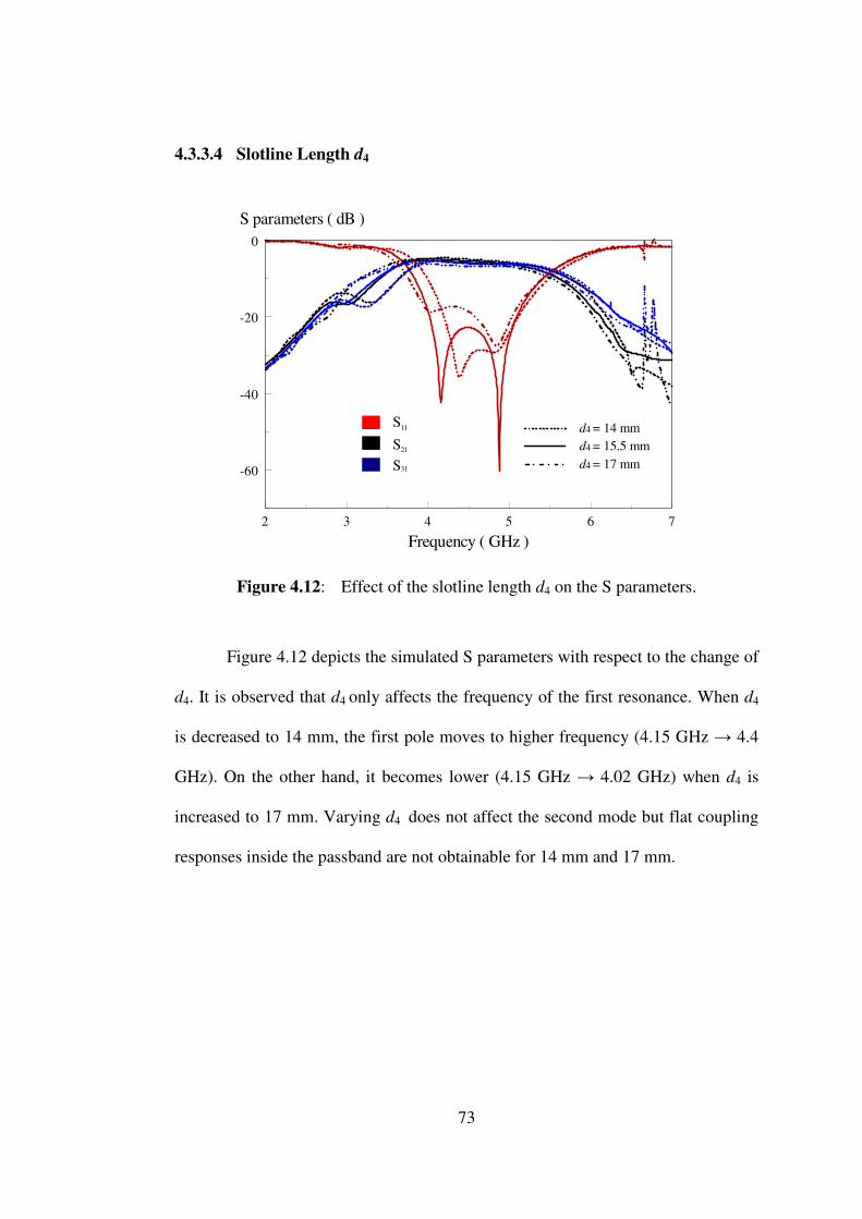
73
4.3.3.4 Slotline Length d4
Figure 4.12: Effect of the slotline length d4 on the S parameters.
Figure 4.12 depicts the simulated S parameters with respect to the change of
d4. It is observed that d4 only affects the frequency of the first resonance. When d4
is decreased to 14 mm, the first pole moves to higher frequency (4.15 GHz → 4.4
GHz). On the other hand, it becomes lower (4.15 GHz → 4.02 GHz) when d4 is
increased to 17 mm. Varying d4 does not affect the second mode but flat coupling
responses inside the passband are not obtainable for 14 mm and 17 mm.
2 3 4 5 6 7
-60
-40
-20
0
Frequency ( GHz )
S parameters ( dB )
S11
S21
S31
d4 = 15.5 mm
d4 = 14 mm
d4 = 17 mm

74
4.3.3.5 Slotline Widths b1 and b4
Figure 4.13 and 4.14 illustrate the simulated S parameters with changing
slotline width. With reference to both of the figures, it is observed that b1 affects
the second resonance while b4 affects the first one. From Figure 4.13, the first mode
shifts lower (4.88 GHz→4.75 GHz) when b1 is reduced to 0.4 mm. It moves higher
(4.88 GHz→5 GHz) when b1 is equal to 0.8 mm. The first resonance remains
unchanged (4.15 GHz) when b1 is altered. Referring to Figure 4.14, the first pole
shifts when b4 is varied while the second one remains (4.88 GHz). When b4 is
decreased to 0.5 mm, the first mode shifts lower (4.15 GHz→4.08 GHz). But it
goes higher (4.15 GHz→4.22 GHz) when b4 is made 1.5 mm.
Figure 4.13: Effect of the slotline width b1 on the S parameters.
2 3 4 5 6 7
-60
-40
-20
0
Frequency ( GHz )
S parameters ( dB )
S11
S21
S31
b1 = 0.6 mm
b1 = 0.4 mm
b1 = 0.8 mm

75
Figure 4.14: Effect of the slotline width b4 on the S parameters.
4.3.3.6 Stripline Lengths l2 and l3
Referring to Figure 4.15, the stripline length l2 does not affect the S
parameters much. This is because it is not in the direction of the standing waves.
Varying l2 slightly affects the operating frequency of the second pole. When l2 is
reduced to 5.5 mm, the second pole shifts higher (4.88 GHz → 5 GHz). It shifts to
4.82 GHz for a longer length of 7.5mm. Here, the optimum value for l2 is designed
to be 6.5mm, giving the best impedance matching. Similar trend has been observed
for the stripline l3 which is shown in Figure 4.16.
2 3 4 5 6 7
-60
-40
-20
0
Frequency ( GHz )
S parameters ( dB )
S11
S21
S31
b4 = 0.9 mm
b4 = 0.5 mm
b4 = 1.5 mm

76
Figure 4.15: Effect of the stripline length l2 on the S parameters.
Figure 4.16: Effect of the stripline length l3 on the S parameters.
2 3 4 5 6 7
-60
-40
-20
0
Frequency ( GHz )
S parameters ( dB )
S11
S21
S31
l2 = 6.5 mm
l2= 5.5 mm
l2 = 7.5 mm
2 3 4 5 6 7
-60
-40
-20
0
Frequency ( GHz )
S parameters ( dB )
S11
S21
S31
l3 = 7 mm
l3 = 6 mm
l3 = 8 mm
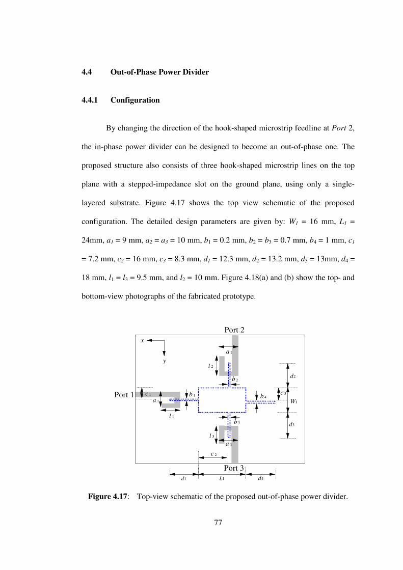
77
4.4 Out-of-Phase Power Divider
4.4.1 Configuration
By changing the direction of the hook-shaped microstrip feedline at Port 2,
the in-phase power divider can be designed to become an out-of-phase one. The
proposed structure also consists of three hook-shaped microstrip lines on the top
plane with a stepped-impedance slot on the ground plane, using only a single-
layered substrate. Figure 4.17 shows the top view schematic of the proposed
configuration. The detailed design parameters are given by: W1 = 16 mm, L1 =
24mm, a1 = 9 mm, a2 = a3 = 10 mm, b1 = 0.2 mm, b2 = b3 = 0.7 mm, b4 = 1 mm, c1
= 7.2 mm, c2 = 16 mm, c3 = 8.3 mm, d1 = 12.3 mm, d2 = 13.2 mm, d3 = 13mm, d4 =
18 mm, l1 = l3 = 9.5 mm, and l2 = 10 mm. Figure 4.18(a) and (b) show the top- and
bottom-view photographs of the fabricated prototype.
Figure 4.17: Top-view schematic of the proposed out-of-phase power divider.
y
x
d1 d4
d2
d3
L1
W1a 1
a 2
a 3
l 1
l 2
l 3
Port 1
Port 3
Port 2
b 1
b 2
b 3
b 4c 3
c 2
c 1

78
(a) (b) Figure 4.18: Prototype of the proposed out-of-phase power divider, (a) Top View,
(b) Bottom View.
4.4.2 Simulation and Experiment Results
In this section, the simulation and experiment results of the out-of-phase
power divider are illustrated and discussed. The simulated and measured S
parameters of the proposed configuration are shown in Figure 4.19(a). It has a
measured passband of 3.66 – 4.81 GHz (simulation: 3.84 – 5.0 GHz) with the
center frequency of 4.23 GHz (simulation: 4.41 GHz). The measured fractional
bandwidth (27.01%) is slightly larger than simulated one (26.21%), with output
coupling coefficient of less than 10 dB (in experiment)as illustrated in Figure
4.19(b). Figure 4.20 shows the calculated amplitude imbalance and phase
difference, which fall within ± 0.7 dB and180±3˚ in the passband, respectively.
Reasonable agreement is observed between the measurement and simulation
resultsfor the group delay in Figure 4.21. This is very positive as it shows that the
same piece of resonator can be made either as an in-phase or an out-of-phase power

79
divider. This interesting feature will be used to design the reconfigurable power
divider when incorporated with the RF pin diodes, which will be discussed in
Section 4.5.
(a)
(b)
Figure 4.19: Simulated and measured (a) reflection and transmission coefficients, and (b) isolation level between the output ports.
2 3 4 5 6 7-50
-40
-30
-20
-10
0
Frequency ( GHz )
S parameters ( dB )
Experiment
Simulation
S11
S21
S31
2 3 4 5 6 7
-50
-40
-30
-20
-10
0
Frequency ( GHz )
S parameters ( dB )
Experiment
SimulationS23
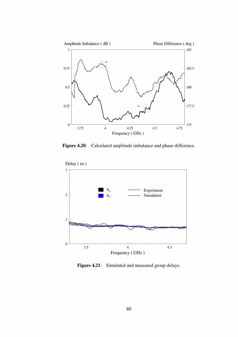
80
Figure 4.20: Calculated amplitude imbalance and phase difference.
Figure 4.21: Simulated and measured group delays.
3.75 4 4.25 4.5 4.750
0.25
0.5
0.75
1
175
177.5
180
182.5
185
Frequency ( GHz )
Amplitude Imbalance ( dB ) Phase Difference ( deg )
3.5 4 4.50
1
2
3
Frequency ( GHz )
Delay ( ns )
Experiment
Simulation
S21
S31

81
4.4.3 Theoretical and Parametric Studies
A theoretical study of the proposed out-of-phase power divider will be
made in this section. Figure 4.22 illustrates the simulated electric field distributions
of the stepped-impedance slot resonator at the two resonances (4.14 and 4.57 GHz).
It can be observed that the electric field patterns in Figure 4.22 are similar with
those in Figure 4.2(c) and 4.8 as an identical slot resonator has been used.With
respect to Figure 4.22(a), one field null is observed for the first resonance (4.14
GHz), but two for the second (4.57 GHz). Again, this slotline (Slotline4) is
positioned with a slight offset for a better impedance matching.
(a) (b)
Figure 4.22: The electric field distributions of the proposed out-of-phase power divider at the poles at (a) 4.14 GHz, and (b) 4.57 GHz.

82
4.4.3.1 Slot Length L1
Figure 4.23 illustrates the simulated S parameters with respect to the change
of the length of slotline L1. It is observed that the matching level and operating
bandwidth are greatly affected. When L1 is increased to 26 mm, the two poles are
moving closer to each other and, finally, combining at 4.32 GHz. The two
resonating modes move further apart (4.14 GHz → 4.11 GHz and 4.57 GHz →
4.83 GHz) when L1 is set to be 22 mm. Besides that, the amplitude imbalance
between the two output ports fluctuates for more than 1 dB across the passband
when L1 is varied.
Figure 4.23: Effect of the slot length L1 on the S parameters.
2 3 4 5 6 7-50
-40
-30
-20
-10
0
Frequency ( GHz )
S parameters ( dB )
S11
S21
S31
L1 = 24 mm
L1 = 22 mm
L1 = 26 mm

83
4.4.3.2 Slot Width W1
The optimum value for W1 is found to be 16mm. As can be seen from
Figure 4.24, when W1 is reduced to 14mm, the two poles combine into one at 4.41
GHz, narrowing the operating bandwidth. When increased to 18mm, the two poles
move further apart where the first mode is shifting to a lower frequency (4.14 GHz
→ 3.97 GHz) while the second is moving higher (4.57 GHz → 4.64 GHz). Flat
coupling response is not obtainable across the passband when W1 is altered.
Figure 4.24: Effect of the slot width W1 on the S parameters.
2 3 4 5 6 7-50
-40
-30
-20
-10
0
Frequency ( GHz )
S parameters ( dB )
S11
S21
S31
W1 = 16 mm
W1 = 14 mm
W1 = 18 mm
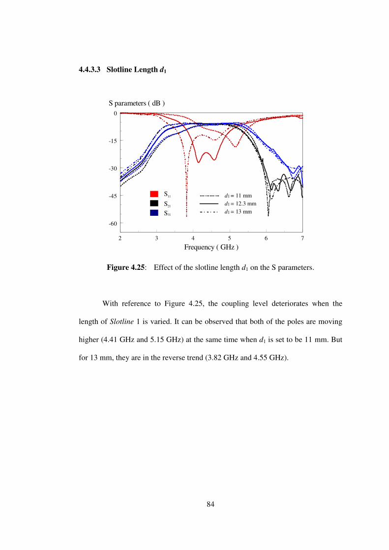
84
4.4.3.3 Slotline Length d1
Figure 4.25: Effect of the slotline length d1 on the S parameters.
With reference to Figure 4.25, the coupling level deteriorates when the
length of Slotline 1 is varied. It can be observed that both of the poles are moving
higher (4.41 GHz and 5.15 GHz) at the same time when d1 is set to be 11 mm. But
for 13 mm, they are in the reverse trend (3.82 GHz and 4.55 GHz).
2 3 4 5 6 7
-60
-45
-30
-15
0
Frequency ( GHz )
S parameters ( dB )
S11
S21
S31
d1 = 12.3 mm
d1 = 11 mm
d1 = 13 mm
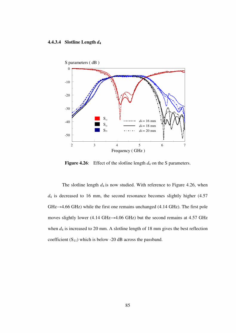
85
4.4.3.4 Slotline Length d4
Figure 4.26: Effect of the slotline length d4 on the S parameters.
The slotline length d4 is now studied. With reference to Figure 4.26, when
d4 is decreased to 16 mm, the second resonance becomes slightly higher (4.57
GHz→4.66 GHz) while the first one remains unchanged (4.14 GHz). The first pole
moves slightly lower (4.14 GHz→4.06 GHz) but the second remains at 4.57 GHz
when d4 is increased to 20 mm. A slotline length of 18 mm gives the best reflection
coefficient (S11) which is below -20 dB across the passband.
2 3 4 5 6 7
-50
-40
-30
-20
-10
0
Frequency ( GHz )
S parameters ( dB )
S11
S21
S31
d4 = 18 mm
d4 = 16 mm
d4 = 20 mm

86
4.4.3.5 Stripline Lengths l2 and l3
Figure 4.27: Effect of the stripline length l2 on the S parameters.
With reference to Figure 4.27, the S parameters are not affected much when
the stripline lengthl2is altered. When the l2value changes, the frequencies of the
poles are also varied. At l2 = 6.5 mm, the first pole shifts to a lower frequency (4.13
GHz→4.05 GHz) while the second one moves higher (4.57 GHz→4.67 GHz). It
does not affect the poles significantly when l2 is increased to 8.5mm. Similar trend
is also observed for the stripline l3, which is shown in Figure 4.28.
2 3 4 5 6 7-60
-50
-40
-30
-20
-10
0
Frequency ( GHz )
S parameters ( dB )
S11
S21
S31
l2 = 7.5 mm
l2 = 6.5 mm
l2 = 8.5 mm

87
Figure 4.28: Effect of the stripline length l3 on the S parameters.
2 3 4 5 6 7
-60
-40
-20
0
Frequency ( GHz )
S parameters ( dB )
S11
S21
S31
l3 = 7 mm
l3= 6 mm
l3 = 8 mm

88
4.5 Reconfigurable Power Divider
4.5.1 Configuration
In this section, the previously discussed in-phase and out-of-phase power
dividers are combined to form a new multifunctional device that can provide both
output phases in one, leading to cost saving. The schematic of the proposed
configuration is shown in Figure 4.29. In this new design, each output port is
incorporated with the BAR50-02V RF PIN diodes, manufactured by Infineon
Technologies. When the RF diode is reverse-biased, it can be used to block the RF
signal because of its low capacitance, for a better isolation. A RF diode is a good
conductor when it is forward-biased and let the RF signal to pass through. The
BAR50-02V RF PIN diode is chosen because of its good performance at high
frequency. In this project, two RF PIN diodes are used for each output port in order
to achieve isolation level of better than -20dB when it is in the OFF state (reverse-
biased).
The detailed design parameters are given by: W1 = 16 mm, L1 = 24 mm, a1
= 9 mm, a2 = a3 = 11.5mm, b1 = 0.2 mm, b2 = b3 = 0.7 mm, b4 = 1 mm, c1 = 7.9
mm, c2 = 16.5 mm, c3 = 9 mm, d1 = 12.3 mm, d2 = 12 mm, d3 = 12 mm, d4 = 16
mm, l1 = 9.5 mm, l2 = 10 mm, and l3 = 9 mm. The prototype of the proposed
structure is shown in Figure 4.30.

89
Figure 4.29: Schematic of the proposed reconfigurable power divider.
(a) (b) Figure 4.30: Prototype of the proposed reconfigurable power divider, (a) Top
View, (b) Bottom View.
Port 1
d1 d4
d2
d3
L1
W1a 1
a 2
a 3
l1
l3
DC block
RF PIN diode
y
x
Port 2Port 3
Port 4
l2
b 1b 4
b 2
b 2
c 3
c 2
c 1

90
4.5.2 Biasing Circuitry for RF PIN Diode
Figure 4.31 illustrates the biasing circuitry of the RF PIN diode. As can be
seen from the figure, the RF and DC signal paths are highlighted with red and blue
colors, respectively. In order to switch to ON state (forward-biased), the diodes are
biased with a voltage drop of 2 V. The RF choke (inductor) in the biasing circuitry
is used to avoid leakage of microwave signal to the DC path while the DC block
(capacitor) is used to prevent the DC signal from flowing into the proposed
configuration.
Figure 4.31: Biasing Circuitry for the RF PIN Diode.
RF choke
RF choke
DC block DC block
RF signal
DC signal
91
Referring to the datasheet, for each RF diode, the insertion loss is
approximately 0.3 dB, giving a 10mA forward current at 4 GHz. In OFF state
(reverse-biased), each diode is able to provide an isolation level of about -14 dB at
4 GHz. Placing the two diodes at each output port improves the isolation level to be
greater than -14 dB, avoiding microwave signals from reaching the unused ports
more effectively.
4.5.3 Simulation and Experimental Results
The proposed structure is first configured into the in-phase mode. By
reverse-biasing (OFF) the diodes, Port 2 can be easily disconnected. Port 3 and
Port 4 are set at ON state by forward-biasing the diodes. Figure 4.32 shows the
simulated and measured S parameters. The measured passband is 3.61 – 4.36 GHz
(simulation: 3.67 – 4.78 GHz) with a FBW of 19% (simulation:26%). It can be seen
from the figure that the measured and simulated center frequencies are 3.98 GHz
and 4.23 GHz, respectively, showing reasonable agreement with an error of 6.28%.
This result is acceptable for the active case. With the two diodes, the isolated level
(|S21|) is managed well below -25dB across the entire passband. This proves that the
BAR50-02V pin diode can give excellent isolation in the OFF state (reverse-
biased). With reference to Figure 4.33, it is observed that the amplitude imbalance
and phase difference between the two output ports (Port 3 and Port 4) fall within ≤
0.6 dB and ± 4.8˚, respectively, both of which are calculated from measurements.

92
Figure 4.32: Simulated and measured S parameters of the reconfigurable in-phase power divider (with Port 2 OFF but others ON).
Figure 4.33: Calculated amplitude imbalance and phase difference of the
reconfigurable in-phase power divider (with Port 2 OFF but others ON).
2 3 4 5 6 7
-50
-40
-30
-20
-10
0
Frequency ( GHz )
S parameters ( dB )
S11
S21
S31
S41
Experiment
Simulation
3.75 4 4.250
0.25
0.5
0.75
1
0
1
2
3
4
5
Frequency ( GHz )
Amplitude Imbalance ( dB ) Phase Difference ( deg )

93
Next, the configuration is made out-of-phase by turning the diodes into OFF
state at Port 3. Figure 4.34 shows the simulated and measured S parameters. The
measured and simulated center frequencies are 3.98 and 4.14 GHz, respectively,
with an error of 4.02%. The measured FBW (18.67%) is lower than the simulated
one (23.8%). The isolation level (|S31|) is measured ~ -20dB in the passband. The
amplitude imbalance and phase difference of the out-of-phase configuration are
shown in Figure 4.35, giving ≤0.54 dB and 180± 4.9˚ across the entire passband.
Figure 4.34: Simulated and measured S parameters of the reconfigurable out-of-phase power divider (with Port 3 OFF but others ON).
2 3 4 5 6 7-60
-50
-40
-30
-20
-10
0
Frequency ( GHz )
S parameters ( dB )
S11
S21
S31
S41
Experiment
Simulation

94
Figure 4.35: Calculated amplitude imbalance and phase difference of the reconfigurable out-of-phase power divider (with Port 3 OFF but others ON).
4.6 Conclusion
In this chapter, a passive in-phase, a passive out-of-phase, and a
reconfigurable power dividers have been proposed. In the first part, the passive
components are designed and optimized. It was found that the phase polarity of the
output signal is changeable by inverting the current direction of the hook-shaped
microstrip feedline. Next, the in-phase and out-of-phase power dividers are
combined to form a reconfigurable power divider. By incorporating several RF PIN
diodes into the output feedlines, the proposed active power divider is able to
3.75 4 4.250
0.25
0.5
0.75
1
175
177.5
180
182.5
185
Frequency ( GHz )
Amplitude Imbalance ( dB ) Phase Difference ( deg )

95
generate the in-phase or out-of-phase outputs. All the measured results show
reasonable agreement with the simulated ones.

96
CHAPTER 5
CONCLUSION
5.1 Conclusion
In this thesis, two different multifunctional couplers have been proposed. In
the first part, the multiport power-dividing directional coupler with multiple output
levels has been designed by using the microstrip rectangular patch resonator. This
multifunctional structure can produce half-powered division as well as coupled
signals (10 dB and 20 dB) at the same time. In the second, the stepped-impedance
slotline resonator has been explored for designing in-phase and out-of-phase
passive power dividers. By incorporating RF PIN diodes, the two passive
components can be combined, resulting in a reconfigurable component that can
provide either in-phase or out-of-phase operation at any one time. Experiments
have been conducted, showing reasonable agreement to simulations.
5.2 Future Work
The proposed structure in the first part of the project can be made even
more compact with the use of new technologies. Additional modes can also be
added to increase the fractional bandwidth. For the second part of the project, the

97
stepped-impedance slotline reconfigurable power divider may be made even more
versatile by including output ports to provide 45˚ and 90˚ phase differences.
Furthermore, the bandwidth of the proposed structure can be increased by adding
more resonances into the operating frequency passband.

98
Bibliography
1. S. L. Lim, E. H. Lim, and F. L. Lo, ‘Multifunctional Power-dividing
Directional Couplers with Multiple Output Levels’, IET Microwaves,
Antennas & Propagation. (Submitted)
2. S. L. Lim, E. H. Lim, and F. L. Lo, ‘Reconfigurable Stepped-impedance
Slotline Power Dividers’, IET Microwaves, Antennas & Propagation.
(Submitted)

99
References
A. A. Kishk and W. Huang, 2011 Size Reduction Method for Dielectric Resonator
Antenna, IEEE Antennas and Propag. Magazine, 53(2), pp. 26-38
A. A. Semenov, P. Yu. Beljavski, A. A. Nikitin, S. F. Karmanenko, B. A. Kalinikos
and G. Srinivasan, 2008 Dual Tunable Thin-film Ferrite-ferroelectric Slotline
Resonator, Electron. Lett., 44(24), pp. 1406-1407.
A. Bhardwaj and V. D. Kumar, 2012 Optical Dielectric Resonator Antenna,
International Conference Communications, pp. 159-162.
A. Dadgarpour, G. Dadashzadeh, M. Naser-Moghadasi, F. Jolani and B. S. Virdee,
2010 PSO/FDTD Optimization Technique for Designing UWB In-phase Power
Divider for Linear Array Antenna Application, IEEE Antennas and Wireless
Propag.Lett., 9, pp. 424-427.
A. S. S. Mohra, 2008 Compact Dual Band Wilkinson Power Divider, Radio
Science Conference, pp. 1-7.
Ansoft Corporation, High Frequency Structure Simulator (HFSS) v. 11 [Online].
Available: http://www.ansoft.com/products/hf/hfss/. [11 July 2010]
B. Li, X. Wu, Y. Li, J. Zhang and W. Wu, 2010 A Dual-Band Wilkinson Power
Divider with 6:1 Power Dividing Ratio Using Coupled Lines, IEEE Antennas and
Propag. Society International Symposium, pp. 1-4.
B. Li, X. Wu, C. Hua, N. Yang, D. Zhu and W. Wu, 2011 A Tri-band Wilkinson
Power Divider using Extended T-shaped Stubs, Microwave Conference
Proceedings, pp. 1-4.
100
C. H. Ho, L. Fan and K. Chang, 1993 Slot-Coupled Double-Sided Microstrip
Interconnects and Couplers, International Microw. Symp. Dig., 3, pp. 1321-1324.
C. H. Ng, E. H. Lim and K. W. Leung, 2011 Compact Microstrip Patch Balun
Filter, Cross Strait Quad-Regional Radiao Science and Wireless Tech. Conference,
1, pp. 1749-1751.
C. Lee, C. G. Hsu and C. Chen, 2012 Band-notched Balanced UWB BPF with
Stepped-Impedance Slotline Multi-mode Resonator, IEEE Microw. Wireless
Compon. Lett., 22(4), pp. 182-184.
C. Lin and S. Chung, 2011 A Compact Filtering 180o Hybrid, IEEE Trans. Microw.
Theory Tech., 59(12), pp. 3030-3036.
C. Wang and K. Chang, 2002 A 3-D Broadband Dual-layer
MultiapertureMicrostrip Directional Coupler, IEEE Microw. Wireless
Compon.Lett., 12(5), pp. 160-162.
D. Hawatmeh, N. Dib and K. A. Shamaileh, 2012 Design and Analysis of a 3-way
Unequal Split Ultra Wideband Wilkinson Power Divider, IEEE Antennas and
Propag. Society International Symp., pp. 1-2.
D. M. Pozar, 2011 Microwave Engineering, John Wiley & Sons, Inc., Fourth
Edition.
D. Woo and T. Lee, 2005 Suppression of Harmonics in Wilkinson Power Divider
using Dual-Band Rejection by Asymmetric DGS, IEEE Trans. Microw. Theory
Tech., 53(6), pp. 2139-2144.
E. A. Mariani, C. P. Heinzman, J. P. Agrios and S. B. Cohn, 1969 Slot Line
Characteristics, IEEE Trans. Microw. Theory Tech., 17(12), pp. 1091-1096.

101
E. H. Lim and K. W. Leung, 2012 Compact Multifunctional Antennas for Wireless
Systems, John Wiley & Sons, Inc.
E. J. Wilkinson, 1960 An N-way Hybrid Power Divider, IRE Trans. Microw.
Theory Tech., 8 (1), pp. 116-118.
F. Xu, G. Guo, E. Li and J. Wu, 2012 An Ultra-broadband 3-dB Power Divider,
Global Symp.on Millimeter Waves, pp. 347-350.
G. Elazar and M. Kisliuk, 1988 Microstrip Linear Slot Array Antenna for X-band,
IEEE Trans. Antennas Propag., 36(8), pp. 1144-1147.
H. Chen and Y. Pang, 2011 A Tri-band Wilkinson Power Divider utilizing Coupled
Lines, IEEE Antennas and Propag. Society International Symp., pp. 25-28.
H. Iwasaki, K. Kawabata and K. Yasukawa, 1990 A Circularly Polarized
Microstrip Antenna using a Crossed-Slot Feed, International Symp. Antennas
Propag. Society, 2, pp. 807-810.
H. Ma, Q. Chu and L. Ye, 2008 Wideband Uniplanar 180o Out-of-phase Power
Divider, Asia-Pacific Microw. Conference, pp. 1-4.
I. Wolff, 1972 MicrostripBandpass Filter using Degenerate Modes of a Microstrip
Ring Resonator, Electron. Lett., 8(12), pp. 302-303.
J. E. Ruyle and J. T. Bernhard, 2013 A Wideband Transmission Line Model for a
Slot Antenna, IEEE Trans. Antennas Propag., 61(3), pp. 1407-1410.
J. Kao, Z. Tsai, K. Lin and H. Wang, 2012 A Modified Wilkinson Power Divider
with Isolation Bandwidth Improvement, IEEE Trans. Microw. Theory Tech., 60(9),
pp. 2768-2780.

102
J. Lee, I. Jeon, Y. Cho, X. Wang and S. Yun, 2012 Design of Dual-band Power
Divider using Shunt Open-stubs with Enhanced Attenuation Characteristics, Asia-
Pacific Microw. Conference Proceedings, pp. 1199-1201.
J. Li and B. Wang, 2011 Novel Design of Wilkinson Power Dividers with Arbitary
Power Division Ratios, IEEE Trans. Industrial Electron., 58 (6), pp 2541-2546.
J. Li, J. Wang, X. Yang and B. Wang, 2010 A Study of Dual-mode Patch
Resonator-based Microwave Filter, International Conference on Microw. and
Millimeter Wave Tech., pp. 48-51.
J. Reed and G. J. Wheeler, 1956 A Method of Analysis of Symmetrical Four-Port
Networks, IRE Trans. Microw. Theory Tech., 4(4), pp. 246-252.
J. W. Burns, 1985 Planar, Quadrature Microwave Coupler, U. S. Patent, no.
4,492,939.
J. Wang, J. Ni, Y. Guo and D. Fang, 2009 Miniaturized Microstrip Wilkinson
Power Divider with Harmonic Suppression, IEEE Microw. Wireless Compon.Lett.,
19(7), pp. 440-442.
J. X. Chen, C. Y. Cheung and Q. Xue, 2007 Integrated Bandpass Filter Balun based
on Double-sided Parallel-strip Line with an Inserted Conductor Plane, Asia-Pacific
Microw. Conference, pp. 1-4.
J. Xiao, Q. Chu and Y. Wang, 2008 New Patch Resonator Bandpass Filter with
Wideband and Tunable Operation, Asia-Pacific Microw. Conference, pp. 1-3.
J. Yen, S. Hsu and T. Wu, 2011 A Novel Compact Backward-wave Directional
Coupler Design with Defected Ground Structure, Asia-Pacific Microw. Conference
Proceedings, pp. 1150-1153.

103
J. Yen, S. Hsu and T. Wu, 2011 A Novel Miniaturized Forward-wave Directional
Coupler Loaded with Periodic Shunt Inductors, European Microw. Conference, pp.
782-785.
K. A. O’Connor and R. D. Curry, 2012 A Dielectric Resonator Antenna based on
High Dielectric Constant Composites for High Power UHF Antenna Applications,
IEEE Power Modulator and High Voltage Conference, pp. 245-249.
K. C. Gupta and M. D. Abouzahra, 1985 Analysis and Design of Four-Port and
Five-Port Microstrip Disc Circuits, IEEE Trans. Microw. Theory Tech., 33(12), pp.
1422-1428.
K. Itoh and M. Yamamoto, 1997 A Slot-Coupled Microstrip Array Antenna with a
Triplate Line Feed where Parallel-Plate Mode is Suppressed Efficiently,
International Symp. Antennas Propag. Society, 4, pp. 2135-2138.
K. L. Chan, F. A. Alhargan and S. R. Judah, 1997 A Quadrature-hybrid Design
using a Four-port Elliptic Patch, IEEE Trans. Microw. Theory Tech., 45(2), pp.
307-310.
K.Song and Q. Xue, 2010 Novel Ultra-wideband (UWB) Multilayer Slotline Power
Divider with Bandpass Response, IEEE Microw. Wireless Compon.Lett., 20(1), pp.
13-15.
K. Song, Y. Fan and X. Zhou, 2008 Broadband Multilayer In-phase Power Divider,
Electron. Lett., 44(6), pp. 417-418.
K. Yi and B. Kang, 2003 Modified Wilkinson Power Divider for nth Harmonic
Suppression, IEEE Microw. Wireless Compon.Lett., 13(5), pp. 178-180.

104
L. Wu, B. Xia, W. Yin and J. Mao, 2013 Collaborative Design of a New Dual-
Bandpass 180 Hybrid Coupler, IEEE Trans. Microw. Theory Tech., 61(3), pp.
1053-1066.
M. A. Beldi, F. Boone and D. Deslandes, 2012 Design of Microstrip Power
Dividers with Filtering Functions, European Microw. Conference, pp. 384-387.
M. Aikawa and H. Ogawa, 1980 A New MIC Magic-T using Coupled Slotlines,
IEEE Trans. Microw. Theory Tech., 28(6), pp. 523-528.
M. D. Abouzahra and K. C. Gupta, 1988 Multiport Power Divider-Combiner
Circuits using Circular-Sector-Shaped Planar Components, IEEE Trans. Microw.
Theory Tech., 36(12), pp. 1747-1751.
M. Dydyk, 1999 Microstrip Directional Couplers with Ideal Performance via
Single-element Compensation, IEEE Trans. Microw. Theory Tech., 47(6), pp. 956-
964.
M. E. Bialkowski and A. M. Abbosh, 2007 Design of a Compact UWB Out-of-
phase Power Divider, IEEE Microw. Wireless Compon.Lett., 17(4), pp. 289-291.
M. E. Bialkowski and S. T. Jellett, 1994 A 3 dB Planar Coupler in the form of an
Elliptically Shaped Disc, IEEE Microw. Symp. Dig., 1, pp. 209-212.
M. E. Bialkowski and S. T. Jellett, 1994 Analysis and Design of a Circular Disc 3
dB Coupler, IEEE Trans. Microw. Theory Tech., 42(8), pp. 1437-1442.
M. E. Bialkowski, N. Seman and M. S. Leong, 2009 Design of a Compact Ultra
Wideband 3 dB Microstrip Slot Coupler with High Return Losses and Isolation,
Asia-Pacific Microw. Conference, pp. 1334-1337.

105
M. E. Bialkowski and Y. Wang, 2010 Wideband Microstrip 180o Hybrid utilizing
Ground Slots, IEEE Microw. Wireless Compon.Lett., 20(9), pp. 495-497.
M. E. Bialkowski and Y. Wang, 2011 UWB Planar Out-of-phase Wilkinson Power
Divider utilizing UWB ±90o Phase Shifters in Microstrip-slot Technology, Asia-
Pacific Microw. Conference Proceedings, pp. 1138-1141.
M. E. Goldfarb, 1991 A Recombinant, In-Phase Power Divider, IEEE Trans.
Microw. Theory Tech., 39 (8), pp 1438-1440.
M. Nakatsugawa and K. Nishikawa, 2001 A Novel Configuration for 1:N Multiport
Power Dividers using Series/Parallel Transmissin-line Division and a
Polyimide/Alumina-Ceramic Structure for HPA Module Implementation, IEEE
Trans. Microw. Theory Tech., 49(6), pp. 1187-1193.
M. Ohira, Z. Ma and M. Kato, 2011 Resonant-mode Behavior of a New Slotline
Embedded Three-mode Microstrip line Resonator and its Filter Application,
Microw. Conference Proceedings, pp. 1-4.
N. Behdad and K. Sarabandi, 2005 A Wide-band Slot Antenna Design Employing a
Fictitious Short Circuit Concept, IEEE Trans. Antennas Propag., 53(1), pp. 475-
482.
N. Yang, C. Caloz and K. Wu, 2010 Broadband Compact 180o Hybrid derived
from the Wilkinson Divider, IEEE Trans. Microw. Theory Tech., 58(4), pp. 1030-
1037.
P. Cheong, T. Lv, W. Choi and K. Tam, 2011 A Compact Microstrip Square-Loop
Dual-mode Balun-Bandpass Filter with Simultaneous Spurious Response
Suppression and Differential Performance Improvement, IEEE Microw. Wireless
Compon.Lett., 21(2), pp. 77-79.

106
P. Chi and T. Itoh, 2009 Miniaturized Dual-Band Directional Couplers Using
Composite Right/Left-Handed Transmission Structures and Their Applications in
Beam Pattern Diversity Systems, IEEE Trans. Microw. Theory Tech., 57(5), pp.
1207-1215.
P. K. Singh, S. Basu and Y. H. Wang, 2009 Coupled Line Power Divider with
Compact Size and Bandpass Response, Electron. Lett., 45(17), pp. 892-894.
Q. Li, J. Gong, X. Shi, X. Wang and F. Wei, 2010 A Compact Broadband
Multilayer In-phase Power Divider, International Conference on Microwav. And
Millimeter Wave Tech., pp. 756-758.
R. Zhang, L. Zhu and S. Luo, 2012 Dual-mode Dual-band Bandpass Filter using A
Single Slotted Circular Patch Resonator, IEEE Microw. Wireless Compon.Lett.,
22(5), pp. 233-235.
R. Zhang and R. R. Mansour, 2007 Low-cost Dielectric Resonator Filter with
Improved Spurious Performance, IEEE Trans. Microw. Theory Tech., 55(10), pp.
2168-2175.
S. B. Cohn, 1968 Slot Line - An Alternative Transmission Medium for Integrated
Circuits, International Microw. Symp., pp. 104-109.
S. B. Cohn, 1969 Slot Line on a Dielectric Substrate, IEEE Trans. Microw. Theory
Tech., 17(10), pp. 768-778.
S. Gruszcynski and K. Wincza, 2007 Broadband Multisection Asymmetric 8.34-dB
Directional Coupler with Improved Directivity, Asia-Pacific Microw. Conference,
pp. 1-4.

107
S. Hsu, C. Tsai and T. Wu, 2010 A Novel Miniaturized Forward-wave Directional
Coupler with Periodical Mushroom-shaped Ground Plane, IEEE Trans. Microw.
Theory Tech., 58(8), pp. 2277-2283.
S. Lin, M. Eron, S. Turner and J. Sepúlveda, 2011 Development of Wideband Low-
loss Directional Coupler with Suspended Stripline and Microstrip Line, Electron.
Lett., 47 (25), pp. 1377-1379.
S. Mao and M. Wu, 2007 A Novel 3-dB Directional Coupler with Broad
Bandwidth and Compact Size using Composite Right/Left-handed Coplanar
Waveguides, IEEE Microw. Wireless Compon.Lett., 17(5), pp. 331-333.
S. R. Zinka, A. Mohan and A. Biswas, 2007 Bandpass Filter Realization using
Degenerate Dual-modes of a New Type of Patch Resonator for Significant Size
Reduction, Asia-Pacific Microw. Conference, pp. 1-4.
S. Sun and L. Zhu, 2010 Miniaturized Patch Hybrid Couplers using
Asymmetrically Loaded Cross Slots, IET Microw. Antennas and Propag., 4(9), pp.
1427-1433.
S. Sun and W. Menzel, 2011 Novel Dual-mode BalunBandpass Filters using Single
Cross-Slotted Patch Resonator, IEEE Microw. Wireless Compon.Lett., 21(8), pp.
415-417.
S. W. Wong and L. Zhu, 2008 Ultra-wideband Power Divider with Good In-band
Splitting and Isolation Performance, IEEE Microw. Wireless Compon.Lett., 18(8),
pp. 518-520.
S. Y. Zheng, S. H. Yeung, W. S. Chan, K. F. Man and S. H. Leung, 2009 Size-
Reduced Rectangular Patch Hybrid Coupler using Patterned Ground Plane, IEEE
Trans. Microw. Theory Tech., 57(1), pp. 180-188.

108
T. Kawai, I. Ohta, M. Nishimura and T. Kaneko, 1992 A Rectangular Disk 3 dB
Quadrature Hybrid with Flat Coupling, Asia-Pacific Microw. Conference, 2, pp.
673-676.
T. Tanaka, K. Tsunoda and M. Aikawa, 1988 New Slot-Coupled Directional
Couplers between Double-Sided Substrate Microstrip Lines, and Their
Applications, International Microw. Symp. Dig., 2, pp. 579-582.
V. F. Fusco and J. A. C. Stewart, 1986 Design and Synthesis of Patch Microwave
Couplers, European Microw. Conference, pp. 401-406.
V. F. Fusco and L. N. Merugu, 1990 Full Wave Analysis of 94 GHz Patch Coupler,
International Microw. Symp. Dig., 2, pp. 649-652.
W. Liu, F. Wei, C. Pang and X. Shi, 2012 Design of A Compact Ultra-wideband
Power Divider, International Conference on Microw. and Millimeter Wave Tech., 2,
pp. 1-3.
X. D. Huang, C. H. Cheng and L. Zhu, 2012 An Ultrawideband (UWB) Slotline
Antenna under Multiple-Mode Resonance, IEEE Trans. Antennas Propag., 60(1),
pp. 385-389.
X. Li, Y. Yang, L. Yang, S. Gong, T. Hong, X. Chen and Y. Zhang, 2009 Design
of Unequal Wilkinson Power Divider for Dual-band Operation with Isolation Stubs,
Electron. Lett., 45(24), pp. 1245-1247.
X. Ou and Q. Chu, 2008 A Modified Two-section UWB Wilkinson Power Divider,
International Conference Microw, and Millimeter Wave Tech., 3, pp. 1258-1260.
X. Wang, Y. Bai, H. Xu, W. Cheng and X. Shi, 2011 A Tri-band Wilkinson Power
Divider using Step-impedance Resonator, IEEE Electrical Design of Advanced
Packaging and Systems Symp., pp. 1-4.

109
Y. J. Cheng, W. Hong, K. Wu and Y. Fan, 2011 A Hybrid Guided-Wave Structure
of Half Mode Substrate Integrated Waveguide and Conductor-Backed Slotline and
its Application in Directional Couplers, IEEE Microw. Wireless Compon.Lett.,
21(2), pp. 65-67.
Y. Lu, S. Chen and P. Hsu, 2012 A Differential-mode Wideband Bandpass Filter
with Enhanced Common-mode Suppression using Slotline Resonator, IEEE
Microw. Wireless Compon.Lett., 22(10), pp. 503-505.
Y. Wu, X. Xie, R. Xu, X. Zhao and S. Xie, 2012 Analysis and Design of A Novel
Coupled-line Wideband Wilkinson Power Divider, International Conference
Microw, and Millimeter Wave Tech., 3, pp. 1-4.
Y. Wu, Y. Liu and Q. Xue, 2011 An Analytical Approach for a Novel Coupled-line
Dual-band Wilkinson Power Divider, IEEE Trans. Microw. Theory Tech., 59(2), pp.
286-294.