DESIGN OF HIGH-SPEED OPTICAL …spalermo/docs/thesis_sam_palermo.pdfdesign of high-speed optical...
174
DESIGN OF HIGH-SPEED OPTICAL INTERCONNECT TRANSCEIVERS A DISSERTATION SUBMITTED TO THE DEPARTMENT OF ELECTRICAL ENGINEERING AND THE COMMITTEE ON GRADUATE STUDIES OF STANFORD UNIVERSITY IN PARTIAL FULFILLMENT OF THE REQUIREMENTS FOR THE DEGREE OF DOCTOR OF PHILOSOPHY Samuel Palermo September 2007
Transcript of DESIGN OF HIGH-SPEED OPTICAL …spalermo/docs/thesis_sam_palermo.pdfdesign of high-speed optical...

DESIGN OF HIGH-SPEED OPTICAL INTERCONNECT TRANSCEIVERS
A DISSERTATION
SUBMITTED TO THE DEPARTMENT OF ELECTRICAL ENGINEERING
AND THE COMMITTEE ON GRADUATE STUDIES
OF STANFORD UNIVERSITY
IN PARTIAL FULFILLMENT OF THE REQUIREMENTS
FOR THE DEGREE OF
DOCTOR OF PHILOSOPHY
Samuel Palermo
September 2007

ii
© Copyright by Samuel Palermo 2007
All Rights Reserved

iii
I certify that I have read this dissertation and that, in my opinion, it is fully adequate in scope and quality as a dissertation for the degree of Doctor of Philosophy.
__________________________________ (Mark A. Horowitz) Principal Adviser
I certify that I have read this dissertation and that, in my opinion, it is fully adequate in scope and quality as a dissertation for the degree of Doctor of Philosophy.
__________________________________ (David A. B. Miller)
I certify that I have read this dissertation and that, in my opinion, it is fully adequate in scope and quality as a dissertation for the degree of Doctor of Philosophy.
__________________________________ (Bruce A. Wooley)
Approved for the University Committee on Graduate Studies

iv

v
Abstract
The increase in computing power enabled by CMOS scaling has created increased
demand for chip-to-chip I/O bandwidth. Unfortunately, inter-chip electrical channel
bandwidth has not scaled similarly to on-chip performance, causing current high-speed
I/O link designs to be channel limited and require sophisticated equalization circuitry
which increases power consumption. Interconnect architectures which employ optical
channels have negligible frequency dependent loss and provide a potential path to
increased I/O bandwidth without excessive circuit complexity or power consumption.
This dissertation focuses on a dense low-power CMOS optical link architecture
which employs novel optical transmitter and receiver circuits and leverages an
electrical link technique of time-division multiplexing in order to achieve high-speed
operation. Transmitter designs are demonstrated for the two primary high-density
optical sources, vertical-cavity surface-emitting lasers (VCSEL) and multiple-
quantum-well modulators (MQWM). The implemented VCSEL driver employs
simple transmitter equalization techniques in order to extend the effective device
bandwidth for a given reliability level. For the MQWM devices, a pulsed-cascode
driver supplies an output voltage swing of twice the nominal CMOS power supply
without overstressing thin oxide core devices. A low-voltage integrating and double-
sampling optical receiver provides adequate sensitivity in a power-efficient manner by
avoiding linear high-gain elements. In order to address this receiver’s inability to

vi
handle uncoded data, a swing control filter which actively clamps the input signal
within the receiver input range is investigated.
Transmitter clock generation uses an adaptive bandwidth phase-locked loop
(PLL) for a wide frequency range, while receiver timing recovery is implemented with
a dual-loop architecture which employs baud-rate phase detection and feedback
interpolation to achieve reduced power consumption. High-precision phase spacing is
ensured at both the transmitter and receiver through adjustable delay clock buffers
applied independently on a per-phase basis.
Implemented in a standard 1V 90nm CMOS process, the transceiver operates at
data rates between 5 to 16Gb/s. At 16Gb/s, the measure power consumption is
129mW for the VCSEL-based link and projected at 103mW for the modulator-based
link, with both links occupying an area close to 0.1mm2.

vii
Acknowledgments
In the time I spent at Stanford, I was able to experience an enormous amount of
educational, professional, and personal growth due to the guidance and support of
many people.
I am very lucky to have had the opportunity to work with an excellent research
advisor, Prof. Mark Horowitz. His unequivocal technical expertise, teaching skills,
and the unique ability to motivate through simultaneously challenging and
encouraging ideas place him at the apex of the scientific research community. Mark’s
mentoring served as a key stabilizing force as I experienced the ebb and flow of
doctoral research.
I would also like to especially thank some of the key faculty and researchers that I
had the pleasure of working with at Stanford. I am grateful to my associate advisor,
Prof. Miller, for introducing me to the exciting field of photonics and showing me
many amazing technological applications. I would like to thank him for providing me
the opportunity to collaborate with his students on several projects and for being a
member of my oral defense and reading committees. I gratefully acknowledge Prof.
Bruce Wooley for his teaching, support, and for taking the time to read this thesis. I
also thank Dr. Tim Drabik for expanding my knowledge of VCSELs.
I have truly enjoyed and greatly benefited from the interaction with an amazing
group of research colleagues at Stanford. I am extremely indebted to Azita Emami-

viii
Neyestanak, with whom I collaborated on much of the optical high-speed link work.
Special thanks are also in order for Bita Nezamfar, Dinesh Patil, and Patrick Chang for
their assistance at various stages in the design of my final optical interconnect test-
chip. I am grateful for the opportunity to collaborate on research projects with Aparna
Bhatnagar and Jon Roth from Prof. Miller’s group. For their technical interaction and
friendship, I would like to thank the following members of the Horowitz Group: Hae-
Chang Lee, Vladimir Stojanović, Elad Alon, Dean Liu, Valentin Abramazon, Ken
Mai, Jaeha Kim, Amir Amirkhany, Xiling Shen, Ron Ho, Jim Weaver, Bennett
Wilburn, Francois Labonte, and Alex Solomatnikov. Also, from Prof. Miller’s Group,
Salman Latif, Noah Helman, and Henry Chin deserve special recognition.
I wish to thank the National Science Foundation, MARCO IFC, and Texas
Instruments for their financial support. Also, donated resources from ST
Microsystems, National Semiconductor, CMP, Emcore, Ulm Photonics, and Albis
Optoelectronics enabled this research. Special thanks are in order for Bhusan Gupta
and Greg Watson for assisting in establishing CAD infrastructure. I also sincerely
thank Teresa Lynn, Penny Chumley, and Ann Guerra for their administrative support
The circuit design knowledge and experience I gained from my studies at Texas
A&M University allowed me to hit the ground running at Stanford. For this, I thank
Dr. José Pineda de Gyvez, Prof. Edgar Sánchez-Sinencio, and Dr. Sherif H. K.
Embabi.
My parents have been a source of encouragement and support throughout my life.
I especially thank my mother Georgia for her unconditional love and strength, which
continued even after I moved her grandson halfway across the country. I also thank
my other parents (in-laws), Tom Ed and Michelle, for their unwavering love and
support. Finally, I am forever indebted to my wife Shawn and two sons, Nicholas and
Kyle, whose immeasurable love has supported me throughout this journey. For that, I
dedicate this thesis to them.

ix
Table of Contents
Abstract .........................................................................................................................v
Acknowledgments.......................................................................................................vii
Table of Contents......................................................................................................... ix
List of Tables................................................................................................................xi
List of Figures .............................................................................................................xii
Chapter 1 Introduction ................................................................................................1 1.1 Organization ......................................................................................................... 3
Chapter 2 Background.................................................................................................5 2.1 High-Speed Electrical Links.................................................................................5
2.1.1 Electrical Link Circuits..................................................................................6 2.1.2 Electrical Channels ......................................................................................12 2.1.3 Channel Equalization and Advanced Modulation Techniques ...................15
2.2 High-Speed Optical Links .................................................................................. 21 2.2.1 Optical Channels .........................................................................................22 2.2.2 Optical Transmitters ....................................................................................24 2.2.3 Optical Receivers.........................................................................................33
2.3 Summary.............................................................................................................36
Chapter 3 Optical Transmitter Design.....................................................................38 3.1 Multiplexing Transmitter....................................................................................39
3.2 VCSEL Driver Output Stage ..............................................................................41 3.2.1 Equalization.................................................................................................41 3.2.2 VCSEL Driver Output Stage Implementation.............................................46 3.2.3 Power and Area Overheads of the Equalizing Transmitter .........................49

x
3.2.4 Experimental Results...................................................................................52
3.3 Modulator Driver Output Stage..........................................................................55 3.3.1 Previous High-Voltage Output Stage Implementations ..............................56 3.3.2 Modulator Driver Output Stage Implementation ........................................58 3.3.3 Experimental Results...................................................................................66
3.4 Summary.............................................................................................................70
Chapter 4 Optical Receiver Design...........................................................................71
4.1 Low-Voltage Integrating and Double-Sampling Front-End............................... 72 4.1.1 Receiver Operation......................................................................................72 4.1.2 Receiver Segments ......................................................................................75 4.1.3 Average Current Generation........................................................................88 4.1.4 Receiver Performance Analysis ..................................................................91
4.2 Input Swing Control Filter..................................................................................96 4.2.1 Swing Control Filter Overview ...................................................................97 4.2.2 Swing Control Filter Circuits ....................................................................101 4.2.3 Swing Control Filter Performance Issues.................................................. 105
4.3 Experimental Results........................................................................................108
4.4 Summary...........................................................................................................114
Chapter 5 Clock Generation and Recovery ...........................................................115 5.1 Clock Generation.............................................................................................. 116
5.1.1 PLL Circuits ..............................................................................................117
5.2 Clock Recovery ................................................................................................122 5.2.1 Phase Detection .........................................................................................123 5.2.2 Dual-Loop CDR ........................................................................................ 126
5.3 Per-Phase Clock Adjustment ............................................................................129
5.4 Experimental Results........................................................................................131
5.5 Summary...........................................................................................................135
Chapter 6 Conclusions .............................................................................................137
6.1 Optical Link Performance Summary................................................................139
6.2 Electrical I/O Comparison and Projections ......................................................141
Bibliography..............................................................................................................144

xi
List of Tables
Table 3.1: Interconnect and VCSEL simulation parameters .......................................42
Table 3.2: VCSEL transmitter performance summary................................................55
Table 3.3: MQW modulator transmitter performance summary.................................69
Table 4.1: Integrating receiver sensitivity parameters ................................................95
Table 4.2: Optical receiver performance summary ...................................................113
Table 5.1: Data patterns with phase information for baud-rate phase detection .......126
Table 5.2: Clocking circuitry performance summary................................................135

xii
List of Figures
Figure 1.1: I/O scaling necessity: (a) performance disparity between networking/on-
chip processing and off-chip bandwidth [2-4], (b) I/O scaling projections [5] ...... 2
Figure 1.2: Wavelength division multiplexing chip-to-chip optical interconnect [12] .2
Figure 2.1: High-speed electrical link system ............................................................... 6
Figure 2.2: Transmitter output stages: (a) current-mode driver, (b) voltage-mode
driver.......................................................................................................................7
Figure 2.3: Receiver input stage with regenerative latch [26].......................................8
Figure 2.4: Time-division multiplexing link .................................................................9
Figure 2.5: PLL frequency synthesizer .........................................................................9
Figure 2.6: PLL-based CDR system............................................................................ 11
Figure 2.7: CDR phase detectors: (a) linear [35], (b) binary [36] ..............................11
Figure 2.8: Backplane system cross-section................................................................ 13
Figure 2.9: Frequency response of several backplane channels [41] ..........................14
Figure 2.10: Backplane channel performance at 5Gb/s: (a) pulse response, (b) eye
diagram .................................................................................................................14
Figure 2.11: TX equalization with an FIR filter..........................................................16
Figure 2.12: RX equalization with an FIR filter..........................................................17
Figure 2.13: Continuous-time equalizing amplifier ....................................................18
Figure 2.14: RX equalization with a DFE ...................................................................19

xiii
Figure 2.15: Pulse amplitude modulation – simple binary PAM-2 (1bit/symbol) and
PAM-4 (2bits/symbol)..........................................................................................20
Figure 2.16: Optical fiber cross-section ......................................................................23
Figure 2.17: VCSEL: (a) device cross-section, (b) electrical model..........................25
Figure 2.18: VCSEL optical power versus current (L-I) curve...................................26
Figure 2.19: Modeled VCSEL frequency response: (a) electrical model junction
resistance current, (b) rate-equation model optical power, (c) cumulative optical
power ....................................................................................................................27
Figure 2.20: VCSEL MTTF versus average current [75,76].......................................30
Figure 2.21: VCSEL current-mode driver...................................................................31
Figure 2.22: MQWM: (a) device cross-section [84], (b) quantum-confined Stark
effect of AlGaAs/GaAs quantum wells [86] ........................................................ 32
Figure 2.23: MQWM electrical model ........................................................................32
Figure 2.24: MQWM voltage-mode driver .................................................................33
Figure 2.25: Optical receiver with transimpedance amplifier (TIA) input stage and
following limiting amplifier (LA) stages..............................................................35
Figure 3.1: Time-division multiplexing transmitter: (a) block digram, (b) circuit
implementation [18] .............................................................................................40
Figure 3.2: Equalizing VCSEL transmitter simulation model ....................................42
Figure 3.3: Simulated VCSEL frequency response: (a) flip-chip bond case, (b) wire
bond case .............................................................................................................. 43
Figure 3.4: Simulated 16Gbps pulse response of VCSEL with Iavg=5mA: (a) flip-
chip bond case, (b) wire bond case......................................................................44
Figure 3.5: Simulated maximum data rate versus Iavg: (a) flip-chip bond case, (b) wire
bond case .............................................................................................................. 44
Figure 3.6: VCSEL transmitter....................................................................................47
Figure 3.7: VCSEL transmitter synchronization circuitry ..........................................48
Figure 3.8: Simulated transmitter power dissipation at 13Gbps with various equalizer
filter lengths – wire bond case..............................................................................50

xiv
Figure 3.9: Simulated power dissipation versus data rate for various equalizer lengths:
(a) flip-chip bond case, (b) wire bond case ..........................................................51
Figure 3.10: Simulated power dissipation normalized by data rate for various
equalizer lengths: (a) flip-chip bond case, (b) wire bond case ..........................52
Figure 3.11: Commercial 10Gbps VCSEL wirebonded to VCSEL transmitter..........53
Figure 3.12: VCSEL transmitter optical test setup......................................................53
Figure 3.13: VCSEL optical power and voltage versus DC current ........................... 54
Figure 3.14: 18Gbps VCSEL optical eye diagrams (ER=3dB): (a) without
equalization, (b) with equalization .......................................................................54
Figure 3.15: VCSEL maximum data rate versus average current: (a) ER=3dB, (b)
ER=6dB ................................................................................................................55
Figure 3.16: High-voltage output stages: (a) static-biased cascode [100], (b) double-
cascode [102]........................................................................................................57
Figure 3.17: Transient simulation of a falling transition: static-cascode output stage
(a) nMOS drain voltages (b) nMOS drain-source voltages; double-cascode
output stage (c) nMOS drain voltages (d) nMOS drain-source voltages ............ 58
Figure 3.18: Pulsed-cascode output stage ...................................................................59
Figure 3.19: Transient simulation of pulsed-cascode output stage: falling transition
(a) nMOS gate voltages (b) nMOS drain voltages (c) nMOS Vgs and Vds, rising
transition (d) pMOS gate voltages (e) pMOS drain voltages (f) pMOS |Vgs| and
|Vds| .......................................................................................................................60
Figure 3.20: Simulated average output 10-90% transition time versus load-to-input
capacitance ratio for static-cascode, double-cascode, pulsed-cascode, and I/O
inverter based drivers............................................................................................61
Figure 3.21: Simulated power consumption versus bit rate for static-cascode, double-
cascode, pulsed-cascode, and I/O inverter based drivers. ....................................63
Figure 3.22: Modulator transmitter with level shifting multiplexer............................64
Figure 3.23: Simulated coupling capacitor skew attenuation between “high” and
“low” signal paths.................................................................................................65

xv
Figure 3.24: Simulated output stage absolute maximum voltages for random data
inputs: (a) nMOS transistors, (b) pMOS transistors ............................................66
Figure 3.25: Simulated distribution of MN1 maximum Vds – 200 Monte Carlo runs 66
Figure 3.26: Modulator transmitter on optical transceiver test chip. Modulators
pictured here are similar to the 850nm AlGaAs devices in [84]. ......................... 67
Figure 3.27: Analog sampler for monitoring modulator transmitter output................68
Figure 3.28: Subsampled 16Gb/s MQWM transmitter electrical eye diagram...........68
Figure 3.29: Optical 1Gb/s pseudo-eye diagram. ........................................................69
Figure 4.1: Emami’s integrating and double-sampling receiver [13]..........................73
Figure 4.2: Input voltage waveform and sampling clocks used to generate differential
voltage .................................................................................................................. 74
Figure 4.3: Input demultiplexing receiver using multiple sampler clock phases ........75
Figure 4.4: Sense-amplifier with capacitive offset correction.....................................76
Figure 4.5: Unit trim capacitance versus gate voltage for Offset=Vdd and Gnd ........78
Figure 4.6: Sense-amplifier input-referred offset correction and 3-sigma offset
magnitude versus input common-mode voltage level ..........................................79
Figure 4.7: Sense-amplifier delay versus input common-mode voltage level with the
maximum offset correction capacitance value .....................................................80
Figure 4.8: Modified SR-latch [108] ........................................................................... 82
Figure 4.9: Sense-amplifier kickback charge ..............................................................82
Figure 4.10: Receiver bit segment sense-amplifier waveforms at 2FO4 bit period
operation showing the negative effects of kickback charge .................................83
Figure 4.11: Modified receiver bit segment with differential buffer...........................84
Figure 4.12: Buffered sense-amplifier delay versus buffer input common-mode
voltage level with the maximum offset correction capacitance value.................. 84
Figure 4.13: Buffered sense-amplifier input-referred offset correction and 3-sigma
offset magnitude versus input common-mode voltage level ................................85
Figure 4.14: Receiver bit segment with buffered sense-amplifier waveforms at 2FO4
bit period operation showing improved transient performance............................86
Figure 4.15: Sampler rise-time versus common-mode voltage level ..........................88

xvi
Figure 4.16: Average current generation feedback loop .............................................89
Figure 4.17: Average current variation versus received data DC balance length .......90
Figure 4.18: Average current generation feedback amplifier and segmented output
current source .......................................................................................................91
Figure 4.19: Theoretical integrating receiver performance: (a) sensitivity versus data
rate, (b) dynamic range versus DSV.....................................................................95
Figure 4.20: Integrate and dump receiver....................................................................97
Figure 4.21: Input node of modified integrating receiver with added switched current
sources that form the swing control filter: (a) original proposition [110], (b)
transformed for practical implementation ............................................................99
Figure 4.22: Input voltage, net current, and dynamic offset values for the integrating
receiver with swing control filter (LD=6bits)..................................................... 100
Figure 4.23: Theoretical integrating receiver dynamic range versus DSV with and
without swing control filter ................................................................................101
Figure 4.24: Integrating receiver with swing control filter .......................................102
Figure 4.25: Switched IΔ current source....................................................................103
Figure 4.26: I0 and IΔ control loop locking behavior; I0=30μA, I1=140μA, IΔ=110μA
............................................................................................................................104
Figure 4.27: Sense-amplifier dynamic offset generation ..........................................105
Figure 4.28: Swing control filter critical path ...........................................................106
Figure 4.29: I0 and IΔ control loop locking behavior with 20% ΔVb offset and σn=13%
ΔVb; I0=30μA, I1=140μA, IΔ=110μA.................................................................107
Figure 4.30: IΔ phase error effect on input voltage waveform ..................................108
Figure 4.31: 850nm photodiodes wirebonded to optical receivers............................109
Figure 4.32: Optical link test setup............................................................................109
Figure 4.33: Integrating receiver input node response to a 10Gb/s 20bit repeating
pattern. Note from the on-die measurement, bits 3 and 13 are somewhat distorted
due to periodic noise on the subsamplers supply that is believed to not be present
on the input waveform........................................................................................110
Figure 4.34: Measured integrating receiver sensitivity versus data rate ...................111

xvii
Figure 4.35: Simulated impact of photodiode wirebond connection on the receiver’s
sampled differential input voltage at 16Gb/s: (a) no bondwire, (b) 0.3nH
bondwire .............................................................................................................111
Figure 4.36: Integrating receiver with swing control filter input node response to a
10Gb/s 20bit repeating pattern. Note the voltage ripples in the ideally flat part of
the input waveform due to a phase error in the IΔ current source, similar to the
simulation results of Figure 4.30. .......................................................................113
Figure 5.1: Clock generation PLL.............................................................................117
Figure 5.2: Coupled ring oscillator [29] ....................................................................118
Figure 5.3: Linear regulator for VCO supply filtering ..............................................119
Figure 5.4: Clock generation PLL phase-frequency detector....................................120
Figure 5.5: Charge-pump and loop filter ................................................................... 121
Figure 5.6: CDR bangbang phase detector................................................................123
Figure 5.7: Input voltage waveform with 2x-oversampling phase detection [98] ....124
Figure 5.8: Phase update probability for 2x-oversampling and baud-rate phase
detection.............................................................................................................. 124
Figure 5.9: Input voltage waveform with baud-rate phase detection [98] ................125
Figure 5.10: Dual-loop CDR for a 5:1 input demultiplexing receiver ......................127
Figure 5.11: Digital phase interpolator......................................................................128
Figure 5.12: Dual-loop CDR with feedback interpolation [95] ................................129
Figure 5.13: Adjustable delay clock buffer ............................................................... 130
Figure 5.14: Adjustable delay buffer tuning range versus normalized tuning
capacitance, 2FO4 UI .........................................................................................131
Figure 5.15: Clock phase muxes for off-chip measurements ....................................132
Figure 5.16: VCO frequency versus control voltage.................................................132
Figure 5.17: Clock jitter performance: (a) frequency synthesis PLL, (b) CDR
recovered clock...................................................................................................133
Figure 5.18: Interpolator performance: (a) phase positions, (b) DNL and INL .......134
Figure 5.19: Receiver clock phase tuning performance ............................................135

xviii
Figure 6.1: Optical link power consumption versus data rate. VCSEL link power is
experimentally measured, while MQWM power is projected assuming 100fF
modulators and a source laser with 6dB wall-plug efficiency............................140
Figure 6.2: Optical link power breakdown at 16Gb/s: (a) VCSEL link, (b) MQWM
link (projected) ...................................................................................................140
Figure 6.3: Optical versus electrical transceiver performance comparisons: (a) energy
efficiency, (b) circuit area...................................................................................141

1
Chapter 1 Introduction
Integrated circuit scaling has enabled a huge growth in processing power which
necessitates a corresponding increase in inter-chip communication bandwidth [1].
However, as shown in Figure 1.1(a), I/O bandwidth scaling has lagged behind the
processor performance gains [2- 34].
The two conventional methods for closing this performance gap include increasing
both the per-pin data rate and the I/O number, as projected in [4F5] ( 351HFigure 1.1(b)). While
high-performance I/O circuitry can leverage the technology improvements that enable
increased core performance, unfortunately the bandwidth of the electrical channels used
for inter-chip communication has not scaled in the same manner. Thus, rather than being
technology limited, current high-speed I/O link designs are becoming channel limited. In
order to continue scaling data rates, link designers implement sophisticated equalization
circuitry to compensate for the frequency dependent loss of the bandlimited channels [5F6-
6F7F8]. With this additional complexity comes both power and area costs, which will
ultimately limit the I/O number.

CHAPTER 1. INTRODUCTION
2
(a) (b)
Figure 1.1: I/O scaling necessity: (a) performance disparity between networking/on-chip processing and off-chip bandwidth [352H2- 353H354H4], (b) I/O scaling projections [355H5]
A promising solution to this I/O bandwidth problem is the use of optical inter-chip
communication links. The negligible frequency dependent loss of optical channels
provides the potential for optical link designs to fully leverage increased data rates
provided through CMOS technology scaling without the necessity of additional
equalization complexity. Optics also allows very high information density in both free-
space systems [8F9- 9F10F11], with the ability to focus short wavelength optical beams into small
areas without the crosstalk issues of electrical links, and in fiber-based systems, with the
added dimension of wavelength division multiplexing (WDM) ( 356HFigure 1.2) [11F12] where
multiple parallel links are multiplexed on one fiber by using different wavelength (color)
light for each link.
Figure 1.2: Wavelength division multiplexing chip-to-chip optical interconnect [357H12]

CHAPTER 1. INTRODUCTION
3
This dissertation focuses on a dense low-power CMOS link architecture which uses
optical signaling in order to enable efficient scaling of inter-chip communication
bandwidth. A power-efficient high-speed optical link is achieved by employing novel
optical transmitter and receiver circuits and through leveraging an electrical link
technique of time-division multiplexing. The optical transmitter circuits address current
optical device issues of speed, reliability, and CMOS drive compatibility, while the
optical receiver design focuses on achieving adequate sensitivity at high power
efficiency. Robust operation of the time-division multiplexing architecture is enabled
with advanced clocking techniques which generate high-precision clocks, perform
receiver timing recovery, and compensate for phase errors induced by process
mismatches.
1.1 Organization
In order to comprehend why an I/O architecture modification as radical as optical
signaling is under consideration, an understanding of current high-speed electrical link
technology and the growing complexity required to signal over bandlimited electrical
channels is necessary. Thus, Chapter 2 presents the basic principles of high-speed
electrical and optical link design. While many of the high-speed circuit blocks are
similar in electrical and optical links, the primary advantage optical links provide is a
channel with negligible frequency dependent loss. Therefore, optical links trade-off the
potential for reduced signaling complexity with the added cost of the optical channel and
the electrical-optical transduction circuitry.
The remainder of the thesis focuses on the implementation of the low-power high-
speed optical link architecture in a 90nm CMOS process, with experimental results
presented that show operation up to 16Gb/s. Chapter 3 focuses on power-efficient
transmitter circuits that address key issues with driving optical sources at high data rates
in a CMOS technology. Transmitter designs are presented for two high-density optical
sources, vertical-cavity surface-emitting lasers (VCSEL) and multiple-quantum-well
modulators (MQWM).

CHAPTER 1. INTRODUCTION
4
Chapter 4 discusses improvements made to an integrating and double-sampling
optical receiver architecture [12F13] in order to enable low-voltage operation suitable for
modern and future CMOS technologies. One of the issues with this receiver is its
inability to handle uncoded data due to input voltage saturation. To address this, a swing
control filter which actively clamps the input signal within the receiver input range is
investigated.
Chapter 5 describes the circuitry which produces low-noise clocks with the high-
precision phase spacing required by the time-division multiplexing architecture. An
adaptive bandwidth frequency synthesis phase-locked loop (PLL) provides clock
generation with optimal loop dynamics over a wide frequency range. Timing recovery is
performed with a dual-loop architecture which employs baud-rate phase detection and
feedback interpolation to achieve reduced power consumption. High-precision phase
spacing is ensured at both the transmitter and receiver through adjustable delay clock
buffers applied independently on a per-phase basis that compensates for circuit and
interconnect mismatches.
Finally, Chapter 6 concludes the thesis with a performance summary of the VCSEL
and MQWM links and comparisons against state-of-the-art electrical high-speed links.

5
Chapter 2 Background
This chapter describes the basic principles of high-speed electrical and optical link
design. It begins with an overview of the electrical circuits required to achieve high-
speed communication over band-limited electrical channels, and then discusses optical
channel advantages and optical source and detector properties. It ends with a brief
review of the electrical circuit techniques commonly applied to interface with these
optical devices.
2.1 High-Speed Electrical Links
High-speed point-to-point electrical links are commonly used in short distance chip-to
chip communication applications such as internet routers [358H6,359H7], multi-processor systems
[13F14], and processor-memory interfaces [14F15-15F16F17]. In order to achieve high data rates, these
systems employ specialized I/O circuitry that performs incident wave signaling over
carefully designed controlled-impedance channels. As will be described later in this
section, the electrical channel’s frequency-dependent loss and impedance discontinuities
become major limiters in data rate scaling. While traditionally simple binary non-return-
to-zero (NRZ) pulse-amplitude-modulation (PAM-2) techniques have been used [17F18],

CHAPTER 2. BACKGROUND
6
today’s multi-Gb/s links require link designers to implement channel equalization [360H6- 361H362H8]
and consider more advanced modulation schemes [18F19,19F20].
This section begins by describing the three major link circuit components, the
transmitter, receiver, and timing system. Next, it discusses the electrical channel
properties that impact the transmitted signal. The section concludes by providing an
overview of common equalization schemes and advanced modulation techniques that
designers implement in order to extend data rates over the band-limited electrical
channels.
2.1.1 Electrical Link Circuits
363HFigure 2.1 shows the major components of a typical high-speed electrical link system.
Due to the limited number of high-speed I/O pins in chip packages and printed circuit
board (PCB) wiring constraints, a high-bandwidth transmitter serializes parallel input
data for transmission. Differential low-swing signaling is commonly used for common-
mode noise rejection [ 20F21]. At the receiver, the incoming signal is sampled, regenerated
to CMOS values, and deserialized. High-frequency clocks synchronize the data transfer
and are generated by a frequency synthesis phase-locked loop (PLL) at the transmitter
and recovered from the incoming data stream by a clock-and-data recovery (CDR) unit at
the receiver.
Figure 2.1: High-speed electrical link system

CHAPTER 2. BACKGROUND
7
Transmitter The transmitter must generate an accurate voltage swing on the channel while also
maintaining proper output impedance in order to attenuate any channel-induced
reflections. Either current or voltage-mode drivers, shown in 364HFigure 2.2, are suitable
output stages. Current-mode drivers typically steer current close to 20mA between the
differential channel lines in order to launch a bipolar voltage swing on the order of
±500mV. Driver output impedance is maintained through termination which is in
parallel with the high-impedance current switch. While current-mode drivers are most
commonly implemented [21F22], the power associated with the required output voltage for
proper transistor output impedance and the “wasted” current in the parallel termination
led designers to consider voltage-mode drivers. These drivers use a regulated output
stage to supply a fixed output swing on the channel through a series termination which is
feedback controlled [22F23]. While the feedback impedance control is not as simple as
parallel termination, the voltage-mode drivers have the potential to supply an equal
receiver voltage swing at a quarter [23F24] of the common 20mA cost of current-mode
drivers.
Figure 2.2: Transmitter output stages: (a) current-mode driver, (b) voltage-mode driver
Receiver 365HFigure 2.3 shows a high-speed receiver which compares the incoming data to a threshold
and amplifies the signal to a CMOS value. This highlights a major advantage of binary
differential signaling, where this threshold is inherent, whereas single-ended signaling
requires careful threshold generation to account for variations in signal amplitude, loss,
and noise [24F25]. The bulk of the signal amplification is often performed with a positive

CHAPTER 2. BACKGROUND
8
feedback latch [25F26,26F27]. These latches are more power-efficient versus cascaded linear
amplification stages since they don’t dissipate DC current. While regenerative latches
are the most power-efficient input amplifiers, link designers have used a small number of
linear pre-amplification stages to implement equalization filters that offset channel loss
faced by high data rate signals [366H15,27F28].
Figure 2.3: Receiver input stage with regenerative latch [367H26]
One issue with these latches is that they require time to reset or “pre-charge”, and
thus to achieve high data rates, often multiple latches are placed in parallel at the input
and activated with multiple clock phases spaced a bit period apart in a time-division-
demultiplexing manner [368H18,28F29], shown in 369HFigure 2.4. This technique is also applicable at
the transmitter, where the maximum serialized data rate is set by the clocks switching the
multiplexer. The use of multiple clock phases offset in time by a bit period can overcome
the intrinsic gate-speed which limits the maximum clock rate that can be efficiently
distributed to 6-8 FO4 delays [29F30].

CHAPTER 2. BACKGROUND
9
TX
TX
TX
D[0]
D[1]
D[2]
TX[0]
TX[1]
TX[2]
Channel
D[1] D[2]D[0] RX
RX
RX
DRX[0]
DRX[1]
DRX[2]
RX[0]
RX[1]
RX[2]
Figure 2.4: Time-division multiplexing link
Timing Circuits High-precision low-noise clocks are necessary at both the transmitter and receiver in
order to ensure sufficient timing margins at high data rates. 370HFigure 2.5 show a PLL,
which is often used at the transmitter for clock synthesis in order to serialize reduced-rate
parallel input data and also potentially at the receiver for clock recovery. The PLL is a
negative feedback loop which works to lock the phase of the feedback clock to an input
reference clock. A phase-frequency detector produces an error signal which is
proportional to the phase difference between the feedback and reference clocks. This
phase error is then filtered to provide a control signal to a voltage-controlled oscillator
(VCO) which generates the output clock. The PLL performs frequency synthesis by
placing a clock divider in the feedback path, which forces the loop to lock with the output
clock frequency equal to the input reference frequency times the loop division factor.
Figure 2.5: PLL frequency synthesizer

CHAPTER 2. BACKGROUND
10
It is important that the PLL produce clocks with low timing noise, quantified in the
timing domain as jitter and in the frequency domain as phase noise. Considering this, the
most critical PLL component is the VCO, as its phase noise performance can dominate at
the output clock and have a large influence on the overall loop design. LC oscillators
typically have the best phase noise performance, but their area is large and tuning range is
limited [30F31]. While ring oscillators display inferior phase noise characteristics, they offer
advantages in reduced area, wide frequency range, and ability to easily generate multiple
phase clocks for time-division multiplexing applications [371H18,372H29].
Also important is the PLL’s ability to maintain proper operation over process
variances, operating voltage, temperature, and frequency range. To address this, self-
biasing techniques were developed by Maneatis [31F32] and expanded in [32F33,33F34] that set
constant loop stability and noise filtering parameters over these variances in operating
conditions.
At the receiver, clock recovery is required in order to position the data sampling
clocks with maximum timing margin and also filter the incoming signal jitter. It is
possible to modify a PLL to perform clock recovery with changes in the phase detection
circuitry, as shown in 373HFigure 2.6. Here the phase detector samples the incoming data
stream to extract both data and phase information. As shown in 374HFigure 2.7, the phase
detector can either be linear [34F35], which provides both sign and magnitude information of
the phase error, or binary [35F36], which provides only phase error sign information. While
CDR systems with linear phase detectors are easier to analyze, generally they are harder
to implement at high data rates due to the difficulty of generating narrow error pulse
widths, resulting in effective dead-zones in the phase detector [36F37]. Binary, or
“bangbang”, phase detectors minimize this problem by providing equal delay for both
data and phase information and only resolving the sign of the phase error [37F38]. In order
to properly filter the input data jitter to prevent transfer onto the receiver clocks, the CDR
bandwidth must be set sufficiently low, such that it has a hard time reducing the intrinsic
phase noise of a ring VCO. Thus, while a PLL-based CDR is an efficient solution,
generally one cannot optimally filter both VCO phase noise and input data jitter. This

CHAPTER 2. BACKGROUND
11
motivates the use of dual-loop clock recovery [375H25], which provides two degrees of
freedom to filter the two dominant clock noise sources.
Figure 2.6: PLL-based CDR system
Figure 2.7: CDR phase detectors: (a) linear [376H35], (b) binary [ 377H36]

CHAPTER 2. BACKGROUND
12
While proper design of these high-speed I/O components requires considerable
attention, CMOS scaling allows the basic circuit blocks to achieve data rates that exceed
10Gb/s [378H15,379H16]. However, as data rates scale into the low Gb/s, the frequency dependent
loss of the chip-to-chip electrical wires disperses the transmitted signal to the extent that
it is undetectable at the receiver without proper signal processing or channel equalization
techniques. Thus, in order to design systems that achieve increased data rates, link
designers must comprehend the high-frequency characteristics of the electrical channel,
which are outlined next.
2.1.2 Electrical Channels
Electrical inter-chip communication bandwidth is predominantly limited by high-
frequency loss of electrical traces, reflections caused from impedance discontinuities, and
adjacent signal crosstalk, as shown in 380HFigure 2.8. The relative magnitudes of these
channel characteristics depend on the length and quality of the electrical channel which is
a function of the application. Common applications range from processor-to-memory
interconnection, which typically have short (<10”) top-level microstrip traces with
relatively uniform loss slopes [381H15], to server/router and multi-processor systems, which
employ either long (~30”) multi-layer backplanes [382H6] or (~10m) cables [38F39] which can
both possess large impedance discontinuities and loss.
Dispersion PCB traces suffer from high-frequency attenuation caused by wire skin effect and
dielectric loss. As a signal propagates down a transmission line, the normalized
amplitude at a distance x is equal to
( )( )
( )xDReV
xV αα +−=0 ,
(2.1)
where αR and αD represent resistive and dielectric loss factors [383H21]. The skin effect,
which describes the process of high-frequency signal current crowding near the
conductor surface, impacts the resistive loss term as frequency increases. This results in
a resistive loss term which is proportional to the square-root of frequency

CHAPTER 2. BACKGROUND
13
Figure 2.8: Backplane system cross-section
fZDZ
R rACR
0
7
0 21061.2
2 πρ
α−×
== , (2.2)
where D is the trace’s diameter (in), ρr is the relative resistivity compared to copper, and
Z0 is the trace’s characteristic impedance [39F40]. Dielectric loss describes the process
where energy is absorbed from the signal trace and transferred into heat due to the
rotation of the board’s dielectric atoms in an alternating electric field [384H40]. This results in
the dielectric loss term increasing proportional to the signal frequency
fc
DrD
δεπα
tan= ,
(2.3)
where εr is the relative permittivity, c is the speed of light, and tanδD is the board
material’s loss tangent [385H21].
386HFigure 2.9 shows how these frequency dependent loss terms result in low-pass
channels where the attenuation increases with distance [40F41]. The high-frequency content
of a pulses sent across such channel is filtered, resulting in an attenuated received pulse
whose energy has been spread or dispersed over several bit periods, as shown in 387HFigure
2.10(a). When transmitting data across the channel, energy from individual bits will now
interfere with adjacent bits and make them more difficult to detect. This intersymbol
interference (ISI) increases with channel loss and can completely close the received data
eye diagram, as shown in 388HFigure 2.10(b).

CHAPTER 2. BACKGROUND
14
Figure 2.9: Frequency response of several backplane channels [389H41]
(a) (b)
Figure 2.10: Backplane channel performance at 5Gb/s: (a) pulse response, (b) eye diagram
Reflections Signal interference also results from reflections caused by impedance discontinuities. If a
signal propagating across a transmission line experiences a change in impedance Zr
relative to the line’s characteristic impedance Z0, a percentage of that signal equal to
0
0
ZZZZ
VV
r
r
i
r
+−
= (2.4)

CHAPTER 2. BACKGROUND
15
will reflect back to the transmitter. This results in an attenuated or, in the case of
multiple reflections, a time delayed version of the signal arriving at the receiver. The
most common sources of impedance discontinuities are from on-chip termination
mismatches and via stubs that result with signaling over multiple PCB layers. 390HFigure 2.9
shows that the capacitive discontinuity formed by the thick backplane via stubs can cause
severe nulls in the channel frequency response.
Crosstalk Another form of interference comes from crosstalk, which occurs due to both capacitive
and inductive coupling between neighboring signal lines. As a signal propagates across
the channel, it experiences the most crosstalk in the backplane connectors and chip
packages where the signal spacing is smallest compared to the distance to a shield.
Crosstalk is classified as near-end (NEXT), where energy from an aggressor (transmitter)
couples and is reflected back to the victim (receiver) on the same chip, and far-end
(FEXT), where the aggressor energy couples and propagates along the channel to a
victim on another chip. NEXT is commonly the most detrimental crosstalk, as energy
from a strong transmitter (~1Vpp) can couple onto a received signal at the same chip
which has been attenuated (~20mVpp) from propagating on the lossy channel. Crosstalk
is potentially a major limiter to high-speed electrical link scaling, as in common
backplane channels the crosstalk energy can actually exceed the through channel signal
energy at frequencies near 4GHz [391H6].
2.1.3 Channel Equalization and Advanced Modulation Techniques
The previous subsection discussed interference mechanisms that can severely limit the
rate at which data is transmitted across electrical channels. As shown in 392HFigure 2.9(b),
frequency dependent channel loss can reach magnitudes sufficient to make simple NRZ
binary signaling undetectable. Thus, in order to continue scaling electrical link data rates,
designers have implemented systems which compensate for frequency dependent loss or
equalize the channel response. This subsection discusses how the equalization circuitry
is often implemented in high-speed links, and other approaches for dealing with these
issues.

CHAPTER 2. BACKGROUND
16
Equalization Systems In order to extend a given channel’s maximum data rate, many communication systems
use equalization techniques to cancel intersymbol interference caused by channel
distortion. Equalizers are implemented either as linear filters (both discrete and
continuous-time) that attempt to flatten the channel frequency response, or as non-linear
filters that directly cancel ISI based on the received data sequence. Depending on system
data rate requirements relative to channel bandwidth and the severity of potential noise
sources, different combinations of transmit and/or receive equalization are employed.
Transmit equalization, implemented with an FIR filter, is the most common
technique used in high-speed links [41F42]. This TX “pre-emphasis” (or more accurately
“de-emphasis”) filter, shown in 393HFigure 2.11, attempts to invert the channel distortion that
a data bit experiences by pre-distorting or shaping the pulse over several bit times. While
this filtering could also be implemented at the receiver, the main advantage of
implementing the equalization at the transmitter is that it is generally easier to build high-
speed digital-to-analog converters (DACs) versus receive-side analog-to-digital
converters. However, because the transmitter is limited in the amount of peak-power that
it can send across the channel due to driver voltage headroom constraints, the net result is
that the low-frequency signal content has been attenuated down to the high-frequency
level, as shown in 394HFigure 2.11.
Figure 2.11: TX equalization with an FIR filter
395HFigure 2.12 shows a block diagram of receiver-side FIR equalization. A common
problem faced by linear receive side equalization is that high-frequency noise content and

CHAPTER 2. BACKGROUND
17
crosstalk are amplified along with the incoming signal. Also challenging is the
implementation of the analog delay elements, which are often implemented through time-
interleaved sample-and-hold stages [42F43] or through pure analog delay stages with large
area passives [43F44,44F45]. Nonetheless, one of the major advantage of receive side
equalization is that the filter tap coefficients can be adaptively tuned to the specific
channel [396H43], which is not possible with transmit-side equalization unless a “back-
channel” is implemented [ 45F46].
Figure 2.12: RX equalization with an FIR filter
Linear receiver equalization can also be implemented with a continuous-time
amplifier, as shown in 397HFigure 2.13. Here, programmable RC-degeneration in the
differential amplifier creates a high-pass filter transfer function which compensates the
low-pass channel. While this implementation is a simple and low-area solution, one issue
is that the amplifier has to supply gain at frequencies close to the full signal data rate.
This gain-bandwidth requirement potentially limits the maximum data rate, particularly
in time-division demultiplexing receivers.

CHAPTER 2. BACKGROUND
18
Figure 2.13: Continuous-time equalizing amplifier
The final equalization topology commonly implemented in high-speed links is a
receiver-side decision feedback equalizer (DFE). A DFE, shown in 398HFigure 2.14, attempts
to directly subtract ISI from the incoming signal by feeding back the resolved data to
control the polarity of the equalization taps. Unlike linear receive equalization, a DFE
doesn’t directly amplify the input signal noise or cross-talk since it uses the quantized
input values. However, there is the potential for error propagation in a DFE if the noise
is large enough for a quantized output to be wrong. Also, due to the feedback
equalization structure, the DFE cannot cancel pre-cursor ISI. The major challenge in
DFE implementation is closing timing on the first tap feedback since this must be done in
one bit period or unit interval (UI). Direct feedback implementations [399H6] require this
critical timing path to be highly optimized. While a loop-unrolling architecture
eliminates the need for first tap feedback [46F47], if a multiple tap implementation is
required the critical path simply shifts to the second tap which has a timing constraint
also near 1UI [400H8].

CHAPTER 2. BACKGROUND
19
Figure 2.14: RX equalization with a DFE
Advanced Modulation Techniques Modulation techniques which provide spectral efficiencies higher than simple binary
signaling have also been implemented by link designers in order to increase data rates
over band-limited channels. Multi-level PAM, most commonly PAM-4, is a popular
modulation scheme which has been implemented both in academia [47F48] and industry
[48F49,49F50]. Shown in 401HFigure 2.15, PAM-4 modulation consists of two bits per symbol,
which allows transmission of an equivalent amount of data in half the channel bandwidth.
However, due to the transmitter’s peak-power limit, the voltage margin between symbols
is 3x (9.5dB) lower with PAM-4 versus simple binary PAM-2 signaling. Thus, a general
rule of thumb exists that if the channel loss at the PAM-2 Nyquist frequency is greater
than 10dB relative to the previous octave, then PAM-4 can potentially offer a higher
signal-to-noise ratio (SNR) at the receiver. However, this rule can be somewhat
optimistic due to the differing ISI and jitter distribution present with PAM-4 signaling
[50F51]. Also, PAM-2 signaling with a non-linear DFE at the receiver further bridges the
performance gap due to the DFE’s ability to cancel the dominant first post-cursor ISI
without the inherent signal attenuation associated with transmitter equalization [402H7].

CHAPTER 2. BACKGROUND
20
Figure 2.15: Pulse amplitude modulation – simple binary PAM-2 (1bit/symbol) and PAM-4 (2bits/symbol)
Another more radical modulation format under consideration by link researchers is
the use of multi-tone signaling. While this type of signaling is commonly used in
systems such as DSL modems [51F52], it is relatively new for high-speed inter-chip
communication applications. In contrast with conventional baseband signaling, multi-
tone signaling breaks the channel bandwidth into multiple frequency bands over which
data is transmitted. This technique has the potential to greatly reduce equalization
complexity relative to baseband signaling due to the reduction in per-band loss and the
ability to selectively avoid severe channel nulls. Typically, in systems such as modems
where the data rate is significantly lower than the on-chip processing frequencies, the
required frequency conversion in done in the digital domain and requires DAC transmit
and ADC receive front-ends [52F53,53F54]. While it is possible to implement high-speed
transmit DACs [54F55], the excessive digital processing and ADC speed and precision
required for multi-Gb/s channel bands results in prohibitive receiver power and
complexity. Thus, for power-efficient multi-tone receivers, researchers have proposed
using analog mixing techniques combined with integration filters and multiple-input-
multiple-output (MIMO) DFEs to cancel out band-to-band interference [403H20].

CHAPTER 2. BACKGROUND
21
Serious challenges exist in achieving increased inter-chip communication bandwidth
over electrical channels while still satisfying I/O power and density constraints. As
discussed, current equalization and advanced modulation techniques allow data rates near
10Gb/s over severely band-limited channels. However, this additional circuitry comes
with a power and complexity cost, with typical commercial high-speed serial I/O links
consuming close to 20mW/Gb/s [55F56,404H39] and research-grade links consuming near
10mW/Gb/s [405H15,406H17]. The demand for higher data rates will only result in increased
equalization requirements and further degrade link energy efficiencies. While there has
been recent work on reducing link power [407H23,408H28,56F57], these implementations have focused
on moderate data rates over relatively tame channels. This approach will require
extremely dense I/O architectures over optimized electrical channels that will ultimately
be limited by the chip bump/pad pitch and crosstalk constraints. These issues motive
investigation into the use of optical links for chip-to-chip applications, discussed in the
next section.
2.2 High-Speed Optical Links
The primary motivation for an I/O architecture modification as radical as optical
signaling is the magnitude of potential bandwidth offered with an optical channel.
Conventional optical data transmission is analogous to wireless AM radio, where data is
transmitted by modulating the optical intensity or amplitude of the high-frequency optical
carrier signal. In order to achieve high fidelity over the most common optical channel –
the glass fiber, high-speed optical communication systems typically use infrared light
from source lasers with wavelengths ranging from 850-1550nm, or equivalently
frequencies ranging from 200-350THz. Thus, the potential data bandwidth is quite large
since this high optical carrier frequency exceeds current data rates by over three orders of
magnitude. Moreover, because the loss of typical optical channels at short distances
varies only fractions of dBs over wide wavelength ranges (tens of nanometers) [57F58], there
is the potential for data transmission of several Tb/s without the requirement of channel
equalization. This simplifies design of optical links in a manner similar to non-channel
limited electrical links. However, optical links do require additional circuits that

CHAPTER 2. BACKGROUND
22
interface to the optical sources and detectors. Thus, in order to achieve the potential link
performance advantages, emphasis is placed on using efficient optical devices and low-
power and area interface circuits.
This section gives an overview of the key optical link components, beginning with
the optical channel attributes. A discussion of properties and modulation techniques of
optical source devices suited for low-power high-density I/O applications follows. The
section concludes with a presentation of high-speed optical detector characteristics and
conventional receiver front-ends.
2.2.1 Optical Channels
The two optical channels relevant for short distance chip-to-chip communication
applications are free-space (air or glass) and optical fibers. These optical channels offer
potential performance advantages over electrical channels in terms of loss, cross-talk, and
both physical interconnect and information density [58F59].
Free-space optical links have been used in applications ranging from long distance
line-of-sight communication between buildings in metro-area networks [59F60] to short
distance inter-chip communication systems [409H9,60F61,61F62]. Typical free-space optical links
use lenses to collimate light from a laser source. Once collimated, laser beams can
propagate over relatively long distances due to narrow divergence angles and low
atmospheric absorption of infrared radiation. The ability to focus short wavelength
optical beams into small areas avoids many of the crosstalk issues faced in electrical links
and provides the potential for very high information density in free-space optical
interconnect systems with small 2D transmit and receive arrays [410H9-411H412H11]. However, free-
space optical links are sensitive to alignment tolerances and environmental vibrations.
To address this, researchers have proposed rigid systems with flip-chip bond chips onto
plastic or glass substrates with 45º mirrors [413H61] or diffractive optical elements [414H62] that
perform optical routing with very high precision.
Optical fiber-based systems, while potentially less dense than free-space systems,
provide alignment and routing flexibility for chip-to-chip interconnect applications. An

CHAPTER 2. BACKGROUND
23
optical fiber, shown in 415HFigure 2.16, confines light between a higher index core and a
lower index cladding via total internal reflection. In order for light to propagate along the
optical fiber, the interference pattern, or mode, generated from reflecting off the fiber’s
boundaries must satisfy resonance conditions. Thus, fibers are classified based on their
ability to support multiple or single modes.
Figure 2.16: Optical fiber cross-section
Multi-mode fibers with large core diameters (typically 50 or 62.5μm) allow several
propagating modes, and thus are relatively easy to couple light into. These fibers are
used in short and medium distance applications such as parallel computing systems and
campus-scale interconnection. Often relatively inexpensive vertical-cavity surface-
emitting lasers (VCSEL) operating at wavelengths near 850nm are used as the optical
sources for these systems. While fiber loss (~3dB/km for 850nm light) can be significant
for some low-speed applications, the major performance limitation of multi-mode fibers
is modal dispersion caused by the different light modes propagating at different
velocities. Due to modal dispersion, multi-mode fiber is typically specified by a
bandwidth-distance product, with legacy fiber supporting 200MHz-km and current
optimized fiber supporting 2GHz-km [62F63].
Single-mode fibers with smaller core diameters (typically 8-10μm) only allow one
propagating mode (with two orthogonal polarizations), and thus require careful alignment
in order to avoid coupling loss. These fibers are optimized for long distance applications
such as links between internet routers spaced up to and exceeding 100km. Fiber loss
typically dominates the link budgets of these systems, and thus they often use source
lasers with wavelengths near 1550nm which match the loss minima (~0.2dB/km) of
conventional single-mode fiber. While modal dispersion is absent from single-mode
fibers, chromatic (CD) and polarization-mode dispersion (PMD) exists. However, these

CHAPTER 2. BACKGROUND
24
dispersion components are generally negligible for distances less than 10km, and are not
issues for short distance inter-chip communication applications.
Fiber-based systems provide another method of increasing the optical channel
information density – wavelength division multiplexing (WDM). WDM multiplies the
data transmitted over a single channel by combining several light beams of differing
wavelengths that are modulated at conventional multi-Gb/s rates onto one fiber. This is
possible due to the several THz of low-loss bandwidth available in optical fibers. While
conventional electrical links which employ baseband modulation do not allow this type of
wavelength or frequency division multiplexing, WDM is analogous to the electrical link
multi-tone modulation mentioned in the previous section. However, the frequency
separation in the optical domain uses passive optical filters [63F64] rather than the
sophisticated DSP techniques required in electrical multi-tone systems.
In summary, both free-space and fiber-based systems are applicable for chip-to-chip
optical interconnects. For both optical channels, loss is the primary advantage over
electrical channels. This is highlighted by comparing the highest optical channel loss,
present in multi-mode fiber systems (~3dB/km), to typical electrical backplane channels
at distances approaching only one meter (>20dB at 5GHz). Also, because pulse-
dispersion is small in optical channels for distances appropriate for chip-to-chip
applications (<10m), no channel equalization is required. This is in stark contrast to the
equalization complexity required by electrical links due to the severe frequency
dependent loss in electrical channels.
2.2.2 Optical Transmitters
Multi-Gb/s optical links exclusively use coherent laser light due to its low divergence and
narrow wavelength range. Modulation of this laser light is possible by directly
modulating the laser intensity through changing the laser’s electrical drive current or by
using separate optical devices to externally modulate laser light via absorption changes or
controllable phase shifts that produce constructive or destructive interference. The
simplicity of directly modulating a laser allows a huge reduction in the complexity of an
optical system because only one optical source device is necessary. However, this

CHAPTER 2. BACKGROUND
25
approach is limited by laser bandwidth issues and, while not necessarily applicable to
short distance chip-to-chip I/O, the broadening of the laser spectrum, or “chirp”, that
occurs with changes in optical power intensity which results in increased chromatic
dispersion in fiber systems. External modulators are not limited by the same laser
bandwidth issues and generally don’t increase light linewidth. Thus, for long haul
systems where precision is critical, generally all links use a separate external modulator
that changes the intensity of a beam from a source laser, often referred to as “continuous-
wave” (CW), operating at a constant power level.
In short distance inter-chip communication, cost constraints outweigh relaxed
precision requirements, and systems with direct and externally modulated sources have
both been implemented. Vertical-cavity surface-emitting lasers (VCSEL), multiple-
quantum-well modulators (MQWM), and ring resonator modulators are often used. This
subsection discusses the key device properties and common transmitter circuit topologies
for the two optical source devices investigated in this work, the VCSEL and MQWM.
Vertical-Cavity Surface-Emitting Laser A VCSEL, shown in 416HFigure 2.17, is a semiconductor laser diode which emits light
perpendicular from its top surface. These surface emitting lasers offers several
manufacturing advantages over conventional edge-emitting lasers, including wafer-scale
testing ability and dense 2D array production. The most common VCSELs are GaAs-
based operating at 850nm [64F65-65F66F67], with 1310nm GaInNAs-based VCSELs in recent
production [67F68], and research-grade devices near 1550nm [68F69]. While VCSELs appear
to be the ideal source due to their ability to both generate and modulate light, serious
inherent bandwidth limitations and reliability concerns do exist.
Figure 2.17: VCSEL: (a) device cross-section, (b) electrical model

CHAPTER 2. BACKGROUND
26
As shown in 417HFigure 2.18, a VCSEL emits optical power that’s a linear function of the
current flowing through the device once a threshold current ITH is reached and stimulated
emission, or lasing, occurs. As the threshold current magnitude is a function of the active
area current density, it is often reduced by confining the current with an oxide aperture.
Typical threshold current densities for conventional quantum well 850nm VCSELs are
0.015mA/μm2 [418H67], yielding sub-milliamp threshold currents for devices with apertures
less than 10μm. Once the VCSEL begins lasing, the optical output power is related to the
input current by the slope efficiency η (typically 0.3-0.5mW/mA) and a high contrast
ratio between a logic “one” signal and a logic “zero” signal can be achieved by placing
the “zero” current value near threshold. While a low “zero” level current allows for high
contrast, a speed limitation does exist due to the VCSEL bandwidth being a function of
the device current level.
Figure 2.18: VCSEL optical power versus current (L-I) curve
VCSEL bandwidth is limited by a combination of electrical parasitics and the
electron-photon interaction described by a set of second-order rate equations. A two
stage model is generally used to simulate the total frequency response, with an equivalent
electrical parasitic model shown in 419HFigure 2.17 (b), and the junction resistance current
from this electrical model then converted into optical power via stimulated emission
governed by the rate equations.

CHAPTER 2. BACKGROUND
27
The VCSEL’s dominant electrical time constant comes from the bias-dependent
junction RC, with the dominant junction capacitor value typically between 0.5-1pF
[69F70,420H65] for 10Gb/s class 850nm VCSELs and 0.15pF for current research-grade VCSELs
rated at 25Gb/s [70F71]. In addition to the bias-dependent junction resistance, there is also
significant series resistance due to the large number of distributed Bragg reflector (DBR)
mirrors used for high reflectivity, with a total device series resistance typically between
50 to 150Ω. The key junction resistance current frequency response of a 10Gb/s class
VCSEL [421H65] is shown in 422HFigure 2.19 (a), with a bandwidth near 6.5GHz for an average
current greater than 3mA.
(a) (b)
(c)
Figure 2.19: Modeled VCSEL frequency response: (a) electrical model junction resistance current, (b) rate-equation model optical power, (c) cumulative optical power

CHAPTER 2. BACKGROUND
28
VCSEL optical bandwidth is regulated by two coupled differential equations which
describe the electron density N and the photon density Np interaction [71F72]. The rate of
the electron density change is set by the amount of carriers injected into the laser cavity
volume V via the device current I and the amount of carriers lost via desired stimulated
and non-desired spontaneous and non-radiative recombination
psp
GNNNqVI
dtdN
−−=τ , (2.5)
where τsp is the non-radiative and spontaneous emission lifetime and G is the stimulated
emission coefficient. Photon density change is governed by the amount of photons
generated by stimulated and spontaneous emission and the amount of photons lost due to
optical absorption and scattering
sp
p
spspp
p NNGNNdt
dNττ
β −+= , (2.6)
where βsp is the spontaneous emission coefficient and τp is the photon lifetime.
Combining the two rate equations and performing the Laplace transform yields the
following second-order low-pass transfer function of optical power Popt for a given input
current
( )( )
p
p
spp
pmgopt
GNGNss
GNq
hvvsIsP
ττ
α
+⎟⎟⎠
⎞⎜⎜⎝
⎛++
=12
, (2.7)
where vg is the light group velocity and αm is the VCSEL mirror loss coefficient. The
VCSEL relaxation oscillation frequency ωR, which is related to the effective bandwidth,
is equal to

CHAPTER 2. BACKGROUND
29
THp
pR II
GN−∝=
τω .
(2.8)
Thus, due to the photon density being directly proportional to the amount of injected
current above threshold, the VCSEL bandwidth scales with the square-root of this
current, as shown by the rate-equation model simulation results of a 10Gb/s class VCSEL
in 423HFigure 2.19 (b). Combining the electrical model with the optical rate equation model
yields the total frequency response of the 10Gb/s class VCSEL, shown in 424HFigure 2.19 (c).
From Equation 425H(2.8), it is evident that in order to increase VCSEL bandwidth, the
operating current must be scaled in a quadratic manner. Unfortunately, output power
saturation due to self-heating [72F73] and also device lifetime concerns [73F74] restrict
excessive increase of VCSEL average current levels to achieve higher bandwidth.
VCSEL reliability potentially poses a serious impediment to very high-speed modulation,
as the mean time to failure (MTTF) is
⎟⎟⎠
⎞⎜⎜⎝
⎛−⎟
⎠⎞
⎜⎝⎛
= 37311
2j
ATk
E
ejAMTTF ,
(2.9)
where A is a proportionality constant dependent on the type of interconnect, j is device
current density, EA is the activation energy (typically 0.7eV), and Tj is the junction
temperature [74F75]. As shown in the modeling results from 426HFigure 2.20 [427H75,75F76], there is the
potential for failures at current levels corresponding to high-bandwidth operation. This is
particularly a problem with flip-chip bonded VCSELs where mechanical stress induced
defects accelerate device failure [428H75]. Overall, due to the quadratic relationships between
VCSEL bandwidth and reliability to operating current, the following steep trade-off
exists.
4
1 BW
MTTF ∝ (2.10)

CHAPTER 2. BACKGROUND
30
Figure 2.20: VCSEL MTTF versus average current [429H75,430H76]
Current-mode drivers are typically used to modulate VCSELs due to the direct
relationship between drive current and optical output power. A typical VCSEL output
driver is shown in 431HFigure 2.21, with a differential stage steering current between the
optical device and a dummy load, and an additional static current source used to bias the
VCSEL sufficiently above the threshold current in order to ensure adequate bandwidth.
Often the output stage uses a separate higher voltage supply LVdd due to typical VCSEL
diode knee voltages exceeding normal CMOS supplies0F
1, with the incurred power cost
constituting a large percentage of total driver power. However, past this knee voltage
relatively large changes in current cause only small transient voltage swings due to the
relatively small VCSEL series resistance. As data rates scale, designers have begun to
implement simple transmit equalization circuitry to compensate for VCSEL electrical
parasitics and reliability constraints [76F77- 77F78F79].
1 Typically VCSEL knee voltages are close to 1.5V for the GaAs-alloy based VCSELs commonly used in 850nm systems.

CHAPTER 2. BACKGROUND
31
Figure 2.21: VCSEL current-mode driver
Multiple-Quantum-Well Modulator A multiple-quantum-well modulator is an external electroabsorption modulator that is
typically made by placing an absorbing quantum-well region in the intrinsic layer of a p-
i-n diode, as shown in 432HFigure 2.22 (a). These devices are implemented either as a
waveguide structure [79F80,80F81] where light is coupled in and travels laterally through the
absorbing MQW region, or as a surface-normal structure [81F82- 82F83F84] where incident light
performs one or more passes through the MQW region before being reflected out. While
large contrast ratios are achieved with waveguide structures, there are challenges
associated with dense 2D implementations due to poor misalignment tolerance (due to
difficulty coupling into the waveguides) and somewhat large size (>100um) [ 433H81].
Surface-normal devices are better suited for high-density 2D optical interconnect
applications due to their small size (~ 10x10μm active area) and improved misalignment
tolerance [434H83,84F85]. However, as the light only travels a short distance through the
absorbing MQW regions, there are challenges in obtaining required contrast ratios.
As shown in 435HFigure 2.22 (b) [85F86], the absorption coefficient α of a quantum well
structure changes with electric field strength through the quantum-confined Stark effect
[86F87]. The modulators are typically operated at wavelengths near the abrupt band edge
where the absorption change is greatest versus voltage. Unlike a directly modulated
laser, the intrinsic speed of a MQWM is practically only limited by the drive electronics,
with the quantum-confined Stark effect working at sub-picosecond time scales [436H87].

CHAPTER 2. BACKGROUND
32
(a) (b)
Figure 2.22: MQWM: (a) device cross-section [437H84], (b) quantum-confined Stark effect of AlGaAs/GaAs quantum wells [438H86]
439HFigure 2.23 shows the equivalent circuit model of a surface-normal MQWM [87F88].
The reverse biased diode presents a high-impedance photocurrent source load in parallel
with a capacitor. Responsivity for these devices typically ranges between 0.2 to
0.5mA/mW [440H84,441H83]. The capacitor consists of diode and bond pad capacitance, with
diode capacitance typically 0.11fF/µm2 [88F89] and bond pad capacitance, dependent on the
pad size and the surrounding geometry, commonly between 5 to 20fF [ 442H88].
Figure 2.23: MQWM electrical model
These devices are typically modulated by applying a static positive bias voltage to
the n-terminal and driving the p-terminal between Gnd and Vdd, often with simple
CMOS buffers (443HFigure 2.24). The ability to drive the small surface-normal devices as an
effective lumped-element capacitor offers a huge power advantage when compared to
larger waveguide structures, as the CV2f power is relatively low due to small device
capacitance, whereas waveguide structures are typically driven with traveling wave
topologies that often require low-impedance termination and a relatively large amount of
switching current [444H81]. However, due to the light only traveling a limited distance in the

CHAPTER 2. BACKGROUND
33
MQW region, the amount of contrast ratio that surface-normal structures achieve with
CMOS-level voltage swings is somewhat limited, with a typical contrast ratio near 3dB
for 3V swing [445H84]. While recent work has been done to lower modulator drive voltages
near 1V [446H85], robust operation requires swings larger than predicted CMOS supply
voltages in future technology nodes [447H5].
Figure 2.24: MQWM voltage-mode driver
2.2.3 Optical Receivers
Optical receivers generally determine the overall optical link performance, as their
sensitivity sets the maximum data rate and amount of tolerable channel loss. Typical
optical receivers use a photodiode to sense the high-speed optical power and produce an
input current. This photocurrent is then converted to a voltage and amplified sufficiently
for data resolution. In order to achieve increasing data rates, sensitive high-bandwidth
photodiodes and receiver circuits are necessary.
High-speed p-i-n photodiodes are typically used in optical receivers due to their high
responsivity and low capacitance. In the most common device structures, normally
incident light is absorbed in the intrinsic region of width W and the generated carriers are
collected at the reverse bias terminals, thereby causing an effective photocurrent to flow.
The amount of current generated for a given input optical power Popt is set by the
detector’s responsivity
( ) ( )mA/mW 108 5 ληλη
ρ pdpd
opt hcq
PI
×=== , (2.11)

CHAPTER 2. BACKGROUND
34
where λ is the light wavelength and the detector quantum efficiency ηpd is
Wpd e αη −−= 1 , (2.12)
where here α is the detector’s absorption coefficient. Thus, an 850nm detector with
sufficiently long intrinsic width W has a responsivity of 0.68mA/mW. In well designed
photodetectors, the bandwidth is set by the carrier transit time τtr or saturation velocity
vsat.
Wv
f sat
trdBPD
45.02
4.23 ==
πτ (2.13)
From Equations 448H(2.12) and 449H(2.13), an inherent trade-off exists in normally incident
photodiodes between responsivity and bandwidth due to their codependence on the
intrinsic region width W, with devices designed above 10GHz generally unable to
achieve maximum responsivity [89F90]. Therefore, in order to achieve increased data rates
while still maintaining high responsivity, alternative photodetector structures are
proposed such as the trench detector [90F91] or lateral metal-semiconductor-metal MSM
detectors [91F92].
While it is possible to convert the photocurrent into a voltage with a simple resistive
front-end Rin, a direct trade-off exists between input bandwidth and transimpedance gain.
Resistive Front-End:
inindB
inT
CR
RR1
3 =
=
ω (2.14)
Thus, in order to achieve higher sensitivity, a transimpedance amplifier (TIA) is often
used. 450HFigure 2.25 shows a common shunt-feedback TIA, in which the transimpedance
and the input impedance are decoupled by the amount of amplifier gain.

CHAPTER 2. BACKGROUND
35
Figure 2.25: Optical receiver with transimpedance amplifier (TIA) input stage and following limiting amplifier (LA) stages
TIA Front-End:
( )11
3
|| where
11
oDm
inFdB
FT
rRgACRA
AARR
≈
+≈
⎟⎠⎞
⎜⎝⎛
+=
ω
(2.15)
This structure allows for potentially both high transimpedance and bandwidth, provided
that the amplifier in the TIA has a sufficient gain-bandwidth product, AfA. However, as
data rates scale, the TIA’s amplifier gain-bandwidth must increase as a quadratic function
in order to maintain the same effective TIA gain because of the inherent transimpedance
limit [92F93].
( )23
12
3 22 dBinA
m
dBin
AT fCC
gfC
AfRππ
∝≤ (2.16)
Due to the square-root relationship between amplifier bias current and gain-bandwidth,
this implies that the TIA’s current/power consumption scales in the following manner.
( ) 43
2dBAinTTIA fCCRI ∝ (2.17)

CHAPTER 2. BACKGROUND
36
TIA performance scaling is further limited by the lack of gain that is achieved in modern
CMOS processes at nominal supply voltages due to both voltage headroom constraints
and intrinsic transistor gain. Also, as data rates increase and less gain is realized in the
input transimpedance stage, receiver sensitivity is improved with additional voltage or
limiting amplifiers (LA) that follow the TIA. High-performance optical receivers often
use four or more differential amplifier stages in order to achieve adequate sensitivity,
which can more than double total optical receiver power consumption [93F94]. These
optical receiver scaling issues have motivated researchers to investigate integrating front-
ends [451H13,94F95] which minimize the use of high-bandwidth linear amplifiers in order to
achieve area and power consumption levels suitable for high-density optical
interconnects.
2.3 Summary
High-speed inter-chip communication necessitates the use of specialized I/O circuitry
whose implementation challenges and constraints have evolved as data rates have scaled.
This chapter described the basic principles of high-speed link design and explored both
electrical and optical channels.
In early high-speed links, the electrical channel bandwidth was relatively high
compared to the CMOS circuit bandwidth, so emphasis was placed on maximizing circuit
speed and producing high-precision timing circuits. Now as data rates exceed multi-
Gb/s, electrical link designers face a different challenge, one where the frequency-
dependent channel loss dominates link performance. While sophisticated channel
equalization and modulation techniques can compensate for channel loss, the associated
complexity increases as data rates scale, resulting in electrical I/O systems bumping
against system power and area constraints.
Optical I/O architectures offer a potential solution to the I/O bandwidth problem due
to short distance optical channels having negligible frequency-dependent loss, which can
simplify optical link design in a manner similar to non-channel limited electrical links.
However, optical links do require additional devices and circuits that perform the

CHAPTER 2. BACKGROUND
37
necessary electrical-optical-electrical energy conversion. While these devices and
circuits are relatively mature for discrete high-performance long-haul links, differing
constraints exist for short distance chip-to-chip I/O, with increased emphasis on low-
power and high-density. The remainder of this thesis will focus on a dense low-power
optical link architecture implemented in a 90nm CMOS process which addresses the
optical device issues and allows for high data rate optical inter-chip communication.

38
Chapter 3 Optical Transmitter Design
Creating an optical link greatly reduces channel loss and dispersion, but creates new
problems for link designers, since the link now must transmit a modulated light signal
and at the receiver convert this signal back to the electrical domain. This chapter will
look at the issues in generating the optical signals, while the next chapter will describe
the issues in receiving them.
The chapter describes VCSEL and MQWM transmitters that address issues
associated with driving these optical devices at high data rates in a CMOS technology.
First is a discussion of the time-division multiplexing transmitter architecture that allows
for a high serial data rate at the output with reduced on-chip clock frequencies. Next, in
order to ease the trade-off between bandwidth and VCSEL reliability, it presents a
VCSEL transmitter with a four-tap current summing FIR equalizer which extends the
data rate for a given average current. The last section explains a MQW modulator
transmitter with a reliable pulsed-cascode output stage capable of supplying a voltage
swing of twice the nominal supply while using only core devices for maximum speed.

CHAPTER 3. OPTICAL TRANSMITTER DESIGN
39
3.1 Multiplexing Transmitter
The function of the transmitter is to multiplex low-frequency parallel data streams into a
single high-frequency data stream that drives the optical source. One thing that limits the
maximum data rate is the multiplexer select signal frequency. The shortest practical
clock period in a given technology is generally limited to about 8FO4 (roughly 250ps in
90nm) for adequate timing margins [452H30]. While it is possible to use a faster clock,
particularly with high-area LC oscillators, this increases power consumption due to
reduced fanout clock distribution and makes meeting circuit timing increasingly difficult.
Time-division multiplexing removes the need for high-frequency clocks to achieve
high data rates [453H18,454H22]. As shown in the diagram of 455HFigure 3.1 (a), it is possible for
multiple clock phases to control the multiplexer select signal timing. This allows a given
data rate with a lower frequency clock equal to data rate/M where M is the multiplexing
factor. The circuit implementation proposed by Yang [456H18] ( 457HFigure 3.1 (b)) is used in the
VCSEL transmitter’s multiplexer and modified to allow for voltage level-shifting in the
MQW modulator transmitter. The multiplexer has M parallel segments of two series
nMOS transistors that are on when the inputs, dclk[n] and qclk[n], are both high. The
individual segments are active for only 1/M of a clock cycle because the inputs are
formed from clock phases, Φ[n] and Φ[n+1], that are separated by this duration. Over
one clock cycle M bits are multiplexed at the output by using M clock phases to control
the parallel segments. The value of the data that is multiplexed is determined by the
bottom transistor input, dclk[n], which is produced by a dynamic AND predriver. The
input delays are matched with an identical top predriver that produces the qclk[n] input.
The top transistor is driven with the periodic qclk[n] signal, versus dclk[n], to avoid data-
dependent capacitive loading that would cause inter-symbol interference.

CHAPTER 3. OPTICAL TRANSMITTER DESIGN
40
D1 [2] D2 [3] DM [1]
[1] [2] [M]
Dout
Dn-1 Dn Dn+1
Dn [n+1]
[n]
transmit period
D[n][n+1]
dclk[n]
qclk[n][n]
out
sel[2:0]
x1x4 x2adjustable
load
D
clk
Predriver
mid
(a) (b) Figure 3.1: Time-division multiplexing transmitter: (a) block digram, (b) circuit implementation [458H18]
The quality of the clock phases that drive the multiplexer has a large performance
impact because any variations in duty cycle or phase spacing will result in increased
timing uncertainty. Process variations and random mismatches in the voltage-controlled
oscillator and clock distribution network, whose design is discussed in Chapter 5, cause
these timing errors. To compensate for this, the predriver delays are made programmable
by adding digitally-adjustable capacitive loads to the predriver mid node. Independent
control of each predriver provides correction for both systematic duty cycle and random
phase spacing errors.
The following sections describe the design of the output stages that the multiplexer
drives. In the VCSEL TX, four parallel pseudo-differential multiplexers drive
differential output current sources to implement a four tap FIR filter that equalizes the
VCSEL response. In the MQW modulator TX, the multiplexer is modified to provide
both a nominal output which is amplified to swing between Vdd and Gnd and a level
shifted output which is amplified to swing nominally between 2*Vdd and Vdd.

CHAPTER 3. OPTICAL TRANSMITTER DESIGN
41
3.2 VCSEL Driver Output Stage
This section begins by describing equalization techniques that extend VCSEL data rates
for a given average operating current in order to preserve VCSEL reliability. The circuit
implementation details of the VCSEL driver output stage, which multiplexes parallel
input data to produce the equalized modulation current follow. Next is a discussion of
the power and area overheads associated with equalization. Finally, the section presents
experimental results.
3.2.1 Equalization
Since VCSEL bandwidth is related to its average current level, the objective of applying
equalization to a VCSEL driver is to achieve a given data rate with a lower device
frequency response. This corresponds to a lower average current level which increases
VCSEL reliability and potentially reduces power consumption.
When operated above the threshold current, VCSELs display a linear current to
optical power transfer characteristic. This allows the equalization filter to be
implemented at the transmitter as a current source DAC. 459HFigure 3.2 shows the simulation
model used to determine the appropriate number of equalizer filter taps. An ideal
transmitter with interconnect parasitics Cout, modeling the capacitance of the transmitter
and bondpad, and Lbw, modeling bondwire inductance, drives the model of a commercial
10Gbps VCSEL [460H65]. The VCSEL electrical model includes the finite-Q pad
capacitance, mirror series resistance, and junction resistance and capacitance that both
vary with device current. Using a 1mA threshold current and a 0.4mV/mA
transimpedance to model slope efficiency, the diode junction resistance current is
converted to a voltage which drives an RLC network that models the optical rate
equations [95F96]. The voltage output of this RLC network is equivalent to the optical
output power in Watts. The optical model inductance and capacitance vary with device
current to match the measured frequency response at different average current levels.
461HTable 3.1 lists the simulation parameters.

CHAPTER 3. OPTICAL TRANSMITTER DESIGN
42
Figure 3.2: Equalizing VCSEL transmitter simulation model
Table 3.1: Interconnect and VCSEL simulation parameters
Interconnect Cout 0.4pF
Lbw 0 (Flip-Chip Bond) 1nH (Wire Bond)
VCSEL Electrical Model Cp 50fF Rp 90Ω Rs 19Ω Cj* 400 – 900fF Rj* 41 – 200Ω
Optical Rate Equation Model η 0.4mW/mA Ith 1mA Lre* 0.3 – 3.2nH Cre* 0.6 – 1.4pF Rre 50Ω
*Average Current Dependent
In order to minimize interconnect parasitics, VCSELs are typically connected to the
transmitter chip by either flip-chip bonding or with short bondwires. Flip-chip bonding is
generally preferred because it removes the bondwire inductance which can introduce
extra filtering, excess ringing and, with short current pulses, develop excessive transient
voltage drops and drive the transmitter current sources out of saturation. The simulated
frequency response of a flip-chip bonded VCSEL, modeled with a 0.4pF transmitter
output capacitance and by setting the bondwire inductance to zero, is shown in 462HFigure

CHAPTER 3. OPTICAL TRANSMITTER DESIGN
43
3.3. The -3dB frequency increases with average current levels up to 4mA due to the
reduced diode junction time constant and the increased optical bandwidth. However, past
4mA the diode junction time constant asymptotically approaches a minimum, while the
optical response, although increasing, displays less peaking leading to an overall decrease
in the -3dB frequency.
The simulated frequency response of a wire bonded VCSEL, modeled by setting the
bondwire inductance of 463HFigure 3.2 to a typical value of 1nH, is also shown in 464HFigure 3.3.
The bondwire inductance provides series peaking to extend the -3dB frequency compared
to the flip-chip bond case.
(a) (b)
Figure 3.3: Simulated VCSEL frequency response: (a) flip-chip bond case, (b) wire bond case
With large signal modulation, the VCSEL’s varying frequency response limits the
performance of the linear equalizer which assumes a constant frequency response.
However, the frequency response variations diminish with increasing average current and
the equalizer is effective in canceling ISI, as shown later in this section.
465HFigure 3.4 shows the normalized 16Gbps pulse response with an average current,
Iavg, of 5mA, for both flip-chip bond and wire bond connections. The rise time is one-
third the bit-time or 20.8ps. In the flip-chip bond case, the output pulse only rises to 83%
of the desired value and significant interference occurs two bit times later. While in the
wire bond case, the series peaking causes the output pulse to overshoot by 7% and
produces a less damped response, with significant interference up to four bit times later.

CHAPTER 3. OPTICAL TRANSMITTER DESIGN
44
The pulse response is sampled at bit time intervals to construct the pulse matrix, P. From
this pulse matrix, the equalizer taps are computed in a zero-forcing manner [96F97].
(a) (b)
Figure 3.4: Simulated 16Gbps pulse response of VCSEL with Iavg=5mA: (a) flip-chip bond case, (b) wire bond case
For our VCSEL, the tap values begin to significantly diminish beyond the second
post-cursor tap. Thus, because of power and area costs and precision requirements, it is
not desirable to use more than four filter taps. 466HFigure 3.5 shows the simulated maximum
data rate versus average VCSEL current for varying equalizer filter lengths. Here the
maximum data rate is where the eye diagram for a 27-1 PRBS pattern has at least 80%
vertical eye opening and over/undershoot of less than 40%.
(a) (b)
Figure 3.5: Simulated maximum data rate versus Iavg: (a) flip-chip bond case, (b) wire bond case

CHAPTER 3. OPTICAL TRANSMITTER DESIGN
45
In the flip-chip bond case at currents below 3mA, overshoot is the dominant problem
because the VCSEL response is more underdamped. By applying equalization this
overshoot can be mostly cancelled. At currents between 3 and 4mA, the performance
gain with equalization is marginal because the frequency peaking reduces, allowing the
unequalized signal to remain within the overshoot boundaries. In this region, a higher
extinction ratio (ER) degrades equalizer performance due to the increased frequency
response variation. This is observed with the higher maximum data rate with an
extinction ratio of 3dB versus 6dB for the 4 tap equalizer case. The unequalized
performance goes down dramatically above 4mA due to the extra pole from the flip-chip
bond capacitance (6.6GHz) causing the frequency response to roll-off at an increased
rate. At higher average currents, the optical peaking is reducing and the attenuation
necessary for less than 80% eye opening is reached at a lower frequency. Above 4mA,
equalization provides significant performance increase due to the reduction in the
frequency response variation. At currents near 9mA the main equalizer performance
limiter is current range for a 6dB ER. In order to maintain a given ER at a given average
current with equalization, current is “borrowed” from the non-equalized DC bias level.
For instance, assume at a given data rate the equalizer tap currents are limited to a
cumulative absolute sum of IΔ and the equalized eye collapses to a height of α. In order
to maintain a constant ER, the tap current values are amplified by 1/α. After
amplification, the DC bias is then reduced by IΔ/2*(1/α-1) to maintain the same average
current level. In order to maintain positive bias currents, the maximum attenuation the
equalizer can compensate for with a 6dB ER at 9mA is -5.47dB. This corresponds to a
19Gb/s data rate. If we reduce the ER to 3dB, then the equalizer is no longer current
limited at higher average currents and a modeled data rate of 27Gb/s is achieved with
9mA average current.
For the wire bond case, at low current levels the wire bond causes problems because
the high diode impedance creates an unloaded LC tank consisting of the wire bond
inductance, transmitter output capacitance, and diode junction capacitance. Thus,
acceptable performance is not observed until an average current near 3mA. As in the
flip-chip bond case, at average current levels between 3 and 4mA the equalizer
performance gain is limited due to the frequency response variation that occurs with a

CHAPTER 3. OPTICAL TRANSMITTER DESIGN
46
6dB ER. Past 4mA the frequency response becomes more constant and significant
performance improvement is observed. While the bondwire causes problems when the
diode impedance is high, it actually helps at higher current values to boost the frequency
response with series peaking once the diode impedance drops. Thus, the unequalized
maximum data rate doesn’t drop back down with increasing current like in the flip-chip
bond case. Also, the equalizer is no longer current limited out to an average current level
of 9mA.
3.2.2 VCSEL Driver Output Stage Implementation
467HFigure 3.6 shows the VCSEL transmitter designed in a 1V 90nm CMOS technology [468H78].
A four tap FIR equalizer with one pre-cursor, one main, and two post-cursor taps is
implemented by summing current from differential drivers at the VCSEL output node.
Five parallel data bits, D[4:0], are routed to the taps, where the appropriate tap delays are
inserted by the synchronization circuitry. At each tap, a pseudo-differential version of
the multiplexer described in Section 3.1 serializes the five parallel input bits with five
pairs of complementary clocks spaced a bit time apart or one-fifth the clock cycle.
Tunable delay predrivers, which compensate for clock phase and duty-cycle errors,
qualify the clocks with the data and provide buffering to drive the multiplexer. The
multiplexed data switches differential output drivers that steer current between the
VCSEL and dummy diode-connected thick oxide nMOS devices that are connected to a
separate 2.8V LVdd supply. This higher supply is necessary to support the 1.5V DC
forward voltage drop of the VCSEL diode. A static DC current source, IDC, is also
implemented to bias the VCSEL for adequate frequency response.

CHAPTER 3. OPTICAL TRANSMITTER DESIGN
47
D-1x1 x1
D0x4 x4
D1x1 x1
D2x1 x1
D[4:0][4:0],[4:0]
IV+ = IDC + I-1+ + I0+ + I1+ + I2+
Pout
LVdd
thickoxide
devices
IDC[7:0]Ileak
IV-
I-1
I2[7:0]
I1[7:0]
I0[7:0]
I-1[7:0]
I0
I1
I2
Z1
Z0
Z-1
Z-2
TapSync
D+
[n]dclk[n]
[n+1]D[n]
qclk[n]
Vdd
[n]
[n+1]
qclk[n]
Vdd
I[7:0]
D-
dclk[n] D[n]
Ix+Ix-sel[2:0]
D
clk
Predriver
mid
qclk[n]
dclk[n]
Ix+ D[n] D[n+1]D[n-1]
Mux Waveforms
Tap Mux &Output Stage
Figure 3.6: VCSEL transmitter
Multiplexing is performed one stage before the output, versus directly at the output
[469H18], in order to minimize output parasitic capacitance, output amplitude noise, and
power consumption. If the multiplexer were implemented directly at the output, this
would necessitate the use of an effective triple-transistor stack consisting of one tail
current source and two multiplexing transistors [97F98], due to the dual requirements of a
differential current steering output stage to minimize output power supply noise and a
variable current source to allow for filter tap programmability. Each segment of the
output multiplexer would need to be sized larger than the switching transistors of a
simple differential pair output stage in order to handle the full modulation current and
provide sufficient voltage headroom for the tail current source. Thus, the larger

CHAPTER 3. OPTICAL TRANSMITTER DESIGN
48
multiplexing transistors would increase the output capacitance by more than a factor of
five and also increase the predriver power. Also, having the multiplexing transistors
directly at the output increases amplitude noise due to charge injection from the
multiplexing clocks. The use of the hard-switched differential current steering output
stage buffers the output from the clock injection at the multiplexing node.
470HFigure 3.7 shows the synchronization circuitry used to convert the parallel data from
the single-clock phase data generation circuitry into multiple-clock phase data that is
delayed appropriately for multiplexing at each tap. The data generation circuitry
produces the five parallel data bits D[4:0], with D[2:0] clocked out on the falling edge of
Φ[0] and D[4:3] being delayed by half a clock cycle and clocked out on the rising edge of
Φ[0]. At each tap, the clock phases which latch the data are shifted one bit time with
respect to the data stream in order to implement the equalizer delays. Extra latches are
inserted at certain bit positions in order to prevent hold-time violations.
Figure 3.7: VCSEL transmitter synchronization circuitry
Eight-bit current mirror DACs are used to bias the output stages to the desired
current value. The main tap and the static DC current source are sized for 6mA

CHAPTER 3. OPTICAL TRANSMITTER DESIGN
49
maximum current. Because of the smaller current requirements of the pre/post-cursor
taps, their multiplexers and output stages are set to one-fourth the size of the main tap to
save power.
When a higher than nominal voltage supply is used, as in the output LVdd supply,
care must be taken that none of the CMOS device terminal voltages are overstressed in
order to ensure sufficient device reliability. In order to prevent voltage overstress at the
left side output of the differential drivers, a dummy load is used that consists of two
series diode-connected thick oxide nMOS devices capable of handling 2.5V stress. These
thick oxide devices are sized such that the left side output doesn’t rise above Vdd. A
minimum bias current always runs through the VCSEL and dummy load in order to
prevent oxide breakdown and hot carrier degradation in the bias current source and
differential driver transistors. The minimum laser current does not have to be large (a
few µA due to the VCSEL’s exponential I-V relationship) and can be implemented by
adding a small “leaker” bias current source in parallel with the main DC bias or by
simply always insuring the bias current is set to some minimum value when the chip is
powered up. Junction breakdown is not an issue with this driver, as the maximum
reverse bias on any of the junctions is well below the levels where breakdown begins to
occur [98F99].
3.2.3 Power and Area Overheads of the Equalizing Transmitter
While the addition of equalizer filter taps can increase the data rate, these taps add
additional flip-flops and multiplexers that consume area and power. This subsection
discusses the costs of using equalization in terms of area and power at various data rates.
Due to the relatively fixed size of the synchronization flip-flops that drive the
multiplexer pre-drive, the area penalty for each tap is 90% of the main tap. Thus, a four-
tap transmitter occupies 3.6 times the area of a driver without equalization.
471HFigure 3.8 shows the simulated transmitter power dissipation using various equalizer
filter lengths to drive the commercial 10Gbps VCSEL with wire bond connection at a

CHAPTER 3. OPTICAL TRANSMITTER DESIGN
50
13Gbps data rate. Here, the minimum average VCSEL current is set to maintain 80% eye
opening with a constant 6dB extinction ratio.
Figure 3.8: Simulated transmitter power dissipation at 13Gbps with various equalizer filter lengths – wire bond case
In the transmitter without equalization, the power dissipation is broken into three
groups: the multiplexer, dynamic power from the multiplexer predriver and clocks, and
the output stage. The static power from the pseudo-differential multiplexer remains
independent of the data rate, while the dynamic power from the predriver and clocks
increases proportional to the data rate. The output stage power will increase in a
quadratic manner with data rate due to the optical bandwidth’s dependence on the square-
root of average current.
Each equalizer tap addition results in a 25% increase in multiplexer power
consumption and a 59% increase in dynamic power. The output stage power varies with
equalizer performance, as the VCSEL can be operated at reduced average current levels
for a given data rate. At 13Gbps, the output stage power with four-tap equalization is
57% of the power without equalization. This reduction in output power increases
VCSEL lifetime by a factor of three due to the 1/x2 relationship to average current levels.

CHAPTER 3. OPTICAL TRANSMITTER DESIGN
51
472HFigure 3.9 shows the transmitter power dissipation versus data rate for various
equalizer filter lengths for both flip-chip bond and wire bond cases. The maximum
achievable data rate without equalization is 13Gbps for both bonding cases. In order to
achieve higher data rates, equalizer taps must be added, resulting in additional dynamic
power that can potentially be compensated for by running the VCSEL at a lower average
current. In the flip-chip bond case, using two-tap equalization allows operation up to
17Gbps. In the wire bond case, using two tap equalization actually doesn’t increase the
data rate. However, it does allow a lower average VCSEL current, resulting in a longer
VCSEL lifetime and the most power-efficient solution for data rates between 11-
12.5Gbps. Increasing the equalizer length to four taps, with one pre-cursor and two post-
cursor taps, allows operation up to 20Gbps in the wire bond case and 21Gbps in the flip-
chip bond case. At data rates above 17Gbps, the four tap equalization implementation is
the most power-efficient for both bonding cases.
(a) (b)
Figure 3.9: Simulated power dissipation versus data rate for various equalizer lengths: (a) flip-chip bond case, (b) wire bond case
473HFigure 3.10 shows the transmitter power consumption normalized by data rate. At
low data rates, the transmitter is less efficient due to the constant static current consumed
in the multiplexing stages. As the data rate is increased, this static power becomes a
smaller percentage and the normalized power consumption goes down. Applying
equalization helps to reduce the quadratic relationship between VCSEL current and data

CHAPTER 3. OPTICAL TRANSMITTER DESIGN
52
rate, as seen by the near constant normalized power consumption between 10-18Gbps for
the four-tap case.
(a) (b)
Figure 3.10: Simulated power dissipation normalized by data rate for various equalizer lengths: (a) flip-chip bond case, (b) wire bond case
3.2.4 Experimental Results
The VCSEL transmitter, with a 5:1 multiplexing factor and a four-tap equalization filter,
was implemented in a 1V 90nm CMOS technology as part of an optical transceiver test-
chip. 474HFigure 3.11 shows a photo of the transmitter connected to a commercial 10Gbps
VCSEL via short bondwires. Test circuitry is included that can provide programmable
20-bit data, 27-1 PRBS, or 231-1 PRBS to the multiplexing transmitter in five parallel bits.
475HFigure 3.12 shows the experimental setup. The transmitter test board is mounted on
an optical table with the VCSEL output beam focused through a set of lenses into a multi-
mode optical fiber. This fiber is connected to a 12GHz photodetector and
transimpedance amplifier which drives the 20GHz sampling scope.
The measured VCSEL output power and voltage versus DC current is shown in
476HFigure 3.13. The VCSEL has a threshold current of 700µA and a slope efficiency of
0.37mW/mA. The diode knee voltage is 1.5V.

CHAPTER 3. OPTICAL TRANSMITTER DESIGN
53
Figure 3.11: Commercial 10Gbps VCSEL wirebonded to VCSEL transmitter
Figure 3.12: VCSEL transmitter optical test setup
477HFigure 3.14 shows the four-tap equalizer providing a 32% increase in vertical optical
eye opening at 18Gbps with 6.8mA average VCSEL current, Iavg, and 3dB extinction
ratio (ER). The maximum data rate (minimum eye opening of 80% and less than 40%

CHAPTER 3. OPTICAL TRANSMITTER DESIGN
54
overshoot) versus Iavg with and without equalization is shown in 478HFigure 3.15. At 14Gbps
and 3dB ER, equalization allows the VCSEL to run at 35% less average current, which
results in a 138% increase in VCSEL lifetime. Equalization extends the maximum data
rate from 14 to 18Gbps for 3dB ER and from 13 to 15Gbps for 6dB ER before exceeding
driver current levels. The equalization works better with the lower extinction ratio due to
the large signal nonlinearities in the VCSEL transient response.
Figure 3.13: VCSEL optical power and voltage versus DC current
(a) (b)
Figure 3.14: 18Gbps VCSEL optical eye diagrams (ER=3dB): (a) without equalization, (b) with equalization

CHAPTER 3. OPTICAL TRANSMITTER DESIGN
55
(a) (b)
Figure 3.15: VCSEL maximum data rate versus average current: (a) ER=3dB, (b) ER=6dB
479HTable 3.2 summarizes the transmitter performance. VCSEL transmitter total power
dissipation is 71mW at 16Gb/s, with 23mW PLL power, 23mW mux and predrivers, and
25mW in the VCSEL output stage. The transmitter occupies a total area of 0.03mm2,
with a 0.017mm2 output stage and a 0.013mm2 clock generation phase lock loop.
Table 3.2: VCSEL transmitter performance summary
Technology 90nm Standard CMOS Power Supplies / Threshold Vdd=1V, LVdd=2.8V, Vth~0.35V Data Rate / VCSEL Iavg 5-18Gbps, 1.2-6.8mA Power @ 16Gbps
Output Stage 25mW Mux/Predrive 23mW PLL 23mW Total 71mW (4.4mW/Gbps)
Area Output Stage 0.017mm2 PLL 0.013mm2 Total 0.03mm2
3.3 Modulator Driver Output Stage
As discussed in Chapter 2, external modulation of a light beam reflected through a MQW
electroabsorption modulator can be achieved by changing the electric field across the
optical device to alter its absorption properties. However, in order to achieve an adequate

CHAPTER 3. OPTICAL TRANSMITTER DESIGN
56
contrast ratio, a voltage swing greater than the nominal power supply of modern CMOS
technologies is required. Thick oxide I/O devices that are rated for higher voltage
operation could potentially be used to supply the necessary modulator drive voltages.
However, the thick oxide devices cannot match the core CMOS devices’ speed. While
CMOS reliability issues limit the voltages that can be applied to these core devices, it is
desirable to use them in a modulator driver design to achieve maximum data rates.
This section focuses on the design of a reliable pulsed-cascode output stage capable
of supplying a voltage swing of twice the nominal supply while using only core devices.
First, it reviews previous high-voltage output stage implementations, and then discusses
the pulsed-cascode modulator output stage implementation, along with experimental
results from a testchip.
3.3.1 Previous High-Voltage Output Stage Implementations
For modern CMOS technologies, an output swing greater than the nominal power supply
is required in order to provide an appropriate contrast ratio with an electroabsorption
modulator. In the modulator driver design, core CMOS devices must be used in order to
achieve maximum data rates. However, reliability considerations constrain the maximum
static voltages across a transistor’s gate, source, and drain terminals to be no more than
the nominal power supply, while transient voltage spikes must also be kept close (<20-
30%) to this limit. Thus, the challenge is to provide an acceptable output swing without
overstressing the core devices.
A static-biased cascode output stage, shown in 480HFigure 3.16(a) [99F100], accepts both a
“low” input, INlow, that swings between Gnd and the nominal chip Vdd and a “high”
input, INhigh, with the same data value that has been level shifted to swing between Vdd
and Vdd2, where Vdd2 is nominally twice the voltage of Vdd. This driver provides an
output swing of potentially twice the nominal supply without overstressing the core
devices in a static high or low output state. However, during transitions the internal
nodes, midp and midn, must charge/discharge at least a threshold voltage, Vth, before the
cascode transistors conduct significant current and the output begins
charging/discharging. This causes excessive drain-source voltages to develop across the

CHAPTER 3. OPTICAL TRANSMITTER DESIGN
57
cascode transistors and can result in hot-carrier degradation. 481HFigure 3.17(a-b) shows an
example for a 90nm CMOS technology with a nominal supply of 1V. During a falling
output transition, a drain-source voltage that exceeds the nominal supply by more than
45% develops across the cascode nMOS. The cascode pMOS experiences similar stress
during a rising transition.
Potential solutions are to use a double-cascode output stage with self-biasing [100F101]
or output tracking [101F102], shown in 482HFigure 3.16(b). This driver uses a double-cascode to
reduce the voltage drop across the output stage transistors and employs local feedback
loops to regulate the internal node discharge rate such that it tracks the output node
discharge rate. For example, 483HFigure 3.17(d) shows that during a falling output transition,
the maximum output transistor drain-source voltage only exceeds the nominal 1V supply
by 14%. While this implementation is more reliable, the speed of the output stage is
limited by the three series transistor stack and feedback tracking loops.
Vdd
Vdd2
Vdd
INlow
midp
midn
out
MN1
MN2
MP2
MP1
Vdd2
INhigh
Vdd
Vdd
Gnd
Vdd2
Vdd
Vdd
Vdd
Vdd2
out
midp1MP2
MP1
MP3midp2
MN3
MN2
MN1midn1
midn2
INlow
INhigh
Vdd2
(a) (b)
Figure 3.16: High-voltage output stages: (a) static-biased cascode [ 484H100], (b) double-cascode [485H102]

CHAPTER 3. OPTICAL TRANSMITTER DESIGN
58
(a) (c)
(b) (d)
Figure 3.17: Transient simulation of a falling transition: static-cascode output stage (a) nMOS drain voltages (b) nMOS drain-source voltages; double-cascode output stage (c) nMOS drain voltages (d) nMOS drain-source voltages
3.3.2 Modulator Driver Output Stage Implementation
In order to obtain a high data rate without sacrificing output stage transistor reliability, a
pulsed-cascode output stage is proposed [486H78]. 487HFigure 3.18 shows the pulsed-cascode
output stage with cascode pMOS (MP2) and nMOS (MN2) driven by a NAND-pulse and
a level shifted NOR-pulse gates respectively. During an output transition from high to
low, the “low” input switches the bottom nMOS (MN1) to drive node midn to Gnd and
the “high” input triggers a positive pulse from the level shifted NOR-pulse gate that
drives the gate of MN2 to allow the output to begin discharging at roughly the same time
that the MN2 source is being discharged, as shown in 488HFigure 3.19(a-b) where Vdd is 1V.
Thus, the cascode nMOS drain-source voltage peaks close to the nominal supply voltage,

CHAPTER 3. OPTICAL TRANSMITTER DESIGN
59
as shown in 489HFigure 3.19(c). The NOR-pulse gate is sized such that the gate of MN2 does
not swing all the way to Vdd2 and the edge-rate of the pulse signal also matches the
falling rate of midn. Therefore, during the transition, a gate-source voltage that peaks
close to the nominal supply is developed across MN2, as shown in 490HFigure 3.17(c). The
“high” input also activates a pull-down nMOS (MN3) to drive node midp from Vdd2 to
Vdd to prevent excessive Vds stress on MP2. Similarly, during an output transition from
low to high, the “high” input switches the top pMOS (MP1) to drive node midp to Vdd2
and the “low” input triggers a negative pulse from the NAND-pulse gate that drives the
gate of MP2 transistor, as shown in 491HFigure 3.19(d-e). The “low” input also activates a
pull-up pMOS (MP3) to drive node midn from Gnd to Vdd to prevent excessive Vds stress
on MN2. The output pMOS transistors’ |Vgs| and |Vds| are shown plotted in 492HFigure
3.19(f). For ratios of Cout/Cmidn from 1.3 (unloaded) to 15.5, no voltage between two
terminals of any output devices exceeds more than 20% of the supply voltage.
Vdd
MN1
MN2
MP3 midn
Vdd2
Vdd
Vdd
Vdd
Vdd2
midp
gn1
gn2
gp2
gp1
Vddout
cascodewell
dynamicreplica
bias
MP2
MP1MN3
Vdd2
INlow
INhigh
Vdd
Gnd
Vdd2
Vdd
Figure 3.18: Pulsed-cascode output stage

CHAPTER 3. OPTICAL TRANSMITTER DESIGN
60
(a) (d)
(b) (e)
(c) (f)
Figure 3.19: Transient simulation of pulsed-cascode output stage: falling transition (a) nMOS gate voltages (b) nMOS drain voltages (c) nMOS Vgs and Vds, rising transition (d) pMOS gate voltages (e) pMOS drain voltages (f) pMOS |Vgs| and |Vds|
In order to minimize the body voltage effect on the cascode transistors’ threshold
voltages, the cascode transistors are placed in separate wells that are dynamically biased

CHAPTER 3. OPTICAL TRANSMITTER DESIGN
61
with replica circuitry to track their source voltages. This improves the matching between
the cascode and top/bottom transistors to allow for similar transient drain-source
voltages. The dynamic body biasing also improves the modulator driver’s output
transition rates by approximately 10%.
The simulated performance of the pulsed-cascode output stage in a 1V 90nm CMOS
technology is compared against both the static- and double-cascode drivers and also a
simple CMOS inverter-based output stage with thick oxide 2.5V I/O transistors. 493HFigure
3.20 shows the drivers’ average output 10-90% transition time as a function of the load-
to-input capacitance ratio. For the static-, pulsed-, and double-cascode drivers, the input
capacitance includes the dual-supply inverters that drive the top and bottom output
transistors. In the pulsed-cascode driver, the NAND/NOR-pulse gates that drive the
cascode transistors are also included. For the thick oxide driver, the input capacitance is
a pre-drive inverter that drives the output inverter. A 2V supply is used for the thick
oxide driver in order to compare the drivers at a constant output swing. While this supply
reduction from the nominal 2.5V I/O supply causes a speed reduction in the thick oxide
driver, it allows for a fair power comparison.
Figure 3.20: Simulated average output 10-90% transition time versus load-to-input capacitance ratio for static-cascode, double-cascode, pulsed-cascode, and I/O inverter based drivers.

CHAPTER 3. OPTICAL TRANSMITTER DESIGN
62
At low load-to-input capacitance ratios, the average output transition time is lowest
for the pulsed-cascode driver due to the pulse-gates allowing the output cascode
transistors to turn-on at the same time as the top/bottom transistors versus the static-
cascode driver which must charge/discharge the internal output stage nodes before the
cascode transistors turn-on. The double-cascode driver has the longest transition time
due to the triple-stack output stage. As the load-to-input capacitance ratio is increased,
the pulsed-cascode output transition time increases at the largest rate and surpasses the
double-cascode and thick oxide drivers at a ratio of approximately 4.8. This is due to the
lower drive strength of the pulse-gates compared to the inverter pre-drive stages of the
other drivers.
Assuming a bit time of twice the average output 10-90% transition time and a 100fF
load capacitance, the drivers’ power consumption versus bit rate for a maximum
transition (1010…) data pattern is plotted in 494HFigure 3.21. For a fair comparison, the
power numbers also include the power necessary to drive the input capacitance at a given
bit rate. The pulsed-cascode driver is able to achieve power consumption similar to the
static-cascode driver without sacrificing output stage transistor reliability, while the
double-cascode driver power consumption is similar to the thick oxide driver. At a
relatively low data rate of 4Gb/s or approximately 8FO4, the pulsed-cascode driver
consumes 29% less power than the double-cascode driver. The power differential
increases due to the exponential power scaling with bit rate and the pulsed-cascode driver
consumes 55% less than the double-cascode driver at 10Gb/s. For a fixed I/O power
budget of 10mW, the pulsed-cascode driver can achieve a 17Gb/s bit rate, while the
double-cascode driver can only achieve a 10Gb/s bit rate.
495HFigure 3.22 shows the level shifting multiplexer that drives the modulator driver
output stage. As described in Section 3.1, the five parallel input bits are serialized with
five pairs of complementary clocks spaced a bit time apart or one-fifth the clock cycle.
The multiplexer is loaded by an nMOS (M1) that is biased with a gate voltage, Vbias,
equal to Vdd + Vth. M1 and source resistor Rs are sized such that the multiplexer output
swings about half the nominal supply from VDD to produce the “low” data signal. M1
and resistor Rls form a common-gate amplifier which level shifts the multiplexer output

CHAPTER 3. OPTICAL TRANSMITTER DESIGN
63
to produce the “high” data signal. The amplifier gain is roughly 1.5 to avoid excessive
Vds stress across M1.
Figure 3.21: Simulated power consumption versus bit rate for static-cascode, double-cascode, pulsed-cascode, and I/O inverter based drivers.
The common-gate level shift configuration easily allows the use of active inductive
shunt peaking [102F103] in order to increase the multiplexer bandwidth. The active
inductance is formed by adding a resistor, Rind, to the gate of M1. Neglecting the
transistor’s output resistance, the impedance looking into the source of M1 is
⎟⎟⎟⎟⎟
⎠
⎞
⎜⎜⎜⎜⎜
⎝
⎛
+
+=
m
gs
gsind
mS
gsC
CsRg
Z1
11,
(3.1)
which has an effective inductance, Leff, of
gs
m
gsindm
gsindeff C
gCRg
CRL <<= ω1for . (3.2)

CHAPTER 3. OPTICAL TRANSMITTER DESIGN
64
Figure 3.22: Modulator transmitter with level shifting multiplexer
Optimally sizing the inductance to be
outoutopt CRL 24.0= , (3.3)
where Rout and Cout are the effective output resistance and capacitance, results in about a
70% increase in bandwidth with no undesired frequency peaking.
The “high” and “low” multiplexer outputs are then amplified by pseudo-nMOS
inverters to reliably switch the buffers that drive the output stage with full CMOS levels.
In order to compensate for the delay between the “high” and “low” signals caused by the
common-gate level shifter, a slightly lower inverter fanout ratio (1.5) is used for the
“high” signal path, compared to the “low” signal path fanout ratio (1.8). The “high”
signal path inverter nMOS transistors lie in a separate p-well in order to minimize body
effects and improve delay tracking. Also, skew compensation is realized by adding metal
fringe coupling capacitors between the “high” and “low” signal paths.
The coupling capacitors’ effectiveness in attenuating skew between the “high” and
“low” signal paths is shown in the simulation results of 496HFigure 3.23. Here the skew
between the output stage nodes gp1 and gn1 is plotted for skew introduced relative to the
nominal delay between the mux output nodes muxhigh and muxlow. Without the coupling
capacitors, the input skew propagates directly to the output. When the coupling

CHAPTER 3. OPTICAL TRANSMITTER DESIGN
65
capacitors are added, the output skew is reduced by more than a factor of five for an input
skew range of ±10ps.
The reliability robustness of the pulsed-cascode output stage and level shifter are
verified via corner and Monte Carlo simulations. Transient simulations of the driver with
random data inputs are performed with different operating temperatures and with various
transistor and resistor models. As shown in 497HFigure 3.24, the maximum absolute voltage
developed between the output transistors’ gate, source, and drain terminals does not
exceed 11% above the nominal supply. Monte Carlo simulations under typical operating
conditions yield tight distributions for all device maximum voltages of interest, with an
example shown in 498HFigure 3.25. Here the MN1 absolute maximum Vds has a mean of
1.064V and a sigma of only 6.5mV. Note that these maximum voltages only occur
briefly during a transition and do not exceed the nominal supply for a fixed data output.
Figure 3.23: Simulated coupling capacitor skew attenuation between “high” and “low” signal paths

CHAPTER 3. OPTICAL TRANSMITTER DESIGN
66
(a) (b)
Figure 3.24: Simulated output stage absolute maximum voltages for random data inputs: (a) nMOS transistors, (b) pMOS transistors
Figure 3.25: Simulated distribution of MN1 maximum Vds – 200 Monte Carlo runs
3.3.3 Experimental Results
The modulator transmitter design with a 5:1 multiplexing factor was implemented in a
1V 90nm CMOS technology as part of an optical transceiver test-chip shown in 499HFigure
3.26. A combination of electrical and optical testing was performed with two types of
MQWMs, one a small and low capacitance (~50fF) 850nm device that required
approximately 3V for 3dB contrast ratio [500H84], and the other a somewhat larger and higher
capacitance (~1pF) 1550nm device designed for low-voltage operation [501H85]. Modulator
arrays are attached via flip-chip bonding to the transmitter array on the CMOS chip.

CHAPTER 3. OPTICAL TRANSMITTER DESIGN
67
Each transmitter is connected to one of the modulators (dashed outline), which for the
modulators shown in 502HFigure 3.26, occupy a footprint of 20 x 60µm and are spaced at a
62.5µm horizontal pitch and a 125µm vertical pitch. Test circuitry is included that can
provide programmable 20-bit data, 27-1 PRBS, or 231-1 PRBS to the multiplexing
transmitter in 5 parallel bits.
Figure 3.26: Modulator transmitter on optical transceiver test chip. Modulators pictured here are similar to the 850nm AlGaAs devices in [ 503H84].
The modulator driver functionality at full data rate operation is verified electrically
by using on-chip samplers, shown in 504HFigure 3.27 [103F104], to subsample the output voltage
and convert it to a proportional current to be driven off-chip and viewed with an
oscilloscope. If the modulator driver is outputting a periodic data pattern with period T
and the sample clock has a slightly different period, T+Δt, then the sampler will sweep
through many points of the periodic waveform. Thus, the modulator driver output can be
reconstructed at a subsampled frequency, 1/Δt, that can easily be driven off-chip without
distortion. By using an additional sampler on the reference clock, a beat frequency clock
with period Δt/T2 can be generated to trigger the oscilloscope. The sampled signal’s
amplitude can also be preserved by calibrating the sampler transconductance through the
sampling of an externally supplied DC voltage. By sharing the final output current
mirror, multiple samplers are used at critical nodes throughout the optical transceiver

CHAPTER 3. OPTICAL TRANSMITTER DESIGN
68
test-chip. In order to not exceed the sampler input range, the modulator driver output
voltage is stepped down by a factor of four with a resistive divider. 505HFigure 3.28 shows an
eye diagram obtained by subsampling a 16Gbps 20-bit pattern and post-processing using
the sampler calibration information.
Figure 3.27: Analog sampler for monitoring modulator transmitter output
Figure 3.28: Subsampled 16Gb/s MQWM transmitter electrical eye diagram
Optical testing was performed with the low-voltage 1550nm devices. When driven
with the 2V output swing, these devices were able to achieve contrast ratios greater than
5dB [104F105]. However, link performance with this device was limited to 1.8Gb/s due to
excessive device contact resistance on the order of 1kΩ. 506HFigure 3.29 shows a 1Gb/s
optical pseudo-eye diagram obtained by post-processing oscilloscope data from a

CHAPTER 3. OPTICAL TRANSMITTER DESIGN
69
repeating 20-bit pattern. The waveforms are averaged due to low signal-to-noise ratio
after single-mode fiber coupling.
Figure 3.29: Optical 1Gb/s pseudo-eye diagram.
507HTable 3.3 summarizes the transmitter performance. MQW modulator transmitter total
power dissipation is 38mW at 16Gb/s, with 23mW PLL power, 10mW mux and
predrivers, and 5mW in the pulsed-cascode output stage. The transmitter occupies a total
area of 0.017mm2, with a 0.004mm2 output stage and a 0.013mm2 clock generation phase
lock loop.
Table 3.3: MQW modulator transmitter performance summary
Technology 90nm Standard CMOS Power Supplies / Threshold Vdd=1V, Vdd2=2V, Vth~0.35V Data Rate 5-16Gbps Power @ 16Gbps
Output Stage 5mW Mux/Predrive 10mW PLL 23mW Total 38mW (2.4mW/Gbps)
Area Output Stage 0.004mm2 PLL 0.013mm2 Total 0.017mm2

CHAPTER 3. OPTICAL TRANSMITTER DESIGN
70
3.4 Summary
To enable high-speed operation of high-density optical transmitters, this chapter
presented a time-division multiplexing architecture capable of outputting data rates
several times the clock frequency. When used in high-performance links, both VCSELs
and MQW modulators present reliability issues. VCSELs must maintain a minimum
average current level for adequate bandwidth, while the device lifetime is inversely
proportional to the square of this average current. MQW modulators must be driven at
voltages greater than nominal CMOS supplies to achieve adequate contrast ratios.
Two different output stages capable of reliably driving either VCSEL or MQW
modulators at high data rates were discussed. In order to ease the trade-off between
VCSEL bandwidth and reliability, an equalizing output stage is used to extend the data
rate for a given average current. A pulsed-cascode output stage is used in the MQW
modulator transmitter to achieve an output voltage swing of twice the nominal CMOS
power supply without overstressing the thin oxide core devices.
Using four-tap equalization allows a commercial 10Gb/s VCSEL to be operated at-
speed with an average current below 3mA and at a maximum data rate of 18Gb/s with an
average current of 6.8mA. The use of these equalization techniques will allow VCSELs
to keep pace with MQW modulator based systems as lower threshold current and higher
speed VCSELs are developed. With low-voltage MQW modulators currently being
developed, the pulsed-cascode driver allows their robust use in CMOS technologies.

71
Chapter 4 Optical Receiver Design
The previous chapter discussed transmitter designs capable of reliably driving optical
sources at high data rates. At the receiver side, a photodiode converts the high-speed
optical signal generated by the transmitter into a current. The receiver front-end then
must convert this current to a voltage and provide amplification to enable data resolution.
This chapter will look at power and area-efficient circuits used to receive these high data
rate optical signals.
The chapter describes an optical receiver architecture based upon the integrating and
double-sampling front-end proposed by Emami [508H13] that is both suitable for high-density
integration and compatible with modern and future CMOS processes. It begins with an
overview of the integrating and double-sampling receiver front-end and the modifications
that were necessary for operation in a 1V 90nm CMOS process. The chapter then
discusses a swing control filter which actively clamps the input signal within the receiver
input range and potentially allows for the resolution of uncoded data. Finally, the chapter
concludes with a presentation of receiver experimental results.

CHAPTER 4. OPTICAL RECEIVER DESIGN
72
4.1 Low-Voltage Integrating and Double-Sampling Front-End
In order to meet I/O power budget and density requirements that are becoming more
stringent with increasing on-chip aggregate bandwidth, optical receivers which achieve
adequate sensitivity without consuming excessive power and area are necessary. The
integrating and double-sampling front-end developed by Emami [509H13] achieves this
objective by eliminating linear gain elements in the high-speed signal path. Due to the
integrating nature of this front-end, one important receiver parameter is the ratio of input
voltage range to power supply voltage. As power supplies are reduced to near 1V, this
ratio must increase in order to ensure adequate input signal-to-noise ratio, requiring
modifications of the original architecture.
This section begins by describing the technique in which the integrating and double-
sampling front-end resolves the received data. Next is a discussion of the high-speed
signal path circuitry and the modifications necessary for 1V operation. It then details the
filter which generates a bipolar voltage swing at the receiver input by subtracting the
average value of the input photocurrent. Finally, the chapter concludes by quantifying
receiver sensitivity and dynamic range performance.
4.1.1 Receiver Operation
A block diagram of Emami’s integrating and double-sampling front-end is shown in
510HFigure 4.1. As discussed in Chapter 2, the high output impedance of the reverse-biased
photodiode allows it to be modeled as a current source with a parasitic capacitance, Cpd.
Assuming the receiver also has a capacitive input impedance, Cin, the photocurrent will
supply charge to produce an integrated voltage at the input node.

CHAPTER 4. OPTICAL RECEIVER DESIGN
73
Pin
Cin + Cpd
DataRX
DataRX
DataRX
DataRX
DataRX
DRX[N:0]
PDBias
Photodiode
[N:0]
Vin
V0
V1
Vin
time
SenseAmp
Offset[9:0]
DRX[0]
RX Bit Segment
Tb
Vb
Iin
Cs
Cs
Double-Sampler
Vin
V1
V0
Vb
Iavg LPF
Figure 4.1: Emami’s integrating and double-sampling receiver [511H13]
When receiving non-return-to-zero (NRZ) modulated data, the use of only one
photodiode provides effectively a “single-ended” input current signal, Iin, with a larger
photocurrent value when a digital one is received, I1, versus when a digital zero is
received, I0. A current source which is feedback biased to the average photocurrent, Iavg,
is also placed at the receiver input node in order to deplete charge from the input
capacitance, producing a bipolar voltage signal and preventing the node from integrating
beyond the receiver input range. The resulting input voltage is equal to
( ) ( ) ( )∫ +
−=
t
inpd
avginin dt
CCtItI
tV0
. (4.1)
For input data encoded to ensure DC balance, the value of Iavg will become
201 IIIavg
+=
(4.2)

CHAPTER 4. OPTICAL RECEIVER DESIGN
74
provided that the low-pass filter biasing Iavg has a bandwidth sufficiently lower than the
data frequency spectrum. The input voltage will now integrate up or down with the
received data due to the mismatch in Iin and Iavg. A differential voltage, ΔVb, that
represents the polarity of the received bit is developed by sampling the input voltage at
the beginning and end of a bit period defined by the rising edges of the synchronized
sampling clocks Φ[n] and Φ[n+1] that are spaced a bit-period, Tb, apart, as shown in
512HFigure 4.2. Neglecting the input data transition times, the differential voltage has a value
of
[ ] [ ] ( )( )inpd
b
inpd
bavginb CC
TICC
TIIVVV
+±⇒
+
−=−=Δ Δ
201 (4.3)
where IΔ is equal to the input current swing, or I1-I0. This differential voltage is applied
to the inputs of an offset-corrected sense-amplifier which is used to regenerate the signal
to CMOS levels.
Figure 4.2: Input voltage waveform and sampling clocks used to generate differential voltage

CHAPTER 4. OPTICAL RECEIVER DESIGN
75
The use of multiple receiver segments, consisting of the input double-samplers and a
sense-amplifier, clocked with multiple sampling phases spaced a bit period apart allows
for demultiplexing of the serial data stream directly at the input node, as shown in 513HFigure
4.3. Similar to the multiplexing techniques used in the optical transmitters, input
demultiplexing provides an increase in the achievable data rate by reducing the receiver
clocks frequency and the individual receiver segments bandwidth by the demultiplexing
factor. While one receiver segment is in sampling mode, the sense-amplifiers in the other
receiver segments have time to resolve the data and pre-charge, allowing for continuous
data resolution. A demuliplexing factor of two was first used in [514H13], and later increased
to five in [515H95,516H98] to allow for even higher relative data rates.
Figure 4.3: Input demultiplexing receiver using multiple sampler clock phases
4.1.2 Receiver Segments
As power supplies have been reduced to near 1V, the increasing ratio of receiver input
voltage range to power supply voltage requires modifications in the original receiver
segments used in Emami’s integrating and double-sampling front-end. This subsection
describes these changes. The subsection begins with a description of the sense-amplifier,

CHAPTER 4. OPTICAL RECEIVER DESIGN
76
which is the most critical receiver circuit block in terms of bandwidth and sensitivity.
Following this is a discussion of a differential buffer which allows the sense-amplifier to
operate at a constant common-mode voltage for improved speed and offset performance
and also buffers the sensitive sample nodes from sense-amplifier kickback charge.
Finally, the subsection concludes with the key parameters of the input samplers.
Sense-Amplifier The sense-amplifier used in the receiver segments is an offset-corrected version of the
StrongArm latch [517H26], shown in 518HFigure 4.4. Important parameters of the sense-amplifier
are its speed and sensitivity which is dominated by its input-referred offset voltage. As
will be discussed, both the sense-amplifier offset and speed depend on the common-mode
input level which changes with a direct connection of the sampled integrating input signal
to the sense-amplifier inputs, resulting in sub-optimal performance. Also especially
important for the original integrating receiver is the impact of kickback charge on the
“floating” input sample nodes.
Figure 4.4: Sense-amplifier with capacitive offset correction
The sense-amplifier works by effectively sampling and amplifying the differential
voltage input onto the nMOS source nodes (A and B) of the cross-coupled inverter
transistors (M3-M6) and allowing the positive-feedback network to regenerate the output
signal. When the clock signal is low, the output and internal nodes A and B are pre-

CHAPTER 4. OPTICAL RECEIVER DESIGN
77
charged high to avoid any hysteresis from previous evaluation cycles, while the tail node
floats up to a threshold voltage, Vth, below the common-mode input level. Sense-
amplifier evaluation of the input signal begins with the clock signal transitioning high
and the tail node quickly being shorted to ground1F
2, resulting in internal nodes A and B
discharging with unequal currents
.2
2α
α
β
β
⎟⎠
⎞⎜⎝
⎛−
Δ+=
⎟⎠
⎞⎜⎝
⎛−
Δ−=
thb
CMB
thb
CMA
VV
VI
VV
VI
(4.4)
A voltage differential, ΔVAB, develops between internal nodes A and B that is
approximately equal to
⎥⎥⎥⎥
⎦
⎤
⎢⎢⎢⎢
⎣
⎡
−⎟⎟⎟⎟
⎠
⎞
⎜⎜⎜⎜
⎝
⎛
−Δ
−
−Δ
+=Δ 1
2
2B
A
thb
CM
thb
CM
thAB CC
VV
V
VV
VVV
α
(4.5)
at the critical moment when both nodes are discharged a Vth below the supply. The cross-
coupled inverters arranged in a positive-feedback manner then begin to conduct
significant current and provide the following gain,
τtSA eA = , (4.6)
where the regenerative time constant, τ=C/gm, paces the exponential gain growth.
In order for the receiver to achieve adequate sensitivity, it is essential to minimize
the sense-amplifier input-referred offset caused by device and capacitive mismatches.
While the input-referred offset can be compensated by increasing the total area of the 2 While this approximation simplifies the analysis, the clock transition time also has an impact on the internal nodes discharge rate, and will impact the overall sense-amplifier regenerative time constant.

CHAPTER 4. OPTICAL RECEIVER DESIGN
78
sense-amplifier [105F106], this reduces sensitivity by increasing input capacitance and also
results in higher power consumption. Thus, in order to minimize the input-referred offset
while still using relatively small devices, a capacitive trimming offset correction
technique is used [106F107]. Digitally adjustable pMOS capacitors attached to internal nodes
A and B modify the effective input voltage, ΔVAB, to the positive-feedback stage, as
expressed in Equation 519H(4.5).
520HFigure 4.5 shows the simulated C-V curves of a unit trim capacitor with offset
control signal values of Vdd and Gnd. The trim capacitor gate voltage is pre-charged to
an initial value of Vdd and is discharged to Gnd as the sense-amplifier evaluates.
Initially, the capacitance value is relatively equal regardless of whether the offset control
is equal to Vdd or Gnd, as the nwell which the capacitors are placed in is tied to Vdd and
prevents the trim capacitor from entering into the strong accumulation region when
Offset=Gnd. As the gate node drops, maximum capacitance is achieved for Offset=Vdd
due to the capacitor transitioning from depletion to strong inversion, while with
Offset=Gnd the capacitor remains in weak accumulation.
Figure 4.5: Unit trim capacitance versus gate voltage for Offset=Vdd and Gnd
The offset correction technique allows for a wide range with approximately six bit
resolution, but unfortunately the input-referred offset correction magnitude varies with

CHAPTER 4. OPTICAL RECEIVER DESIGN
79
the common-mode input voltage, as shown in the simulation results of 521HFigure 4.6. This is
because at low common-mode input levels the sense-amplifier input stage has more
effective gain, as expressed in Equation 522H(4.5), thereby reducing the impact of the trim
capacitors in canceling the input-referred offset. While the sense-amplifier offset sigma
(obtained with Monte Carlo simulations) does also vary with input common-mode, the
tracking of offset sigma to offset correction does not match over a wide common-mode
range. This variation in offset correction magnitude is especially detrimental to the
performance of the integrating receiver, as the common-mode level can change several
hundred millivolts with a direct connection of the sampled input signal to the sense-
amplifier inputs.
Figure 4.6: Sense-amplifier input-referred offset correction and 3-sigma offset magnitude versus input common-mode voltage level
The sense-amplifier delay also varies with the input common-mode level, as shown
in 523HFigure 4.7, due to both the internal node discharge time and the cross-coupled inverter
transistors’ gm being a function of the sense-amplifier current. Because the sense-
amplifier tail node is quickly shorted to ground upon entering into evaluation mode, this
current is set by the common-mode voltage applied to the differential input transistors.
When simulated in a 1V 90nm CMOS technology with the input common-mode level
ranging from 0.5-1.1V and a 1mV differential input, the internal node discharge time

CHAPTER 4. OPTICAL RECEIVER DESIGN
80
varies from 3.72-1.13FO4 and the regenerative time constant varies from 0.61-0.40FO4
with worst-case maximum offset correction capacitance.
Figure 4.7: Sense-amplifier delay versus input common-mode voltage level with the maximum offset correction capacitance value
An output swing of roughly half the supply (500mV) is required in order to reliably
switch the modified SR-latch [107F108] shown in 524HFigure 4.8, which follows the sense-
amplifier. This SR-latch removes the pre-charge phase from the final digital output and
also presents a non-data dependent load to avoid hysteresis. An exponential gain of 500
is required from the sense-amplifier in order to achieve a sensitivity of 1mV above the
residual offset and noise floor. This implies the evaluation time must be more than 6.2τ
plus the initial delay to discharge internal nodes A and B. Assuming a demultiplexing
factor of five and a 50% evaluation time (2.5 bits), this sense-amplifier must have a
common-mode voltage level that does not fall below 0.6V in order to operate at bit
periods of 2FO4 or lower. This constrains the lower-end of the receiver input voltage
range and also the dynamic range, as the input cannot exceed more than 100mV above
the 1V nominal supply before sampler leakage begins to adversely affect the performance
of the integrating front-end.

CHAPTER 4. OPTICAL RECEIVER DESIGN
81
Another important effect of sense-amplifier operation is kickback charge from the
differential input transistors’ gate-source and gate-drain capacitances onto the input
sample nodes, illustrated in 525HFigure 4.9. This can limit the integrating receiver
performance in two ways. First, when operated at high data rates there is insufficient
time for the sense-amplifier to fully pre-charge the internal nodes before the first sampler
enters into hold mode. Thus, any charge injected while the sense-amplifier continues to
pre-charge sees an asymmetric impedance due to the first sampler being in high-
impedance hold mode and the second sampler being in low-impedance track mode. This
is shown in the 2FO4 bit period simulation results of 526HFigure 4.10. Note, for clarity,
separate signals with a static 20mV voltage differential are applied to the sampler inputs,
versus an integrating input used in normal receiver operation. As the first sampler enters
into hold mode with samp[0] going high, the internal sense-amplifier nodes shown in the
middle graph continue to pre-charge to Vdd. Charge injected through the differential
input transistors’ gate capacitance onto the sampler node V0 (top graph) sees a high-
impedance and causes the node to charge up over 100mV, while the charge injected onto
the tracking sampler node V1 sees a low impedance and is not affected. This charge-
injection induced voltage error causes the sense-amplifier to resolve the incorrect data
value (middle graph). While there is the potential to correct this non-data dependent pre-
charging effect, the magnitude of this charge injection error is large enough that it
exceeds the practical offset correction range and will lead to poor sense-amplifier
sensitivity.
The second detrimental effect of kickback charge occurs when the sense-amplifier
enters into evaluation mode. When the sense-amplifier latch signal goes high the tail
node drops rapidly and the internal nodes begin to discharge, leading to a large amount of
negative charge being injected back onto the high-impedance sample nodes. This causes
the input common-mode voltage to drop, limiting the current discharging the sense-
amplifier internal nodes and the positive feedback transconductance to levels insufficient
for 2FO4 bit period operation, as discussed earlier.
While the stand-alone sense-amplifier is capable of 2FO4 bit period operation and
the capacitive trimming offset correction technique allows for good sensitivity,

CHAPTER 4. OPTICAL RECEIVER DESIGN
82
unfortunately both speed and offset correction performance vary with large swings in the
input common-mode level. These speed and offset variations, coupled with the
detrimental effects of kickback charge on the high-impedance sample nodes, make a
direct connection of the integrating input signal to the sense-amplifier not possible.
Figure 4.8: Modified SR-latch [527H108]
Figure 4.9: Sense-amplifier kickback charge
Differential Buffer In order to enable operation of the integrating receiver with a 1V supply, a differential
buffer is inserted in each receiver segment between the sample nodes and the sense-
amplifier, as shown in 528HFigure 4.11. The buffer serves the dual purposes of fixing the
sense-amp common-mode input level for improved speed and offset performance and
reducing the amount of sense-amp kickback charge onto the sensitive sample nodes.

CHAPTER 4. OPTICAL RECEIVER DESIGN
83
Figure 4.10: Receiver bit segment sense-amplifier waveforms at 2FO4 bit period operation showing the negative effects of kickback charge

CHAPTER 4. OPTICAL RECEIVER DESIGN
84
Figure 4.11: Modified receiver bit segment with differential buffer
The buffer gain is set intentionally low (near unity) in order to minimize power
consumption and avoid saturating the sense-amplifier offset correction. This low gain
allows for a relatively high common-mode output voltage, 0.9V with a 1V supply, which
ensures a sense-amplifier delay suitable for close to 1.5FO4 bit period operation for a
buffer input common-mode range greater than 0.5V, as shown in 529HFigure 4.12.
Figure 4.12: Buffered sense-amplifier delay versus buffer input common-mode voltage level with the maximum offset correction capacitance value

CHAPTER 4. OPTICAL RECEIVER DESIGN
85
530HFigure 4.13 shows how the buffer’s fixed output common-mode voltage, coupled
with a relatively constant gain, allows for reduced variability in offset correction
magnitude over input common-mode. While the additional buffer does increase the
input-referred offset, the offset correction is suitable for six sigma variations with a small
step size of 2.3mV and the constant magnitude allows for improved sensitivity as the
integrating signal swings over the input common-mode range.
Figure 4.13: Buffered sense-amplifier input-referred offset correction and 3-sigma offset magnitude versus input common-mode voltage level
The relatively low and constant buffer output impedance dampens the effect of
sense-amplifier kickback charge and allows for improved sensitivity, as shown in the
2FO4 simulation results of 531HFigure 4.14. Sense-amplifier pre-charging with asymmetric
sampler impedances is no longer an issue, as the buffer isolates the sampled nodes, V0
and V1, from kickback charge and allows a constant sampled voltage differential. At the
buffer output nodes, the symmetric impedance ensures the pre-charge kickback has a
uniform effect on the differential output, while the high buffer bandwidth allows
dissipation of this charge before the sense-amplifier enters into evaluation mode.
Compared with the previous case with high-impedance sampler outputs, the low buffer
output impedance attenuates the large negative kickback charge that occurs with sense-
amplifier evaluation by roughly a factor of three. This prevents the buffer outputs from
falling below 0.8V and ensures 2FO4 bit period operation.

CHAPTER 4. OPTICAL RECEIVER DESIGN
86
Figure 4.14: Receiver bit segment with buffered sense-amplifier waveforms at 2FO4 bit period operation showing improved transient performance

CHAPTER 4. OPTICAL RECEIVER DESIGN
87
While the additional buffer allows for improved receiver sensitivity and dynamic
range, it does incur the cost of additional power and noise. However the power penalty is
quite small due to the offset correction technique allowing for reduced sense-amplifier
loading and the receiver demultiplexing scheme relaxing the bandwidth requirements. In
the 90nm technology, a bandwidth of 14GHz is achieved with a power of only 250μW
per bit segment. This bandwidth allows the buffer outputs over 99% settling in the bit
period time allotted between sampling and sense-amplifier evaluation. Ultimately, buffer
power consumption reduction is limited by its’ noise contribution, which will be
discussed in Section 532H4.1.4 .
Input Samplers Over the entire input voltage range, the samplers must have adequate bandwidth to track
the high-frequency input signal, while also being able to sufficiently turn-off to prevent
leakage from corrupting the sampled values. Due to the buffer’s nMOS input stage
requiring a minimum common-mode voltage above ground, pMOS samplers are used to
maximize the receiver input range. Based on the simulated sampler rise-time to a 10mV
voltage step, shown in 533HFigure 4.15, the pMOS samplers can support 2FO4 bit periods
with input voltages as low as 0.4V. The maximum receiver input voltage is limited to
approximately 1.1V due to incomplete sampler turn-off and excessive leakage corrupting
the sampled value.
Another form of charge injection that affects the receiver performance comes from
the sampler clocks. This clock signal induced charge injection ultimately limits the low
end of the common-mode input range, as during a falling edge it can force both the input
samplers and buffer into a low-bandwidth state. In order to compensate for this, charge
cancellation capacitors are attached to the sample nodes and switched with inverted
versions of the sample clocks, shown in 534HFigure 4.9. This technique reduces the sampler
aperture time and prevents the subsequent buffer from entering into a low-bandwidth
state for input common-mode voltages above 0.6V.

CHAPTER 4. OPTICAL RECEIVER DESIGN
88
Figure 4.15: Sampler rise-time versus common-mode voltage level
4.1.3 Average Current Generation
Due to the photodiode providing effectively a “single-ended” input current signal, a
current source that depletes charge from the input capacitance is necessary to produce a
bipolar voltage signal and prevent the input node from integrating beyond the receiver
input range. This subsection describes the negative feedback loop which produces this
average photocurrent, Iavg, by forcing the average input voltage equal to a reference
voltage corresponding to the middle of the receiver input range.
535HFigure 4.16 shows a block diagram of the feedback loop which simultaneously
satisfies the dual requirements of generating the average input current and centering the
received voltage signal in the middle of the receiver input range. The input voltage is
buffered by an nMOS source follower and then filtered in order to produce the average
input voltage, Vavg. A negative feedback loop is formed by amplifying the voltage
differential between Vavg and a reference voltage corresponding to the middle of the
receiver input range, Vset, and using this error signal to bias the input node current source,
Iavg. The bias is adjusted such that the input node current source depletes more or less
charge in order to minimize the error between Vavg and Vset. After the initial transient
response to bring Vavg near Vset, equilibrium is reached when the current source value is
equal to the average received current. For input data encoded to ensure DC balance over

CHAPTER 4. OPTICAL RECEIVER DESIGN
89
a period significantly shorter than the switch-capacitor filter time constant, the value of
Iavg will become equal to the average of the I1 and I0 photocurrent values. This current
value provides a symmetric bipolar voltage swing at the input node which maximizes the
double-sampled voltage that the receiver segments use to determine the incoming data
value.
Figure 4.16: Average current generation feedback loop
Using a switched-capacitor based low-pass filter which is clocked with one of the
sampling clocks minimizes the feedback loop dynamics’ variation when operating at
different data rates. The low-pass filter time constant is a fixed number of bits due to the
effective resistance being equal to
r
b
r CT
CfR ∗
==Φ
Factor Mux 1.
(4.7)
A time constant of approximately 7.5kbits is used in order to minimize the average
current variation to within 5% for data with DC balance less than 40 bits, as shown in
536HFigure 4.17.
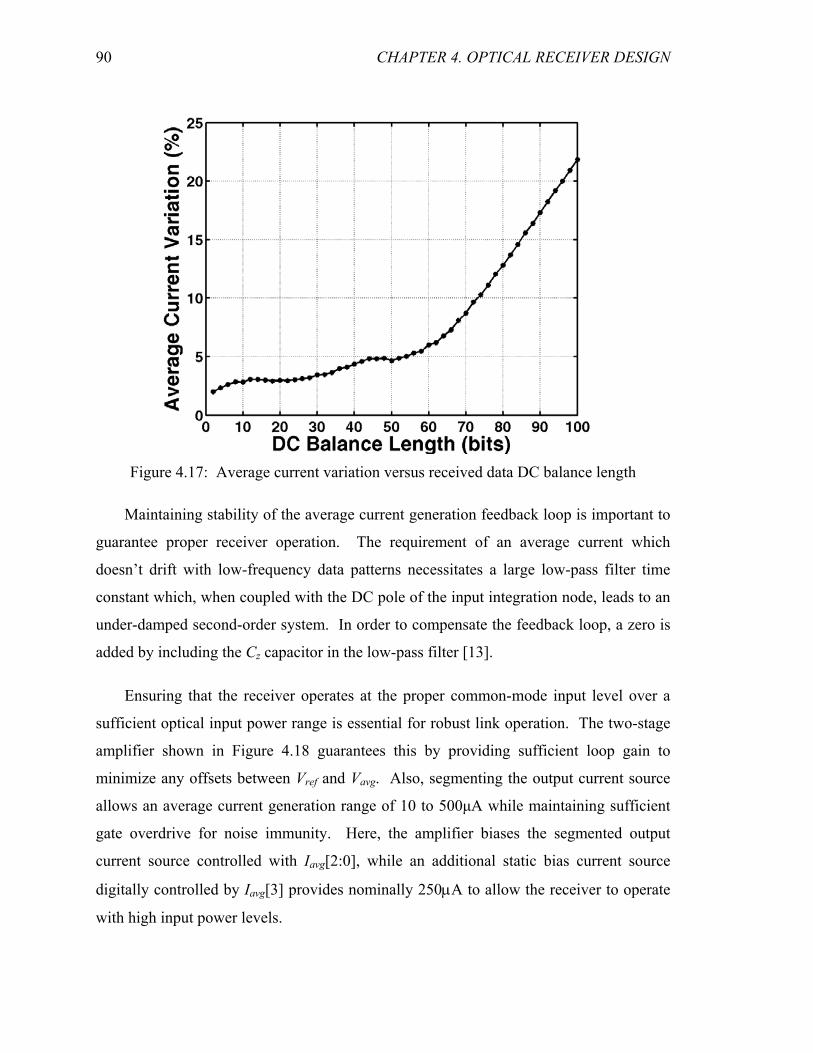
CHAPTER 4. OPTICAL RECEIVER DESIGN
90
Figure 4.17: Average current variation versus received data DC balance length
Maintaining stability of the average current generation feedback loop is important to
guarantee proper receiver operation. The requirement of an average current which
doesn’t drift with low-frequency data patterns necessitates a large low-pass filter time
constant which, when coupled with the DC pole of the input integration node, leads to an
under-damped second-order system. In order to compensate the feedback loop, a zero is
added by including the Cz capacitor in the low-pass filter [537H13].
Ensuring that the receiver operates at the proper common-mode input level over a
sufficient optical input power range is essential for robust link operation. The two-stage
amplifier shown in 538HFigure 4.18 guarantees this by providing sufficient loop gain to
minimize any offsets between Vref and Vavg. Also, segmenting the output current source
allows an average current generation range of 10 to 500μA while maintaining sufficient
gate overdrive for noise immunity. Here, the amplifier biases the segmented output
current source controlled with Iavg[2:0], while an additional static bias current source
digitally controlled by Iavg[3] provides nominally 250μA to allow the receiver to operate
with high input power levels.

CHAPTER 4. OPTICAL RECEIVER DESIGN
91
Figure 4.18: Average current generation feedback amplifier and segmented output current source
4.1.4 Receiver Performance Analysis
Receiver performance is ultimately measured by the bit-error-rate (BER). Link coupling
losses and limitations in the amount of transmit optical power place emphasis on
improving receiver sensitivity, which is defined as the minimum average received optical
power required to achieve a given BER [539H58]. Also relevant in the integrating receiver is
the amount of optical power that can be received before the input integrates beyond the
common-mode input level that ensures reliable data resolution. The ratio of this
maximum average optical power and the sensitivity form the receiver dynamic range,
which is important to maximize in order to guarantee receiver operation in systems where
both the coupling tolerances can vary and the optical power can degrade due to
component aging. This subsection discusses the parameters that comprise the integrating
receiver sensitivity and dynamic range and how these vary with data rate and frequency
content.
Due to the front-end’s integrating nature, the receiver sensitivity is a strong function
of the data rate, input capacitance, and photodiode responsivity, ρ [540H98]. Using Equation
541H(4.3) and the photodiode responsivity, the optical power swing, Pinpp, required to produce
a given voltage swing in one bit period is equal to
( )b
inpdbinpp T
CCVP
ρ+Δ
=2
. (4.8)

CHAPTER 4. OPTICAL RECEIVER DESIGN
92
Thus, receiver sensitivity for random NRZ data is
( )b
inpdbavg T
CCVP
ρ+Δ
= . (4.9)
Here Cin is equal to
sin nCCC 2int += , (4.10)
where Cint is the input interconnect capacitance, n is the demultiplexing factor (5), and Cs
is the total hold capacitance for each sampler. Note that while only half the samplers are
active at one time, Equation 542H(4.10) includes the factor of two Cs which accounts for the
equal number of phase samplers required for the clock recovery system discussed in
Chapter 5.
The required ΔVb is set by input referring the sum of the residual sense-amplifier
offset after correction, Voffset, and the voltage necessary for the sense-amplifier to
correctly resolve at a given data rate, Vmin. In addition, a minimum signal-to-noise ratio
(SNR) must be maintained in order to achieve a given BER and the interference
associated with the average current variation must be accounted. Combining these terms
results in a total minimum voltage swing per bit of
minVVSNRV offsetnb ++=Δ σ , (4.11)
where σ2n is the total input voltage noise variance which is computed by input referring
the receiver segment circuit noise and the effective clock jitter noise.
Contributing to the input referred circuit noise are the sense-amplifier, buffer, and
samplers in the receiver segments. The sense-amplifier is modeled as a sampler with
gain [543H98] and has an input referred voltage noise variance of

CHAPTER 4. OPTICAL RECEIVER DESIGN
93
Avsasa CA
kT2
2 2=σ .
(4.12)
Here CA is the internal sense-amplifier node capacitance which is set to approximately
40fF in order to obtain sufficient offset correction range. The sense-amplifier gain, Avsa,
is derived from Equation 544H(4.5) and is equal to near unity for the 0.9V common-mode
input level set by the buffer output, resulting in a sense-amplifier voltage noise sigma of
0.45mVrms. Buffer input referred voltage noise variance is a function of its gain, Avbuf,
and bandwidth, f3dB, and equal to
BWDmm
BWD
Dmvbuf
buf NRgg
kTNR
RgA
kT⎟⎟⎠
⎞⎜⎜⎝
⎛+=⎟⎟
⎠
⎞⎜⎜⎝
⎛+= 2
22
2 1818 γγσ ,(4.13)
where γ and gm are the input nMOS excess noise coefficient and transconductance, RD is
the resistor load, and NBW is the noise bandwidth for a single-pole amplifier equal to
dBBW fN 32π
= . (4.14)
The buffer power consumption is primarily set by noise constraints, as the near unity gain
and input demultiplexing ease the bandwidth requirements. A 250μA tail current
provides sufficient transistor transconductance to achieve a buffer voltage noise sigma of
1.03mVrms and a bandwidth of 14GHz. Sampler voltage noise variance is bandwidth
independent and equal to
ss C
kT22 =σ , (4.15)
where the factor of two is due to the receiver segments’ double-samplers which generate
the differential input voltage to the buffer. Here Cs is approximately 10fF, with 55% due
to the buffer input capacitance and 45% due to sampler and interconnect capacitance.
This results in an input sampler voltage noise sigma of 0.92mVrms.

CHAPTER 4. OPTICAL RECEIVER DESIGN
94
Clock jitter also has an impact on the receiver sensitivity because any deviations
from the ideal sampling time results in a reduced double-sampled differential voltage.
This timing inaccuracy is mapped into an effective voltage noise on the integrated input
signal with a variance of
22
2b
b
jclk V
TΔ⎟⎟
⎠
⎞⎜⎜⎝
⎛=
σσ ,
(4.16)
with the total clock jitter variance
222jTXjRXj σσσ += (4.17)
where σjRX and σjTX are the root-mean-square jitter of the receiver and transmitter clocks,
respectively. Proper clock generation and recovery techniques, explained in detail in
Chapter 5, are use to obtain a σj/Tb ratio of 4.3%. Assuming a nominal input voltage
swing of 15mV, this implies a clock jitter induced voltage noise sigma of 0.65mVrms.
Combining the input referred circuit noise and effective clock jitter noise,
2222clksbufsan σσσσσ +++= ,
(4.18)
results in a total input noise sigma of 1.59mVrms. The analysis in Section 545H4.1.2 shows
that Voffset can be reduced to 1.15mV and if coding is used to ensure proper data
frequency content, the average current variation is limited to less than 5%. Assuming
that Vmin is made negligible with adequate sense-amplifier regeneration time, a
ΔVb=11.9mV is required for a BER=10-10 (SNR=40.4).
The parameters shown in 546HTable 4.1 are used to compute the theoretical receiver
sensitivity shown in 547HFigure 1.1(a). The required optical power increases linearly with
data rate due to the integrating nature of the front-end, with a sensitivity of -9.8dBm at
10Gb/s.

CHAPTER 4. OPTICAL RECEIVER DESIGN
95
Table 4.1: Integrating receiver sensitivity parameters
ΔVb 11.9mV Cpd 220fF Input Capacitance
Cint 120fF Cs 10fF Total 220fF
ρ 0.5A/W
(a) (b)
Figure 4.19: Theoretical integrating receiver performance: (a) sensitivity versus data rate, (b) dynamic range versus DSV
While the sensitivity forms the lower bound of the receiver dynamic range, the upper
bound is set by the amount of optical power that can be received before the input
integrates beyond the common-mode input level that guarantees reliable data resolution.
This implies that the dynamic range is a function of the data frequency content, with
lower frequency data that has longer runlengths of consecutive bits constraining the
maximum power limit. One way to quantify the frequency content of a received data
sequence, d0…dn-1, is to compute the running disparity, Disp(d), which is a perpetual tally
of the number of zeros subtracted from the number of ones [548H21].
( ) ∑−
=
+−=1
02
n
iidnaDisp (4.19)

CHAPTER 4. OPTICAL RECEIVER DESIGN
96
The maximum variation in disparity, called the digital-sum variation (DSV), is the
effective number of bits that sets the integrating receiver input voltage swing. Thus, the
maximum voltage swing per bit is
DSVV
V range=max , (4.20)
where Vrange is the 500mV valid common-mode input range that is limited to a minimum
of 0.6V for sufficient sampler bandwidth and a maximum of 1.1V to prevent excessive
sampler leakage. The ratio of the minimum ΔVb and Vmax is equivalent to the receiver
dynamic range
minmin
max
min
max
b
range
b VDSVV
VV
PP
DRΔ
=Δ
== , (4.21)
which is plotted in 549HFigure 1.1(b). A dynamic range of 8.45dB is achieved if the receiver
is used in a system with 8B10B encoded data which has a DSV equal to 6bits [108F109].
4.2 Input Swing Control Filter
The previous section detailed the design of a low-voltage integrating and double-
sampling receiver front-end that achieves adequate sensitivity and dynamic range for
systems where a coding scheme, such as 8B10B, is employed. While 8B10B coding is
very popular, some systems are unwilling to pay the 25% coding overhead and thus
implement codes with higher DSV values. The resulting impact on achievable dynamic
range is a major constraint for the use of the integrating optical receiver in these systems
with significant low-frequency data content.
This section discusses the addition of a swing control filter that potentially allows for
the resolution of uncoded data. First, is an overview of how the filter actively clamps the
input signal within the receiver input range. Next is a discussion of the key circuits that
comprise the swing control filter. The section concludes with an overview of the key
performance issues, including noise, circuit offsets, and timing skew.

CHAPTER 4. OPTICAL RECEIVER DESIGN
97
4.2.1 Swing Control Filter Overview
As the front-end integrates the photodiode current on the receiver input node, there is the
potential to exceed the common-mode input level that guarantees reliable data resolution
due to the excessive amount of charge imbalance introduced by data sequences with high
DSV values. In order to prevent receiver saturation, it is conceivable to reset the input
node to the middle of the common-mode range by either supplying or depleting an equal
magnitude of charge with the opposite polarity introduced by the input signal during the
previous bit time. Ideally, this charge balancing occurs a short instance after the received
bit, such that the impact on the next bit is minimized. This creates an effective integrate
and dump receiver, as shown in 550HFigure 4.20.
Tb
Vb
V0
V1
V0 < V1 D[0]=1Vin
time
D[0]D[-1] D[1] D[2]ReceivedData
integrate
dump
ResetPulse
Figure 4.20: Integrate and dump receiver
However many limitations exist in implementing an integrate and dump receiver at
high data rates, including sampling the input voltage at the proper times, producing the
narrow reset pulses, and injecting an accurate amount of charge in a small fraction of a
bit period. Thus, it was proposed by Emami [109F110] to introduce this balancing charge at
the same rate of the incoming charge by adding additional synchronized switched current
sources controlled with previous data bits, as shown in 551HFigure 4.21(a). The switched

CHAPTER 4. OPTICAL RECEIVER DESIGN
98
current sources’ value is set such that, when combined with the average current source,
the net current delivered to the input node is either I1 or I0. While this is the most
intuitive way to alter the original integrating front-end to perform the input charge
balancing, unfortunately the difficulty of synchronizing, lack of voltage headroom, and
the additional loading associated with two additional switched current sources make this
implementation impractical. Thus, this idea is augmented by changing the static current
source value from Iavg to I0 and using only a single switched current source that sinks a
current of IΔ, as shown in 552HFigure 4.21(b). This modification results in the input current
source exactly mimicking the photodiode operation by constantly sinking from the input
node a value of I0 and switching a current of IΔ based on previously received data bits.
While the static current source value is altered from Iavg to I0, it will be shown that the
bias generation filter is unchanged due to the interaction between the switched current
source and input signal and also the fact that the static current source bias generation
filter is acting to force the input voltage to the middle of the common-mode range.
The input node response to a repeating 20 bit data pattern is shown in 553HFigure 4.22 to
illustrate how the input dynamics have changed with the now I0 static current source and
the addition of the switched IΔ current source. Assuming synchronization of the switched
current source with the input signal, the net integration current is now
( )
0 ,1 ; ;0
1 ,0 ;
0
0
0
0
===
==
==−=
+−=
−Δ
−
−Δ
−Δ
LD
LD
LD
LDinnet
ddIdd
ddIzIIII
, (4.22)
where LD is the feedback loop delay from the time a bit is received to when the bit
controls the switched current source. When the incoming data bit, d0, and the feedback
bit, d-LD, are unequal, the input voltage will now swing twice the ΔVb value of the original
integrating receiver, as now a full IΔ integrates on the input node versus IΔ/2 from
Equation554H(4.3). While when the incoming data bit and the feedback bit are equal, the
input voltage will remain constant, as the net integration current is zero. Also, most
importantly, the input voltage is now clamped to swing a maximum number of bits equal

CHAPTER 4. OPTICAL RECEIVER DESIGN
99
to the feedback loop delay and independent of the received data DSV. Thus, the added
circuitry is referred to as a swing control filter (SCF). Now, the receiver dynamic range
with the SCF becomes
( )min2 b
range
VLDV
DRΔ
= . (4.23)
(a)
(b)
Figure 4.21: Input node of modified integrating receiver with added switched current sources that form the swing control filter: (a) original proposition [555H110], (b) transformed for practical implementation

CHAPTER 4. OPTICAL RECEIVER DESIGN
100
While increased input demultiplexing allows operation at higher data rates, it also
implies increased loop delay relative to the bit time, with six bits required in the
implemented 1:5 input demultiplexing receiver operating at a minimum 2FO4 bit period.
This results in a maximum input voltage swing of 12ΔVb relative to the original
integrating receiver. Because the input now has twice the voltage swing for unequal
incoming data and feedback bits, the dynamic range is actually 3dB (optical power)
worse than the original integrating receiver for data with DSV less than or equal to the
feedback loop delay, as shown in 556HFigure 4.23. However, once the DSV exceeds the loop
delay, the dynamic range with the swing control filter clamps at 5.4dB. This allows for
dynamic range improvement once the DSV exceeds twice the loop delay value.
Figure 4.22: Input voltage, net current, and dynamic offset values for the integrating receiver with swing control filter (LD=6bits)

CHAPTER 4. OPTICAL RECEIVER DESIGN
101
Figure 4.23: Theoretical integrating receiver dynamic range versus DSV with and without swing control filter
Since the input swing is now clamped inside the desired common-mode input range,
there is an issue in resolving the data when the incoming bit is equal to the feedback bit
and there is no net voltage swing. However, because the feedback data is known, the
effect the switched current source has on the input voltage can be predicted and
compensated for by adjusting the sense-amplifier offset settings. Thus, in order to
resolve the incoming data, a dynamic offset voltage controlled by the feedback data value
adapts the sense-amplifier threshold voltage. For the four possible combinations of input
and feedback data values, an optimally set threshold of ±ΔVb provides a net voltage
margin of ΔVb equivalent to the original integrating receiver front-end margin.
4.2.2 Swing Control Filter Circuits
Several key circuit additions are necessary to augment the original integrating receiver
front-end to include the swing control filter, as shown in 557HFigure 4.24. Now at the
receiver input there are two current sources that balance the photodiode current, the I0
source that is set by the same low-pass filter as in the original integrating receiver
implementation and the switched IΔ source controlled by the feedback data values. This
subsection begins by describing the design of the switched IΔ current source operating at
the full data rate. Next, the control loop that sets the IΔ current value and forces the static

CHAPTER 4. OPTICAL RECEIVER DESIGN
102
current source to adjust from Iavg to I0 is detailed. Finally, the technique used to
dynamically adjust the sense-amplifier threshold is discussed.
Figure 4.24: Integrating receiver with swing control filter
Switched IΔ Current Source The switched IΔ current source must deliver an accurate current value at the full data rate
with minimum latency in order to reduce the overall feedback loop delay. Here, as in the
optical transmitter designs, the same challenge of performing high-speed parallel data
multiplexing is faced. Thus, the same multiple clock phase multiplexing technique used
in the optical transmitters is applied here, as shown in 558HFigure 4.25. However in order to
minimize loop delay, now the multiplexing and current steering functions are combined
with a fully differential multiplexer that steers the IΔ tail current between the receiver
input node and a dummy load.
It is important that the switched current source is synchronized with the input
samplers for proper operation. In order to guarantee this, the same clock phases used to
generate the sample signals are used to switch the IΔ current source. A current pulse is
initiated in each of the five two-transistor multiplexing segments by switching on the top
transistor controlled with the rising edge of the same signal used for input sampling,
samp[n]. Data qualification and current pulse termination is performed with the bottom
transistor control signal, dclk[n], which ideally coincides with the rising edge of

CHAPTER 4. OPTICAL RECEIVER DESIGN
103
samp[n+1]. While the same OR function that generates the sampling signals cannot be
used to control the bottom multiplexing transistor due to the necessary data qualification,
with proper design the skew between dclk[n] and samp[n+1] is minimized to a small
fraction of a bit period.
d [n]D[n-LD][n+1]
samp[n]
I
[n+1][n]
D[n-LD][n+1]
samp[n]
d [n]
Vin I +
samp[n]
d [n]
I + D[n-LD] D[n-LD+1]D[n-LD-1]
Mux Waveforms
V
Figure 4.25: Switched IΔ current source
IΔ and I0 Current Generation The IΔ current value is dynamically adjusted with a control loop, shown in 559HFigure 4.24, in
order to track fluctuations in the incoming data power level. If the IΔ current is properly
set, there should be no net voltage swing at the input when the incoming and feedback
data bits are equal. The control loop works by inserting an additional receiver segment to
monitor this. Information from this additional receiver segment is fed to logic controlling
a charge-pump that integrates charge on a capacitor to set the IΔ bias voltage. Note that
the comparator in this receiver segment has static settings to cancel the input referred
offset, as opposed to the dynamic offset settings used in the other data receiver segments.
Previously, the low-pass filter setting the input common-mode voltage biased the
static current source equal to the average input photocurrent, Iavg. However, now the low-
pass bias filter adjusts the static current source to supply the difference between Iavg and
the average current from the switched IΔ current source (IΔ/2), which is a net result of I0.
This is verified in the simulation result of 560HFigure 4.26, where the switched IΔ current

CHAPTER 4. OPTICAL RECEIVER DESIGN
104
source is initially disabled and the static current source converges to the average
photocurrent with I0=30μA and I1=140μA. After the initial 10kbits, the IΔ control loop is
enabled and both the IΔ and the static current sources converge to the correct values.
Figure 4.26: I0 and IΔ control loop locking behavior; I0=30μA, I1=140μA, IΔ=110μA
Because only slow fluctuations in the incoming data power level are expected, the
nominal bandwidth of the IΔ control loop is set roughly an order of magnitude lower than
the static current source bias generation filter. This low loop bandwidth is set in an area-
efficient manner with a programmable 4-bit counter in the control logic that acts as a
digital low-pass filter. Digital filtering allows the IΔ loop dynamics to remain constant
when operating at different data rates.
Dynamic Offset Voltage Generation In order to provide a net ΔVb voltage margin equivalent to the original integrating
receiver case, the receiver segments’ threshold must be dynamically adjusted between
±ΔVb as a function of the feedback data. This dynamic threshold is implemented in the
same manner as the normal receiver segment offset cancellation by adjusting the internal
sense-amplifier node capacitance, as shown in 561HFigure 4.27. For each receiver segment,
two 10-bit Offset codes are used that are pre-calibrated to the nominal “zero” offset value
±ΔVb. These two 10-bit codes are the inputs to a 2-to-1 multiplexer that uses the
feedback data bit as the select signal. This mux select signal is latched with the inverted

CHAPTER 4. OPTICAL RECEIVER DESIGN
105
sense-amplifier evaluate clock in order to guarantee transitioning only while the sense-
amplifier is in pre-charge mode.
Figure 4.27: Sense-amplifier dynamic offset generation
While this approach requires pre-calibration, the same hardware could be used in an
automated control loop. One potential automated approach to offset generation is to add
another control loop that includes an additional receiver segment whose offset value is
adjusted periodically to be equal to zero or the 2ΔVb swing that occurs with the addition
of the swing control filter. The difference between these two offset codes divided by two
could then be used in the other main data receiver segments as the delta from the nominal
zero offset settings, provided there exists sufficient linearity and lsb matching between
the offset correction DACs.
4.2.3 Swing Control Filter Performance Issues
The potential dynamic range performance gain with the added swing control filter is a
strong function of the feedback data loop delay. This critical path, formed by the
feedback to the switched current source, is shown in 562HFigure 4.28. Starting loop delay
calculation at the rising edge of samp[0], one bit period is used to integrate the incoming
data bit, d0. Another bit period is budgeted after integration for the differential buffer to
adequately settle before the sense-amplifier begins to evaluate. From 563HFigure 4.7, the

CHAPTER 4. OPTICAL RECEIVER DESIGN
106
sense-amplifier requires approximately 4FO4 to regenerate the input sufficiently enough
to switch the RS latch. Next, the propagation through the RS latch and IΔ switched
current source predriver is approximately 2.5FO4. This results in a total loop delay of
2bits plus 6.5FO4, which at a minimum 2FO4 bit period is equal to 5.25bits. In order to
provide robust operation, this tally is rounded up to an integer value of 6bits. Note that at
less aggressive data rates further improvement in the dynamic range is possible. For
example, a 3.3FO4 bit period, which is approximately 10Gb/s in the 1V 90nm CMOS
technology of implementation, reduces the loop delay to 4bits and increases the minimum
dynamic range from 5.4dB to 7.2dB.
Figure 4.28: Swing control filter critical path
It is important to effectively deal with input noise and offset to ensure proper swing
control filter performance. Any residual input-referred offset in the receiver segment
monitoring the IΔ magnitude reflects directly into offset on the IΔ source, as shown in
564HFigure 4.29. Here a 20% ΔVb offset in the IΔ receiver segment causes the IΔ source to
lock onto a value 20% lower than the 110μA nominal value. The static current bias filter

CHAPTER 4. OPTICAL RECEIVER DESIGN
107
then compensates this IΔ offset by adjusting the static current source away from the 30μA
I0 value. In order to minimize this issue, the offset correction circuitry can reduce Voffset
to 1.15mV, as discussed in Section 565H4.1.2 . After the currents have settled to their steady-
state values, the IΔ receiver segment samples a very small signal. Thus, without proper
filtering, input noise can cause incorrect decisions that result in ripples in the IΔ and static
current source values. The magnitude of the noise-induced ripples is minimized by
increasing the counter value of the digital filter in the IΔ control logic and using a small
charge pump current of approximately 10μA.
Figure 4.29: I0 and IΔ control loop locking behavior with 20% ΔVb offset and σn=13% ΔVb; I0=30μA, I1=140μA, IΔ=110μA
Another swing control filter performance issue is the required synchronization of the
switched IΔ current source with the input photocurrent signal. As shown in 566HFigure 4.30,
interference will occur in bits that neighbor an IΔ transition if a phase error is present in
the IΔ switched current timing. This synchronization error can have a dramatic effect, as
the IΔ current source transitioning early by 20% of a bit period causes a 20% voltage error
relative to the 2ΔVb swing. With the dynamic ΔVb offset present in the data receiver
segments, this results in a 40% degradation of the net voltage margin. Due to the
importance of minimizing the IΔ timing error, the same samp[n] signals used to sample
the input waveform are used to control the switched IΔ current source.

CHAPTER 4. OPTICAL RECEIVER DESIGN
108
Figure 4.30: IΔ phase error effect on input voltage waveform
4.3 Experimental Results
In order to investigate the performance of the proposed integrating receiver architectures,
two versions of the receiver with a 1:5 demultiplexing factor were designed in a 1V 90nm
CMOS technology as part of an optical transceiver test-chip shown in 567HFigure 4.31. The
first receiver implementation is the baseline integrating and double-sampling architecture
modified for low-voltage operation, while the second design expands upon this with the
inclusion of the swing control filter.
568HFigure 4.32 shows the optical test setup, with the VCSEL transmitter from Chapter 3
used to generate the high-speed optical data signal, thereby forming a complete optical
link. 850nm photodiodes, with measured 0.5mA/mW responsivity, are mounted directly
on the CMOS chip and attached with short wirebonds. The VCSEL output beam is free-
space imaged to the receiver board and focused on a photodiode via a system of lenses.
Proper operation of the low-voltage integrating and double-sampling receiver is verified
by observing the receiver input integrating node response to a 10Gb/s 20bit repeating
data pattern obtained with on-die subsamplers, shown in 569HFigure 4.33.

CHAPTER 4. OPTICAL RECEIVER DESIGN
109
Figure 4.31: 850nm photodiodes wirebonded to optical receivers
Figure 4.32: Optical link test setup
Receiver sensitivity, plotted in 570HFigure 4.34, was measured for both 8B/10B data
patterns and also longer runlength data with a maximum variance of 10bits in order to
further stress the integrating receiver. Due to the integrating nature of the front-end, the

CHAPTER 4. OPTICAL RECEIVER DESIGN
110
required optical power increases roughly linearly from 5 to 14Gb/s, with a sensitivity of
-9.6dBm at 10Gb/s for a BER of 10-10. These results correlate with the predicted
theoretical sensitivity up to about 14Gb/s. At higher data rates, the required optical
power increases at a greater rate primarily due to increased ISI and jitter from reflections
associated with the photodiode wirebond connection, as shown in the simulation results
of 571HFigure 4.35. The sensitivity at the maximum data rate of 16Gb/s is -5.4dBm. It is
worth noting that with a more integrated approach, such as flip-chip bonding the
photodiodes, superior sensitivity numbers could be achieved due to the minimization of
the inductive bondwire parasitics.
Figure 4.33: Integrating receiver input node response to a 10Gb/s 20bit repeating pattern. Note from the on-die measurement, bits 3 and 13 are somewhat distorted due to periodic noise on the subsamplers supply that is believed to not be present on the input waveform.

CHAPTER 4. OPTICAL RECEIVER DESIGN
111
Figure 4.34: Measured integrating receiver sensitivity versus data rate
(a) (b)
Figure 4.35: Simulated impact of photodiode wirebond connection on the receiver’s sampled differential input voltage at 16Gb/s: (a) no bondwire, (b) 0.3nH bondwire
Operation of the integrating receiver with the added swing control filter is verified by
observing the receiver input integrating node response to the same 10Gb/s 20bit repeating
data pattern, shown in the subsampled waveform of 572HFigure 4.36. The integrated
waveform is now clamped with the swing control filter activated, as predicted in 573HFigure
4.22, and the correct data is resolved with the proper dynamic offset settings. While

CHAPTER 4. OPTICAL RECEIVER DESIGN
112
resolution of certain 20bit patterns was achieved with the swing control filter activated,
unfortunately verification of robust receiver operation was not obtained due to both phase
errors between the switched IΔ current source and feedback error propagation.
The synchronization errors form ripples in the ideally flat part of the subsampled
waveform, reducing the double-sampled voltage margin, and potentially leading to data
resolution errors. Because the signals controlling the input samplers and the switched IΔ
current source are generated from common clock signals, ideally there exists minimal
phase error. However, when systematic layout and random mismatches are factored in,
there is the potential for the delay error between the NAND and NOR gates used in the IΔ
current source predrive and the extra delay of the current source to be magnified. These
phase errors could potentially be minimized in future implementations with independent
phase adjustment between the input samplers and the switched IΔ current source.
Another issue occurs with repeating data patterns, where there is the potential for
errors to propagate in a positive feedback manner and cause the IΔ current generation
loop to lock onto incorrect values. This is exasperated by the fact that the current
implementation of the IΔ current generation loop only potentially receives updates one
out of every five bits, and thus there is not enough information to break error
propagation. Potential solutions to this problem are either increasing the number of
additional receiver segments that supply information to the IΔ control logic or potentially
using a known test pattern to initially set and lock the current values.
574HTable 4.2 summarizes the optical receiver performance. The integrating and double-
sampling receiver total power dissipation is 23mW at 16Gb/s. Power increases to 26mW
when the swing control filter is added due to the extra receiver segment and the switched
IΔ current source. The receiver front-end (excluding CDR) occupies a total area of
0.025mm2, which increases to 0.028mm2 with the addition of the swing control filter.

CHAPTER 4. OPTICAL RECEIVER DESIGN
113
Figure 4.36: Integrating receiver with swing control filter input node response to a 10Gb/s 20bit repeating pattern. Note the voltage ripples in the ideally flat part of the input waveform due to a phase error in the IΔ current source, similar to the simulation results of 575HFigure 4.30.
Table 4.2: Optical receiver performance summary
Technology 90nm Standard CMOS Power Supplies / Threshold Vdd=1V, PDBias=2.5V, Vth~0.35V Data Rate 5-16Gbps Input Capacitance
Photodetector 220fF Circuitry/Wiring 220fF Total 440fF
Sensitivity (BER<10-10) (Voltage, Current, Optical Power) 10Gb/s 12.5mV, 110μA, 220μWpp (-9.6dBm) 16Gb/s 20.2mV, 284μA, 569μWpp (-5.4dBm)
Power @ 16Gb/s Int. RX Front-End 23mW (1.4mW/Gb/s) Int. RX + SCF 26mW (1.6mW/Gb/s)
Area Int. RX Front-End 0.025mm2 Int. RX + SCF 0.028mm2

CHAPTER 4. OPTICAL RECEIVER DESIGN
114
4.4 Summary
Optical receivers are required to convert a small amount of optical power to an electrical
signal and amplify it into a logic-level voltage. Unfortunately, the reduced voltage
headroom and intrinsic device gain associated with CMOS process scaling has degraded
the ability to efficiently achieve this goal with linear transimpedance and limiting
amplifiers. Thus, to enable high-speed, dense optical receivers that are compatible with
current and future CMOS processes, this chapter presented a low-voltage integrating and
double-sampling receiver front-end that eliminates linear high-gain elements operating at
the full data rate.
Modifications were discussed that enable low-voltage operation and improved
uncoded data dynamic range performance relative to Emami’s original integrating and
double-sampling optical receiver. Adding a low-power buffer in the receiver segments
after the input demultiplexing allows a 500mV common-mode input range in a 1V
process by fixing the sense-amplifier common-mode input level for improved speed and
offset performance and also reducing kickback charge. Dynamic range enhancement for
data with high DSV is achieved by augmenting the receiver to include a swing control
filter which actively clamps the input signal within the input range and employs dynamic
threshold adjustment for data resolution.
Optical receiver operation is achieved at bit periods as low as 2FO4 at a low-power
consumption of 1.4mW/Gb/s without the use of any high-area passives. While
performance improvements are still necessary for robust swing control filter operation,
the technique shows a potential path for the integrating receiver in systems that cannot
afford large coding overheads.

115
Chapter 5 Clock Generation and Recovery
The previous two chapters discussed optical transmitter and receiver circuits that achieve
high data rate operation and good energy efficiency by employing time-division
(de)multiplexing architectures. These designs rely upon low-noise clocks with high-
precision phase spacing to guarantee sufficient link timing margins. This chapter looks at
power and area-efficient circuits used for clock generation, distribution, and performing
timing recovery at the receiver.
Having a general purpose link cell with the flexibility to operate over a wide range of
data rates is desirable due to the large number of high-speed I/O standards which differ in
their data transfer demands. This requires clock generation in a manner that guarantees
optimal performance over a wide frequency range and is also robust to variations in
process, voltage, and temperature. Adaptive-bandwidth clock synthesis architectures,
which scale system dynamics in proportion with operating frequency, efficiently achieve
this goal.
System flexibility also requires power-efficient timing recovery at the receiver in
order to phase align the clocks to the optimal data sampling time due to the incoming data
phase varying with different system channels. This task is complicated by the presence
of both receiver oscillator and input timing noise, which must be suppressed in

CHAPTER 5. CLOCK GENERATION AND RECOVERY
116
conflicting manners. A conventional dual-loop clock and data recovery (CDR) system
[576H25], with a frequency synthesis loop and a secondary phase interpolating loop, can
achieve high performance due to the freedom to optimize both the frequency synthesis
loop bandwidth to filter VCO jitter and the phase loop bandwidth to reduce jitter transfer
from the noisy input signal. However, implementing a straight dual-loop CDR in an
input demultiplexing receiver is costly in terms of area and power, as the required
circuitry grows with the demultiplexing factor.
Another important clocking issue involves guaranteeing precise clock phase spacing
at the critical points of transmitter multiplexing and receiver demultiplexing. While
CMOS scaling allows for smaller, faster, and lower power circuitry, unfortunately scaling
degrades the matching that is required to provide uniform clock phases. Phase errors,
caused by both systematic loading imbalances and random mismatches in the VCO,
distribution buffers, and interconnect, degrade the link timing margin and necessitate the
use of efficient phase correction circuitry.
This chapter describes the circuitry that produces the low-noise clocks with high-
precision phase spacing that are used by the (de)multiplexing receiver and transmitter.
The chapter begins with an overview of the frequency synthesis PLL capable of scaling
loop dynamics for optimal performance over a wide frequency range. Next is a
presentation of the dual-loop clock recovery system which employs baud-rate phase
detection and feedback interpolation to achieve reduced power consumption. A
discussion of the delay adjustment circuitry which is applied independently to transmit
and receive clocks on a per-phase basis in order to tune out static phase errors follows.
Finally the chapter concludes with experimental results of the frequency synthesis PLL
and the clock recovery system.
5.1 Clock Generation
In order to enable data rate flexibility in a general purpose I/O cell, it is necessary for the
clocking circuitry to maintain adequate performance over the entire frequency range of
interest. PLL jitter performance and stability are governed by its system dynamics,

CHAPTER 5. CLOCK GENERATION AND RECOVERY
117
which are often quantified by the loop bandwidth ωn and damping factor ζ. In order to
obtain optimal jitter performance, it is often necessary to set the loop bandwidth to be a
constant fraction of the PLL reference clock.
One efficient manner to achieve this is with self-biasing techniques proposed by
Maneatis [577H32] which use the VCO control voltage to both bias the charge-pump current
and also adjust the effective filter resistance. Sidiropoulos expands this technique to
PLLs with supply-regulated VCOs [578H33] which are better suited for low-voltage operation.
These self-biasing techniques are applied to the circuit blocks of the implemented clock
generation PLL in order to achieve the adaptive bandwidth criteria.
5.1.1 PLL Circuits
579HFigure 5.1 shows the circuit blocks of the clock generation PLL, which employs a
voltage-controlled ring oscillator to produce the multiple clock phases used in data
multiplexing. A linear regulator supplies power to the VCO and also sets the oscillation
frequency by buffering the control voltage, VCTRL, produced by the interaction between
the phase-frequency detector, charge-pump, and loop filter. VCTRL is also used to both
bias the charge-pump current and adjust the effective filter resistance in order to achieve
the adaptive bandwidth PLL criteria. The following subsections discuss the design of the
loop components.
PFD CPVCTRL
bias
biasref clkup
dn
C
VCO
CDEC
Multiphase Clocks
N
VREG
fb clk
Figure 5.1: Clock generation PLL

CHAPTER 5. CLOCK GENERATION AND RECOVERY
118
Voltage-Controlled Oscillator In order to generate the five sets of complementary clock phases required by the
multiplexing transmitter, the ring oscillator shown in 580HFigure 5.2 is used [581H29]. This
oscillator’s CMOS inverter-based delay elements allows for low-voltage operation and
also enables easy portability between different process technologies. Because a single-
ended ring oscillator cannot provide complementary clock phases, two oscillator stages
are coupled with inverters connected between the two rings. Higher oscillation
frequencies are achieved by connecting the coupling inverters in a forward interpolation
manner [110F111].
Figure 5.2: Coupled ring oscillator [582H29]
The oscillation period is set by the VCO’s regulated supply voltage (ideally VCTRL)
and is proportional to the delay element output time constant TD2F
3
( )thCTRLVCO
VCOeffDeffVCO VV
CnTnT
−=∝
β2
2 , (5.1)
3 Here the output time constant is assumed to be the product of the delay stage load capacitance and the “on resistance” of a linear MOSFET, as in [33].

CHAPTER 5. CLOCK GENERATION AND RECOVERY
119
where neff is the effective number of delay elements in the ring3F
4, CVCO is the delay stage
load capacitance, and βVCO and Vth are the fitted transconductance factor and threshold
voltage of the VCO transistors. Thus, the VCO gain is
VCOeff
VCO
CTRL
VCOVCO CnV
fK
2β
=∂∂
= (5.2)
and is approximately 8.6GHz/V in the 90nm CMOS technology of implementation.
Voltage Regulator A voltage regulator, shown in 583HFigure 5.3, is required to power the VCO since the loop
filter cannot supply the required amount of oscillator switching current. In order to set
the VCO supply to a voltage approximately equal to VCTRL, a unity-gain feedback
configuration is formed with a differential amplifier driving the output pMOS current
source. High-frequency switching noise from the oscillator is filtered with a large
decoupling capacitor placed at the regulator output.
Figure 5.3: Linear regulator for VCO supply filtering
Compensation is necessary to ensure regulator stability due to the presence of two
poles from the differential amplifier and the filtered regulator output. Also, the regulator
bandwidth must be sufficient enough to not affect the overall loop dynamics. In the
implemented design, the regulator’s dominant pole is formed with the large decoupling 4 The use of forward interpolation in the ring oscillator reduces neff from 5 to near 3.75.

CHAPTER 5. CLOCK GENERATION AND RECOVERY
120
capacitor (CDEC~20pF) placed at the VCO supply. The differential amplifier is self-
biased to track the VCO current draw and set the total regulator bandwidth to roughly ten
times the PLL loop bandwidth. This allows for constant loop dynamics, reduced power
consumption at lower data rates, and reduced voltage offsets. While Miller compensation
could potentially reduce the required compensation capacitance area [111F112], this comes at
the cost of reduced supply noise rejection. Another proposed technique is the used of
replica feedback compensation [112F113], which relaxes the trade-off between amplifier
bandwidth and supply rejection.
Phase-Frequency Detector, Charge-Pump, and Loop Filter A common phase-frequency detector [113F114], shown in 584HFigure 5.4, is used in the PLL in
order to provide a wide frequency capture range. This PFD uses NAND-based latches
that provide sufficient state elements to detect cycle slipping and prevent locking on
undesired harmonics. While there are faster PFDs, analyzed in [114F115], the implemented
design was fast enough for sufficient operation with the minimum 10FO4 clock period
and was chosen for its robustness and ease of portability.
Figure 5.4: Clock generation PLL phase-frequency detector

CHAPTER 5. CLOCK GENERATION AND RECOVERY
121
The PFD produces the control signals up and dn which switch the charge-pump,
shown in 585HFigure 5.5. Charge-pump current ICP is sourced or sunk from the series RC
loop filter for the phase error duration. The charge-pump current is self-biased with the
VCO control voltage, such that
( )2thCTRLCPCP VVI −= β . (5.3)
Using Equation 586H(5.1), once the PLL is in a locked state the reference frequency is
( )VCOeff
thCTRLVCOVCOref CNn
VVN
−==
πβωω , (5.4)
and this charge-pump biasing allows
⎟⎠⎞
⎜⎝⎛
⎟⎟⎠
⎞⎜⎜⎝
⎛==
CCNn
NCKIN VCO
VCO
CPeff
VCOCP
VCOref
n
ββ
πωωω
21
. (5.5)
Thus, the loop bandwidth is now a stable fraction of the reference frequency set by the
ratios of charge-pump to VCO transistor transconductance factors and VCO stage
capacitance to loop filter capacitance.
Figure 5.5: Charge-pump and loop filter

CHAPTER 5. CLOCK GENERATION AND RECOVERY
122
587HFigure 5.5 shows the series RC loop filter, where the resistor is implemented by a
pMOS transistor operating in the linear region. Grounding the pMOS transistor’s gate
results in an effective resistance of
( )thCTRLR VVR
−=
β1
. (5.6)
This results in
⎟⎟⎠
⎞⎜⎜⎝
⎛⎟⎟⎠
⎞⎜⎜⎝
⎛==
VCOR
VCOCP
eff
n
CC
NnRC 2
122
12 β
ββωζ ,
(5.7)
with the damping factor now a constant determined by the transconductance ratio of the
key transistors in the charge-pump, VCO, and filter resistor and also the ratio of the filter
capacitance to the VCO stage capacitance. Thus, these self-biasing techniques satisfy the
adaptive bandwidth requirements that enable both a fixed ratio between loop bandwidth
and reference frequency and also a constant damping factor.
5.2 Clock Recovery
The previous section detailed the design of an adaptive-bandwidth PLL used to generate
multiple clock phases that serialize data at the transmitter and deserialize data at the
receiver. While in the transmitter case common clocks are used for both data generation
and multiplexing, at the receiver a clock and data recovery system is necessary due to the
phase of the incoming data being initially unknown and potentially varying with
operating conditions. In order to provide sufficient timing margins, the CDR must
suppress both receiver oscillator noise and input data timing noise, which have
conflicting filtering requirements. Also, the CDR must be implemented in a power and
area-efficient manner.
This section discusses a dual-loop clock recovery system which allows for optimal
filtering of both local oscillator noise and input data timing noise. First, an overview of

CHAPTER 5. CLOCK GENERATION AND RECOVERY
123
the reduced power baud-rate phase detection method is given. An outline of the
performance, power, and area trade-offs between potential dual-loop implementations
follows. Finally, the section concludes with the details of the reduced power and area
dual-loop CDR with feedback interpolation.
5.2.1 Phase Detection
A CDR’s phase detector extracts phase information from the incoming data signal and
provides correction signals to circuitry which adjusts the receiver clocks phase position.
In order to minimize timing offsets, a phase detector consisting of the main data receiver
segments and identical phase receiver segments is implemented, shown in 588HFigure 5.6.
The received data DRX[n] and the phase values Ph[n] are processed by the phase logic to
produce a digital output signal which indicates whether the clock signals are sampling
early or late. This digital, or bangbang, control signal is then used to adjust the receiver
clocks to their optimal sampling position. The following subsection discusses the trade-
offs between a 2x-oversampling and a baud-rate phase detector.
Figure 5.6: CDR bangbang phase detector
2x-oversampling, outlined in 589HFigure 5.7, is a common phase detection technique
used in electrical links and was modified for the integrating receiver front-end by Emami
[590H98]. This method samples the input voltage with “quadrature” clocks ΦQ[n] ideally

CHAPTER 5. CLOCK GENERATION AND RECOVERY
124
spaced one-half of a bit period from the main data sampling clocks Φ[n]. Similar to data
detection, digital phase information signals Ph[n] are obtained by comparing consecutive
phase samples, Vpn and Vpn+1. Valid phase information is extracted for two-bit patterns
that contain a transition, with an “early” vote when Ph[n] is equal to DRX[n] and a “late”
vote when Ph[n] is opposite to DRX[n]. As shown in the phase detector simulation results
in 591HFigure 5.8, this results in a 50% phase update probability for random data input. While
this technique is very robust, generating and distributing the quadrature clocks results in
both power and area overheads [592H110].
Figure 5.7: Input voltage waveform with 2x-oversampling phase detection [593H98]
Figure 5.8: Phase update probability for 2x-oversampling and baud-rate phase detection
Baud-rate phase detection, proposed in [594H98] and outlined in 595HFigure 5.9, requires no
additional clock phases. Unlike 2x-oversampling phase detection, the baud-rate

CHAPTER 5. CLOCK GENERATION AND RECOVERY
125
technique uses the same data detection samples for phase detection, with a digital phase
signal Ph[n] produced by comparing samples separated by two bit periods, Vn and Vn+2.
Valid phase information is extracted for certain four-bit patterns that contain a middle
transition and a maximum of one additional transition, as outlined in 596HTable 5.1. As in the
2x-oversampling case, an “early” vote is registered when Ph[n] is equal to DRX[n] and a
“late” vote when Ph[n] is opposite to DRX[n]. However, not all four-bit data patterns in
597HTable 5.1 have complete phase information, as shown in the lower-right example of
598HFigure 5.9. Here a “late” vote cannot be reliably resolved due to ideally no voltage
differential between Vn and Vn+2, which in the presence of input noise also results in a
25% probability of erroneous “early” updates when the clock signals are actually late.
Thus, out of the 16 possible four-bit data patterns, two give complete phase information
and four give phase information in one direction with a 25% erroneous probability. This
results in a 25% correct and 6.25% incorrect update rate, for a net phase update
probability of 18.75% with random input data, as verified in the simulation results of
599HFigure 5.8.
Figure 5.9: Input voltage waveform with baud-rate phase detection [600H98]

CHAPTER 5. CLOCK GENERATION AND RECOVERY
126
Table 5.1: Data patterns with phase information for baud-rate phase detection
Pattern late early 25% erroneous 0010 no yes yes 0011 yes yes no 0100 yes no yes 1011 yes no yes 1100 yes yes no 1101 no yes yes
In summary, baud-rate phase detection trades-off a reduced net phase update rate
with reduced clocking power and area. This technique is implemented due to the primary
emphasis on a low-power and area link. Since the integrating receiver requires coding, a
sufficient pattern density exists to offset the reduced phase update rate. Also, the baud-
rate phase detector has the additional advantage of being less sensitive to clock phase
errors, as the same clocks are used for both the data and phase samples, whereas the 2x-
oversampling detector relies on quadrature phase matching.
5.2.2 Dual-Loop CDR
While the phase detectors just described can be integrated into the clock generation PLL
discussed in the previous section, the resulting jitter performance is not very good due to
the noisy input phase measurement requiring heavy filtering. This filtering requirement
conflicts with ring oscillator noise suppression, which needs a high PLL bandwidth to
keep it jitter down.
A dual-loop clock and data recovery system [601H25] breaks the phase adjustment loop
from the feedback to the VCO. A direct implementation of a dual-loop CDR based on
the semi-digital dual-loop DLL proposed in [602H25] is shown in 603HFigure 5.10. This CDR has
a frequency synthesis loop producing phases for a separate phase recovery loop which
performs interpolation to generate the optimal position for the receiver clocks. The
independent phase recovery loop provides flexibility in the amount of input jitter filtering
and frequency tracking range without any effect on the frequency synthesis loop
dynamics and allows for sharing of the clock generation with the transmitter. While this
potentially saves in power and area, unfortunately when this architecture is applied to

CHAPTER 5. CLOCK GENERATION AND RECOVERY
127
input demultiplexing receivers, the number of phase-muxes and interpolators required by
the phase tracking loop is equal to the demultiplexing factor. The power and area of the
phase-muxes and interpolators, shown in 604HFigure 5.11, can be significant, as a minimum
interpolator resolution is required in order to achieve adequate timing margins. Thus,
when an increased level of demultiplexing is applied to achieve higher relative data rates,
this architecture cannot be implemented in an efficient manner.
Figure 5.10: Dual-loop CDR for a 5:1 input demultiplexing receiver
A more power-efficient CDR architecture is inspired by the work of Larsson [115F116],
who proposed placing an interpolator in the feedback divide path of a PLL in order to
filter large output phase jumps that occur with the switching of the interpolator phase
positions. When this concept is extended to the input demultiplexing receiver, as shown
in 605HFigure 5.12 [606H95], the phase position of all the VCO output clocks are simultaneously
adjusted with only one phase-mux/interpolator pair. This results in significant power and
area savings, as the number of phase-mux/interpolators pairs has been reduced from the
conventional dual-loop case where it is equal to the demultiplexing factor. An additional
advantage of this architecture is that the clock paths from the VCO to the input data and

CHAPTER 5. CLOCK GENERATION AND RECOVERY
128
phase samplers are now minimized, resulting in reduced jitter accumulation compared to
the previous architecture where the clocks must propagate through the phase-muxes and
interpolators. Also, the now static clock paths allows for any VCO and clock distribution
phase errors to be tuned out with a low-bandwidth control loop, as discussed in the next
section.
Figure 5.11: Digital phase interpolator
One issue with this feedback interpolation architecture is that now the frequency
synthesis and phase tracking loops are coupled and care must be taken in setting the two
loop bandwidths in order to ensure system stability. Whenever the phase recovery loop
FSM updates the interpolator settings, the time for the update to be seen by the phase
detector is dominated by the PLL frequency synthesis loop settling time. Thus, the
bandwidth of the phase recovery loop must be much less than the frequency synthesis
loop to avoid excessive dithering in the receiver clocks. Interestingly, this coincides with
the filtering required for VCO noise and input jitter transfer suppression. The frequency
synthesis loop bandwidth is set relatively high at 1/20th the input reference clock
frequency to filter phase noise from the ring oscillator and allow the PLL to track the
CDR updates, while the secondary phase loop update rate is set roughly an order of
magnitude lower to suppress input jitter transfer. While a low-phase update rate can
reduce the CDR frequency tracking range, a potential solution to this is to modify the
phase tracking loop to a second order loop [116F117] to allow for higher ppm differences
between transmit and receive clocks.

CHAPTER 5. CLOCK GENERATION AND RECOVERY
129
FSM selearly/late
Phase-Recovery LoopRXPD
CPFrequencySynthesis
PLL4
800MHZRef ClkPFD
PLL[4:0](3.2GHz)
PLL[4:0]
(16Gb/s)
1 Mux/Interpolator
10 15
Figure 5.12: Dual-loop CDR with feedback interpolation [607H95]
5.3 Per-Phase Clock Adjustment
Guaranteeing precise clock phase spacing at the critical points of transmitter multiplexing
and receiver demultiplexing is required to ensure adequate link timing margins.
Achieving this accuracy is non-trivial due to static phase errors that form in the clock
generation and distribution circuitry from both systematic loading imbalances and
random mismatches in the VCO, distribution buffers, and interconnect. While good
design techniques can minimize the amount of systematic phase errors, the random
component increases as CMOS transistors are scaled [608H106] and as clock distribution
length is increased [117F118,118F119]. This section discusses delay adjustment circuitry applied
independently to transmit and receive clocks on a per-phase basis in order to tune out
static phase errors. While the current link implementation performed clock generation
and recovery on a per-channel basis, the proposed phase-tuning techniques provide the
potential for high-precision clock distribution that enables amortization of clock
generation power and area costs over multiple channels.

CHAPTER 5. CLOCK GENERATION AND RECOVERY
130
Clock phase tuning is achieved through adjustable delay buffers with digitally
controlled capacitive loads, shown in 609HFigure 5.13. As the tuning switches are activated,
longer buffer delays occur due to the increased node capacitance. A mixture of both
nMOS and pMOS switched-capacitors is used to provide uniform rising and falling-edge
delay adjustment. The simulation results of 610HFigure 5.14 illustrate how increasing the
ratio of tuning capacitance versus fixed loading capacitance results in a larger phase
tuning range. In order to quantify the amount of tuning range required, a comparison is
made with the six-sigma delay variation of a fanout-of-four inverter used for clock
distribution. A capacitance ratio of 20% is required for a buffer to have enough range to
compensate for its own variations, while a 50% ratio allows one tuning stage to
compensate for roughly eight distribution stages. Because this phase tuning is achieved
by effectively increasing the output transition times, generally these adjustable delay
buffers are used in the intermediate distribution stages. This provides the ability to
maintain sharp output transition times at the end of the clock distribution.
Figure 5.13: Adjustable delay clock buffer

CHAPTER 5. CLOCK GENERATION AND RECOVERY
131
Figure 5.14: Adjustable delay buffer tuning range versus normalized tuning capacitance, 2FO4 UI
This phase tuning technique is applied in the receiver to the five critical clock phases
that perform the input data and phase sampling. The CDR modifications allow
compensation for all sources of receiver clock static phase errors, as the adjustable
buffers are placed in the fixed-path between the VCO and input samplers (611HFigure 5.12).
This highlights an area where baud-rate clock recovery reduces complexity, as only five
clock phases must be compensated versus ten for the 2x-oversampling case. In the
transmitter, the odd multiplexing factor requires compensation of ten clock phases due to
the multiplexing requiring both rising and falling-edges (Figure 3.7). A reduction is
phase correction complexity similar to that achieved in the receiver can be obtained by
moving to an even multiplexing factor with duty cycle correction.
5.4 Experimental Results
The clock generation and recovery circuitry was implemented in a 1V 90nm CMOS
technology as part of the transmitter and receiver designs discussed in Chapters 3 and 4.
A stand-alone clock generation PLL also exists on the test-chip for independent
characterization purposes. The phase muxes shown in 612HFigure 5.15 are used at each of the

CHAPTER 5. CLOCK GENERATION AND RECOVERY
132
transmitter frequency synthesis PLLs and receiver CDRs in order to allow for off-chip
measurement of jitter and phase spacing across a common electrical channel.
Figure 5.15: Clock phase muxes for off-chip measurements
613HFigure 5.16 shows the VCO operating frequency versus control voltage. The VCO
achieves linear tuning from 0.5GHz to 5Hz with a VCO gain of approximately
8.6GHz/V. With a multiplexing factor of five, this enables potential link operation over a
range of 2.5 to 25Gb/s.
Figure 5.16: VCO frequency versus control voltage

CHAPTER 5. CLOCK GENERATION AND RECOVERY
133
While this VCO allows for a wide link operating range, ultimately the maximum
data rate is mostly set by receiver sensitivity requirements and clock jitter performance.
614HFigure 5.17 (a) shows that the frequency synthesis PLL achieves an rms jitter of 1.74ps
when operating at 3.2GHz which corresponds to a 16Gb/s data rate. When the receiver
CDR is activated to lock onto incoming data, this jitter increases only marginally to
σ=1.90ps, as shown in 615HFigure 5.17 (b). This implies that the CDR provides sufficient
filtering of input noise.
(a)
(b)
Figure 5.17: Clock jitter performance: (a) frequency synthesis PLL, (b) CDR recovered clock

CHAPTER 5. CLOCK GENERATION AND RECOVERY
134
Phase interpolator linearity, shown in 616HFigure 5.18, can have a large impact on CDR
performance, as large phase steps result in increased dither jitter. In order for proper
clock phase interpolation, the interpolator slew rate or effective bandwidth must be
adjusted with the clock frequency [617H25]. This is achieved with a secondary voltage
regulator that powers the interpolator with a voltage nominally equal to the VCO control
voltage. The interpolator bandwidth scaling allows consistent interpolator performance
over data rate, with a 0.38LSB DNL and 1.02LSB INL at 3.2GHz (16Gb/s) and a
0.49LSB DNL and 1.53LSB INL at 2GHz (10Gb/s).
(a) (b)
Figure 5.18: Interpolator performance: (a) phase positions, (b) DNL and INL
An example of the per-phase clock tuning performance is shown with the measured
phase offsets of the five 3.2GHz receiver clocks in 618HFigure 5.19. The uncorrected clocks
have phase errors that exceed 10% of the 16Gb/s UI. These phase errors are reduced to
within 2%UI when the per-phase tuning is enabled.
619HTable 4.2 summarizes the clock generation PLL and CDR performance. The clock
generation PLL total power dissipation is 23mW at 3.2GHz, corresponding to 16Gb/s
operation. Power increases to 35mW when the phase muxes, interpolator, and FSM are
added to form the receiver CDR. The clock generation PLL occupies a total area of
0.013mm2, with the area increasing to 0.05mm2 for the receiver CDR.

CHAPTER 5. CLOCK GENERATION AND RECOVERY
135
Figure 5.19: Receiver clock phase tuning performance
Table 5.2: Clocking circuitry performance summary
Technology 90nm Standard CMOS Power Supply / Threshold Vdd=1V, Vth~0.35V Frequency Range 0.5 – 5GHz TX PLL Jitter @ 3.2GHz (16Gb/s) σ=1.74ps RX CDR Jitter @ 3.2GHz σ=1.90ps Power @ 3.2GHz
TX PLL 23mW (1.4mW/Gb/s) RX CDR 35mW (2.2mW/Gb/s)
Area TX PLL 0.013mm2 RX CDR 0.050mm2
5.5 Summary
This chapter described an adaptive-bandwidth clock synthesis architecture which scales
the PLL dynamics proportionally with operating frequency and maintains near-optimal
performance over a wide frequency range. In the clock recovery system, the use of baud-
rate phase detection and the feedback-interpolation dual-loop architecture provided

CHAPTER 5. CLOCK GENERATION AND RECOVERY
136
significant power and area savings, and also suppressed both local VCO noise and input
jitter transfer. At both the transmitter and receiver, adjustable delay clock buffers are
applied independently on a per-phase basis to ensure high-precision phase spacing at the
critical (de)multiplexing points.
The clock generation and recovery circuitry allows the link to operate from 5 to
16Gb/s, with a total clocking power of 58mW at the maximum data rate. This is a
significant (~45%) component of the total link power due to the localized per-channel
clock generation and recovery architecture. In parallel I/O applications, the proposed
phase-tuning techniques provide the potential for high-precision clock distribution that
enables amortization of clock generation power and area costs over multiple channels.

137
Chapter 6 Conclusions
Enabled by CMOS technology scaling and time-division multiplexing architectures, high-
speed electrical link data rates have increased to the point where the channel bandwidth is
the current performance bottleneck. Sophisticated equalization circuitry and advanced
modulation techniques are required to compensate for the frequency dependent electrical
channel loss and continue data rate scaling. However, this additional equalization
circuitry comes with a power and complexity cost, which only grows with increasing pin
bandwidth. It is conceivable that strict system power and area limits will force electrical
links to plateau near 10Gb/s, resulting in chip bump/pad pitch and crosstalk constraints
limiting overall system bandwidth.
Optical inter-chip links offer a promising solution to this I/O bandwidth problem due
to the optical channel’s negligible frequency dependent loss. There is the potential to
fully leverage CMOS technology advances with transceiver architectures which employ
dense arrays of optical devices and low-power circuit techniques for high-efficiency
electrical-optical transduction. This thesis presented one such energy efficient optical
transceiver circuit architecture which achieves high data rates by leveraging an electrical
link technique of time-division multiplexing and also addresses issues in reliably driving
optical sources and low-voltage optical receiver design.

CHAPTER 6. CONCLUSIONS
138
The work addressed optical source issues which include a steep trade-off that exists
in VCSELs between bandwidth and reliability due to the co-dependence on device
current levels, and reliably driving MQWMs that require drive voltages greater than
nominal CMOS supplies to achieve adequate contrast ratios over a wide wavelength
range. The VCSEL driver discussed in Chapter 3 eases this trade-off between VCSEL
bandwidth and reliability by employing simple transmitter equalization techniques in
order to extend the effective device bandwidth at a given average current level. While for
the MQWM devices, a pulsed-cascode output stage is employed to achieve an output
voltage swing of twice the nominal CMOS power supply without overstressing the thin
oxide core devices used to enable transmission up to 16Gb/s.
An integrating receiver is presented that provides adequate sensitivity in an energy
efficient manner by avoiding the use of linear high-gain elements whose efficiency is
degraded with the reduction in both voltage headroom and intrinsic device gain
associated with CMOS scaling. In order to address issues with the original integrating
receiver architecture [620H13], modifications were discussed in Chapter 4 which enable 1V
operation and improved uncoded data dynamic range performance.
Major design issues were faced in providing the low-noise clocks with high-
precision phase spacing required in the proposed time-division multiplexing transceiver
architecture. In order to provide data rate flexibility, Chapter 5 described an adaptive-
bandwidth clock synthesis architecture which scales the PLL dynamics proportionally
with operating frequency and maintains near-optimal performance over a wide frequency
range. In the receiver clock recovery system, the flexibility to suppress both local VCO
noise and input jitter transfer is achieved with a dual-loop architecture which employs
baud-rate phase detection and feedback-interpolation to allow for significant power and
area savings. High-precision phase spacing is ensured at both the transmitter and receiver
through adjustable delay clock buffers applied independently on a per-phase basis that
compensates for circuit and interconnect mismatches, which are increasing in relative
magnitude with CMOS scaling.

CHAPTER 6. CONCLUSIONS
139
Ultimately, when optical I/O will be used depends on the ratio of system bandwidth
demands to channel bandwidth, the relative energy efficiency of optical and electrical
links, and practical I/O density constraints. These issues are discussed next.
6.1 Optical Link Performance Summary
Total transceiver power consumption, including optical device power, for the VCSEL
and MQWM based links is summarized in 621HFigure 6.1. Here, the VCSEL link power is
experimentally measured, while due to excessive contact resistance limiting experimental
data rates, the MQWM link power is estimated assuming 100fF modulators and a source
laser with 6dB wall-plug efficiency. At the maximum data rate of 16Gb/s, the VCSEL
link power is 129mW or 8.1mW/Gb/s, while the projected MQWM link power is 103mW
or 6.4mW/Gb/s. From the transceiver power breakdown of 622HFigure 6.2 (a), in the VCSEL
link the clocking power is the largest component at 45%, while the transmitter consumes
roughly twice the power of the receiver front-end. A large portion of this transmit power
is due to both the current level required to achieve adequate VCSEL bandwidth and the
laser’s knee voltage necessitating a relatively high laser supply. As the VCSEL
modulation current is steered differentially between the laser and a dummy load
connected to the same source in order to ensure supply integrity, this results in a constant
9mA draw from the 2.8V laser supply. In the MQWM link (623HFigure 6.2 (b)), a more
efficient transmitter results in roughly equal transmitter and receiver power and, while the
same absolute clocking power exists from the VCSEL link, this increases the relative
clocking power percentage. The low-capacitance modulators allow for the reduced
transmit power, with a large percentage of this power consumed off-chip in the source
laser. This highlights the necessity for low-power source lasers and efficient coupling
on/off-chip in modulator based systems. Note that if both links are applied in parallel
I./O systems, there is the potential to amortize the transmit clocking power over many
channels, which would result in roughly a 20% power reduction.

CHAPTER 6. CONCLUSIONS
140
Figure 6.1: Optical link power consumption versus data rate. VCSEL link power is experimentally measured, while MQWM power is projected assuming 100fF modulators and a source laser with 6dB wall-plug efficiency.
Figure 6.2: Optical link power breakdown at 16Gb/s: (a) VCSEL link, (b) MQWM link (projected)
In both links, the power consumption scales nearly linearly with the data rate. This is
mainly due to the large percentage of CMOS-style circuitry used in both transmitters and
in the receiver. Also, as data rates are lowered the integrating receiver sensitivity
improves, allowing for reduced transmit power or VCSEL current.

CHAPTER 6. CONCLUSIONS
141
6.2 Electrical I/O Comparison and Projections
624HFigure 6.3 compares the energy efficiency and area performance of the optical
transceivers with state-of-the-art electrical links. The optical links compare favorably
due to the use of only very simple transmitter equalization in the VCSEL link and no
equalization in the modulator link. Conversely, the majority of the electrical links
employ both transmitter equalization and either analog or sophisticated decision feedback
equalization at the receiver. While there has been recent work on reducing link power
[625H28,626H57], these implementations have focused on moderate data rates over relatively short
(<10”) channels. In order to meet future system bandwidth demands, this approach will
require extremely dense I/O architectures over optimized electrical channels that will
ultimately be limited by the chip bump/pad pitch and crosstalk constraints.
(a) (b)
Figure 6.3: Optical versus electrical transceiver performance comparisons: (a) energy efficiency, (b) circuit area
From recent low-power work [ 627H28,628H57] there appears to be an electrical link energy
efficiency optimum near 2-3mW/Gb/s with a minimum bit period corresponding to four
times the fanout-of-four inverter delay (4FO4) of the technology node. Because these
links are designed to operate over optimized short distance electrical channels, they use
only relatively simple linear equalization in the receiver input amplifier. As minimal
equalization is required for short distance optical I/O, it is possible to gain insight on
future optical I/O performance by leveraging the power-efficient techniques used in these

CHAPTER 6. CONCLUSIONS
142
electrical architectures and replacing the electrical front-ends with the implemented
optical front-ends.
The optical link implemented in this thesis was designed for a relatively aggressive bit
period of 2FO4 and also implements per-channel clock generation and recovery, with
total energy efficiencies in the 6-8mW/Gb/s range and an optical front-end energy
efficiency of 2-3mW/Gb/s. If data rate performance is scaled back from a bit period of
2FO4 to 4FO4, the optical front-ends are projected at 1-1.5mW/Gb/s, assuming linear
energy efficiency (quadratic power) scaling. Leveraging the supply scaling and clocking
amortization techniques used in [629H28] and substituting that link’s electrical front-ends with
the projected optical front-ends results in a total optical I/O energy efficiency of 2.6-
3.1mW/Gb/s. Thus, the reduced data rate optical I/O has at most a 0.9mW/Gb/s penalty
relative to the current state-of-the-art 2.2mW/Gb/s electrical link. However, this
additional power cost buys I/O system designers relative independence in interconnect
distance. This luxury is not present in electrical I/O and the optical power penalty rapidly
diminishes at channel distances exceeding 10”, as the electrical interconnects require
higher signaling power and more advanced equalization techniques to overcome the
electrical channel frequency dependent loss.
Projecting into the future, the relative performance of optical links should scale well
with improved optical devices. VCSEL technology continues to evolve, with higher
bandwidths [ 630H71], reduced threshold currents [119F120], and the development of longer
wavelength devices [631H69] allowing for reduced forward voltages and link budget
improvements due to correspondingly less fiber loss and improved photodetector
responsivity. Recent improvements in modulator technology have allowed for drive
voltages near 1V [632H85] and potentially even tighter silicon integration [120F121]. In addition,
advances made in photodetectors [633H91,634H92] allow for high responsivity at low capacitance,
resulting in improved optical receiver sensitivity.
In order for electrical I/O to maintain an energy efficiency advantage at short
distances, the electrical channel must improve at the rate of increasing system bandwidth
demands [635H5]. This necessitates electrical channel enhancements such as via backdrilling,
lower loss board materials, and ultimately shorter distances. The additional costs
incurred from these electrical channel improvements lower the relative cost of optical

CHAPTER 6. CONCLUSIONS
143
I/O. Of course, if the electrical properties don’t scale, or if the link is “long” enough, the
use of optical I/O will become compelling both for power, and ultimately cost reasons.

144
Bibliography
[1] B. Landman and R. L. Russo, “On a Pin vs. Block Relationship for Partitioning of
Logic Graphs,” IEEE Transactions on Computers, vol. C-20, no. 12, Dec. 1971, pp.
1469-1479.
[2] N. McKeown, Router Capacity: Raw Data
(http://www.stanford.edu/˜nickm/RouterCapacity.xls)
[3] G. E. Moore, “No Exponential is Forever: But “Forever” Can Be Delayed!,” IEEE
International Solid-State Circuits Conference, Feb. 2003.
[4] S. L. Graham, M. Snir, and C. A. Patterson, Getting Up to Speed: The Future of
Supercomputing, The National Academies Press, 2005.
[5] Semiconductor Industry Association (SIA), International Technology Roadmap for
Semiconductors 2006 Update, 2006.
[6] R. Payne et al., “A 6.25-Gb/s Binary Transceiver in 0.13-μm CMOS for Serial Data
Transmission Across High Loss Legacy Backplane Channels,” IEEE Journal of
Solid-State Circuits, vol. 40, no. 12, Dec. 2005, pp. 2646-2657.
[7] J. F. Bulzacchelli et al., “A 10-Gb/s 5-Tap DFE/4-Tap FFE Transceiver in 90-nm
CMOS Technology,” IEEE Journal of Solid-State Circuits, vol. 41, no. 12, Dec.
2006, pp. 2885-2900.

BIBLIOGRAPHY
145
[8] B. S. Leibowitz et al., “A 7.5Gb/s 10-Tap DFE Receiver with First Tap Partial
Response, Spectrally Gated Adaptation, and 2nd-Order Data-Filtered CDR,” IEEE
International Solid-State Circuits Conference, Feb. 2007.
[9] G. A. Keeler et al., “The Benefits of Ultrashort Optical Pulses in Optically
Interconnected Systems,” IEEE Journal of Selected Topics in Quantum Electronics,
vol. 9, no. 2, Mar.-Apr. 2003, pp. 477-485.
[10] J. J. Liu et al., “Multichannel Ultrathin Silicon-on-Sapphire Optical Interconnects,”
IEEE Journal of Selected Topics in Quantum Electronics, vol. 9, no. 2, Mar.-Apr.
2003, pp. 380-386.
[11] D. V. Plant et al., “256-Channel Bidirectional Optical Interconnect Using VCSELs
and Photodiodes on CMOS,” Journal of Lightwave Technology, vol. 19, no. 8, Aug.
2001, pp. 1093-1103.
[12] D. Agarwal and D. A. B. Miller, “Latency in Short Pulse based Optical
Interconnects,” IEEE Lasers and Electro-Optics Society Annual Meeting, Nov.
2001.
[13] A. Emami-Neyestanal et al., “A 1.6Gb/s, 3mW CMOS Receiver for Optical
Communication,” IEEE Symposium on VLSI Circuits, June 2002.
[14] R. Nair et al., “A 28.5GB/s CMOS Non-Blocking Router for Terabits/s
Connectivity between Multiple Processors and Peripheral I/O Nodes,” IEEE
International Solid-State Circuits Conference, Feb. 2001.
[15] B. Casper et al., “A 20Gb/s Forwarded Clock Transceiver in 90nm CMOS,” IEEE
International Solid-State Circuits Conference, Feb. 2006.
[16] J. Jaussi et al., “A 20Gb/s Embedded Clock Transceiver in 90nm CMOS,” IEEE
International Solid-State Circuits Conference, Feb. 2006.

BIBLIOGRAPHY
146
[17] E. Prete, D. Scheideler, and, A. Sanders, “A 100mW 9.6Gb/s Transceiver in 90nm
CMOS for Next-Generation Memory Interfaces,” IEEE International Solid-State
Circuits Conference, Feb. 2006.
[18] C.-K. Yang and M. Horowitz, “A 0.8-μm CMOS 2.5Gb/s Oversampling Receiver
and Transmitter for Serial Links,” IEEE Journal of Solid-State Circuits, vol. 31, no.
12, Dec. 1996, pp. 2015-2023.
[19] J. L. Zerbe et al., “Equalization and Clock Recovery for a 2.5-10-Gb/s 2-PAM/4-
PAM Backplane Transceiver Cell,” IEEE Journal of Solid-State Circuits, vol. 38,
no. 12, Dec. 2003, pp. 2121-2130.
[20] A. Amirkhany et al., “Analog Multi-Tone Signaling for High-Speed Backplane
Electrical Links,” IEEE Global Telecommunications Conference, Nov. 2006.
[21] W. Dally and J. Poulton, Digital Systems Engineering, Cambridge University Press,
1998.
[22] K. Lee et al., “A CMOS serial link for fully duplexed data communication,” IEEE
Journal of Solid-State Circuits, vol. 30, no. 4, Apr. 1995, pp. 353-364.
[23] K.-L. J. Wong et al., “A 27-mW 3.6-Gb/s I/O Transceiver,” IEEE Journal of Solid-
State Circuits, vol. 39, no. 4, Apr. 2004, pp. 602-612.
[24] C. Menolfi et al., “A 16Gb/s Source-Series Terminated Transmitter in 65nm CMOS
SOI,” IEEE International Solid-State Circuits Conference, Feb. 2007.
[25] S. Sidiropoulos and M. Horowitz, “A Semidigital Dual Delay-Locked Loop,” IEEE
Journal of Solid-State Circuits, vol. 32, no. 11, Nov. 1997, pp. 1683-1692.
[26] J. Montanaro et al., “A 160MHz, 32b, 0.5W CMOS RISC Microprocessor,” IEEE
Journal of Solid-State Circuits, vol. 31, no. 11, Nov. 1996, pp. 1703-1714.
[27] A. Yukawa et al., “A CMOS 8-bit high speed A/D converter IC,” IEEE European
Solid-State Circuits Conference, Sep. 1988.

BIBLIOGRAPHY
147
[28] R. Palmer et al., “A 14mW 6.25Gb/s Transceiver in 90nm CMOS for Serial Chip-
to-Chip Communications,” IEEE International Solid-State Circuits Conference,
Feb. 2007.
[29] J. Kim and M. Horowitz, “Adaptive-Supply Serial Links with Sub-1V Operation
and Per-Pin Clock Recovery,” IEEE Journal of Solid-State Circuits, vol. 37, no. 11,
Nov. 2002, pp. 1403-1413.
[30] M. Horowitz, C.-K. Yang, and S. Sidiropoulos, “High-Speed Electrical Signaling:
Overview and Limitations,” IEEE Micro, vol. 18, no. 1, Jan.-Feb. 1998, pp. 12-24.
[31] A. Hajimiri and T. H. Lee, “Design Issues in CMOS Differential LC Oscillators,”
IEEE Journal of Solid-State Circuits, vol. 34, no. 5, May 1999, pp. 717-724.
[32] J. G. Maneatis, “Low-jitter Process-Independent DLL and PLL based in Self-
Biased Techniques,” IEEE Journal of Solid-State Circuits, vol. 31, no. 11, Nov.
1996, pp. 1723-1732.
[33] S. Sidiropoulos et al., “Adaptive Bandwidth DLLs and PLLs using Regulated
Supply CMOS Buffers,” IEEE Symposium on VLSI Circuits, June 2000.
[34] J. G. Maneatis et al., “Self-Biased High-Bandwidth Low-Jitter 1-to-4096 Multiplier
Clock Generator PLL,” IEEE Journal of Solid-State Circuits, vol. 38, no. 11, Nov.
2003, pp. 1795-1803.
[35] C. R. Hogge, Jr., “A Self Correcting Clock Recovery Circuit,” Journal of
Lightwave Technology, vol. 3, no. 6, Dec. 1985, pp. 1312-1314.
[36] J. D. H. Alexander, “Clock Recovery From Random Binary Signals,” Electronics
Letters, vol. 11, no. 22, Oct. 1975, pp. 541-542.
[37] Y. M. Greshichchev and P. Schvan, “SiGe Clock and Data Recovery IC with
Linear-Type PLL for 10-Gb/s SONET Application,” IEEE Journal of Solid-State
Circuits, vol. 35, no. 9, Sep. 2000, pp. 1353-1359.

BIBLIOGRAPHY
148
[38] Y. M. Greshichchev et al., “A Fully Integrated SiGe Receiver IC for 10-Gb/s Data
Rate,” IEEE Journal of Solid-State Circuits, vol. 35, no. 12, Dec. 2000, pp. 1949-
1957.
[39] Y. Moon et al., “A Quad 6Gb/s Multi-rate CMOS Transceiver with TX Rise/Fall-
Time Control,” IEEE International Solid-State Circuits Conference, Feb. 2006.
[40] H. Johnson and M. Graham, High-Speed Digital Design: A Handbook of Black
Magic, Prentice Hall, 1993.
[41] V. Stojanović and M. Horowitz, “Modeling and Analysis of High-Speed Links,”
IEEE Custom Integrated Circuits Conference, Sep. 2003.
[42] W. Dally and J. Poulton, “Transmitter equalization for 4-Gbps signaling,” IEEE
Micro, vol. 17, no. 1, Jan.-Feb. 1997, pp. 48-56.
[43] J. Jaussi et al., “8-Gb/s Source-Synchronous I/O Link With Adaptive Receiver
Equalization, Offset Cancellation, and Clock De-Skew,” IEEE Journal of Solid-
State Circuits, vol. 40, no. 1, Jan. 2005, pp. 80-88.
[44] H. Wu et al., “Integrated Transversal Equalizers in High-Speed Fiber-Optic
Systems,” IEEE Journal of Solid-State Circuits, vol. 38, no. 12, Dec. 2003, pp.
2131-2137.
[45] D. Hernandez-Garduno and J. Silva-Martinez, “A CMOS 1Gb/s 5-Tap Transversal
Equilzer Based on Inductorless 3rd-Order Delay Cells,” IEEE International Solid-
State Circuits Conference, Feb. 2007.
[46] A. Ho et al., “Common-mode Backplane Signaling System for Differential High-
Speed Links,” IEEE Symposium on VLSI Circuits, June 2004.
[47] K. K. Parhi, “Pipelining in Algorithms with Quantizer Loops,” IEEE Transactions
on Circuits and Systems, vol. 38, no. 7, July 1991, pp. 745-754.

BIBLIOGRAPHY
149
[48] R. Farjad-Rad et al., “A 0.3-μm CMOS 8-Gb/s 4-PAM Serial Link Transceiver,”
IEEE Journal of Solid-State Circuits, vol. 35, no. 5, May 2000, pp. 757-764.
[49] J. Zerbe et al., “1.6Gb/s/pin 4-PAM signaling and circuits for a multidrop bus,”
IEEE Journal of Solid-State Circuits, vol. 36, no. 5, May 2001, pp. 752-760.
[50] J. Stonick et al., “An adaptive pam-4 5-Gb/s backplane transceiver in 0.25-μm
CMOS,” IEEE Journal of Solid-State Circuits, vol. 38, no. 3, Mar. 2003, pp. 436-
443.
[51] V. Stojanović, “Channel-Limited High-Speed Links: Modeling, Analysis and
Design,” PhD. Thesis, Stanford University, Sep. 2004.
[52] G. Cherubini et al., “Filter Bank Modulation Techniques for Very High-Speed
Digital Subscriber Lines,” IEEE Communications Magazine, vol. 38, no. 5, May
2000, pp. 98-104.
[53] S. B. Weinstein and P. M. Ebert, “Data Transmission by Frequency-Division
Multiplexing Using the Discrete Fourier Transform,” IEEE Transactions on
Communications, vol. 19, no. 5, Oct. 1971, pp. 628-634.
[54] B. Hirosaki, “An Orthogonally Multiplexed QAM System using the Discrete
Fourier Transform,” IEEE Transactions on Communications, vol. 29, no. 7, July
1981, pp. 982-989.
[55] A. Amirkhany et al., “A 24Gb/s Software Programmable Multi-Channel
Transmitter,” IEEE Symposium on VLSI Circuits, June 2007.
[56] R. Farjad-Rad et al., “0.622-8.0Gbps 150mW Serial IO Macrocell with Fully
Flexible Preemphasis and Equalization,” IEEE Symposium on VLSI Circuits, June
2003.
[57] G. Balamurugan et al., “A Scalable 5-15Gbps, 14-75mW Low Power I/O
Transceiver in 65nm CMOS,” IEEE Symposium on VLSI Circuits, June 2007.

BIBLIOGRAPHY
150
[58] L. Kazovsky, S. Benedetto, and A. Wilner, Opitcal Fiber Communication Systems,
Artech House, 1996.
[59] D. A. B. Miller, “Rationale and Challenges for Optical Interconnects to Electronic
Chips,” Proc. IEEE, vol. 88, no. 6, June 2000, pp. 728-749.
[60] H. A. Willebrand and B. S. Ghuman, “Fiber Optics Without Fiber,” IEEE
Spectrum, vol. 38, no. 8, Aug. 2001, pp. 40-45.
[61] H. Thienpont et al., “Plastic Microoptical Interconnection Modules for Parallel
Free-Space Inter- and Intra-MCM Data Communication,” Proc. IEEE, vol. 88, no.
6, June 2000, pp. 769-779.
[62] M. Gruber, R. Kerssenfischer, and J. Jahns, “Planar-Integrated Free-Space Optical
Fan-Out Module for MT-Connected Fiber Ribbons,” Journal of Lightwave
Technology, vol. 22, no. 9, Sep. 2004, pp. 2218-2222.
[63] AMP NETCONNECT: XG Optical Fiber System
(http://www.ampnetconnect.com/documents/XG_Optical_Fiber_Systems_WhitePa
per.pdf)
[64] A. Narasimha et al., “A Fully Integrated 4x10Gb/s DWDM Optoelectronic
Transceiver in a standard 0.13μm CMOS SOI,” IEEE International Solid-State
Circuits Conference, Feb. 2007.
[65] D. Bossert et al., “Production of high-speed oxide confined VCSEL arrays for
datacom applications,” Proc. SPIE, vol. 4649, June 2002, pp. 142-151.
[66] M. Grabherr et al., “Fabricating VCSELs in a high tech start-up,” Proc. SPIE, vol.
4942, Apr. 2003, pp. 13-24.
[67] D. Vez et al., “10 Gbit/s VCSELs for datacom: devices and applications,” Proc.
SPIE, vol. 4942, Apr. 2003, pp. 29-43.

BIBLIOGRAPHY
151
[68] J. Jewell et al., “1310nm VCSELs in 1-10Gb/s commercial applications,” Proc.
SPIE, vol. 6132, Feb. 2006, pp. 1-9.
[69] M. A. Wistey et al., “GaInNAsSb/GaAs vertical cavity surface emitting lasers at
1534nm,” Electronics Letters, vol. 42, no. 5, Mar. 2006, pp. 282-283.
[70] D. Wiedenmann et al., “Design and Analysis of Single-Mode Oxidized VCSEL’s
for High-Speed Optical Interconnects,” IEEE Journal of Selected Topics in
Quantum Electronics, vol. 5, no. 3, May-June 1999, pp. 503-511.
[71] N. Suzuki et al., “1.1-μm-Range InGaAs VCSELs for High-Speed Optical
Interconnections,” IEEE Photonics Technology Letters, vol. 18, no. 12, June 2006,
pp. 1368-1370.
[72] L. A. Coldren and S. W. Corzine, Diode Lasers and Photonic Integrated Circuits,
Wiley-Interscience, 1995.
[73] Y. Liu et al., “Numerical Investigation of Self-Heating Effects of Oxide-Condfined
Vertical-Cavity Surface-Emitting Lasers,” IEEE Journal of Quantum Electronics,
vol. 41, no. 1, Jan. 2005, pp. 15-25.
[74] K. W. Goossen, “Fitting Optical Interconnects to an Electrical World: Packaging
and Reliability Issues of Arrayed Optoelectronic Modules,” IEEE Lasers and
Electro-Optics Society Annual Meeting, Nov. 2004.
[75] M. Teitelbaum and K. W. Goossen, “Reliability of Direct Mesa Flip-chip Bonded
VCSEL’s,” IEEE Lasers and Electro-Optics Society Annual Meeting, Nov. 2004.
[76] C. Helms et al., “Reliability of Oxide VCSELs at Emcore,” Proc. SPIE, vol. 5364,
June 2004, pp. 183-189.
[77] D. Kucharski et al., “A 20Gb/s VCSEL Driver with Pre-Emphasis and Regulated
Output Impedance in 0.13μm CMOS,” IEEE International Solid-State Circuits
Conference, Feb. 2005.

BIBLIOGRAPHY
152
[78] S. Palermo and M. Horowitz, “High-Speed Transmitters in 90nm CMOS for High-
Density Optical Interconnects,” IEEE European Solid-State Circuits Conference,
Feb. 2006.
[79] A. Kern, A. Chandrakasan, and I. Young, “18Gb/s Optical I/O: VCSEL Driver and
TIA in 90nm CMOS,” IEEE Symposium on VLSI Circuits, June 2007.
[80] H. C. Neitzert et al., “InGaAs-InP Superlattice Electroabsorption Waveguide
Modulator,” IEEE Photonics Technology Letters, vol. 7, no. 8, Aug. 1995, pp. 875-
877.
[81] H. Fukano et al., “Very-Low-Driving-Voltage Electroabsorption Modulators
Operating at 40Gb/s,” Journal of Lightwave Technology, vol. 24, no. 5, May 2006,
pp. 2219-2224.
[82] D. A. B. Miller et al., “The Quantum Well Self-Electrooptic Effect Device:
Optoelectronic Bistability and Oscillation, and Self-Linearized Modulation,” IEEE
Journal of Quantum Electronics, vol. QE-21, no. 9, Sep. 1985, pp. 1462-1476.
[83] A. L. Lentine et al., “High-Speed Optoelectronic VLSI Switching Chip with >4000
Optical I/O Based on Flip-Chip Bonding of MQW Modulators and Detectors to
Silicon CMOS,” IEEE Journal of Selected Topics in Quantum Electronics, vol. 2,
no. 1, Apr. 1996, pp. 77-84.
[84] G. A. Keeler, “Optical Interconnects to Silicon CMOS: Integrated Optoelectronic
Modulators and Short Pulse Systems,” PhD. Thesis, Stanford University, Dec.
2002.
[85] N. C. Helman et al., “Misalignment-Tolerant Surface-Normal Low-Voltage
Modulator for Optical Interconnects,” IEEE Journal of Selected Topics in Quantum
Electronics, vol. 11, no. 2, Mar.-Apr. 2005, pp. 338-342.
[86] N. C. Helman, “Optoelectronic Modulators for Optical Interconnects,” PhD. Thesis,
Stanford University, May 2005.

BIBLIOGRAPHY
153
[87] D. A. B. Miller, “Quantum Well Optoelectronic Switching Devices,” International
Journal of High Speed Electronics, vol. 1, no. 1, Jan. 1990, pp. 19-46.
[88] A. V. Krishnamoorthy and D. A. B. Miller, “Scaling Optoelectronic-VLSI Circuits
into the 21st Century: A Technology Roadmap,” IEEE Journal of Selected Topics
in Quantum Electronics, vol. 2, no. 1, Apr. 1996, pp. 55-76.
[89] A. V. Krishnamoorthy et al., “Ring oscillators with optical and electrical readout
based on hybrid GaAs MQW modulators bonded to 0.8μm silicon VLSI circuits,”
Electronics Letters, vol. 31, no. 22, Oct. 1995, pp. 1917-1918.
[90] M. Jutzi et al., “40-Gbit/s Ge-Si Photodiodes,” Silicon Monolithic Integrated
Circuits in RF Systems, Jan. 2006.
[91] M. Yang et al., “A High-Speed, High-Sensitivity Silicon Lateral Trench
Photodetector,” IEEE Electron Device Letters, vol. 23, no. 7, July 2002, pp. 395-
397.
[92] M. R. Reshotko, D. L. Kencke, and B. Block, “High-speed CMOS compatible
photodetectors for optical interconnects,” Proc. SPIE, vol. 5564, Oct. 2004, pp.
146-155.
[93] S. S. Mohan et al., “Bandwidth Extension in CMOS with Optimized On-Chip
Inductors,” IEEE Journal of Solid-State Circuits, vol. 35, no. 3, Mar. 2000, pp. 346-
355.
[94] C. Kromer et al., “A 100-mW 4x10Gb/s Transceiver in 80-nm CMOS for High-
Density Optical Interconnects,” IEEE Journal of Solid-State Circuits, vol. 40, no.
12, Dec. 2005, pp. 2667-2679.
[95] S. Palermo, A. Emami-Neyestanak, and M. Horowitz, “A 90nm CMOS 16Gb/s
Transceiver for Optical Interconnects,” IEEE International Solid-State Circuits
Conference, Feb. 2007.

BIBLIOGRAPHY
154
[96] Avalon Photonics datacom VCSELs (http://www.avap.ch/an1.pdf)
[97] J. G. Proakis and M. Salehi, Communication Systems Engineering, Prentice Hall,
2001.
[98] A. Emami-Neyestanak et al., “CMOS Transceiver with Baud Rate Clock Recovery
for Optical Interconnects,” IEEE Symposium on VLSI Circuits, June 2004.
[99] R. Pierret, Semiconductor Device Fundamentals, Pearson Higher Education, 2003.
[100] T. K. Woodward et al., “Modulator-Driver Circuits for Optoelectronic VLSI,”
IEEE Photonics Technology Letters, vol. 9, no. 6, June 1997, pp. 839-841.
[101] B. Serneels et al., “A High-Voltage Output Driver in a 2.5-V 0.25-μm CMOS
Technology,” IEEE Journal of Solid-State Circuits, vol. 40, no. 3, Mar. 2005, pp.
576-583.
[102] A.-J. Annema, G. J. G. M. Geelen, and P. C. de Jong, “5.5-V I/O in a 2.5-V 0.25-
μm CMOS Technology,” IEEE Journal of Solid-State Circuits, vol. 36, no. 3, Mar.
2001, pp. 528-538.
[103] S. Hara et al., “Broad-Band Monolithic Microwave Active Inductor and Its
Application to Miniaturized Wide-Band Amplifiers,” IEEE Transactions on
Microwave Theory and Techniques, vol. 36, no. 12, Dec. 1988, pp. 1920-1924.
[104] R. Ho et al., “Applications of On-Chip Samplers for Test and Measurement of
Integrated Circuits,” IEEE Symposium on VLSI Circuits, June 1998.
[105] J. E. Roth et al., “An optical interconnect transceiver at 1550nm using low voltage
electroabsorption modulators directly integrated to CMOS,” Accepted for
publication in Journal of Lightwave Technology.
[106] M. J. M. Pelgrom, A. C. J. Duinmaijer, and A. P. G. Welbers, “Matching Properties
of MOS Transistors,” IEEE Journal of Solid-State Circuits, vol. 24, no. 5, Oct.
1989, pp. 1433-1440.

BIBLIOGRAPHY
155
[107] M.-J. E. Lee, W. J. Dally, and P. Chiang, “Low-Power Area-Efficient High-Speed
I/O Circuit Techniques,” IEEE Journal of Solid-State Circuits, vol. 35, no. 11, Nov.
2000, pp. 1591-1599.
[108] B. Nikolić et al., “Improved Sense-Amplifier-Based Flip-Flop: Design and
Measurements,” IEEE Journal of Solid-State Circuits, vol. 35, no. 6, June 2000, pp.
876-884.
[109] A. X. Widmer and P. A. Franaszek, “A DC-Balanced, Partitioned-Block, 8B/10B
Transmission Code,” IBM Journal of Research and Development, vol. 27, no. 5,
Sep. 1983, pp. 440-451.
[110] A. Emami-Neyestanak, “Design of CMOS Receivers for Parallel Optical
Interconnects,” PhD. Thesis, Stanford University, Aug. 2004.
[111] L. Sun and T. A. Kwasniewski, “A 1.25-GHz 0.35-μm Monolithic CMOS PLL
Based on a Multiphase Ring Oscillator,” IEEE Journal of Solid-State Circuits, vol.
36, no. 6, June 2001, pp. 910-916.
[112] B. Razavi, Design of Analog CMOS Intregrated Circuits, McGraw-Hill, 2000.
[113] E. Alon et al., “Replica Compensated Linear Regulators for Supply-Regulated
Phase-Locked Loops,” IEEE Journal of Solid-State Circuits, vol. 41, no. 2, Feb.
2006, pp. 413-424.
[114] H. Ebenhoech, “Make IC digital frequency comparators,” Electronic Design, vol.
15, no. 14, July 1967, pp. 62-64.
[115] M. Mansuri, D. Liu, and C.-K. K. Yang, “Fast Frequency Acquisition Detectors for
GSamples/s Phase-Locked Loops,” IEEE Journal of Solid-State Circuits, vol. 37,
no. 10, Oct. 2002, pp. 1331-1334.

BIBLIOGRAPHY
156
[116] P. Larsson, “A 2-1600-MHz CMOS Clock Recovery PLL with Low-Vdd
Capability,” IEEE Journal of Solid-State Circuits, vol. 34, no. 12, Dec. 1999, pp.
1951-1960.
[117] H. Lee et al., “Improving CDR Performance via Estimation,” IEEE International
Solid-State Circuits Conference, Feb. 2006.
[118] L. Wu and W. C. Black Jr., “A Low-Jitter Skew-Calibrated Multi-Phase Clock
Generator for Time-Interleaved Applications,” IEEE International Solid-State
Circuits Conference, Feb. 2001.
[119] K. Yamaguchi et al., “2.5GHz 4-phase Clock Generator with Scalable and No
Feedback Loop Architecture,” IEEE International Solid-State Circuits Conference,
Feb. 2001.
[120] S. A. Blokhin et al., “Vertical-Cavity Surface-Emitting Lasers Based on
Submonolayer InGaAs Quantum Dots,” IEEE Journal of Quantum Electronics, vol.
42, no. 9, Sep. 2006, pp. 851-858.
[121] Y.-H. Kuo et al., “Quantum-Confined Stark Effect in Ge/SiGe Quantum Wells on
Si for Optical Modulators,” IEEE Journal of Selected Topics in Quantum
Electronics, vol. 12, no. 6, Nov.-Dec. 2006, pp. 1503-1513.