Design And Analysis of Charge Pump for PLL at 90nm CMOS technology
INTERNATIONAL JOURNAL OF SCIENTIFIC PROGRESS AND RESEARCH (IJSPR) ISSN: 2349-4689
Issue 94, Volume 33, Number 03, 2017
www.ijspr.com IJSPR | 114
Design of Binary Sigma Delta Modulator Using
90nm CMOS Technology Nandini Sahu
1, Aparna Karwal
2
1M.Tech Scholar, Dept. of ETE DIMAT, Raipur (C.G)
2HOD, Dept. of ETE DIMAT, Raipur (C.G)
Abstract— This paper deals with design and performance
analysis of single bit 1st order sigma-delta modulator in 90nm
gpdk under cadence virtuoso design environment. Lower gain of
the amplifier is low but it considerably saves the power. The
sigma-delta modulator operates at a rate of 10MHz at 1.2 V
power supply to achieve a power dissipation of just 26.56 µW
and SNR of 43 dB.
Index Terms— GPDK, low power, low voltage, SNR, sigma-
delta modulator, NTF, SNDR, analog-digital converter, OSR.
I. INTRODUCTION
HE oversampling ration ADC are widely used in many
mixed signal processing applications. Fast downscaling of
the technology and supply demands motivates the designer
to come up with a new design rapidly [1]. As the
technology downscales the power supply also scales down
this result in lower output swing, which in turn places
upper bound on the achievable or specified SNDR. The
stability of the design is solely based on the process
technology used. There is choice between 65nm to 180nm
technology nodes as per the design requirements. If we
need a low power design and low gain one can opt for as
low as 65nm nodes but if greater output swing is required
an 180nm technology node is a better option. In this design
an intermediate technology node 90nm is chosen between
65nm to 180nm in order to stay at par. In Section II, basic
theory of modulator and the problems related to modulator
order are investigated. In Section III, circuit design of each
block of modulator is carried out. Section IV describes the
physical implementation of a 1st -order low oversampling
modulator. Measured results and conclusions are presented
in Sections IV and V, respectively.
II. SIGMA DELTA MODULATOR
In this work a single bit 1st order sigma delta modulator is
designed in 90nm technology with 1.2 V of supply voltage,
it achieves a very less power dissipation of 26.56 µW.
Sigma delta ADC comes under the category of
oversampling ADC, which samples the signal at an over
sampled frequency of fN=k2F where k is the oversampling
ratio and is given by the following equation (1).
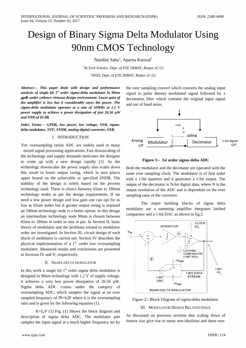
K=fn/F (1) Fig. (1) Shows the block diagram and
description of sigma delta ADC. The modulator part
samples the input signal at a much higher frequency set by
the over sampling convert which converts the analog input
signal to pulse density modulated signal followed by a
decimation filter which contains the original input signal
and out of band noise.
Figure 1:- 1st order sigma delta ADC
Both the modulator and the decimator are operated with the
same over sampling clock. The modulator is of first order
with a 1-bit quantize and it generates a 1-bit output. The
output of the decimator is N-bit digital data, where N is the
output resolution of the ADC and is dependent on the over
sampling ratio of the converter.
The major building blocks of sigma delta
modulator are a summing amplifier integrator latched
comparator and a 1-bit DAC as shown in fig.2.
Figure 2:- Block Diagram of sigma-delta modulator.
III. MODULATOR DESIGN RELATED ISSUE
As discussed on previous sections that scaling down of
feature size give rise to many non-idealities and these non-
T Modulator Decimator
Oversampling Clock Analog
I/P
1-bit PDM O/P
n-bit digital O/P

INTERNATIONAL JOURNAL OF SCIENTIFIC PROGRESS AND RESEARCH (IJSPR) ISSN: 2349-4689
Issue 93, Volume 33, Number 02, 2017
www.ijspr.com IJSPR | 115
idealities are due to MOS switches and capacitor involved
in the Op-Amp. Reducing the supply voltage in lower
technology nodes also give rise to unmanageable noise
effects and hence a degraded SNR results.
Nonlinear capacitance which are voltage dependent
capacitor contribute to overall nonlinearity of the
modulator because of this the voltage reference must
remain below permissible limit. The sampling at the
reference voltage used in the modulator can cause ringing
[2]. This mismatch is generally related to Op-Amp only.
But DAC used in the feedback path is also a critical block
in the design of modulators. DAC can introduce delay in
the feedback path which directly adds up to input of the
integrator. This results excess delay in the pulses at the
output which in turn can cause jitter and due to finite slew
rate of the op-amp this problem becomes more severe.
In order to keep the circuit simple and to reduce no of
devices, a binary modulator with class-A opamp is chosen
to design a high resolution and high linearity sigma delta
modulator.
IV. CIRCUIT DESIGN FOR 1ST
ORDER SIGMA DELTA
MODULATOR
A step by step approach is adopted here to design the
circuit of binary modulator. The design of circuit starts with
the design of Op-Amp Integrator and its performance
characterization. Further the design carries has been carried
out for comparator and the DAC.
A. Circuit and Block diagram of summing amplifier
The summing amplifier of the sigma delta modulator serves
as the summing point of the signal arriving from the 1-bit
DAC with the input signal.
Figure 3:- Summing amplifier Schematic diagram.
The summing amplifier consists of a differential pair MOS
transistor NM0-NM1 as an input to the output signal of
DAC and the actual input sinusoidal signal. The signal
from DAC is added to the input signal with help of this
differential pair.
B. Design of Op-Amp Integrator
The first block in the design process of binary sigma delta
modulator is integrator which acts as a low pass filter is
integrator. The transfer function of the integrator is,
𝐻(𝑠) =1
𝑆+1 (1)
Op-Amp drives the capacitive load to filter the out of band
noise. The Op-Amp schematic in cadence using gpdk90nm
is shown in fig. 3 and the block diagram of integrator
generated is shown in fig 4.
Figure 4:- Schematic diagram of Op-amp.
Circuit diagram shown in fig. 4 consists of conventional
class-A opamp. The input differential pair here integrates
the signal arriving from the summing amplifier. A
MOSCAP from the gpdk is chosen for area efficient layout,
also the capacitor here dynamic pole compensation to
increase the bandwidth. One more nMOS NM10 is added
to the output push-pull amplifier for gain enhancement.
Figure 5:- AC response of the opamp.
The AC response of the opamp shows that the gain of the
op-amp is 30.61dB. The phase margin of the opamp is 80
degrees and the unity gain frequency of is 1.28MHz. Input
bandwidth of the amplifier is 20 MHz which is sufficient
for the correct functioning of the modulator.

INTERNATIONAL JOURNAL OF SCIENTIFIC PROGRESS AND RESEARCH (IJSPR) ISSN: 2349-4689
Issue 93, Volume 33, Number 02, 2017
www.ijspr.com IJSPR | 116
Figure 6:- Transient response of the Op-amp.
The transient result of the opamp in fig. 6 shows that for
an input signal of 200mVPP the output is 300mVPP.
Figure 7:- Block diagram of the Integrator.
Block diagram of in fig. 7 shows the test bench of
integrator. The signal from the input and 1-bit DAC
summed at summing amplifier is processed by integrator.
The function of integrator here is to filter out sampling in-
band noise.
Figure 8:- Transient simulation result of integrator.
For the square wave input to the integrator gives a pulsed
output at half and fourth of the Vref. The simulation
performed for 100ns for the input signal of 1.25 VPP.
C. Comparator design
The role of comparator in sigma-delta converter is to
convert the analog input into the 1-bit digital output with
oversampling ratio of 250. The comparator used in this
design is discrete comparator because it has least
propagation delay.
Figure 9:-Schematic of the latch.
Comparator shown in fig. 9 consists of a preamplifier,
latch, self-biased circuit and an output driver. Transistor
Mn1 and Mn2 gates are driven by +Vref and the input
sinusoid, drain terminal of these two transistor are
connected to the inverter pair Mn4-Mn5 and Mp3-Mp4
which acts as dynamic latch i.e. two inverter connected
back to back. This type of latch is having advantage that it
dissipates less power since no current is flowing in the reset
mode. Transistor Mn4 and Mp7 acts as output driver which
pulls up the signal from latch to supply, Mp5, Mp2, Mp1
and Mp6 acts as clocking input.
Figure 10:- Simulation result of comparator.
The output of comparator trigger to 1.2 V when the input
signal greater than the reference voltage which is equal to
0.1 V while when the input signal lower than the reference
voltage, the comparator will trigger the output to 0V.
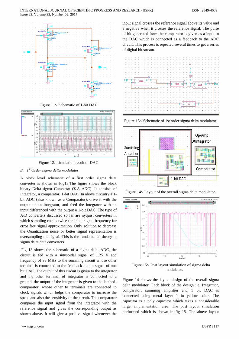
D. 1-Bit DAC
Conversion from form digital to analog signal here is
accomplished with the 1 bit digital to analog converter
which is comprises of two inverter connected back to back
i.e. one inverter output is fed to second inverter’s input.
The length of the MOS transistor is kept large in order to
introduce a comparable large delay because of the signal
excursion takes a large time and signal varies slowly
towards supply and back to ground thus signal can be
converted to analog signal again. Fig 11 & 12 shows the
schematic and simulation of DAC.
INTERNATIONAL JOURNAL OF SCIENTIFIC PROGRESS AND RESEARCH (IJSPR) ISSN: 2349-4689
Issue 93, Volume 33, Number 02, 2017
www.ijspr.com IJSPR | 117
Figure 11:- Schematic of 1-bit DAC
Figure 12:- simulation result of DAC
E. 1st Order sigma delta modulator
A block level schematic of a first order sigma delta
converter is shown in Fig13.The figure shows the block
binary Delta-sigma Converter (Σ-Δ ADC). It consists of
Integrator, a comparator, 1-bit DAC. In above circuitry a 1-
bit ADC (also known as a Comparator), drive it with the
output of an integrator, and feed the integrator with an
input differenced with the output a 1-bit DAC. The type of
A/D converters discussed so far are nyquist converters in
which sampling rate is twice the input signal frequency for
error free signal approximation. Only solution to decrease
the Quantization noise or better signal representation is
oversampling the signal. This is the fundamental theory in
sigma delta data converters.
Fig 13 shows the schematic of a sigma-delta ADC, the
circuit is fed with a sinusoidal signal of 1.25 V and
frequency of 35 MHz to the summing circuit whose other
terminal is connected to the feedback output signal of one
bit DAC. The output of this circuit is given to the integrator
and the other terminal of integrator is connected to a
ground. the output of the integrator is given to the latched-
comparator, whose other to terminals are connected to
clock signals which helps the comparator to increase the
speed and also the sensitivity of the circuit. The comparator
compares the input signal from the integrator with the
reference signal and gives the corresponding output as
shown above. It will give a positive signal whenever the
input signal crosses the reference signal above its value and
a negative when it crosses the reference signal. The pulse
of bit generated from the comparator is given as a input to
the DAC which is connected as a feedback to the ADC
circuit. This process is repeated several times to get a series
of digital bit stream.
Figure 13:- Schematic of 1st order sigma delta modulator.
Figure 14:- Layout of the overall sigma delta modulator.
Figure 15:- Post layout simulation of sigma delta
modulator.
Figure 14 shows the layout design of the overall sigma
delta modulator. Each block of the design i.e. Integrator,
comparator, summing amplifier and 1 bit DAC is
connected using metal layer 1 in yellow color. The
capacitor is a poly capacitor which takes a considerable
larger implementation area. The post layout simulation
performed which is shown in fig 15. The above layout
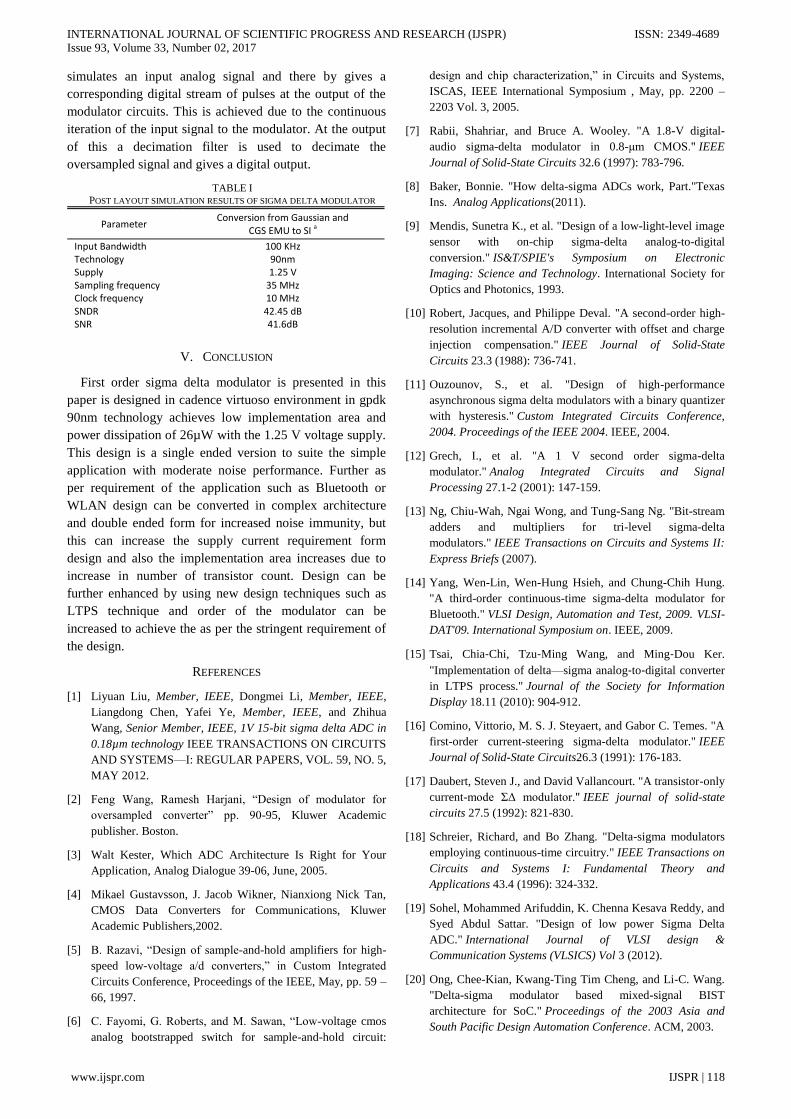
INTERNATIONAL JOURNAL OF SCIENTIFIC PROGRESS AND RESEARCH (IJSPR) ISSN: 2349-4689
Issue 93, Volume 33, Number 02, 2017
www.ijspr.com IJSPR | 118
simulates an input analog signal and there by gives a
corresponding digital stream of pulses at the output of the
modulator circuits. This is achieved due to the continuous
iteration of the input signal to the modulator. At the output
of this a decimation filter is used to decimate the
oversampled signal and gives a digital output.
V. CONCLUSION
First order sigma delta modulator is presented in this
paper is designed in cadence virtuoso environment in gpdk
90nm technology achieves low implementation area and
power dissipation of 26µW with the 1.25 V voltage supply.
This design is a single ended version to suite the simple
application with moderate noise performance. Further as
per requirement of the application such as Bluetooth or
WLAN design can be converted in complex architecture
and double ended form for increased noise immunity, but
this can increase the supply current requirement form
design and also the implementation area increases due to
increase in number of transistor count. Design can be
further enhanced by using new design techniques such as
LTPS technique and order of the modulator can be
increased to achieve the as per the stringent requirement of
the design.
REFERENCES
[1] Liyuan Liu, Member, IEEE, Dongmei Li, Member, IEEE,
Liangdong Chen, Yafei Ye, Member, IEEE, and Zhihua
Wang, Senior Member, IEEE, 1V 15-bit sigma delta ADC in
0.18µm technology IEEE TRANSACTIONS ON CIRCUITS
AND SYSTEMS—I: REGULAR PAPERS, VOL. 59, NO. 5,
MAY 2012.
[2] Feng Wang, Ramesh Harjani, ―Design of modulator for
oversampled converter‖ pp. 90-95, Kluwer Academic
publisher. Boston.
[3] Walt Kester, Which ADC Architecture Is Right for Your
Application, Analog Dialogue 39-06, June, 2005.
[4] Mikael Gustavsson, J. Jacob Wikner, Nianxiong Nick Tan,
CMOS Data Converters for Communications, Kluwer
Academic Publishers,2002.
[5] B. Razavi, ―Design of sample-and-hold amplifiers for high-
speed low-voltage a/d converters,‖ in Custom Integrated
Circuits Conference, Proceedings of the IEEE, May, pp. 59 –
66, 1997.
[6] C. Fayomi, G. Roberts, and M. Sawan, ―Low-voltage cmos
analog bootstrapped switch for sample-and-hold circuit:
design and chip characterization,‖ in Circuits and Systems,
ISCAS, IEEE International Symposium , May, pp. 2200 –
2203 Vol. 3, 2005.
[7] Rabii, Shahriar, and Bruce A. Wooley. "A 1.8-V digital-
audio sigma-delta modulator in 0.8-μm CMOS." IEEE
Journal of Solid-State Circuits 32.6 (1997): 783-796.
[8] Baker, Bonnie. "How delta-sigma ADCs work, Part."Texas
Ins. Analog Applications(2011).
[9] Mendis, Sunetra K., et al. "Design of a low-light-level image
sensor with on-chip sigma-delta analog-to-digital
conversion." IS&T/SPIE's Symposium on Electronic
Imaging: Science and Technology. International Society for
Optics and Photonics, 1993.
[10] Robert, Jacques, and Philippe Deval. "A second-order high-
resolution incremental A/D converter with offset and charge
injection compensation." IEEE Journal of Solid-State
Circuits 23.3 (1988): 736-741.
[11] Ouzounov, S., et al. "Design of high-performance
asynchronous sigma delta modulators with a binary quantizer
with hysteresis." Custom Integrated Circuits Conference,
2004. Proceedings of the IEEE 2004. IEEE, 2004.
[12] Grech, I., et al. "A 1 V second order sigma-delta
modulator." Analog Integrated Circuits and Signal
Processing 27.1-2 (2001): 147-159.
[13] Ng, Chiu-Wah, Ngai Wong, and Tung-Sang Ng. "Bit-stream
adders and multipliers for tri-level sigma-delta
modulators." IEEE Transactions on Circuits and Systems II:
Express Briefs (2007).
[14] Yang, Wen-Lin, Wen-Hung Hsieh, and Chung-Chih Hung.
"A third-order continuous-time sigma-delta modulator for
Bluetooth." VLSI Design, Automation and Test, 2009. VLSI-
DAT'09. International Symposium on. IEEE, 2009.
[15] Tsai, Chia‐Chi, Tzu‐Ming Wang, and Ming‐Dou Ker.
"Implementation of delta—sigma analog‐to‐digital converter
in LTPS process." Journal of the Society for Information
Display 18.11 (2010): 904-912.
[16] Comino, Vittorio, M. S. J. Steyaert, and Gabor C. Temes. "A
first-order current-steering sigma-delta modulator." IEEE
Journal of Solid-State Circuits26.3 (1991): 176-183.
[17] Daubert, Steven J., and David Vallancourt. "A transistor-only
current-mode ΣΔ modulator." IEEE journal of solid-state
circuits 27.5 (1992): 821-830.
[18] Schreier, Richard, and Bo Zhang. "Delta-sigma modulators
employing continuous-time circuitry." IEEE Transactions on
Circuits and Systems I: Fundamental Theory and
Applications 43.4 (1996): 324-332.
[19] Sohel, Mohammed Arifuddin, K. Chenna Kesava Reddy, and
Syed Abdul Sattar. "Design of low power Sigma Delta
ADC." International Journal of VLSI design &
Communication Systems (VLSICS) Vol 3 (2012).
[20] Ong, Chee-Kian, Kwang-Ting Tim Cheng, and Li-C. Wang.
"Delta-sigma modulator based mixed-signal BIST
architecture for SoC." Proceedings of the 2003 Asia and
South Pacific Design Automation Conference. ACM, 2003.
TABLE I
POST LAYOUT SIMULATION RESULTS OF SIGMA DELTA MODULATOR
Parameter Conversion from Gaussian and
CGS EMU to SI a
Input Bandwidth 100 KHz Technology 90nm
Supply 1.25 V Sampling frequency 35 MHz Clock frequency 10 MHz SNDR 42.45 dB SNR 41.6dB
INTERNATIONAL JOURNAL OF SCIENTIFIC PROGRESS AND RESEARCH (IJSPR) ISSN: 2349-4689
Issue 93, Volume 33, Number 02, 2017
www.ijspr.com IJSPR | 119
[21] Al-Alaoui, Mohamad Adnan, and Rony Ferzli. "An enhanced
first-order sigma-delta modulator with a controllable signal-
to-noise ratio." IEEE TRANSACTIONS ON CIRCUITS AND
SYSTEMS—I: REGULAR PAPERS53.3 (2006).
[22] Aziz, Pervez M., Henrik V. Sorensen, and J. Vn der Spiegel.
"An overview of sigma-delta converters." IEEE signal
processing magazine 13.1 (1996): 61-84.
[23] Li, Y., & He, L. (2007, March). First-Order Continuous-
Time Sigma-Delta Modulator. In ISQED (pp. 229-232).
[24] Van Engelen, J. A., Van De Plassche, R. J., Stikvoort, E., &
Venes, A. G. (1999). A sixth-order continuous-time bandpass
sigma-delta modulator for digital radio IF. IEEE Journal of
Solid-State Circuits, 34(12), 1753-1764.
[25] Wismar, U., Wisland, D., & Andreani, P. (2007, September).
A 0.2 V, 7.5 μW, 20 kHz ΣΔ modulator with 69 dB SNR in
90 nm CMOS. In Solid State Circuits Conference, 2007.
ESSCIRC 2007. 33rd European (pp. 206-209). IEEE.
[26] Muhammad, K., Ho, Y. C., Mayhugh, T. L., Hung, C. M.,
Jung, T., Elahi, I., ... & Vemulapalli, S. K. (2006). The first
fully integrated quad-band GSM/GPRS receiver in a 90-nm
digital CMOS process. IEEE Journal of Solid-State
Circuits, 41(8), 1772-1783.


![Reliability simulation in CMOS 90nm design using Eldoekv.epfl.ch/wp-content/uploads/2019/02/13_Chiittoor_MOS-AK.pdf · [6] Y.Leblebiciand S M Kang, “Hot-carrier reliability of MOS](https://static.fdocuments.in/doc/165x107/5d37d32588c993c93f8dfc5e/reliability-simulation-in-cmos-90nm-design-using-6-yleblebiciand-s-m-kang.jpg)