Design of a Wireless Firing Interface for a Power Electronic...
73
ECE 4600 Group Design Project Design of a Wireless Firing Interface for a Power Electronic Converter by Group 12 Brennan Martin Jason Gole Luchen Song Meng Wang Final report submitted in partial satisfaction of the requirements for the degree of Bachelor of Science in Electrical and Computer Engineering in the Faculty of Engineering of the University of Manitoba Academic Supervisor(s) Dr. Ani Gole, Dr. Cyrus Shafai Department of Electrical and Computer Engineering University of Manitoba Date of Submission March 10, 2014 Copyright © 2014 Brennan Martin, Jason Gole, Luchen Song, Meng Wang
Transcript of Design of a Wireless Firing Interface for a Power Electronic...

ECE 4600 Group Design Project
Design of a Wireless Firing Interface for a PowerElectronic Converter
byGroup 12
Brennan Martin Jason GoleLuchen Song Meng Wang
Final report submitted in partial satisfaction of the requirements for the degree of
Bachelor of Science in Electrical and Computer Engineering in the
Faculty of Engineering of the University of Manitoba
Academic Supervisor(s)
Dr. Ani Gole, Dr. Cyrus ShafaiDepartment of Electrical and Computer Engineering
University of Manitoba
Date of Submission
March 10, 2014
Copyright © 2014 Brennan Martin, Jason Gole, Luchen Song, Meng Wang


Wireless Power Converter
Abstract
Background: Power Electronic converters are devices that convert electricity from one
form to another, such as AC-DC, DC-AC or DC-DC. Typically, the turn on-off command, or
”firing pulses” are delivered using wired connections. In large converters, these connections
are a safety hazard as they allow a path for electricity to arc to ground. In this design
project, we detail the design, construction, and testing of a wireless firing mechanism for a
DC-DC power electronic converter. Our proposed approach will greatly simplify the design
of firing circuits in the future, as the power electronic components are completely physically
isolated from the controller.
Results: Following design and testing, we have successfully fired a DC-DC converter of
our own design completely wirelessly, with no connections to ground at any point in the
system. We demonstrate that the system can successfully drive a dynamic inductive load,
such as a DC-DC motor. We also demonstrate that feedback of voltage levels produced by
the converter is possible, and make provision for such.
Conclusion: We have successfully fired a DC-DC converter wirelessly. Although demon-
strated with the specific example of a DC-DC converter motor drive, the developed method
is easily extendable to any other class of square wave PWM converters, such as an inverter,
or a controlled rectifier.
- i -

Wireless Power Converter
Contributions
Bre
nn
anM
art
in
Jas
onG
ole
Lu
c hen
Son
g
Men
gW
an
g
GUI Design •Transmitter/Receiver Design • Driver Design • Converter Design •
Legend: • Lead task Contributed
- ii -

Wireless Power Converter
Acknowledgements
We would like to thank the following people for their assistance with this project:
• Dr. Ani Gole, for proposing this project, for taking the time to meet with us every
week, and for always having a helpful suggestion to give.
• Dr. Cyrus Shafai, for getting us the stuff we needed, even before we needed them,
and for all the help debugging our converter.
• Daniel Card, for his helpful advice, and his attention to the details that we missed.
• Sinisa Janjic, for getting us our parts, and for dealing with our unreasonable requests
in a reasonable manner.
• Erwin Driks, for answering so many of our questions, and not getting mad at us
constantly pestering him.
• Alan Mackay, for letting us eat in the project room.
• Tomas Vega, for helping us with our simulations.
• Jack Martin, for letting us steal all his tools.
• Dexter Williams, for being completely invaluable, and getting us this far in the project.
Without him, we would never have gotten this far. Sorry for calling you in so many
times.
• Dr. Ahmad Byagowi, for trying to get us replacement parts at 8:30 on a Saturday
night.
• Finally, our classmates, for (presumably) stealing all the chips off of our board and
costing us lots of money.
- iii -

Wireless Power Converter TABLE OF CONTENTS
Table of Contents
Abstract . . . . . . . . . . . . . . . . . . . . . . . . . . . . . . . . . . . . . . . . . i
Contributions . . . . . . . . . . . . . . . . . . . . . . . . . . . . . . . . . . . . . . ii
Acknowledgements . . . . . . . . . . . . . . . . . . . . . . . . . . . . . . . . . . . iii
List of Figures . . . . . . . . . . . . . . . . . . . . . . . . . . . . . . . . . . . . . vii
Nomenclature . . . . . . . . . . . . . . . . . . . . . . . . . . . . . . . . . . . . . . ix
1 Introduction 1
1.1 Motivation . . . . . . . . . . . . . . . . . . . . . . . . . . . . . . . . . . . . 1
1.2 Scope . . . . . . . . . . . . . . . . . . . . . . . . . . . . . . . . . . . . . . . 1
2 Overview 3
2.1 GUI . . . . . . . . . . . . . . . . . . . . . . . . . . . . . . . . . . . . . . . . 4
2.2 Microcontroller System . . . . . . . . . . . . . . . . . . . . . . . . . . . . . . 4
2.3 Driver Circuit . . . . . . . . . . . . . . . . . . . . . . . . . . . . . . . . . . . 4
2.4 DC-DC Converter . . . . . . . . . . . . . . . . . . . . . . . . . . . . . . . . 4
3 Methodology 6
3.1 GUI . . . . . . . . . . . . . . . . . . . . . . . . . . . . . . . . . . . . . . . . 6
3.1.1 Software Development Tools . . . . . . . . . . . . . . . . . . . . . . . 6
3.1.2 GUI Controls . . . . . . . . . . . . . . . . . . . . . . . . . . . . . . . 8
3.1.3 GUI Displays . . . . . . . . . . . . . . . . . . . . . . . . . . . . . . . 9
3.1.4 Serial Connection . . . . . . . . . . . . . . . . . . . . . . . . . . . . . 10
3.2 Wireless System . . . . . . . . . . . . . . . . . . . . . . . . . . . . . . . . . 15
3.2.1 Transmitter System . . . . . . . . . . . . . . . . . . . . . . . . . . . 15
3.2.2 Receiver System . . . . . . . . . . . . . . . . . . . . . . . . . . . . . 20
3.2.3 Transmitter Coding . . . . . . . . . . . . . . . . . . . . . . . . . . . 21
3.2.4 XBee Configuration . . . . . . . . . . . . . . . . . . . . . . . . . . . 24
- iv -

Wireless Power Converter TABLE OF CONTENTS
3.3 Driver Circuit . . . . . . . . . . . . . . . . . . . . . . . . . . . . . . . . . . . 26
3.3.1 Driver Requirements . . . . . . . . . . . . . . . . . . . . . . . . . . . 26
3.3.2 Bootstrap Theory . . . . . . . . . . . . . . . . . . . . . . . . . . . . 27
3.3.3 Bootstrap capacitor . . . . . . . . . . . . . . . . . . . . . . . . . . . 28
3.3.4 Bootstrap Diode . . . . . . . . . . . . . . . . . . . . . . . . . . . . . 30
3.3.5 Gate Resistor . . . . . . . . . . . . . . . . . . . . . . . . . . . . . . . 30
3.3.6 Final Considerations . . . . . . . . . . . . . . . . . . . . . . . . . . . 31
3.4 Converter Design . . . . . . . . . . . . . . . . . . . . . . . . . . . . . . . . . 32
3.4.1 Converter function . . . . . . . . . . . . . . . . . . . . . . . . . . . . 32
3.4.2 Components . . . . . . . . . . . . . . . . . . . . . . . . . . . . . . . 32
3.5 Converter Implementation . . . . . . . . . . . . . . . . . . . . . . . . . . . . 36
3.5.1 Safety . . . . . . . . . . . . . . . . . . . . . . . . . . . . . . . . . . . 36
4 Results and Observations 38
4.1 Unit Tests . . . . . . . . . . . . . . . . . . . . . . . . . . . . . . . . . . . . . 38
4.1.1 GUI Testing . . . . . . . . . . . . . . . . . . . . . . . . . . . . . . . . 38
4.1.2 Microcontroller Testing . . . . . . . . . . . . . . . . . . . . . . . . . 40
4.1.3 IGBT Driver Circuit Testing . . . . . . . . . . . . . . . . . . . . . . 41
4.1.4 Converter Test . . . . . . . . . . . . . . . . . . . . . . . . . . . . . . 42
4.1.5 PCB Testing . . . . . . . . . . . . . . . . . . . . . . . . . . . . . . . 43
4.2 System Test . . . . . . . . . . . . . . . . . . . . . . . . . . . . . . . . . . . . 45
5 Budget 47
6 Conclusions 52
7 Future Work 54
7.1 GUI . . . . . . . . . . . . . . . . . . . . . . . . . . . . . . . . . . . . . . . . 54
7.2 Microcontroller System . . . . . . . . . . . . . . . . . . . . . . . . . . . . . . 54
7.3 Driver Circuitry . . . . . . . . . . . . . . . . . . . . . . . . . . . . . . . . . . 55
7.4 Converter . . . . . . . . . . . . . . . . . . . . . . . . . . . . . . . . . . . . . 55
References 57
Appendix A A: Source Code and Other Files 58
Appendix B B: Circuit Diagrams 59
- v -

Wireless Power Converter TABLE OF CONTENTS
Appendix C C: Curriculum Vitae 63
- vi -

Wireless Power Converter LIST OF FIGURES
List of Figures
2.1 Basic Project Block Diagram . . . . . . . . . . . . . . . . . . . . . . . . . . 3
3.1 Graphical User Interface . . . . . . . . . . . . . . . . . . . . . . . . . . . . . 7
3.2 Help Window . . . . . . . . . . . . . . . . . . . . . . . . . . . . . . . . . . . 10
3.3 Transmission Flow Chart . . . . . . . . . . . . . . . . . . . . . . . . . . . . 13
3.4 Receiving Flow Chart . . . . . . . . . . . . . . . . . . . . . . . . . . . . . . 14
3.5 XBee Module and Pinout[1] . . . . . . . . . . . . . . . . . . . . . . . . . . . 16
3.6 PIC18F4xK22 Pinout [2] . . . . . . . . . . . . . . . . . . . . . . . . . . . . . 16
3.7 Parallax XBee 5V/3.3V Converter Board[3] . . . . . . . . . . . . . . . . . . 17
3.8 Sparkfun RS232 Converter Board[4] . . . . . . . . . . . . . . . . . . . . . . 17
3.9 DAC8562 Pinout[5] . . . . . . . . . . . . . . . . . . . . . . . . . . . . . . . . 18
3.10 Battery Fail Detect circuit[6] . . . . . . . . . . . . . . . . . . . . . . . . . . 19
3.11 Final Transmitter Topology . . . . . . . . . . . . . . . . . . . . . . . . . . . 20
3.12 Final Receiver Topology . . . . . . . . . . . . . . . . . . . . . . . . . . . . . 22
3.13 ISR Flowchart . . . . . . . . . . . . . . . . . . . . . . . . . . . . . . . . . . 23
3.14 Main Routine Flowchart . . . . . . . . . . . . . . . . . . . . . . . . . . . . . 25
3.15 IR2127 . . . . . . . . . . . . . . . . . . . . . . . . . . . . . . . . . . . . . . . 27
3.16 Bootstrap Circuit . . . . . . . . . . . . . . . . . . . . . . . . . . . . . . . . 28
3.17 Final Driver Design . . . . . . . . . . . . . . . . . . . . . . . . . . . . . . . 31
3.18 Converter Circuit Schematic . . . . . . . . . . . . . . . . . . . . . . . . . . . 33
3.19 Inductor . . . . . . . . . . . . . . . . . . . . . . . . . . . . . . . . . . . . . . 34
3.20 Finished Converter Circuit . . . . . . . . . . . . . . . . . . . . . . . . . . . . 37
4.1 Output of Wave Generator . . . . . . . . . . . . . . . . . . . . . . . . . . . 41
4.2 Output of IGBT Driver Circuit . . . . . . . . . . . . . . . . . . . . . . . . . 42
4.3 IGBT Driver Test Circuit . . . . . . . . . . . . . . . . . . . . . . . . . . . . 43
- vii -

Wireless Power Converter LIST OF FIGURES
4.4 Transmitter PCB . . . . . . . . . . . . . . . . . . . . . . . . . . . . . . . . . 44
5.1 First Parts Order . . . . . . . . . . . . . . . . . . . . . . . . . . . . . . . . . 48
5.2 Second Parts Order . . . . . . . . . . . . . . . . . . . . . . . . . . . . . . . . 49
5.3 Third Parts Order . . . . . . . . . . . . . . . . . . . . . . . . . . . . . . . . 50
5.4 Personal Expenditure and Total . . . . . . . . . . . . . . . . . . . . . . . . . 51
B.1 Transmitter Schematic . . . . . . . . . . . . . . . . . . . . . . . . . . . . . . 59
B.2 Transmitter PCB Design (Actual Size) . . . . . . . . . . . . . . . . . . . . . 60
B.3 Receiver Schematic . . . . . . . . . . . . . . . . . . . . . . . . . . . . . . . . 61
B.4 Receiver PCB Design . . . . . . . . . . . . . . . . . . . . . . . . . . . . . . . 62
- viii -

Wireless Power Converter LIST OF FIGURES
Nomenclature
Symbol Description
PWM Shorthand for Pulse Width Modulation.
ADC Analog to Digital Converter.
DAC Digital to Analog Converter.
UART Universal Asynchronous Receiver Transmitter.
RS232 12 V UART Connection.
IGBT Insulated Gate Bipolar Transistor.
GUI Graphical User Interface.
0x(letters) Denotes Hexadecimal Numbers.
DIO Digital IO.
IA Input Address.
Baud Signalling Events per Second.
PCB Printed Circuit Board.
PID Proportional Integral Derivative.
MCU Micro Controller Unit.
RSSI Received Signal Strength Indication.
RJ-11 Registered Jack 11.
EMF Electromotive Force.
COM Communication Port.
DPDT Double Pole Double Throw.
ISR Interrupt Service Routine.
- ix -

Wireless Power Converter 1. Introduction
Chapter 1
Introduction
1.1 Motivation
Power converters are electrical devices designed to convert electrical power from one form to
another, such as DC-DC, DC-AC or AC-DC. These converters operate by repeatedly firing
semiconductor switches in a set pattern in order to produce the desired electrical output.
Typically, these switches are fired using wired connections. However, large power converters
operate in the range of kV, and these wires present a potential path to ground, which is a
huge safety hazard. Whilst fibre optic connections provide one solution, these are expensive
and fragile. A wireless system would present no isolation problems, and would theoretically
be cheaper to implement. In this paper, we implement a complete wireless firing solution,
capable of firing a DC-DC converter of our own design.
1.2 Scope
Rather than attempting to design a wireless control system for an industrial sized converter,
we chose instead to design a system to control a smaller converter, designed for laboratory
applications. In order to limit the scope of the project, we chose to implement a firing
- 1 -

Wireless Power Converter 1.2 Scope
system for a DC-DC converter known as a chopper. This is the simplest form of DC-
DC converter, as it contains only one switching element. We chose to construct our own
converter, rather than purchase one. However, we intend to design the system to be capable
of firing other similar single element converters. In order to demonstrate the functionality
of our converter, we decided to drive a DC motor with our converter, rather than a static
inductive load. In order to provide information to the user, we decided to include some
sensing elements in our design. Specifically, we chose to include a voltage sensor to read the
output of the converter. We also chose to implement a simple matching routine, in order
to deal with non idealities in the converter. While not a proper control system, the routine
will emulate the effect of integral feedback, reducing the steady state error to zero.
- 2 -

Wireless Power Converter 2. Overview
Chapter 2
Overview
The goal of this project is to wirelessly control a DC-DC converter. In order to accomplish
this goal, we need to construct four main components. A GUI capable of controlling the
system, a microcontroller system capable of wirelessly gathering data and firing the con-
verter, a driver circuit capable of firing the switching element, and the DC-DC converter
itself 5.4.
Fig. 2.1: Basic Project Block Diagram
- 3 -

Wireless Power Converter 2.1 GUI
2.1 GUI
To create a user friendly GUI, the C# programming language was used in addition to the
Microsoft Visual Studio integrated development environment. To provide the user with
a meaningful interface, several controls were implemented, as well as displays to provide
feedback. The program used to design the GUI is also able to transmit data using a serial
connection.
2.2 Microcontroller System
In order to meet the wireless requirement of the system, we chose the 802.15.4 wireless
protocol, due to its relative simplicity, and low power consumption. To control the system
itself, and keep complexity to a minimum, we chose an 8 bit microcontroller from Microchip.
The microcontroller is coded in the C programming language, and communicates with both
the wireless system and the GUI via serial connections.
2.3 Driver Circuit
The wireless system is incapable of firing the converter directly, necessitating the inclusion
of a discrete driver circuit. The driver circuit operates on the principle of bootstrapping in
order to drive the converter, providing a differential voltage to the semiconductor switching
elements.
2.4 DC-DC Converter
The converter is based on a chopper topology, periodically interrupting a DC source voltage
to produce a lower voltage output. The switching element is an IGBT, which is capable of
handling both large currents and high switching frequencies. In order to provide constant
- 4 -

Wireless Power Converter 2.4 DC-DC Converter
current to the load, we include a large external inductor.
- 5 -

Wireless Power Converter 3. Methodology
Chapter 3
Methodology
3.1 GUI
The GUI provides an easy way for a user to control the system, using a variety of buttons,
numerical boxes and drop down boxes. Displays allow the user to see the condition of
elements within the system. Using serial communication, the GUI is then able to transmit
data based on the users inputs to the microcontroller within the system, and receive data
from the microcontroller concerning the condition of the system. The final design of the
GUI can be seen below 5.4.
3.1.1 Software Development Tools
Our GUI was created and tested on a PC running Microsofts Windows 7 operating system.
The code was developed and tested using Microsoft Visual Studio Express 2013, a free to
download integrated development environment (IDE). Visual Studio provides a user friendly
way to create GUIs. Visual Studio comes with templates to develop user interfaces using
Windows forms familiar to any Windows user. Built in toolboxes contain many controls
that allow the designer to add features such as buttons, text boxes, drop down selection
- 6 -

Wireless Power Converter 3.1 GUI
Fig. 3.1: Graphical User Interface
boxes and picture boxes to the GUI. The simplicity of the IDE and the ability to acquire a
free version from Microsoft were key factors in the decision to create our GUI using Visual
Studio.
Visual Studio allows the user to create Windows forms using the C# and Visual Basic
programming languages. C# is a flexible language, and many resources are available to help
in developing code, courtesy of the Microsoft Developer Network [7]. C# is also similar to
the C programming language. Several team members were familiar with the C programming
language, but our knowledge concerning Visual Basic was lacking. This familiarity with the
similar C language and the available support lead us to use C# to program the final GUI.
- 7 -

Wireless Power Converter 3.1 GUI
3.1.2 GUI Controls
The final design of the GUI incorporates several controls. The Port Selector drop down box
allows the user to select a desired port to connect the PC to the system when running the
program. If no COM ports exist on the given computer, nothing will be selectable, and the
program will not allow the user to try to start transmitting data. This user controllable
port selector provides increased flexibility for the user, as the user may use any given COM
port on their computer, as opposed to needing to connect to a predefined COM port. It is
therefore necessary that the user knows which port is to be used based on how they have
connected the PC and the system.
After selecting the COM port, the Start button becomes available to the user. The
Start button allows the user to decide when to start transmitting data. When the Start
button is selected by the user, an internal timer is activated. From this point on, the
program will transmit the user’s selected data every 300ms. The Stop button can then
be used to stop the transmission of data. When the Stop button is selected, the program
will transmit a stop command to the system, resetting all values to zero and closing the
connection to the system. Upon closing the connection, the Port Selector drop down box
becomes re-selectable. The user is then freely able to reconnect with the same port, or
select a new port from the drop-down box. This allows a user to have multiple systems
attached to a single PC and easily switch between the different systems.
The Output Voltage box allows the user to enter the data that will determine how
the end device behaves. The user can select any voltage level from 0V to 24V. The dial
increments and decrements the voltage in values of one, but the user is freely able to input
the desired voltage level rounded to one decimal place. Any values outside of the boundaries
will automatically be converted to the nearest boundary number.
There are two possible ways to close the program. The first way is to use the exit
button in the top right corner of the window, represented by an x. The transmission of
- 8 -

Wireless Power Converter 3.1 GUI
data must be stopped, by using the Stop button, before this button may be selected. In
the event that the exchanging of data has not yet stopped, the program will report to the
user that the port is still open and will prevent the system from closing. A second Close
button is also included. This Close button behaves similarly to using both the Stop and x
buttons combined. After asking the user for verification to close the program, it will send
a termination signal to the system, close the port and then close the window. This can
function as a panic button in case the end device is behaving abnormally.
A Help button has also been implemented. This button opens up a second window
with information on how to use each control, and provides more information on what kind
of data each display is reporting back to the user. The Help window can be seen below in
Fig.3.2.
3.1.3 GUI Displays
The Actual Output Voltage display box reports back to the user the output voltage of the
system. The output voltage is measured on the other end of the system, and is then
transmitted to the GUI. Two boxes are also used to indicate the current condition of
the batteries within the system. The Battery 1 indicator represents the battery on the
transmitter side of the system, and the Battery 2 indicator represents the battery on the
receiver side of the system. Both indicators are green when the batteries are in good
condition, but if the power in the battery drops below a certain threshold, the affected
battery indicator will change to red.
The Motor Speed display box would report back to the user the speed of the motor.
The hardware to gather this data was not implemented in the final design however.
- 9 -

Wireless Power Converter 3.1 GUI
Fig. 3.2: Help Window
3.1.4 Serial Connection
The PC connects to the system using an RS232 serial connection. When compared to other
connection types, such as USB, serial connections using RS-232 are easy to implement
using the C# programming language. Serial communication is well supported in the C#
programming language, whereas communication using USB protocols is not supported at
all, requiring user created libraries to function. A disadvantage with using RS-232 is that
many modern computers do not support it, and are thus missing the appropriate ports. To
accommodate for this, we used a USB to RS-232 adaptor. This adaptor allowed us to use
a USB port on a computer to create the serial connection, while still using the C# serial
communication functions in the program itself. PCs running Windows 7 will automatically
- 10 -

Wireless Power Converter 3.1 GUI
install the necessary drivers to use the adaptor, allowing this device to be used on most
modern day computers with little effort made by the user.
All code to develop the serial connection was made in the same program that created
the GUI. Based on the port selected by the user, the program will establish a connection
to the system. The baud rate is set to 4800 Baud within the program, and is not able to
be modified by the user.
After establishing the serial connection, there are two main aspects to the program;
sending and receiving data. The sending of data is accomplished in the main thread. A
flow chart representing this routine can be seen in Figure 3.3. After the user presses the
start button, a timer is started. At set time intervals, hardcoded within the program and
not modifiable by the user, a timer routine in the program will activate, which in turn calls
a transfer of data routine. Within this data transfer routine, the user data is formatted in
such a way that it can be read by the receiving microcontroller. This first byte indicates
the type of data that is being transmitted, while the second and third bytes contain the
actual data. After being formatted, the data is written to the serial port. A closely related
second transfer routine is also called when the user tries to close the connection between
the pc and the system, either by using the Stop or Close buttons.
- 11 -

Wireless Power Converter 3.1 GUI
The receiving of data from the system is more complicated. A flow chart of this routine
can be seen in Figure 3.4. When the user creates the connection to the system, a data
received event handler is created. This event handler functions similarly to an interrupt.
When the program senses that data has been received, a received data routine is called,
regardless of the condition of the rest of the program. This routine runs on a different
thread than the transfer routine, meaning that it will not slow down the transmission of
data. Within the receive data routine, the data is read into a byte array. The receive data
routine then invokes a routine in the main thread that processes the received data. The
data that is read is formatted in a similar way to the transmitted data, and must therefore
be decoded to find what the data represents. The first byte contains information regarding
what type of data it is, such as output voltage or battery strength. The second and third
bytes contain the actual data, such as the voltage level. The processing routine then converts
the data in the second and third bytes into the appropriate data. Once converted, the data
is then able to be displayed back to the user.
- 12 -

Wireless Power Converter 3.1 GUI
Fig. 3.3: Transmission Flow Chart
- 13 -

Wireless Power Converter 3.1 GUI
Fig. 3.4: Receiving Flow Chart
- 14 -

Wireless Power Converter 3.2 Wireless System
3.2 Wireless System
The wireless system has 3 primary tasks. First, it must be capable of both receiving from
and transmitting to the PC based GUI. Second, it has to be capable of either generating
or transmitting PWM signals to drive the converter. Third, it has to be capable of reading
the voltage output of the converter.
3.2.1 Transmitter System
As wireless communication is the central requirement of our system, we decided to select
a wireless module first, and then design the rest of the system around it. Ultimately, our
team settled on a pair of XBee series 1 modules 3.9. These modules communicate with
other devices using a standard UART, and offer a variety of useful features. Of particular
interest to us was the digital and analog line passing modes of the XBee radios. The
digital line passing mode allows us to drive a pin on the receiver module by driving the
same pin on the transmitter module. The analog line passing mode allows us to feed a
pin an analog reference voltage, and have the receiver output a 15.625 kHz PWM signal of
equivalent average voltage [8]. Originally, we decided to use the digital line passing mode
to pass individual firing pulses to the converter, allowing us to generate any type of PWM
wave we wanted. However, this proved unworkable, so we decided to utilize the analog
line passing mode to drive our converter. The XBee modules also offer analog to digital
conversion, allowing us to use them to read any sensors we chose to use without adding a
microcontroller on the converter side of the system.
Choosing the XBee modules allowed us to select the rest of the components in our
system. As the XBee modules use a UART, and we were also using a UART to connect to the
interface, we required a microcontroller with two UART ports. This proved to be a difficult
requirement to satisfy, as most of the available microcontrollers we looked at had only one
UART. We eventually settled on the PIC18F46K22 3.9, an 8 bit microcontroller available
- 15 -

Wireless Power Converter 3.2 Wireless System
Fig. 3.5: XBee Module and Pinout[1]
from Microchip. This device had two UART ports, and more than enough processing power
to service our system.
Fig. 3.6: PIC18F4xK22 Pinout [2]
Unfortunately, the choice of the PIC left us with a dilemma. The XBee radios are 3.3V
devices, and the PIC is a 5V device, meaning that we could not directly connect them. To
solve this problem, we decided to use a pair of Parallax 5V/3.3V XBee converter boards 3.9.
These boards provided 3.3V regulated power to the XBee, and also acted as bidirectional
logic level converters, allowing the devices to communicate via UART.
Another level conversion problem was encountered in connecting to the PC interface.
RS232 is a 12V signaling protocol, which is too much voltage for our microcontroller to
tolerate. To allow the PIC to communicate with the PC, we required another logic level
- 16 -

Wireless Power Converter 3.2 Wireless System
Fig. 3.7: Parallax XBee 5V/3.3V Converter Board[3]
Fig. 3.8: Sparkfun RS232 Converter Board[4]
converter. In order to save development time, we decided to buy instead of build such a
device. We chose a Sparkfun RS232-UART converter board 3.9 to meet this requirement.
- 17 -

Wireless Power Converter 3.2 Wireless System
The decision to use the XBee analog line passing mode to generate PWM required us
to include a DAC in the system. Whilst the PIC has a built in 5 bit DAC, we felt that
this device would be provide insufficient accuracy, as the ADC that the XBee uses for its
analog line passing mode is a 10 bit device. The combination of linearity and quantization
errors would be magnified by the reduced number of bits, and throw off our voltage level
significantly. Thus, we decided to use a discrete external DAC for this purpose. We chose
the DAC8562 3.9, a 12 bit parallel input DAC with a direct voltage output. Our lack of
other external devices allowed us to use a simple parallel interface, and its direct voltage
output spared us from having to include extra conversion circuitry. As the XBee is a 3.3V
device, its own ADC recognizes 3.3V as full scale for its analog line passing mode, whilst the
full scale of the DAC is 4.095V. Rather than correct the mismatch in software and sacrifice
some accuracy, we used a parallel resistor network to scale the DAC voltage down to 3.3V.
This allowed us maximum accuracy from the available devices.
Fig. 3.9: DAC8562 Pinout[5]
As an added feature, we decided to add a battery fail detector to both our transmitter
and receiver boards. We felt that this was important, as having insufficient battery power
- 18 -

Wireless Power Converter 3.2 Wireless System
to fire the converter on the receiver side would be disastrous. To implement this, we chose a
pair of MAX8211 chips, which are specifically designed to operate as battery fail detectors.
Selecting a trigger voltage for these chips was a simple matter of designing a 3 resistor
network 3.10 according to the following equations:
R2 = R1 ∗ (VU − 1.15)/1.15 (3.1)
R3 = R2 ∗ (VL − 1.15)/(VU − VL) (3.2)
Fig. 3.10: Battery Fail Detect circuit[6]
Where VL is the lower trip point, and VU is the upper trip point. For the transmitter
circuit, we set the upper trip point as 6.25V, limited by the need for the voltage regulator
to step the voltage down. For the receiver circuit, we set the upper trip voltage to 16.25V,
in order to provide sufficient voltage for the driver circuit.
Combining the various circuits described here, we arrived at the following final system
topology 3.11. In addition, several other components were added. An RJ-11 jack for
debugging the PIC, an on/off switch and power LED, and LED’s indicating power failures
on both the receiver and transmitter board. As well, we decided to put the entire circuit
- 19 -
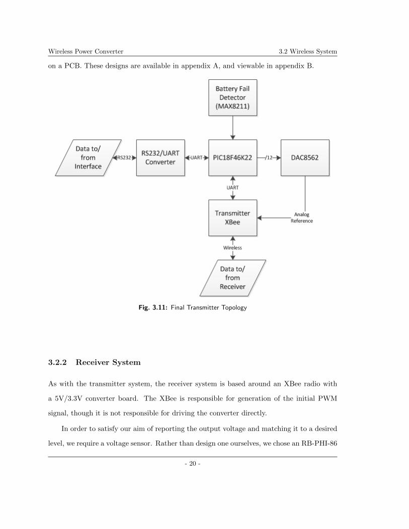
Wireless Power Converter 3.2 Wireless System
on a PCB. These designs are available in appendix A, and viewable in appendix B.
Fig. 3.11: Final Transmitter Topology
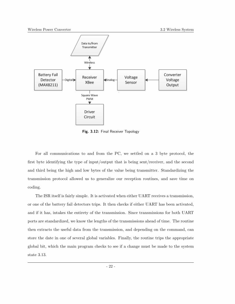
3.2.2 Receiver System
As with the transmitter system, the receiver system is based around an XBee radio with
a 5V/3.3V converter board. The XBee is responsible for generation of the initial PWM
signal, though it is not responsible for driving the converter directly.
In order to satisfy our aim of reporting the output voltage and matching it to a desired
level, we require a voltage sensor. Rather than design one ourselves, we chose an RB-PHI-86
- 20 -

Wireless Power Converter 3.2 Wireless System
voltage sensor[9]. This sensor runs on 5V, delivers a direct voltage output between 5V and
0V, and senses voltages in the range of +30V to -30V. This more than meets our needs, as
we only intend to drive a 24V motor. Again, we find that the sensor outputs voltages above
that that can be recognized by the XBee, so we need to scale down the maximum voltage
using a resistor divider. As well, we also decided to include a simple capacitive low pass
filter to improve the output. (picture of resistor divider here).
Putting the entire system together, we arrive at the following final system topology 3.12
In addition to the components listed above, we decided to include several other components.
A pair of pins, a DPDT switch, and a pair of pull down resistors to allow external access to
the XBee UART, as well as a power LED, and a second resistor divider in case we wanted
to add another RB-PHI sensor, or other 5V sensor. As with the transmitter board, we
decided to put the entire circuit on a PCB, alongside the IGBT driver. These designs are
available in appendix A, and viewable in appendix B.
3.2.3 Transmitter Coding
The transmitter microcontroller has several tasks to complete. It has to translate incoming
commands from the interface into voltage outputs for the XBee, accept inputs from the
receiving end XBee and translate them for the interface, and notify the interface when a
battery fail detector is tripped. All of these functions involve the UART ports, and it is
conceivable that whilst executing one function, the microprocessor could be interrupted by
another UART transmission, or an interrupt could cause the processor to miss a transmission
entirely. For this reason, we chose to break the code up into two parts: we did all of the
UART transmission/reception routines in interrupts, and did the rest of the program in
the main routine. This way, we can spend less time in the ISR, where we could miss a
transmission.
- 21 -
Wireless Power Converter 3.2 Wireless System
Fig. 3.12: Final Receiver Topology
For all communications to and from the PC, we settled on a 3 byte protocol, the
first byte identifying the type of input/output that is being sent/receiver, and the second
and third being the high and low bytes of the value being transmitter. Standardizing the
transmission protocol allowed us to generalize our reception routines, and save time on
coding.
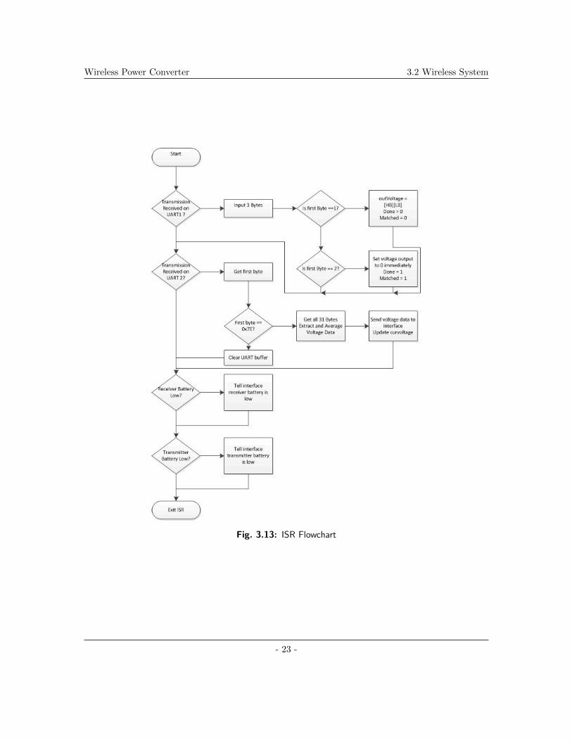
The ISR itself is fairly simple. It is activated when either UART receives a transmission,
or one of the battery fail detectors trips. It then checks if either UART has been activated,
and if it has, intakes the entirety of the transmission. Since transmissions for both UART
ports are standardized, we know the lengths of the transmissions ahead of time. The routine
then extracts the useful data from the transmission, and depending on the command, can
store the date in one of several global variables. Finally, the routine trips the appropriate
global bit, which the main program checks to see if a change must be made to the system
state 3.13.
- 22 -
Wireless Power Converter 3.2 Wireless System
Fig. 3.13: ISR Flowchart
- 23 -

Wireless Power Converter 3.2 Wireless System
The main routine handles the time intensive side of the processing. Specifically, it
handles the voltage ramping and matching functionality of the system. We must ramp
the duty cycle of the PWM wave available to the motor in order to avoid damage to the
converter caused by inrush current from the motor. This requires a great deal of time in
computing terms, on the order of ms. As well, due to the repetitive nature of the matching
operation, we chose to include this in the main routine instead of the ISR. We also decided
to include a routine to adjust the output voltage of the converter in response to the desired
output voltage. We chose to implement a simple successive approximation routine, rather
than a full control system. The matching routine emulates the effect of an integral feedback
control system reducing the steady state error to zero, though it has a much slower response
3.14.
3.2.4 XBee Configuration
The XBee modules must be properly configured to produce the desired PWM wave[8],
sample the voltage sensor, and to communicate with each other properly. In order for the
XBee radios to communicate with each other, we must give them each a unique address, and
give all of them the same PAN ID number. This is accomplished by programming the radios
using an adapter board, and a program called XCTU. We selected the transmitter radio as
0x01, and the remote radio as 0x02, and chose the PAN ID as 0x3332. We then select the
baud rate for both radios as 4800. This is half of the standard 9600 that the radios usually
operate at, but in testing we discovered that 9600 baud transmissions between processor
and XBee were unreliable. Cutting the baud rate significantly improved the reliability of
the system. In order to setup the PWM module, we set DIO 1 to ADC mode, and set a
sampling rate of 1ms, the fastest that the radios are capable of. On the receiving radio, we
enable PWM module 1, and then set the IA parameter of the receiving radio to 0xFFFF,
allowing the transmitting radio access to the receiving radios pins. To setup reading of the
- 24 -

Wireless Power Converter 3.2 Wireless System
Fig. 3.14: Main Routine Flowchart
- 25 -

Wireless Power Converter 3.3 Driver Circuit
voltage sensor, we set the (i forget which pin it is) to ADC mode, set a sampling period of
200ms, and set the radio to buffer 5 samples. This is so we can average several values over
time, in order to minimize the effect of any ripple in the output voltage. For the battery fail
detector, we set (i forget which pin) on the receiving radio to digital input, and set (same
pin) on the transmitter radio to digital output. We also set the IA parameter to 0xFFFF
to allow the receiving radio access to the transmitter’s pins.
3.3 Driver Circuit
Our wireless system is incapable of firing the IGBT in the DC-DC converter by itself.
Therefore, we require a driver circuit to interpose between them. In the driver circuit, the
gate pin of the IGBT will be fed a PWM wave. The PWM wave will the IGBT on and
off. This circuit is intended to operate in a high power environment, thus we cannot use
standard ICs, and must use specialized active and passive components instead.
3.3.1 Driver Requirements
To be able to properly drive the IGBT, the gate voltage must be higher than the emitter
voltage. The IGBT used in this project requires a nominal 15V difference between the Gate
and Emitter voltage to operate[?]. On the other hand, the IGBT driver circuit will receive
a logic output from the XBee on the receiver side. This logic input is a 3.3V PWM wave
and has a frequency of 15.625kHz [8]. Therefore, to drive the IGBT properly, the IGBT
driver circuit needs to amplify the 3.3V PWM wave to an 18V PWM wave. Because IC
chips will not be used on the receiver side, an optical coupler will not be required in this
circuit. To meet these requirements, we selected the IR2127 3.15. This specialized IC is
intended to drive both IGBTs and MOSFETs in power converters.
The IR2127 is the core component of the IGBT driver circuit. It is capable of taking
a logic input high at a minimum value of 3V, which is lower than the XBee logic output
- 26 -

Wireless Power Converter 3.3 Driver Circuit
Fig. 3.15: IR2127
voltage 3.3V. Reading from the datesheet of the IR2127 [10], the output voltage is in the
range of Vs to Vb. Vs is the high side floating offset voltage, which has a range of -5V
to 600V. Vb is the high side floating supply voltage, which is in the range of Vs+12V to
Vs+20V. Since, these are all floating voltages; Vs can be connected to the ground to set
the offset voltage to zero voltages. Then, the output of IR2127 will range from 0V to 20V,
which is capable of turning on the IGBT. As the receiver end circuit will be power by a
pair of 9V batteries, the power supply will be 18V. The supply voltage for IR2127 is in the
range of -0.3V to 25V. This means that the power supply can supply enough power to the
driver to fire IGBT.
3.3.2 Bootstrap Theory
The operation of IR2127 chip is basically a bootstrap circuit as seen in figure3.16. When
the IGBT is fired, the IGBT needs to be pushed into saturation state. To saturate the
IGBT, we need to deliver a differential voltage across its gate and emitter pins. Building a
bootstrap circuit is a simple and inexpensive way to accomplish this. There is a bootstrap
- 27 -

Wireless Power Converter 3.3 Driver Circuit
Fig. 3.16: Bootstrap Circuit
capacitor in the above figure 3.16. When Vs connects to ground, the bootstrap capacitor
will be charged from the 18V supply, causing the Vbs to reach 18V [11]. When charged, the
capacitor is connected across the IGBT, turning it on. In order to make sure this circuit
operates properly, the value of bootstrap diode, bootstrap capacitor and gate resistor must
be chosen properly.
3.3.3 Bootstrap capacitor
If the value of bootstrap capacitor is not correctly calculated, Vbs will have a large amount
of ripple. Vbs will fall below the IGBT turn on voltage [11]. Based on the application notes
of the IR2127 [12], the bootstrap capacitor will be discharged when the IGBT is on, and
the capacitor will be charged when the IGBT is off. Thus, the basic formula for calculating
the value of the bootstrap capacitor is:
- 28 -

Wireless Power Converter 3.3 Driver Circuit
Cboot =QTOTAL
∆VBOOT(3.3)
∆VBOOT is the capacitor drop voltage, which is depends on the voltage between the
gate and the emitter.
∆VBOOT = VDD − VF − VGEMIN (3.4)
In this project, VDDis the receiver supply voltage, which is 18V. VF = 1V. VGEMIN =
12V. As a result,∆VBOOT = 5V.
QTOTAL is the total amount of the charge supplied by the capacitor, which needs to
satisfy the following equation:
QTOTAL = QGATE + (ILKCAP + ILKGS + IQBS + ILK + ILKDIODE) + tON +QLS (3.5)
Where : QGATE = Total gate charge.(QGATE = 38nC) ILKGS= Switch gate-emitter
leakage current. (ILKGS = 10nA, this value does not specific for switch properties, in
this projector, this value is assumed to suit for switching properties) ILKCAP = Bootstrap
capacitor leakage current. (ILKCAP = 0A, since, the ceramic capacitor is used here) IQBS=
bootstrap circuit quiescent current. (IQBS = 200µA) ILK = bootstrap circuit leakage
current. ( ILK = 50µA) ILKDIODE = Bootstrap diode leakage current. ( ILKDIODE =
20µA) QLS = Charge required by the internal level shifter, which is set to 3nC for all HV
gate drivers. (QLS = 3 nC) tON = High-side switch on time.(For duty cycle = 50% at fs
= 15kHz.)
Then, tON = 33 µs. Finally, the value of Cboot is calculated to be about 10nF.
However, the value calculated by the above equations is the typical value. When the
bootstrap circuit is operating, the capacitor may work at its maximum value. However, if
- 29 -

Wireless Power Converter 3.3 Driver Circuit
we use 10nF, the capacitor may become overcharged and cause problems. Thus, in order to
make sure the bootstrap circuit operates properly, the value of bootstrap capacitor should
multiplied by a factor of 15 [11].Thus, the value of Cboot will be 150nF. Due to component
availability, we select Cboot as 200nF instead.
3.3.4 Bootstrap Diode
The bootstrap diode is intended to block the flow of charge from the bootstrap capacitor to
the voltage supply. When the IGBT is turned on, the bootstrap capacitor will be discharged.
This charge needs to be blocked from flowing back to the voltage supply. The IGBT driver
operates at a frequency of about 15kHz. This means that we require a fast recovery diode
to prevent charge leakage. Based on the application notes of IR2127, the maximum value
of trr is 100 ns[11]. We selected the UF4003, a fast recovery diode which has a trr of 50 ns
[13].
3.3.5 Gate Resistor
The gate resistor is another critical component in the bootstrapping circuit. The Gate
resistor can control the turn on and turn off current of the gate port of the IGBT. Thus, the
proper selection of gate resistor can optimize the switching speed and reduce the switching
loss of the IGBT. Based on the application notes of the IR2127 [12], the gate resistor is
divided into turn on resistor and turn off resistor. However, in this project, only the turn
on gate resistor is considered. The formula for calculating the gate resistor is:
RTotal =VDD − VGS(th))
Cgd(off) ∗ dVOUTdt
(3.6)
Where: VDD is the supply voltage for the IR2127. (VDD = 18 V) VGS(th)) is the Gate
threshold voltage. (VGS(th)) = 4.5 V) Cgd(off) is the miller effect capacitor, specified as
Crss. (Cgd(off) = 22 pF) dVOUTdt is the output slope of IR2127. ( dVOUT
dt = 50 Vns)
- 30 -

Wireless Power Converter 3.3 Driver Circuit
Based on the above equation, the value of RTotal 13 Ω. In practice, the value of RT otal
= 22 Ω.
3.3.6 Final Considerations
The IR2127 includes a current sensing feature. While useful, our system is intended to
be used with a variety of different converters. Thus, we have decided not to use this
functionality. To disable the current sensor, we connect the current sensing pin to ground,
and the sensor output to Vcc.
Combining all of the components, we arrive at the following final design:3.17
Fig. 3.17: Final Driver Design
- 31 -
Wireless Power Converter 3.4 Converter Design
3.4 Converter Design
3.4.1 Converter function
The purpose of the converter design is to demonstrate the capability of wireless firing in-
terface. The converter is a DC-DC converter, and the load is a DC motor. The purpose
of the converter circuit is to change the motor speed by changing the duty cycle from the
user interface. Furthermore, we want to keep the motor speed constant at our switching
frequency. We use an IGBT in the circuit as the semiconductor switch. The IGBT on/off
state is controlled from the user interface with wireless communication. The motor acceler-
ates when the IGBT in the converter circuit is on, and decelerates when it is off. Therefore,
the speed of the DC motor can be controlled from user interface.
The DC-DC converter circuit we implement in this project is called a chopper circuit.
It steps down the source voltage to a desired level to supply power to the load connected to
the circuit. When the IGBT is turned on, the dc source will keep charging the circuit. And
when the IGBT is off, the inductor in the circuit will continuously provide current to the
motor, and the free wheeling diode in the converter circuit can provide the back path for
the current to flow through. The current drops as the inductor discharges, and the current
will increase while the circuit is charged. The periodic charge and discharge creates current
ripples. The current ripples would cause the motor speed to fluctuate. Since the current
ripple can be controlled by the inductance, we add an inductor in the circuit to achieve the
desired current ripple level. The schematic of converter circuit is shown in figure 3.18.
3.4.2 Components
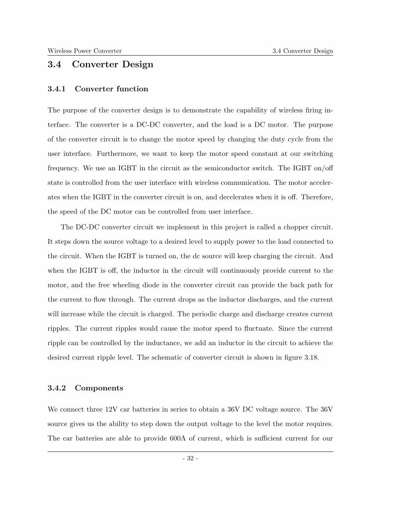
We connect three 12V car batteries in series to obtain a 36V DC voltage source. The 36V
source gives us the ability to step down the output voltage to the level the motor requires.
The car batteries are able to provide 600A of current, which is sufficient current for our
- 32 -
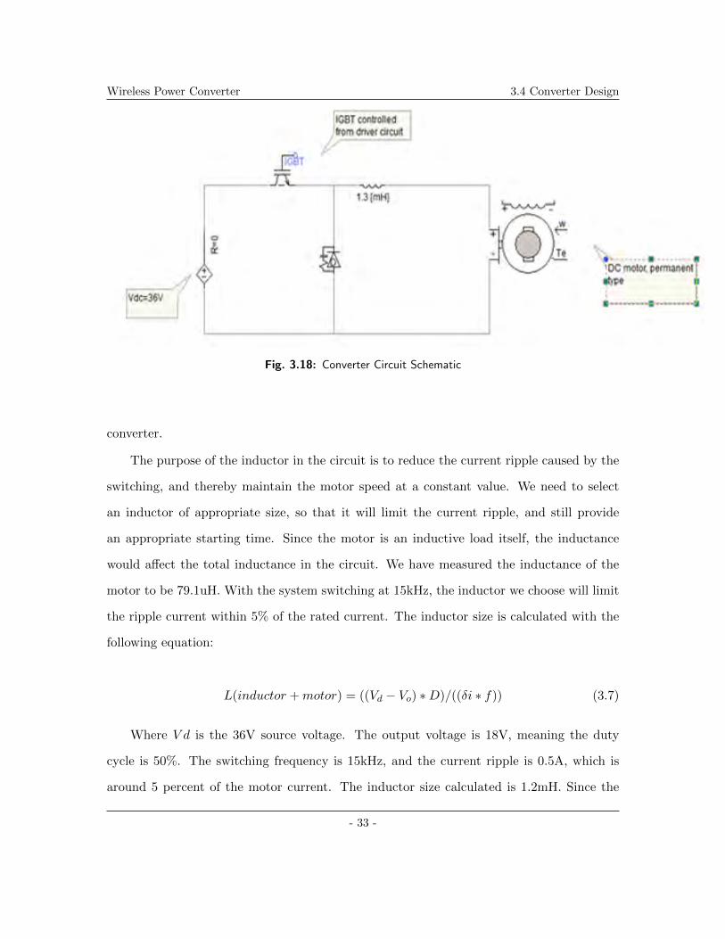
Wireless Power Converter 3.4 Converter Design
Fig. 3.18: Converter Circuit Schematic
converter.
The purpose of the inductor in the circuit is to reduce the current ripple caused by the
switching, and thereby maintain the motor speed at a constant value. We need to select
an inductor of appropriate size, so that it will limit the current ripple, and still provide
an appropriate starting time. Since the motor is an inductive load itself, the inductance
would affect the total inductance in the circuit. We have measured the inductance of the
motor to be 79.1uH. With the system switching at 15kHz, the inductor we choose will limit
the ripple current within 5% of the rated current. The inductor size is calculated with the
following equation:
L(inductor +motor) = ((Vd − Vo) ∗D)/((δi ∗ f)) (3.7)
Where V d is the 36V source voltage. The output voltage is 18V, meaning the duty
cycle is 50%. The switching frequency is 15kHz, and the current ripple is 0.5A, which is
around 5 percent of the motor current. The inductor size calculated is 1.2mH. Since the
- 33 -

Wireless Power Converter 3.4 Converter Design
motor has 79.1uH of inductance, the inductor size would be about 1.12mH. As the charging
duty cycle is changed from the user interface, the inductor size required to maintain the
current ripple level need to be varied as well. We choose an inductor that has three paths
3.19, so that we can adjust the inductance as required. The inductor is 1.3mH per path
and can be rated up to 3.9mH. The inductor current is rated 16A to 50A, which is suitable
for our design.
Fig. 3.19: Inductor
We control the on and off state of the IGBT semi-conductor switch to control the
charging time of the DC-DC converter circuit. The IGBT is turned on when the driver
circuit provides it with a gate-emitter voltage of 15V. We selected an IGBT to be the semi-
conductor switch, as it is suitable for our fast switching system, and has a relatively low
switching energy. The IGBT is rated 35A at 25C and 19A at 100C. Since the IGBT heats
up due to switching losses, the temperature increases significantly. Therefore, 19A is the
maximum current we allow in our system.
The turn-on time is 30ns and turn-off time is 230ns. Since our switching frequency is
- 34 -

Wireless Power Converter 3.4 Converter Design
15kHz, the period is 1/(15 kHz) = 66.7us. Therefore, the IGBT will have enough time to
turn on and off without the risk of commutation failure.
We are using 15kHz, which is a relatively high switching frequency. The IGBT expe-
riences more energy loss at high frequencies. Therefore, we chose an IGBT which has a
low switching loss rating to limit the energy loss and make the system more efficient. This
IGBT has switching losses of 390uJ when Ic is 10A and Vge is 15V. The IGBT module we
chose has a reverse direction diode built in to provide protection to the IGBT in case of a
reverse current situation.
The DC motor we implement as the load is a permanent magnet motor. It is rated at
24V, and the maximum voltage it can handle is 36V. Since the car batteries connected in
series provide no more than 36V to the output, the voltage source is safe for the motor,
even in case of a fault.
The resistance of the motor is very low. The back EMF is proportional to the armature
angular speed. And the back EMF is zero if the rotor of the motor is not rotating. So
the motor starting current would be very high without external control. The high starting
current may cause permanent damage to the motor and other circuit components. One
way to solve the problem is to add an adjustable resistor to limit the starting current and
manually change its resistance after the motor is fully started. However, this operation is
not desired for our design since we require wireless control of the converter. To limit the
starting current of the motor, we will limit the rate at which the duty cycle can be increased.
V = Ia ∗R+ Ea (3.8)
Ea = Ka ∗ φa ∗ w (3.9)
Where V is the source voltage, R is the motor resistance; Ea is the back EMF, Ka is
- 35 -

Wireless Power Converter 3.5 Converter Implementation
machine constant, φ is the magnetic flux, and w is the armature angular speed.
The free wheeling diode in the converter circuit provides a path for the current when
the IGBT is turned off. It is rated at 20A which is sufficient for the current in our circuit.
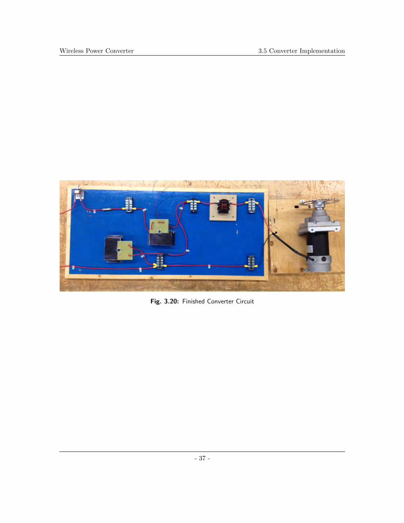
3.5 Converter Implementation
3.5.1 Safety
We implement the converter circuit on a wood board to provide insulation between the
converter circuit and ground. We added a fuse rated 20A at the high side of the circuit to
provide extra protection in the event of a fault. We also implemented a toggle switch to
turn the circuit on and off.
The cable terminals are clamped on ring connectors and connected with terminal blocks.
The cables are soldered to the IGBT and diode. Since the pins of the chips are very thin,
the torque that the soldered cables exert on the pins can break the pins easily. We mounted
the cables through pin boards to fix the cable position and reduce damage to the pins.
Breadboard jumper wires are soldered to the pins as well to connect to the driver circuit.
We use heat-shrink tube to cover the soldered connection between the pins and cables to
provide insulation, since the pins each chip are close to each other. The layout of the
converter is shown in figure 3.20.
- 36 -
Wireless Power Converter 3.5 Converter Implementation
Fig. 3.20: Finished Converter Circuit
- 37 -

Wireless Power Converter 4. Results and Observations
Chapter 4
Results and Observations
4.1 Unit Tests
Before assembling the entire system, we conducted a series of unit tests with the various
project components isolated from each other. This was done in order to discover and fix
as many problems as possible before assembling the project, rather than leaving all the
problems to be discovered at once.
4.1.1 GUI Testing
Before creating the GUI, we began developing several test programs to perform simple tasks.
These programs were created to operate individually, and therefore they did not interact
with any external programs or hardware. These test programs allowed us to become familiar
with creating user controls, such as buttons and text boxes. We also tested controlling
displays based on user input, such as updating a text box to reflect a button press made by
the user. Once we had the the controls working properly, an early design for the GUI was
created. This GUI was unable to connect to the system, but was able to respond to user
demands.
- 38 -

Wireless Power Converter 4.1 Unit Tests
After developing this early GUI, we started developing code that would allow us to
communicate with the system using the USB to RS-232 adaptor cable. The first step was
to create a program that could recognize the COM port, and create a connection with it.
We hardcoded the necessary data, such as the desired COM port and baud rate, into the
program and began testing. Using the provided data, the program was successfully able to
recognize the COM port and create a connection. The GUI was updated to make use of
this new feature. The next step was to allow the user to choose which COM port to use
to connect to the system. This feature was implemented using a drop down box. With the
user selectable COM port functioning, we were able to add the ability to prevent the user
from using certain controls without the COM port being selected.
With the connection established, the ability to write and read data needed to be im-
plemented. To test these features, more stand alone programs were developed. To test
writing data, we connected the computer running the program to an XBee, which in turn
was connected to another computer. The program would send data in the form of a packet
to the XBee, and we could see the data on the second computer connected to the XBee.
The data was being received by the XBee correctly and at predetermined intervals.
Reading data proved more difficult than writing. To test the reading routines, the
microcontroller was connected to an XBee. A specific set of bytes were transmitted to the
user side of the system, where it would be read and displayed. A problem occurred where
the data was not being read at the correct rate, resulting in incorrect values. To solve this
issue, we included a delay in the reading routine to allow the complete set of data to come
in before reading it. This concession slowed the transfer of data, but allowed us to receive
the data correctly. A second problem also occurred when it became known that because
the reading was conducted in a second thread apart from the main thread, it could not
directly update the displays on the GUI. To resolve this issue, we created a delegate in
the main thread that could be invoked by the reading thread, allowing the data from the
- 39 -

Wireless Power Converter 4.1 Unit Tests
reading thread to be transferred to the main thread and update the displays on the GUI.
After receiving generic data, we implemented the reading of voltages. A known voltage was
sent to the GUI, where it was then converted into displayable data. The data was being
displayed properly.
4.1.2 Microcontroller Testing
In order to test the microcontroller by itself, we need to generate inputs identical to those
generated by the GUI. To do this, we connected our XBee radio to the serial port used to
connect to the interface. We then used Digi’s XCTU software to generate packets identical
to those put out by the interface. We began by testing duty cycle ramping by, inputting
commands to the microcontroller. We repeatedly tested ramping the duty cycle up and
down. During testing, two bugs arose. Setting the duty cycle to zero froze the system, and
setting the duty cycle to 100% caused the duty cycle to go to zero. Both of these bugs were
traced to errors in the duty cycle ramping routine, and after a revision, both bugs were
fixed, with the added benefit of the system being able to handle desired voltages greater
than the source voltage. However, during testing, problems arose with the serial connection.
The connection was unreliable, and often failed completely. This problem was solved by
cutting the baud rate to 4800, and rewiring the system. We then began testing the battery
fail coding. By pulling the external interrupt pins high and low and observing the serial
output, we verified the functionality of the battery fail code. This code worked as intended,
and no changes were required. We then tested reading of voltage levels from the remote
sensor. After configuring the XBee radios, we connected the sensor to an adjustable DC
voltage. By adjusting the voltage and viewing the values received by the microcontroller
using breakpoints, we managed to verify the operation of the remote voltage sensor.
- 40 -

Wireless Power Converter 4.1 Unit Tests
4.1.3 IGBT Driver Circuit Testing
During the initial testing, a wave generator supplied a 3.3v PWM wave to the input of the
driver circuit to simulate the output of the XBee. An oscilloscope was used to detect the
output of the IGBT driver circuit. The test results are shown in the following figures 4.2,
4.1.
Fig. 4.1: Output of Wave Generator
After that, we neede to test the ability of the circuit to fire the IGBT. To test this, we
connected a yellow LED and a resistor in place of the converter. The circuit is shown in
figure 4.3.
We found that the LED would blink when the frequency of the PWM wave was below
50Hz. However, the operating frequency of the PWM in this project is 15.625kHz. When
the frequency of the output wave from the wave generator changes to 15.625kHz, human
- 41 -

Wireless Power Converter 4.1 Unit Tests
Fig. 4.2: Output of IGBT Driver Circuit
eyes can not perceive the blinking of the LED. But, the oscilloscope can detect the PWM
wave at the emitter of the IGBT. This test proved that the IGBT driver circuit was able
to turn on and turn off the IGBT, and it was ready to connect to the converter.
4.1.4 Converter Test
We tried to test the circuit with the car batteries, but without wireless control. After
supplying the voltage source to the converter circuit, the motor started without the IGBT
turned on. We found that the IGBT was very hot and the high temperature had damaged
the IGBT. We mounted a new IGBT and diode on a heat sink to prevent heat damage. We
then tried another test, however the same situation occurred. We believed that there could
be energy stored in the gate of the IGBT that caused the turn on of IGBT. We connected
- 42 -

Wireless Power Converter 4.1 Unit Tests
test final.png
Fig. 4.3: IGBT Driver Test Circuit
the gate to the ground to eliminate any charge left on the gate. However, it did not solve
the problem.
We then measured the connections to identify the shorting point that caused the failure.
We found that the IGBT collector is shorted to the anode of the diode, which is connected
to the emitter. This caused the collector to short to the emitter, which turned on the motor.
We cut the heat sink into two pieces and mounted the IGBT and diode on each piece. The
converter circuit then began to function properly.
4.1.5 PCB Testing
Before assembling the entire system, the PCB’s needed to be assembled and tested. The
transmitter PCB was half completed, with sockets soldered in for the microcontroller, DAC
and battery fail IC. We then attempted to debug the microcontroller using the RJ-11 jack
included on the board. This was unsuccessful, and subsequent inspection of the design
revealed a flaw in the RJ-11 connection design. To rectify this flaw, the RJ-11 connector
was removed from the board, and wires were soldered to the pins of the jack. These
wires were then inserted into the correct holes, and resoldered. However, this failed to
- 43 -

Wireless Power Converter 4.1 Unit Tests
fix the problem. As the RJ-11 jack was used only for debugging, and was not strictly
necessary to operate the system correctly, no further attempts to solve the problem were
made. Following the attachment of the other components 4.4, the system was tested with
the GUI. Reference voltage levels were correctly generated by the DAC in response to serial
inputs. The receiving end XBee correctly put out a PWM wave of appropriate duty cycle,
confirming the functionality of the PCB.
Fig. 4.4: Transmitter PCB
After uncovering the flaw in the transmitter PCB, the receiver PCB design was rechecked.
A flaw was discovered, with a pair of pins on the driver circuit incorrectly connected. This
offending trace was cut with a knife, and a wire was soldered into place to connect the pins in
the correct configuration. After chip sockets were soldered into the board, along with most
of the passive components, we attempted to test the driver circuit. Several unsuccessful
- 44 -

Wireless Power Converter 4.2 System Test
tests were conducted, and the circuit was implemented on a solder board instead.
4.2 System Test
The completed system was then assembled. As the modifications to the PCBs were not
complete at the time of the first test, the circuits were constructed on breadboards. The
GUI was first connected to the microcontroller via the RS232 adaptor. The interface was
then used to send desired voltage levels to the microcontroller, and the voltage output of
the DAC was monitored. The output voltage levels matched the desired values, and the test
was completed. The battery fail detection functionality of the interface was then tested,
using the same procedure detailed before. The GUI correctly indicated that both battery
fail detectors had tripped.
The output waveform of the receiving end XBee was then recorded, and was observed
to match the desired duty cycle, based upon the desired output voltage 4.1. The XBee
was then connected to the input of the driver circuit. The output of the driver circuit was
read using an oscilloscope 4.2. The driver circuit was then connected to the converter’s
IBGT. In order to limit the current drawn by the motor, and prevent damage to the system
by any unaccounted for transients, the system was run on 12V, rather than the desired
36V. The system worked as intended, and the motor began to turn. We attempted to
take waveforms of the output of the converter, but were unable to due to the lack of an
oscilloscope capable of handling the high current. A video of this test is available on the
CD attached to appendix A.
A second test was then conducted with the converter running at 24V. The noise pro-
duced by the inductor was markedly increased. Unexpectedly, the serial connection to the
microcontroller repeatedly cut out when the converter reached 25% maximum output. Re-
peated computer resets failed to solve the problem, and out of an abundance of caution,
an improvised Faraday cage was constructed from aluminium foil, and placed over the in-
- 45 -

Wireless Power Converter 4.2 System Test
ductor. The serial problems soon ended, and the noise produced by the inductor was much
reduced.
Following the construction of the transmitter PCB, the converter system was tested
again, and functioned identically to the previous test. We then attempted to test the
matching routine and voltage feedback. However, one of our XBee radios failed before we
could start the test. With no way to obtain replacement parts in a timely manner, testing
was halted.
- 46 -

Wireless Power Converter 5. Budget
Chapter 5
Budget
Over the course of the project, we ordered 3 primary rounds of components, with the first
round being worth about as much as the second and third combined. However, over the
course of the year, we found it necessary to order components on our own. We ordered on
our own, either due to the fact that we could not wait for the tech shop to send out a bulk
order, or because the tech shop was unavailable at the time. These components include a
pair of extra XBee radios that were used as replacements, after one of our original ones was
destroyed by careless wiring when the tech shop was closed. We also had to order several
replacement driver chips and IGBTs after a series of destructive tests. These purchases are
detailed in their own section in the budget report. Ultimately, we spent a grand total of
about $310 on components. We also had circuit boards made for both the transmitter and
receiver. In total, these cost $240, leaving us over our initial budget of $400, and well over
our initial $250 budget for the entire project. These expenditures are detailed below.
- 47 -

Wireless Power Converter
Fig. 5.1: First Parts Order
- 48 -

Wireless Power Converter
Fig. 5.2: Second Parts Order
- 49 -

Wireless Power Converter
Fig. 5.3: Third Parts Order
- 50 -

Wireless Power Converter
Fig. 5.4: Personal Expenditure and Total
- 51 -

Wireless Power Converter 6. Conclusions
Chapter 6
Conclusions
In large power converters, the wires delivering firing pulses to the switching elements present
a safety hazard, as they provide a path to ground. Firing the system wirelessly means that
we require no connections to ground anywhere in the system, removing any risk of arcing
along the control wires. We have demonstrated in this paper that it is in fact possible to
fire a simple DC-DC converter completely wirelessly.
To accomplish the task of firing a DC converter wirelessly, we created a PC based
GUI, a complete wireless microcontroller system, a DC converter, and driver circuitry to
fire it. Through use of the GUI, a user is able to select a desired output voltage. The
microcontroller system then translates this voltage level into a square wave PWM signal
on the receiving end of the system. This PWM signal is then fed into the driver circuitry,
which drives the converter.
Despite encountering several issues regarding differential grounding between the driver
and the converter, wireless firing issues, and a multitude of component failures, we ul-
timately achieved our primary objective. The system is capable of firing the converter
wirelessly, in response of user inputs. In the future, we wish to include the capability to
display output voltage levels to the user, and to match the output voltage level of the
- 52 -

Wireless Power Converter
converter based on these values. We had originally planned to include these features, and
they are present in current software, but a last minute component failure prevented us from
verifying their functionality.
- 53 -

Wireless Power Converter 7. Future Work
Chapter 7
Future Work
7.1 GUI
Selectable Source Voltage: While we had originally intended to have a selectable source
voltage, time constraints prevented us from fully implementing it. Adding in a selectable
source voltage would require changes to both the GUI and microcontroller system, but
would significantly improve the functionality of the system.
RSSI Indication: In the current system, the user has no way of knowing the received
signal strength from the microcontroller system. The ability to see the signal strength would
be an improvement in usability and safety.
Microcontroller Reset: In the event of a problem with the microcontroller, the only
recourse the user has is to power cycle the microcontroller board manually. The ability to
reset the microcontroller using the interface would solve this problem.
7.2 Microcontroller System
Sinusoidal PWM: Currently, the microcontroller system is capable of generating square
wave PWM at a single frequency. Adding the ability to generate other types of PWM, such
- 54 -

Wireless Power Converter 7.3 Driver Circuitry
a sinusoidal PWM would increase the number of different converters the system could be
used with. This addition would likely require either the addition of a microcontroller on
the receiving end, or a change of wireless module.
PID Control System: Currently, the microcontroller runs a simple matching routine
to achieve the desired output voltage. Whilst this does eventually reach the desired output
level, it is slow, and would be of limited utility in a system driving a loaded motor. Im-
plementing a proper PID or other control system would be a huge step up in functionality,
and would not require additional hardware.
Additional Sensor Outputs: Currently, the system only reports the output voltage
to the user. Ideally, such a system would report both this value, the source voltage, as well
as source and output current. This functionality would need to be implemented jointly with
the GUI, and would require the provisioning of new PCBs and new sensors.
7.3 Driver Circuitry
Desaturation Circuit: The desaturation circuit was designed and tested individually,
but did not make it into the eventual final product. Adding this circuit would improve the
safety of the system, but would require redesigning the PCBs.
Driver Starter Circuit: The current driver circuit is incapable of driving a converter
where an output voltage is present before firing, such as in a battery charger. Including a
driver start circuit would allow the circuit to fire the converter in such a situation.
7.4 Converter
Filtering Capacitor: Currently, the converter contains only inductive elements. Whist
this stabilizes the current, there are no elements present to stabilize the voltage output. In-
cluding a large capacitor at the output would change the converter into a full buck converter,
- 55 -

Wireless Power Converter 7.4 Converter
and deliver superior performance.
Inverter Conversion: The converter we have constructed is the simplest large scale
power converter topology. However, using the current interface and microcontroller system,
we could instead construct an inverter, or even an H-bridge converter. Whilst this would
require refactoring the driver circuitry, and require a new motor, it would be a massive step
up in usability.
- 56 -

Wireless Power Converter REFERENCES
References
[1] H. A. Kadir, “XBee,” http://urrg.eng.usm.my/index.php?option=com content&view=article&id=281:xbee-&catid=31:articles&Itemid=70, accessed: 2014-03-09.
[2] PIC18(L)F2X/4XK22 Data Sheet, Microchip, last Revised 2010.
[3] XBee 5V/3.3V Adapter, Parallax Inc, last Revised 2010.
[4] “RS232 Shifter SMD,” https://www.sparkfun.com/products/449, Sparkfun, Accessed:2014-03-09.
[5] DAC8562, Rev.A ed., Analog Devices, 2010.
[6] Microprocessor Voltage Monitors with Programmable Voltage Detection, Rev.5 ed.,Maxim Integrated, 2008.
[7] “MSDN Library,” http://msdn.microsoft.com/library, Microsoft, Accessed: 2014-03-09.
[8] XBee/XBee-PRO RF Modules, Digi International, March 2013.
[9] Product Manual 1135 - Precision Voltage Sensor, Rev.0 ed., Phidgets, 2009.
[10] Current Sensing Single Chnanel Driver, International Rectifier, Sep 2004.
[11] Design Tip Bootstrap Component Selection for Control IC’s, International Rectifier,Sep 2001.
[12] Design and Application Guide of Bootstrap Circuit for High-Voltage GAte-Drive IC,Fairchild semiconductor, Sep 2008.
[13] UF4001-UF4007 Fast Rectifiers, Fairchild Semiconductor, 2005.
- 57 -

Wireless Power Converter A. A: Source Code and Other Files
Appendix A
Source Code
Source code for both interface and microcontroller is located on the attached CD. Alsoincluded is PSCAD simulation files, EAGLE schematics, and EAGLE PCB designs.
- 58 -

Wireless Power Converter B. B: Circuit Diagrams
Appendix B
Circuit Diagrams
Below are the EAGLE schematic files for both the transmitter and receiver boards, as wellas PCB designs for both circuits.
Fig. B.1: Transmitter Schematic
- 59 -

Wireless Power Converter
Fig. B.2: Transmitter PCB Design (Actual Size)
- 60 -

Wireless Power Converter
Fig. B.3: Receiver Schematic
- 61 -

Wireless Power Converter
Fig. B.4: Receiver PCB Design
- 62 -