Design of a Two Stage Low Noise System in the Frequency...
6
Design of a Two Stage Low Noise System in the Frequency Band 1.8-2.2GHz Zhao Xiaorong 1,a , Fan Honghui 1,b , Ye Feiyue 1,c , Qian Xiufang 1,d , Chen Dan 1,e , He Sheng 1,f 1 College of Computer Engineering, Jiangsu University of Technology a [email protected], b [email protected], c [email protected], d [email protected], e [email protected], f [email protected] Abstract. In first stage of each microwave receiver there is Low Noise Amplifier (LNA) circuit, and this stage has important rule in quality factor of the receiver. This paper presents the design of LNA and development of low bias (VD=3V, ID=20mA), the LNA operating in frequency range 1.8-2.2GHz using a feedback circuit. Design System (ADS) 2012 tool was used for design and simulation, and each design was tuned to get the optimum value for NF, power gain (S21), input return loss (S11) and reverse isolation (S12). Simulation results have indicated that the S21 achieves 33.2515±0.4475dB over the wide frequency band of 1.8-2.2GHz, the gain was almost flat over the whole band. Noise Figure (NF) maintains is 0.4945 ± 0.0565dB, S12 < -47.089dB and S11 < -16.126 dB in the entire band. Key words: Low noise amplifier, HEMT, Feedback, Noise Figure, ADS 1 Introduction In the era of wireless communications, devices that are able to exchange information through modulated radio frequency waves acquire more and more importance. Wireless communication and its applications have travelled through rapid growth in recent years. Cellular systems, WLANS, Bluetooth as well as WPANs have undergone numerous generations of evolution in the swift development in wireless communication [1]. Although LNAs are parts of the receivers only, their design should take into account the general features of the whole communications system [2]. One of the key design goals for the LNA is a low noise contribution to the input signal, together with a good impedance matching to the signal source, a sufficiently large output signal dynamic range and a low power consumption. Most of the single stage LNA device in the review could only around 20 dB gain. It was proposed that the low noise amplifier should have a gain of at least 30 dB. So the proposed LNA will be designed by Two Stage. Advanced Science and Technology Letters Vol.75 (SIP 2014), pp.70-75 http://dx.doi.org/10.14257/astl.2014.75.17 ISSN: 2287-1233 ASTL Copyright © 2014 SERSC
Transcript of Design of a Two Stage Low Noise System in the Frequency...

Design of a Two Stage Low Noise System in the
Frequency Band 1.8-2.2GHz
Zhao Xiaorong1,a
, Fan Honghui1,b
, Ye Feiyue1,c
, Qian Xiufang1,d
,
Chen Dan1,e
, He Sheng1,f
1College of Computer Engineering, Jiangsu University of Technology
a [email protected], b [email protected],c [email protected], d [email protected], e
[email protected], f [email protected]
Abstract. In first stage of each microwave receiver there is Low Noise
Amplifier (LNA) circuit, and this stage has important rule in quality factor of
the receiver. This paper presents the design of LNA and development of low
bias (VD=3V, ID=20mA), the LNA operating in frequency range 1.8-2.2GHz
using a feedback circuit. Design System (ADS) 2012 tool was used for design
and simulation, and each design was tuned to get the optimum value for NF,
power gain (S21), input return loss (S11) and reverse isolation (S12).
Simulation results have indicated that the S21 achieves 33.2515±0.4475dB
over the wide frequency band of 1.8-2.2GHz, the gain was almost flat over the
whole band. Noise Figure (NF) maintains is 0.4945±0.0565dB, S12 <
-47.089dB and S11 < -16.126 dB in the entire band.
Key words: Low noise amplifier, HEMT, Feedback, Noise Figure, ADS
1 Introduction
In the era of wireless communications, devices that are able to exchange information
through modulated radio frequency waves acquire more and more importance.
Wireless communication and its applications have travelled through rapid growth in
recent years. Cellular systems, WLANS, Bluetooth as well as WPANs have
undergone numerous generations of evolution in the swift development in wireless
communication [1].
Although LNAs are parts of the receivers only, their design should take into
account the general features of the whole communications system [2]. One of the key
design goals for the LNA is a low noise contribution to the input signal, together with
a good impedance matching to the signal source, a sufficiently large output signal
dynamic range and a low power consumption.
Most of the single stage LNA device in the review could only around 20 dB gain. It
was proposed that the low noise amplifier should have a gain of at least 30 dB. So
the proposed LNA will be designed by Two Stage.
Advanced Science and Technology Letters Vol.75 (SIP 2014), pp.70-75
http://dx.doi.org/10.14257/astl.2014.75.17
ISSN: 2287-1233 ASTL Copyright © 2014 SERSC

2 LNA design
The designs of LNAs, there are several common goals. These contain minimizing the
NF of the amplifiers, providing gain with sufficient linearity, and supporting stable
input impedance are all-important considerations [3].
In order to make an LNA, the choice of transistor is critical. This is one of the most
important steps in designing a low-noise-amplifier (LNA). Different types of
transistors are available for LNA applications. According to specifications,
appropriate transistor should be selected for low-noise-amplifier due to its low NF and
high gain [4]. The numbers of transistors are limited at the interested frequency. In
this work, ATF54143 is chosen.
2.1 Bias Circuit Design
The S-parameters of the transistor are fixed and do not change as the correct bias
current is maintained. In order to meet the design goals for NF, intercept point and
gain, the drain source current(ID) was chosen to be 40mA. FET in the amplifier is
biased at a Vds of 3V and Id of 20mA, giving a total current of 40mA. As indicated
by the characterization data shown in the device data sheet, 20mA gives the best NF.
Also shown in the data sheet, a 3V drain to source voltage(Vds) gives a slightly higher
gain and is also preferred since it easily allows the use of a 5 V regulated supply.
2.2 Stability Analysis
The schematic diagram of simulating stability factor is shown in the Figure 1, Here,
the DC source of 5V supplies DC bias. C1, C2 are bypass capacitors, respectively.
where C1=C2=C3=C4=270pF. Actual models of capacitor in the above circuit were
adopted from the Murata Components Library for Agilent ADS. The accuracy and
efficiency of simulations have been improved, since physical effects of the layout
components were taken into account. C1 and C2 can improve the stability of low
frequency. In order to get unconditionally stable circuit, we can add negative feedback
inductor to the source of the transistor.
Advanced Science and Technology Letters Vol.75 (SIP 2014)
Copyright © 2014 SERSC 71
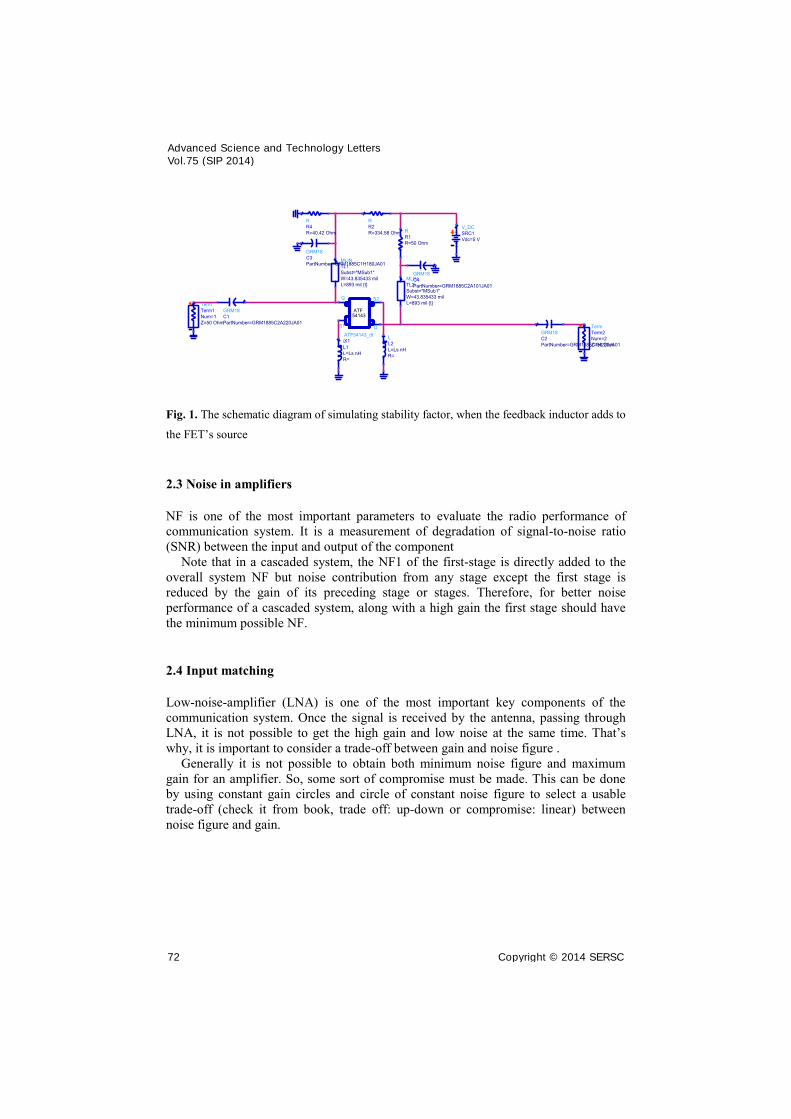
Fig. 1. The schematic diagram of simulating stability factor, when the feedback inductor adds to
the FET’s source
2.3 Noise in amplifiers
NF is one of the most important parameters to evaluate the radio performance of
communication system. It is a measurement of degradation of signal-to-noise ratio
(SNR) between the input and output of the component
Note that in a cascaded system, the NF1 of the first-stage is directly added to the
overall system NF but noise contribution from any stage except the first stage is
reduced by the gain of its preceding stage or stages. Therefore, for better noise
performance of a cascaded system, along with a high gain the first stage should have
the minimum possible NF.
2.4 Input matching
Low-noise-amplifier (LNA) is one of the most important key components of the
communication system. Once the signal is received by the antenna, passing through
LNA, it is not possible to get the high gain and low noise at the same time. That’s
why, it is important to consider a trade-off between gain and noise figure .
Generally it is not possible to obtain both minimum noise figure and maximum
gain for an amplifier. So, some sort of compromise must be made. This can be done
by using constant gain circles and circle of constant noise figure to select a usable
trade-off (check it from book, trade off: up-down or compromise: linear) between
noise figure and gain.
Advanced Science and Technology Letters Vol.75 (SIP 2014)
72 Copyright © 2014 SERSC

2.5 Analytical and circuit simulation results
The schematic of the proposed LNA is shown in Fig.7, the feedback inductor is
replaced by Microstrip lines, because the inductor is too small which is difficultly
designed. The input, interstage and output matching networks are composed of
microstrip lines. The LNA is composed of two stages. The designed circuit of Fig.2 is
simulated with ADS 2012 tools. TL1, TL2, TL4, TL5 and TL6 sizes art set to
L1=405.035433mil, L2=359.019291mil, L4=334.064493715mil, L5=115mil and
L6=26mil.
Fig. 2. Two Stage LNA schematic diagram
Fig. 3. Simulation result of S12
Advanced Science and Technology Letters Vol.75 (SIP 2014)
Copyright © 2014 SERSC 73

Fig. 4. Simulation result of S11
Fig. 5. Simulation result of the stability factor
Fig. 6. Simulation result of S21
Advanced Science and Technology Letters Vol.75 (SIP 2014)
74 Copyright © 2014 SERSC

The simulation results are shown in Fig.3, Fig.4, Fig.5, Fig.6. In Fig.3, S12 is less
than -47.089dB. In Fig.4, we can know S11 is below -16.126 dB in the entire band.
3 Conclusion
The proposed Two Stage LNA is good candidate for wireless applications due to its
low NF and high gain. Furthermore, throughout the whole design, transistor was
stable. The level of satisfaction of this thesis work is satisfactory. Though the
responses are satisfactory, but still there are scopes to improve the performances.
Some of the circuits can be improved in design and with more proper optimization to
have better responses. This thesis work gives a closer and wide view of all the
relevant background theories and design technologies to the designer.
References
1. G.Sharmila, E.G.Govindan. A Novel Design of Low-Noise RF Amplifier for Orthogonal
Frequency Division Multiplexing. Bonfring International Journal of Research in
Communication Engineering. 1,special(2011).
2. Anastasios Tsaraklimanis, Evangelia Karagianni. Low Noise Amplifier Design for Digital
Television Applications. Journal of Electromagnetic Analysis and Applications. 3,7(2011).
3. Zhen-hua LI, Bang-hong GUO, Zheng-jun WEI, Song-hao LIU, Nan CHENG. A
gain-flatness optimization solution for feedback technology of wideband low noise
amplifiers. Journal of Zhejiang University-SCIENCE C (Computer & Electronics).
12,7(2011).
4. Venkat Ramana. Aitha, Mohammad Kawsar Imam. Low Noise Amplifier for Radio
Telescope at 1.42 GHz. Computer and Electrical Engineering, Halmstad University, Sweden,
IDE0747, May 2007 pp. 29
5. Reinhold Ludwig,Gene Bogdanov. RF Circuit Design Theory and Applications Second
Edition. Publishing house of electronics industry,BeiJing. 2010.
Advanced Science and Technology Letters Vol.75 (SIP 2014)
Copyright © 2014 SERSC 75