Design of a Microwave Imaging System for Breast Cancer...
13
GROUP 5 ECE 4600 ECE 4600 FORMAL WRITTEN PROGRESS REPORT Design of a Microwave Imaging System for Breast Cancer Detection GROUP 5 GROUP MEMBERS Rebecca Gole Cameron MacGregor Kyle Nemez Michael Partyka Bo Woods DEPARTMENT SUPERVISOR Dr. Joe LoVetri CO-SUPERVISORS Dr. Puyan Mojabi Dr. Majid Ostadrahimi Covering the period of: May 1, 2013 to January 13, 2014 Submitted on: January 13, 2014
Transcript of Design of a Microwave Imaging System for Breast Cancer...
GROUP 5 ECE 4600
ECE 4600
FORMAL WRITTEN PROGRESS REPORT
Design of a Microwave Imaging System for Breast Cancer Detection
GROUP 5
GROUP MEMBERS
Rebecca Gole
Cameron MacGregor
Kyle Nemez
Michael Partyka
Bo Woods
DEPARTMENT SUPERVISOR
Dr. Joe LoVetri
CO-SUPERVISORS
Dr. Puyan Mojabi
Dr. Majid Ostadrahimi
Covering the period of: May 1, 2013 to January 13, 2014
Submitted on: January 13, 2014
GROUP 5 ECE 4600
FORMAL WRITTEN PROGRESS REPORT ii
Table of Contents
List of Acronyms………………………………………………..……... iii
1. Introduction………………………………………………………... 1
2. Progress……………………………………………………………. 1
2.1. Antennas…………………………………………………………………... 1
2.2. Frequency Synthesizer…………………………………………………….. 2
2.3. Probe Driver Circuit……………………………………………………….. 2
2.4. Homodyne Receiver……………………………………………………….. 2
2.5. Lock-In Amplifier…………………………………………………………. 3
2.6. Data Acquisition System and Controller………………………………….. 4
2.7. Phantom…………………………………………………………………… 4
3. Future Work………………………………………………………... 5
3.1. Antennas…………………………………………………………………... 5
3.2. Lock-In Amplifier…………………………………………………………. 5
3.3. Data Acquisition System and Controller………………………………….. 5
3.4. Phantom…………………………………………………………………… 5
4. Conclusion……………………………….………………………… 5
Appendix A – Gantt Chart….…………………………………………. 6
Appendix B – Budget..………………………………………………… 8
GROUP 5 ECE 4600
FORMAL WRITTEN PROGRESS REPORT iii
List of Acronyms
ADC – Analog-to-Digital Converter
CPLD – Complex Programmable Logic Device
DAQC – Data Acquisition System and Controller
EIL – Electromagnetic Imaging Laboratory
GPIB – General Purpose Interface Bus
LIA – Lock-In Amplifier
LO – Local Oscillator
LPF – Low Pass Filter
MWI – Microwave Imaging
PCB – Printed Circuit Board
RF – Radio Frequency
Rx – Receive or Receiver
Tx – Transmit or Transmitter
VSWR – Voltage Standing Wave Ratio
GROUP 5 ECE 4600
FORMAL WRITTEN PROGRESS REPORT PAGE 1 OF 10
1.0 Introduction
The aim of our project is to design and prototype the hardware required for a
novel microwave imaging (MWI) system intended for breast cancer detection. We are
also designing breast phantoms to test our system. Our project includes the design of all
hardware components except for the radio frequency (RF) switch and the low frequency
synthesizer. The functional system will consist of an antenna chamber into which the
phantom will be placed and subsequently illuminated by microwaves, a frequency
synthesizer that generates the microwaves, and a probe driver circuit (PDC) that
controls which waveguide slots act as transmitter (Tx) and receiver (Rx). In addition,
the system includes a homodyne receiver and a lock-in amplifier (LIA); both of which
serve to condition the signal measured at the receiving antenna. Lastly, a data
acquisition system and controller (DAQC) is included that is responsible for sampling
the conditioned signal and controls the scan.
2.0 Progress
Some components of the project are behind schedule, while other parts are ahead
of schedule (refer to Gantt chart, appendix A). Overall, progress has either met or
exceeded expectations in all aspects of the project.
2.1 Antennas
At the heart of the MWI system is the imaging chamber, containing 24 antennas,
which receive and transmit the signals required to generate an image. Each antenna,
designed to operate in water, consists of a waveguide with five selectable /2 slot
antennas on one face. At the onset of the project, Dr. Majid Ostadrahimi completed a
preliminary antenna design that required testing and refinement. Kyle refined the design
by adjusting the waveguide feed length, measuring the H-field distribution along the
waveguide, and measuring switching diode sensitivity. To prevent short-circuiting and
thus ensure adequate operation while submerged, a sprayable rubber compound was
found that could coat the exposed circuitry. Kyle was then responsible for designing the
printed circuit board (PCB) containing the slots once the dimensions and slot positions
were finalized. Manufacturing of the waveguide-based imaging chamber was contracted
out to the Cancer Care machine shop in Winnipeg. The PCBs have been manufactured,
GROUP 5 ECE 4600
FORMAL WRITTEN PROGRESS REPORT PAGE 2 OF 10
assembled, coated in the rubber compound, and sent to the Cancer Care machine shop for
final placement in the chamber. The antenna chamber assembly is almost complete. We
expect to receive the completed chamber from Cancer Care within three weeks.
2.2 Frequency Synthesizer
The frequency synthesizer generates the RF energy that is radiated by the transmit
antennas and drives the local oscillator (LO) port of the homodyne receiver. Since
commercial frequency synthesizer circuits are available at a lower cost than a new design,
an evaluation board from Analog Devices (ADF4351) was selected. The board was
designed by the manufacturer to be controlled by a computer, and Kyle successfully
modified the board to be controlled by the DAQC. Under initial testing, the 2nd
and 3rd
order harmonics were undesirably large, so a band pass filter was added. Kyle also chose
a power splitter and amplifier to split the filter output and deliver power to both the LO
port of the homodyne receiver and the Tx antenna. Testing and implementation of the
frequency synthesizer is complete.
2.3 Probe Driver Circuit
The probe driver circuit (PDC) allows the DAQC to control which slot transmits
and which slot receives microwaves. Kyle designed a logic circuit to control all 120 slots
with 16 digital control lines. To implement the design, two options were considered: a
number of discrete logic gates and a programmable logic device. A complex
programmable logic device (CPLD) based design was chosen because of its flexibility
and reliability.
To properly control the antenna slots, the logic level signals from the CPLD must
be translated to higher voltage switching signals. Kyle investigated several technologies
that could accomplish this translation. Darlington transistor pairs (ULN2803) were
selected because of their low cost, previous successful use in the lab, and sufficient
performance under our tests. Kyle subsequently designed two PCBs, one to mount the
CPLD and one to mount the translation circuitry. The finalized PCB designs were sent
for manufacturing and assembled upon reception. Work on the PDC is complete.
2.4 Homodyne Receiver
The homodyne receiver down-converts the received RF signal by mixing it with
the transmit signal. Instead of chips on a custom PCB, mounted components with co-
axial connectors were used to reduce cost and shorten implementation time. Kyle and Dr.
GROUP 5 ECE 4600
FORMAL WRITTEN PROGRESS REPORT PAGE 3 OF 10
Ostadrahimi established the receiver topology. Kyle chose parts with suitable gain,
voltage standing wave ratio (VSWR), and bandwidth. The machine shop mounted the
parts on a metal plate to create a robust circuit. The receiver was tested with two
prototype antennas, and performed better than required. The design and implementation
of the homodyne receiver is complete.
2.5 Lock-In Amplifier
The LIA conditions the signal from the homodyne receiver for digitization by the
analog-to-digital converter (ADC). The LIA consists of a mixer, a low-pass filter
(LPF), and a comparator. Design of the LIA is nearly complete. Overall, the LIA progress
is on schedule except for the unexpected delay due to the defective mixer. Michael and
Bo are working together to design, test, and implement the LIA.
The mixer produces the locked-in signal with additional high-frequency
harmonics. After evaluating many standalone mixers, hybrid couplers, and phase shifters,
we found an evaluation board (AD8333) containing everything we needed in one package.
We tested the board by applying two frequencies at the inputs of the board. The measured
results we obtained were alarming as the board did not function as we expected. We
suspected that the board was defective, so we returned the board to Digi-Key for further
analysis. Digi-Key has confirmed that the board was defective. A replacement board has
now arrived so we will be able to get back on schedule.
After the mixer, the LPF removes any remaining harmonics or distortion. We
determined that it would be easier and cheaper to build our own active second order
Sallen-Key LPF. By creating our own filter, we can control circuit parameters with
greater ease than with a manufactured filter. We tested our designed filter using a
breadboard, a signal generator, and an oscilloscope. The filter worked exactly as planned
and it has been included in our preliminary PCB design.
The comparator generates a phase-locked square wave from a reference sine wave.
Initially, we tested a number of different operational amplifiers in a bi-stable
multivibrator configuration, which yielded marginally acceptable results consisting of
ringing and distortion in the output waveform. We later discovered that operating an
operational amplifier near the rail voltages typically exhibits non-ideal characteristics.
The solution to these non-ideal characteristics was to use a comparator chip, which was
designed to be driven with high current in order to provide a fast and desirable response.
GROUP 5 ECE 4600
FORMAL WRITTEN PROGRESS REPORT PAGE 4 OF 10
The selected comparator chip has been tested and it functions as expected.
2.6 Data Acquisition System and Controller
The DAQC controls the various sub-components of the system. Prior to a scan,
the DAQC accepts the scan settings from the user and configures the frequency
synthesizer according to the scan settings. During a scan, the DAQC periodically
switches the PDC and RF switch in a timed manner according to the scan settings,
acquires the digitized microwave measurements from the ADCs, and transmits these
measurements to an external computer. To date, we have selected an embedded
computing system to implement the DAQC, designed and tested the electrical and
software interfaces to the PDC and frequency synthesizer, and programmed the main scan
control sequence. Overall, the DAQC is on schedule, except for a delay due to interfacing
with the RF switch. Cameron and Rebecca are working together to design, test, and
implement the DAQC.
Our first task was to select an embedded computing system for the DAQC that
would best help us meet the project specifications. We researched various embedded
systems, and selected the Stellaris LaunchPad since it has superior coding and debugging
options compared to other embedded systems.
We have designed the electrical and software interfaces to the four ADCs, the
PDC, and the frequency synthesizer. Cameron designed an interface that allows the
digitized microwave measurements to be read from the four ADCs in parallel. He also
designed and tested the interface to the PDC. Rebecca designed and tested the interface to
the frequency synthesizer. She determined an algorithm to compute the necessary register
values to set the output frequency and signal power, as well as mute the output signal.
Connecting the LaunchPad to the general purpose interface bus (GPIB) on the
mechanical RF switch has proven to be difficult to implement. Originally, we were
expecting to implement a simple serial interface to a new RF switch designed by another
member of the Electromagnetic Imaging Laboratory (EIL). The new switch, however,
may not be ready within the timeline of this project, so the existing mechanical switch,
with a GPIB interface, must be used.
2.7 Phantom
A breast phantom, which mimics the dielectric properties of breast tissues, will be
fabricated to test the MWI system. Rebecca and Cameron Kaye, a member of the EIL, are
GROUP 5 ECE 4600
FORMAL WRITTEN PROGRESS REPORT PAGE 5 OF 10
responsible for phantom design. We found recipes, which consist of water mixed with
hardening agents such as alginate, to represent tumour tissue and fibroglandular tissue.
Next, we created samples and determined their longevity by observing how their
dielectric properties changed over time, as the samples dried out. We also found a recipe
to simulate adipose tissue, but have yet to create samples to verify this recipe.
3.0 Future Work
Work continues on the antennas, LIA, DAQC, and phantom.
3.1 Antennas
When chamber assembly is complete, testing and calibration will be performed.
3.2 Lock-In Amplifier
Once the new mixer has been tested, which will occur in the coming weeks, the
LIA will be back on schedule. Future work for the LIA involves finishing the PCB design,
ordering the PCB (refer to budget, appendix B), and testing the entire LIA.
3.3 Data Acquisition System and Controller
We will determine and implement the method of interfacing with the RF switch
within three weeks. We also need to verify that the interface to the four ADCs works as
designed. Next, we will merge the code for the various components and test the program
to verify the DAQC meets the specifications.
3.4 Phantom
The recipe for an adipose tissue phantom needs to be verified by creating an
adipose phantom and measuring the dielectric properties. Then, we will make a phantom
consisting of all three tissue types. Additionally, we must find the best option to seal the
phantom from the water used in the antenna chamber.
4.0 Conclusion
We have shown major progress in all areas of our project. Design, implementation,
and testing of the frequency synthesizer, PDC, and homodyne receiver are complete.
Work is almost finished on the antenna chamber, LIA, DAQC, and phantom. Though we
have faced unexpected problems in designing the DAQC and LIA, progress has been
excellent. We expect to have a functional system at our final presentation.
GROUP 5 ECE 4600
FORMAL WRITTEN PROGRESS REPORT PAGE 6 OF 10
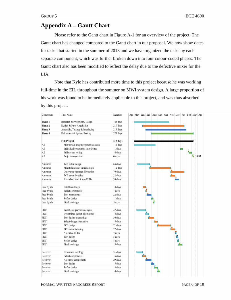
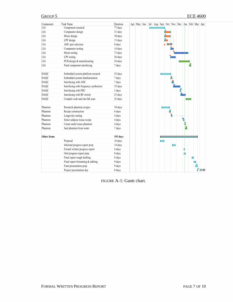
Appendix A – Gantt Chart
Please refer to the Gantt chart in Figure A-1 for an overview of the project. The
Gantt chart has changed compared to the Gantt chart in our proposal. We now show dates
for tasks that started in the summer of 2013 and we have organized the tasks by each
separate component, which was further broken down into four colour-coded phases. The
Gantt chart also has been modified to reflect the delay due to the defective mixer for the
LIA.
Note that Kyle has contributed more time to this project because he was working
full-time in the EIL throughout the summer on MWI system design. A large proportion of
his work was found to be immediately applicable to this project, and was thus absorbed
by this project.
GROUP 5 ECE 4600
FORMAL WRITTEN PROGRESS REPORT PAGE 7 OF 10
FIGURE A-1: Gantt chart.
GROUP 5 ECE 4600
FORMAL WRITTEN PROGRESS REPORT PAGE 8 OF 10
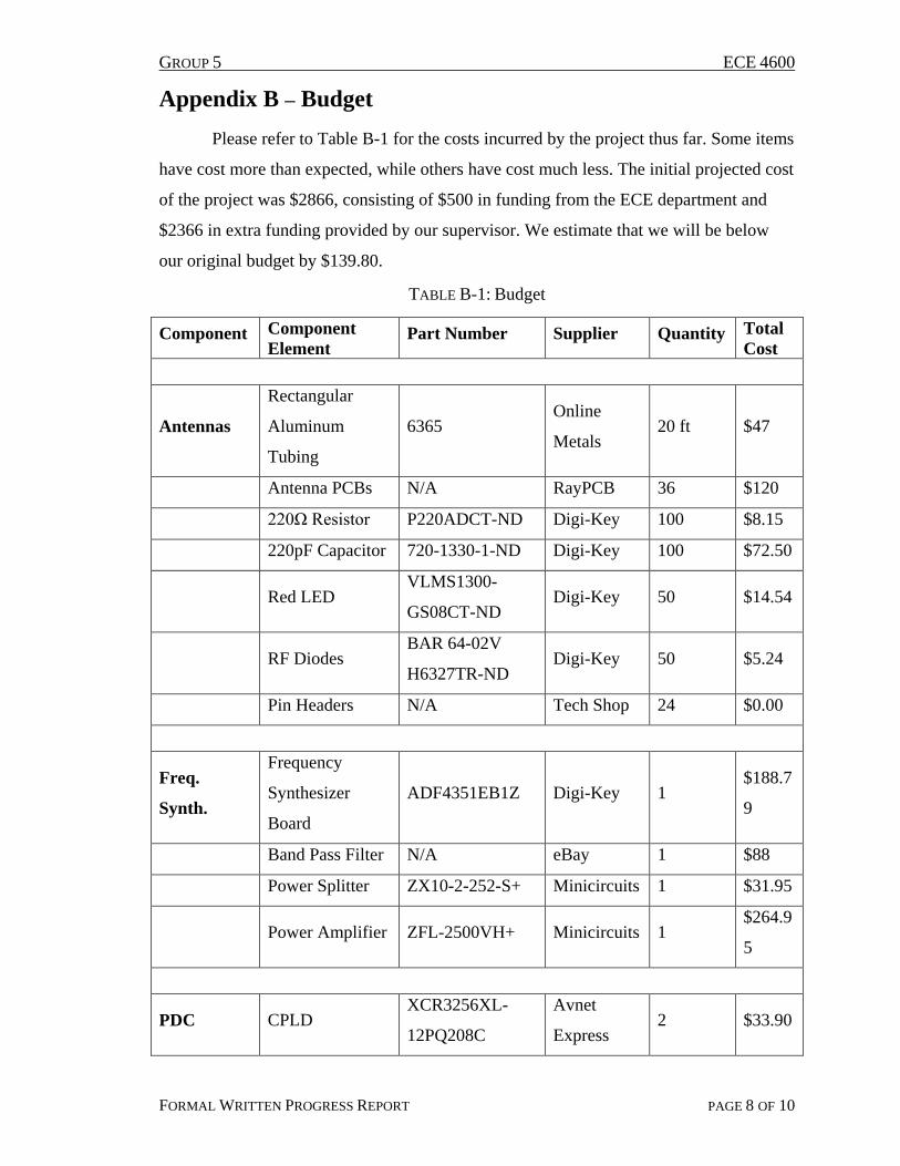
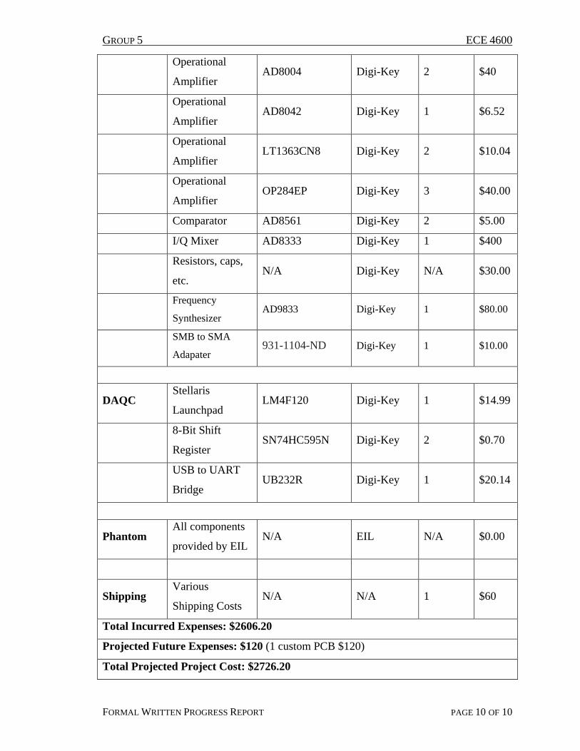
Appendix B – Budget
Please refer to Table B-1 for the costs incurred by the project thus far. Some items
have cost more than expected, while others have cost much less. The initial projected cost
of the project was $2866, consisting of $500 in funding from the ECE department and
$2366 in extra funding provided by our supervisor. We estimate that we will be below
our original budget by $139.80.
TABLE B-1: Budget
Component Component
Element Part Number Supplier Quantity Total
Cost
Antennas
Rectangular
Aluminum
Tubing
6365 Online
Metals 20 ft $47
Antenna PCBs N/A RayPCB 36 $120
220Ω Resistor P220ADCT-ND Digi-Key 100 $8.15
220pF Capacitor 720-1330-1-ND Digi-Key 100 $72.50
Red LED VLMS1300-
GS08CT-ND Digi-Key 50 $14.54
RF Diodes BAR 64-02V
H6327TR-ND Digi-Key 50 $5.24
Pin Headers N/A Tech Shop 24 $0.00
Freq.
Synth.
Frequency
Synthesizer
Board
ADF4351EB1Z Digi-Key 1 $188.7
9
Band Pass Filter N/A eBay 1 $88
Power Splitter ZX10-2-252-S+ Minicircuits 1 $31.95
Power Amplifier ZFL-2500VH+ Minicircuits 1 $264.9
5
PDC CPLD XCR3256XL-
12PQ208C
Avnet
Express 2 $33.90
GROUP 5 ECE 4600
FORMAL WRITTEN PROGRESS REPORT PAGE 9 OF 10
Voltage
Regulator
LM317MDTGOS
-ND Digi-Key 1 $0.79
220Ω Resistor P220FCT-ND Digi-Key 4 $0.48
360Ω Resistor P360FCT-ND Digi-Key 4 $0.48
1uF Capacitor 399-3678-1-ND Digi-Key 4 $1.52
0.1uF Capacitor 399-3676-1-ND Digi-Key 4 $1.68
Bussed 10kΩ
Resistors
4605X-101-
103LF Digi-Key 1 $0.32
CPLD PCB N/A RayPCB 2 $100
3.3V to 5V
Logic Converter
MC74HCT245A
DWGOS-ND Digi-Key 20 $12.10
Darlington
Transistor Chip
ULN2803AFWG
(CELHACT-ND) Digi-Key 20 $16.20
220Ω Chip
Resistor
SOMC220HCT-
ND Digi-Key 20 $22.00
BNC Connectors A101972-ND Digi-Key 5 $20.75
56pF Capacitors 490-3580-1-ND Digi-Key 100 $41.00
10uF Capacitors 490-3897-1-ND Digi-Key 100 $4.00
Probe Driver
PCB N/A RayPCB 1 $120
Ribbon Cable
Ends 2-1658527-0 Digi-Key 50
$126.7
3
12 Pin Ribbon
Cable N/A Tech Shop 144 ft $0.00
Pin Headers N/A Tech Shop N/A $0.00
Homodyne
Receiver
Low Noise
Amplifier ZX60-33LN-S+ Minicircuits 1 $79.95
I/Q Mixer ADL5382 Digi-Key 1 $215.7
7
LIA A/D Converter AD977A Digi-Key 5 $250
GROUP 5 ECE 4600
FORMAL WRITTEN PROGRESS REPORT PAGE 10 OF 10
Operational
Amplifier AD8004 Digi-Key 2 $40
Operational
Amplifier AD8042 Digi-Key 1 $6.52
Operational
Amplifier LT1363CN8 Digi-Key 2 $10.04
Operational
Amplifier OP284EP Digi-Key 3 $40.00
Comparator AD8561 Digi-Key 2 $5.00
I/Q Mixer AD8333 Digi-Key 1 $400
Resistors, caps,
etc. N/A Digi-Key N/A $30.00
Frequency
Synthesizer AD9833 Digi-Key 1 $80.00
SMB to SMA
Adapater 931-1104-ND Digi-Key 1 $10.00
DAQC Stellaris
Launchpad LM4F120 Digi-Key 1 $14.99
8-Bit Shift
Register SN74HC595N Digi-Key 2 $0.70
USB to UART
Bridge UB232R Digi-Key 1 $20.14
Phantom All components
provided by EIL N/A EIL N/A $0.00
Shipping Various
Shipping Costs N/A N/A 1 $60
Total Incurred Expenses: $2606.20
Projected Future Expenses: $120 (1 custom PCB $120)
Total Projected Project Cost: $2726.20