DESIGN OF A CLOCK AND DATA RECOVERY CIRCUIT IN …
57
DESIGN OF A CLOCK AND DATA RECOVERY CIRCUIT IN FDSOI TECHNOLOGY FOR HIGH SPEED SERIAL LINKS A Master Thesis Submitted to the Faculty of the Escola T` ecnica d’Enginyeria de Telecomunicaci´o de Barcelona Universitat Polit` ecnica de Catalunya by Hugo Ernesto Safadi Figueroa In partial fulfillment of the requirements for the degree in MASTER IN ELECTRONIC ENGINEERING Advisors: Diego Mateo Pe˜ na and Francesc Moll Echeto Barcelona, March 2021
Transcript of DESIGN OF A CLOCK AND DATA RECOVERY CIRCUIT IN …
DESIGN OF A CLOCK AND DATA RECOVERY CIRCUIT IN FDSOI
TECHNOLOGY FOR HIGH SPEED SERIAL LINKS
A Master ThesisSubmitted to the Faculty of the
Escola Tecnica d’Enginyeria de Telecomunicacio de BarcelonaUniversitat Politecnica de Catalunya
by
Hugo Ernesto Safadi Figueroa
In partial fulfillmentof the requirements for the degree in
MASTER IN ELECTRONIC ENGINEERING
Advisors: Diego Mateo Pena and Francesc Moll EchetoBarcelona, March 2021

Abstract
The purpose of this thesis is to design an 8 Gbps clock and data recovery circuit intendedto work in the receiver of a high-speed Serializer-Deserializer interface (SerDes). Theproposed architecture is based on a phase-locked loop operation (PLL) that integrates alinear phase detector, a charge pump, a wide-tuning range voltage-controlled ring oscillator(2.5- 12 GHz), and a third order low pass filter that achieves a bandwidth of 150 MHz. Awide loop bandwidth is considered in the design to achieve a high input jitter toleranceand a fast locking time. Implemented in 22 nm FDSOI, the overall circuit draws 1.38mWfrom a 0.8V power supply, exhibits a recovery clock RMS jitter of 0.970 fs and and requiresa locking time of 22 ns.
A Monte Carlo analysis has been performed applying temperature and voltage cornersof -40C to 125C and 0.72 V to 0.88 V respectively. The results indicated a 95.6%success rate. By using an external voltage that has been implemented to adjust the phasedetector’s flip-flops bias current, 100% success rate is achieved.
Keywords
CDR, PLL, FDSOI, VCO, jitter, phase noise.
2

Acknowledgements
I would like to thank my supervisors Diego Mateo and Francesc Moll, for all the help andsupport that they gave me during this work.
3

Revision history and approval record
Revision Date Purpose0 26/02/2021 Document creation1 01/03/2021 Document revision2 05/03/2021 Document revision
DOCUMENT DISTRIBUTION LIST
Name e-mailHugo Ernesto Safadi Figueroa [email protected] Mateo Pena [email protected] Moll Echeto [email protected]
Written by: Reviewed and approved by:Date 02/03/2021 Date 05/03/2021Name Hugo Ernesto Safadi Figueroa Name Francesc Moll i Diego MateoPosition Project Author Position Project Supervisors
4

Contents
List of Figures 6
List of Tables 7
1 Introduction 81.1 Project Background . . . . . . . . . . . . . . . . . . . . . . . . . . . . . . . 81.2 Organization . . . . . . . . . . . . . . . . . . . . . . . . . . . . . . . . . . 8
2 State of the art 92.1 Clock Recovery overview . . . . . . . . . . . . . . . . . . . . . . . . . . . . 9
3 PLL clock recovery architecture design 113.1 Clock recovery from a random data signal . . . . . . . . . . . . . . . . . . 113.2 CDR Phase detectors . . . . . . . . . . . . . . . . . . . . . . . . . . . . . . 12
3.2.1 Alexander (bang-bang) detector . . . . . . . . . . . . . . . . . . . . 133.2.2 Hogge detector . . . . . . . . . . . . . . . . . . . . . . . . . . . . . 13
3.3 Charge Pump . . . . . . . . . . . . . . . . . . . . . . . . . . . . . . . . . . 143.4 VCO . . . . . . . . . . . . . . . . . . . . . . . . . . . . . . . . . . . . . . . 16
3.4.1 Singled ended input- differential output ring oscillator . . . . . . . 183.5 CDR loop analysis . . . . . . . . . . . . . . . . . . . . . . . . . . . . . . . 193.6 Phase Noise and jitter . . . . . . . . . . . . . . . . . . . . . . . . . . . . . 233.7 Random jitter quantification . . . . . . . . . . . . . . . . . . . . . . . . . . 24
4 Circuit Design 264.1 Phase Detector . . . . . . . . . . . . . . . . . . . . . . . . . . . . . . . . . 264.2 Charge Pump . . . . . . . . . . . . . . . . . . . . . . . . . . . . . . . . . . 294.3 VCO . . . . . . . . . . . . . . . . . . . . . . . . . . . . . . . . . . . . . . . 31
4.3.1 Frequency tuning . . . . . . . . . . . . . . . . . . . . . . . . . . . . 334.3.2 Phase noise . . . . . . . . . . . . . . . . . . . . . . . . . . . . . . . 33
4.4 Control loop design . . . . . . . . . . . . . . . . . . . . . . . . . . . . . . . 344.4.1 Frequency and step response . . . . . . . . . . . . . . . . . . . . . . 37
5 Simulations and Results 395.1 CDR tracking . . . . . . . . . . . . . . . . . . . . . . . . . . . . . . . . . . 395.2 Phase noise and RMS random jitter measurement . . . . . . . . . . . . . . 40
5.2.1 Phase margin effect on noise and settling time . . . . . . . . . . . . 415.2.2 Phase detector gain trade-off with jitter and settling time . . . . . . 435.2.3 Transferred data input jitter . . . . . . . . . . . . . . . . . . . . . . 445.2.4 PRBS clock recovery . . . . . . . . . . . . . . . . . . . . . . . . . . 46
5.3 Monte Carlo simulation . . . . . . . . . . . . . . . . . . . . . . . . . . . . . 475.3.1 Power consumption . . . . . . . . . . . . . . . . . . . . . . . . . . . 49
6 Conclusions and future development 52
References 54
5

List of Figures
1 CDR block diagram . . . . . . . . . . . . . . . . . . . . . . . . . . . . . . . 92 NRZ encoding . . . . . . . . . . . . . . . . . . . . . . . . . . . . . . . . . . 113 Transmitted NRZ data power spectrum . . . . . . . . . . . . . . . . . . . . 124 Edge detection . . . . . . . . . . . . . . . . . . . . . . . . . . . . . . . . . 125 Alexander phase detector . . . . . . . . . . . . . . . . . . . . . . . . . . . . 136 Alexander detector truth table . . . . . . . . . . . . . . . . . . . . . . . . . 137 Hogge detector . . . . . . . . . . . . . . . . . . . . . . . . . . . . . . . . . 148 Charge pump . . . . . . . . . . . . . . . . . . . . . . . . . . . . . . . . . . 159 (a) Cascode configuration, (b) Gain boosted simplified topology, (c) Gain
boosted circuit . . . . . . . . . . . . . . . . . . . . . . . . . . . . . . . . . 1510 Gain-boosted Charge pump . . . . . . . . . . . . . . . . . . . . . . . . . . 1611 VCO Circuits . . . . . . . . . . . . . . . . . . . . . . . . . . . . . . . . . . 1712 Current starved ring oscillator . . . . . . . . . . . . . . . . . . . . . . . . . 1813 Single ended to differential phasors. . . . . . . . . . . . . . . . . . . . . . . 1914 Single ended to differential ring oscillator circuit. . . . . . . . . . . . . . . 1915 CDR linear model . . . . . . . . . . . . . . . . . . . . . . . . . . . . . . . . 2016 Second order Type 2 PLL bode plot . . . . . . . . . . . . . . . . . . . . . . 2117 Third order Type II PLL bode plot . . . . . . . . . . . . . . . . . . . . . . 2218 Plot of natural frequency over crossover point versus damping factor for a
Type 2 PLL . . . . . . . . . . . . . . . . . . . . . . . . . . . . . . . . . . . 2319 Random Jitter distribution . . . . . . . . . . . . . . . . . . . . . . . . . . . 2420 Folded CML D-latch circuit . . . . . . . . . . . . . . . . . . . . . . . . . . 2621 DFF with current source control implemented in Virtuoso Schematic Editor 2722 Latch Output peak to peak voltage in function of the current source values 2823 Hogge Detector circuit implemented in Virtuoso Schematic Editor . . . . . 2824 Clock Lagging the data signal . . . . . . . . . . . . . . . . . . . . . . . . . 2925 Charge Pump schematic and test-bench . . . . . . . . . . . . . . . . . . . . 3026 Charge pump DC Analysis . . . . . . . . . . . . . . . . . . . . . . . . . . . 3027 Open loop charge pump load capacitance voltage . . . . . . . . . . . . . . 3128 Ring oscillator single stage inverter with dummy load . . . . . . . . . . . . 3229 ROSC circuit schematic . . . . . . . . . . . . . . . . . . . . . . . . . . . . 3330 Ring oscillator phase noise at 8GHz . . . . . . . . . . . . . . . . . . . . . 3431 ROSC frequency range . . . . . . . . . . . . . . . . . . . . . . . . . . . . . 3532 ROSC 8GHz propagation delay . . . . . . . . . . . . . . . . . . . . . . . . 3533 Ring oscillator output differential signal simulation . . . . . . . . . . . . . 3634 CDR Linear Model in Simulink . . . . . . . . . . . . . . . . . . . . . . . . 3735 Open loop and closed loop frequency response . . . . . . . . . . . . . . . . 3736 System’s step response . . . . . . . . . . . . . . . . . . . . . . . . . . . . . 3837 CDR schematic . . . . . . . . . . . . . . . . . . . . . . . . . . . . . . . . . 3938 PLL tracking the clock signal of the input data . . . . . . . . . . . . . . . 4039 CDR frequency tracking period and steady state . . . . . . . . . . . . . . 4140 Clock phase noise . . . . . . . . . . . . . . . . . . . . . . . . . . . . . . . 4141 CDR transient response for increasingly phase margin . . . . . . . . . . . 4242 Clock phase noise for increasingly phase margin . . . . . . . . . . . . . . . 43
6

43 Clock phase noise in function of current gain . . . . . . . . . . . . . . . . 4444 Transient response for increasingly detector gain . . . . . . . . . . . . . . 4545 Phase noise transfered input jitter at BW=125 MHz . . . . . . . . . . . . 4646 PRBS data eyediagram and jitter . . . . . . . . . . . . . . . . . . . . . . . 4647 Clock recovery of PRBS stream . . . . . . . . . . . . . . . . . . . . . . . . 4748 CDR locked state of PRBS signal . . . . . . . . . . . . . . . . . . . . . . . 4849 PRBS clock eyediagram and jitter . . . . . . . . . . . . . . . . . . . . . . 4850 clock signal Monte Carlo . . . . . . . . . . . . . . . . . . . . . . . . . . . 4951 Monte Carlo steady-state best and worse cases . . . . . . . . . . . . . . . 5052 Monte Carlo settling best and worse cases . . . . . . . . . . . . . . . . . . 5053 Monte Carlo simulation at corner VDD=0.88V, T=125C where the clock
frequency goes beyond 8GHz. Vclatch is adjusted from (a) 700 mV to (b)500 mV . . . . . . . . . . . . . . . . . . . . . . . . . . . . . . . . . . . . . 51
54 Monte Carlo simulation at corner VDD=0.72V, T=-40C where the clockfrequency does not reach 8GHz. Vclatch is adjusted from (a) 700mV to (b)770 mV . . . . . . . . . . . . . . . . . . . . . . . . . . . . . . . . . . . . . 51
Listings
List of Tables
1 Comparison of CDR designs reported in literature . . . . . . . . . . . . . . 102 BER and RMS jitter multiplier factor . . . . . . . . . . . . . . . . . . . . . 253 Simulated phase noise of the ring oscillator . . . . . . . . . . . . . . . . . . 344 Loop filter calculated component values and frequencies . . . . . . . . . . . 365 CDR control loop parameters . . . . . . . . . . . . . . . . . . . . . . . . . 396 Phase margin and jitter trade-off . . . . . . . . . . . . . . . . . . . . . . . 437 Simulated phase noise and jitter values when current gain is reduced . . . . 448 Simulated clock RMS and peak to peak jitter(BER =10−12) applying a
input data with 0.01UI jitter . . . . . . . . . . . . . . . . . . . . . . . . . 459 Monte Carlo corner values . . . . . . . . . . . . . . . . . . . . . . . . . . . 4710 Current and power consumption for each block of the CDR . . . . . . . . 5011 Comparison of CDR designs reported in literature and this work . . . . . 52
7

1 Introduction
1.1 Project Background
This work is part of a current project, named DRAC and lead by the Barcelona Supercom-puting Center, which aims to develop a RISC-V microprocessor. Particularly, this workdeals with the design at schematic level of an analog PLL-based clock and data recoverycircuit that is expected to operate at the receiver of a high-speed serial interface to serveas a data transfer between the ASIC and an FPGA containing a DDR3 RAM interfacefor main memory access.
The CDR design takes into consideration the specifications of a serial link transmitterdeveloped in [1] that serializes 8 differential data inputs using an 8 GHz sampling clock.The transmitted data reaches a bit-rate of 8 Gbps with a maximum transmission fre-quency of 4 GHz. At the receiver, the CDR must recover the 8 GHz clock to achieve thedeserialization process.
A fully depleted silicon over insulator (FDSOI) 22 nm process [2] is employed for thisdesign. This technology is based on an ultra-thin insulator layer, called buried oxide(BOX) placed between the base silicon and the transistor thin-film channel. The buriedoxide minimize the parasitic capacitance between the drain and source and reduce thecurrent leakage due to the electron confinement inside the channel. This allows to achievehigh-speed operations with low power consumption and lower area occupancy.
1.2 Organization
This work is organized as follows:
Chapter 2 briefly overview the fundamentals blocks of an analog PLL-based CDR andpresents a compilation of reported designs found in literature, including their specifica-tions.
In Chapter 3 different architectures for the CDR blocks are discussed and chosen followingcertain design specifications relating the loop bandwidth, speed, noise performance, powerconsumption and area. A basic theory of jitter and phase noise is also introduced.
In Chapter 4 each of the CDR blocks are designed at transistor level and simulatedindividually in open loop situation. The loop filter components are designed and thelinear model for the control in open loop and closed loop is simulated using Matlab.
Finally, in Chapter 5 the operation of the closed loop control of the designed CDR issimulated. Some design parameters of the CDR blocks are adjusted to meet with thespecifications and a Monte Carlo analysis is performed to test the circuit for process andmismatch variations and validate the operation of the proposed design.
8

2 State of the art
2.1 Clock Recovery overview
A conventional PLL-based CDR is formed by the following components:
Figure 1: CDR block diagram
Phase detector (PD): It performs the data edge sampling usually employing flip flopsthat are synchronized by the reference local clock signal. It provides the phaseerror signal that controls the VCO frequency. There are two main approaches toimplement a phase detector [3]. The first uses a linear detector, where its outputpulses average is linearly proportional to the phase error between the data andthe clock. The second approach uses a sequential detector which produces a binaryoutput that contains the direction of the phase error excluding the magnitude.
Charge pump (CP): This block takes the phase error signal from the detector andconverts them into current pulses that are fed into the loop filter to charge ordischarge the capacitance of the filter, consequently providing the right controlledvoltage to lock the clock frequency.
Voltage-controlled oscillator (VCO): It generates the clock signal and provides thefrequency tuning range of the CDR. One common implementation is the ring os-cillator, formed by a chain of current-starved inverters in which the clock period isdetermined by the delay of each stage. This architecture is also called a voltage-controlled delay line and presents high stability, wide tuning range, and relativelylow jitter accumulation [4]. Other CDR implementations include LC tank oscillators[5]-[6] providing high frequencies operation but poor tuning.
Loop Filter: The loop filter, which is generally based on a low pass filter (LPF) providesthe stability to the control loop and noise attenuation for high-frequency harmonics.
The key parameters requirement in CDR includes the generation of jitter, power consump-tion, frequency range, input data jitter rejection capability and the input jitter tolerance.
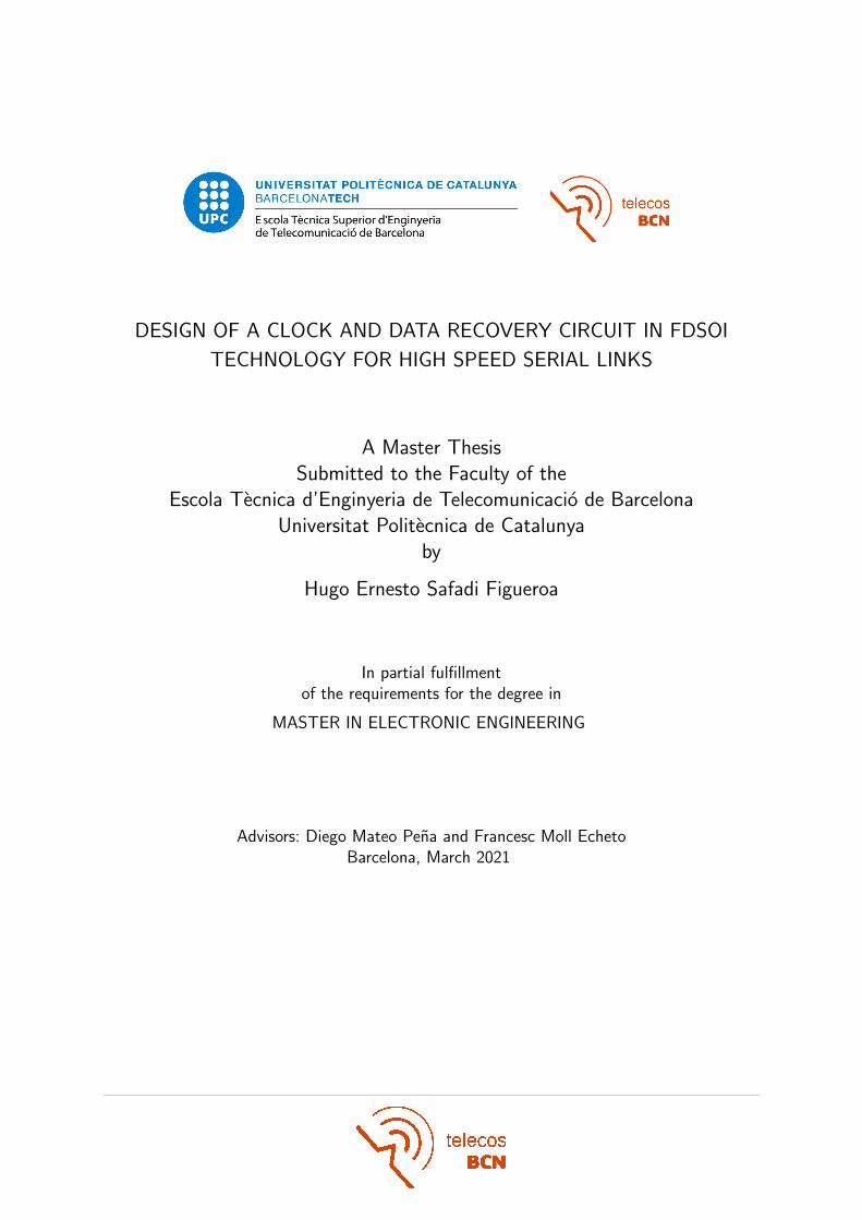
There are several CDR designs reported for high frequency applications with strict gen-erated jitter specification, for instance, a 1-16 Gbps all-digital CDR employing 65 nmCMOS process presented in [7] reported a clock jitter of 0.019 times the unit interval
9
(0.019 UI) and a power consumption of 80 mW. A CDR implementation employing 22nm SOI process has been reported in [8], intended to operate during NRZ/PAM4 decodingat 16 Gbps. This design presents a generated jitter of 1.92 ps at 8 GHz clock (0.03 UI). Ahigh jitter tolerance CDR design presented by Razavi in [9] works at 20 Gbps, reports aninput jitter tolerance of 2 UIpp at 5 MHz and a recovered clock generated jitter of 459 fssince it uses a wide bandwidth of 170 MHz. Table 1 summarizes some of the CDR designsreported with their specifications:
[7] [8] [9] [10]Technology 22 nm SOI 65 nm 65 nm 45 nm
Voltage supply 0.8 V 1.2 V 1 V 1 VData rate 16 Gbps 1-16 Gbps 20 Gbps 25 Gbps
Frequency tuning - 4-8 GHz 18.6-21.6GHz
12.25-13.59 GHz
Filter bandwidth - - 170 MHz 6 MHzClock RMS Jitter 0.03 UI 0.19 UI 0.018 UI 0.075 UIJitter Tolerance(BER=10−12)
- 0.2 UIpp 0.7 UIpp 0.3 UIpp
Power consumption 80 mW 87 mW 3 mW 4.97 mW
Table 1: Comparison of CDR designs reported in literature
For this work, the CDR is designed to have a wide frequency tuning range that allowsthe operation with multi-Gbps serial link protocols such as: Aurora 8b/10b [11], requiringbaud rates of 1.25Gbps, 2.5 Gbps and 3.25 Gbps; CEI-6G with baud rates from 4.9 Gbpsto 6.4 Gbps [12]; and CEI-11G, with baud rates from 9.9 Gbps to 11.2 Gbps [13].
The RMS jitter generated by the CDR should be around 0.01 UI (1 ps for 8GHz clock),following the PLL-CDR design criteria of [14].
Although other specification values are not initially defined, the desired performance char-acteristics for the CDR design also includes a fast locking time, high noise immunity thatensures a stable operation and a low power consumption.
10

3 PLL clock recovery architecture design
A clock recovery system implemented by a phase locked loop as depicted in Figure 1,synchronizes a self-generated reference clock signal with an input data bit stream by aunity negative feedback in order to extract its clock signal. It is conformed by a phasedetector, a charge pump, a loop filter and a VCO.
The design of the PLL-based clock recovery circuit meets with the following operationrequirements:
1. Detection of random bit sequences at the input by sampling each data transition.
2. Wide loop bandwidth to improve jitter tolerance.
3. Wide VCO frequency tuning.
4. Fast time response at locking the clock signal with minimum tracking error.
5. High local oscillator phase noise rejection
6. Low power consumption and efficient area occupancy.
3.1 Clock recovery from a random data signal
In most high-speed serial links, data is transmitted in a NRZ format which consists of apseudo-random binary sequence with a bit time equal to the clock period Tb = 1/fclk. Inthis type of encoding each bit has the same probability of being ‘0’ or ‘1’, therefore, itis possible to have a long pulse train of ‘1’ or ‘0’ making the clock detection difficult toachieve. The maximum signal frequency happens when the sequence is a series of alternat-ing ‘1’ and ‘0’ and is equal to half the clock frequency (fNRZmax = fclk/2), as is illustratedin Figure 2. This property allows data transmission using less channel bandwidth.
To illustrate the frequency properties of an NRZ signal, Figure 3 shows its frequencyspectrum in which it can be seen that the signal doesn’t carry energy at the fclk, neitherat its integer multiples frequencies. This property of the NRZ encoding has the drawbackthat it makes the PLL unable to track the clock signal. A non-linear transformation hasto be applied to the signal in order to generate the clock frequency. A differential operator(d/dt) doubles the pulse frequency by generating pulses in each transition of the signal.A squaring operation converts the signal in only positive pulses [15].
Figure 2: NRZ encoding
The phase detector of a CDR is capable of performing this operation by sampling thepositive and negative edges of the data signal using the reference clock from the VCO,
11

Figure 3: Transmitted NRZ data power spectrum
generating a pulse at each sample. Figure 4 shows the basic edge detection principle ina CDR consisting of a delay block that generates a version of the data signal delayedby a clock period Tb, an exclusive-OR gate compares the original data signal its delayedversion identifying each transition and generating a pulse at the output.
Figure 4: NRZ data edge detection
3.2 CDR Phase detectors
In PLL-based CDR there are two types of PDs: Non-linear (sequential) and linear detec-tors. In linear detectors, the pulse width of the output is proportional to the magnitudeof the phase error between the clock and the data, while non-linear detectors generate asequence of pulses with a fixed width that contains information about the direction of thephase error, but not the magnitude. The most common implementation for a non-lineardetector is the Alexander or bang-bang detector, while for linear detectors, the commonlyused implementation is the Hogge detector.
12

3.2.1 Alexander (bang-bang) detector
The Alexander phase detector (bang-bang) schematic is shown in Figure 5. It consists onfour D-flip flops that retime the data signal and two exlusive-OR gates that generates thepulses containing the phase error between clock and data. The output pulses T and Eindicate whether the clock is early or late to the data and change with each positive clockedge. The data can be sampled using the positive and negative edges of the clock, doublingthe sampling frequency. The decision making of the circuit requires a data sample at therising edge along with two previous samples. D-flip flop U1 provides the first data sampleon the rising data edge, U2 samples the previous data rising edge, while U4 provides thesample on the previous negative edge. The diference between the two outputs providesthe error phase information. Decision making is presented in truth table of Figure 6.
Figure 5: Alexander phase detector
Figure 6: Alexander detector truth table
3.2.2 Hogge detector
A Hogge detector is a linear phase detector that generates two output signals: A propor-tional signal with a varying-pulse-width (UP ) and a reference fixed pulse-width signal(DOWN).
The input data Din is connected to the D-flip flop (U1) and to the exclusive-OR gate(U2). U1 samples the data with the rising edge of the reference clock CK and generates a
13

delayed input signal D1. Din and D1 are compared by the exclusive-OR gate U2 producinga pulse waveform on each transition of the bit stream. The phase difference, which canbe represented as the position in which the clock samples the data determines the widthof the pulses, have a range that goes from 0 to TCK/2 when the clock is leading the datasignal and TCK/2 to TCK when the clock lags the data signal.
Figure 7: Hogge detector
A second D-flip flop (U3) synchronized by the inverted clock signal samples the delayedinput data D1 and generates D2. Since the phase difference between D1 and D2 will beone half of the clock period TCK/2, the second exclusive-OR gate (U4) will generate awaveform with a fixed TCK/2 pulse-width (DOWN) at each data transition, being thisthe reference signal regarding the varying pulse-width proportional signal.
Although non-linear detectors have good performance at high speeds, they occupy morearea and dissipate more power than linear detectors.
For this work, the Hogge linear detector is considered as it can work at the required speedalong with power and area efficiency. Moreover, a linear model for the control loop isplausible.
3.3 Charge Pump
A charge pump is a pull-up pull-down circuit that converts the pulses generated by thephase detector into current pulses that are fed by the loop filter capacitor whose outputvoltage controls the VCO.
One of the challenges in designing a charge pump circuit is the current mismatch thatis produced during the current switching due to the transconductance difference betweenthe NMOS and PMOS devices, along with the drain-source voltage differences generatedby the filter’s capacitor charge and discharge.
One approach to decrease current mismatches is by using a CMOS gain-boosted techniquethat increases the circuit’s output impedance using a cascode structure. Moreover, requireslow power dissipation and the bandwidth is not highly limited as it only uses one highgain amplification stage, which is suitable for high speed applications [16].
A cascoded structure formed by M1 and M2 is depicted in Figure 9.a where the outputimpedance across M1 drain is given by Rout = gm2r02r01. An amplification stage (A1) is
14

Figure 8: Charge pump
added to the circuit as it is shown in Figure 9.b where the transistor M1 is represented byits resistance r01. The M2 source node feeds the amplifier’s negative port while its outputfeeds the gate of M2. A1 amplifies and regulates Vx incurring in smaller deviations in theoutput current across M1 increasing the output impedance without staking more cascodedtransistors which maintains a low power consumption. The resultant output impedancefor this topology is Rout = gm2A1r02r01.
Figure 9: (a) Cascode configuration, (b) Gain boosted simplified topology, (c) Gain boosted circuit
An implementation for A1 is given by a NMOS transistor M3 biased by an ideal currentsource as is shown in Figure 9.c. The amplifier gain is A1 = −gm3r03 thus, Rout =gm2gm3r01r02r03.
Finally, the charge pump circuit is formed by two cascode gain boosted NMOS and PMOSamplifiers working complementary as depicted in Figure 10. The transistors M1, M2, M3
forms the negative feedback for PMOS path, while M4, M5, M6 forms negative feedbackfor NMOS path. The current sources driving M3 and M6 are formed by the current mirrorsM7 and M8.
15

Figure 10: Gain-boosted Charge pump (From reference [16])
3.4 VCO
The VCO is a key component for the CDR since it determines the operation frequencyof the CDR. Some design considerations have to be taken in order to adapt the CDRoperation requirements, among them: Low power consumption, wide frequency tuning(1 to 12 GHz), low area occupancy and low oscillation phase noise.
There are two types of VCO that are most commonly used for high speed applications:LC-tank oscillators and ring oscillators.
LC-tank oscillators are resonators based on inductor-capacitance networks with a highnoise rejection and low jitter. In addition, it has a high quality factor and hence, it canoperate at very high frequencies. However, it has a narrow frequency tune and occupieslarger area than a CMOS ring oscillator.
Ring oscillators (ROSC) are composed of a chain of an odd number of CMOS invertersthat relies its operation in the charge and discharge of the output loads at each stage. Theoutput frequency generated can be tuned by an amount of delay of each stage: decreasingthe stage delay would increase the frequency. A ring oscillator presents a higher phasenoise than LC oscillators, due to leakage current at the delay cells and high static leakagepower [17]. Nevertheless, ring oscillators are capable of a wide frequency tuning, low powerconsumption and less area occupancy than LC tanks.
There are several techniques that modify the ring oscillator frequency range performance,one of them is the current starved ring oscillator which is convenient to be implementedin CDR applications.
16

Figure 11: (a) Differential LC-tank oscillator, (b) Single-ended 3-stage ring oscillator
A current starved ring oscillator (CSROSC) employs current mirrors at each delay stageto control the current that charge and discharge the capacitive loads of each inverteroutput, thus controlling the delay of each stage. This configuration allows to have a widerand precise frequency tuning.
The control voltage acts as bias voltage for current mirror transistors which create avariable bias current for each stage that controls the frequency of oscillation, as is depictedin Figure 12. PMOS current mirror transistors P1, P3 and P5 operates as current sourceswhile the NMOS current mirror transistors N1, N3 and N5 operates as current sinks.
As mentioned before, the oscillation frequency is inversely proportional to the delay ofeach stage, the total delay of the oscillation will depend on the number of inverters in thering, thus the frequency can be defined as:
fo =1
NT(1)
Where N is the number of stages and T is the time delay.
The delay can be separated in charge time (t1) and discharge time (t2). If we defined Ctas the total load capacitance, I as the bias current, then we can define the oscillationfrequency as:
fo =1
N(t1 + t2)=
I
NCtVDD(2)
Where VDD is the supply voltage
17

Figure 12: Three-Stages Current starved ring oscillator
3.4.1 Singled ended input- differential output ring oscillator
As the input data coming from the transmission line is a differential signal, the phasedetector design considers differential D-flip flops. Hence, the clock signal generated by theVCO must be also differential. The advantages of working with differential topologies aretheir high rejection to common voltage noise, substrate and voltage supply noise, besidestheir low noise transfer to external circuits. However, a differential ROSC dissipates morepower, occupies a larger area and its output voltage swing is more limited than singleended circuits. Due to this trade-off, it is decided to maintain a single-ended configurationadapted to have a differential output. The technique used for this adaptation is proposedin [18]. To illustrate the operation principle of a single ended to differential converter, eachstage node waveforms can be approximated to sinusoidal signals in order to represent themas phasors as its illustrated in Figure 13. The phase difference between them is given byeach stage inverter phase shift and its propagation delay (π − φp). Assuming that thepropagation delay is same in each stage, these phasors are interpolated to generate tworesultant signals with the same amplitude and opposite direction.
Figure 14 shows the schematic of a five-stage differential output ring oscillator. A PMOSdifferential couple acts as a comparator and level shifter that generates the differentialrepresentation of the single ended signal Vo1 and Vo2. The inputs Vin1 and Vin2 are comingfrom the interpolated nodes through resistors R1 to R6. An additional inverter stage isshort-circuited to generate a half amplitude reference Vref.
Assuming that we used the same value for each resistor, interpolated voltages are repre-sented by:
Vin1 =1
3(Vp1 + Vp2 + Vp4) (3)
Vin2 =1
3(Vp3 + Vp5 + Vref ) (4)
18

Figure 13: Inverter stage phasors
Figure 14: Single ended to differential circuit
Combining equation (3) with the sinusoidal versions of each node phasor, Vin1 and Vin2
can be defined as:
Vin1 = Vref + Va sin(ωt) Vin2 = Vref − Va sin(ωt+ θ) (5)
3.5 CDR loop analysis
A linear model for a PLL-based CDR is depicted in Figure 15 where each component isexpressed in the frequency domain and the phase is the control variable.
The stability analysis of the system is given by the open loop transfer function betweenthe reference and input phase and is defined as:
T (s) =φout(s)
φin(s)=KpdKvco
sF (s) (6)
19

Figure 15: CDR linear model
Where Kpd and Kvco are the phase detector gain and the VCO gain respectively.
Since the VCO works as a linear voltage/frequency converter, taking the control voltagedefined by the phase error and adjusting its frequency oscillation proportionally to thephase, acts as an integrator, contributing with a pole at the origin.
The phase detector along with the charge pump transforms the phase error ∆φ from thedetector into current pulses Icp with proportional width following the expression:
∆t =∆φ
2πTck (7)
Where ∆t is the current pulse-width and Tck is the clock period.
If the loop filter is formed by a single capacitor Cp the relation between the increment involtage and the pulse-width ∆t is expressed as:
∆Vc =IcpCp
∆t =Icp∆φ
2πCpTck (8)
Assuming that the phase error occurs at t=0, for each period of time a linear approxima-tion is made to express Vc as a function of t as follows:
Vc(t) =Icpφ
2πCpu(t)t (9)
Where the unit step response u(t) = 1 at t ≥ 0.
The frequency domain transfer function of the voltage is obtained by doing the Laplacetransform over the derivative of dVc(t)/dt resulting in:
H(s) =Vc(s)
∆φ=
Icps2πCp
=Kpd
s(10)
We can obtain the current transfer function from Equation (10) defining the loop filterimpedance Z(s) = 1/sC:
20

I(s)
∆φ=Vc(s)
Z(s)=Icp2π
(11)
With a single capacitor the open loop transfer function contains two poles at the origin(Type II - 1st order PLL), making the system unstable since the phase angle will be -180
at the crossover frequency. Adding a resistor in series with the capacitor provides a zerolocated at ωz = 1/RpCp, stabilizing the control operation with a phase margin of 90 (seeFigure 16).
Modifying the current transfer function for a 2nd order RC filter we obtain:
I(s)
∆φ=Icp2π
Rp + sCpsCp
(12)
Figure 16: Second order Type two PLL loop filter (a) circuit schematic (b) frequency response
A 2nd order type II PLL presents significant drawback: each time the charge pump injectscurrent towards the R − Cp network, the control voltage (Vc) across Cp can’t changeinstantaneously at each charge and discharge due to the voltage drop in R, incurring involtage jumps, even during locked condition [19]. This jumpy effect is worsened with themismatch between the UP and DOWN current pulses. The resulting ripple creates largedeviations in the VCO frequency, and it increases the clock jitter. In order to reduce thateffect, a second capacitor C2 is connected in parallel to the R−Cp network, as is depictedin Figure 17, filtering the voltage ripple. Nevertheless, the drawback of adding a secondcapacitor is the addition of a third pole to the loop control, putting the system stabilityat risk, for this reason the components must be designed carefully.
Modifying the current transfer function for a 3rd order loop filter we obtain:
I(s)
∆φ=
Icp2πs(Cp + C2)
(1 + sωz
)
(1 + sωp
)(13)
21

Where the pole and zero frequencies are:
ωz =1
CpRp
(14)
ωp =Cp + C2
CpC2Rp
(15)
Thus, the open loop transfer function for a third order-type two PLL is defined as:
T (s) =KpdKvco
s(Cp + C2)
(1 + sωz
)
(1 + sωp
)(16)
The bode plots are shown in Figure 17: the 0-dB crossover frequency is placed between thezero, located at lower frequencies, and the pole, located at higher frequencies in order tohave enough phase margin. A distance ”k” factor between the pole and the zero frequencies
(k =√
ωp
ωz) can be related with the phase margin φPM following an approximation for
third order PLL defined in [20]-[21] :
k =
[1 + sin(φPM)
1− sin(φPM)
] 12
(17)
Figure 17: Third order Type two PLL loop filter (a) circuit schematic (b) frequency response
Another parameter to be analyzed is the damping factor represented by ξ. This parameteris useful to set the settling time of the frequency step response and the stability of thesystem. ξ can be determined by the relation between resonance frequency and the 0-dBcrossover frequency which can be approximated through a mathematical model presentedin [15] for type II PLLs which describes the curve depicted in Figure 18 where the reso-nance frequency fn normalized to a crossover frequency f0dB versus the damping factor
22

ξ is plotted. From the curve, we can deduce that when the resonance and crossover fre-quency are close to each other, the damping ratio decreases, and therefore the frequencyresponse will present more oscillations before the steady-state, increasing the settling timeand worsen the stability of the control (shorter phase margin). On the other hand, thefurther apart these frequencies are between them, the damping ratio is increased, stabi-lizing the system (larger phase margin) and decreasing the settling time. Nevertheless,an overdamped system (values from 0.8 to 1.5) degrades the optimum control speed to aslower response [22].
Figure 18: Plot of natural frequency over crossover point versus damping factor for a Type II PLL(from reference [15])
For third order PLLs the damping ratio can be approximated as it is shown in [23] :
ξ =− lnMp√
lnMp2 + π2
(18)
Where Mp is the step response’s overshoot at the peak magnitude.
In PLL applications the loop filter used can be either active or passive. For clock recoveryapplications it is more convenient to use a passive filter as it generates less jitter due tothe fact that the noise it contributes is only thermal due to the components. In an activefilter, in addition to thermal noise, the flicker noise (1/f) of the transistors increases withthe gain of the circuit [24].
3.6 Phase Noise and jitter
Considering the spectral density of a signal modulated periodically in frequency, thephase noise is defined as the signal’s sideband power in a 1-Hertz bandwidth at a certainfrequency offset from the signal’s carrier frequency. We can refer the signal side-bandas the noise power density. In the time domain the phase noise is represented as fast,short term fluctuations on the periodicity of the waveform, commonly called jitter. These
23

deviation on the PLL-CDR output signal’s phase can be caused by self-generated randomand deterministic noise sources and by external noise present in the input data signal.
In clock recovery loops the output clock jitter is produced by the ripple in the controlvoltage for the VCO caused by current mismatches in the charge-pump, the fluctuationson the power supply lines, edge detection errors produced in the PD, the noise generatedby the substrate and so on. All these noise sources are considered deterministic sincetheir origin is located in the circuit. In addition, there are random fluctuations whichmore difficult to determine. An example of this can be the thermal noise generated byactive components on the circuit.
Another jitter source that the CDR needs to deal with is found in the input data signalas it is transmitted by a noisy medium before arriving to the receiver. The jitter embed-ded in the input contains several frequency components, producing slow and fast phasedeviations. CDRs with narrowband loop filters will reject the high frequency componentof the input data. This property is called jitter transfer, representing the amount of jittercapable of being suppressed by the clock recovery. A good jitter transfer will produce a“clean” clock output.
Another effect to consider is the CDR’s jitter tolerance. As the low frequency componentsare not suppressed, some of the input jitter is inherited by the output clock. When sam-pling the data edges in the phase detector the clock keeps up with the input data as theyshare the same jitter, this maintain a certain stability in the system by not incurring infalse detections. However, for a narrowband CDR high frequency jitter is not transferredto the recovered clock which can incur in false edge detections. Having a wideband loopfilter increases the maximum amount of input jitter that can be tolerated by the CDRbefore incurring in detection errors.
3.7 Random jitter quantification
The random periodic jitter (RJc), given by uncorrelated noise sources, defines the vari-ations of the periodic signal from its mean value. As the number of period samples in-creases, the jitter value tends to increase following a normal distribution curve as is shownin Figure 19.
Figure 19: Random jitter distribution. σ= RMS value.
24

The RMS jitter (RJRMS) represents 1σ deviation of the probability distribution, whichoccupies around 34.1% of the jitter samples, counting from each side of the mean value µ.The the peak to peak jitter Jpp value represents the 100% of the normal curve. However, itis an unbounded value since it may increase with the number of jitter samples. Therefore, itis necessary to establish a range according to a system bit error rate (BER) specification.This gives the total jitter budget of the CDR, where any sample that falls out of therequired range will incur in a bit error. The wider the jitter range, the more tolerancethe CDR shows to the various random jitter source in a communication link. In highspeed SerDes links, a usual BER of 10−12 is required, meaning that, in order to obtain themaximum jitter budget it is necessary, in principle, to sample 1012 clock periods. However,it is possible to approximate the jitter value by employing a factor that multiplies thesigma at each side of the mean value (±Nσ) according to the BER specification [25]. Asit is shown in Table 2 :
BER N10−3 6.1810−6 9.50710−9 11.99610−12 14.698
Table 2: BER and RMS jitter multiplier factor
The RMS and the peak to peak values are usually expressed as a fraction of a data bitstream unit interval (UI), which is generally equal to the bit time.
25

4 Circuit Design
This chapter presents the design process of the CDR by describing the operation of eachcomponent circuit and showing its isolated behavior. The simulations are done employingthe Cadence ADE simulator. For the control modeling, Matlab-Simulink is employed togenerate the frequency and step response of a third-order second type PLL control. Allthe designs are made considering the FDSOI flipped well architecture [26].
4.1 Phase Detector
The Hogge detector is implemented using two differential D flip-flops based on currentmode logic D-latches proposed in [27]. This design allows the flip-flop to operate at voltageslower than 1 V since its folded topology uses fewer stacked transistors. Moreover, it hasa good performance at high frequencies and low power consumption. Figure 20 showsa folded CML latch. The clock signal is connected to the PMOS differential pair M1-M2 driving a current Iss towards the current mirrors formed by transistors M7-M9 andM8-M10. The NMOS pair M3-M4 samples a data bit while the couple M5-M6 holds thedata bit since their gates are cross-connected with M3-M4, creating positive feedback. Theloads represented by RD determines the voltage swing at the drain nodes of the NMOStransistors.
Figure 20: Folded CML D-latch circuit [27]
As it shown in [28] the minimum voltage supply for this topology can be defined as:
VDDmin =Vswing
4+ VTH + 2VOV (19)
Where Vswing is the peak to peak output voltage:
Vswing = 2ISSRD (20)
VTH and VOV are the transistor’s threshold voltages and overdrive voltages respectively.
26

In FDSOI 22nm technology with a flipped-well body bias architecture, VTH value is around0.25 V while the supply voltage is 0.8 V. To preserve a good performance of the latch,the swing voltage should be set around 0.5 V [28].
In order to design a master-slave D-flip flop from the CML latch, two folded latches canbe combined by sharing the clock PMOS differential pair as depicted in Figure 21.
The latch current source is designed using a multiple current mirror circuit controlled byan external voltage pin Vclatch that allows us to control the latch voltage swing and hence,to adjust the sampling speed and power dissipation during the CDR circuit testing.
Figure 21: Master-slave DFF with current source control implemented in Virtuoso Schematic Editor
Figure 22 shows the DFF operation with different Vclatch voltages: 0.6, 0.7 and 0.8 V aswell as different generated ISS current values: 47.6 µA, 61.6 µA and 71.4 µA. For thissimulation RD was set with 12 kΩ. It can be seen that the voltage swing increases alongwith ISS, going from 0.49 V to 0.6 V. Within this range the flip flop can operate correctly.
The glitches at the output Q0 are generated during the differential clock switching whereboth signals coincide at a common voltage that does not reach the PMOS differential pairthreshold, which implies a drop in the current that feeds the current mirror transistors.Consequently, the drain voltage of the NMOS that receive the data pulses tends to risetowards VDD. However, since the clock signal crossovers happens in a short period of timethe NMOS drain voltage’s surges are not high enough to alter the operation of the circuit.
Figure 23 shows the implementation in Cadence of the Hogge detector schematic previ-ously depicted in Figure 7.
The voltage applied on the Vclatch external pin is 0.75 V resulting in VQo1peak−peak= 0.57V and a ISS = 61.6 µA.
27

Figure 22: Latch Output peak to peak voltage in function of the current source values
To simulate the pulse-width variation of the output signals UP and DOWN due to thephase error between the input data and the reference clock, a periodic pulse waveformwith a period of TData=250 ps is phase-shifted from the clock signal who has half of thedata period TCK=125 ps.
Figure 24 shows the UP pulse-width variations in proportion to the magnitude and direc-tion of phase error, while DOWN pulses is used as reference and maintains a fixed pulsewidth equals to TCK/2.
When the data signal leads the clock by 20 ps (-0.16π phase shift) the pulse-width ofthe UP output decreases to Tck/2 - 20 ps = 42.5 ps as it shows Figure 24.a. This leadsthe charge pump to decrease the charging periods of the loop filter’s capacitor and con-
Figure 23: Hogge Detector circuit implemented in Virtuoso Schematic Editor
28

Figure 24: (a) Data signal leads the clock by 20 ps , (b) Data signal lags the clock signal by 20 ps
sequently, it decreases the control voltage which slows down the clock frequency until thephase difference is corrected.
In the other case shown in figure 24.b, the data signal lags the clock signal by 20 ps(+0.16π phase shift), the UP output will increase to Tck/2 + 20 ps= 82.5 ps. Now, thecharging times longer than discharges, which increases the control voltage and hence,speeds up the clock frequency until it reaches the data phase.
These open loop simulations of the designed phase detector describes the operation whenthere are small phase shifts between the data input and the reference, which is equivalentto the locked state of the PLL in closed loop. However, during the frequency trackingperiod, the Hogge detector works as a frequency detector, and depending on the designsettings, one of the possible drawbacks is the detection of harmonics of the target fre-quency. This can occur due to several causes: distortions on the output signal of thelatch, noise coupled from the supply lines or substrate lines or slow risings are fallingedges which incurs in failed edges samples.
In closed loop operation, which is analyzed in Chapter 5, these errors can be mitigatedby adjusting the Iss current employing the external control voltage Vclatch.
4.2 Charge Pump
Figure 25 shows the schematic for the proposed CDR’s charge pump based on a cascodegain-boosted topology. The phase detector’s UP signal is connected to the gate of tran-sistor P1, while DOWN is connected to the gate of N1. When UP pulses come out fromthe detector, P1 starts steering a current towards the loop filter capacitor, charging it.DOWN pulses out from the detector turn on the transistor N1, allowing the capacitorto discharge. The single-stage amplifier P2 along with P5 form the gain-boosted circuitthat increases the output impedance and hence, improving the current matching as was
29

described in the previous chapter. The current sources for the amplification stage areformed by P0-P3 and N0-N4 current mirrors.
Figure 25: (a) Charge-Pump schematic circuit, (b) block Test-bench
Figure 26 shows the DC simulation of the charge pump output currents sweeping theoutput voltage from 0 to 800 mV. The width of the transistors P1, P5, N1, N3 are adjustedto generate a maximum charge and discharge current of 70 µA, which will decrease duringthe voltage swept until both currents intercept at 67 µA, when the output is 420 mV,which is the steady-state voltage in open loop.
Figure 26: DC simulation of the charge pump output currents
The operation of the charge pump is tested in open loop by connecting two periodic8GHz signals in phase with each other and with a 50% duty cycle, simulating the UPand DOWN pulses of the phase detector. A load capacitance of 2.2 pF is connected atthe output.
By setting the initial condition of the capacitor voltage to 0 V, the PMOS path willstarts injecting current into the load until it reaches a threshold voltage of 420 mV as it
30

is depicted in Figure 27.a. At that instant, the NMOS path start draining current fromthe capacitor during the discharge periods. As the difference between the charge anddischarge currents approaches zero, the output voltage will begin to reach steady statevalue at around 0.6 µs. Figure 27.b. shows the steady-state from 0.698 µs to 0.7 µs, thevoltage across the capacitor presents a ripple due to the charge and discharge periodswith peak to peak magnitude that reaches 2 mV.
Figure 27: (a) Open loop charge pump load capacitance voltage (b) Voltage ripple in steady state
The amplitude of the output voltage ripple depends on the frequency of the input pulses,its capacitive load and the output currents, following the equation:
∆V =IL∆t
CL(21)
Where IL is the current flowing through the load, ∆t is the charge and discharge perioddetermined by the UP and DOWN pulse-width and CL is the output capacitance. Itis convenient to have a low ripple at the output considering that in closed loop, thefeedback control take place on the CDR and the voltage ripple will generate variationsin the output frequency, and depending on the sensitivity of the VCO, this ripple canbe significant at the accumulation of jitter. Higher currents will generate a larger ripple,and hence, more frequency variations. Nevertheless, it will reach the target voltage faster(shorter settling time). On the other hand, smaller currents will produce less frequencyvariations, improving the output jitter but it will take a longer time to reach the PLLsteady state (longer settling time).
4.3 VCO
A current starved five-stage ring oscillator with differential output is designed to have awide frequency tuning range and low phase noise, following the CDR requirements. Fig-
31

ure 28 presents a single inverter stage for the ROSC. The current starved VCO allows thecontrol of the propagation delay due to the charge and discharge of the gate capacitanceof each inverter’s output by adjusting the bias voltage of current source transistor P1 andthe current sink transistor N2. The devices were designed to provide a fixed current of100 µA at each stage. An inverter dummy load is connected at the output to have a loadsymmetry for all stages.
Figure 28: Ring oscillator single stage inverter with dummy load
As was mentioned in the previous chapter, a single-ended with differential output config-uration its considered for the ring oscillator circuit. Figure 29 shows the final schematicmade in the Cadence editor. The resistances that form the interpolating network are setto 11.5k Ω, while the load resistance of the PMOS differential pair which determines theoutput voltage swing is set to 20k Ω. The bias voltage of the differential circuit’s currentsource is controlled by a PMOS current mirror that generates a 90 µA bias current. Finally,the differential output Vo1 and V02 are connected to CMOS inverter buffers which drivesa larger capacitive load that increases the voltage swing and minimizes the propagationdelay.
Figure 33 depicts the ring oscillator differential output signals simulation. The common-mode voltage reference Vref is not constant since each inverter node signal is not exactlysinusoidal as it was approximated in theory. This implies small variations on the interpo-lated signals Vin1 and Vin2. Nevertheless, the output voltage presents good symmetry anda large voltage swing, around 0.65 V. Finally, the output buffers are made by two CMOSinverters to amplify the output signals, generating the output clock signals.
32

Figure 29: Ring oscillator circuit schematic
4.3.1 Frequency tuning
Figure 31 shows the VCO transfer function plot simulation. The linear region obtained inthe simulation determines the frequency tuning range, going from 2.5 GHz to 11.5 GHz.The control voltage range goes from 250 mV to 400 mV. The linear factor of this regiondescribing the VCO gain is calculated by the slope of the line ∆f/∆V = 70 GHz/V.
The required oscillation frequency for synchronizing the clock is generated with 340 mVcontrol voltage. Figure 32 shows the propagation delay between two oscillator’s internalnode signals oscillating at 8 GHz, which was found to be tp =12.37 ps.
4.3.2 Phase noise
ROSC phase noise is generated mostly by the slow rising and falling edges at the nodesof each inverter, increasing the jitter, the sensitivity to supply voltage variations, anddifficulties to maintain a 50% duty cycle. However, this effect can be minimized by resizingthe current starved transistors which control the speed of the rising and falling edges. Theincrease of current injected by the current mirrors speed up the charge and discharge ofeach inverter node, improving the jitter. Nevertheless, the power consumption area alsoincreases. In Figure 30, the simulation of the phase noise generated by the proposedfive-stage current starved ring oscillator is shown.
The measured phase-noise shows a slope of about 30-dB/dec at lower frequencies, pro-duced by flicker noise (1/f noise) [15]. A break point offset frequency at around 10 MHz(flicker corner frequency) drops the slope from 30 to 20-dB/dec until the curve flattens ataround 8 GHz defining the thermal white noise produced in the oscillator.
The jitter value, calculated from the phase noise plot within the integration limits from1K to 10GHz, gives a value of 0.3ps RMS.
33

Figure 30: Ring oscillator phase noise at f=8 GHz
Offset Phase Noise(dBc/Hz)100kHz -321MHz -62.510MHz -88.6100MHz -112
Table 3: Simulated phase noise of the ring oscillator
4.4 Control loop design
For the design of a linear control model for a third-order, type two PLL-CDR the followingprocess is considered:
1. Selection of the 0-dB crossover frequency of the system and the required phasemargin φPM , following the design criteria of chapter 3.
2. Obtaining the k factor derived from the phase margin, employing the Equation (17)in order to estimate the distance between ωz and ωp.
3. Estimation of the filter component’s values using the open loop transfer functionT (s).
As a first attempt, we set the crossover frequency (f0−dB) at 100MHz to have wide band-width that allows the CDR to have a high jitter tolerance and fast signal tracking. How-ever, this value is adjusted according to the phase noise simulations in chapter 5.
For the phase margin we define 35, following the design criteria of [29] that suggests thatfor PLL applications, phase margins greater than 30 ensure a stable operation. From thedefined phase, the pole and zero frequencies can be located using as reference the k factor
34

Figure 31: Ring oscillator frequency tuning range
Figure 32: Propagation delay of one ring stage oscillating at fo=8 GHz
estimated in Equation (17). Giving a value of 1.92.
In order to obtain the filter’s component values, it is assumed that the crossover frequencyis located between the zero and pole to ensure the desired phase margin: ωz < ωc < ωp.Then, the magnitude of the open loop gain T (s) is evaluated at the crossover frequency,|T (jωc)|=1 as follows:
|T (jωc)| =IcpKvco
2π(Cp + C2)ω2c
√1 + (ωcRpCp)2√1 + (ωc/ωp)2
= 1 (22)
Since Cp + C2 ≈ Cp:
|T (jωc)| ≈IcpKvco
2πCp
√(ωcRpCp)2
ω2c
≈ IcpKvcoRp
2πωc= 1 (23)
35

Figure 33: Ring oscillator output differential signal simulation
From previous analysis of the phase detector gain (Kpd), and the VCO gain (Kvco) wereobtained:
Kpd = Icp2π
= 10.8µA/rad
Kvco = ∆V∆f
= 7x10¹⁰Hz/V
By calculating Rp from Equation (22) and if Cp is set arbitrary to an initial value of 2.2
pF we can calculate C2 relating equation (14) with k =√
wp
wzas follows:
C2 =Cp
k2 − 1(24)
Then, the zero and pole frequencies are calculated employing equations (14) and (15).
Table 4 summarizes the calculated filter components and the obtained frequencies:
Cp 2.2 pFC2 0.77 pFRp 1 kΩfc 100 MHzfz 70.4 MHzfp 211 MHz
Table 4: Loop filter calculated component values and frequencies
36

4.4.1 Frequency and step response
Given the parameters obtained from the equations of the 3rd order filter, a linear modelis created in Matlab employing the open loop transfer function T (s) to simulate thefrequency and step response of the loop control as it is shown in Figure 34.
Figure 34: CDR Linear Model in Simulink
Figure 35 (a) and (b) depicts the magnitude and phase bode plots for open loop andclosed loop operation respectively. The resonance frequency is located at about 80 MHz,which represents 0.8 times the crossover frequency, resulting in a damping factor around0.4 (according to the curve of Figure 18)
Figure 35: Frequency response simulation for (a) open loop, (b) closed loop
The step response presented in Figure 36 gives information about the settling time and
37

overshoot at the resonance frequency. This parameters are described by the damping ratioξ and it depends on the phase margin.
Figure 36: System’s step response Matlab simulation
For a 35 degree phase margin the simulation’s results shows an overshoot of 53% andsettling time of 19.3 ns. The damping ratio is calculated employing Equation (17) whichgives a value of 0.4, corroborating the previous estimation from the fn/f0 vs ξ curve.
In summary, the linear model defined in this chapter is intended to have a fast trackingoperation, keeping the control stability with an underdamped loop control. However, inthe next chapter, this theoretical model is simulated and the trade-offs between the phasemargin, settling time, area occupancy and noise performance will be analyzed, incurringin the adjustment of the filter parameters to improve the system.
38

5 Simulations and Results
In this chapter, the closed-loop control of the proposed CDR circuit shown in Figure 37 isverified by applying two types of input data signals: a 4 GHz pulse wave with 50% dutycycle and a pseudo-random bit sequence (PRBS) with a bit rate of 8 Gbps. The simulationresults are focused on the analysis of the settling time, the recovered clock phase noise,and the data input jitter rejection capability under different loop bandwidths. Circuitdesign adjustments are implemented in order to have a generated RMS jitter in the clockless than 1 ps (0.016UI) and an input tolerance jitter of at least 0.24 UIpp of the datasignal. Finally, a Monte Carlo simulation is performed to test the circuit under processvariation and mismatches.
The initial parameters of the CDR control loop are summarized in Table 5:
Bandwidth 122 MHzPhase margin 35
Detector gain 10.8 µA/radVCO gain 70 GHz/VTarget frequency 8 GHz
Table 5: CDR control loop parameters
Figure 37: CDR schematic implemented in Cadence
5.1 CDR tracking
Figure 38 shows the CDR frequency tracking response of a 4 GHz input pulse-wave with a50% duty cycle. An initial condition for the simulation is established by setting the voltageat the filter’s capacitance node (Vosc) to 0.25 V, which is the threshold voltage that drives
39

the ring oscillator’s current starved transistors, starting up the 3 GHz clock frequencythat feeds the input and samples the edges of the data signal pulses. The Hogge detectorproduces the phase error signals (UP and DOWN) between the sampled data edges andthe reference clock. Subsequently, the charge pump converts the error signals into currentpulses that adjust the charge of the filter’s capacitance increasing the control voltage untilthe oscillator reach the 8 GHz target frequency at 347 mV. The CDR recovers the clockfrequency, requiring a settling time of approximately 30 ns.
Figure 38: CDR frequency tracking
Figure 39.a shows the CDR tracking period, where the detector’s DOWN signal keepsa reference pulse-width equals to the clock’s half period, producing a 68 µA dischargecurrent, while the UP signal varies its pulse-width adjusting the charge current. When theCDR locks the clock frequency, the charge and discharge pulses are balanced, producinga 136 µA peak to peak current pulse-wave that flows through the loop filter. The filter’scapacitance generates a control voltage peak to peak amplitude of 5 mV, leading to anoutput frequency steady-state error of ∆fclock =1 MHz as it shows in Figure 39.b Toquantify the amount of jitter due this frequency variations at the locked state (amongother noise sources), phase noise simulations are performed in the following section.
5.2 Phase noise and RMS random jitter measurement
Since the input data stream is an ideal signal with no jitter, we can obtain the clockphase noise generated exclusively by the CDR circuit, where the factors that contribute
40

Figure 39: (a) Phase error pulses during the frequency tracking, (b) CDR during the locked state
predominantly to the noise generation are the phase deviations between the internal nodesof the ring oscillator, the amplitude of the ripple in the control voltage given by the chargepump current, the variations in the power and ground lines and the loop filter’s bandwidth.
Figure 40 shows the 8 GHz clock signal’s phase noise giving a value of -114 dBc/Hz at10 MHz offset frequency. By using the ADE PNoise analysis and considering a frequencyrange from 10 KHz to 10 GHz, a 1.14 ps RMS jitter is obtained.
Figure 40: Output clock phase noise
5.2.1 Phase margin effect on noise and settling time
By increasing the phase margin, the damping ratio of the transient response increases.Hence, the settling time shortens as it is shown in Figure 41. Moreover, a larger marginimplies a wider separation between the pole and zero frequencies. When the pole is shifted
41

to higher frequencies, its distance from the natural frequency widens and the noise over-shoot decreases as it is shown in Figure 42. Nevertheless, the filter noise bandwidth is alsoincreased, allowing higher frequencies noise sources to be transferred to the output clock.The resulting jitter, settling time and filter components dimensions are summarized inTable 6.
Figure 41: CDR transient response for increasingly phase margin
In summary, larger phase margins improves the CDR tracking speed and control stabi-lization as the noise bandwidth increases (higher noise immunity). The drawback is theaddition of generated jitter in the output clock. Particularly, setting the phase marginto 55 the clock jitter is increased up to 1.20ps (0.02UI) and the settling time decreasesfrom 30ns to 11.6ns which is reasonable operation trade-off. However, one approach to
42

Figure 42: Clock phase noise for increasingly phase margin
φPM Settling time RJRMS R C2 Cp35 30 ns 1.14 ps 1.2KΩ 0.77 pF 2.2 pF45 27 ns 1.16 ps 1.2KΩ 0.65 pF 2.5 pF55 11.6 ns 1.20 ps 1.2 KΩ 0.5 pF 2.8 pF65 11 ns 1.25 ps 1.2 KΩ 0.1 pF 3 pF
Table 6: Phase margin and jitter trade-off
reduce the generated jitter without slowing significantly the CDR tracking speed is bymoderately reducing the phase detector gain.
5.2.2 Phase detector gain trade-off with jitter and settling time
The trade-off between phase detector gain over the clock jitter relies on the fact thatlowering Kpd the control voltage ripple reduces along with the clock frequency deviations,reducing the generated jitter. Nevertheless, the settling time, as it was mentioned inthe chapter 5, is increased since that with less charge injection, maintaining the samecharge/discharge periods, the capacitor’s charge will take more time to reach the voltagethat locks the target frequency.
In the following simulations, the charge/discharge currents are dropped from 68 µA to 40µA (Kpd from 10.8 µA/rad to 6.4 µA/rad), leading to a phase noise reduction of 4 dB overthe frequency range until the control loop crossover frequency as depicted in Figure 43and a lightly slower frequency tracking with a settling time of 12.6 ns as Figure 44 shows.
Table 7 summarizes the generated jitter and settling time trade-off as the current is
43

Figure 43: Clock phase noise in function of the current gain
decreased:
[IcpµA] φPM Kpd Phase noise@10MHz RJRMS Settling time68 µA 55 10.8 µA/rad -114 dBc/Hz 1.20 ps 11.6ns40 µA 55 6.4 µA/rad -118 dBc/Hz 970 fs 12.2ns
Table 7: Simulated phase noise and jitter values when current gain is reduced
The generated jitter in the recovered clock jitter could be reduced down to 970 fs (0.015UI) lowering the current to 6.4 µA/rad. The settling time increases to 12.2 ns whichdoesn’t affect significantly the CDR tracking speed.
Now, we will take into consideration the transfer of the input jitter to the output clock,where the design trade-off will rely on the input rejection towards the input tolerance.
5.2.3 Transferred data input jitter
To observe the CDR input jitter rejection capability, the input pulse wave is distortedwith a 0.08 UI jitter (10 ps RMS).
Figure 45 shows the input data noise rejection tested for loop 3 dB cutoff frequenciesof 70 MHz, 122 MHz and 150 MHz (maintaining a 55 phase margin) within the offsetfrequency range from 10 KHz to 10 GHz. The results shows a 3 dB input noise attenuationfor all bandwidths within the offset frequency region from 10 KHz to the cutoff frequency.Table 8 summarizes the measured RMS and peak to peak jitter (BER =10−12) for eachcase.
From the simulation results depicted in the table above, it can be concluded that as thefilter bandwidth increases it allows more jitter injection to the recovered clock. Neverthe-less, letting the clock acquire part of the input jitter improves the immunity or tolerance
44

Figure 44: Settling time for increasingly detector gain
BW RJRMS RJpp Settling time70 MHz 1.27 ps 18.7 ps 52 ns122 MHz 1.42 ps 20.8 ps 40 ns150 MHz 1.59 ps 23.4 ps 22 ns
Table 8: Simulated clock RMS and peak to peak jitter(BER =10−12) applying a inputdata with 0.01UI jitter
to noise, speeds up the locking time, and makes the system more stable. This is consistentwith the fact that by making the bandwidth larger, the pole is shifting to high frequencies,increasing the phase margin, as was analyzed in the previous section. The jitter budgetof the clock (RJpp), is measured for a BER = 10−12 and it represents the maximum jittertransferred so that it does not incur a bit error. For the design to approach the perfor-mance objectives, a bandwidth of 150 MHz is considered, allowing a settling time of 22ns, a jitter budget of 23.4 ps.
With the selected bandwidth the filter component’s values are adjusted to: C2 = 430 fF,Cp = 1.8 pF and R=880 Ω
To estimate the maximum jitter tolerance, a jitter mask should be generated [30]. A jittertolerance mask relates the input jitter sinusoidal frequency with the input jitter amplitude(UI) that can be tolerated by the CDR. One approach to achieve this measurement isdefined in [31] that modulates the input data phase with a sinusoidal generator, employinga range of jitter frequencies. In this work, we don’t include the calculation of the tolerancejitter mask, leaving it as a future enhancement for design characterization.
45

Figure 45: Input data and output clock phase noise plots with CDR bandwidths of 70 MHz, 122 MHzand 150 MHz
5.2.4 PRBS clock recovery
The CDR is now tested with a PRBS input with a data rate of 8 Gbps, 150 MHz loopbandwidth and a 6.4 µA/rad phase detector gain. The input data is distorted with a jitterof 10 ps RMS (0.08 UI). Figure 46 shows the eye diagram and the jitter histogram of theinput data signal where it can be observed a peak to peak value of approximately 30 ps(±1.5σ) which represents 0.24 UIpp
Figure 46: (a) PRBS input data eye diagram using 400 period samples, (b) jitter histogram extractedfrom the eye diagram
Figure 47.a shows the clock frequency recovered from the PRBS input, it can be noticedthat the settling time is increased to about 40 ns due to the variable duty cycle in a PRBSstream. Knowing that the edge samples will catch the NRZ frequency when the data bitstream is a periodic waveform with 50% duty cycle, a initial (”1010...”) sequence with
46

a duration equal to the maximum CDR settling time (22 ns) is applied before the datatransmission starts.
Figure 47: (a) Recovered clock frequency from PRBS input. Setling time 40 ns, (b) Recovered clockfrequency from PRBS input with initial periodic sequence. Setling time 22 ns
Once the CDR locks the clock frequency, the control voltage maintains the average 347mV value with a 5 mV ripple. However, during long bit sequences of ’0’ or ’1’, the phasedetector output pulses are constant and ’shifted 180 degrees’ between them since thereis no data edge transitions during this time. The charge and discharge paths are off,maintaining the control voltage roughly stable over 344 mV, resulting in a 7,9 GHz clockfrequency as it is shown in Figure 48. The output clock jitter is now measured in atransient simulation where its eye diagram is obtained with period samples during thelocked time as seen in Figure 49.a. From the clock period samples the jitter histogramshown in Figure 49.b the total peak to peak jitter can be approximated to 9.7 ps (0.16UIpp).
5.3 Monte Carlo simulation
The mismatch and process variation of the CDR final design applying Vclatch=700mV isanalyzed with 250 samples of a Monte Carlo simulation shown in Figure 50, bounded bytemperature and supply voltage corners described in Table 9:
Min Nominal MaxVDD[V] 0.72 0.8 0.88T[C] -40 27 125
Table 9: Monte Carlo corner values
47

Figure 48: CDR locked state of a PRBS input
The output clock frequency is simulated applying a 4 GHz periodic pulse-wave connectedto the data input. Of the 250 samples, 11 did not achieve the 8GHz frequency locking(4.4% error). Selecting the accomplished simulations, we can determine the CDR operationconstrains.
For the frequency response steady-state error, the best case simulation gives a frequencyvariation of 20 MHz peak to peak, while in the worse case, the variation is around 300MHz peak to peak as it is shown in Figure 51.
For the frequency response settling time, the best case simulation gives a result of 15 ns(VDD=0.88 V, T=125C), while the worse case simulation presents a settling time of 65ns (VDD=0.72 V, T=-40C), as it is depicted in Figure 52.
Figure 49: (a) Recovered clock data eye diagram using 975 period samples, (b) jitter histogramextracted from the clock eye diagram
48
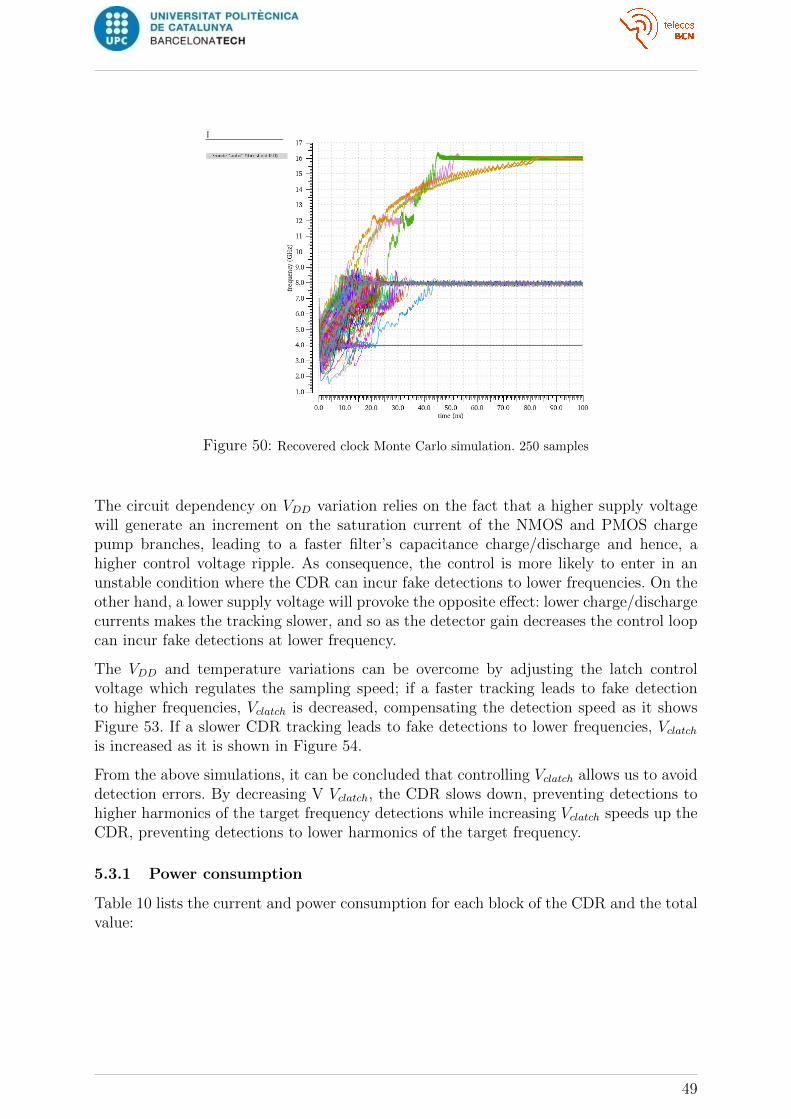
Figure 50: Recovered clock Monte Carlo simulation. 250 samples
The circuit dependency on VDD variation relies on the fact that a higher supply voltagewill generate an increment on the saturation current of the NMOS and PMOS chargepump branches, leading to a faster filter’s capacitance charge/discharge and hence, ahigher control voltage ripple. As consequence, the control is more likely to enter in anunstable condition where the CDR can incur fake detections to lower frequencies. On theother hand, a lower supply voltage will provoke the opposite effect: lower charge/dischargecurrents makes the tracking slower, and so as the detector gain decreases the control loopcan incur fake detections at lower frequency.
The VDD and temperature variations can be overcome by adjusting the latch controlvoltage which regulates the sampling speed; if a faster tracking leads to fake detectionto higher frequencies, Vclatch is decreased, compensating the detection speed as it showsFigure 53. If a slower CDR tracking leads to fake detections to lower frequencies, Vclatchis increased as it is shown in Figure 54.
From the above simulations, it can be concluded that controlling Vclatch allows us to avoiddetection errors. By decreasing V Vclatch, the CDR slows down, preventing detections tohigher harmonics of the target frequency detections while increasing Vclatch speeds up theCDR, preventing detections to lower harmonics of the target frequency.
5.3.1 Power consumption
Table 10 lists the current and power consumption for each block of the CDR and the totalvalue:
49

Figure 51: Steady-state worse and best cases
Block I (mA) P (mW)Phase detector 0.43 0.34Charge pump 0.14 0.11VCO 1.17 0.94TOTAL 1.73 1.38
Table 10: Current and power consumption for each block of the CDR
Figure 52: Settling time worse and best cases
50

Figure 53: Monte Carlo simulation at corner VDD=0.88 V, T=125C where the clock frequency goesbeyond 8 GHz. Vclatch is adjusted from (a) 700 mV to (b) 500 mV
Figure 54: Monte Carlo simulation at corner (VDD=0.72 V T=-40C) where the clock frequency doesnot reach 8 GHz. Vclatch is adjusted from (a) 700 mV to (b) 770 mV
51

6 Conclusions and future development
In this work, we have designed an analog PLL-based clock recovery circuit implementedin a 22 nm FDSOI technology that is able to track an 8 Gbps input data bit-streamwith a settling time of 22 ns and a generated jitter in the recovered clock that reaches amaximum of 0.016 UI (970 fs RMS).
The CDR phase detector is implemented as a linear detector based on CML flip-flopsthat, along with a gain-boosted charge pump, generates a current/error-phase gain of 6.4µA/rad.
The VCO has been designed as a five-stage, current-starved ring oscillator with a singledended to differential output topology that achieves a frequency tuning range from 2.5GHz to 12 GHz, allowing the operation with multi-Gbps systems protocols such as Xilinx-Aurora, CEI-6G and CEI-11G.
The loop filter consists of a passive low pass filter for a 3rd order type II PLL with abandwidth of 150MHz. The simulation results indicates that the filter rejects the inputtransferred jitter down to 9.7 ps RMS (0.16 UI) when an input data distorted with 0.24UIpp jitter is applied. Furthermore, the 150 MHz bandwidth allows a recovered clock jitterbudget of 23.4 ps for a BER = 10−12.
Table 11 summarizes the operation characteristics of the proposed CDR in comparison tothe state of the art designs.
This work [7] [8] [9] [10]Technology 22nm SOI 22nm SOI 65nm 65ns 45nm
Voltage supply 0.8 V 0.8 V 1.2 V 1 V 1 VData rate 8 Gbps 16 Gbps 1-16 Gbps 20 Gbps 25 GbpsFrequency
tuning2.5-12 GHz - 4-8 GHz 18.6-21.6
GHz12.25-13.59GHz
Filterbandwidth
150 MHz - - 170 MHz 6 MHz
Clock RMSJitter
0.016 UI 0.03 UI 0.19 UI 0.018 UI 0.075 UI
Jitter Tolerance(BER=10−12)
- - 0.2 UIpp 0.7 UIpp 0.3 UIpp
Powerconsumption
1.38 mW 80 mW 87 mW 3 mW 4.97 mW
Table 11: Comparison of CDR designs reported in literature and this work
From this design, the following conclusions have been reached:
1. In a 3rd order type II PLL filter, as the separation between the pole (located athigher frequencies) and the zero (located at lower frequencies) increases, the phasemargin, that defines the stability of the closed-loop operation, also increases. Thisimplies a more damped step response and shorter settling time. Therefore, the linear
52

control model intended to work with a 35 phase margin was modified during thesimulations to work with a 55 phase margin, improving the system stability andachieving a faster clock recovery with a settling time of 11.6 ns.
2. The recovered clock RMS jitter generated by the CDR could be attenuated downto 970 fs by decreasing the charge pump output current from 68 µA to 40 µA. Thisadjustment increased marginally the 11.6 ns settling time up to 12.2 ns.
3. The design of the loop filter’s 3-dB cutoff frequency determines the trade-off betweenthe input jitter transfer and input jitter tolerance. Narrow bandwidths will allowhaving a stronger input noise attenuation. However, it slows down the frequencytracking and the stability can be compromised when very noisy inputs make theCDR increase its BER. If the input signal is expected to be a fairly clean signal, anarrow bandwidth will be convenient. On the other hand, wider bandwidths allowthe CDR to have more immunity or tolerance to the noise embedded in the inputsignal, as well as increasing the tracking speed. However, the output clock willpresent more noisy behavior. For the final design, a wide bandwidth (150 MHz)was implemented to achieve a clock jitter budget of 23.4 ps under a BER = 10−12
condition and a settling time of 22 ns, assuming an input signal with 0.024 UIppjitter.
4. The simulated power consumption shows an improvement from the state the artdesign specifications. The circuit dissipates 1.38mW, two times less than the lowestpower consumption specified in the literature.
5. A Monte Carlo simulation of 250 samples has been performed employing 6 statisticalcorners where the VDD and temperature were varying. 4.4% of the simulation failedto recover the clock at the target frequency. Nevertheless, an external control voltagefor the phase detector has been implemented to adjust the current that feeds thelatches of the flip flops to regulate the detection speed and compensate the process,power supply and temperature variations that lead to failed detections to lock inthe right frequency for all simulated cases.
As future development the CDR jitter tolerance will be characterized by implementinga phase-modulated PRBS where a sinusoidal jitter signal with a defined frequency rangemodulates the data. The tolerance will be obtained by the CDR response to the differentjitter frequencies.
The layout of the CDR will be designed. New simulations will be performed includingthe parasitics extracted from the layout and some design parameters will be adjusted ifnecessary to improve the circuit performance.
53

References
[1] E Erra. Study of ASIC Serial Memory Interface Design. Bachelor’s thesis, UPC,Escola Tecnica Superior d’Enginyeria de Telecomunicacio de Barcelona, Sep 2020.
[2] Global Foundries. FD-SOI Technology Innovations Extend Moore’s Law, A GlobalFoundries White Paper, September 2015.
[3] Hanqiao Zhang, Steven Krooswyk, and Jeff Ou. Link Circuits and Architecture. InHigh Speed Digital Design, pages 163–198. Morgan Kaufmann, Boston, 2015.
[4] Lei Xiao, Wei Liu, and Lianxing Yang. Low jitter design for ring oscillator in Serdes.In 2007 7th International Conference on ASIC, pages 307–310, 2007.
[5] D. Mukherjee, J. Bhattacharjee, and J. Laskar. A differentially-tuned CMOS LCVCO for low-voltage full-rate 10 Gb/s CDR circuit. In 2002 IEEE MTT-S Interna-tional Microwave Symposium Digest (Cat. No.02CH37278), volume 2, pages 707–710vol.2, 2002.
[6] J. E. Rogers and J. R. Long. A 10 Gb/s CDR/DEMUX with LC delay line VCO in0.18 /spl mu/m CMOS. In 2002 IEEE International Solid-State Circuits Conference.Digest of Technical Papers (Cat. No.02CH37315), volume 1, pages 254–465 vol.1,2002.
[7] S. Guo, L. Ding, and J. Jin. A 16/32Gb/s NRZ/PAM4 Receiver with Dual-Loop CDRand Threshold Voltage Calibration. In 2019 IEEE 13th International Conference onASIC (ASICON), pages 1–4, 2019.
[8] G. Wu, D. Huang, J. Li, P. Gui, T. Liu, S. Guo, R. Wang, Y. Fan, S. Chakraborty,and M. Morgan. A 1–16 Gb/s All-Digital Clock and Data Recovery With a Wide-band High-Linearity Phase Interpolator. IEEE Transactions on Very Large ScaleIntegration (VLSI) Systems, 24(7):2511–2520, 2016.
[9] L. Kong, Y. Chang, and B. Razavi. An Inductorless 20-Gb/s CDR With High JitterTolerance. IEEE Journal of Solid-State Circuits, 54(10):2857–2866, 2019.
[10] J. W. Jung and B. Razavi. A 25-Gb/s 5-mW CMOS CDR/Deserializer. IEEEJournal of Solid-State Circuits, 48(3):684–697, 2013.
[11] Xilinx. Aurora 8B/10B Protocol Specification, Oct 2014. SP002, v2.3.
[12] Xilinx. Virtex-5 FPGA RocketIO GTX Transceiver CEI-6G Electrical Specification,Oct 2008. RPT113, v1.0.
[13] Xilinx. Virtex-6 FPGA GTH Transceivers CEI-11G-SR, CEI-11G-MR (Low Swing)and CAUI Electrical Interface, Jun 2011. RPT135, v1.0.
[14] Behzad Razavi. Design of CMOS Phase-Locked Loops: From Circuit Level to Archi-tecture Level, page 445. Cambridge University Press, 2020.
[15] S. Goldman. Phase-Locked Loop Engineering Handbook for Integrated Circuits,page 28. Artech, 2007.
54

[16] Y. . Choi and D. . Han. Gain-Boosting Charge Pump for Current Matching inPhase-Locked Loop. IEEE Transactions on Circuits and Systems II: Express Briefs,53(10):1022–1025, 2006.
[17] P. Rajalingam, S. Jayakumar, and S. Routray. Design and Analysis of Low Powerand High Frequency Current Starved Sleep Voltage Controlled Oscillator for PhaseLocked Loop Application. Silicon, pages 1–12, 2020.
[18] Y. Toh and J. A. McNeill. Single-ended to differential converter for multiple-stagesingle-ended ring oscillators. IEEE Journal of Solid-State Circuits, 38(1):141–145,2003.
[19] B. Razavi. Design of Analog CMOS Integrated Circuits, pages 560–562. McGraw-Hillelectrical engineering series. McGraw-Hill, 2001.
[20] S. Long. Lecture notes in Communication Electronics. ECE Department, Universityof California, https://web.ece.ucsb.edu/~long/ece145b/TOPLL.pdf, 2011.
[21] D. Shaeffer. Formulating design criteria for frequency generation for wireless appli-cations. In Sesion F1, Girafe Design Forum. ISSCC, 2005.
[22] S. Goldman. Phase-Locked Loop Engineering Handbook for Integrated Circuits, page334. Artech, 2007.
[23] Hanane Gholamnataj and Habib Adrang. Comprehensive Study of the Third-orderCharge Pump PLL Dynamic Behavior. Majlesi Journal of Telecommunication De-vices, 3, 2014.
[24] National Semiconductor. An Analysis and Performance Evaluation of a Passive FilterDesign Technique for Charge Pump PLL’s, Aplication Note 1001, July 2011.
[25] Ken Kundert. Modeling Jitter in PLL-based Frequency Synthesizers, The Design-ers Guide Community. https://designers-guide.org/analysis/PLLjitter.pdf,March 2012. (Accessed on 02/15/2021).
[26] R. Carter, J. Mazurier, and L. Pirro. 22nm FDSOI technology for emerging mo-bile, Internet-of-Things, and RF applications. In 2016 IEEE International ElectronDevices Meeting (IEDM), pages 2.2.1–2.2.4, 2016.
[27] G. Scotti, D. Bellizia, A. Trifiletti, and G. Palumbo. Design of Low-Voltage High-Speed CML D-Latches in Nanometer CMOS Technologies. IEEE Transactions onVery Large Scale Integration (VLSI) Systems, 25(12):3509–3520, 2017.
[28] G. Scotti, A. Trifiletti, and G. Palumbo. A Novel 0.5 V MCML D-Flip-Flop TopologyExploiting Forward Body Bias Threshold Lowering. IEEE Transactions on Circuitsand Systems II: Express Briefs, 67(3):560–564, 2020.
[29] Roland E. Best. Phase-locked loops: design, simulation, and applications, page156–163. McGraw-Hill, 2007.
[30] Mohammad Azadeh. Fiber Optics Engineering, page 256. Springer US, 2009.
55

[31] Behzad Razavi. Design of CMOS Phase-Locked Loops: From Circuit Level to Archi-tecture Level, pages 449–450. Cambridge University Press, 2020.
56

List of terms and abbreviations
CDR: Clock and data recovery.
PLL: Phase locked loop.
VCO: Voltage controlled oscillator
ROSC: Ring oscillator
CSROSC: Current-starved ring oscillator.
RJ: Random jitter.
UI: Unit interval.
PRBS: Pseudo random bit sequence.
BER: Bit eror rate.
FDSOI: Fully-depleted silicon on insulator
CML: Current mode logic.
BW: Bandwidth.
RMS: Root mean square.
SERDES: Serializer-Deserializer
NRZ: Non return to zero.
CP: Charge pump.
PD: Phase detector.
FPGA: Field programmable gate array.
DDR: Double Data Rate.
RAM: Random access memory
ASIC: Application-specific integrated. circuit
ADE: Analog design environment.
57