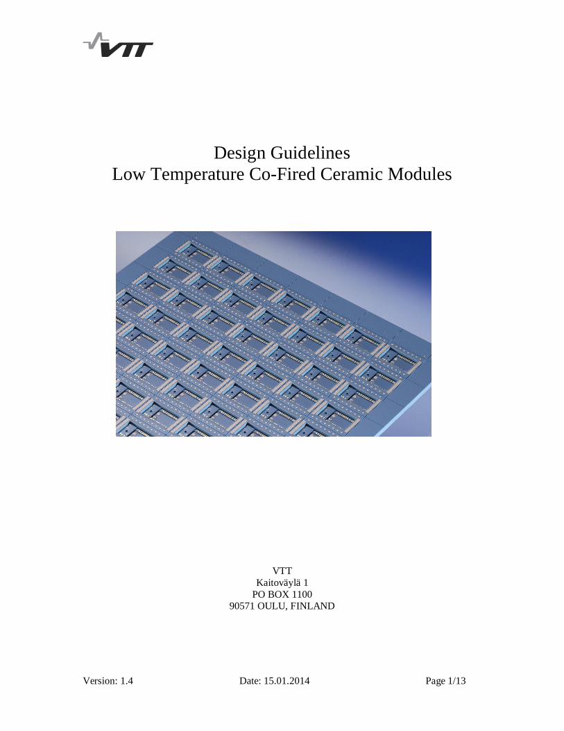
Design Guidelines Low Temperature Co-Fired Ceramic … Temperature Co-Fired Ceramic Modules VTT...
13
Version: 1.4 Date: 15.01.2014 Page 1/13 Design Guidelines Low Temperature Co-Fired Ceramic Modules VTT Kaitoväylä 1 PO BOX 1100 90571 OULU, FINLAND
Transcript of Design Guidelines Low Temperature Co-Fired Ceramic … Temperature Co-Fired Ceramic Modules VTT...
Version: 1.4 Date: 15.01.2014 Page 1/13
Design GuidelinesLow Temperature Co-Fired Ceramic Modules
VTTKaitoväylä 1
PO BOX 110090571 OULU, FINLAND
Version: 1.4 Date: 15.01.2014 Page 2/13
1. INTRODUCTION
VTT Technical Research Centre of Finland offers development and prototyping of LowTemperature Co-Fired Ceramic (LTCC) Modules for different application areas, such astelecommunication, photonics and instrumentation. LTCC substrates are processed with highquality equipment, which allows for small manufacturing tolerances and short cycle time.Component assembly services for the prototype series include SMD components, bare die wirebonded and flip chipped, BGA, hermetic sealing etc. Design services are also available.
This document provides our customers the basic guidelines for the physical design of highvolume and low cost LTCC circuits, using Du Pont 951 material system. All dimensional valuesgiven are fired values for the completed part. The design criteria of this document is in goodunderstanding with the design rules given by commercial LTCC vendors, enabling smoothtransfer to production. Smaller line width and spacing is possible for low volume products and fordevelopment purposes but the design shall be discussed with VTT.
Design guidelines for mm- wave applications using Ferro A6M material system are given uponrequest.
The layout design is made to the fired dimensions, one up basis. Metric system is used. Multi uppanelization and scaling is done at VTT.
2. MATERIAL SYSTEM
Material data for the Du Pont 951 tape dielectric with different thickness is given in Table 1
Table 1. Du Pont 951 tape material data

Version: 1.4 Date: 15.01.2014 Page 3/13
PROPERTY VALUE
Thickness 1) 951-PX 951-P2 951-PT 951-C2
205 m130 m 90 m 40 m
Dielectric constant 7.8 (3 GHz)
Dissipation factor 0.6% (3 GHz)
Insulation resistance >1012 (100VDC)
Breakdown voltage >1000V/ 25 m
Colour blue
Thermal conductivity 3.3 W/mK
Thermal expansion 5.8 ppm/K (25...300 oC)
Fired density 3.1 g/cm3
Surface roughness < 0.34 m
1) Fired thickness based on incoming inspectionList of commonly used conductors, co-fired and post fired, are given in tables 2 and 3.
Table 2. Co-fired conductorsUSAGE DU PONT TYPE
Via Fill 6141 Ag
Via Fill 5738 Au
Transition Via Fill 6138 AgPd
Buried / Surface Conductor 6142D Ag
Buried / Surface Conductor, bondable 5742 Au
Surface Conductor, solderable 6146 AgPd
Surface Conductor, solderable 6336 AgPt
Table 3. Post fired conductorsUSAGE DU PONT TYPE
Brazable conductor 5081 / 5082 AgPdPt
Brazable conductor 5062D / 5063D Au
Version: 1.4 Date: 15.01.2014 Page 4/13
3. SUBSTRATE SIZE AND TOLERANCES
3.1 substrate size and partitioning
Three substrate sizes are available (effective area): 114mm x 114mm, 114mm x 50mm and 50mmx 50mm. With other tape systems besides Du Pont 951 please consult VTT for substrate sizes.
Parts can be supplied individually diced or in array format readily scored using a hot blade at thelaminated stage to be snapped later.
Finished part outer dimension tolerance is generally +/- 0.7 % of part size but not less than +/-100 m for green cut parts.
The shrinkage tolerance of circuit features in x and y direction is typically less than +/- 0.1 %(production +/- 0.2% typically).
3.2 Part thickness
The minimum recommended substrate thickness is 500 m. Smaller thickness is possible for asmall part size. Table 1 in section 2 gives the average fired layer thickness for different tapeversions.
Layer thickness tolerance is +/- 5 % , but typically < +/- 2% within manufacturing lot.
Version: 1.4 Date: 15.01.2014 Page 5/13
4. VIAS
4.1 Via materials
Pure Ag vias are used with Ag bearing conductors. Au vias are used with Au conductors.
Transition AgPd vias are used to contact surface Au conductor to a buried Ag metallization.Transition vias shall not be stacked.
4.2 Via sizes
Via sizes are 80 m, 100 m, 150 m and 200 m, as punched to the unfired tape. The viasshrink about 10% when co-fired. Via diameter is recommended to be close to the tape thickness.It is recommended to use one via diameter on any tape layer. Two or three via diameters on anytape layer is allowed, however.
4.3 Via catch pads
A line connection to a via less than 200 m in diameter shall have a round catch pad which is 50m larger than the via diameter. For prototyping purposes, the catch pads for stacked vias larger
than 100 m can be left out.
Catch pad diameter of 380 m shall be used for post- fired surface conductors.
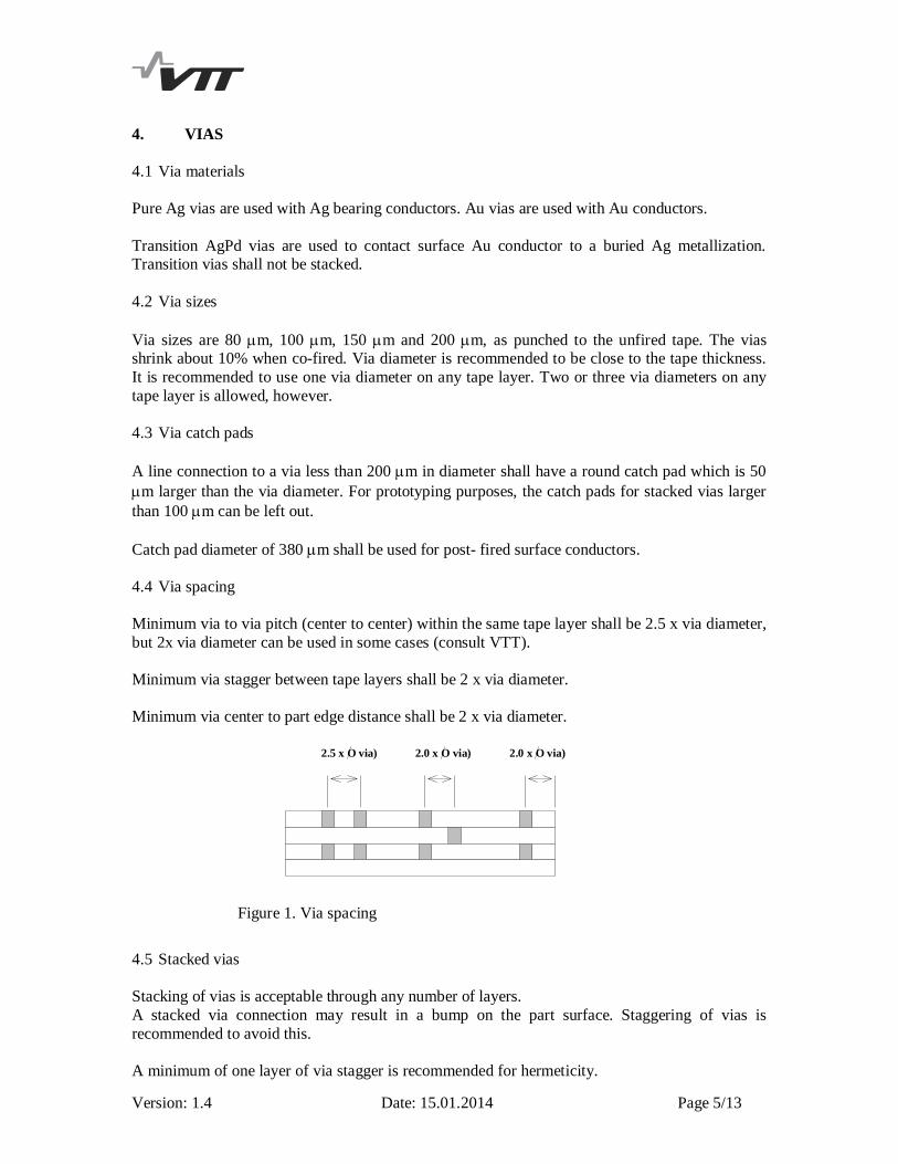
4.4 Via spacing
Minimum via to via pitch (center to center) within the same tape layer shall be 2.5 x via diameter,but 2x via diameter can be used in some cases (consult VTT).
Minimum via stagger between tape layers shall be 2 x via diameter.
Minimum via center to part edge distance shall be 2 x via diameter.
Figure 1. Via spacing
4.5 Stacked vias
Stacking of vias is acceptable through any number of layers.A stacked via connection may result in a bump on the part surface. Staggering of vias isrecommended to avoid this.
A minimum of one layer of via stagger is recommended for hermeticity.
2.5 x O via) 2.0 x O via) 2.0 x O via)

Version: 1.4 Date: 15.01.2014 Page 6/13
4.6 Thermal vias
Recommended thermal via diameter is 200 m for tape materials 951-P2 and 951-PX and 150 mfor 951-PT.
The minimum via pitch (center to center) in a thermal via array shall be 2 x via diameter.
The maximum thermal via array size is 6.5 mm length and width.
The minimum thermal via array to part edge clearance shall be 2 mm.
5. CONDUCTORS
Figure 2. Conductors
5.1 Line width and spacing
Following line width and space guidelines are for high volume processing, enabling highmanufacturing yield. Smaller line width and spacing is possible for low volume products and fordevelopment purposes after consulting VTT.
The minimum conductor line width shall be 100 m (A). Maximum line width is 1.5 mm withunlimited length. The use of 90o lines is recommended for the optimum line width control, but 45o
lines are allowed.
The minimum conductor spacing shall be 150 m (B).
The minimum conductor line spacing to a via catch pad shall be 125 m (C).
The minimum conductor line clearance to the substrate edge shall be 250 m (D). Lead frame padclearance to the substrate edge shall be 125 m.
The minimum SMD pad spacing to a via catch pad or a conductor line shall be 200 m (E).
The minimum SMD pad spacing to substrate edge shall be 500 m (F).
ABC
D
Square End
Via Cover Pad
Substrate Edge
E
F
Version: 1.4 Date: 15.01.2014 Page 7/13
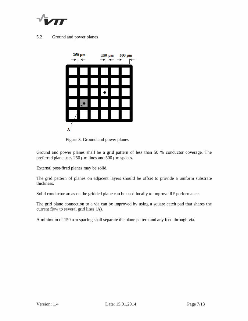
5.2 Ground and power planes
Figure 3. Ground and power planes
Ground and power planes shall be a grid pattern of less than 50 % conductor coverage. Thepreferred plane uses 250 m lines and 500 m spaces.
External post-fired planes may be solid.
The grid pattern of planes on adjacent layers should be offset to provide a uniform substratethickness.
Solid conductor areas on the gridded plane can be used locally to improve RF performance.
The grid plane connection to a via can be improved by using a square catch pad that shares thecurrent flow to several grid lines (A).
A minimum of 150 m spacing shall separate the plane pattern and any feed through via.
Version: 1.4 Date: 15.01.2014 Page 8/13
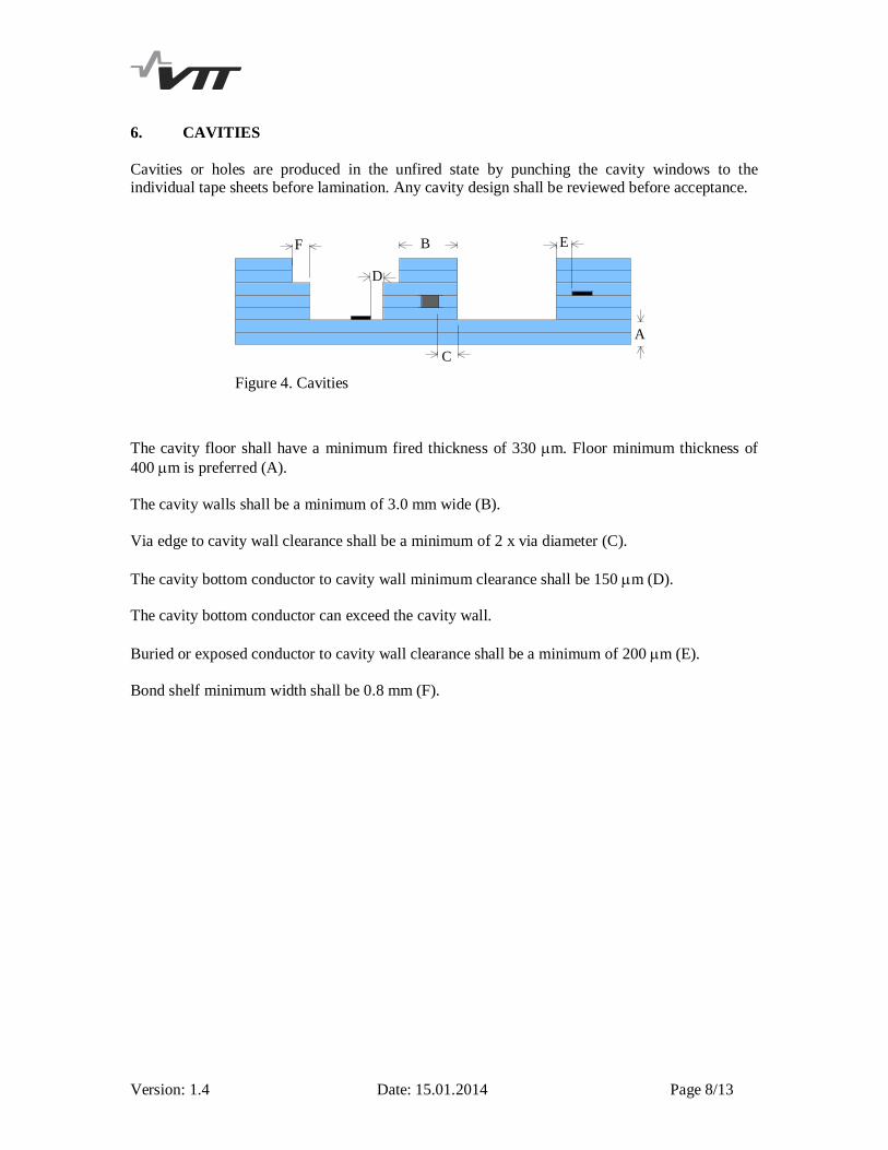
6. CAVITIES
Cavities or holes are produced in the unfired state by punching the cavity windows to theindividual tape sheets before lamination. Any cavity design shall be reviewed before acceptance.
A
B E
D
C
F
Figure 4. Cavities
The cavity floor shall have a minimum fired thickness of 330 m. Floor minimum thickness of400 m is preferred (A).
The cavity walls shall be a minimum of 3.0 mm wide (B).
Via edge to cavity wall clearance shall be a minimum of 2 x via diameter (C).
The cavity bottom conductor to cavity wall minimum clearance shall be 150 m (D).
The cavity bottom conductor can exceed the cavity wall.
Buried or exposed conductor to cavity wall clearance shall be a minimum of 200 m (E).
Bond shelf minimum width shall be 0.8 mm (F).

Version: 1.4 Date: 15.01.2014 Page 9/13
7. I / O STYLES
7.1 Clip leads
Clip lead frames with a lead pitch of 2.54 mm and 1.27 mm are normally used. Different leadconfigurations are available from clip lead manufacturers for surface mount and through holemount applications.
Solder pad for the clip lead is printed on the substrate top and bottom side.
min
0.5
2.54
Pitch 2.54Pad Size 1.8mm x 1.5mm
0.125
min
0.5
0.125
1.27
Pitch 1.27Pad Size 1.5mm x 0.9mm
Figure 5. Lead frame pads
7.2 BGA
Ball grid array can be made on the substrate top or bottom surface using Pb90/Sn10 solder ballsattached with lead free solder.
Figure 6. BGA solder pads with dielectric solder stop
Version: 1.4 Date: 15.01.2014 Page 10/13
BGA pad sizes and pad pitch depend on solder ball size. Following table gives the pad design fordifferent solder ball sizes.
Ball diameter (mm) Pad size ( A )
(mm)
Dielectric I.D. ( B )
(mm)
Pad pitch min. ( C )
(mm)
0.85 1.02 0.82 1.5
0.70 0.87 0.67 1.27
0.40 0.57 0.37 1.0
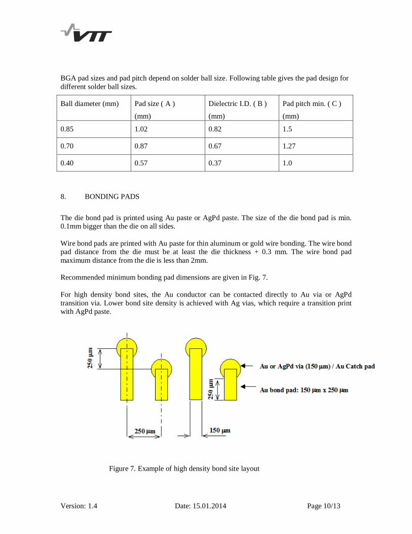
8. BONDING PADS
The die bond pad is printed using Au paste or AgPd paste. The size of the die bond pad is min.0.1mm bigger than the die on all sides.
Wire bond pads are printed with Au paste for thin aluminum or gold wire bonding. The wire bondpad distance from the die must be at least the die thickness + 0.3 mm. The wire bond padmaximum distance from the die is less than 2mm.
Recommended minimum bonding pad dimensions are given in Fig. 7.
For high density bond sites, the Au conductor can be contacted directly to Au via or AgPdtransition via. Lower bond site density is achieved with Ag vias, which require a transition printwith AgPd paste.
Figure 7. Example of high density bond site layout
Version: 1.4 Date: 15.01.2014 Page 11/13
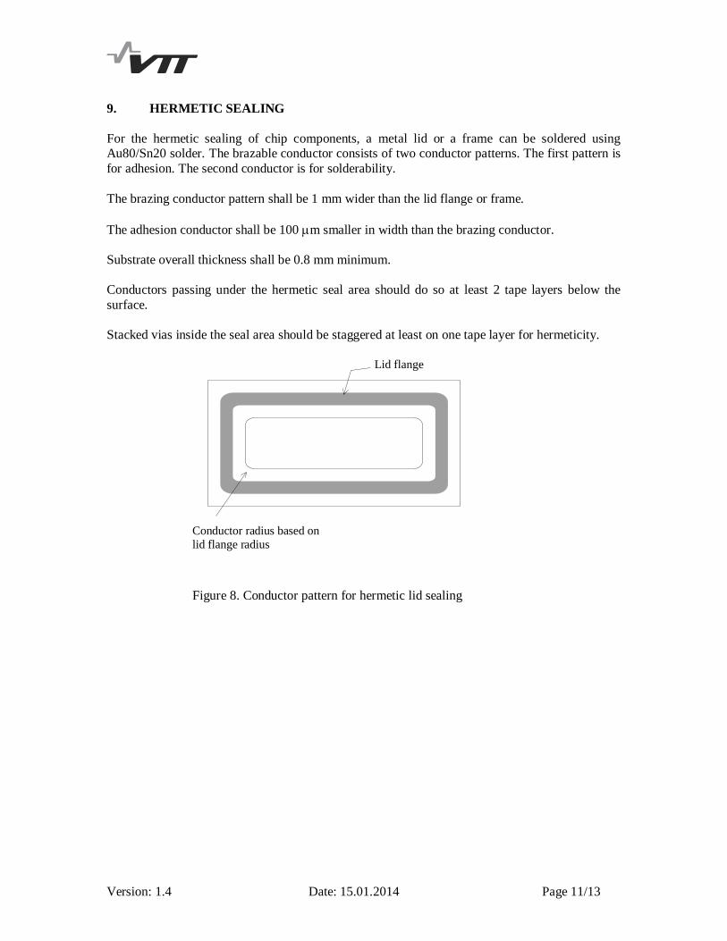
9. HERMETIC SEALING
For the hermetic sealing of chip components, a metal lid or a frame can be soldered usingAu80/Sn20 solder. The brazable conductor consists of two conductor patterns. The first pattern isfor adhesion. The second conductor is for solderability.
The brazing conductor pattern shall be 1 mm wider than the lid flange or frame.
The adhesion conductor shall be 100 m smaller in width than the brazing conductor.
Substrate overall thickness shall be 0.8 mm minimum.
Conductors passing under the hermetic seal area should do so at least 2 tape layers below thesurface.
Stacked vias inside the seal area should be staggered at least on one tape layer for hermeticity.
Conductor radius based onlid flange radius
Lid flange
Figure 8. Conductor pattern for hermetic lid sealing

Version: 1.4 Date: 15.01.2014 Page 12/13
10. DESIGN TRANSFER
10.1 Layout considerations
The design is made in one up configuration.
All design layers shall include a substrate outline (line width 100µm).
All designs use a common origin at the center of the part.
10.2 Layer naming scheme
Layers shall be identified using a naming scheme shown in fig. 10. Layers are numbered frombottom to top. Character b after layer number indicates bottom of tape.
TL8 / VIA8
TOP OF SUBSTRATE
BOTTOM OF SUBSTRATE
L8aa
TL7 / VIA7
L2
L1
TL3 / VIA3
TL2 / VIA2
TL1 / VIA1
L3
L6
L7
L1bL1ba
L1bb
L8L8a
L8ab
. . .TL6 / VIA6
Figure 9. Layer naming scheme
Version: 1.4 Date: 15.01.2014 Page 13/13
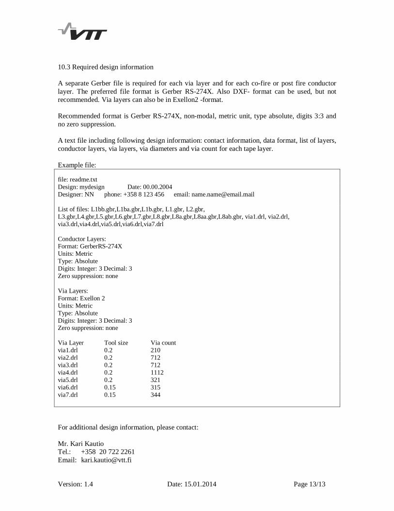
10.3 Required design information
A separate Gerber file is required for each via layer and for each co-fire or post fire conductorlayer. The preferred file format is Gerber RS-274X. Also DXF- format can be used, but notrecommended. Via layers can also be in Exellon2 -format.
Recommended format is Gerber RS-274X, non-modal, metric unit, type absolute, digits 3:3 andno zero suppression.
A text file including following design information: contact information, data format, list of layers,conductor layers, via layers, via diameters and via count for each tape layer.
Example file:
file: readme.txtDesign: mydesign Date: 00.00.2004Designer: NN phone: +358 8 123 456 email: [email protected]
List of files: L1bb.gbr,L1ba.gbr,L1b.gbr, L1.gbr, L2.gbr,L3.gbr,L4.gbr,L5.gbr,L6.gbr,L7.gbr,L8.gbr,L8a.gbr,L8aa.gbr,L8ab.gbr, via1.drl, via2.drl,via3.drl,via4.drl,via5.drl,via6.drl,via7.drl
Conductor Layers:Format: GerberRS-274XUnits: MetricType: AbsoluteDigits: Integer: 3 Decimal: 3Zero suppression: none
Via Layers:Format: Exellon 2Units: MetricType: AbsoluteDigits: Integer: 3 Decimal: 3Zero suppression: none
Via Layer Tool size Via countvia1.drl 0.2 210via2.drl 0.2 712via3.drl 0.2 712via4.drl 0.2 1112via5.drl 0.2 321via6.drl 0.15 315via7.drl 0.15 344
For additional design information, please contact:
Mr. Kari KautioTel.: +358 20 722 2261Email: [email protected]