Design flow approach from inductors to antenna at PCB level
89
San Jose State University San Jose State University SJSU ScholarWorks SJSU ScholarWorks Master's Theses Master's Theses and Graduate Research 2008 Design flow approach from inductors to antenna at PCB level Design flow approach from inductors to antenna at PCB level Joseph C. Chung San Jose State University Follow this and additional works at: https://scholarworks.sjsu.edu/etd_theses Recommended Citation Recommended Citation Chung, Joseph C., "Design flow approach from inductors to antenna at PCB level" (2008). Master's Theses. 3521. DOI: https://doi.org/10.31979/etd.gx7n-dygs https://scholarworks.sjsu.edu/etd_theses/3521 This Thesis is brought to you for free and open access by the Master's Theses and Graduate Research at SJSU ScholarWorks. It has been accepted for inclusion in Master's Theses by an authorized administrator of SJSU ScholarWorks. For more information, please contact [email protected].
Transcript of Design flow approach from inductors to antenna at PCB level
San Jose State University San Jose State University
SJSU ScholarWorks SJSU ScholarWorks
Master's Theses Master's Theses and Graduate Research
2008
Design flow approach from inductors to antenna at PCB level Design flow approach from inductors to antenna at PCB level
Joseph C. Chung San Jose State University
Follow this and additional works at: https://scholarworks.sjsu.edu/etd_theses
Recommended Citation Recommended Citation Chung, Joseph C., "Design flow approach from inductors to antenna at PCB level" (2008). Master's Theses. 3521. DOI: https://doi.org/10.31979/etd.gx7n-dygs https://scholarworks.sjsu.edu/etd_theses/3521
This Thesis is brought to you for free and open access by the Master's Theses and Graduate Research at SJSU ScholarWorks. It has been accepted for inclusion in Master's Theses by an authorized administrator of SJSU ScholarWorks. For more information, please contact [email protected].
DESIGN FLOW APPROACH FROM INDUCTORS TO ANTENNA AT PCB
LEVEL
A Thesis
Presented to
The Faculty of the Department of Electrical Engineering
San Jose State University
In Partial Fulfillment
of the Requirements for the Degree
Master of Science
by
Joseph C. Chung
May 2008
UMI Number: 1458123
INFORMATION TO USERS
The quality of this reproduction is dependent upon the quality of the copy
submitted. Broken or indistinct print, colored or poor quality illustrations and
photographs, print bleed-through, substandard margins, and improper
alignment can adversely affect reproduction.
In the unlikely event that the author did not send a complete manuscript
and there are missing pages, these will be noted. Also, if unauthorized
copyright material had to be removed, a note will indicate the deletion.
®
UMI UMI Microform 1458123
Copyright 2008 by ProQuest LLC.
All rights reserved. This microform edition is protected against
unauthorized copying under Title 17, United States Code.
ProQuest LLC 789 E. Eisenhower Parkway
PO Box 1346 Ann Arbor, Ml 48106-1346

©2008
Joseph C. Chung
ALL RIGHTS RESERVED
APPROVED FOR THE DEPARTMENT OF ELECTRICAL ENGINEERING
Advisor -7 4 tf/'/j
J&Z&U#4£ fir// Dr. Sotoudeh Hamedi-Hagh
Co-Advisor „••• < W ^ ^ l c / -^<-t^^%
f /
Y Dr. David Parent
Co-Advisor SA&^&^-GA
Dr. Masoud Mostafavi
APPROVED FOR THE UNIVERSITY
It^f&rx^- Off03-/01

ABSTRACT
DESIGN FLOW APPROACH FROM INDUCTORS TO ANTENNA AT PCB
LEVEL
by Joseph C. Chung
Integrated circuits, ICs, and printed circuit boards, PCBs, need to be designed
optimally to complement each other for system level functionality. This is critical in
radio frequencies where inductors and antennas are essential to the system. For
inductor design, PCB is better over silicon as it delivers higher inductance and quality
factor for given cost/area. PCB also provides the ability to design high gain antennas.
This thesis proposes a design flow from inductors to antennas for students in system
design. The flow includes theory, design, simulations as well as fabrication and
measurements. The goal is to characterize a PCB substrate through two inductors to
optimize simulators for a GPS LI antenna design. For intermediate frequency
applications, the larger inductor at 200MHz has measured inductance of 95nH,
resistance of 2.9Q, and quality factor of 51. The antenna has a measured bandwidth
of 250MHz and a return loss of |-36|dB at 1.5754GHz.

ACKNOWLEDGEMENT
I would like to thank my M.S.E.E. thesis advisor, Dr. Sotoudeh Hamedi-Hagh,
for his exceptional guidance. Also, I am grateful for his RFIC lab at San Jose State
University where the measurements for this thesis were made possible.
I would like to thank Dr. G.A. Rezvani from RFMD for his invaluable advice
on calibration and measurement techniques.
Also, I would also like to thank Sonnet Software Inc. and Agilent for their
generosity in allowing the use of their tools.
In addition, I would like to thank my co-advisors, Dr. David Parent and Dr.
Masoud Mostafavi for their support.
Last but not least, I would like to thank my mother, Grace, brother, Raymond,
and girlfriend of eight years, Julie, for their patience and their understanding of the
importance of my work in the completion of this thesis.
v
TABLE OF CONTENTS
1 INTRODUCTION 1 1.1 Inductor Background 1 1.2 Antenna Background 4
1.2.1 Antenna Applications - GPS Background 6 1.3 Summary and Thesis Outline 7
2 THEORY, ANALYSIS, AND DESIGN 9 2.1 Inductor 9
2.1.1 Inductance 9 2.1.2 Resistance 16 2.1.3 Quality Factor 19
2.2 Antenna 20 2.2.1 Proposed Geometry 21 2.2.2 Radiation Pattern 22 2.2.3 Directivity and Gain 24 2.2.4 Polarization 25 2.2.5 Impedance Bandwidth and Q-factor 29
2.3 Chapter Summary 33 3 SIMULATIONS 34
3.1 Inductors 34 3.1.1 Inductance 40 3.1.2 Resistance 41 3.1.3 Quality Factor 43
3.2 Transition from Inductor to Antenna 44 3.3 Antenna 46
3.3.1 Radiation Pattern 46 3.3.2 Directivity and Gain 47 3.3.3 Polarization 49 3.3.4 Impedance Bandwidth 50
3.4 Chapter Summary 51 4 MEASUREMENTS 52
4.1 Measurement Conditions 52 4.2 Calibration and De-embedding 53
4.2.1 VNA and Calibration 53 4.2.2 PCB Trace De-embedding 55
4.3 Inductors 59 4.3.1 Inductance 62 4.3.2 Resistance 64 4.3.3 Quality Factor 66 4.3.4 Results 67
4.4 Transition from Inductor to Antenna 68 4.5 Antenna 68
4.5.1 Impedance Matching 69
VI

4.5.2 Results 70 4.6 Chapter Summary 71
5 CONCLUSION 72 References 74
vii
LIST OF TABLES
Table 1-1 Inductor Tradeoffs - PCB vs. Silicon 3 Table 1-2 Antenna Tradeoffs - PCB vs. Silicon 5 Table 3-1 ADS Antenna Dialog 48 Table 4-1 Twelve Error Terms 54 Table 4-2 Inductor 'A' Parameter Summary 67 Table 4-3 Inductor 'B' Parameter Summary 68 Table 4-4 Summary of Impedance Matching and Bandwidth 70
viii
LIST OF FIGURES
Fig. 1-1 Typical Toroid 1 Fig. 1-2 Typical Rod 2 Fig. 1-3 Model for Inductor on Silicon 3 Fig. 1-4 Model for Inductor on FR4 PCB 3 Fig. 1-5 Typical Yagi Antenna 4 Fig. 1-6 Typical Whip Antenna 5 Fig. 2-1 Visual of Current Flow Direction for Square Inductor 12 Fig. 2-2 Dimensions of Proposed Square Inductor 'A' 15 Fig. 2-3 Dimensions of Proposed Square Inductor 'B' 16 Fig. 2-4 Proposed Geometry of Antenna 22 Fig. 2-5 Polar References 23 Fig. 2-6 Visual of Linear Polarization 26 Fig. 2-7 Visual of (a) Right Hand Circular Polarization and (b) Left Hand Circular Polarization 27 Fig. 2-8 Various Circular Polarization Patch Methods 28 Fig. 3-1 ADS Layout of Inductor 'A' 34 Fig. 3-2 ADS Layout of Inductor 'B' 35 Fig. 3-3 Sonnet Layout of Inductor 'A' 36 Fig. 3-4 Sonnet Layout of Inductor 'B ' 36 Fig. 3-5 Simulated Sn Parameters of (a) Inductor 'A' and (b) Inductor 'B ' 37 Fig. 3-6 Simulated S21 Parameters of (a) Inductor 'A' and (b) Inductor 'B' 38 Fig. 3-7 Simulated S12 Parameters of (a) Inductor 'A' and (b) Inductor 'B' 39 Fig. 3-8 Simulated S22 Parameters of (a) Inductor 'A' and (b) Inductor 'B ' 39 Fig. 3-9 Simulated Inductance of Inductor 'A' 40 Fig. 3-10 Simulated Inductance of Inductor 'B' 41 Fig. 3-11 Simulated Resistance of Inductor 'A' 42 Fig. 3-12 Simulated Resistance of Inductor 'B' 42 Fig. 3-13 Simulated Resistance of Inductor 'A' 43 Fig. 3-14 Simulated Resistance of Inductor 'B' 44 Fig. 3-15 Flow Chart of Design Process 45 Fig. 3-16 E-field Radiation Pattern 47 Fig. 3-17 Sonnet Theta vs. Gain 48 Fig. 3-18 Right Hand Circular Polarization Pattern 49 Fig. 3-19 Simulated Sn of Antenna Design 50 Fig. 4-1 Transfer Data from Network Analyzer to Matlab 52 Fig. 4-2 Fabricated Inductors with De-embedding Circuits 56 Fig. 4-3 Example of the Effects of Trace De-embedding (Using Open-Shorts) 57 Fig. 4-4 Layout for Fabrication for Inductor 'A' 59 Fig. 4-5 Layout for Fabrication for Inductor 'B' 59 Fig. 4-6 Measured Sn Parameters of (a) Inductor 'A' and (b) Inductor 'B' 60 Fig. 4-7 Measured S12 Parameters of (a) Inductor 'A' and (b) Inductor 'B' 61 Fig. 4-8 Measured S21 Parameters of (a) Inductor 'A' and (b) Inductor 'B ' 61
IX
Fig. 4-9 Measured S22 Parameters of (a) Inductor 'A' and (b) Inductor 'B' 62 Fig. 4-10 Measured Inductance of Inductor 'A' Relative to Simulations 63 Fig. 4-11 Measured Inductance of Inductor 'B ' Relative to Simulations 64 Fig. 4-12 Measured Resistance of Inductor 'A' Relative to Simulations 65 Fig. 4-13 Measured Resistance of Inductor 'B ' Relative to Simulations 65 Fig. 4-14 Measured Q-factor of Inductor 'A' Relative to Simulations 66 Fig. 4-15 Measured Q-factor of Inductor 'B' Relative to Simulations 67 Fig. 4-16 Front and Back Pictures of L-ground Plane with Lowercase-h Configuration and Cornered Patch 69 Fig. 4-17 Measured Sn Parameter Relative to Simulations 70
x
1 INTRODUCTION
At the printed circuit board (PCB) level, components such as inductors and
antennas are created from similar traces, yet their application purposes vary
drastically. Inductors are passive components which optimally retains as much
energy within the traces as possible. Antennas on the other hand, optimally radiate as
much energy as possible. The inductor design flow will lead into the design of an
antenna for global positioning system (GPS) applications. The general background as
well as information specific to PCB vs. silicon will be discussed, followed by the
thesis outline.
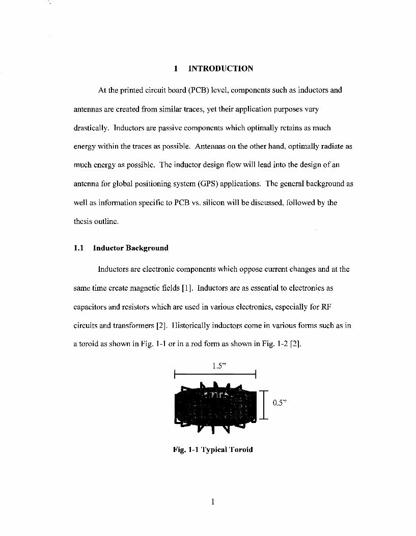
1.1 Inductor Background
Inductors are electronic components which oppose current changes and at the
same time create magnetic fields [1]. Inductors are as essential to electronics as
capacitors and resistors which are used in various electronics, especially for RF
circuits and transformers [2]. Historically inductors come in various forms such as in
a toroid as shown in Fig. 1-1 or in a rod form as shown in Fig. 1-2 [2].
1.5"
Fig. 1-1 Typical Toroid
1
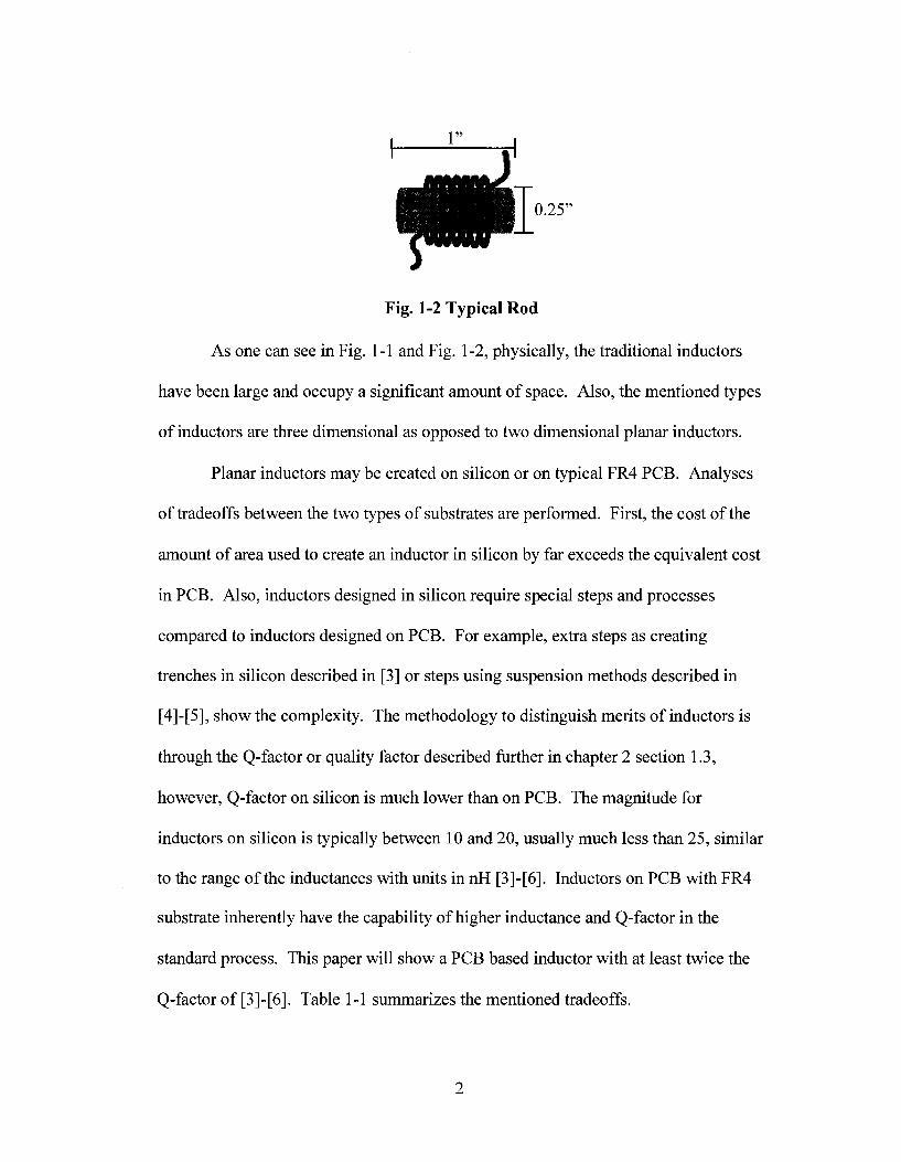
1"
H ^ H H | 0.25"
Fig. 1-2 Typical Rod
As one can see in Fig. 1-1 and Fig. 1-2, physically, the traditional inductors
have been large and occupy a significant amount of space. Also, the mentioned types
of inductors are three dimensional as opposed to two dimensional planar inductors.
Planar inductors may be created on silicon or on typical FR4 PCB. Analyses
of tradeoffs between the two types of substrates are performed. First, the cost of the
amount of area used to create an inductor in silicon by far exceeds the equivalent cost
in PCB. Also, inductors designed in silicon require special steps and processes
compared to inductors designed on PCB. For example, extra steps as creating
trenches in silicon described in [3] or steps using suspension methods described in
[4]-[5], show the complexity. The methodology to distinguish merits of inductors is
through the Q-factor or quality factor described further in chapter 2 section 1.3,
however, Q-factor on silicon is much lower than on PCB. The magnitude for
inductors on silicon is typically between 10 and 20, usually much less than 25, similar
to the range of the inductances with units in nH [3]-[6]. Inductors on PCB with FR4
substrate inherently have the capability of higher inductance and Q-factor in the
standard process. This paper will show a PCB based inductor with at least twice the
Q-factor of [3]-[6]. Table 1-1 summarizes the mentioned tradeoffs.
2
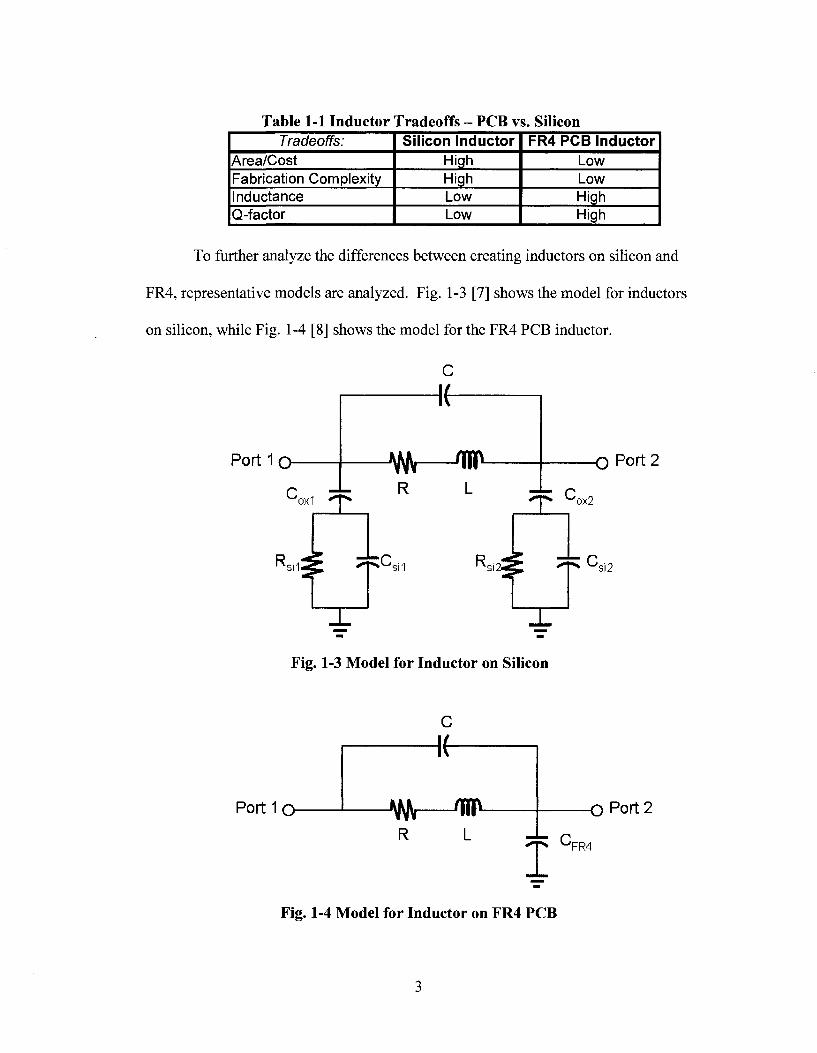
Table 1-1 Inductor Tradeoffs - PCB vs. Silicon Tradeoffs:
Area/Cost Fabrication Complexity Inductance Q-factor
Silicon Inductor High High Low Low
FR4 PCB Inductor Low Low High High
To further analyze the differences between creating inductors on silicon and
FR4, representative models are analyzed. Fig. 1-3 [7] shows the model for inductors
on silicon, while Fig. 1-4 [8] shows the model for the FR4 PCB inductor.
Port 1 Q O Port 2
Fig. 1-3 Model for Inductor on Silicon
Port 1 Q O Port 2
Fig. 1-4 Model for Inductor on FR4 PCB
3
The silicon inductor model shows the inherent inductance, L, and the inherent
series resistance, R. The parasitic capacitance from the oxide between the metal and
silicon is denoted as Cox- Within the silicon, CSj and RSi are parasitic capacitance and
resistance modeled in parallel to each other due to the substrate characteristics,
affecting the Q-factor [9]. Both Fig. 1-3 and Fig. 1-4 show a coupling capacitor C
between the two ports. Fig. 1-4 shows the actual inductance, L, and the series
resistance, R, however, with only a single source of substrate parasitic, CFR4. In
comparing Fig. 1-3 and Fig. 1-4, it is evident that less parastics are in PCB compared
to silicon.
In analyzing the tradeoffs, the inductors are to be designed on FR4. The
applications for the inductors would be for intermediate frequency purposes, which
complements other necessary RF components such as the antenna for system level
applications.
1.2 Antenna Background
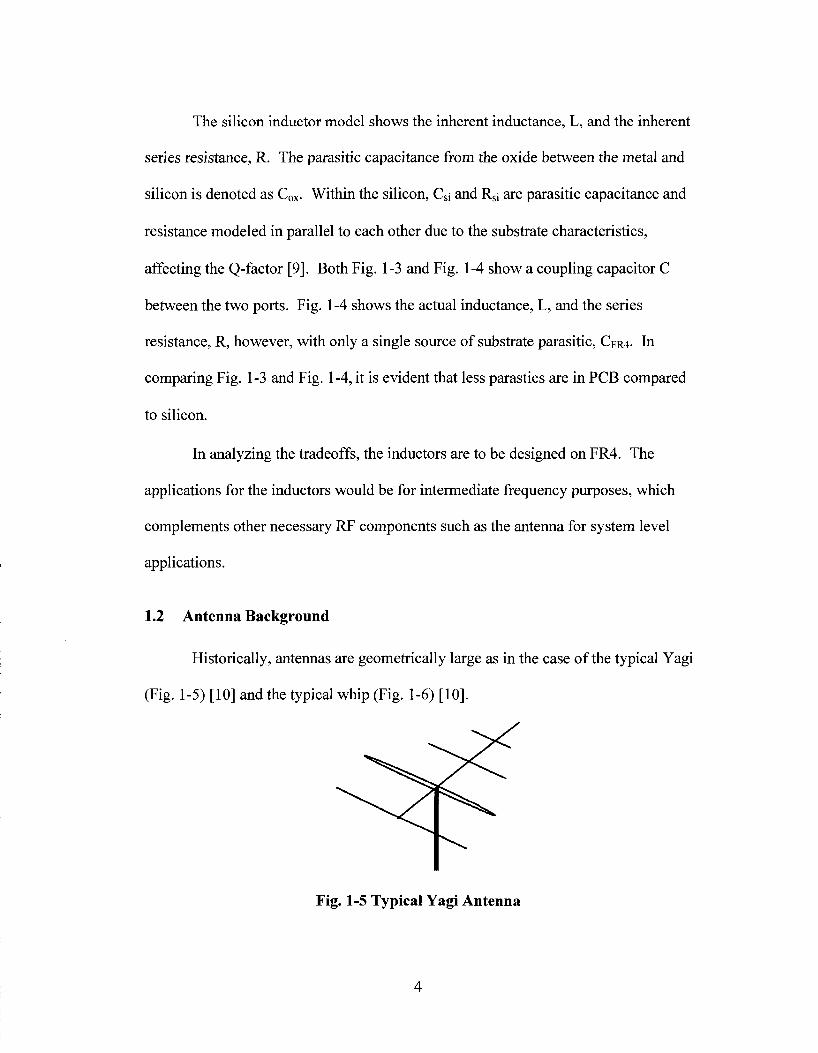
Historically, antennas are geometrically large as in the case of the typical Yagi
(Fig. 1-5) [10] and the typical whip (Fig. 1-6) [10].
Fig. 1-5 Typical Yagi Antenna
4
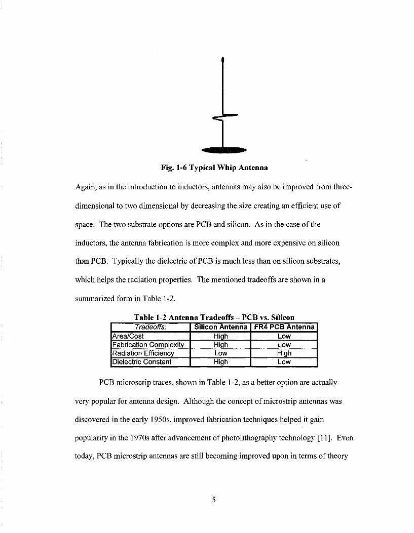
Fig. 1-6 Typical Whip Antenna
Again, as in the introduction to inductors, antennas may also be improved from three-
dimensional to two dimensional by decreasing the size creating an efficient use of
space. The two substrate options are PCB and silicon. As in the case of the
inductors, the antenna fabrication is more complex and more expensive on silicon
than PCB. Typically the dielectric of PCB is much less than on silicon substrates,
which helps the radiation properties. The mentioned tradeoffs are shown in a
summarized form in Table 1-2.
Table 1-2 Antenna Tradeoffs - PCB vs. Silicon Tradeoffs:
Area/Cost Fabrication Complexity Radiation Efficiency Dielectric Constant
Silicon Antenna High High Low High
FR4 PCB Antenna Low Low High Low
PCB microscrip traces, shown in Table 1-2, as a better option are actually
very popular for antenna design. Although the concept of microstrip antennas was
discovered in the early 1950s, improved fabrication techniques helped it gain
popularity in the 1970s after advancement of photolithography technology [11]. Even
today, PCB microstrip antennas are still becoming improved upon in terms of theory
5
and fabrication process. As a result, microstrips antennas on PCB are chosen to be
used on many portable devices for various applications.
1.2.1 Antenna Applications - GPS Background
The GPS market has grown substantially in the recent years. Due to the cost
effectiveness and portability, handheld GPS devices are popular. The idea of GPS
was invented by Ivan Getting and Bradford Parkinson during the 1950s; it is
described as a system of moving satellites that enables the determination of physical
position relative to time difference of the transmitted signals [12]. In 1969, the U.S.
Defense Department started its own research and eventually created 24 satellites,
launching them in 1978, which were operational by 1995, having capability of down
to 10 meter accuracy [13]. Although the GPS system was originally intended for
military use, due to a 1983 airline incident, President Ronald Reagan promised its
availability to civilians after its completion to promote public safety [13]. For that
reason, the general public is able to use portable GPS devices today.
An important aspect of the handheld GPS device is the antenna that ensures a
strong signal. GPS satellites send their signals on to the LI band with a carrier
frequency of 1575.42MHz and a bandwidth of 2.046MHz with RCHP, right hand
circular polarization [14]. The antenna portion of this paper will focus on the design
of a GPS application specific antenna. The proposed antenna differs from typical
GPS antennas in papers such as [15]-[17] by having a more relatively directive
radiation pattern with maximum intensity in the PCB forward direction with a theta in
6

70° range for mounting purposes. The presented antenna design is a "L-ground plane
with lowercase-h configuration and cornered patch."
1.3 Summary and Thesis Outline
The goal of the project is to create a design flow from characterizing a two
port inductor, fully characterizing the PCB board, and then designing an antenna from
the optimized simulators. This thesis is categorized into five chapters. The first
chapter is the introduction, which describes the brief background of inductors and
antennas. Chapter 2 explains the analysis and design of the inductors and the
antenna. Chapter 3 discusses the simulations that were performed for the inductors
and the antenna. Chapter 4 shows the measurements both the inductors and antenna.
Finally, chapter 5 is the conclusion, which wraps up the entire project. An important
point is that the design, simulation, and measurement for the inductor were fully
completed before the antenna's design, simulation, and measurement were
performed; however, for clear organization of the ideas, the three topics are explained
in parallel.
The result of this thesis is to create a pair of inductors with values of 55nH at
around 300MHz and lOOnH at 200MHz for intermediate frequency applications. The
first inductor, which will be denoted as inductor 'A' is an initial trial having a smaller
Q-factor goal in the range of 30, while inductor 'B' has a much higher Q-factor of at
least 50. Both inductors are to have a reasonable 3.5 turns. The completed inductors
will allow optimization of the simulators through the characterization of the PCB to
7
enable the design of an antenna centered at 1575.42MHz with a bandwidth much
greater than 2.046MHz and is right hand circularly polarized.
8
2 THEORY, ANALYSIS, AND DESIGN
This chapter will present the theory, analysis, and design of a pair of inductors
as well as an antenna. The inductor section will describe inductance, resistance, and
quality factor parameters. Following, the antenna section will describe the proposed
geometry, radiation pattern, directivity and gain, polarization, as well as impedance
bandwidth and Q-factor.
2.1 Inductor
The objective of the inductor design is to provide characteristics of a two port
component to better understand the PCB characteristics, which may also be used for
intermediate applications. Parameters such as inductance, resistance, and Q-factor
are computed and analyzed in the following sections. The goal is to create a 55nH
inductor at 300MHz with a Q-factor of around 30 and a lOOnH inductor at 200MHz
with at least a Q-factor of 50. Both inductors shall be designed with reasonable 3.5
turns. The general inductor theory regarding the inductance, resistance, and quality
factor will be presented followed with followed with specific PCB calculations.
2.1.1 Inductance
Inductors innately consist of two types of inductances: self-inductance and
mutual inductance. Both self-inductances and mutual-inductances are described in
the units of Henry. A Henry has units of Weber per Ampere, which is essentially
magnetic flux in relation to current [1]. Traditionally inductance is created through
9

coils, which is how the general definitions of mutual and self inductance will be
explained.
Mutual inductance is generated when a magnetic field is created from the
changing current of one coil which creates flux through a second adjacent coil
defined by [18]
L . - ^ - (2.D -* 1 [ 1
and vice versa,
Z , , - ^ (2.2)
The terms in the shown equations (2.1) and (2.2) are the number of turns in a coil, N,
the magnetic flux, O, and the current, I. The characteristics may be seen from the
circuit point of view where voltage is important, therefore, the induced voltage of the
two coil circuits are shown as [19]
v2 = Ln ^L (2.3) at
and
v, =L2l^-. (2.4) at
As the instantaneous current changes in one coil, a voltage in the second coil is
induced through the flux that links the two coil circuits. From analysis, mutual
inductance can be seen as a phenomenon which determines the magnitude of voltage
relative to the change in current with respect to time.
10
Self inductance is generated when a magnetic field is created from current
within a coil as opposed to (2.1) and (2.2), because the flux and current are within one
coil [18]. Self induction occurs in a coil itself and innately generates a voltage
through the flux created in an electromotive force s that is in the opposite direction,
where 8 = -L(dl/dt) [18]-[19].
These mentioned theories are for generalized cases; however, inductors can
also be analyzed for implementation on PCB.
Inductors on PCB are planar parallel to the surface of the PCB. The
inductances of PCB inductors depend specifically on the geometry. The total
inductance is determined by the mutual inductance and self inductance.
In the mentioned general inductance theory, mutual inductance was described
with two separate inductors; however, mutual inductance may also occur amongst
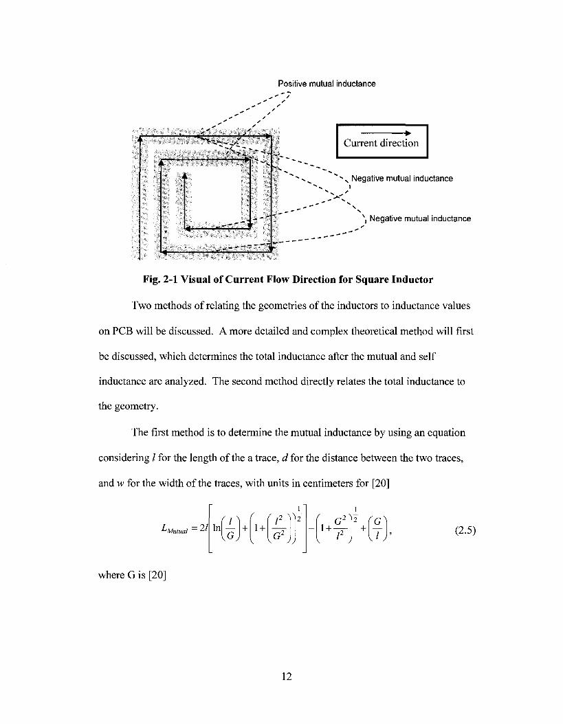
embedded parallel conductive traces within a single inductor, particularly on PCB [8].
The equations (2.1) and (2.2) can be utilized in terms of two segments within an
inductor instead of two separate inductors. In a planar PCB inductor, to calculate the
mutual inductance, the whole inductor needs to be broken up into segments and
analyzed with respect to the corresponding coupling parallel traces. The mutual
inductance may be positive or negative depending on the direction of the currents on
the parallel segments of the PCB inductor mention in [8] and [20], where the concept
is shown in the Fig. 2-1.
11
Positive mutual inductance
I—""'V - - "i"
Current direction
• s Negative mutual inductance
s, Negative mutual inductance
Fig. 2-1 Visual of Current Flow Direction for Square Inductor
Two methods of relating the geometries of the inductors to inductance values
on PCB will be discussed. A more detailed and complex theoretical method will first
be discussed, which determines the total inductance after the mutual and self
inductance are analyzed. The second method directly relates the total inductance to
the geometry.
The first method is to determine the mutual inductance by using an equation
considering / for the length of the a trace, d for the distance between the two traces,
and w for the width of the traces, with units in centimeters for [20]
-'Mutual ••21 In ' / ^
+ \^J
1 + O 2^
G1 V V " JJ
l+^V 2 (G^
+ — (2.5)
where G is [20]
12

( (f
\x\d
G = e 12
VV v w / j 60 168 360
\ ^
660 ld-\wj J
+...
J) (2.6)
The polarity of LMutuai, mutual inductance, depends on the relative current direction as
mentioned earlier in Fig 2-1.
To determine the self inductance of the particular mentioned planar inductor,
the conductive trace may be analyzed through [8]
Lself = 0.002/1 In 2/
0.2232O + /0 •1.25 +
(w + h) i f j u ^
3/ • + T
\*J (2.7)
The term ju relates to the permeability and h is the height of the PCB substrate.
Again, w is the width of the conductive trace in centimeters, and as [8] mentions, T, is
a term dependent on the thickness of the trace and frequency, that can be
approximated to be 1 for most cases [20].
Finally, the total inductance for the inductor is determined by summing all the
mutual inductances and self inductances segments in [8]
^Total — ^self ^ I ^Mutual I + ^ M u t u a l . (2.8)
As one may see, the first mentioned process of determining the geometry from
desired inductance, or vice versa, is very complicated and tedious. Therefore, the
following method is much more practical and combines the mutual and self
inductance into a single formula.
For design calculations of square planar inductors before beginning
13
simulations, the method discussed [21] is sufficient. The method calculates the
inductance in nanohenries through the equation [21]
Lsquare=%.5DN~\ (2.9)
where D is the distance between the outer edges of the square inductor, in
centimeters, and N is the number of turns within the inductor.
As mentioned earlier, two inductors designs with various values and trace
thickness will be created to have a broader view of the PCB characteristics. First a
55nH inductor denoted as 'A' will be designed followed by a lOOnH inductor denoted
as 'B.'
The distance between the outer edges of the square for inductor 'A,' DA, is
determined by first choosing the number of turns, N, to be 3 54 and setting
Lsquare=55nH. The calculation follows as:
DA * — ». 8019cw A 5
8.5(3.5)3
Since the typical units used for PCB design are in mil, which is 1/1000 on an
inch, converted, DA is 315.7 mil. In the actual layout to fit the traces, DA is set to 310
mil to accommodate the grid. Due to the fact that (2.9) only specifies the overall
square dimension and the number of turns, the width of the conductor traces are
chosen for reasonable fit within the dimension limitations. Since flexibility is
allowed for the trace width, w, and spacing between the traces, s, reasonable values of
w - 30 mil and s = 10 mil are set, as shown in Fig. 2-2.
14
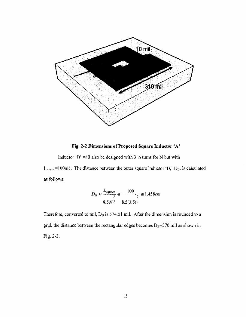
Fig. 2-2 Dimensions of Proposed Square Inductor 'A'
Inductor 'B' will also be designed with 3 lA turns for N but with
Lsquare=100nH. The distance between the outer square inductor 'B, ' DB, is calculated
as follows:
DB „ h^ s IQ0
5 s \A58cm
8.5iV3 8.5(3.5)3
Therefore, converted to mil, DB is 574.01 mil. After the dimension is rounded to a
grid, the distance between the rectangular edges becomes DB=570 mil as shown in
Fig. 2-3.
15
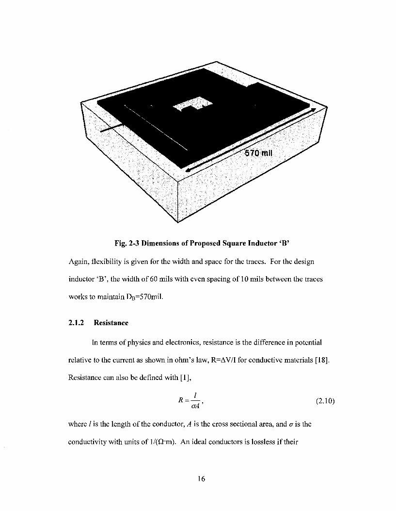
Fig. 2-3 Dimensions of Proposed Square Inductor 'B'
Again, flexibility is given for the width and space for the traces. For the design
inductor 'B' , the width of 60 mils with even spacing of 10 mils between the traces
works to maintain DB=570mil.
2.1.2 Resistance
In terms of physics and electronics, resistance is the difference in potential
relative to the current as shown in ohm's law, R=AV/I for conductive materials [18].
Resistance can also be defined with [1],
R'VA- (2-1(
where / is the length of the conductor, A is the cross sectional area, and a is the
conductivity with units of l/(£2-m). An ideal conductors is lossless if their
16
conductivity is infinitely high, however, in the real-world, conductors have losses due
to the finite conductivity.
Although the resistance at operating frequency is the interest for the inductors,
the DC resistance values are determined as a reference for comparison. The general
resistance theory is interpreted in practical equations in relation to PCB design, for
both DC and high frequencies, which will explained along with calculations.
Microstrip resistance is an important characteristic of a PCB inductor, which
changes depending on the frequency the measurements are analyzed at, either DC or
at a high frequency. At DC, derived from the (2.10), the equivalent resistance of PCB
a microstrip trace defined by [22]
/ RDC=—-, (2.11)
owt
where w, t, I, and a are the width, thickness, length, and conductivity of the
conductor, respectively.
The order of calculations for the DC resistance is first performed for the 55nH
inductor then for the lOOnH inductor. As seen in the DC resistance equation in
(2.11), the conductivity is needed for calculations. After analysis and
experimentation, the determined conductivity value used is 1.36 x 10⁶ S/m, which is
further explained in chapter 3 section 2.
The DC resistance for the 55nH inductor 'B' with 30 mil trace width
converted to 7.62xl0"4 m, and trace thickness of 1.4 mil converted to 3.556xl0"5 m,
are calculated as follows:
17
Rnc A ~ 7 1 F~~ — 2.17i2
(1.36xl06)(7.62xl0_4)(3.56xl0~5)
The DC resistance for the lOOnH inductor 'B' with the 60 mil trace width
converted to 1.52xl0"3 m, and trace thickness of 1.4 mil converted to 3.56x10"5 m is
calculated as
o coxier3 _ 2 1 2 n KDCB A IT — - 2 . 1 2 U .
(1.36xl06)(1.52xl0 3)(3.56xl0 5)
The respective DC resistances for inductor 'A' and 'B', being 2.17 Q. and 2.12
Q. intuitively make sense because inductor 'B' has wider traces, which is in
agreement with (2.10).
Importantly, the resistances are determined at the specific operating
frequencies. As frequency increases, particular to higher values, the resistance
changes because charges will swarm towards a relatively smaller area at the outer
edge of the conductor against the dielectric, with a phenomenon known as the skin
depth, which is defined as [23]
— • (2.12) ojucr
Since at high frequencies only the skin depth portion of the conductor is conductive,
intuitively the thickness term is replaced in (2.11) with the frequency dependent term
to determine resistance in
RHF= J . (2.13)
First, the resistance at operating frequency will be determined for inductor 'A'
18
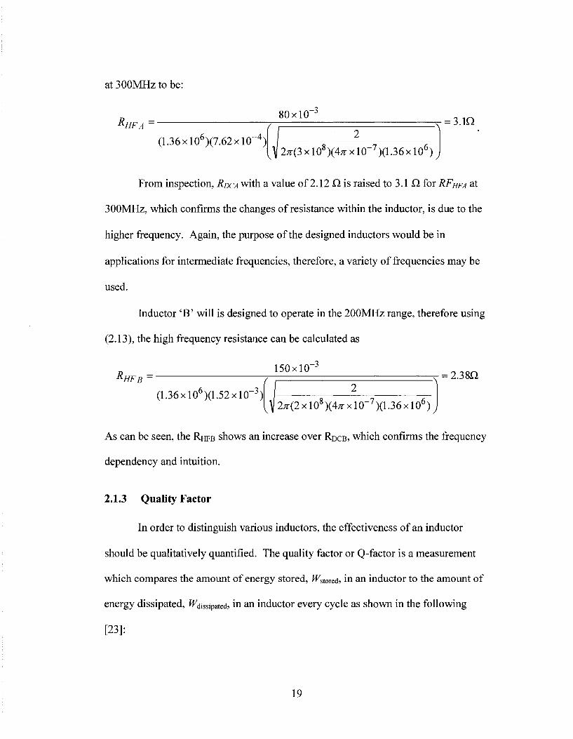
at 300MHz to be:
R 80x10 -3
HFA = 3.1Q
(1.36xl06)(7.62xl0~4) 2;z-(3xl08)(4;rxl0~7)(1.36xl06)
From inspection, RDCA with a value of 2.12 Q. is raised to 3.1 Q. for RFHFA at
300MHz, which confirms the changes of resistance within the inductor, is due to the
higher frequency. Again, the purpose of the designed inductors would be in
applications for intermediate frequencies, therefore, a variety of frequencies may be
used.
Inductor 'B' will is designed to operate in the 200MHz range, therefore using
(2.13), the high frequency resistance can be calculated as
R 150x10"
HFB = 2.38Q
(1.36xl06)(1.52xl0~3) 2^(2 x 10⁸ )(4TT x 10~7 )(1.36 x 10⁶)
As can be seen, the RHFB shows an increase over RDCB, which confirms the frequency
dependency and intuition.
2.1.3 Quality Factor
In order to distinguish various inductors, the effectiveness of an inductor
should be qualitatively quantified. The quality factor or Q-factor is a measurement
which compares the amount of energy stored, Stored* m a n inductor to the amount of
energy dissipated, d̂issipated, in an inductor every cycle as shown in the following
[23]:
19

Q _ —stored (freqUenCy _ dependency) Q \ 4) dissipated
In terms of the components, the quality factor may also be represented in
terms of the resistance, R, and inductance, L, by [21]
Q-— (2.15)
where the frequency dependency can be seen. However, the Q-factor is typically
evaluated at a frequency is far below resonant [24]. The Q-factors for the two
inductors are determined. The Q-factor of an inductor 'A' with an inductance of
55nH and a resistance of 3.1 Q. at a frequency of 300MHz is computed as follows:
_ 2^(300 X 1 0 6 ) ( 5 5 X 1 Q - 9 ) _ 3 3 1
A 3.10 ' '
The quality factor for the inductor 'B' 200MHz design with the corresponding
calculated resistance of 2.38 Q and lOOnH inductor parameter is computed as
follows:
n 2^(200 x 106 )(100 xl(T9) UD — — 52.8 *B 2.38
The quality factor for inductor 'B' is 53, which is reasonably high.
2.2 Antenna
The proposed antenna project is a GPS patch. A brief overview of GPS
technology follows.
Technically, GPS has two services, the Precise Positioning Service for the
20

military and the Standard Positioning Service, SPS, which is less accurate, but still
very effective for civilians [14]. SPS transmits messages on to the LI signal at the
carrier frequency 1575.42MHz with a bandwidth of 2.046MHz with right hand
circular polarization [14]. This project will focus on the LI civilian frequency.
The subsections for the antennas design will include the proposed geometry, a
brief description of radiation pattern, directivity compared to gain, polarization, and
impedance bandwidth compared to Q-factor.
2.2.1 Proposed Geometry
A starting point to design a reasonable small antenna is the classic inverted-f
[25]-[26], known for its compactness. After analyzing the parameters such as
polarization and radiation patterns, a modified antenna is design is proposed. The
proposed unique antenna, "L-ground plane with lowercase-h configuration and
cornered patch," is shown in Fig. 2-4.
21
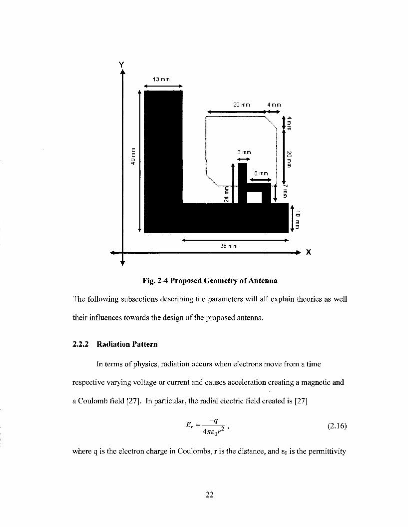
13 mm
e E
36 mm • * X
Fig. 2-4 Proposed Geometry of Antenna
The following subsections describing the parameters will all explain theories as well
their influences towards the design of the proposed antenna.
2.2.2 Radiation Pattern
In terms of physics, radiation occurs when electrons move from a time
respective varying voltage or current and causes acceleration creating a magnetic and
a Coulomb field [27]. In particular, the radial electric field created is [27]
E = -q
AnsQr 2 ' (2.16)
where q is the electron charge in Coulombs, r is the distance, and so is the permittivity
22
of free space. The fields influence the radiation patterns, which will be explained in
detail.
Radiation patterns define an antenna's electric field characteristics. It is
important to determine the unique far-field characteristics of an antenna. One method
to determine the radiation pattern is based on the electric surface current model,
which for rectangular patches would be [11]
E0(0,0) = sin<M An -r
e ° {CurrentChar)(GndEff) (2.17)
Ee(6,(/)) = -cos(/> J-^- e J °r {CurrentCha-)(GndEff) yAn-r J
(2.18)
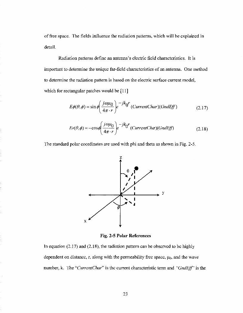
The standard polar coordinates are used with phi and theta as shown in Fig. 2-5.
Fig. 2-5 Polar References
In equation (2.17) and (2.18), the radiation pattern can be observed to be highly
dependent on distance, r, along with the permeability free space, u.o, and the wave
number, k. The "CurrentChar" is the current characteristic term and "GndEff is the
23

ground effects term. Both mentioned terms are related to the polar coordinates and
are highly dependent on the antenna's geometry.
In terms of the proposed design, the left vertical side of the "L" shaped ground
plane along the Y axis in Fig. 2-4 acts as a unique reflector to create a strong front
beam in the +X direction, which dictates a particular desired radiation pattern.
The theory of the far-field radiation patterns can be found by finding the limit
of the electric or magnetic field to infinity, such as [28]
E(r -» 00,0,0) = Efarfield{0,(/>)—- (2.i9)
and
H(r -> oo, 9, </>) = Hfarfield (<9, (/>) , (2.20)
where the distance, r, can be seen to have a large influence with the electric and
magnetic fields.
2.2.3 Directivity and Gain
Directivity and Gain are related to maximum radiation density. Directivity is
the concentration of radiation intensity relative to the average radiated power,
described in polar coordinates in [28]
An m a X 2 (Efarfield ^ ' ^ * Hfarf'eld * (0> 0)))
W > 0 = — T7 - • (2-21)
\l Q hfarfield X Hfarfield * ' ^
Essentially, the denominator is the average radiated power through the Poynting
24
vector [29], in Watts, which is similar to determining the gain [28] in
f An max - [EMield (O, (f)x Hfarfield * (G, M
G(0J) = - ^ ^ H, (2.22) input
The gain relates the maximum intensity to the input power instead. The variation
between the gain compared to the directivity is due to the loss, which the efficiency,
e, may be determined in [28]
D{e 4) • (2-23)
The efficiency is essentially the ratio of the gain to the directivity.
The directivity desired for the proposed specific design is to have the main
beam at phi = 0°, which is achieved by the reflector reflecting the fields in the
opposite 180° direction, creating the intense forward zero degrees phi power.
2.2.4 Polarization
Antennas also can be characterized by a polarization behavior. Polarization is
a characteristic of the EM waves in regards to the varying vector positions with
respect to time [29]. A linear polarization implies that the waves move in a straight
line when seen in a two dimensional view. Therefore a linear electrical field vector
moving along the x-axis and propagating respect to time on the z-axis may be shown
as [29]
E = aXe-Jkz, (2.24)
where k is the wavenumber that is dependent on the wavelength defined as k=2n/X.
25
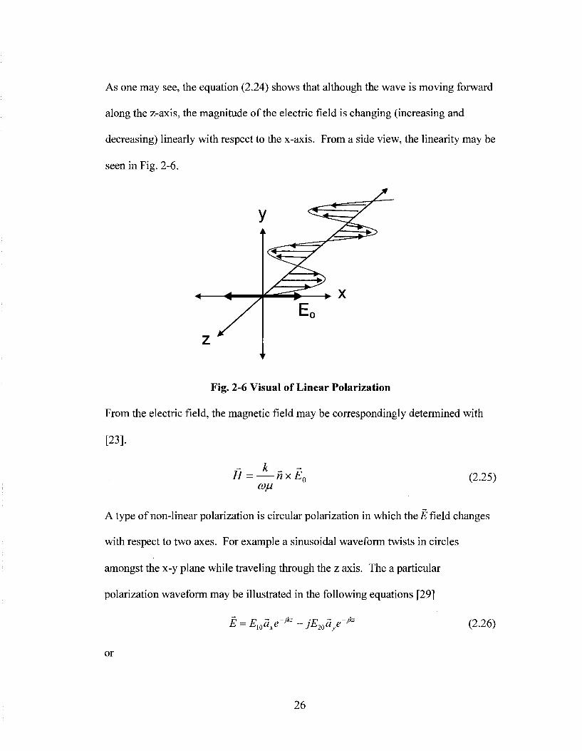
As one may see, the equation (2.24) shows that although the wave is moving forward
along the z-axis, the magnitude of the electric field is changing (increasing and
decreasing) linearly with respect to the x-axis. From a side view, the linearity may be
seen in Fig. 2-6.
Fig. 2-6 Visual of Linear Polarization
From the electric field, the magnetic field may be correspondingly determined with
[23].
H = nxE0 (2.25) coju
A type of non-linear polarization is circular polarization in which the E field changes
with respect to two axes. For example a sinusoidal waveform twists in circles
amongst the x-y plane while traveling through the z axis. The a particular
polarization waveform may be illustrated in the following equations [29]
E = Ewaxe-Jkz-jE2Qaye-jk* (2.26)
or
26
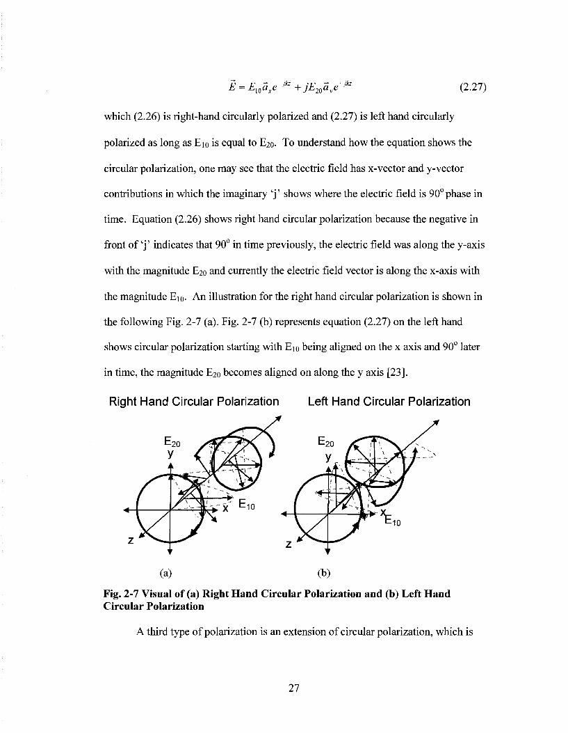
E = Ewaxe-jk2+jE20aye-jh (2.27)
which (2.26) is right-hand circularly polarized and (2.27) is left hand circularly
polarized as long as Eio is equal to E20. To understand how the equation shows the
circular polarization, one may see that the electric field has x-vector and y-vector
contributions in which the imaginary ' j ' shows where the electric field is 90° phase in
time. Equation (2.26) shows right hand circular polarization because the negative in
front of ' j ' indicates that 90° in time previously, the electric field was along the y-axis
with the magnitude E20 and currently the electric field vector is along the x-axis with
the magnitude Eio. An illustration for the right hand circular polarization is shown in
the following Fig. 2-7 (a). Fig. 2-7 (b) represents equation (2.27) on the left hand
shows circular polarization starting with Eio being aligned on the x axis and 90° later
in time, the magnitude E20 becomes aligned on along the y axis [23].
Right Hand Circular Polarization Left Hand Circular Polarization
(a) (b)
Fig. 2-7 Visual of (a) Right Hand Circular Polarization and (b) Left Hand Circular Polarization
A third type of polarization is an extension of circular polarization, which is
27

the elliptical polarization. This occurs when the magnitudes of the electric field, Eio
and E20, are not equal [29].
Particular to the proposed antenna, a linear electrical field vector moving up
and down on the y-axis moving while propagating in the z-axis with respect to time is
shown as [29]
E = ayE+
0e~Jh (2.28)
which is an innate characteristic of the "lower case-h" portion of the antenna without
the cornered square patch in Fig. 2-4. Due to the modification of the antenna, the
straight portion of the "h" became the A/8 wavelength feed into the patch.
The GPS signals are sent with right hand circular polarization [14], as
mentioned earlier. In order to provide a design with circular polarization, a few
methods may be used such as having a dual feeds 90° out of phase fed into a patch, a
single modified feed patch, a square patch with rectangular slot, or removing two
opposite corners of a square patch as shown in Fig. 2-8 [30]-[31],
v AS
z
Feed
AS
Single Diagonal Feed Diagonal Slot Removed Corners
0 = Feed point
Fig. 2-8 Various Circular Polarization Patch Methods
As can be seen in Fig. 2-8 the last method on the right is used. The amount of
28

conductor removed, AS, from the total patch area, S, depends on the circular
polarization due to the desired unloaded Q-factor in the equation [11]
AS 1
The Q-factor for antennas will be described in section 2.5.
The phenomenon of the circular polarization of the chosen patch is explained.
Removing of the two corners of the square patch creates a 90° phase shift from the
exited wave mode by creating a two ends with less capacitive corners distinguishing
the waves from the more capacitive corners [30]. The mentioned right-hand
circularly polarized is illustrated with the following equation [23]
E = EQ(az-jay)e-jkx (2.30)
because, again, the negative in front of ' j ' indicates that 90° previously in phase time,
the signal was aligned with the z-axis, which then becomes aligned to the y-axis. The
order of the signal shows the clockwise movement in the right hand direction, while
propagating in the +X direction.
2.2.5 Impedance Bandwidth and Q-factor
The bandwidth of an antenna is the frequencies in which the antenna is
optimized to be used in. This section will show the tradeoff between impedance
bandwidth and the quality factor.
The impedance seen into the antenna can have an imaginary part due to the
capacitive or inductive nature and a real part which is pure resistance. The difference
in the impedance creates a reflection of the signal and can be measured by [31]
29
r = ^ ^ , (2.3i) Zin + Zn '0
which Zin is the input impedance and the Zo is the characteristic impedance. Ideally,
the smaller the reflection coefficient, the better the power is transferred from one
stage to the next. Also, optimal matching results in a smaller reflection coefficient.
From the reflection coefficient, the VSWR may be determined. The VSWR is
the voltage standing-wave ratio (the relation between the maximum voltage to the
minimum voltage) is a real number between one and infinite, which a 'one' value
means a perfect match and that none of the signal is reflected [31]. The VSWR is an
indication of how well components are matched, which may be determined from the
reflection coefficient in the equation [22],
VSWR = ^ ^ - . (2.32) 1- | T |
After determining the VSWR, the impedance bandwidth, which is the portion of the
frequency spectrum that is expected to be well matched, may be determined in [32]
BW_VSWR± Qy/VSWR
where Q is the quality factor of the antenna. In the analysis of equation (2.33), the
bandwidth, BW, is inversely proportional to the quality factor, Q, which is a tradeoff.
The quality factor is a measure of an antenna's physical limitation and performance
which can be determined through [30]
Q = ~r> (2-34)
30
where Wis the energy stored during resonance and P is the power loss.
In detail, other factors that affect the Q-factor are the radiator shape, the
substrate thickness, the dielectric, and the losses of the conductors [11]. The Q-factor
relation to the mentioned factors from [11] can be shown in a detailed Q-factor
expression
QT = j _ j _ j _ , (2.35)
Qc + Qd + QR
where the Qd term is the contribution of the Q-factor through the dielectric materials
of the PCB in [30]
2-7T-£r-£Q-f
Qd= , (2.36)
ad
with the s dielectric term, t h e / the frequency term, and Od the bulk conductivity term.
The Qc is the Q-factor contribution through the conductor loss, where [30]
Qc =h^ju0-7r-f-a . (2.37)
The h in (2.37) is the height in mm, the juo is the permeability of free-space, the a is
the conductivity of the conductor, while/frequency of interest. In general, the QR
term refers to the radiation Q-factor as in (2.34). Essentially the contributions of the
inverses of Qc and Qd are so small, unlike Q=QR, which is larger [11].
With the general theory of impedance bandwidth for the antenna discussed,
the specific impedance bandwidth of an antenna may be calculated.
Again, the impedance bandwidth relates to the frequencies in which the
antenna signal may transfer power optimally within reasonable impedance match.
31
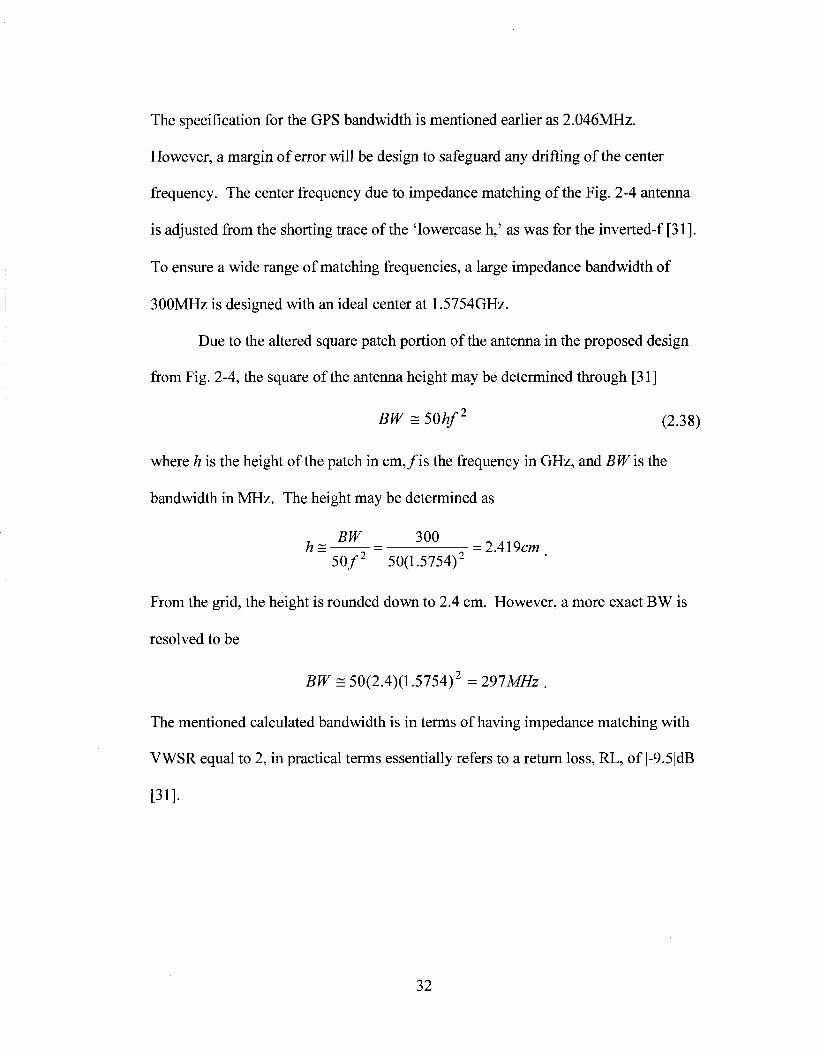
The specification for the GPS bandwidth is mentioned earlier as 2.046MHz.
However, a margin of error will be design to safeguard any drifting of the center
frequency. The center frequency due to impedance matching of the Fig. 2-4 antenna
is adjusted from the shorting trace of the 'lowercase h,' as was for the inverted-f [31].
To ensure a wide range of matching frequencies, a large impedance bandwidth of
300MHz is designed with an ideal center at 1.5754GHz.
Due to the altered square patch portion of the antenna in the proposed design
from Fig. 2-4, the square of the antenna height may be determined through [31]
BW = 50hf2 (2.38)
where h is the height of the patch in cm, / i s the frequency in GHz, and BW is the
bandwidth in MHz. The height may be determined as
, BW 300 n / l i n
h = = = 2.419cw 5 0 / 2 50(1.5754)2
From the grid, the height is rounded down to 2.4 cm. However, a more exact BW is
resolved to be
BW = 50(2.4)(1.5754)2 = 291 MHz .
The mentioned calculated bandwidth is in terms of having impedance matching with
VWSR equal to 2, in practical terms essentially refers to a return loss, RL, of |-9.5|dB
[31].
32
2.3 Chapter Summary
The inductor theory and analysis has given the background necessary for the
design. The two calculation methodologies behind the inductor design were shown,
which led to practical calculations. Also, the antenna section described the design
methodology as well as the calculation behind the design. Although the antenna
design began after the inductors were fully designed, fabricated, and tested, the
antenna design is written in this chapter for organization to show the parallels
amongst the ideas. The hand calculations that are performed needs to be validated
through simulation, which is presented in the next chapter.
33
3 SIMULATIONS
Simulations are important to verify the calculations and analysis in chapter 2.
The simulations would show if the design approximations are feasible. The two
simulators that are used are ADS and Sonnet, both softwares are specialized in radio
and microwave frequency circuit and components. First the simulations of the two
designed inductors are performed and after analysis, the antenna simulations are
performed.
3.1 Inductors
In order to simulate the inductors that were designed, layouts must be created in
the design tools.
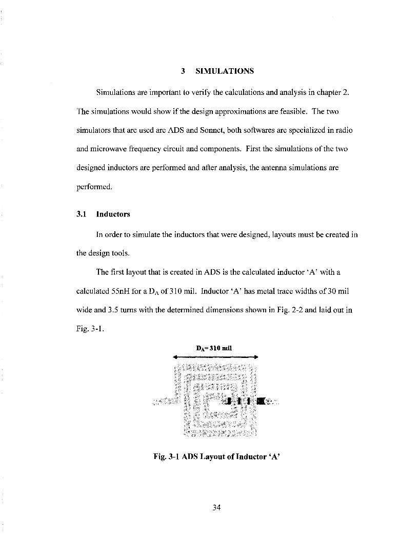
The first layout that is created in ADS is the calculated inductor 'A' with a
calculated 55nH for a DA of 310 mil. Inductor 'A' has metal trace widths of 30 mil
wide and 3.5 turns with the determined dimensions shown in Fig. 2-2 and laid out in
Fig. 3-1.
D A = 3 I 0 H U 1
•4 •
I | i m-.<
Fig. 3-1 ADS Layout of Inductor 'A'
34
In Fig. 3-1, the square spiral is drawn with top layer metal with a copper alloy
described more in detail in chapter 3 section 2. The small portion near the right feed
trace is a bottom trace, which is a necessary bridge underpass to link the two ports of
the inductor. Also, two vias are needed to complete the inductor for the two layers.
These mentioned characteristics also apply to all the layouts for the inductors in this
section.
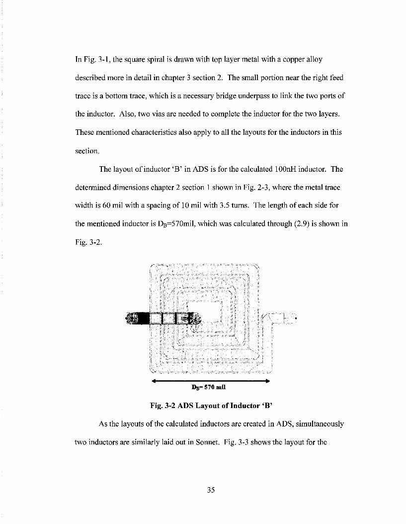
The layout of inductor 'B' in ADS is for the calculated lOOnH inductor. The
determined dimensions chapter 2 section 1 shown in Fig. 2-3, where the metal trace
width is 60 mil with a spacing of 10 mil with 3.5 turns. The length of each side for
the mentioned inductor is DB=570mil, which was calculated through (2.9) is shown in
Fig. 3-2.
-4 • Dg,= 570mi l
Fig. 3-2 ADS Layout of Inductor 'B'
As the layouts of the calculated inductors are created in ADS, simultaneously
two inductors are similarly laid out in Sonnet. Fig. 3-3 shows the layout for the
35
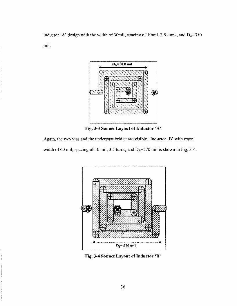
inductor 'A' design with the width of 30mil, spacing of lOmil, 3.5 turns, and DA=310
mil.
Fig. 3-3 Sonnet Layout of Inductor 'A'
Again, the two vias and the underpass bridge are visible. Inductor 'B' with trace
width of 60 mil, spacing of 10 mil, 3.5 turns, and DB=570 mil is shown in Fig. 3-4.
fcfi DB=570HU1
Fig. 3-4 Sonnet Layout of Inductor 'B'
36
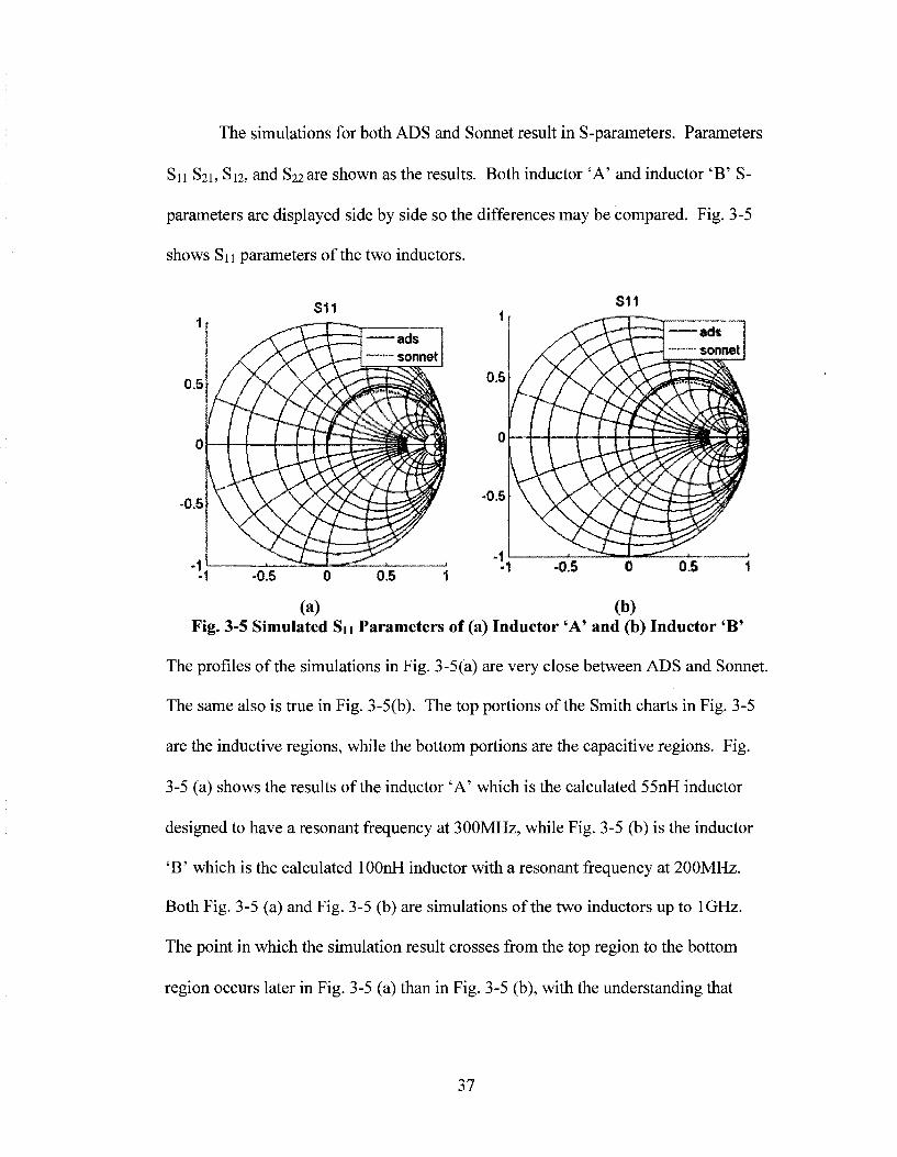
The simulations for both ADS and Sonnet result in S-parameters. Parameters
Sn S21, S12, and S22are shown as the results. Both inductor 'A' and inductor 'B' S-
parameters are displayed side by side so the differences may be compared. Fig. 3-5
shows Sn parameters of the two inductors.
(a) (b)
Fig. 3-5 Simulated Sn Parameters of (a) Inductor 'A' and (b) Inductor 'B'
The profiles of the simulations in Fig. 3-5(a) are very close between ADS and Sonnet.
The same also is true in Fig. 3-5(b). The top portions of the Smith charts in Fig. 3-5
are the inductive regions, while the bottom portions are the capacitive regions. Fig.
3-5 (a) shows the results of the inductor 'A' which is the calculated 55nH inductor
designed to have a resonant frequency at 300MHz, while Fig. 3-5 (b) is the inductor
'B' which is the calculated lOOnH inductor with a resonant frequency at 200MHz.
Both Fig. 3-5 (a) and Fig. 3-5 (b) are simulations of the two inductors up to 1GHz.
The point in which the simulation result crosses from the top region to the bottom
region occurs later in Fig. 3-5 (a) than in Fig. 3-5 (b), with the understanding that
37
both frequency limits are the same. Fig. 3-5 (a) and Fig. 3-5 (b) simulation results are
expected.
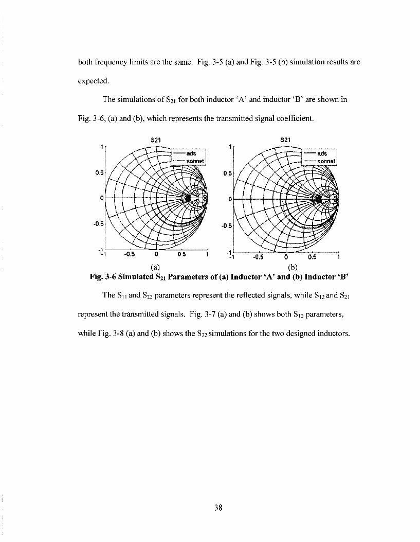
The simulations of S21 for both inductor 'A' and inductor 'B' are shown in
Fig. 3-6, (a) and (b), which represents the transmitted signal coefficient.
Fig. 3-6 Simulated S21 Parameters of (a) Inductor 'A' and (b) Inductor 'B'
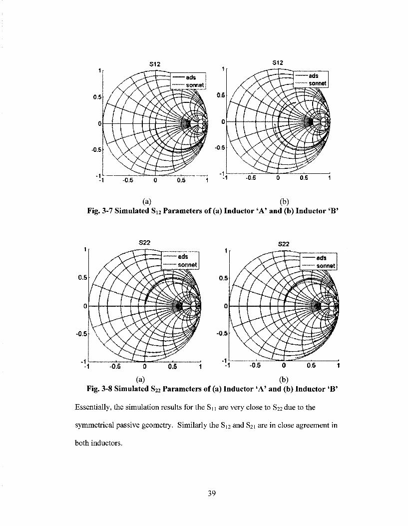
The Sn and S22 parameters represent the reflected signals, while S12 and S21
represent the transmitted signals. Fig. 3-7 (a) and (b) shows both S12 parameters,
while Fig. 3-8 (a) and (b) shows the S22 simulations for the two designed inductors.
38
1
0,5
0
0.5
4
S12
\ \ LA-xv55
^SI , *""•—-L f ——
ads sonnet
JT30ZW
• ^ ,
1r
0.5
0
•0.5
<
S12 - H - ^ ^ T ~^*^
f \\ 1 „_«A-—
- . — a £ j s
"• sonnet
""""̂ .
-1 -0,5 0.5 -0.5 0.5
(a) (b) Fig. 3-7 Simulated S12 Parameters of (a) Inductor 'A' and (b) Inductor 'B'
1
0.5
0
-0.5
• ! •
[ ^
(m i f i
\ IL-V \ ^
^ ^ -0.5
S22
./0\$c
ads sonnet
0 0.5 i
S22
(a) (b)
Fig. 3-8 Simulated S22 Parameters of (a) Inductor 'A' and (b) Inductor 'B'
Essentially, the simulation results for the Si 1 are very close to S22 due to the
symmetrical passive geometry. Similarly the S12 and S21 are in close agreement in
both inductors.
39
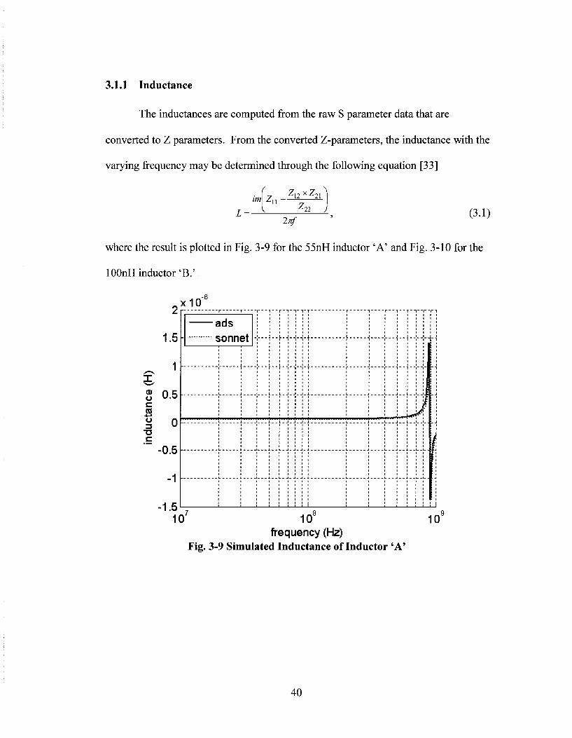
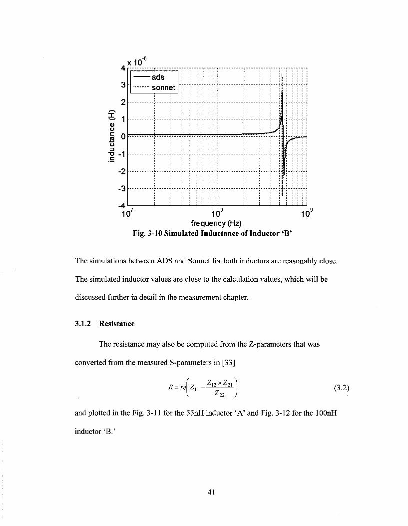
3.1.1 Inductance
The inductances are computed from the raw S parameter data that are
converted to Z parameters. From the converted Z-parameters, the inductance with the
varying frequency may be determined through the following equation [33]
im Zn x ^2i
-^22 )
2nf (3.1)
where the result is plotted in Fig. 3-9 for the 55nH inductor 'A' and Fig. 3-10 for the
lOOnH inductor 'B.'
2
1.5
1
m 0.5
x10
u c CO
-•-•
o 0
-0.5
-1
•1.5
ni - l i -
ads sonnet -
— !_- -£
I I : I ! i I : i
L***«
I
J 1/ 1 i : : i
10' 10° frequency (Hz)
Fig. 3-9 Simulated Inductance of Inductor 'A'
10'
40
4
3
2
£ 1 o
o
i-1
-2
-3
-4
x10"6
Q j „
aas sonnet "
\- ;----
I- ;
! i
: : : : : ; : i 1 ij
! : ! ! ! : I i i i;
!|!M| i i a
" t i i :
1 I ' I > 1 1 1 ' 1 H
! ! ! ! ! ! ! ! ! !
i- -j.
I 10' 10°
frequency (Hz) Fig. 3-10 Simulated Inductance of Inductor 'B'
10a
The simulations between ADS and Sonnet for both inductors are reasonably close.
The simulated inductor values are close to the calculation values, which will be
discussed further in detail in the measurement chapter.
3.1.2 Resistance
The resistance may also be computed from the Z-parameters that was
converted from the measured S-parameters in [33]
R = re\ Z12 xZ2 ,
•^22 J (3.2)
and plotted in the Fig. 3-11 for the 55nH inductor 'A' and Fig. 3-12 for the lOOnH
inductor 'B.'
41
£ sz
O
c
"w 0)
16000
14000
12000
10000
8000
6000
4000
2000
1 ads
sonnet
1
. _ L
. _ L
. _ L
:
• 1 •
10' 10° frequency (Hz)
Fig. 3-11 Simulated Resistance of Inductor 'A'
10^
2.5 x10
° 1.5 0)
u c
0.5
0
ads sonnet
i
...\.
Ji L_ __LLi 10' 10
frequency (Hz) Fig. 3-12 Simulated Resistance of Inductor 'B'
10°
42
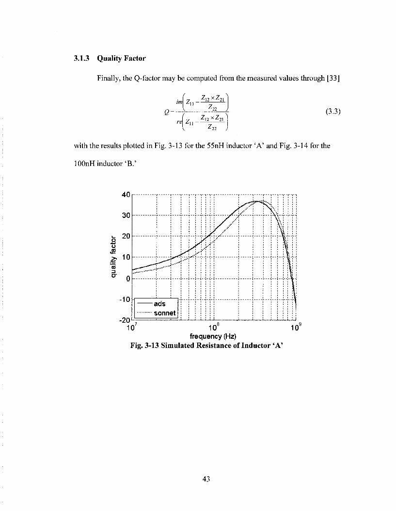
3.1.3 Quality Factor
Finally, the Q-factor may be computed from the measured values through [33]
im\
Q
Zu-Z12 x Z21
V J22 J
re\Zn-ZnXZl^ V
(3.3)
-22 J
with the results plotted in Fig. 3-13 for the 55nH inductor 'A' and Fig. 3-14 for the
lOOnH inductor 'B.'
40
30
o 2 0
o JS
£ 10
(0 3
-10
-20
I
: i
j
ads sonnet
!- - - i - - J- - -I- -!- -I- i -y^- -i"- 1
1 . 1 L / t 1 If" 1 1
i i > k T : . ^ i i i i if'-i >. J . _• _ i i J
!••*" 1 1 1 1 1 I i I
i i i ; i i i ;
! I \ i ! !
i i i \ v i
i _ _ i _ _>_ . k _'_.
: : : : !
10 10 frequency (Hz)
Fig. 3-13 Simulated Resistance of Inductor 'A'
10°
43
60
40
20
a o (J
£ -20
g- -40
-60 f-
-80
-100
ads sonnet
.iiiii.Lr^ JM
L . - _ L - J - - t - J - L
i I i : : i
^
\
— -
----
\ >
--"
H
>
_ j _ j _ i
. j _ j _ i
\\ ! j
" V 'J \
! ! i
10' 10" frequency (Hz)
Fig. 3-14 Simulated Resistance of Inductor 'B'
103
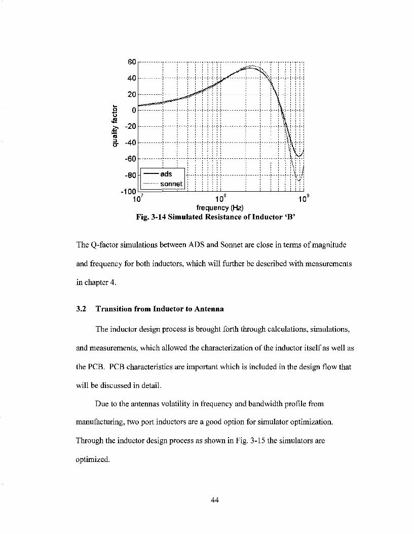
The Q-factor simulations between ADS and Sonnet are close in terms of magnitude
and frequency for both inductors, which will further be described with measurements
in chapter 4.
3.2 Transition from Inductor to Antenna
The inductor design process is brought forth through calculations, simulations,
and measurements, which allowed the characterization of the inductor itself as well as
the PCB. PCB characteristics are important which is included in the design flow that
will be discussed in detail.
Due to the antennas volatility in frequency and bandwidth profile from
manufacturing, two port inductors are a good option for simulator optimization.
Through the inductor design process as shown in Fig. 3-15 the simulators are
optimized.
44
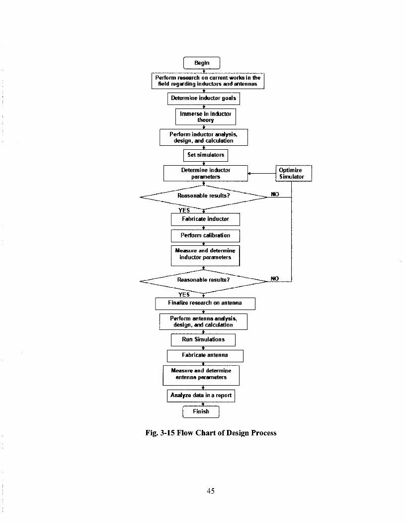
I Begin I
Perform research on current works in the field regarding inductors and antennas
* " Determine inductor goals
Immerse in inductor theory
• Perform inductor analysis,
design, and calculation
Set simulators
I Determine inductor
parameters
Reasonable results?
YES -r~~^~ Fabricate inductor
+ Perform calibration
+ Measure and determine
inductor parameters
Reasonable results?
Optimize Simulator
~~~^=> M O
- — - _ MO
Y E S T Finalize research on antenna
* Perform antenna analysis, design, and calculation
* Run Simulations
Fabricate antenna
Measure and determine antenna parameters
+ Analyze date in a report
Finish
Fig. 3-15 Flow Chart of Design Process
45
Although the inductors design, fabrication, and measurements are in series to the
antenna, this paper explains them in parallel for organization purposes. The flow
chart of the proposed design process explains in detail the procedures that are
performed. After the whole inductor design flow, inductor characteristics are
determined to be used for the antenna design.
The dielectric constant of the FR4 is refined experimentally to be £r of 3.8. The
specified thickness of the substrate is 62.5 mil and the conductor trace thickness 1.4
mil is experimentally determined to be an accurate representation. The original
simulations were based on the theoretical conductivity of pure copper to be 5.8x10⁷
S/m [23], however through the inductor design flow, as shown in Fig. 3-15, it was
discovered that the value was a lower than expected 1.36 x 10⁶ S/m that is found to be
optimal for the simulations. With the PCB characteristics determined, the antenna
design began.
3.3 Antenna
The simulations for the antenna will begin first with the radiation pattern,
directivity and gain, polarization, and impedance bandwidth.
3.3.1 Radiation Pattern
The radiation pattern of the E-field in the phi plane is shown in following
figure Fig. 3-16.
46
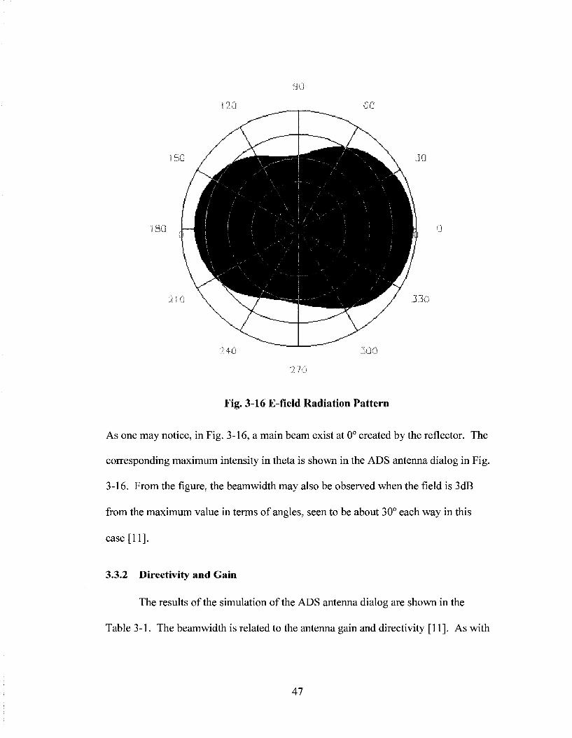
Fig. 3-16 E-field Radiation Pattern
As one may notice, in Fig. 3-16, a main beam exist at 0° created by the reflector. The
corresponding maximum intensity in theta is shown in the ADS antenna dialog in Fig.
3-16. From the figure, the beamwidth may also be observed when the field is 3dB
from the maximum value in terms of angles, seen to be about 30° each way in this
case [11].
3.3.2 Directivity and Gain
The results of the simulation of the ADS antenna dialog are shown in the
Table 3-1. The beamwidth is related to the antenna gain and directivity [11]. As with
47
intuition, beam width is inversely proportional to the gain and directivity, which is
high due to the relatively small beamwidth from the previous section.
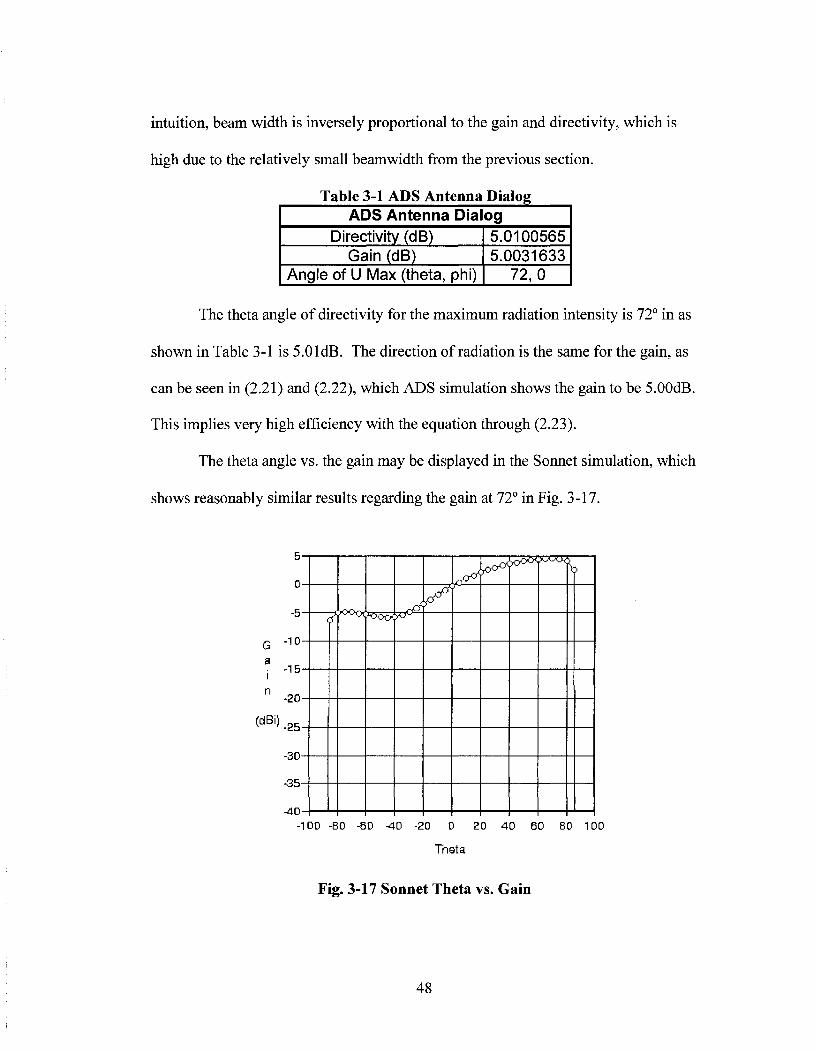
Table 3-1 ADS Antenna Dialog ADS Antenna Dialog
Directivity (dB) Gain (dB)
Angle of U Max (theta, phi)
5.0100565 5.0031633
72,0
The theta angle of directivity for the maximum radiation intensity is 72° in as
shown in Table 3-1 is 5.01dB. The direction of radiation is the same for the gain, as
can be seen in (2.21) and (2.22), which ADS simulation shows the gain to be 5.00dB.
This implies very high efficiency with the equation through (2.23).
The theta angle vs. the gain may be displayed in the Sonnet simulation, which
shows reasonably similar results regarding the gain at 72° in Fig. 3-17.
a i n
(dBi|
-15
-20
-25
-30
-35
-40
a o<x>o<
rtXW ho^
-100 -80 -60 -40 -20 0 20 40 60 80 100
Theta
Fig. 3-17 Sonnet Theta vs. Gain
48
For the design of a portable GPS handheld antenna mounted within the car,
the theta angle allows sight to the sky.
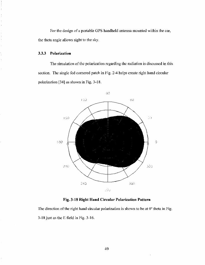
3.3.3 Polarization
The simulation of the polarization regarding the radiation is discussed in this
section. The single fed cornered patch in Fig. 2-4 helps create right hand circular
polarization [34] as shown in Fig. 3-18.
Fig. 3-18 Right Hand Circular Polarization Pattern
The direction of the right hand circular polarization is shown to be at 0° theta in Fig.
3-18 just as the E field in Fig. 3-16.
49
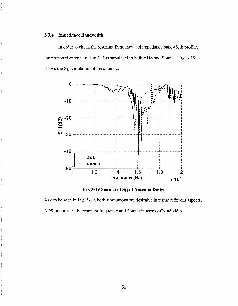
3.3.4 Impedance Bandwidth
In order to check the resonant frequency and impedance bandwidth profile,
the proposed antenna of Fig. 2-4 is simulated in both ADS and Sonnet. Fig. 3-19
shows the S n simulation of the antenna.
1.4 1.6 frequency (Hz) x 1 0
Fig. 3-19 Simulated Sn of Antenna Design
As can be seen in Fig. 3-19, both simulations are desirable in terms different aspects,
ADS in terms of the resonant frequency and Sonnet in terms of bandwidth.
50

3.4 Chapter Summary
The simulations show that the design methodology used in chapter 2 were in
the correct direction for both the inductors and antenna designs. An important section
is the 'Transition from Inductor to Antenna,' which is chapter 3 section 2 because the
complete design flow is presented in Fig. 3-15. As mentioned in the flow, the next
step is to fabricate and measure the designs, which leads to chapter 4,
'Measurements.'
51
4 MEASUREMENTS
This chapter will cover the conditions of measurements, the calibration and de-
embedding, and the measurements for the inductors and antennas.
4.1 Measurement Conditions
To be clear, due to the available resources, the measurements were not
performed in an anechoic chamber. Also, the measurements were not performed
within an absorbing material box. The measurements were performed in a standard
lab environment. Typical ambient environment atmosphere are to be considered with
the measurement results.
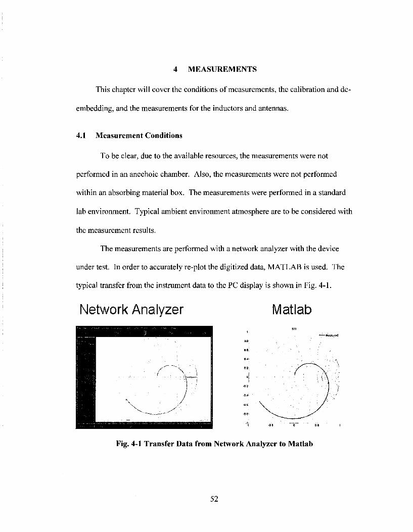
The measurements are performed with a network analyzer with the device
under test. In order to accurately re-plot the digitized data, MATLAB is used. The
typical transfer from the instrument data to the PC display is shown in Fig. 4-1.
Network Analyzer Matlab
Fig. 4-1 Transfer Data from Network Analyzer to Matlab
52
4.2 Calibration and De-embedding
For the most accurate results in measurements, both calibration and de-
embedding are needed and are discussed in the two following sections.
4.2.1 VNA and Calibration
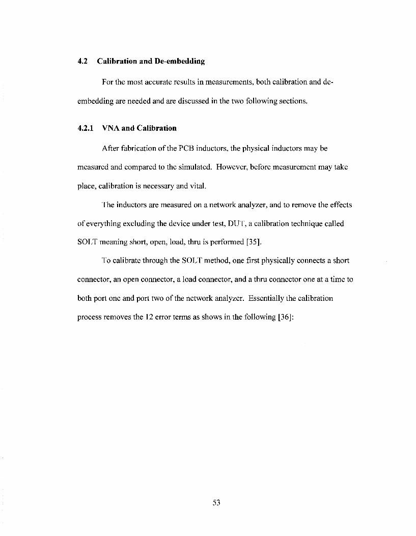
After fabrication of the PCB inductors, the physical inductors may be
measured and compared to the simulated. However, before measurement may take
place, calibration is necessary and vital.
The inductors are measured on a network analyzer, and to remove the effects
of everything excluding the device under test, DUT, a calibration technique called
SOLT meaning short, open, load, thru is performed [35].
To calibrate through the SOLT method, one first physically connects a short
connector, an open connector, a load connector, and a thru connector one at a time to
both port one and port two of the network analyzer. Essentially the calibration
process removes the 12 error terms as shows in the following [36]:
53
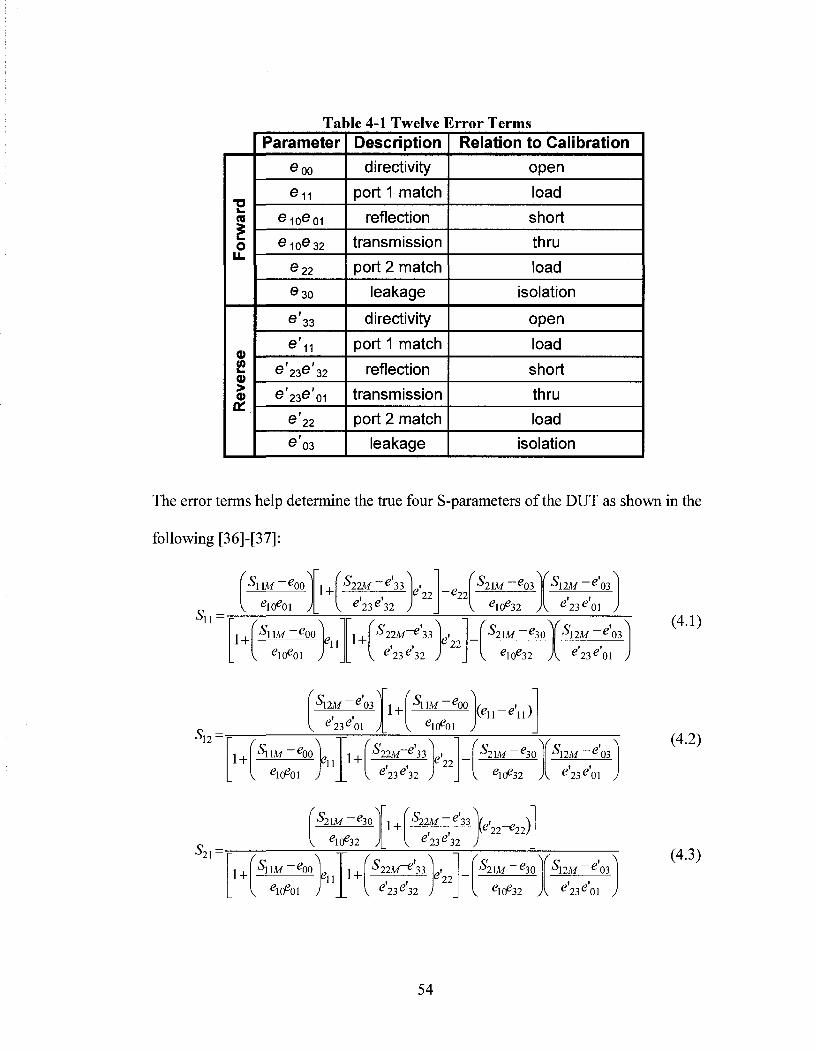
Table 4-1 Twelve Error Terms
Fo
rwar
d
Rev
erse
Parameter eoo e n
e 1 0 e 0 1
e 1 0 e 3 2
e 2 2
e 3 0
e ' 33
e n e 2 3 e ' 3 2
e ' 2 3 e ' o i
e 22
e ' o3
Description
directivity
port 1 match
reflection
transmission
port 2 match
leakage
directivity
port 1 match
reflection
transmission
port 2 match
leakage
Relation to Calibration
open
load
short
thru
load
isolation
open
load
short
thru
load
isolation
The error terms help determine the true four S-parameters of the DUT as shown in the
following [36]-[37]:
S,,=
*$! XM g00
g10g01 1 + >22M g 33
V e ' 2 3 e 3 2 J •22 ^22
$21M ~ g 0 3
. ^ 3 2 ,
Sl2M~e'o3
. g ' 23 g ' o i J
1 + ^ l l M ~ g 0 0
g10g01 j
g l l 1 + ^22M g 3 3
V g 2 3 g 3 2 J
g 2 2 ^21M ~ g 3 0 V
V glOg32 y
: , 1 2 M _ t ; 0 3
V g 2 3 g 0 1 )
(4.1)
^ 1 2 _
\lM g 0 3
V g 2 3 g ' o i 7
1 + fa \
^11M g00 g l (# ) l
( g l l - g ' l l )
1 + ^ 1 W g00 -li 1 + SuM^ll
V g 2 3 g 3 2 J •22
h l M g30 ^12M g 0 3
«l(ft2 g 2 3 g 0 1 7
(4.2)
A
^ 2 1 -^ 3 2
1 + S -e' ^ >22M e 33
I g23g'32 )
^ 2 2 ^ 2 2 )
1 + °1 \M g00
^ o f t l y1
1 + V g 2 3 g 3 2 7
•22
\ 321M g30
gl(^32
A •>12M e 0 3
yv g 2 3 g o i y
(4.3)
54
^ 2 2 -
^22M e 33 1 + °11M e00
«ioe0i fei-e'n)
1 + ^11M ~ e00
^10% 1 + ^22M~e '33
v. e V 3 2 , •22
A J21M c30
^ 3 2
^12M g 0 3
I. e23e01 J
(4.4)
In subscript of the error terms, 'e', the notation 0 represents port one from the
network analyzer side, subscript notation 1 represents port one on the DUT side,
subscript notation 2 represents port two on the DUT side, and subscript notation 3
represents the port two the network analyzer side. The subscript 'M' refers to
measured S-parameters before calibration.
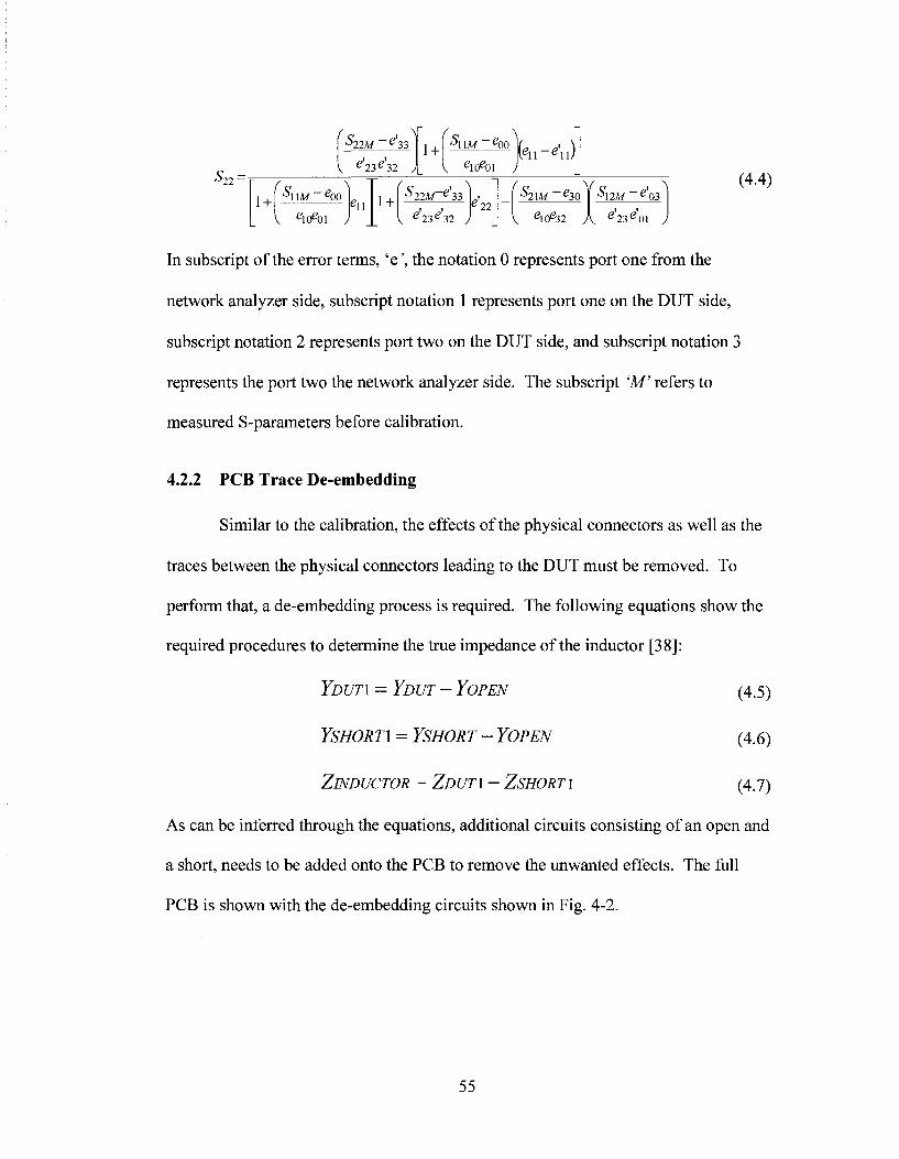
4.2.2 PCB Trace De-embedding
Similar to the calibration, the effects of the physical connectors as well as the
traces between the physical connectors leading to the DUT must be removed. To
perform that, a de-embedding process is required. The following equations show the
required procedures to determine the true impedance of the inductor [38]:
YDUT\ = YDUT - YOPEN (4.5)
YSHORTX = YSHORT - YOPEN (4.6)
ZlNDUCTOR = ZDUTl - ZSHORTX (4.7)
As can be inferred through the equations, additional circuits consisting of an open and
a short, needs to be added onto the PCB to remove the unwanted effects. The full
PCB is shown with the de-embedding circuits shown in Fig. 4-2.
55
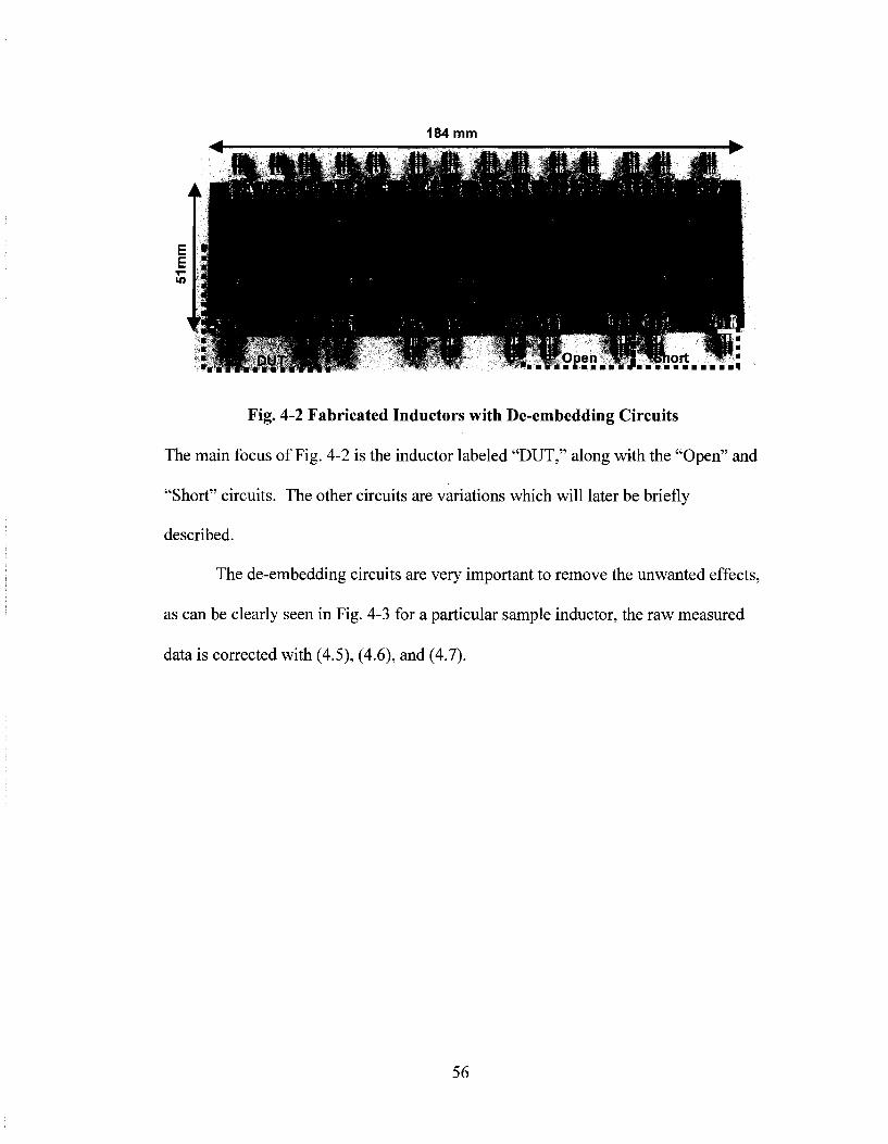
184 mm
Fig. 4-2 Fabricated Inductors with De-embedding Circuits
The main focus of Fig. 4-2 is the inductor labeled "DUT," along with the "Open" and
"Short" circuits. The other circuits are variations which will later be briefly
described.
The de-embedding circuits are very important to remove the unwanted effects,
as can be clearly seen in Fig. 4-3 for a particular sample inductor, the raw measured
data is corrected with (4.5), (4.6), and (4.7).
56
x10" Inductor Parameters
1
E o —I
-1
10 10000
5000 K
0
, measured
, deembed r —
ft : ; - ! • • ! • • ! • •
i J-i ;
: 1 : =
\ : ' :
i
10° 10* ,
measured deembed
I i i
1
i l l ;
....[..:.. P i"
' i '
10' 10c 10M
o
500
0
-500
•1000
—measured -deembed
• r - r - M -
\
rr\-
10' 10° frequency (Hz)
10*
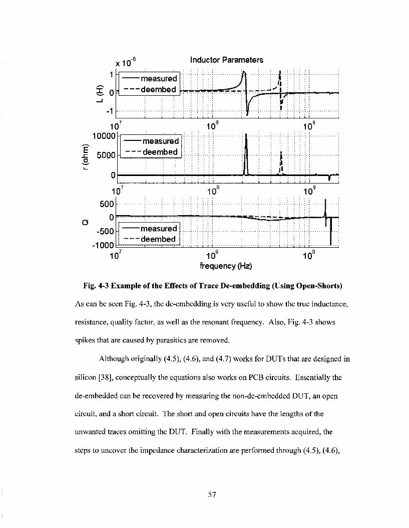
Fig. 4-3 Example of the Effects of Trace De-embedding (Using Open-Shorts)
As can be seen Fig. 4-3, the de-embedding is very useful to show the true inductance,
resistance, quality factor, as well as the resonant frequency. Also, Fig. 4-3 shows
spikes that are caused by parasitics are removed.
Although originally (4.5), (4.6), and (4.7) works for DUTs that are designed in
silicon [38], conceptually the equations also works on PCB circuits. Essentially the
de-embedded can be recovered by measuring the non-de-embedded DUT, an open
circuit, and a short circuit. The short and open circuits have the lengths of the
unwanted traces omitting the DUT. Finally with the measurements acquired, the
steps to uncover the impedance characterization are performed through (4.5), (4.6),
57
and (4.7).
In Fig. 4-2, some interesting conclusions came from designing smaller circuits
with longer feed lines relative to the DUT. First by analyzing (4.5) and (4.6),
intuitively, one can see that if resistance per square between the feed trace and the
DUT are the same, negative impedance may occur if the feed trace length is longer.
Through experimentation, (4.5), (4.6), and (4.7) are accurate when the length of open
and short feed traces are much smaller relative to the length of the DUT trace.
As an experiment, for example, in Fig. 4-2, the accuracy of the smaller
inductors is seen to highly depend on the length of the feed trace to the length of the
DUT trace ratio. The DUTs with N=2.5 and N=l .5 turns for both 30 mil and 60 mil
trace widths were less accurate than the N=3.5, 30 mil and 60 mil circuits. After
further analysis, the DUT of N=3.5 with 60 mil width has higher accuracy than the
N=3.5 with 30 mil width. The reason is because the N=3.5 with 60 mil has an
innately longer DUT trace than the 30 mil DUT trace relative to the same feed traces.
Experimentally, when the feed trace was less than 13.9% of the DUT trace, the results
were much more accurate. The smaller the percentage of feed traces relative to the
DUT traces the better.
The whole process of calibration and de-embedding ensures confidence in the
measurements. From this point on in the next sections, the "measured" results are
regarding the inductors that have been de-embedded.
58
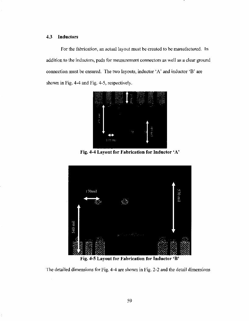
4.3 Inductors
For the fabrication, an actual layout must be created to be manufactured. In
addition to the inductors, pads for measurement connectors as well as a clear ground
connection must be ensured. The two layouts, inductor 'A' and inductor 'B ' are
shown in Fig. 4-4 and Fig. 4-5, respectively.
Fig. 4-4 Layout for Fabrication for Inductor 'A'
Fig. 4-5 Layout for Fabrication for Inductor 'B'
The detailed dimensions for Fig. 4-4 are shown in Fig. 2-2 and the detail dimensions
59
for Fig. 4-5 are shown in Fig. 2-3.
After performing calibration and de-embedding, the measurements for the
inductors are performed. The measured values of DUT from the network analyzer are
converted into MATLAB for comparison purposes.
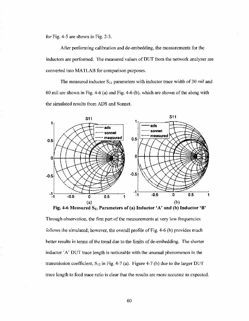
The measured inductor Sn parameters with inductor trace width of 30 mil and
60 mil are shown in Fig. 4-6 (a) and Fig. 4-6 (b), which are shown of the along with
the simulated results from ADS and Sonnet.
(a) (b)
Fig. 4-6 Measured Sn Parameters of (a) Inductor 'A' and (b) Inductor 'B'
Through observation, the first part of the measurements at very low frequencies
follows the simulated; however, the overall profile of Fig. 4-6 (b) provides much
better results in terms of the trend due to the limits of de-embedding. The shorter inductor 'A' DUT trace length is noticeable with the unusual phenomenon in the
transmission coefficient, S12 in Fig. 4-7 (a). Figure 4-7 (b) due to the larger DUT
trace length to feed trace ratio is clear that the results are more accurate as expected.
60
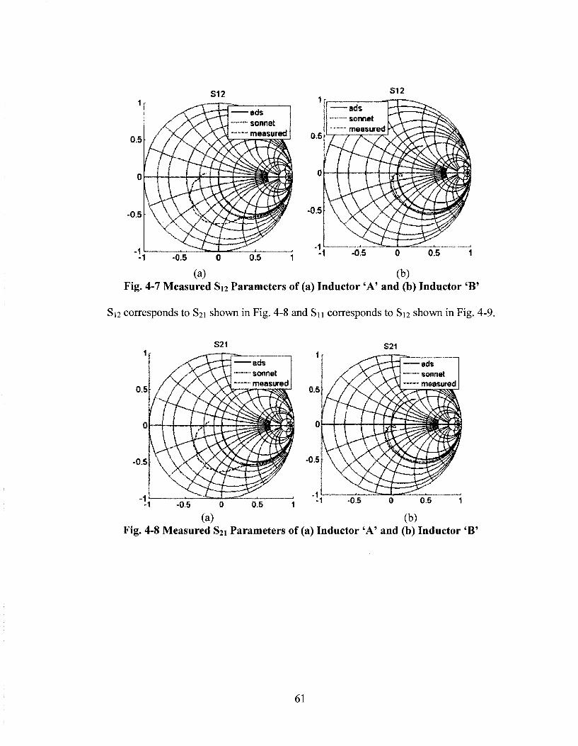
Fig. 4-7 Measured Sn Parameters of (a) Inductor 'A' and (b) Inductor 'B'
S12 corresponds to S21 shown in Fig. 4-8 and Sn corresponds to S12 shown in Fig. 4-9.
Fig. 4-8 Measured S21 Parameters of (a) Inductor 'A' and (b) Inductor 'B'
61
(a) (b)
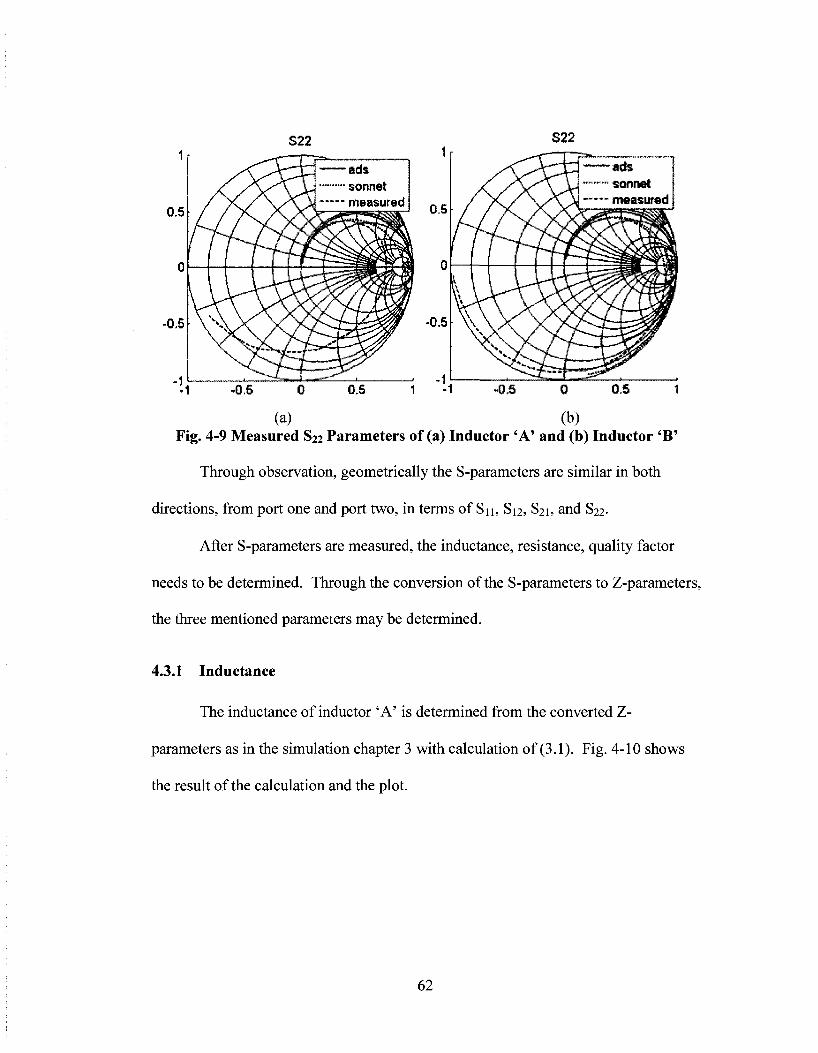
Fig. 4-9 Measured S22 Parameters of (a) Inductor 'A' and (b) Inductor 'B'
Through observation, geometrically the S-parameters are similar in both
directions, from port one and port two, in terms of Sn, S12, S21, and S22.
After S-parameters are measured, the inductance, resistance, quality factor
needs to be determined. Through the conversion of the S-parameters to Z-parameters,
the three mentioned parameters may be determined.
4.3.1 Inductance
The inductance of inductor 'A' is determined from the converted Z-
parameters as in the simulation chapter 3 with calculation of (3.1). Fig. 4-10 shows
the result of the calculation and the plot.
62
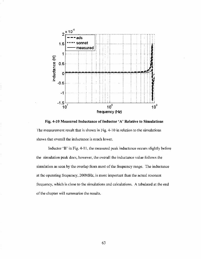
10 frequency (Hz)
Fig. 4-10 Measured Inductance of Inductor 'A' Relative to Simulations
The measurement result that is shown in Fig. 4-10 in relation to the simulations
shows that overall the inductance is much lower.
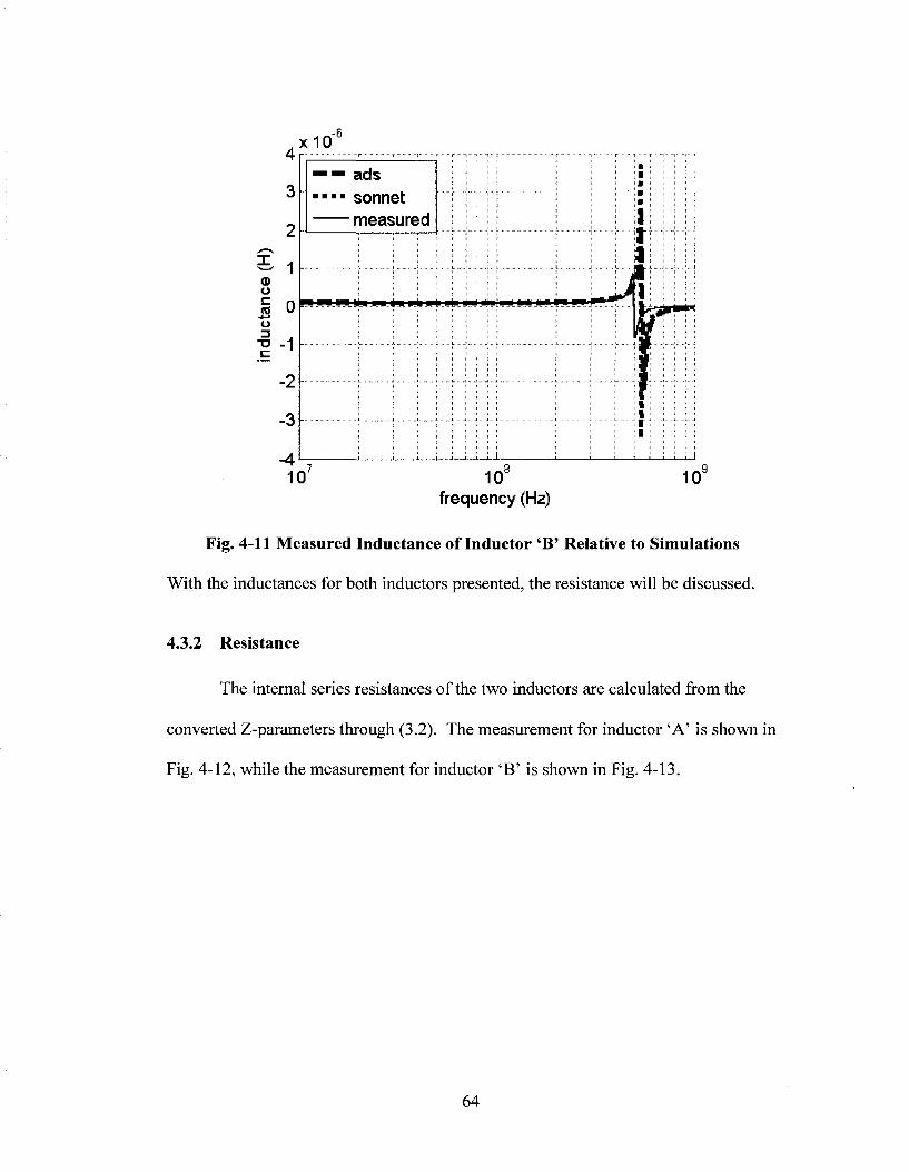
Inductor 'B' in Fig. 4-11, the measured peak inductance occurs slightly before
the simulation peak does, however, the overall the inductance value follows the
simulation as seen by the overlap from most of the frequency range. The inductance
at the operating frequency, 200MHz, is more important than the actual resonant
frequency, which is close to the simulations and calculations. A tabulated at the end
of the chapter will summarize the results.
63
4
3
2
£ 1 (D O « 0 o
i-1
-2
-3
-4
K10"6
— — ads • • • • sonnet
measured
! i,..j._. ' - - | - | | |
i I ; ; ; , , ,
1 f J " " ? " * : J....L..S1
......X-j--^
! I I !
j r
--
• " 1 " T
-i-i
i i 10' 10°
frequency (Hz) 1Cf
Fig. 4-11 Measured Inductance of Inductor 'B' Relative to Simulations
With the inductances for both inductors presented, the resistance will be discussed.
4.3.2 Resistance
The internal series resistances of the two inductors are calculated from the
converted Z-parameters through (3.2). The measurement for inductor 'A' is shown in
Fig. 4-12, while the measurement for inductor 'B' is shown in Fig. 4-13.
64
16000
14000
12000
-g 10000
| 8000
I 6000
4000
2000
0 107
- - - a d s sonne
me as
i i
i i
i I
i
ured
; ;
1
i I i >
i | i i i i
1 10°
frequency (Hz) 10*
Fig. 4-12 Measured Resistance of Inductor 'A' Relative to Simulations
,4 x10
I : i ; ;
T ™ ~r ~r ~r i
10" frequency (Hz)
Fig. 4-13 Measured Resistance of Inductor 'B' Relative to Simulations
65
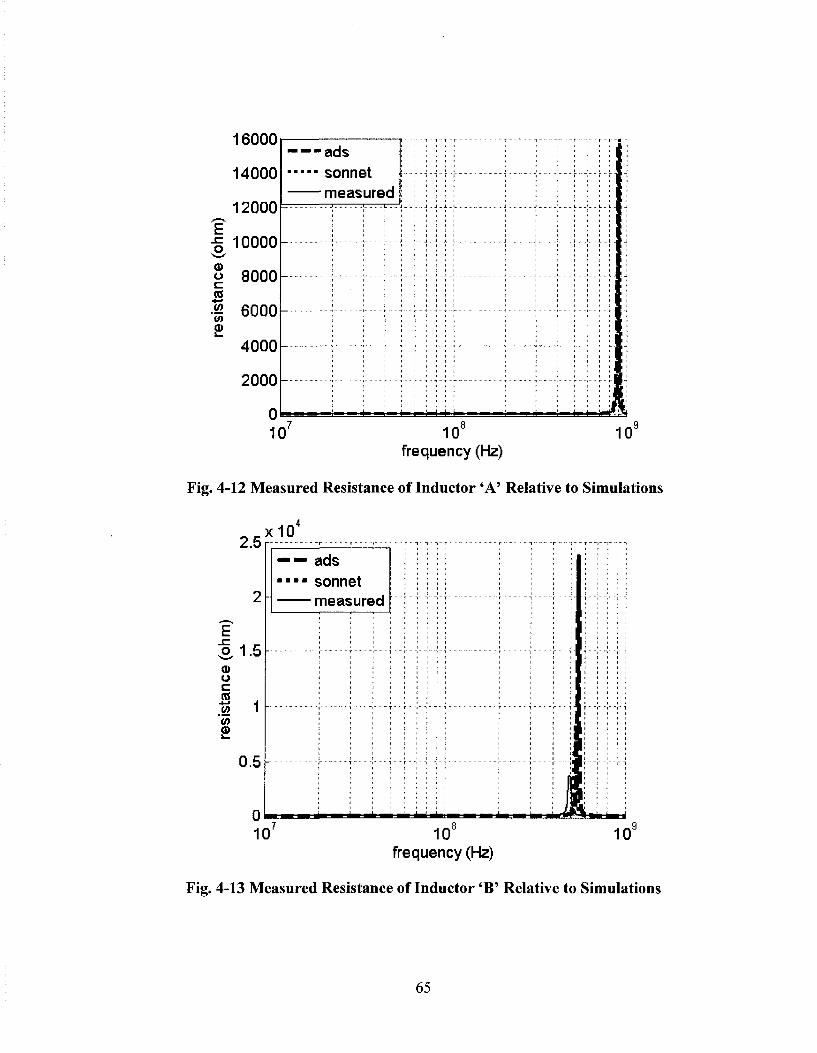
When comparing the two figures, Fig. 4-12 and Fig. 4-13, the first figure, inductor
'A' seems to be following the overall profile. However, in further inspection,
although the peaks are offset, the inductor 'B ' from Fig. 4-13 has also a fairly close
resistance at its operating frequency. The spike of resistance occurs because at the
resonant frequency, the inductor becomes an open circuit. The results of the
inductors will be presented after determining the Q-factor.
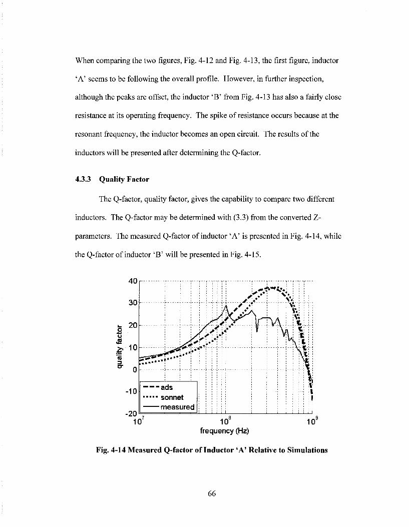
4.3.3 Quality Factor
The Q-factor, quality factor, gives the capability to compare two different
inductors. The Q-factor may be determined with (3.3) from the converted Z-
parameters. The measured Q-factor of inductor 'A' is presented in Fig. 4-14, while
the Q-factor of inductor 'B' will be presented in Fig. 4-15.
10u
frequency (Hz)
Fig. 4-14 Measured Q-factor of Inductor 'A' Relative to Simulations
66
o o
OS
(0 u
60
40
20
0
-20
-40
-60
-80
-100 10
„ C » - ~ .. - I - ~ » „ i . ^ -
~ — ads - • • • • sonnet
measured
, r „ 1 „ 1 -. n . , r . . . „. „ ~. ~ „ „ . - r _ _ . . T ,
j * f • : \ \ k ™ „ J _ J . j . i _ _ _ _ . . . » _ .« _ i V - -*- \
- - - i - - ' i - - i - - i - ! - - - - J - — ; I - - -
I i I : i i ; ;
r .„ _ f .. -,
! • U . . L - |
*~ 1 ~ 1 " 1
» : • • - •
i i 1
10° frequency (Hz)
103
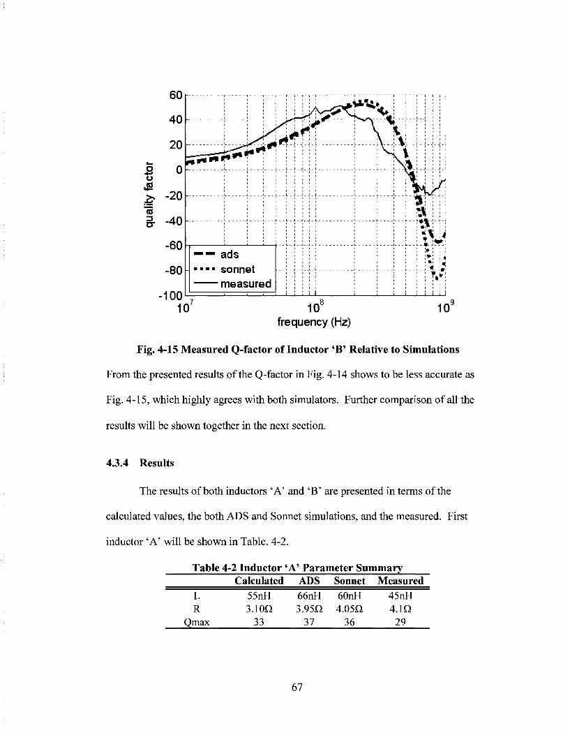
Fig. 4-15 Measured Q-factor of Inductor 'B' Relative to Simulations
From the presented results of the Q-factor in Fig. 4-14 shows to be less accurate as
Fig. 4-15, which highly agrees with both simulators. Further comparison of all the
results will be shown together in the next section.
4.3.4 Results
The results of both inductors 'A' and 'B' are presented in terms of the
calculated values, the both ADS and Sonnet simulations, and the measured. First
inductor 'A' will be shown in Table. 4-2.
Table 4-2 Inductor
L R
Qmax
Calculated 55nH 3.10Q
33
'A' Parameter Summary ADS 66nH 3.95Q.
37
Sonnet 60nH 4.05O
36
Measured 45nH 4AQ. 29
67
The measured Q-factor from inductor 'A' are quite smaller than the calculated and
simulations. The less than expected Q-factor is due to the smaller inductance, which
is related to the feed trace to DUT trace ratio. Better results arise from inductor 'A,'
which has a smaller feed trace to DUT trace ratio, shown in the result summary in
Table 4-3.
Table 4-3 Inductor 'B' Parameter Summary
L R
Qmax
Calculated lOOnH 2.38ft
53
ADS 119nH 3.2ft 52
Sonnet lOlnH 2.85ft
55
Measured 95nH 2.9ft 51
The table of summarized values in Table 4-3 shows that the inductance, resistance,
and Q-factor are all within reasonable agreement to the simulations, calculations, as
well as the design specification.
4.4 Transition from Inductor to Antenna
The inductor began with the design and simulation, which led to the fabrication,
and ended with the measurement. The whole flow and process is described in Fig. 3-
15. The same process is also true with the antenna, where the measurements will be
described after fabrication.
4.5 Antenna
The fabricated GPS antenna of "L-ground plane with lowercase-h configuration
and cornered patch" is shown in Fig. 4-16. The figure shows the front and back of
the fabricated antenna.
68
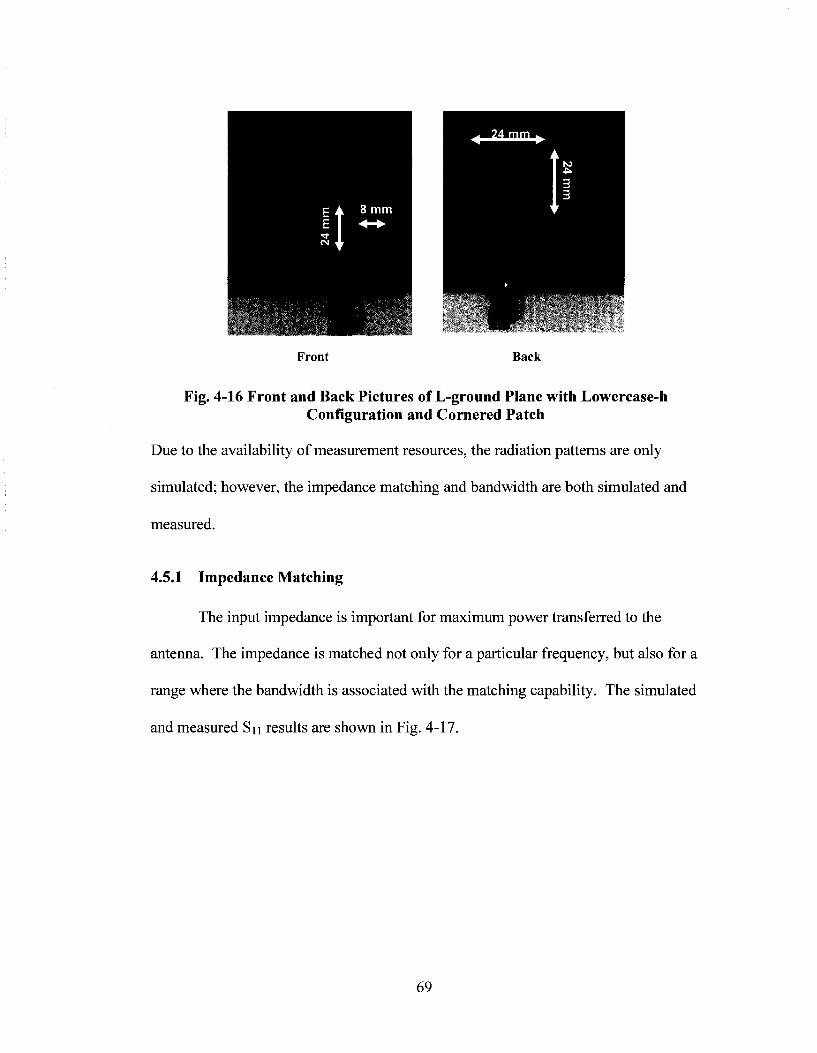
Front Back
Fig. 4-16 Front and Back Pictures of L-ground Plane with Lowercase-h Configuration and Cornered Patch
Due to the availability of measurement resources, the radiation patterns are only
simulated; however, the impedance matching and bandwidth are both simulated and
measured.
4.5.1 Impedance Matching
The input impedance is important for maximum power transferred to the
antenna. The impedance is matched not only for a particular frequency, but also for a
range where the bandwidth is associated with the matching capability. The simulated
and measured Sn results are shown in Fig. 4-17.
69
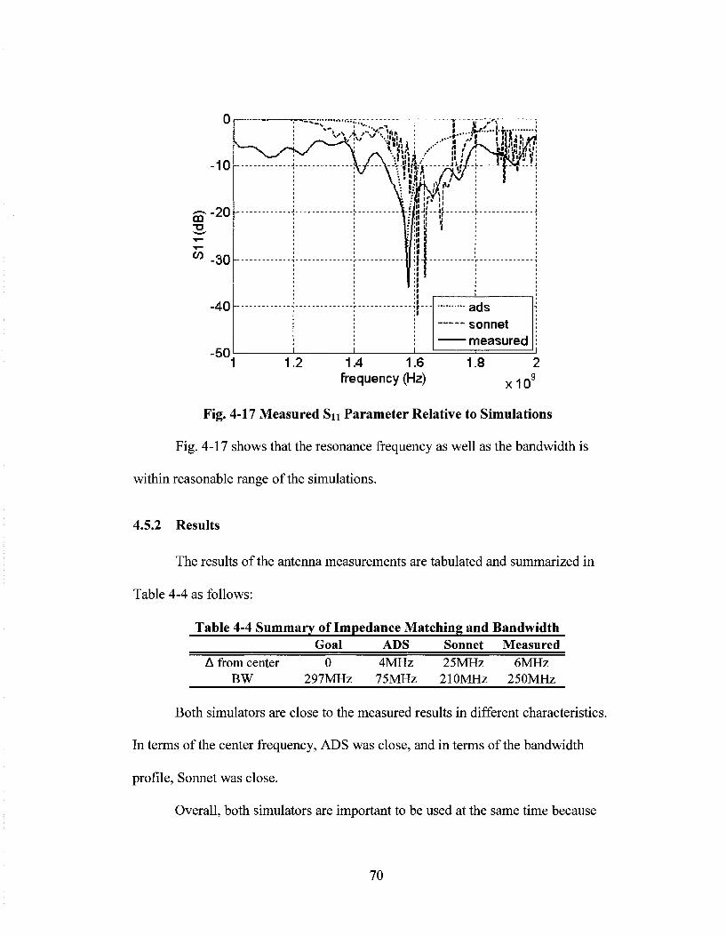
1.4 1.6 frequency (Hz)
Fig. 4-17 Measured Sn Parameter Relative to Simulations
Fig. 4-17 shows that the resonance frequency as well as the bandwidth is
within reasonable range of the simulations.
4.5.2 Results
The results of the antenna measurements are tabulated and summarized in
Table 4-4 as follows:
Table 4-4 Summary of Impedance Matching and Bandwidth Goal ADS Sonnet Measured
A from center 0 4MHz 25MHz 6MHz BW 297MHz 75MHz 210MHz 250MHz
Both simulators are close to the measured results in different characteristics.
In terms of the center frequency, ADS was close, and in terms of the bandwidth
profile, Sonnet was close.
Overall, both simulators are important to be used at the same time because
70
they show different aspects of the device designs, which better predicts the results.
The measured antenna result at 1.5754GHz is |-36d|B, which is sufficient to
the GPS specifications.
4.6 Chapter Summary
This chapter has shown the measurement results for both the inductors and the
antennas, which are reasonable. As can be seen, the second inductor, which has
physically longer component traces relative to the feed trace, has provided more
accurate results, which had helped to characterize the PCB for antenna. With the
complete design flow complete, the thesis will be concluded in the next chapter.
71
5 CONCLUSION
This thesis has shown the full flow starting from designing inductors to
designing antennas through PCB board characterization process. This thesis has fully
explained the background of inductors and antennas as well as the current field work
in the introduction. Next, the theory, analysis, and design chapter has addressed and
organized the essential design parameters. With the design thought process well
defined, simulations are performed in both ADS and Sonnet, which verifies the
expected parameters from the design chapter. To determine the practically, the circuit
boards are fabricated and measured which showed that the design calculations and
simulations were valid.
The presented design flow determined very good results in terms of the larger
inductor and the antenna. The larger lOOnH inductor, earlier denoted as inductor 'B,'
was much better than the 55nH inductor, earlier denoted as inductor 'A,' as
mentioned in chapter 4 section 1.2, due to the ratio of the inductor component's trace
length relative to the feed trace length. Relative to the calculations, ADS simulations,
Sonnet simulations, the measured inductor 'A' Q-factor value varied from as much as
27.57% to down to 10.34%, while the Q-factor for inductor 'B' value varied from as
much as 7.84% to as little as 1.96%. This shows that as long as the inductor
component trace is reasonably long relative to the feed, the results will be accurate.
The accuracy helps to determine the PCB characteristics such as the dielectric
constant, the substrate thickness, and the trace thickness. The results of the antenna
after the modeled PCB characteristics resulted in a final center frequency of
72
1.5814GHz compared to the 1.5754GHz theoretical and 250MHz bandwidth
compared to the desired 297MHz. Considering even small manufacturing variations
create drastic antenna characteristic results, the measured results are good. Also, the
help of the initial inductor design processes increased accuracy in terms of expected
variations from optimizing the simulators.
The significance of this thesis is that it shows a student or one who may be
interested in antenna design a flow using any available PCB fabrication process.
Through the proposed method used is described with inductors essential to radio
frequency and microwave that began the design flow. The presented design flow is a
valuable contribution to academia.
This project may be extended in the future. First, analyzing the components
in an anechoic would be very helpful in further analysis. Secondly, an extension
would be to determine the upper limitations of the correlations between the inductor
and antenna in terms of frequencies and size. Lastly, higher inductance planar
inductors with various cores may be experimentally performed.
73
References
[I] H. D. Young and R. A. Freedman, University Physics with Modern Physics, San Francisco: Addison Wesley Longman, 2000.
[2] J. Sevick, Transmission Line Transformers, Newington: American Radio Relay League, 1987.
[3] S. Sridharan, W. Grande, and P.R. Mukund, "High Q embedded inductors in silicon for RF applications," IEEE International ASIC/SOC Conference, pp. 346-349, Sept. 2002
[4] H. Ronkainen, H. Kattelus, E. Tarvainen, T. Ruhissari, M. Andersson, and P. Kuivalainen, "IC Compatible planar inductors on silicon, " IEE Proceedings-Circuits, Devices and Systems, vol. 144, no. 1, pp. 29-35, Feb. 1997.
[5] E. Ragonese, T. Biondi, A. Scuderi, and G. Palmisano, "A lumped scalable physics-based model for silicon spiral inductors" The 10th IEEE International Symposium on Electron Devices for Microwave and Optoelectronic Applications, pp. 119-124, Nov. 2002.
[6] T.-P. Wang, H. Wang, "High-Q Micromachined Inductors for 10-to-30GHz RFIC Applications on Low Resistivity Si-Substrate" 36th European Microwave Conference, pp. 56-59, Sept. 2006.
[7] J.R. Long and M.A. Copeland, "The modeling, characterization, and design of monolithic inductors for silicon RF IC's," IEEE Journal of Solid-State Circuits, vol. 32, no. 3, pp. 357-369, Mar. 1997.
[8] S. Staff, "Printed Inductors in RF Consumer Applications," IEEE Trans, on Consum. Electron., vol. 47, no. 3, pp. 426-435, Aug 2001.
[9] C.P. Yue and S.S. Wong, "Physical modeling of spiral inductors on silicon," IEEE Transactions on Electron Devices, vol. 47. no. 3, pp. 560-568, Mar. 2000.
[10] J. L. Sinclair, How Radio Signals work, Australia: McGraw-Hill Book Company Australia Pty Limited, 1997.
[II] R. Garg, P. Bhartia, I. Bahl, and A. Ittipiboon, Microstrip Antenna Design Handbook, Norwood: Artech House, Inc., 2001.
74
[12] Stanford Report, "GPS inventor inducted into hall of fame," http://news-service.stanford.edu/news/2004/february 18/parkinson-218.html, Feb. 18, 2004.
[13] International information programs - Current Issues, "United States Updates Global Positioning System Technology," Feb. 3, 2006. [Online]. Available: http://usinfo.state.gov/gi/Archive/2006/Feb/06-791119.html
[14] Global Positioning System Standard Positioning Service Standard, Oct. 2001. [Online]. Available: http://www.navcen.uscg.gov/gps/geninfo/ 2001 SPSPerformanceStandardFINAL.pdf
[15] M.K. Alsliety and D.N. Aloi, "A Study of Ground-Plane-Level and Vehicle-Level Radiation Patterns of GPS Antenna in Telematics Applications," IEEE Antennas and Wireless Propag. Lett., vol. 6, pp. 130-133, 2007.
[16] R. Li, B. Pan, J. Laskar, and M.M. Tentzeris, "A Compact Broadband Planar Antenna for GPS, DCS-1800, IMT-2000, and WLAN Applications," IEEE Antennas and Wireless Propag. Lett., vol. 6, pp.25-27, 2007.
[17] Y. Zhou, C.-C. Chen, and J.L. Volakis, "Dual Band Proximity-Fed Stacked Patch Antenna for Tri-Band GPS Applications," IEEE Trans. Antennas Propag., vol. 55, no. 1, pp. 220-223, Jan. 2007.
[18] R. A. Serway and R. J. Beichner, Physics for Scientists and Engineers, 5l ed. Orlando: Saunders College Publishing, 2000.
[19] C.K. Alexander and M. N. O. Sadiku, Fundamental of Electric Circuits, 2nd
ed. New York: McGraw-Hill, 2004.
[20] H. M. Greenhouse, "Design of Planar Rectangular Microelectronic Inductors," IEEE Trans, on Parts, hybrids, and Packaging, vol. 10, no. 2, pp. 101-109, Jun. 1974.
[21] W.B. Kuhn, A. Elshabini-Riad, and F.W. Stephenson, "Centre-tapped spiral inductors for monolithic bandpass filters," IEE Electron. Lett., vol. 31, no. 8, pp. 625-626, Apr. 1995
[22] C. R. Paul, "Transmission Lines and Signal Integrity" Introduction to Electromagnetic Compatibility, 2nd ed. New Jersey: John Wiley & Sons, Inc., 2006, ch. 4, sec. 5, pp. 274-275.
[23] D. M. Pozar, Microwave Engineering, 3rd ed. New Jersey: John Wiley & Sons, Inc., 2005.
75
[24] I. Sinclair, "Inductors and inductive components," Passive Components for Circuit Design, Woburn: Newnes, 2001, ch. 5, pp. 134-135.
[25] Q. Zhu, K. Fu, and T.-Z. Liang, "Analysis of planar inverted-F antenna using equivalent models," 2005 IEEE Antennas and Propagation Society International Symposium, vol. 3A, pp. 142-145, Jul. 2005.
[26] G. Qasim, W. Zhao, and J. Zhang, "Inverted F-antenna for mobile communication," AMPC 2005 Microwave Conference Proceedings, vol. 5, pp. 4, Dec. 2005.
[27] V. F. Fusco, Foundations of Antenna Theory and Techniques, Essex: Pearson Education Limited, 2005.
[28] Advanced Design System Documentation, Agilent Technologies, Santa Clara, CA, 2004A, ch. 9 pp. 1-12.
[29] D. K. Cheng, "Plane Electromagnetic Waves," Fundamentals of Engineering Electromagnetics, New Jersey: Prentice-Hall, Inc., 1993, ch. 7, sec. 2, pp.272 -287.
[30] R. Bancroft, "Rectangular Microstrip Antennas," Microstrip and Printed Antenna Design, Atlanta: Noble Publishing Corporation, 2004, ch. 2, sec. 5, pp. 37-48.
[31] G. Kumar and K.P. Ray, "An Introduction to Microstrip Antennas" Broadband Microstrip Antennas, Norwood: Artech House, Inc., 2003, ch. 1, sec.5, pp.11-18.
[32] Z. N. Chen and M. Y. W. Chia, Broadband Planar Antennas, West Sussex: John Wiley & Sons Ltd., 2006.
[33] M. Drakaki, A. Hatzopoulos, and A. Siskos, "CMOS Inductor Performance Estimation using Z- and S-parameters," IEEE International Symposium on Circuits and Systems, 2007, pp. 2256-2259, May 2007.
[34] J. R. James and P.S. Hall, Handbook of Microstrip Antennas, vol. 1. London: Peter Peregrinus Ltd., 1989.
[35] M.D. DuFault and A.K. Sharma, "A novel calibration verification procedure for millimeter-wave measurements," IEEE MTT-S International Microwave Symposium Digest, vol. 3, pp. 1391-1394, Jun. 1996.
76
[36] D.C. DeGroot, K.L. Reed, and J.A. Jargon, "Equivalent Circuit Models for Coaxial OSLT Standards," 54th ARFTG Conference Digest-Spring, vol. 36, pp. 1-13, vol. 36, Dec. 2000.
[37] D. Rytting. (1998, Sept.). Network Analyzer Error Models and Calibration Methods. Hewlett-Packard Company. [Online White Paper]. Available: http://cpd.ogi.edu/IEEE-MTT-ED/Network%20Analyzer%20error%20Models%20and%20Calibration%20 Methods.pdf
[38] D.M. Jamal and T.A. Fieldly, CMOS RF Modeling, Characterization and Applications, Singapore: World Scientific Publishing, 2002.
77