
Design Example Report - Power · Design Example Report ... Capacitor C12 is the main supply for the...
48
Power Integrations 5245 Hellyer Avenue, San Jose, CA 95138 USA. Tel: +1 408 414 9200 Fax: +1 408 414 9201 www.powerint.com Design Example Report Title Broad TRIAC Dimmer Capability 6.9 W LED Driver Using LinkSwitch TM -PH LNK404EG Specification 185 VAC – 264 VAC (50 Hz) Input; 26.5 V TYP , 260 mA Output Application LED Driver Author Applications Engineering Department Document Number DER-269 Date March 7, 2011 Revision 1.0 Summary and Features Superior performance and end user experience TRIAC dimmer compatible Compatibility includes low cost leading edge and high power rating types No output flicker >1000:1 dimming range (dependant on dimmer model) Clean monotonic start-up – no output blinking Fast start-up (<100 ms) – no perceptible delay Consistent dimming performance unit to unit Highly energy efficient ≥78% at 230 VAC Frequency jitter for smaller, lower cost EMI filter components Integrated protection and reliability features Output open circuit / output short-circuit protected with auto-recovery Line input overvoltage shutdown extends voltage withstand during line faults. Auto-recovering thermal shutdown with large hysteresis protects both components and printed circuit board No damage during brown-out or brown-in conditions PATENT INFORMATION The products and applications illustrated herein (including transformer construction and circuits external to the products) may be covered by one or more U.S. and foreign patents, or potentially by pending U.S. and foreign patent applications assigned to Power Integrations. A complete list of Power Integrations' patents may be found at www.powerint.com. Power Integrations grants its customers a license under certain patent rights as set forth at <http://www.powerint.com/ip.htm>.
Transcript of Design Example Report - Power · Design Example Report ... Capacitor C12 is the main supply for the...

Power Integrations
5245 Hellyer Avenue, San Jose, CA 95138 USA. Tel: +1 408 414 9200 Fax: +1 408 414 9201
www.powerint.com
Design Example Report
Title Broad TRIAC Dimmer Capability 6.9 W LED Driver Using LinkSwitchTM-PH LNK404EG
Specification 185 VAC – 264 VAC (50 Hz) Input; 26.5 VTYP, 260 mA Output
Application LED Driver
Author Applications Engineering Department
Document Number
DER-269
Date March 7, 2011
Revision 1.0 Summary and Features Superior performance and end user experience
TRIAC dimmer compatible Compatibility includes low cost leading edge and high power rating types No output flicker >1000:1 dimming range (dependant on dimmer model)
Clean monotonic start-up – no output blinking Fast start-up (<100 ms) – no perceptible delay Consistent dimming performance unit to unit
Highly energy efficient ≥78% at 230 VAC
Frequency jitter for smaller, lower cost EMI filter components Integrated protection and reliability features
Output open circuit / output short-circuit protected with auto-recovery Line input overvoltage shutdown extends voltage withstand during line faults. Auto-recovering thermal shutdown with large hysteresis protects both components
and printed circuit board No damage during brown-out or brown-in conditions
PATENT INFORMATION The products and applications illustrated herein (including transformer construction and circuits external to the products) may be covered by one or more U.S. and foreign patents, or potentially by pending U.S. and foreign patent applications assigned to Power Integrations. A complete list of Power Integrations' patents may be found at www.powerint.com. Power Integrations grants its customers a license under certain patent rights as set forth at <http://www.powerint.com/ip.htm>.

DER-269 6.9 W A19 LED Driver Using LNK404EG 07-Mar-11
Page 2 of 48
Power Integrations, Inc. Tel: +1 408 414 9200 Fax: +1 408 414 9201 www.powerint.com
Table of Contents 1 Introduction ................................................................................................................. 4 2 Prototype Provisions to Meet Safety Standards ......................................................... 6 3 Power Supply Specification ........................................................................................ 7 4 Schematic ................................................................................................................... 8 5 Circuit Description ...................................................................................................... 9
5.1 Input Filtering ....................................................................................................... 9 5.2 LinkSwitch-PH Primary ........................................................................................ 9 5.3 Bias and Output Rectification .............................................................................. 9 5.4 TRIAC Phase Dimming Control ........................................................................... 9 5.5 TRIAC Active Load ............................................................................................ 10
6 PCB Layout .............................................................................................................. 11 7 Bill of Materials ......................................................................................................... 14
7.1 Main Board ........................................................................................................ 14 7.2 Daughter Board ................................................................................................. 15
8 Transformer Specification ......................................................................................... 16 8.1 Electrical Diagram ............................................................................................. 16 8.2 Electrical Specifications ..................................................................................... 16 8.3 Materials ............................................................................................................ 16 8.4 Transformer Build Diagram ............................................................................... 17 8.5 Transformer Construction .................................................................................. 17
9 Transformer Design Spreadsheet ............................................................................. 18 10 Performance Data ................................................................................................. 21
10.1 Efficiency ........................................................................................................... 22 10.2 Line and Load .................................................................................................... 23 10.3 Power Factor ..................................................................................................... 24 10.4 Total Harmonic Distortion .................................................................................. 25
11 Thermal Performance ........................................................................................... 26 11.1 Non-Dimming Measurements ............................................................................ 26 11.2 Dimming Measurements .................................................................................... 28
12 Harmonic Data ...................................................................................................... 29 12.1 8 LED Load ~23 V Output ................................................................................. 29 12.2 9 LED Load ~27 V Output ................................................................................. 31 12.3 10 LED Load ~29 V Output ............................................................................... 33
13 Waveforms ............................................................................................................ 35 13.1 Drain Voltage and Current ................................................................................. 35 13.2 Output Diode Peak Inverse Voltage .................................................................. 35 13.3 Input Line Voltage and Current (No TRIAC Dimmer Connected) ...................... 36 13.4 Input Voltage and Input Current Waveforms (During Dimming) ........................ 36 13.5 Output Voltage and Ripple Current ................................................................... 37 13.6 Drain Voltage and Current Start-up Profile ........................................................ 38 13.7 Output Current and Drain Voltage at Shorted Output ........................................ 39 13.8 Open Load Output Voltage ................................................................................ 39
14 Dimmer Compatibility ............................................................................................ 40 14.1 Korean Dimmer: New Touch, 120 W ................................................................. 40

07-Mar-11 DER-269 6.9 W A19 LED Driver Using LNK404EG
Page 3 of 48
Power Integrations Tel: +1 408 414 9200 Fax: +1 408 414 9201
www.powerint.com
14.2 German Dimmer: REV300, 300 W ..................................................................... 41 14.3 German Dimmer: BUSCH 2250, 600 W ............................................................ 42 14.4 German Dimmer: MERTEN 572499, 400 W ...................................................... 43 14.5 German Dimmer: BERKER 2875, 600 W .......................................................... 44
15 Conducted EMI ..................................................................................................... 45 15.1 Conducted EMI Test Set-up .............................................................................. 46
16 Revision History .................................................................................................... 47 Important Note: Although this board is designed to satisfy safety isolation requirements, the engineering prototype has not been agency approved. Therefore, all testing should be performed using an isolation transformer to provide the AC input to the prototype board.

DER-269 6.9 W A19 LED Driver Using LNK404EG 07-Mar-11
Page 4 of 48
Power Integrations, Inc. Tel: +1 408 414 9200 Fax: +1 408 414 9201 www.powerint.com
1 Introduction The document describes a high power-factor corrected dimmable LED driver designed to drive 26.5 V LED at 260 mA from an input voltage range of 185 VAC to 264 VAC. The LED driver utilizes the LNK404EG from Power Integrations. LinkSwitch-PH ICs allow the implementation of cost effective and low component count LED drivers which both meet power factor and harmonics limits but also offer enhanced end user experience. This includes ultra-wide dimming range, flicker free operation (even with low cost with AC line TRIAC dimmers) and fast, clean turn on. The topology used is an isolated flyback operating in continuous conduction mode. Output current regulation is sensed entirely from the primary side eliminating the need for secondary side feedback components. No external current sensing is required on the primary side either as this is performed inside the IC further reducing components and losses. The internal controller adjusts the MOSFET duty cycle to maintain a sinusoidal input current and therefore high power factor and low harmonic currents. The LNK404EG also provides a sophisticated range of protection features including auto-restart for open control loop and output short-circuit conditions. Line overvoltage provides extended line fault and surge withstand, output overvoltage protects the supply should the load be disconnect and accurate hysteretic thermal shutdown ensures safe average PCB temperatures under all conditions. In any LED luminaries the driver determines many of the performance attributes experienced by the end customer (user) including startup time, dimming, flicker and unit to unit consistency. For this design a focus was given to compatibility with as wider range of dimmers including high power (1000 W) rated dimmers at 230 VAC. This document contains the LED driver specification, schematic, PCB diagram, bill of materials, transformer documentation and typical performance characteristics.

07-Mar-11 DER-269 6.9 W A19 LED Driver Using LNK404EG
Page 5 of 48
Power Integrations Tel: +1 408 414 9200 Fax: +1 408 414 9201
www.powerint.com
Figure 1 – Populated Circuit Board Photograph (Top View).
PCB Outline Designed to Fit Inside A19 Enclosure.
Figure 2 – Populated Circuit Board Photograph Single Sided PCB (Bottom View).

DER-269 6.9 W A19 LED Driver Using LNK404EG 07-Mar-11
Page 6 of 48
Power Integrations, Inc. Tel: +1 408 414 9200 Fax: +1 408 414 9201 www.powerint.com
2 Prototype Provisions to Meet Safety Standards
1. Output capacitor C4 located on the bottom side of the board is in closed proximity to the primary components. If not enough spacing is met during the final assembly, this capacitor should be wrapped by 3 layers of safety approved tape, i.e. 3M polyester film or equivalent.
2. The transformer (T1) core is considered primary due to the proximity of the primary windings to the core. The nearest secondary components are the output terminals. Core wrapping must be employed to provide adequate safety spacing and isulation.
3. The body of Y capacitor C17 must also be wrapped with safety insulation tape or equivalent form of reinforced insulation if its distance from the transformer cannot be maintained.
2 (T1) 3 (C17)
1 (C4)

07-Mar-11 DER-269 6.9 W A19 LED Driver Using LNK404EG
Page 7 of 48
Power Integrations Tel: +1 408 414 9200 Fax: +1 408 414 9201
www.powerint.com
3 Power Supply Specification The table below represents the minimum acceptable performance of the design. Actual performance is listed in the results section.
Description Symbol Min Typ Max Units Comment
Input Voltage VIN 185 230 264 VAC 2 Wire – no P.E.
Frequency fLINE 50 Hz
Output
Output Voltage VOUT 22 26.5 29 V
Output Current IOUT 0.260 A VOUT = 22, VIN = 230 / 60Hz VAC, 25°C
Total Output Power
Continuous Output Power POUT 6.9 W
Efficiency
Full Load 78 % Measured at POUT 25 oC
Environmental
Conducted EMI Meets CISPR 15B / EN55015B
Safety Designed to meet IEC950 / UL1950 Class II
Ring Wave (100 kHz) Differential Mode (L1-L2) Common mode (L1/L2-PE)
Power Factor 0.9 Measured at VOUT(TYP), IOUT(TYP) and 230 VAC
Harmonics EN 61000-3-2 Class C
Ambient Temperature TAMB 25 oC Free convection, sea level

DER-269 6.9 W A19 LED Driver Using LNK404EG 07-Mar-11
Page 8 of 48
Power Integrations, Inc. Tel: +1 408 414 9200 Fax: +1 408 414 9201 www.powerint.com
4 Schematic
Figure 3 – LinkSwitch-PH LED DRIVER Schematic (TRIAC Active Bleeder Circuit in Dotted Line).

07-Mar-11 DER-269 6.9 W A19 LED Driver Using LNK404EG
Page 9 of 48
Power Integrations Tel: +1 408 414 9200 Fax: +1 408 414 9201
www.powerint.com
5 Circuit Description The LinkSwitch-PH device is a controller and integrated 725 V MOSFET intended for use in LED driver applications. The LinkSwitch-PH is configured for use in a single-stage continuous conduction mode flyback topology and provides a primary side regulated constant current output while maintaining high power factor from the AC input.
5.1 Input Filtering Fuse F1 provide protection from catastrophic failure of any of the primary side components. Bridge BR1 rectifies the AC line voltage. Inductor L1-L4, R2, R3, R8, R9, and C10, provide EMI filtering together with C17 Y capacitor. Small bulk capacitor C10 is required for a low impedance path for the primary switching current. A low value of capacitance is necessary to maintain a power factor of greater than 0.8.
5.2 LinkSwitch-PH Primary Diode D6 and C8 detect the peak AC line voltage. This voltage is converted to a current into the V pin via R4, R7 and R13. Diode D7 and R13 provide additional V pin current during deep dimming to inhibit the undervoltage threshold of the IC. The presence of D7 disables the undervoltage feature of the IC without affecting the overvoltage protection. The V pin current and the FEEDBACK (FB) pin current are used internally to control the average output LED current. Resistor R19 was set to 24.9 k to achieve tight line and load regulation. Diode D1, R26, R28, R25 and C16 clamp the drain voltage to a safe level from the leakage inductance voltage spike. Diode D5 is necessary to prevent reverse current from flowing through the LinkSwitch-PH device.
5.3 Bias and Output Rectification Diode D3, C6, R5, and R18 create the primary bias supply. This voltage created from the transformer bias winding supplies bias current into the BYPASS (BP) pin through D4 and R10. Capacitor C12 is the main supply for the LinkSwitch-PH, which is charged to ~6 V at start-up from an internal high-voltage current source tied to the device DRAIN pin. A current proportional to the output voltage from the primary bias winding is fed into the FB pin through R15. Diode D2 rectifies the secondary winding while capacitor C4 filters the output. VR3, C15, R23, and Q2 provide an open load overvoltage protection function. This protects output capacitors C4 from excessive voltage should the load be disconnected.
5.4 TRIAC Phase Dimming Control
Resistors R16 act as a damping network preventing the input current from ringing negative when the TRIAC dimmer turns on and thereby creating flicker. SCR Q3, R11, R12 and C13 shorts R16 after the transient has subsided and thus saves unnecessary power loss on R16. Capacitors C9, C11 and R10 and R17 provides the latching current for the TRIAC once conducting and also helps further dampen ringing.

DER-269 6.9 W A19 LED Driver Using LNK404EG 07-Mar-11
Page 10 of 48
Power Integrations, Inc. Tel: +1 408 414 9200 Fax: +1 408 414 9201 www.powerint.com
5.5 TRIAC Active Load The TRIAC active load formed by Q4, R29 and the entire sub circuit on the small daughter board is used to satisfy compatibility with high power TRIACs (>600 W). This network draws a constant current of ~40 mA once activated. Resistors R31-R33 sense the average input voltage and switches on the active load Q4 for conduction angles ~<90 degrees and thus provides the holding current required by the TRIAC. The holding current drawn by the active load is set by VR4 and parallel combination of R20 and R17. Transistor Q5 turns-off the active load during full phase (and ~>90 degrees) conduction and thus eliminate its associated losses during non dimming conditions. Resistors R34, R35 and Q7 provide hysteresis on the average sensing network. Voltage regulator VR5 and VBE of Q5 and Q6 sets the turn-on and turn-off threshold of the TRIAC active load. Power from this circuit is drawn from the bias winding supply.

07-Mar-11 DER-269 6.9 W A19 LED Driver Using LNK404EG
Page 11 of 48
Power Integrations Tel: +1 408 414 9200 Fax: +1 408 414 9201
www.powerint.com
6 PCB Layout
Figure 4 – Printed Circuit Layout, Top Side (Designed to Fit Inside A19 Lamp Form Factor).
DER-269 6.9 W A19 LED Driver Using LNK404EG 07-Mar-11
Page 12 of 48
Power Integrations, Inc. Tel: +1 408 414 9200 Fax: +1 408 414 9201 www.powerint.com
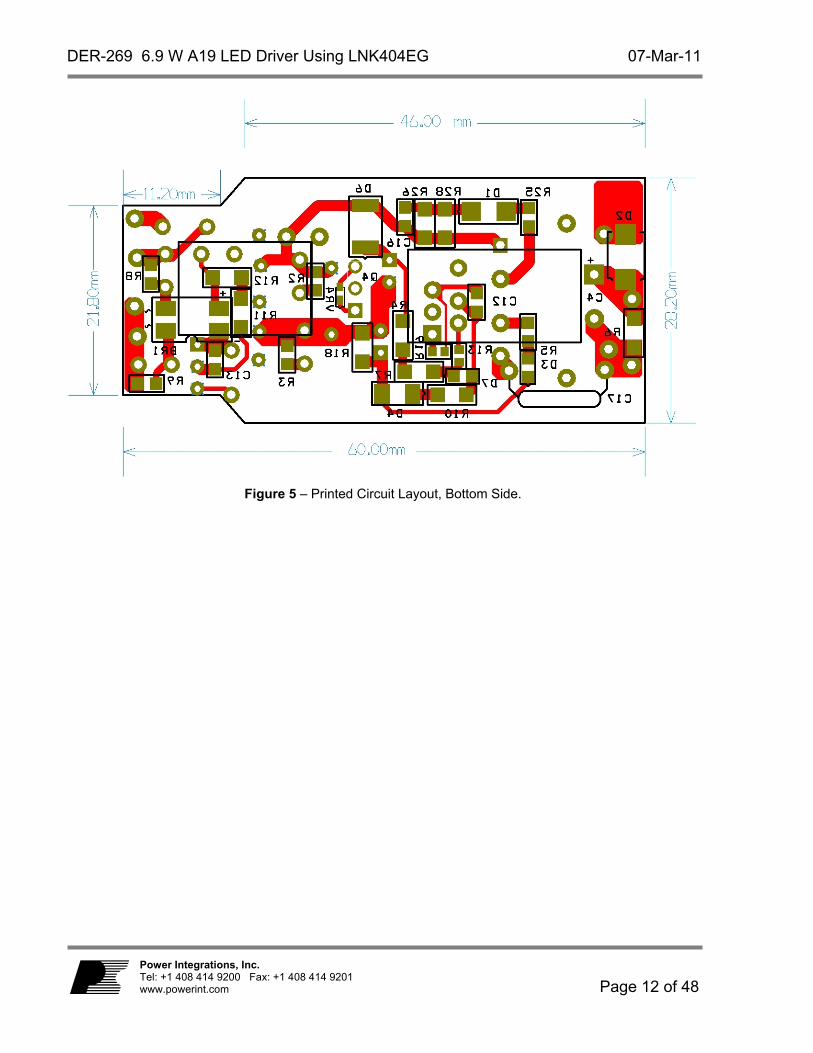
Figure 5 – Printed Circuit Layout, Bottom Side.

07-Mar-11 DER-269 6.9 W A19 LED Driver Using LNK404EG
Page 13 of 48
Power Integrations Tel: +1 408 414 9200 Fax: +1 408 414 9201
www.powerint.com
Figure 6 – TRIAC Active Load Daughter Board PCB Layout, Top.
Figure 7 – TRIAC Active Load Daughter Board PCB Layout, Top.

DER-269 6.9 W A19 LED Driver Using LNK404EG 07-Mar-11
Page 14 of 48
Power Integrations, Inc. Tel: +1 408 414 9200 Fax: +1 408 414 9201 www.powerint.com
7 Bill of Materials
7.1 Main Board
Item Qty Ref Des
Description Mfg Part Number Mfg
1 1 BR1 600 V, 0.5 A, Bridge Rectifier, SMD, MBS-1, 4-SOIC MB6S-TP Micro
Commercial
2 1 C4 270 F, 50 V, Electrolytic, Very Low ESR, 30 m, (10 x 20)
EKZE500ELL271MJ20S Nippon Chemi-
Con
3 1 C6 22 F, 50 V, Electrolytic, Low ESR, 900 m, (5 x 11.5)
ELXZ500ELL220MEB5D Nippon Chemi-
Con
4 1 C8 1 F, 400 V, Electrolytic, (6.3 x 11) EKMG401ELL1R0MF11D United Chemi-
Con
5 2 C9 C11 100 nF, 500 V, Ceramic, X7R, 1812 VJ1812Y104KXEAT Vishay
6 1 C10 33 nF, 400 V, Film ECQ-E4333KF Panasonic
7 1 C12 10 F, 16 V, Ceramic, X5R, 0805 GRM21BR61C106KE15L Murata
8 1 C13 22 nF, 50 V, Ceramic, X7R, 0805 ECJ-2VB1H223K Panasonic
9 1 C15 100 nF 25 V, Ceramic, X7R, 0603 ECJ-1VB1E104K Panasonic
10 1 C16 1 nF, 1000 V, Ceramic, X7R, 0805 C0805C102KDRACTU Kemet
11 1 C17 1 nF, Ceramic, Y1 ECK-ANA102MB Panasonic
12 1 D1 600 V, 1 A, Fast Recovery, 250 ns, SMA RS1J-13-F Diodes, Inc
13 1 D2 150 V, 1 A, Ultrafast Recovery, 35 ns, SMB Case MURS115T3 On Semi
14 2 D3 D7 250 V, 0.2 A, Fast Switching, 50 ns, SOD-323 BAV21WS-7-F Diodes, Inc
15 1 D4 75 V, 0.15 A, Fast Switching, 4 ns, MELF LL4148-13 Diodes, Inc
16 1 D5 DIODE ULTRA FAST, SW, 200 V, 1 A, SMA US1D-13-F Diodes, Inc
17 1 D6 1000 V, 1 A, Rectifier, Glass Passivated, DO-213AA (MELF)
DL4007-13-F Diodes, Inc
18 1 F1 3.15 A, 250 V, Slow, RST 507-1181 Belfuse
19 4 L1 L2 L3 L4 4.7 mH, 90 mA, 20 , RF Inductor B82144A2475J Epcos
20 1 Q2 NPN, Small Signal BJT, 40 V, 0.2 A, SOT-23 MMBT3904LT1G On Semi
21 1 Q3 SCR, 400 V, 1.25 A, TO-92 FS0202DA Fagor
22 1 Q4 500 V, 4.4 A, 1200 m. N-Channel, TO-220F STP5NK50ZFP ST
23 2 R2 R3 4.7 k, 5%, 1/8 W, Thick Film, 0805 ERJ-6GEYJ472V Panasonic
24 1 R4 2.4 M, 5%, 1/4 W, Thick Film, 1206 ERJ-8GEYJ245V Panasonic
25 1 R5 22 , 5%, 1/8 W, Thick Film, 0805 ERJ-6GEYJ220V Panasonic
26 3 R6 R10
R18 10 k, 5%, 1/4 W, Thick Film, 1206 ERJ-8GEYJ103V Panasonic
27 1 R7 1.50 M, 1%, 1/4 W, Thick Film, 1206 ERJ-8ENF1504V Panasonic
28 2 R8 R9 10 k, 5%, 1/8 W, Thick Film, 0805 ERJ-6GEYJ103V Panasonic
29 2 R11 R12 750 k, 5%, 1/4 W, Thick Film, 1206 ERJ-8GEYJ754V Panasonic
30 1 R13 100 k, 1%, 1/16 W, Thick Film, 0603 ERJ-3EKF1003V Panasonic
31 2 R14 510 , 5%, 2 W, Metal Oxide RSF200JB-510R Yageo
32 1 R15 178 k, 1%, 1/16 W, Thick Film, 0603 ERJ-3EKF1783V Panasonic
33 1 R16 270 , 5%, 1 W, Metal Oxide RSF100JB-270R Yageo
34 1 R19 49.9 k, 1%, 1/16 W, Thick Film, 0603 ERJ-3EKF4992V Panasonic
35 1 R23 750 , 5%, 1/10 W, Thick Film, 0603 ERJ-3GEYJ751V Panasonic
36 1 R25 100 , 5%, 1/8 W, Thick Film, 0805 ERJ-6GEYJ101V Panasonic

07-Mar-11 DER-269 6.9 W A19 LED Driver Using LNK404EG
Page 15 of 48
Power Integrations Tel: +1 408 414 9200 Fax: +1 408 414 9201
www.powerint.com
37 2 R26 R28 200 k, 5%, 1/4 W, Thick Film, 1206 ERJ-8GEYJ204V Panasonic
38 1 R29 1 k, 5%, 2 W, Metal Oxide RSF200JB-1K0 Yageo
39 1 RV1 275 V, 23 J, 7 mm, RADIAL V275LA4P Littlefuse
40 1 U1 LinkSwitch-PH, eSIP LNK404EG Power
Integrations
41 1 U2 Bobbin, RM6_S/I, Vertical, 4 pins w 2 pin clip CPV-RM6S/I-1S-8PD Ferroxcube
42 1 VR3 39 V, 5%, 150 mW, SSMINI-2 MAZS39000L Panasonic
43 1 VR4 8.2 V, 5%, 150 mW, SSMINI-2 MAZS0820ML Panasonic
7.2 Daughter Board Item Qty Ref Des Description Mfg Part Number Mfg
45 2 C14 C19 10 nF 50 V, Ceramic, X7R, 0603 ECJ-1VB1H103K Panasonic
46 1 C18 10 F, 16 V, Ceramic, X5R, 0805 GRM21BR61C106KE15L Murata
47 1 C20 220 nF, 25 V, Ceramic, X7R, 0805 ECJ-2YB1E224K Panasonic
48 3 Q5 Q6
Q7 NPN, Small Signal BJT, 40 V, 0.2 A, SOT-23 MMBT3904LT1G On Semi
49 2 R17 R20 200 , 5%, 1/4 W, Thick Film, 1206 ERJ-8GEYJ201V Panasonic
50 4 R21 R22 R32 R33 750 k, 5%, 1/4 W, Thick Film, 1206 ERJ-8GEYJ754V Panasonic
51 1 R24 10 k, 5%, 1/10 W, Thick Film, 0603 ERJ-3GEYJ103V Panasonic
52 1 R30 10 k, 5%, 1/4 W, Thick Film, 1206 ERJ-8GEYJ103V Panasonic
53 1 R31 30 k, 5%, 1/10 W, Thick Film, 0603 ERJ-3GEYJ303V Panasonic
54 1 R34 470 k, 5%, 1/8 W, Thick Film, 0805 ERJ-6GEYJ474V Panasonic
55 1 R35 4.7 k, 5%, 1/10 W, Thick Film, 0603 ERJ-3GEYJ472V Panasonic
56 1 R36 1 k, 5%, 1/10 W, Thick Film, 0603 ERJ-3GEYJ102V Panasonic
57 1 VR4 8.2 V, 5%, 150 mW, SSMINI-2 MAZS0820ML Panasonic
58 1 VR5 3 V, 5%, 500 mW, DO-213AA (MELF) ZMM5225B-7 Diodes Inc

DER-269 6.9 W A19 LED Driver Using LNK404EG 07-Mar-11
Page 16 of 48
Power Integrations, Inc. Tel: +1 408 414 9200 Fax: +1 408 414 9201 www.powerint.com
8 Transformer Specification
8.1 Electrical Diagram
Figure 8 – Transformer Electrical Diagram.
8.2 Electrical Specifications Electrical Strength 1 second, 60 Hz, from pins 1-4 and leads FL1-FL2. 3000 VAC
Primary Inductance Pins 1-2, all other windings open, measured at 100 kHz, 0.4 VRMS
3.3 mH, ±5%
Resonant Frequency Pins 1-2, all other windings open 800 kHz (Min.) Primary Leakage Inductance
Pins 1-2, with leads FL1-FL2 shorted, measured at 100kHz, 0.4 VRMS.
30 H (Max.)
8.3 Materials Item Description [1] Core: RM6 [2] Bobbin: RM6-Vertical, 8 pins (4/4). AllStar P/N: CPV-RM6 5/1-1S. [3] Magnet wire: #37 AWG. [4] Magnet wire: #27 AWG Triple Insulated Wire. [5] Tape: 3M 1298 Polyester Film, 6.5mm wide, 2.0 mils thick or equivalent. [6] Core clip: Ferrox Cube #: FXC-0102718, CLI-RM6/I. [7] Varnish: Dolph BC-359 or equivalent.

07-Mar-11 DER-269 6.9 W A19 LED Driver Using LNK404EG
Page 17 of 48
Power Integrations Tel: +1 408 414 9200 Fax: +1 408 414 9201
www.powerint.com
8.4 Transformer Build Diagram
Figure 9 – Transformer Build Diagram.
8.5 Transformer Construction Bobbin
Preparation Remove all secondary pins and flange of bobbin item [2]. Cut all primary side pins.
Winding Preparation
Place the bobbin on the mandrel with the pin side is on the left side. Winding direction is clockwise direction.
WD1 1st Primary
Take ~12 ft of wire item [3], start at pin 2, and wind 44 turns from left to right. Place 1 layer of tape item [5], then continue winding 44 turns from right to left and leave the remain of this wire on the mandrel for the WD4 2nd primary winding.
Insulation Place 1 layer of tape item [5]. WD2
Secondary Use wire item [4], starting as FL1 (floating lead), wind 22 turns in 2 layers from left to right then from right to left and end at FL2. (The last turn might be on 3rd layer).
Insulation Place 1 layer of tape item [5]. WD3 Bias
Start at pin 3, wind 27 turns of wire item [3] from left to right, spread the wire evenly. At the last turn bring the wire back to the left and terminate at pin 4.
Insulation Place 1 layer of tape item [5]. WD4
2nd Primary Use the remain wire from WD1 1st primary, continue winding 40 turns from left to right, at the last turn bring the wire back to the left and terminate at pin 1.
Insulation Place 2 layers of tape item [5]. Final Assembly Grind, assemble, and secure core halves with clips item [6]. Vanish item [7].

DER-269 6.9 W A19 LED Driver Using LNK404EG 07-Mar-11
Page 18 of 48
Power Integrations, Inc. Tel: +1 408 414 9200 Fax: +1 408 414 9201 www.powerint.com
9 Transformer Design Spreadsheet ACDC_LinkSwitch-PH_061010; Rev.1.1; Copyright Power Integrations 2010 INPUT INFO OUTPUT UNIT
LinkSwitch-PH_061010: Flyback Transformer Design Spreadsheet
ENTER APPLICATION VARIABLES
Dimming required NO NO Select 'YES' option if dimming is required. Otherwise select 'NO'.
VACMIN 187 187 V Minimum AC Input Voltage VACMAX 264 264 V Maximum AC input voltage fL 50 Hz AC Mains Frequency
VO 26.40 V Typical output voltage of LED string at full load
VO_MAX 29.04 V Maximum expected LED string Voltage. VO_MIN 23.76 V Minimum expected LED string Voltage. V_OVP 31.94 V Over-voltage protection setpoint IO 0.26 Typical full load LED current PO 6.9 W Output Power n 0.8 Estimated efficiency of operation VB 32 32 V Bias Voltage ENTER LinkSwitch-PH VARIABLES LinkSwitch-PH LNK404 Universal 115 Doubled/230V
Chosen Device LNK404 Power
Out 15.5W 15.5W
Current Limit Mode RED RED Select "RED" for reduced Current Limit mode or "FULL" for Full current limit mode
ILIMITMIN 0.81 A Minimum current limit ILIMITMAX 0.92 A Maximum current limit fS 66000 Hz Switching Frequency fSmin 62000 Hz Minimum Switching Frequency fSmax 70000 Hz Maximum Switching Frequency IV 78.4 uA V pin current RV 4.00 4 M-ohms Upper V pin resistor RV2 1.402 M-ohms Lower V pin resistor IFB 110.00 110.0 uA FB pin current (85 uA < IFB < 210 uA) RFB1 263.6 k-ohms FB pin resistor
VDS 10 V LinkSwitch-PH on-state Drain to Source Voltage
VD 0.50 V Output Winding Diode Forward Voltage Drop (0.5 V for Schottky and 0.8 V for PN diode)
VDB 0.70 V Bias Winding Diode Forward Voltage Drop
Key Design Parameters KP 1.31 Warning 1.31 !!! Warning. KP is too high. Decrease KP LP 3315 uH Primary Inductance VOR 156.51 156.51 V Reflected Output Voltage. Expected IO (average) 0.27 A Expected Average Output Current
KP_VACMAX 1.35 !!! Info. PF at high line may be less than 0.9. Decrease KP for higher PF
TON_MIN 2.22 us Minimum on time at maximum AC input voltage
PCLAMP 0.05 W Estimated dissipation in primary clamp ENTER TRANSFORMER CORE/CONSTRUCTION VARIABLES Core Type RM6S/I RM6S/I Bobbin RM6S/I_BOBBIN P/N: * AE 0.37 cm^2 Core Effective Cross Sectional Area LE 2.92 cm Core Effective Path Length AL 2150 nH/T^2 Ungapped Core Effective Inductance BW 6.4 mm Bobbin Physical Winding Width
M 0 mm Safety Margin Width (Half the Primary to Secondary Creepage Distance)

07-Mar-11 DER-269 6.9 W A19 LED Driver Using LNK404EG
Page 19 of 48
Power Integrations Tel: +1 408 414 9200 Fax: +1 408 414 9201
www.powerint.com
L 3 Number of Primary Layers NS 22 22 Number of Secondary Turns DC INPUT VOLTAGE PARAMETERS VMIN 264 V Peak input voltage at VACMIN VMAX 373 V Peak input voltage at VACMAX CURRENT WAVEFORM SHAPE PARAMETERS DMAX 0.32 Minimum duty cycle at peak of VACMIN IAVG 0.04 A Average Primary Current
IP 0.35 A Peak Primary Current (calculated at minimum input voltage VACMIN)
IRMS 0.09 A Primary RMS Current (calculated at minimum input voltage VACMIN)
TRANSFORMER PRIMARY DESIGN PARAMETERS LP 3315 uH Primary Inductance NP 128 Primary Winding Number of Turns NB 27 Bias Winding Number of Turns ALG 202 nH/T^2 Gapped Core Effective Inductance
BM 2437 Gauss Maximum Flux Density at PO, VMIN (BM<3100)
BP 2949 Gauss Peak Flux Density (BP<3700)
BAC 1219 Gauss AC Flux Density for Core Loss Curves (0.5 X Peak to Peak)
ur 1350 Relative Permeability of Ungapped Core LG 0.21 mm Gap Length (Lg > 0.1 mm) BWE 19.2 mm Effective Bobbin Width
OD 0.15 mm Maximum Primary Wire Diameter including insulation
INS 0.03 mm Estimated Total Insulation Thickness (= 2 * film thickness)
DIA 0.12 mm Bare conductor diameter
AWG 37 AWG Primary Wire Gauge (Rounded to next smaller standard AWG value)
CM 20 Cmils Bare conductor effective area in circular mils
CMA 228 Cmils/Amp Primary Winding Current Capacity (200 < CMA < 600)
LP_TOL 10 Tolerance of primary inductance TRANSFORMER SECONDARY DESIGN PARAMETERS (SINGLE OUTPUT EQUIVALENT) Lumped parameters ISP 2.03 A Peak Secondary Current ISRMS 0.74 A Secondary RMS Current IRIPPLE 0.70 A Output Capacitor RMS Ripple Current
CMS 149 Cmils Secondary Bare Conductor minimum circular mils
AWGS 28 AWG Secondary Wire Gauge (Rounded up to next larger standard AWG value)
DIAS 0.32 mm Secondary Minimum Bare Conductor Diameter
ODS 0.29 mm Secondary Maximum Outside Diameter for Triple Insulated Wire
VOLTAGE STRESS PARAMETERS
VDRAIN 686 V Estimated Maximum Drain Voltage assuming maximum LED string voltage (Includes Effect of Leakage Inductance)
PIVS 96 V Output Rectifier Maximum Peak Inverse Voltage (calculated at VOVP, excludes leakage inductance spike)
PIVB 117 V Bias Rectifier Maximum Peak Inverse Voltage (calculated at VOVP, excludes leakage inductance spike)
FINE TUNING (Enter measured values from prototype) V pin Resistor Fine Tuning RV1 4.00 M-ohms Upper V Pin Resistor Value RV2 1.40 M-ohms Lower V Pin Resistor Value VAC1 115.0 V Test Input Voltage Condition1 VAC2 230.0 V Test Input Voltage Condition2

DER-269 6.9 W A19 LED Driver Using LNK404EG 07-Mar-11
Page 20 of 48
Power Integrations, Inc. Tel: +1 408 414 9200 Fax: +1 408 414 9201 www.powerint.com
IO_VAC1 0.26 A Measured Output Current at VAC1 IO_VAC2 0.26 A Measured Output Current at VAC2 RV1 (new) 4.00 M-ohms New RV1 RV2 (new) 1.40 M-ohms New RV2
V_OV 325.6 V Typical AC input voltage at which OV shutdown will be triggered
V_UV 72.4 V Typical AC input voltage beyond which power supply can startup
FB pin resistor Fine Tuning RFB1 264 k-ohms Upper FB Pin Resistor Value RFB2 1E+012 k-ohms Lower FB Pin Resistor Value VB1 28.8 V Test Bias Voltage Condition1 VB2 35.2 V Test Bias Voltage Condition2 IO1 0.26 A Measured Output Current at Vb1 IO2 0.26 A Measured Output Current at Vb2 RFB1 (new) 263.6 k-ohms New RFB1 RFB2(new) 1.00E+12 k-ohms New RFB2
Note: The KP is higher than normal to keep the circuit operating in discontinuous mode (DCM) at high line for improved efficiency. The design does pass harmonic and power factor specifications.

07-Mar-11 DER-269 6.9 W A19 LED Driver Using LNK404EG
Page 21 of 48
Power Integrations Tel: +1 408 414 9200 Fax: +1 408 414 9201
www.powerint.com
10 Performance Data All measurements performed at room temperature. Yokogawa Power Meter Model: WT210 was used to measure accurately the true output power and input power of the unit.
Input Input Measurement Load Measurement VAC
(VRMS) V
(VRMS) I
(ARMS) P
(W) PF %ATHD V
(VDC) I
(ADC) PO (W)
Efficiency(%)
185 184.8 0.046 8.006 0.939 25.98 23.64 0.268 6.40 79.9
198 197.8 0.044 8.046 0.930 27.14 23.64 0.269 6.43 79.9
220 219.9 0.040 8.051 0.913 28.56 23.63 0.268 6.40 79.5
230 229.8 0.039 8.035 0.905 29.15 23.62 0.267 6.37 79.3
253 252.9 0.036 8.018 0.887 30.57 23.61 0.266 6.33 78.9
264 263.8 0.035 8.003 0.878 31.38 23.60 0.265 6.31 78.8
Table 1 – 8 LED String (~23 V) Load Test Data.
Input Input Measurement Load Measurement VAC
(VRMS) V
(VRMS) I
(ARMS) P
(W) PF %ATHD V
(VDC) I
(ADC) PO (W)
Efficiency(%)
185 184.9 0.052 9.045 0.946 25.45 26.76 0.266 7.19 79.5
198 197.9 0.049 9.073 0.938 26.71 26.74 0.267 7.21 79.5
220 220.0 0.045 9.074 0.923 28.14 26.72 0.267 7.19 79.2
230 229.9 0.043 9.047 0.916 28.66 26.69 0.266 7.15 79.0
253 253.0 0.040 9.004 0.900 29.85 26.66 0.263 7.08 78.6
264 264.0 0.038 8.974 0.892 30.52 26.63 0.262 7.04 78.4
Table 2 – 9 LED String (~26 V) Load Test Data.
Input Input Measurement Load Measurement VAC
(VRMS) V
(VRMS) I
(ARMS) P
(W) PF %ATHD V
(VDC) I
(ADC) PO (W)
Efficiency(%)
185 184.9 0.057 9.949 0.952 25.01 29.57 0.264 7.88 79.2
198 197.9 0.053 9.983 0.944 26.23 29.55 0.266 7.91 79.2
220 220.0 0.049 9.988 0.931 27.91 29.53 0.265 7.90 79.1
230 229.9 0.047 9.967 0.925 28.26 29.51 0.264 7.86 78.9
253 253.0 0.043 9.909 0.910 29.22 29.48 0.261 7.77 78.4
264 264.0 0.041 9.869 0.903 29.93 29.46 0.260 7.72 78.2
Table 3 – 10 LED String (~29 V) Load Test Data.

DER-269 6.9 W A19 LED Driver Using LNK404EG 07-Mar-11
Page 22 of 48
Power Integrations, Inc. Tel: +1 408 414 9200 Fax: +1 408 414 9201 www.powerint.com
10.1 Efficiency
78.0
78.2
78.4
78.6
78.8
79.0
79.2
79.4
79.6
79.8
80.0
180 190 200 210 220 230 240 250 260 270
Input Voltage (VAC)
Eff
icie
ncy
(%
)
8 LED9 LED10 LED
Figure 10 – Efficiency vs. Input Voltage, Room Temperature.

07-Mar-11 DER-269 6.9 W A19 LED Driver Using LNK404EG
Page 23 of 48
Power Integrations Tel: +1 408 414 9200 Fax: +1 408 414 9201
www.powerint.com
10.2 Line and Load
0.259
0.261
0.263
0.265
0.267
0.269
0.271
180 190 200 210 220 230 240 250 260 270
Input Voltage (VAC)
Ou
tpu
t C
urr
ent
(A)
8 LED9 LED10 LED
Figure 11 – Line and Load Regulation.

DER-269 6.9 W A19 LED Driver Using LNK404EG 07-Mar-11
Page 24 of 48
Power Integrations, Inc. Tel: +1 408 414 9200 Fax: +1 408 414 9201 www.powerint.com
10.3 Power Factor
0.87
0.88
0.89
0.90
0.91
0.92
0.93
0.94
0.95
0.96
180 190 200 210 220 230 240 250 260 270Input Voltage (VAC)
Po
wer
Fac
tor
8 LED9 LED10 LED
Figure 12 – Power Factor vs. Line and Load.

07-Mar-11 DER-269 6.9 W A19 LED Driver Using LNK404EG
Page 25 of 48
Power Integrations Tel: +1 408 414 9200 Fax: +1 408 414 9201
www.powerint.com
10.4 Total Harmonic Distortion
24
25
26
27
28
29
30
31
32
180 190 200 210 220 230 240 250 260 270
Input Voltage (VAC)
A-T
HD
(%
)8 LED9 LED10 LED
Figure 13 – THD vs. Line and Load.

DER-269 6.9 W A19 LED Driver Using LNK404EG 07-Mar-11
Page 26 of 48
Power Integrations, Inc. Tel: +1 408 414 9200 Fax: +1 408 414 9201 www.powerint.com
11 Thermal Performance The following infrared measurements were taken at room temperature after soaking the unit for 1 hour in the conditions stated below. Note: During dimming condition, the bleeder and active load components will have a high increase in temperature. The assumption is that during the final assembly, the whole board will be potted (encapsulated) inside the lamp enclosure. Junction temperature of active load MOSFET and bleeder resistors must be measured once potted to ensure that maximum component temperature ratings are not exceeded. The heat sink of Q4 can still be increased to further improve thermal performance.
11.1 Non-Dimming Measurements
Figure 14 – Top Side Measurements, 230 VAC, 50 Hz, Non-Dimming.
Figure 15 – LNK404EG, 230 VAC, 50 Hz, Non-Dimming.

07-Mar-11 DER-269 6.9 W A19 LED Driver Using LNK404EG
Page 27 of 48
Power Integrations Tel: +1 408 414 9200 Fax: +1 408 414 9201
www.powerint.com
Figure 16 – Bottom Side Measurements, 230 VAC, 50 Hz, Non-Dimming.
Figure 17 – Output Rectifier D2, 230 VAC, 50 Hz, Non-Dimming.

DER-269 6.9 W A19 LED Driver Using LNK404EG 07-Mar-11
Page 28 of 48
Power Integrations, Inc. Tel: +1 408 414 9200 Fax: +1 408 414 9201 www.powerint.com
11.2 Dimming Measurements
Figure 18 – 230 VAC, 50 Hz, 90º Phase (R29).
Figure 19 – 230 VAC, 50 Hz, 90º Phase (Q4 Heat Sink).

07-Mar-11 DER-269 6.9 W A19 LED Driver Using LNK404EG
Page 29 of 48
Power Integrations Tel: +1 408 414 9200 Fax: +1 408 414 9201
www.powerint.com
12 Harmonic Data The design passes Class C requirement.
12.1 8 LED Load ~23 V Output
n Measured
(mA)
Base I Harmonics
(mA/W)
230 V Limit (mA)
Remarks
1 37.110
3 8.740 3.40000 27.435 Pass
5 4.420 1.90000 15.331 Pass
7 2.770 1.00000 8.069 Pass
9 2.160 0.50000 4.035 Pass
11 1.730 0.35000 2.824 Pass
13 1.410 0.29615 2.390 Pass
15 1.200 0.25667 2.071 Pass
17 0.910 0.22647 1.827 Pass
19 0.780 0.20263 1.635 Pass
21 0.470 0.18333 1.479 Pass
23 0.400 0.16739 1.351 Pass
25 0.160 0.15400 1.243 Pass
27 0.130 0.14259 1.151 Pass
29 0.070 0.13276 1.071 Pass
31 0.100 0.12419 1.002 Pass
33 0.140 0.11667 0.941 Pass
35 0.190 0.11000 0.888 Pass
37 0.190 0.10405 0.840 Pass
39 0.240 0.09872 0.797 Pass
Table 4 – 8 LED Load Input Harmonics.

DER-269 6.9 W A19 LED Driver Using LNK404EG 07-Mar-11
Page 30 of 48
Power Integrations, Inc. Tel: +1 408 414 9200 Fax: +1 408 414 9201 www.powerint.com
0
5
10
15
20
25
30
3 5 7 9 11 13 15 17 19 21 23 25 27 29 31 33 35 37 39
Harmonic Order
Har
mo
nic
Cu
rren
t (m
A)
Class C Limit8 LED Load
Figure 20 – Input Harmonics, 230 VAC, 50 Hz, 8 LED String.

07-Mar-11 DER-269 6.9 W A19 LED Driver Using LNK404EG
Page 31 of 48
Power Integrations Tel: +1 408 414 9200 Fax: +1 408 414 9201
www.powerint.com
12.2 9 LED Load ~27 V Output
n Measured
(mA)
Base I Harmonics
(mA/W)
230 V Limit (mA)
Remarks
1 41.320
3 9.770 3.40000 30.906 Pass
5 4.750 1.90000 17.271 Pass
7 2.860 1.00000 9.090 Pass
9 2.140 0.50000 4.545 Pass
11 1.700 0.35000 3.182 Pass
13 1.370 0.29615 2.692 Pass
15 1.220 0.25667 2.333 Pass
17 0.850 0.22647 2.059 Pass
19 0.740 0.20263 1.842 Pass
21 0.460 0.18333 1.667 Pass
23 0.390 0.16739 1.522 Pass
25 0.170 0.15400 1.400 Pass
27 0.140 0.14259 1.296 Pass
29 0.150 0.13276 1.207 Pass
31 0.190 0.12419 1.129 Pass
33 0.240 0.11667 1.061 Pass
35 0.270 0.11000 1.000 Pass
37 0.280 0.10405 0.946 Pass
39 0.320 0.09872 0.897 Pass
Table 5 – 9 LED Load Input Harmonics.

DER-269 6.9 W A19 LED Driver Using LNK404EG 07-Mar-11
Page 32 of 48
Power Integrations, Inc. Tel: +1 408 414 9200 Fax: +1 408 414 9201 www.powerint.com
0
5
10
15
20
25
30
35
3 5 7 9 11 13 15 17 19 21 23 25 27 29 31 33 35 37 39
Harmonic Order
Har
mo
nic
Cu
rren
t (m
A)
Class C Limit9 LED Load
Figure 21 – Input Harmonics, 230 VAC, 50 Hz, 9 LED String.

07-Mar-11 DER-269 6.9 W A19 LED Driver Using LNK404EG
Page 33 of 48
Power Integrations Tel: +1 408 414 9200 Fax: +1 408 414 9201
www.powerint.com
12.3 10 LED Load ~29 V Output
n Measured
(mA)
Base I Harmonics
(mA/W)
230 V Limit (mA)
Remarks
1 45.140
3 10.680 3.40000 33.993 Pass
5 5.110 1.90000 18.996 Pass
7 2.980 1.00000 9.998 Pass
9 2.200 0.50000 4.999 Pass
11 1.660 0.35000 3.499 Pass
13 1.330 0.29615 2.961 Pass
15 1.150 0.25667 2.566 Pass
17 0.960 0.22647 2.264 Pass
19 0.850 0.20263 2.026 Pass
21 0.530 0.18333 1.833 Pass
23 0.480 0.16739 1.674 Pass
25 0.230 0.15400 1.540 Pass
27 0.210 0.14259 1.426 Pass
29 0.100 0.13276 1.327 Pass
31 0.150 0.12419 1.242 Pass
33 0.210 0.11667 1.166 Pass
35 0.270 0.11000 1.100 Pass
37 0.280 0.10405 1.040 Pass
39 0.280 0.09872 0.987 Pass
Table 6 – 10 LED Load Input Harmonics.

DER-269 6.9 W A19 LED Driver Using LNK404EG 07-Mar-11
Page 34 of 48
Power Integrations, Inc. Tel: +1 408 414 9200 Fax: +1 408 414 9201 www.powerint.com
0
5
10
15
20
25
30
35
40
3 5 7 9 11 13 15 17 19 21 23 25 27 29 31 33 35 37 39
Harmonic Order
Har
mo
nic
Cu
rren
t (m
A)
Class C Limit10 LED Load
Figure 22 – Input Harmonics, 230 VAC, 50 Hz, 10 LED String.

07-Mar-11 DER-269 6.9 W A19 LED Driver Using LNK404EG
Page 35 of 48
Power Integrations Tel: +1 408 414 9200 Fax: +1 408 414 9201
www.powerint.com
13 Waveforms
13.1 Drain Voltage and Current
Figure 23 – 185 VAC, Full Load. Upper: IDRAIN, 0.1 A / div. Lower: VDRAIN, 100 V, 10 s / div.
Figure 24 – 265 VAC, Full Load. Upper: IDRAIN, 0.1 A / div. Lower: VDRAIN, 100 V / div., 10 s / div.
13.2 Output Diode Peak Inverse Voltage
Figure 25 – 265 VAC, Full Load.
VPIV, 20 V, 2 ms / div.

DER-269 6.9 W A19 LED Driver Using LNK404EG 07-Mar-11
Page 36 of 48
Power Integrations, Inc. Tel: +1 408 414 9200 Fax: +1 408 414 9201 www.powerint.com
13.3 Input Line Voltage and Current (No TRIAC Dimmer Connected)
Figure 26 – 185 VAC, Full Load. Upper: IIN, 0.05 A / div. Lower: VIN, 100 V, 10 ms / div.
Figure 27 – 265 VAC, Full Load. Upper: IIN, 0.05 A / div. Lower: VIN, 100 V / div., 10 ms / div.
13.4 Input Voltage and Input Current Waveforms (During Dimming)
Figure 28 – 230 VAC, Full Phase. Upper: IIN, 0.05 A / div., 5 ms / div. Lower: VIN, 100 V / div.
Figure 29 – 230 VAC, 90° Phase. Upper: IIN, 0.05 A / div., 5 ms / div. Lower: VIN, 100 V / div.

07-Mar-11 DER-269 6.9 W A19 LED Driver Using LNK404EG
Page 37 of 48
Power Integrations Tel: +1 408 414 9200 Fax: +1 408 414 9201
www.powerint.com
Figure 30 – 230 VAC, 45° Phase. Lower: VIN, 100 V / div. Upper: IIN, 0.05 A / div., 5 ms / div.
Figure 31 – 230 VAC, 18° Phase. Lower: VIN, 100 V / div. Upper: IIN, 0.05 A / div., 5 ms / div.
13.5 Output Voltage and Ripple Current
Figure 32 – 185 VAC, Full Load. Lower: VOUT 5 V, 5 ms / div. Upper: IRIPPLE, 0.1 A / div.
Figure 33 – 265 VAC, Full Load. Lower: VOUT 5 V, 5 ms / div. Upper: IRIPPLE, 0.1 A / div.

DER-269 6.9 W A19 LED Driver Using LNK404EG 07-Mar-11
Page 38 of 48
Power Integrations, Inc. Tel: +1 408 414 9200 Fax: +1 408 414 9201 www.powerint.com
13.6 Drain Voltage and Current Start-up Profile
`
Figure 34 – 185 VAC, Full Load. Lower: VDRAIN, 100 V, 20 ms / div. Upper: IDRAIN, 0.1 A / div.
Figure 35 – 265 VAC, Full Load. Lower: VDRAIN, 100 V, 20 ms / div. Upper: IRIPPLE, 0.1 A / div.

07-Mar-11 DER-269 6.9 W A19 LED Driver Using LNK404EG
Page 39 of 48
Power Integrations Tel: +1 408 414 9200 Fax: +1 408 414 9201
www.powerint.com
13.7 Output Current and Drain Voltage at Shorted Output
Figure 36 – 185 VAC, Full Load. Lower: VDRAIN, 100 V, 5 ms / div. Upper: IOUT, 0.2 A / div.
Figure 37 – 265 VAC, Full Load. Lower: VDRAIN, 100 V, 5 ms / div. Upper: IOUT, 0.5 A / div.
13.8 Open Load Output Voltage
Figure 38 – Output Voltage: 264 VAC. VOUT, 10 V / div., 500 ms / div.

DER-269 6.9 W A19 LED Driver Using LNK404EG 07-Mar-11
Page 40 of 48
Power Integrations, Inc. Tel: +1 408 414 9200 Fax: +1 408 414 9201 www.powerint.com
14 Dimmer Compatibility Use only the specified rating for voltage and frequency of the particular dimmer to be tested for compatibility. Test dimmer only with its rated operating frequency. All measurements were taken at 230 VAC, 50 Hz Input, Room Temperature.
14.1 Korean Dimmer: New Touch, 120 W
0
50
100
150
200
250
300
70 80 90 100 110 120 130 140 150 160 170
Conduction Angle (º)
Ou
tpu
t C
urr
ent
(mA
)
New Touch 120 W Dimmer
Figure 39 – Korean Dimmer, New Touch.
Conduction
Angle (θ)
IOUT
(mA)
168.48 264
165 259
150 251
135 234
120 192
105 126
90 90
75 68.3
72 64.1

07-Mar-11 DER-269 6.9 W A19 LED Driver Using LNK404EG
Page 41 of 48
Power Integrations Tel: +1 408 414 9200 Fax: +1 408 414 9201
www.powerint.com
14.2 German Dimmer: REV300, 300 W
0
50
100
150
200
250
300
10 20 30 40 50 60 70 80 90 100 110 120 130 140 150 160
Conduction Angle (º)
Ou
tpu
t C
urr
ent
(mA
)
REV 300 W
Figure 40 – German Dimmer, REV300.
Conduction
Angle (θ)
IOUT
(mA)
152.10 254
150 253.7
135 235
120 183
105 113
90 86.1
75 67.7
60 47.4
45 34.45
30 21.7
21.6 6.12
18 2.6
16.2 1.1
14.4 0.25

DER-269 6.9 W A19 LED Driver Using LNK404EG 07-Mar-11
Page 42 of 48
Power Integrations, Inc. Tel: +1 408 414 9200 Fax: +1 408 414 9201 www.powerint.com
14.3 German Dimmer: BUSCH 2250, 600 W
0
50
100
150
200
250
300
40 50 60 70 80 90 100 110 120 130 140 150 160Conduction Angle (º)
Ou
tpu
t C
urr
ent
(mA
)
BUSCH 2250 600 W
Figure 41 – German Dimmer. BUSCH 2250.
Conduction
Angle (θ)
IOUT
(mA)
155.16 256
150 255.7
135 240
120 190.5
105 119
90 91
75 73
60 49
45 34
43.20 28

07-Mar-11 DER-269 6.9 W A19 LED Driver Using LNK404EG
Page 43 of 48
Power Integrations Tel: +1 408 414 9200 Fax: +1 408 414 9201
www.powerint.com
14.4 German Dimmer: MERTEN 572499, 400 W
0
50
100
150
200
250
300
30 40 50 60 70 80 90 100 110 120 130 140 150 160 170Conduction Angle (º)
Ou
tpu
t C
urr
ent
(mA
)
MERTEN 400 W
Figure 42 – German Dimmer, MERTEN 572499.
Conduction
Angle (θ)
IOUT
(mA)
160.74 261
150 249
135 234
120 172
105 122
90 90
75 68
60 53
45 38
39.60 31.4

DER-269 6.9 W A19 LED Driver Using LNK404EG 07-Mar-11
Page 44 of 48
Power Integrations, Inc. Tel: +1 408 414 9200 Fax: +1 408 414 9201 www.powerint.com
14.5 German Dimmer: BERKER 2875, 600 W
0
50
100
150
200
250
300
45 55 65 75 85 95 105 115 125 135 145 155Conduction Angle (º)
Ou
tpu
t C
urr
ent
(mA
)
BERKER 600 W
Figure 43 – German Dimmer, BERKER 2875.
Conduction
Angle (θ)
IOUT
(mA)
151.92 253
150 253
135 237
120 194
105 126
90 98
75 77.9
60 61
46.80 42.5

07-Mar-11 DER-269 6.9 W A19 LED Driver Using LNK404EG
Page 45 of 48
Power Integrations Tel: +1 408 414 9200 Fax: +1 408 414 9201
www.powerint.com
15 Conducted EMI Note: Refer to table for margin to standard – blue line is peak measurement but limit line is quasi peak.
Power Integrations
UNCAL SGL
TDF
6DB
9 kHz 30 MHz
dBµV dBµV
2 AVCLRWR
1 QPCLRWR
RBW 9 kHz
MT 500 ms
Att 10 dB AUTO
16.Nov 10 11:11
100 kHz 1 MHz 10 MHz
-20
-10
0
10
20
30
40
50
60
70
80
90
100
110
120
LIMIT CHECK PASS
EN55015A
EN55015Q
EDIT PEAK LIST (Final Measurement Results)
Trace1: EN55015Q
Trace2: EN55015A
Trace3: ---
TRACE FREQUENCY LEVEL dBµV DELTA LIMIT dB
2 Average 126.977840157 kHz 30.47 N gnd
2 Average 130.825395691 kHz 42.40 N gnd
2 Average 133.454986145 kHz 33.10 L1 gnd
2 Average 137.49880568 kHz 37.37 N gnd
1 Quasi Peak 198.193645035 kHz 53.92 L1 gnd -9.75
2 Average 198.193645035 kHz 43.06 L1 gnd -10.62
2 Average 264.49018761 kHz 35.64 L1 gnd -15.64
2 Average 332.507282579 kHz 35.99 L1 gnd -13.39
1 Quasi Peak 349.468495722 kHz 45.86 L1 gnd -13.10
1 Quasi Peak 397.727746704 kHz 47.00 N gnd -10.89
2 Average 397.727746704 kHz 36.45 N gnd -11.44
1 Quasi Peak 598.084042089 kHz 51.64 N gnd -4.35
2 Average 598.084042089 kHz 41.87 N gnd -4.12
2 Average 2.20222749414 MHz 26.75 N gnd -19.24 Figure 44 – Conducted EMI, 230 VAC, 60 Hz, 9 LED Load, EN55015 B Limits.

DER-269 6.9 W A19 LED Driver Using LNK404EG 07-Mar-11
Page 46 of 48
Power Integrations, Inc. Tel: +1 408 414 9200 Fax: +1 408 414 9201 www.powerint.com
15.1 Conducted EMI Test Set-up
Figure 45 – Conducted EMI Test Set-up.

07-Mar-11 DER-269 6.9 W A19 LED Driver Using LNK404EG
Page 47 of 48
Power Integrations Tel: +1 408 414 9200 Fax: +1 408 414 9201
www.powerint.com
16 Revision History Date Author Revision Description & changes Reviewed 07-Mar-11 CA 1.0 Initial Release Mktg & Apps

DER-269 6.9 W A19 LED Driver Using LNK404EG 07-Mar-11
Page 48 of 48
Power Integrations, Inc. Tel: +1 408 414 9200 Fax: +1 408 414 9201 www.powerint.com
For the latest updates, visit our website: www.powerint.com Power Integrations reserves the right to make changes to its products at any time to improve reliability or manufacturability. Power Integrations does not assume any liability arising from the use of any device or circuit described herein. POWER INTEGRATIONS MAKES NO WARRANTY HEREIN AND SPECIFICALLY DISCLAIMS ALL WARRANTIES INCLUDING, WITHOUT LIMITATION, THE IMPLIED WARRANTIES OF MERCHANTABILITY, FITNESS FOR A PARTICULAR PURPOSE, AND NON-INFRINGEMENT OF THIRD PARTY RIGHTS.
PATENT INFORMATION The products and applications illustrated herein (including transformer construction and circuits external to the products) may be covered by one or more U.S. and foreign patents, or potentially by pending U.S. and foreign patent applications assigned to Power Integrations. A complete list of Power Integrations’ patents may be found at www.powerint.com. Power Integrations grants its customers a license under certain patent rights as set forth at http://www.powerint.com/ip.htm. The PI Logo, TOPSwitch, TinySwitch, LinkSwitch, DPA-Switch, PeakSwitch, CAPZero, SENZero, LinkZero, HiperPFS, HiperTFS, Qspeed, EcoSmart, Clampless, E-Shield, Filterfuse, StackFET, PI Expert and PI FACTS are trademarks of Power Integrations, Inc. Other trademarks are property of their respective companies. ©Copyright 2011 Power Integrations, Inc.
Power Integrations Worldwide Sales Support Locations
WORLD HEADQUARTERS 5245 Hellyer Avenue San Jose, CA 95138, USA. Main: +1-408-414-9200 Customer Service: Phone: +1-408-414-9665 Fax: +1-408-414-9765 e-mail: [email protected]
GERMANY Rueckertstrasse 3 D-80336, Munich Germany Phone: +49-89-5527-3911 Fax: +49-89-5527-3920 e-mail: [email protected]
JAPAN Kosei Dai-3 Building 2-12-11, Shin-Yokohama, Kohoku-ku, Yokohama-shi, Kanagawa 222-0033 Japan Phone: +81-45-471-1021 Fax: +81-45-471-3717 e-mail: [email protected]
TAIWAN 5F, No. 318, Nei Hu Rd., Sec. 1 Nei Hu District Taipei 114, Taiwan R.O.C. Phone: +886-2-2659-4570 Fax: +886-2-2659-4550 e-mail: [email protected]
CHINA (SHANGHAI) Rm 1601/1610, Tower 1 Kerry Everbright City No. 218 Tianmu Road West Shanghai, P.R.C. 200070 Phone: +86-021-6354-6323 Fax: +86-021-6354-6325 e-mail: [email protected]
INDIA #1, 14th Main Road Vasanthanagar Bangalore-560052 India Phone: +91-80-4113-8020 Fax: +91-80-4113-8023 e-mail: [email protected]
KOREA RM 602, 6FL Korea City Air Terminal B/D, 159-6 Samsung-Dong, Kangnam-Gu, Seoul, 135-728 Korea Phone: +82-2-2016-6610 Fax: +82-2-2016-6630 e-mail: [email protected]
EUROPE HQ 1st Floor, St. James’s House East Street, Farnham Surrey GU9 7TJ United Kingdom Phone: +44 (0) 1252-730-141 Fax: +44 (0) 1252-727-689 e-mail: [email protected]
CHINA (SHENZHEN) Rm A, B & C 4th Floor, Block C, Electronics Science and Technology Building 2070 Shennan Zhong Road Shenzhen, Guangdong, P.R.C. 518031 Phone: +86-755-8379-3243 Fax: +86-755-8379-5828 e-mail: [email protected]
ITALY Via De Amicis 2 20091 Bresso MI Italy Phone: +39-028-928-6000 Fax: +39-028-928-6009 e-mail: [email protected]
SINGAPORE 51 Newton Road, #19-01/05 Goldhill Plaza Singapore, 308900 Phone: +65-6358-2160 Fax: +65-6358-2015 e-mail: [email protected]
APPLICATIONS HOTLINE World Wide +1-408-414-9660 APPLICATIONS FAX World Wide +1-408-414-9760