
Design and tests of pixel readout circuits in 65 nm CMOS · Design and tests of pixel readout...
23
Design and tests of pixel readout circuits in 65 nm CMOS M. Manghisoni 1,2 , L. Gaioni 2 , L. Ratti 3,2 , V. Re 1,2 , G. Traversi 1,2 1 Universit` a degli Studi di Bergamo 2 INFN Sezione di Pavia 3 Universit` a degli Studi di Pavia May 25, 2011
Transcript of Design and tests of pixel readout circuits in 65 nm CMOS · Design and tests of pixel readout...

Design and tests of pixel readoutcircuits in 65 nm CMOS
M. Manghisoni1,2,L. Gaioni2, L. Ratti3,2,V. Re1,2, G. Traversi1,2
1Universita degli Studi di Bergamo2INFN Sezione di Pavia
3Universita degli Studi di Pavia
May 25, 2011

Motivation
• SVTs at the next generation colliders ask for highly pixellated detectors, with
◦ analog (amplification, filtering, discrimination and possibly even A/D conversion)
◦ digital (data sparsification, time stamping and buffering)
functions integrated in the pixel itself
• Designers are currently considering two different approaches:
◦ moving to higher density 2D technology nodes
◦ moving to 3D technologies with vertical integration techniques
• Standard 2D technologies: the 130 nm and 90 nm CMOS nodes are currently the focusof integrated circuit designers for the project of ASICs in future detector applications
• The 65 nm process is starting to be considered as a new attractive solution in view ofthe development of high-density, high-performance mixed-signal readout circuits
• Below 100 nm minimum feature size, the choice of the best technology to be used inASIC design is a tricky problem, since transistor performance changes as CMOStechnologies are scaled down into the nanoscale regime
• The impact of new dielectric materials and processing techniques (silicon strain, gateoxide nitridation) on the analog behavior of MOSFETs has to be carefully evaluated
2 of 23

Outline
• Analog performance of MOS transistors in the 65 nm node◦ Intrinsic Gain◦ Gate leakage current◦ Noise performace
• White noise• 1/f noise
◦ Radiation hardness
• Experimental results relevant to the Apsel65 prototype chip◦ Front-end channel features◦ Experimental results
• Standalone channels• 3×3 Matrix• 8×8 Matrix• FFE Standalone channels
3 of 23
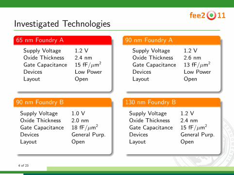
Investigated Technologies
65 nm Foundry A
Supply Voltage 1.2 VOxide Thickness 2.4 nmGate Capacitance 15 fF/µm2
Devices Low PowerLayout Open
90 nm Foundry A
Supply Voltage 1.2 VOxide Thickness 2.6 nmGate Capacitance 13 fF/µm2
Devices Low PowerLayout Open
90 nm Foundry B
Supply Voltage 1.0 VOxide Thickness 2.0 nmGate Capacitance 18 fF/µm2
Devices General Purp.Layout Open
130 nm Foundry B
Supply Voltage 1.2 VOxide Thickness 2.4 nmGate Capacitance 15 fF/µm2
Devices General Purp.Layout Open
4 of 23

Intrinsic Gain
• It represents the maximumgain obtainable from a singletransistor
Intrinsic Gain =gmgds∝ αL
• gm channel transconductance
• gds output conductance
• α scaling factor 0
10
20
30
40
50
60
0.05 0.1 0.15 0.2 0.25
130 nm Foundry B 90 nm Foundry B 65 nm Foundry A
Intri
nsic
Gai
nAs-drawn Gate Length [µm]
NMOSVDS=1.0 V
IC0=10
• Devices in the plot are biased at the same inversion level expressed by the InversionCoefficient IC0=ID/(I∗ZW /L) where I∗Z is the characteristic normalized drain current
• The intrinsic gain
◦ is proportional to the channel length
◦ is maintained across technology nodes (Lmin scales by the same factor α)
5 of 23

Intrinsic Gain in 65 nm node
10
100
1000
0.001 0.01 0.1 1 10 100
Intri
nsic
Gai
n
Inversion Coefficient
Weak Moderate Strong
L=65 nm
L=100 nm
L=130 nm
L=200 nm
L=350 nm
L=700 nm L=500 nm
0
50
100
150
200
250
300
350
400
0 0.1 0.2 0.3 0.4 0.5 0.6 0.7 0.8
Intri
nsic
Gai
n
As-drawn Gate Length [µm]
IC0=0.1
IC0=1
IC0=10
Weak
Moderate
Strong
DIBL effectsdominate on gds
CLM effectsdominate on gds
• As a function of the Inversion Coefficient, the intrinsic gain:
◦ is independent of the drain current in weak inversion
◦ decreases with the drain current in strong inversion
• As a function of the Channel Length, the intrinsic gain:
◦ is proportional to the channel length for L close to Lmin (DIBL dominates on gds)
◦ shows a reduced slope for L>5Lmin (CLM effects dominate on gds)6 of 23
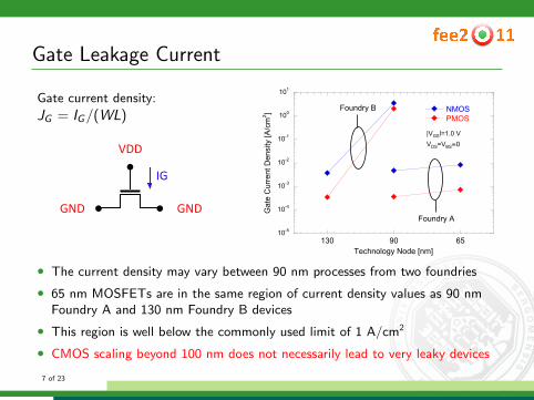
Gate Leakage Current
Gate current density:
JG = IG/(WL)
!"# !"#
$##
%!
10-5
10-4
10-3
10-2
10-1
100
101
130 90 65
NMOS APMOS ANMOS BPMOS B
Gat
e C
urre
nt D
ensi
ty [A
/cm
2 ]
Technology Node [nm]
Foundry A
Foundry B
|VGS|=1.0 VVDS=VBS=0
• The current density may vary between 90 nm processes from two foundries
• 65 nm MOSFETs are in the same region of current density values as 90 nmFoundry A and 130 nm Foundry B devices
• This region is well below the commonly used limit of 1 A/cm2
• CMOS scaling beyond 100 nm does not necessarily lead to very leaky devices
7 of 23

Noise in MOS Transistor
Noise in the drain current of a MOSFET can be represented through an equivalent
noise voltage source in series with the device gate
Oct. 29 – Nov. 4, 2006 – San Diego, California 2006 IEEE Nuclear Science Symposium
5
!"#$%&#'!"#$%&#' ()*+()*+ ,-.'$#$,"-$,-.'$#$,"-$
S
D
G
(f)SS(f)S 21/f
2W
2e +=
!" # $%&'()*+&,(
- .%/**(0)'%(12/0)*+&,()32/&*).+*'1&45'&+*)&*)'%().+*,&6(1(6)+7(1/'&*8).+*6&'&+*,9
- .+*'1&45'&+*,):1+2)7/1/,&'&.)1(,&,'/*.(,
!;<: # ;<:)*+&,(
- '(.%*+0+8=)6(7(*6(*').+*'1&45'&+*
"%&'( /*6);<:)*+&,( %/>()4((*)2(/,51(6)+*)'(,')6(>&.(,)with different geometries and biased at different drain currents
?+&,()&*)'%()61/&*).511(*')+:)/)@A!BCD)./*)4()1(71(,(*'(6)'%1+58%)/*)(E5&>/0(*')*+&,()>+0'/8(),+51.()&*),(1&(,)$&'%)'%()6(>&.()8/'(
m
B2ch
g
T4kS
!=
- FG G+0'H2/**I,).+*,'/*'
- D))/4,+05'()'(27(1/'51(
- ! .%/**(0)'%(12/0)*+&,())))).+(::&.&(*'
fWLfC
k(f)S
OX
f21/f "=
- F: ;<:)*+&,()7/1/2('(1
- !: ;<:)*+&,(),0+7(#1(0/'(6).+(::&.&(*'
White and 1/f noise have been measured on test devices with different geometries
and biased at different drain currents8 of 23

White noise
Evaluated in terms of the equivalent channel thermal noise resistance:
Req =S2W
4kBT= αw
nγ
gm
• αW excess noise coefficient
• n proportional to ID (VGS ) subthreshold characteristic
• γ channel thermal noise coefficient
• αW ≈1 for N and PMOS with L>65 nm ⇒ no sizable short channel effects
in the considered operating regions (for 65 nm devices αW≈1.3)
• Negligible contributions from parasitic resistances9 of 23

Noise in different CMOS nodes
• NMOSFETs belonging to different
CMOS nodes, with the minimum L
allowed by each process
• Since the oxide thickness tox and
the minimum L scale with the same
coefficient, the NMOSFETs feature
approximatively the same value of
the gate capacitance CG=WLCox
1
10
100
103 104 105 106 107 108
W/L=600/0.065 @ 65 nm Foundry A W/L=600/0.10 @ 90 nm Foundry BW/L=600/0.13 @ 130 nm Foundry B
Noi
se V
olta
ge S
pect
rum
[nV
/Hz1/
2 ]
Frequency [Hz]
NMOSCGATE ~ 1 pFID = 100 µA
• 1/f noise: devices exhibit a similar 1/f noise ⇒ the value of the Kf
parameter changes little across different CMOS generations
• White noise: devices are biased close to weak inversion ⇒ white noise isnot sizably affected by L and CMOS node variations even at minimumgate lengths, as it appears in the high frequency portion of the spectra
10 of 23

Ionizing radiation effects in sub-100 nm CMOSRadiation induced positive charge is removed from thin gate oxides by tunneling (which
also prevents the formation of interface states)
! In this work irradiation tests on 65 nm CMOS devices at different total ionizing doses provide insight into mechanisms governing the impact of gate and lateral isolation and of scaling-related technological advances on noise and its sensitivity to total ionizing dose effects.
! The behavior of the 1/f noise term is correlated with the effects on the drain current that irradiation brings along by turning on lateral parasitic transistors.
! A comparison with data from previous CMOS generations is carried out to assess the impact of process features on radiation-induced degradation effects.
! The MOSFETs studied in this work belong to a 65 nm LP (Low Power) CMOS process from a commercial vendor.
! The equivalent oxide thickness tOX is 1.95 nm and the maximum allowed supply voltage VDD is +1.2 V for standard core devices.
! We characterized PMOS and NMOS devices with gate lengths L from 65 nm to 700 nm and widths W from 20 !m to 1000 !m. The devices were designed with a standard open, interdigitated layout with gate finger of 5 !m for every geometry except for the devices with W=1000 !m, where a finger of 10 !m was used.
! A first set of devices was irradiated up to 10 Mrad(SiO2) total dose with !-rays from a 60Co source with a dose rate of about 8 rad(SiO2)/s. A second set of devices was exposed to a total dose of 5 Mrad(SiO2) of 10-keV X-rays from a 50 kV X-ray machine with a dose rate of 500 rad (SiO2)/s.
! The MOSFETs were biased during irradiation in the worst-case condition, that is, with all terminals grounded, except the gate of the NMOS, which was kept at VDD.
! For comparison purposes, this work also reports irradiation data for general purpose (GP) devices in the 130 nm (HCMOS9) and 90 nm (CMOS90) process from STM. !
!"#$%
&'"()%
*+,'-$%
).%
).%
/+01%
*23%
4"()%#'")5(5#+'%%6)7$'%
*+,'-$%
&'"()%
!"#$%
8"#$'"0%/"'"5(9-%%:$;(-$5%<=(#$%"''+>5?%
%*+,'-$@:'"()%%0$"A"7$%/"#=5%%
! In an interdigitated device, this can be modeled considering that two lateral transistors for each finger are turned on.
! The total gate width of the main transistor is W=n . Wfinger
• n is the total number of fingers
• Wfinger is the finger width.
! The two lateral parasitic transistors have: • an effective gate width Wlat,finger
• the same gate length L as the main device
• a gate oxide capacitance COX,lat inversely proportional to an effective oxide thickness tOX,lat
Introduction
Experimental Details
Parasitic Device Model
Mechanisms of Noise Degradation in Low Power 65 nm CMOS Transistors Exposed to Ionizing Radiation !Valerio Re1, Luigi Gaioni3, Massimo Manghisoni1, Lodovico Ratti2, Gianluca [email protected], [email protected], [email protected], [email protected], [email protected]
"#$%&!'(##)&*!+*$,-!'.$#$-*)#%/,-/!
Experimental Results
! This paper studied ionizing radiation effects on the noise performance of a 65 nm CMOS technology for the first time. Experimental data led to an understanding of different TID effects in gate and STI oxides, which result in a degradation of noise parameters.
! In the Low Power transistors we examined in this work, data analysis does not point out any novel damage mechanism which could be related to the technological advances associated to an aggressively scaled process. The comparison with data from previous CMOS generations confirms the high degree of tolerance to ionizing radiation that appears to be typical of sub-100 nm technologies.
! Variations of parameters for lateral leakage current and 1/f noise are associated to process details concerning the STI oxide and the doping of the STI sidewall. These features may be dependent on the specific foundry, so a certain degree of variation may be expected in different technologies inside the same CMOS node. !
Conclusion
2010 IEEE NUCLEAR AND SPACE RADIATION EFFECTS CONFERENCE, July 19-23, 2010 Denver, Colorado (USA)!
!"#$%& '"()*+%& $,%-).*! "#$%&#! '&&()'(*'%+! */0& ($*#&!#,-%./&#! )"& *& 0! 1&()! *%*(2! )%.#! %$! 34&(5.& 1".& */&!234& 5#)6& 789:;<<8<=>& #/& )6*& ?>& /@& ,."-%$$& *)&!67809!µ:!
012!34%/)!%&!356+789/!
012!!34%/)!%&!:56+789/!
;&$<=/%/!42!012!34%/)!:$#$>)*)#/!
10-11
10-10
10-9
10-8
10-7
10-6
10-5
10-4
10-3
-0.2 0 0.2 0.4 0.6
NMOS W/L = 200/0.50V
DS=0.6V
ID,lat @ 10 Mrad gamma raysID,lat @ 5 Mrad gamma raysID,lat @ 5 Mrad X-rays
Dra
in C
urre
nt [A
]
Gate-to-Source Voltage [V]
10-10
10-8
10-6
10-4
10-2
100
-0.2 0 0.2 0.4 0.6 0.8 1
NMOS W/L = 1000/0.13V
DS=0.6V
total ID after irradiationID before irradiationID,lattotal ID after irradiationID before irradiationID,lat
Dra
in C
urre
nt[A
]
Gate-to-Source Voltage [V]
130 nm
65 nm
1
10
100
103 104 105 106 107 108
NMOS W/L=200/0.50@ Id=50 µA, Vds=0.6 V
before irradiation5 Mrad
Noi
se V
olta
ge S
pect
rum
[nV
/Hz1/
2 ]
Frequency [Hz]
1
10
100
103 104 105 106 107 108
NMOS W/L=200/0.50@ Id=500 µA, Vds=0.6 V
before irradiation5 Mrad
Noi
se V
olta
ge S
pect
rum
[nV
/Hz1/
2 ]
Frequency [Hz]
1
10
100
103 104 105 106 107 108
NMOS W/L=200/0.35@ Id=20 µA, Vds=0.6 V
before irradiation10 Mrad
Noi
se V
olta
ge S
pect
rum
[nV
/Hz1/
2 ]
Frequency [Hz]
1
10
100
103 104 105 106 107 108
NMOS W/L=200/0.35@ Id=250 µA, Vds=0.6 V
before irradiation10 Mrad
Noi
se V
olta
ge S
pect
rum
[nV
/Hz1/
2 ]
Frequency [Hz]
1
10
100
103 104 105 106 107 108
NMOSPMOS
Noi
se V
olta
ge S
pect
rum
[nV
/Hz1/
2 ]
Frequency [Hz]
65 nm transistors W/L=200/0.10@ ID=100 µA, VDS=0.6 V
1
10
100
103 104 105 106 107 108
PMOS W/L=200/0.35@ Id=20 µA, |Vds|=0.6 V
before irradiation10 Mrad
Noi
se V
olta
ge S
pect
rum
[nV
/Hz1/
2 ]
Frequency [Hz]
! In NMOS edge effects due to radiation-induced positive charge in the STI oxide generate sidewall leakage paths.
7"#$%
*23%
#BCD0"#DE"F%
#BCD0"#DE()%
3);$'#$:%'$7(+)%"#%*23%5(:$>"00%
23&%():,-$:%/+5(9;$%-="'7$%
G@#1/$%5,H5#'"#$%
The total current flowing in the parasitic transistors of all device fingers can be obtained as:
• ID,lat current flowing in the parasitic transistors of all device fingers (negligible before irradiation).
• ID,tot drain current measured after irradiation. • ID,main current in the main transistor measured before irradiation
(unaffected by ionizing radiation)!7&('+!;/&&#+*!"1& )6%&%AB#'*(%/)&,*.*$#)#-& ).*/$#$)".&*$&(! $/+;*'%+!%$!*<#! =(*#4*%4.%/&;#! >%2*(=#! ?@A& -"@,*.%0& 5#)6& )6%& *%*(2! )&('+!;/&&#+*&"1&)6%&!234&@%*$B.%0&C%1".%&*/0&*1)%.&#..*0#*)#"/&
! ID,lat is smaller in transistors irradiated with X-rays. This may be ascribed to the smaller fractional yield of 10 keV X-rays with respect to 60Co γ-rays and/or to a possible enhanced low dose rate sensitivity effect in the edge devices.
! Small further effects can be noticed between 5 and 10 Mrad. Degradation effects appeared to approach their peak values after the exposure to a few Mrad total dose. This may be a hint of a saturation effect at high TID in the radiation-induced build-up of positive charge in the STI oxide.
ID,lat=ID,tot – ID,main= 2nID,lat,finger
7&('+!;/&&#+*!67B2(*&"1&)6%&%AB#'*(%/)&,*.*$#)#-&).*/$#$)".&*$&(!$/+;*'%+!%$!*<#!=(*#4*%4.%/&;#!>%2*(=#!?@A&*)&0#D%.%/)&)")*(&#"/#E#/+&0"$%$&1".&*&?>&/@&!234&@%*$B.%0&C%1".%&*/0&*1)%.&#..*0#*)#"/&5#)6&F&*/0&!G.*H$=&
7&('+! ;/&&#+*! *$& (! $/+;*'%+! %$! *<#! =(*#4*%4.%/&;#! >%2*(=#! ?@A&C%1".%&*/0&*1)%.&%I,"$B.%&)"&*&J<&2.*0&)")*(&0"$%&!G.*H$&1".&!234&5#)6& 789& :& J<<<8<=JK& #/& )6%& 9L& ?>& /@& ,."-%$$& */0& #/& *& JK<& /@&)%-6/"("+H=&&
! The LP 65 nm NMOS have a larger threshold voltage VTH, which also affects the behavior of the lateral parasitic transistors after irradiation. Actually, the threshold voltage is adjusted by a dedicated implant which reflects on the doping level at the STI sidewalls. As a result, also the lateral parasitic transistors turn on at a higher VGS. ! A meaningful comparison of the radiation tolerance of LP 65 nm NMOS and of transistors in less scaled nodes can be achieved by compensating for the different threshold voltage.
A')#C(22! ;/&&#+*! 67B2(*BD+=#&& #/& *& 0%'#-%& M/+%.& *$& (! $/+;*'%+! %$! *<#!%>#&)&'>#!>%2*(=#!?@AE?F<!*)& J<&2.*0& )")*(& #"/#E#/+&0"$%& &"1&!G.*H$&1".&!234NOP$&#/&JK<&/@Q&R<&/@&*/0&?>&/@&,."-%$$%=&&
! A larger amount of lateral leakage takes place in 130 nm devices. The smaller ID,lat,finger of 90 nm and 65 nm devices suggests that the sensitivity to positive charge buildup in STI oxides is mitigated by the higher doping of the P-type body with respect to less scaled processes.
! 65 nm devices appear to feature a larger lateral leakage current as compared to their 90 nm counterparts in the subthreshold region of the parasitic transistors. This could be a hint that some critical process parameters such as the doping along the STI sidewalls follow different scaling rules in LP transistors.
!"#$%& '"()*+%& $,%-).*! "#$%&#! '&&()'(*'%+! */0& ($*#&!#,-%./&#! *%! (! 0! 1&()! *%*(2! )%.#! %$! 34&(5.& 1".& */&!234& 5#)6& 789:;<<8<=>& #/& )6*& ?>& /@& ,."-%$$& *)!678099!µ:!
!"#$%& '"()*+%& $,%-).*! "#$%&#! '&&()'(*'%+! */0& ($*#&!#,-%./&#! *%! (! G9! 1&()! *%*(2! )%.#! %$! H4&(5.& 1".& */&!234& 5#)6& 789:;<<8<=K>& #/& )6*& ?>& /@& ,."-%$$& *)!678I9!µ:!
!"#$%& '"()*+%& $,%-).*! "#$%&#! '&&()'(*'%+! */0& ($*#&!#,-%./&#! *%! (! G9! 1&()! *%*(2! )%.#! %$! H4&(5.& 1".& */&!234& 5#)6& 789:;<<8<=K>& #/& )6*& ?>& /@& ,."-%$$& *)!678I09!µ:!
! The effect of ionizing radiation on the white term of the noise voltage spectrum is very small, if any. This is in agreement with the small radiation-induced variation of the drain current, which results in a little change of the transconductance gm.
! A 1/f noise increase is observed in irradiated devices at low drain current density, whereas at higher currents the degradation is almost negligible.
! This is a clear hint that the underlying mechanism is associated to the 1/f noise contribution from the lateral parasitic transistors turned on by radiation-induced charge buildup in STI oxides.
! The impact of these parasitic devices on the total drain current of the main transistor is larger at small current densities ID(L/W).
! At larger drain currents, the effects associated to lateral transistors become negligible, and the very little (if any) increase of 1/f noise confirms the high degree of ionizing radiation hardness that is intrinsic to a gate oxide about 2 nm thick.
J(*'%!%$! GK$! +%'.#! *#&L.!*1)%.& #..*0#*)#"/& S*)& '*.#"B$&PTUV& */0&C%1".%&#..*0#*)#"/&1".&!234NOP$&1."@&)6.%%&,."-%$$%$&5#)6&789&:&J<<<8<=JK&*)&67!8!9MG!L:!*/0!67!8!G!L:=&!
! Data in this plot clearly show the correlation between the effects on the lateral leakage current and on the 1/f noise as a function of TID, radiation source and CMOS process.
! As for the parameters associated to the current flowing along the STI, noise degradation data for the 65 nm LP devices are located between the values for the 130 nm and 90 nm NMOSFETs.
34%/)!54?)<!
Channel thermal noise (dominant at low current density) and noise in parasitic resistors
Kf = intrinsic process parameter, "f = 1/f noise slope. "f=1-1.2 for the PMOS and "f=0.85 for the NMOS. "f is independent of the device current ID and of the gate geometry
<=(#$%)+(5$% IJK%)+(5$%
The noise performances of a MOS device can be characterized in terms of the gate referred noise voltage spectrum:
!"#$%&'"()*+%&$,%-).*&C%1".%&#..*0#*)#"/&"1&!234&*/0&L234&5#)6&+*)%&5#0)6&7&:&;<<&W@&*/0&9&:&<=J<&W@&#/&)6%&9L&?>&/@&)%-6/"("+HQ&*)&TU&:&J<<&WX=&!
!"#$%&'"()*+%&$,%-).*&C%1".%&*/0&*1)%.&%I,"$B.%&)"&*&J<&2.*0&)")*(&0"$%&"1&?<Y"&Z[.*H$&1".&*&L234NOP&5#)6&789:;<<8<=K>&#/&)6%&?>&/@&,."-%$$&*)&TU:;<&WX=&!
! 65 nm LP devices show a very similar 1/f noise in PMOS and NMOS. This could be explained by the fact that the gate dielectric nitridation decreases the barrier energy experienced by holes across the silicon-dielectric interface.
! In PMOS positive charge buildup in STI oxides brings the N-type device bulk (N-well) deeper into accumulation, without creating any sidewall leakage. This means that after irradiation the 1/f noise term in the drain current is still entirely determined by the traps in the gate oxide. This results in a very small increase in the low-frequency part of the noise voltage spectrum, even at low current density, since radiation-induced positive charge is mostly removed from the gate oxide by tunneling before generating additional traps.
The 1/f component of the noise spectrum is given by the sum of the contribution S21/f,main from the main transistor and of the
contribution S21/f,lat from the equivalent transistor due to the effect of sidewall leakage in all device fingers:
• Kf,main and Kf,lat are intrinsic process parameters for the main device and the equivalent parasitic transistor.
• The sum of the transconductances of these two devices gives the total transconductance gm=gm,main+gm,lat
• The gate width of the equivalent parasitic transistor is Wlat=2 n Wlat,finger
• "f has the same value for main and lateral transistor before and after irradiation.
TID effects on the 1/f noise of the main device can be characterized by extracting the values of Kf,main before and after irradiation and by computing the ratio Kf,main,post/Kf,main,pre .
2$-=)+0+71% 23&%L4'":M% NKDE"()D/+5#%JNKDE"()D/'$% NKD0"#%LIO@PQM%
:56+! 356+! 356+!
0@A!&>!
0! &4*!!$B$%<$C<)! 0D@! EDA!
0A! 0D0! 0DF! EDA!
EA!&>!
0! &4*!!$B$%<$C<)! 0DG! FDH!
0A! 0D0! 0DH! 0@DA!
0AA!IJK#$=/L! 0D0! 0DG! MDA!
NH!&>!
H!IJK#$=/L! &4*!!$B$%<$C<)! 0DH! @DA!
H! 0D0! 0D@! @DA!
0A! 0D@! 0D@! FDA!From ID,lat curves as a function of VGS, it is possible to extract the values of geometrical and electrical parameters of the equivalent parasitic transistor modeling sidewall leakage, such as the values of the product Wlat,fingerCOX,lat at increasing TID, which gives additional information about radiation-induced edge effects. Both parameters Wlat,finger and tOX,lat depend on the extension of the inverted region along the STI.
O(%-).#-*(&,*.*@%)%.$&"1& (*)%.*(&,*.*$#)#-& ).*/$#$)".$&*)&0#D%.%/)&PTU&1".&!234NOP$& #/& )6%&9L&?>&/@&,."-%$$&*/0& #/&)6%&4P2&R<&/@&*/0&JK<&/@&Y234&,."-%$$%$=&&
! Wlat,fingerCOX,lat increases with TID. This can be explained considering that at low doses inversion takes place only at the bottom of the STI, where bulk doping is smaller; at increasing TID, the inverted region gradually extends towards the top of the STI. This increases both Wlat,finger and COX,lat, since the average oxide thickness controlling the lateral parasitic transistors decreases.
! Tthe larger effect of γ-rays on lateral leakage as compared to X-rays, and the different behavior of the three process that are considered here are confirmed.
! The small increase in Kf,main confirms the advantages related to the thin gate oxide in terms of radiation hardness. No significant difference can be detected among the different CMOS processes.
! Kf,lat changes more sizably, pointing out the different impact of irradiation in generating the traps in the STI oxide, which determine the magnitude of the 1/f noise associated to the lateral parasitic devices.
! Kf,lat is smaller in the 65 nm LP devices. This explains why at 10 Mrad their 1/f noise increase is similar to 90 nm transistors, in spite of the larger impact of lateral leakage currents on the overall drain current.
! PMOS do not exhibit any edge leakage, so Kf,lat is meaningless in this case. The 1/f noise increase associated to the gate oxide is very small. !
!N+'>#&.'*O!)'!P#&=(L%!!U#,=&0#&T/+%+/%.#*&T/0B$).#*(%!
6*(25!
I%
*23%
#BCD0"#DE"F%
3);$'#$:%'$7(+)%"#%*23%5(:$>"00%
#BCD0"#DE()%
23&%():,-$:%/+5(9;$%-="'7$% J81& /"#$%& ,*.*@%)%.$& 1".& !234& #..*0#*)%0& 5#)6& Q9R%& %$!!!!
H4&(5.&".&5#)6&J<[\%]&F[.*H$=!
N+'>#&.'*O!)'!S(>'(!U#,*.)#@%/)"&0#&O(%))."/#-*&
6*(25!!
P%
6TUT!4%E#"/%&0#&L*'#*&
!!!6*(25!!!!
R%
10-12
10-10
10-8
10-6
10-4
10-2
0 0.5 1
before irradiation5 MradID,latD
rain
Cur
rent
[A]
Gate-to-Source Voltage [V]
NMOS W/L = 200/0.50Vds = 0.6 V
1
10130 nm gamma rays65 nm gamma rays65 nm X-rays90 nm gamma rays130 nm gamma rays65 nm gamma rays65 nm X-rays90 nm gamma rays
1 10
S2 1/
f, po
st /
S2 1/
f, pr
e
Total Ionizing Dose [Mrad]
ID = 100 µA
ID = 1 mA
0.01
0.1
1 10
130 nm, gamma rays65 nm, gamma rays90 nm, gamma rays65 nm, X-rays
Wla
t,fin
ger C
OX
,lat [f
F/µ
m]
Total Ionizing Dose [Mrad]
10-11
10-10
10-9
10-8
10-7
10-6
10-5
-0.4 -0.3 -0.2 -0.1 0 0.1
NMOS fingerL = 0.13 µmV
DS=0.6V
130 nm
90 nm
65 nm
I D,la
t,fin
ger [A
]
VGS
- VTH
[V]
• Isolation oxides remain thick (orderof 100 nm) also in nanoscale CMOS,and they are radiation soft
• In NMOS edge effects due toradiation-induced positive charge inthe STI oxide generate sidewallleakage paths
• In an interdigitated device, this canbe modeled considering that twolateral transistors for each finger areturned on
• The effect of these parasitic device
on the noise and static
characteristics must be carefully
evaluated
11 of 23

Drain Current Static Characteristics
ID(VGS) before and after exposure to a 10 Mrad total dose of γ-rays
10-10
10-8
10-6
10-4
10-2
100
-0.2 0 0.2 0.4 0.6 0.8 1
NMOS W/L = 1000/0.13V
DS=0.6V
total ID after irradiationID before irradiationID,lattotal ID after irradiationID before irradiationID,lat
Dra
in C
urre
nt[A
]
Gate-to-Source Voltage [V]
130 nm
65 nm
• A larger amount of lateral leakage takes place in 130 nm devices
• The smaller ID,lat of 65 nm devices suggests that the sensitivity to positive chargebuildup in STI oxides is mitigated by the higher doping of the P-type body withrespect to less scaled processes
12 of 23

Noise in NMOSFETs
1
10
100
103 104 105 106 107 108
NMOS W/L=200/0.50@ Id=50 µA, Vds=0.6 V
before irradiation5 Mrad
Noi
se V
olta
ge S
pect
rum
[nV
/Hz1/
2 ]
Frequency [Hz]
1
10
100
103 104 105 106 107 108
NMOS W/L=200/0.50@ Id=500 µA, Vds=0.6 V
before irradiation5 Mrad
Noi
se V
olta
ge S
pect
rum
[nV
/Hz1/
2 ]
Frequency [Hz]
• Moderate 1/f noise increase at low current density, due to the contribution of lateralparasitic devices
• At higher currents the degradation is almost negligible because the impact of theparasitic lateral devices on the overall drain current is much smaller
• No increase in the white noise region is detected
• In PMOS, very small increase in the low-frequency part of the noise voltage spectrum,even at low current density
13 of 23

Remarks on 65 nm node
• Static, signal, noise measurements and radiation tests have beenperformed on devices belonging to a 65 nm CMOS process◦ Intrinsic gain is not degraded by scaling◦ Gate leakage current is well below the limit of 1 A/cm2
◦ Channel thermal noise behavior is consistent with equations valid inweak/moderate inversion
◦ Flicker noise comparison with previous CMOS nodes shows that scaling tothe 65 nm process does not affect 1/f noise performances significantly
◦ Radiation hardness tests confirm the high degree of tolerance to ionizingradiation that appears to be typical of sub-100 nm technologies
• At the 65 nm node, low-noise analog design, according to the study ofkey analog parameters, appears to be still viable
• We designed a prototype chip with mixed-signal readout circuits in a65 nm CMOS process manufactured by IBM ⇒ APSEL65
14 of 23
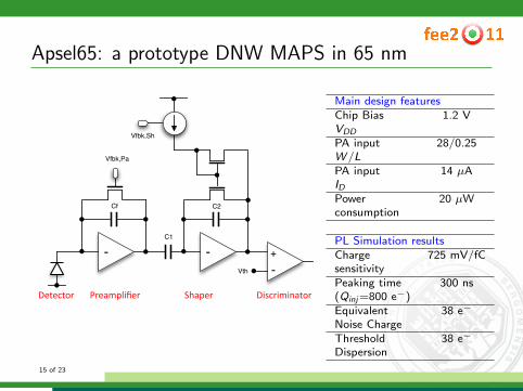
Apsel65: a prototype DNW MAPS in 65 nm
-Vth
-
Vfbk,Sh
!"#$%&'()#" *+$&#"
+
-
,(-."(%(/$01"
Vfbk,Pa
,#0#.01"
C2
C1
Cf
Main design featuresChip Bias 1.2 VVDD
PA input 28/0.25W /LPA input 14 µAIDPower 20 µWconsumption
PL Simulation resultsCharge 725 mV/fCsensitivityPeaking time 300 ns(Qinj=800 e−)Equivalent 38 e−
Noise ChargeThreshold 38 e−
Dispersion
15 of 23

Chip description
• CHi Standalone channels◦ Cinj=30 fF◦ Detector simulating cap
• CD=250 fF (CH1)
• CD=350 fF (CH2)
• CD=450 fF (CH3)
◦ DNW sensor not connected
• M1 3x3 matrix◦ 40 µm pixel pitch◦ all analog outputs accessible◦ Cinj=30 fF for the central pixel
◦ 360 µm2 DNW electrode area
• M2 8x8 matrix◦ 40 µm pixel pitch◦ row by row, 8 // digital readout
◦ 360 µm2 DNW electrode area
• FCi FFE channel◦ Cinj=10 fF◦ Detector simulating cap
• CD= 50 fF (FC1)
• CD=100 fF (FC2)
• CD=150 fF (FC3)• CD=100 fF (FC4)
enclosed layout PA input device
◦ DNW sensor not connected
16 of 23

Cell Layout
• Area 40×40 µm2
• DNW collecting electrode (orange)
◦ area 360 µm2
◦ capacitance 340 fF (estimated)◦ 99 % efficiency at VTh=400 e−
• In this prototype the digital sectionis kept to a minimum (latch, ORgate, tri-state buffer).
• It is planned to includesparsification and time-stampinglogic at the pixel level in moreadvanced versions (room for thisalready available)
17 of 23

Standalone Channels
-200
-150
-100
-50
0
0 1 2 3 4 5
600 e- 800 e-1000 e-1200 e-
Shap
er O
utpu
t [m
V]
Time [µs]
tp = 530 ns
Apsel65 - chip#1Standalone channel C
D=250 fF
Injected Charge
0
20
40
60
80
100
120
0 100 200 300 400 500 600 700 800
Cd=250 fFCd=350 fFCd=450 fF
Sha
per
Pea
k A
mpl
itude
[mV
]Input charge [electrons]
Apsel65 - chip#1MAPS standalone channels
GQ (Cd=250 fF) = 839 mV/fC
GQ (Cd=350 fF) = 809 mV/fC
GQ (Cd=450 fF) = 833 mV/fC
• Peaking time (at analog buffer output) is close to 530 ns for Qinj=800 e−
(simulation: tp=300 ns at shaper out, tp=420 ns at analog buffer out)
• Recovery time increases linearly with the signal amplitude (C2 is discharged by aconstant current)
• Charge sensitivity has an average value of about 830 mV/fC (725 mV/fC simulated)18 of 23

Noise in Standalone Channels
20
25
30
35
40
45
50
55
60
200 250 300 350 400 450 500
measurementsimulation
EN
C [e
- rm
s]
Detector capacitance [fF]
Apsel65 - chip#1MAPS standalone channels
• Measurement
ENC = 10.4+83e−/pF
• Simulation
ENC = 10.4+75e−/pF
• The ENC increases with the increase of the detector simulatingcapacitance
• Measured ENC is about 10% higher with respect to simulated values
19 of 23

3×3 Matrix
-120
-100
-80
-60
-40
-20
0
20
0 1 2 3 4 5
600 e-800 e-1000 e-Sh
aper
Out
put [
mV]
Time [µs]
Apsel65 - chip#13x3 matrix, pixel(2,2)
Injected Charge
tp = 460 ns
10
20
30
40
50
60
70
80
100 200 300 400 500 600 700 800
Sha
per
peak
am
plitu
de [m
V]
Input charge [electrons]
Apsel65 - chip#13x3 matrix - pixel (2,2)
GQ = 624 mV/fC
• Peaking time is close to 460 ns for Qinj=800 e−
• Recovery time does not increase linearly with the signal amplitude (non-optimalpolarization of the circuit)
• Charge sensitivity of 625 mV/fC was measured for the central pixel of the matrix
• Noise: ENC=67 e− for the central pixel and an average 54 e− for the other cells20 of 23

8×8 matrix
Threshold scan results
/ ndf 2 21.65 / 17Constant 3.09± 20.15 Mean 0.158± 5.859 Sigma 0.112± 1.267
noise [mV]0 2 4 6 8 10 12 14 16 18 20
Cou
nt
0
2
4
6
8
10
12
14
16
18
20
/ ndf 2 21.65 / 17Constant 3.09± 20.15 Mean 0.158± 5.859 Sigma 0.112± 1.267
noise histogram / ndf 2 8.492 / 17Constant 2.81! 18.34 Mean 0.7! 516.1 Sigma 0.523! 5.916
vth [mV]480 490 500 510 520 530 540 550 560
Cou
nt
0
2
4
6
8
10
12
14
16
18
20
/ ndf 2 8.492 / 17Constant 2.81! 18.34 Mean 0.7! 516.1 Sigma 0.523! 5.916
vth histogram
• Noise: ENC=59 e− rms (38 e− rms simulated)
• Threshold dispersion: σ(VTh) = 59 e− (38 e− rms simulated)
• Non-optimal polarization of the circuit
21 of 23

Fast Front-End Standalone ChannelsChannels conceived for the readout of high resistivity pixels
-60
-50
-40
-30
-20
-10
0
10
-0.1 0 0.1 0.2 0.3 0.4 0.5 0.6
8000 e-12000 e-16000 e-20000 e-
Shap
er O
utpu
t [m
V]
Time [µs]
Injected Charge
Apsel65 - chip#2FEE Channel C
D=50 fF
tp = 42 ns
-100
-80
-60
-40
-20
0
20
-0.1 0 0.1 0.2 0.3 0.4 0.5 0.6
8000 e-12000 e-16000 e-20000 e-24000 e-28000 e-32000 e-
Shap
er O
utpu
t [m
V]Time [µs]
Injected Charge
Apsel65 - chip#2FEE Channel PA Input DeviceEnclosed LayoutC
D=100 fF
tp = 50 ns
• Peaking time is close to 42 ns for Qinj=16000 e− (25 ns simulated)
• Charge sensitivity of about 18 mV/fC was measured (42 mV/fC simulated)
• Noise: ENC=165 e− rms (200 e− rms simulated)
22 of 23

Conclusions
• The 65 nm process is starting to be considered by designers for thedevelopment of readout ASICs at the next generation colliders
• Static, signal, noise measurements and radiation tests have beenperformed on devices belonging to a 65 nm CMOS process
• A test chip including DNW MAPS has been submitted in a 65 nm CMOSprocess provided by IBM
• Measurement results from this prototype circuit are encouraging andprovide useful information for future submissions and larger chips
• At the 65 nm nodes, low-noise analog design will pose challenges but,according to the study of key analog parameters and the prototype chipmeasurement results, appears to be still viable
23 of 23


