DESIGN AND REALIZATION OF A HIGH SPEED 64 X 64 – BIT...
86
DESIGN AND REALIZATION OF A HIGH SPEED 64 X 64 – BIT MULTIPLIER FOR LOW POWER APPLICATIONS by BERİL SEDA ÇİFTÇİ Submitted to the Graduate School of Engineering and Natural Sciences in partial fulfillment of the requirements for the degree of Master of Science Sabancı University Spring 2003
Transcript of DESIGN AND REALIZATION OF A HIGH SPEED 64 X 64 – BIT...
DESIGN AND REALIZATION OF A HIGH SPEED 64 X 64 – BIT
MULTIPLIER FOR LOW POWER APPLICATIONS
by
BERİL SEDA ÇİFTÇİ
Submitted to the Graduate School of Engineering and Natural Sciences
in partial fulfillment of
the requirements for the degree of
Master of Science
Sabancı University
Spring 2003

DESIGN AND REALIZATION OF A HIGH SPEED 64 X 64 – BIT
MULTIPLIER FOR LOW POWER APPLICATIONS
APPROVED BY:
Assoc. Prof. Dr. Yaşar GÜRBÜZ …………………….
(Thesis Supervisor)
Assist. Prof. Dr. Ayhan BOZKURT …………………….
Assist. Prof. Dr. Erkay SAVAŞ ……………………..
DATE OF APPROVAL: ………………………….

Beril Seda Çiftçi 2003
All Rights Reserved

To my parents

v
ACKNOWLEDGEMENTS
I would like to thank my supervisor, Assoc. Prof. Yaşar Gürbüz, for his
guidance, patience and encouragement throughout my research at Sabancı University.
His contributions and helpful comments enabled me to study more efficiently. I also
would like to thank my co-advisor, Assist. Prof. Ayhan Bozkurt, for his suggestions and
help.
I am grateful to Tuğba Demirci for sharing her all design experience with me,
answering my endless questions patiently and for her great friendship. Without her
efforts, I could have never succeeded in the end.
It was a great pleasure to work with all colleagues at Microelectronics Group. I
would like to thank Alper Emrah Üstünay, Aylin Ekşim, İhsan Çiçek, Mansoor Naseer
and Mustafa Parlak for their valuable contributions, friendship and support.
I would like to present my thanks to four special friends, Fatma Tepiroğlu,
Nihan Erol, Serdar Köroğlu and Verjin Karaoğlu, who have always been by my side
whenever I need them, from the very first day we have known each other. I’m thankful
for their unconditional love, trust and encouragement. I cannot imagine a life without
them.
I also wish to acknowledge all the faculty members, graduate students and other
individuals who have contributed to me during the period of my study at Sabancı
University. Especially, I would like to thank Arif Volkan Vural, Ayça Çeşmelioğlu,
Ekim Özaydın, Hacı Murat Özdemir, İpek Uzpeder, Özhan Öztürk, Sercan Uslu, Şenay
Mihçin, Yeşim Müge Şahin and Zafer Gürel for their intimate friendship. Also, thanks
to my late night workmates, Alper Gür, Ayşe Kıvılcım Coşkun, Didem Türker, Dilber
Ece Gamsız, Erdinç Öztürk and Özkan Öztürk, who gave me the courage and support
that I needed at the hardest aspects of my project.
Furthermore, I feel very lucky to have three precious friends in Sabancı
University; I would like to thank Hakan Göl, Mustafa Kerem Darıcı and Nuri Mehmet
Gökhan, for their invaluable friendship and for being my never-ending source of
motivation.
Finally, I will forever be grateful to my parents for their unconditional endless
love and for giving me the best of everything in the world. I would like to express my
appreciation, especially to my mother, for all their sacrifices and efforts. Without their
love and encouragement, all I could have achieved would be a complete failure.
vi
DESIGN AND REALIZATION OF A HIGH SPEED 64 X 64 – BIT MULTIPLIER
FOR LOW POWER APPLICATIONS
ABSTRACT
Wireless communication systems, including third generation cellular radio
systems and wireless LANs, have become tremendously popular in recent years. These
systems can be implemented using various platforms, like digital signal processors,
ASICs and FPGAs. Most digital signal processing systems incorporate a multiplication
unit to implement algorithms such as correlations, convolution, filtering and frequency
analysis. These algorithms are used in applications such as finite impulse filters (FIR),
infinite impulse filters (IIR), discrete cosine transforms (DCT) and fast Fourier
transforms (FFT). Moreover, there has been a rapid increase in the popularity of
portable and wireless electronic devices, like laptop computers, portable video players
and cellular phones, which rely on embedded digital signal processors. Since the desire
is to design digital systems for communication applications at best performance without
power sacrifices, the need for high performance and low power multipliers is inevitable.
Since multiplication is one of the most critical operations in many computational
systems, there have been many algorithm proposals in the literature to perform
multiplication, each offering different advantages and having tradeoffs in terms of
speed, circuit complexity, area and power consumption. This thesis focuses on an ASIC
implementation of a multiplexer-based multiplication method, an efficient algorithm
which is applicable to low power applications. Recently, it has been proved that the
multiplexer-based multiplier outperforms the modified Booth multiplier both in speed
and power dissipation by 13% to 26%, due to small internal capacitance. After
analyzing the performance characteristics of conventional multiplier types, it is
observed that the one designed using multiplexer-based multiplication algorithm is
more advantageous, especially when the size of the multiplied numbers is small. In
order to verify the superiorities of this algorithm, we performed an implementation, in
which the bit size of the multiplicand and the multiplier is comparably large. Thus,

vii
realization of a 64 x 64–bit multiplier block has been done in 0.35µ CMOS technology
using Cadence Design Framework tools. The final multiplier structure operates at
12.8ns with an approximate dynamic power consumption of 1mW. Also, using the same
algorithm, another block of 32-bit x 32-bit multiplier is designed and is sent for
fabrication.

viii
ÖZET
Üçüncü nesil hücresel radyo sistemleri, kablosuz yerel bölge ağları gibi telsiz
haberleşme sistemleri son yıllarda büyük önem kazanmıştır. Bu sistemler, sayısal işaret
işlemciler, uygulamaya özgün tümdevreler (ASIC) ve alan-programlanabilir mantıksal
kapı dizileri (FPGA) gibi ortamlar kullanılarak gerçekleştirilebilir. Temeli çarpma
işlemine dayanan korelasyon, konvolüsyon, filtreleme ve frekans analizi gibi
haberleşme algoritmalarının gerçeklenmesi amacıyla, sayısal işaret işlemcilerin çoğunda
bir çarpma bloğu bulunur. Bu algoritmalar sonlu ve sonsuz dürtü yanıtlı süzgeçler,
ayrık kosinüs dönüşümleri ve hızlı Fourier dönüşümleri gibi uygulamalarda yaygın
olarak kullanılmaktadır. Bununla birlikte, tümleşik sayısal işaret işlemcilerle çalışan
dizüstü bilgisayarlar, kablosuz video oynatıcıları ve cep telefonları gibi
taşınabilir elektronik tüketim mallarına olan rağbet hızla artmaktadır.
Telekomünikasyon uygulamalarında hedef, güç tüketiminden ödün vermeden en yüksek
performansta çalışan sayısal devre tasarımı gerçekleştirmek olduğundan, yüksek
hızlı ve az güç tüketen çarpma devrelerine olan ihtiyaç kaçınılmazdır.
Çarpma, sayısal sistemlerin çoğunda yer alan en kritik işlemlerden biri
olduğundan, tarihte çarpma işlemini gerçeklemeye yarayan ve farklı hız, alan, güç
tüketimi ve devre karmaşıklığı özelliklerine sahip olan pek çok algoritma önerilmiştir.
Bu tez, düşük güç tüketimli devreler için elverişli bir algoritma olan çoğullayıcı tabanlı
çarpma yönteminin tümdevre (ASIC) uygulamasını içermektedir. Küçük iç kapasite
özelliğinden dolayı, çoğullayıcı tabanlı çarpıcıların Booth çarpıcılarından hız ve güç
tüketimi bağlamında %13 ila %26 oranında daha üstün olduğu teorik olarak
kanıtlanmıştır. Klasik çarpma devrelerinin performans karakteristikleri incelendiğinde
de, çoğullayıcı tabanlı çarpma algoritmasıyla tasarlanmış devrelerin, özellikle küçük
sayılarla işlem yaptığında, daha avantajlı olduğu görülmüştür. Bu algoritmanın
üstünlüklerini doğrulamak ve diğer yapılarla kıyaslamak amacıyla, daha büyük sayılarla

ix
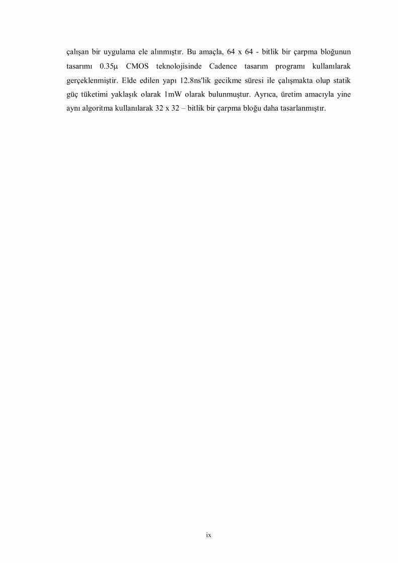
çalışan bir uygulama ele alınmıştır. Bu amaçla, 64 x 64 - bitlik bir çarpma bloğunun
tasarımı 0.35µ CMOS teknolojisinde Cadence tasarım programı kullanılarak
gerçeklenmiştir. Elde edilen yapı 12.8ns'lik gecikme süresi ile çalışmakta olup statik
güç tüketimi yaklaşık olarak 1mW olarak bulunmuştur. Ayrıca, üretim amacıyla yine
aynı algoritma kullanılarak 32 x 32 – bitlik bir çarpma bloğu daha tasarlanmıştır.

x
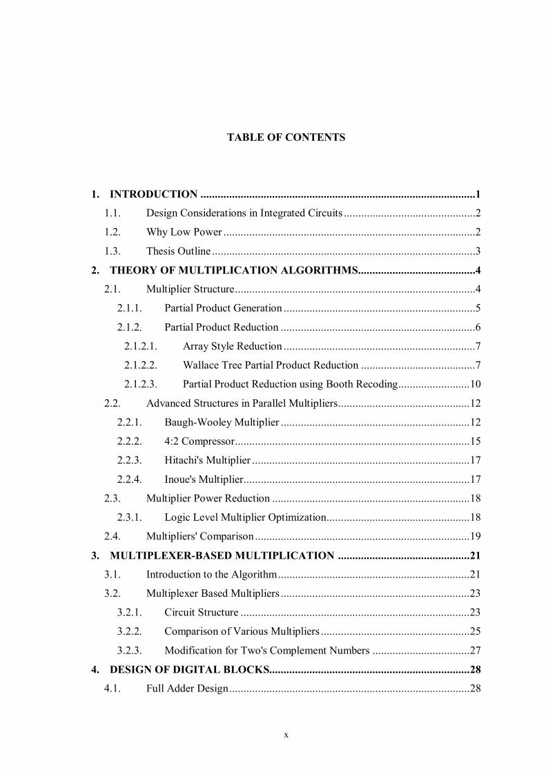
TABLE OF CONTENTS
1. INTRODUCTION ................................................................................................1
1.1. Design Considerations in Integrated Circuits ..............................................2
1.2. Why Low Power ........................................................................................2
1.3. Thesis Outline ............................................................................................3
2. THEORY OF MULTIPLICATION ALGORITHMS.........................................4
2.1. Multiplier Structure....................................................................................4
2.1.1. Partial Product Generation ...................................................................5
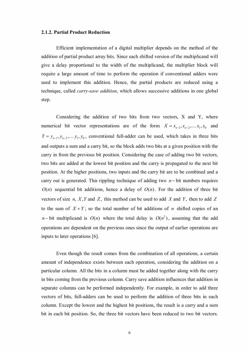
2.1.2. Partial Product Reduction ....................................................................6
2.1.2.1. Array Style Reduction ...................................................................7
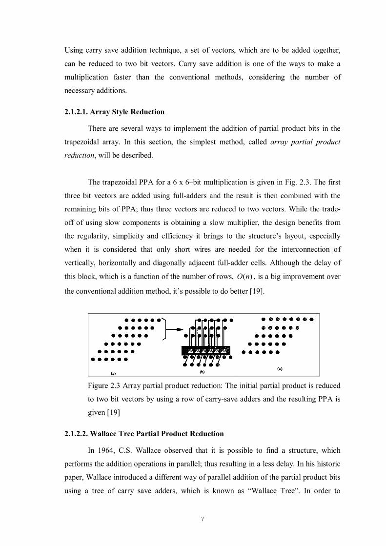
2.1.2.2. Wallace Tree Partial Product Reduction ........................................7
2.1.2.3. Partial Product Reduction using Booth Recoding.........................10
2.2. Advanced Structures in Parallel Multipliers..............................................12
2.2.1. Baugh-Wooley Multiplier ..................................................................12
2.2.2. 4:2 Compressor..................................................................................15
2.2.3. Hitachi's Multiplier ............................................................................17
2.2.4. Inoue's Multiplier...............................................................................17
2.3. Multiplier Power Reduction .....................................................................18
2.3.1. Logic Level Multiplier Optimization..................................................18
2.4. Multipliers' Comparison...........................................................................19
3. MULTIPLEXER-BASED MULTIPLICATION ..............................................21
3.1. Introduction to the Algorithm...................................................................21
3.2. Multiplexer Based Multipliers ..................................................................23
3.2.1. Circuit Structure ................................................................................23
3.2.2. Comparison of Various Multipliers ....................................................25
3.2.3. Modification for Two's Complement Numbers ..................................27
4. DESIGN OF DIGITAL BLOCKS......................................................................28
4.1. Full Adder Design....................................................................................28

xi
4.2. Multiplexer Design ..................................................................................33
4.3. Carry Lookahead Design..........................................................................37
4.4. Comparison of Multipliers' Simulation Results.........................................40
4.5. Design of 64 x 64-bit Multiplier Block.....................................................48
5. CONCLUSION ...................................................................................................52
6. REFERENCES ...................................................................................................53
xii
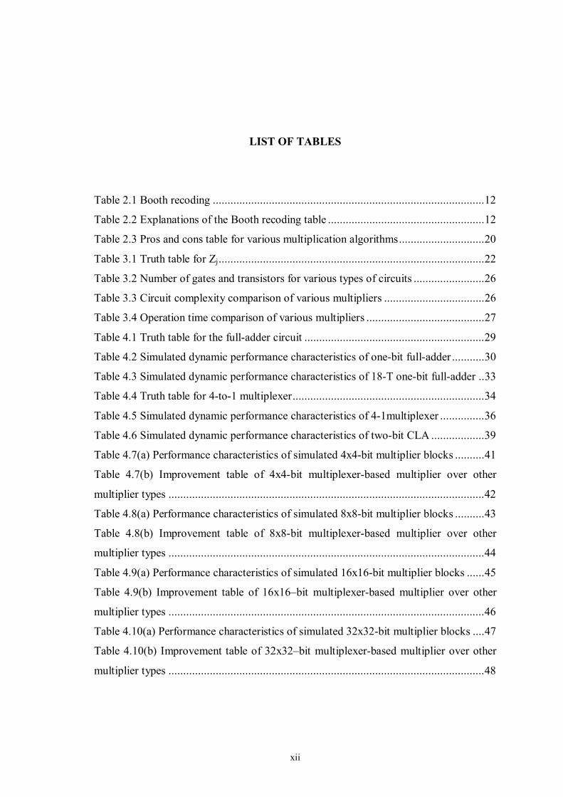
LIST OF TABLES
Table 2.1 Booth recoding ............................................................................................12
Table 2.2 Explanations of the Booth recoding table .....................................................12
Table 2.3 Pros and cons table for various multiplication algorithms.............................20
Table 3.1 Truth table for Zj..........................................................................................22
Table 3.2 Number of gates and transistors for various types of circuits ........................26
Table 3.3 Circuit complexity comparison of various multipliers ..................................26
Table 3.4 Operation time comparison of various multipliers ........................................27
Table 4.1 Truth table for the full-adder circuit .............................................................29
Table 4.2 Simulated dynamic performance characteristics of one-bit full-adder ...........30
Table 4.3 Simulated dynamic performance characteristics of 18-T one-bit full-adder ..33
Table 4.4 Truth table for 4-to-1 multiplexer.................................................................34
Table 4.5 Simulated dynamic performance characteristics of 4-1multiplexer ...............36
Table 4.6 Simulated dynamic performance characteristics of two-bit CLA ..................39
Table 4.7(a) Performance characteristics of simulated 4x4-bit multiplier blocks ..........41
Table 4.7(b) Improvement table of 4x4-bit multiplexer-based multiplier over other
multiplier types ...........................................................................................................42
Table 4.8(a) Performance characteristics of simulated 8x8-bit multiplier blocks ..........43
Table 4.8(b) Improvement table of 8x8-bit multiplexer-based multiplier over other
multiplier types ...........................................................................................................44
Table 4.9(a) Performance characteristics of simulated 16x16-bit multiplier blocks ......45
Table 4.9(b) Improvement table of 16x16–bit multiplexer-based multiplier over other
multiplier types ...........................................................................................................46
Table 4.10(a) Performance characteristics of simulated 32x32-bit multiplier blocks ....47
Table 4.10(b) Improvement table of 32x32–bit multiplexer-based multiplier over other
multiplier types ...........................................................................................................48
xiii
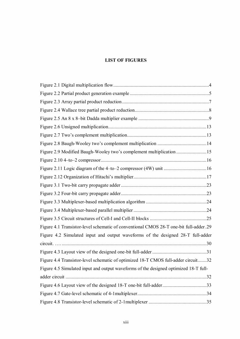
LIST OF FIGURES
Figure 2.1 Digital multiplication flow............................................................................4
Figure 2.2 Partial product generation example ...............................................................5
Figure 2.3 Array partial product reduction .....................................................................7
Figure 2.4 Wallace tree partial product reduction...........................................................8
Figure 2.5 An 8 x 8–bit Dadda multiplier example ........................................................9
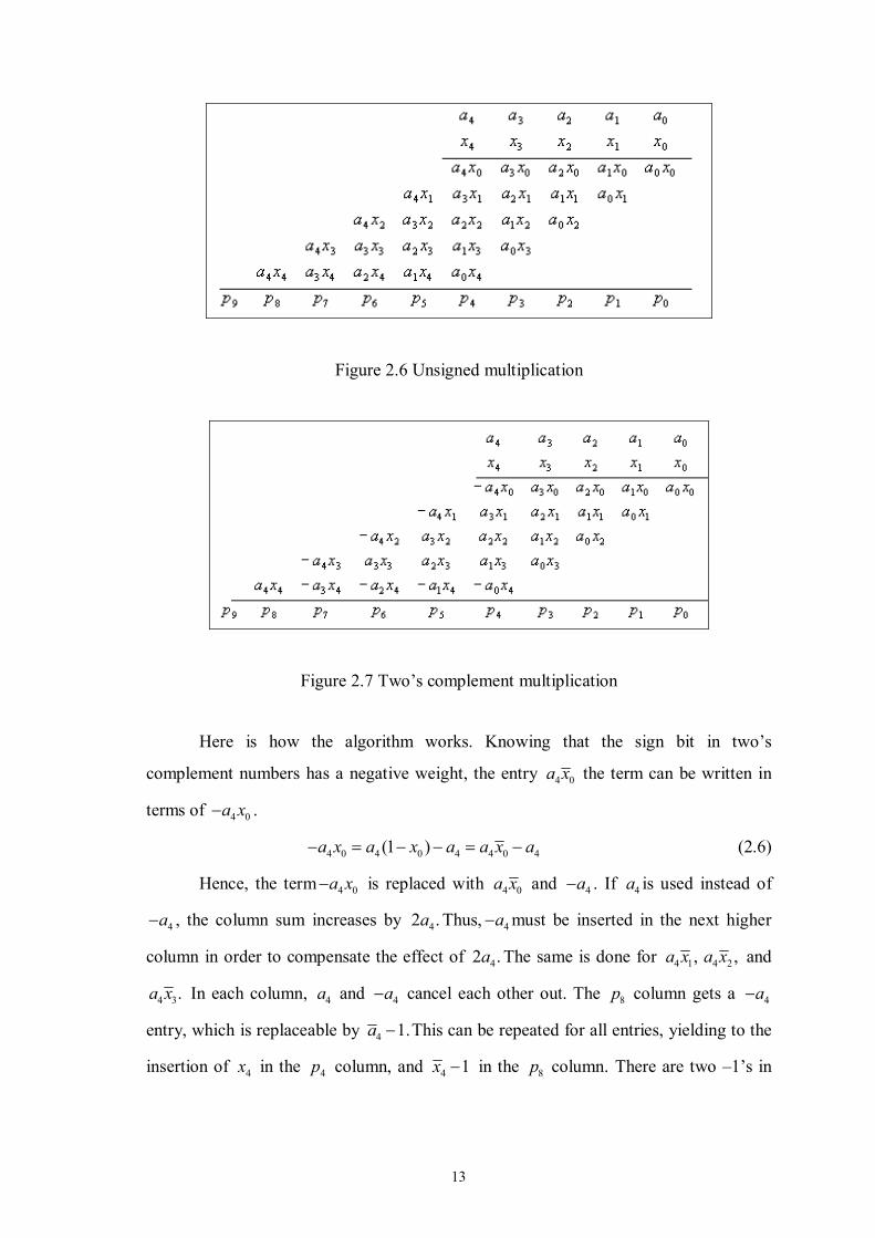
Figure 2.6 Unsigned multiplication..............................................................................13
Figure 2.7 Two’s complement multiplication...............................................................13
Figure 2.8 Baugh-Wooley two’s complement multiplication .......................................14
Figure 2.9 Modified Baugh-Wooley two’s complement multiplication ........................15
Figure 2.10 4–to–2 compressor....................................................................................16
Figure 2.11 Logic diagram of the 4–to–2 compressor (4W) unit ..................................16
Figure 2.12 Organization of Hitachi’s multiplier..........................................................17
Figure 3.1 Two-bit carry propagate adder ....................................................................23
Figure 3.2 Four-bit carry propagate adder....................................................................23
Figure 3.3 Multiplexer-based multiplication algorithm ................................................24
Figure 3.4 Multiplexer-based parallel multiplier ..........................................................24
Figure 3.5 Circuit structures of Cell-I and Cell-II blocks .............................................25
Figure 4.1 Transistor-level schematic of conventional CMOS 28-T one-bit full-adder .29
Figure 4.2 Simulated input and output waveforms of the designed 28-T full-adder
circuit. …. ...................................................................................................................30
Figure 4.3 Layout view of the designed one-bit full-adder ...........................................31
Figure 4.4 Transistor-level schematic of optimized 18-T CMOS full-adder circuit.......32
Figure 4.5 Simulated input and output waveforms of the designed optimized 18-T full-
adder circuit ................................................................................................................32
Figure 4.6 Layout view of the designed 18-T one-bit full-adder...................................33
Figure 4.7 Gate-level schematic of 4-1multiplexer.......................................................34
Figure 4.8 Transistor-level schematic of 2-1multiplexer ..............................................35

xiv
Figure 4.9 Schematic of 4-1multiplexer .......................................................................35
Figure 4.10 Simulated input and output waveforms of the multiplexer circuit ..............36
Figure 4.11 Layout view of the designed 4-1 multiplexer ............................................37
Figure 4.12 Schematic view of the designed two-bit CLA circuit.................................39
Figure 4.13 Simulated input and output waveforms of the two-bit CLA circuit ............39
Figure 4.14 Layout view of the designed CLA.............................................................40
Figure 4.15 Schematic view of the Cell-I Block...........................................................49
Figure 4.16 Layout view of the Cell-I Block................................................................49
Figure 4.17 Schematic view of the Cell-II Block .........................................................49
Figure 4.18 Layout view of the Cell-II Block ..............................................................50
Figure 4.19 Core layout of the 64 x 64–bit multiplier block .........................................50
Figure 4.20 Layout of 32 x 32–bit multiplier block......................................................51

DESIGN AND REALIZATION OF A HIGH SPEED 64 X 64 – BIT
MULTIPLIER FOR LOW POWER APPLICATIONS
by
BERİL SEDA ÇİFTÇİ
Submitted to the Graduate School of Engineering and Natural Sciences
in partial fulfillment of
the requirements for the degree of
Master of Science
Sabancı University
Spring 2003
DESIGN AND REALIZATION OF A HIGH SPEED 64 X 64 – BIT
MULTIPLIER FOR LOW POWER APPLICATIONS
APPROVED BY:
Assoc. Prof. Dr. Yaşar GÜRBÜZ …………………….
(Thesis Supervisor)
Assist. Prof. Dr. Ayhan BOZKURT …………………….
Assist. Prof. Dr. Erkay SAVAŞ ……………………..
DATE OF APPROVAL: ………………………….

Beril Seda Çiftçi 2003
All Rights Reserved

To my parents

v
ACKNOWLEDGEMENTS
I would like to thank my supervisor, Assoc. Prof. Yaşar Gürbüz, for his
guidance, patience and encouragement throughout my research at Sabancı University.
His contributions and helpful comments enabled me to study more efficiently. I also
would like to thank my co-advisor, Assist. Prof. Ayhan Bozkurt, for his suggestions and
help.
I am grateful to Tuğba Demirci for sharing her all design experience with me,
answering my endless questions patiently and for her great friendship. Without her
efforts, I could have never succeeded in the end.
It was a great pleasure to work with all colleagues at Microelectronics Group. I
would like to thank Alper Emrah Üstünay, Aylin Ekşim, İhsan Çiçek, Mansoor Naseer
and Mustafa Parlak for their valuable contributions, friendship and support.
I would like to present my thanks to four special friends, Fatma Tepiroğlu,
Nihan Erol, Serdar Köroğlu and Verjin Karaoğlu, who have always been by my side
whenever I need them, from the very first day we have known each other. I’m thankful
for their unconditional love, trust and encouragement. I cannot imagine a life without
them.
I also wish to acknowledge all the faculty members, graduate students and other
individuals who have contributed to me during the period of my study at Sabancı
University. Especially, I would like to thank Arif Volkan Vural, Ayça Çeşmelioğlu,
Ekim Özaydın, Hacı Murat Özdemir, İpek Uzpeder, Özhan Öztürk, Sercan Uslu, Şenay
Mihçin, Yeşim Müge Şahin and Zafer Gürel for their intimate friendship. Also, thanks
to my late night workmates, Alper Gür, Ayşe Kıvılcım Coşkun, Didem Türker, Dilber
Ece Gamsız, Erdinç Öztürk and Özkan Öztürk, who gave me the courage and support
that I needed at the hardest aspects of my project.
Furthermore, I feel very lucky to have three precious friends in Sabancı
University; I would like to thank Hakan Göl, Mustafa Kerem Darıcı and Nuri Mehmet
Gökhan, for their invaluable friendship and for being my never-ending source of
motivation.
Finally, I will forever be grateful to my parents for their unconditional endless
love and for giving me the best of everything in the world. I would like to express my
appreciation, especially to my mother, for all their sacrifices and efforts. Without their
love and encouragement, all I could have achieved would be a complete failure.

vi
DESIGN AND REALIZATION OF A HIGH SPEED 64 X 64 – BIT MULTIPLIER
FOR LOW POWER APPLICATIONS
ABSTRACT
Wireless communication systems, including third generation cellular radio
systems and wireless LANs, have become tremendously popular in recent years. These
systems can be implemented using various platforms, like digital signal processors,
ASICs and FPGAs. Most digital signal processing systems incorporate a multiplication
unit to implement algorithms such as correlations, convolution, filtering and frequency
analysis. These algorithms are used in applications such as finite impulse filters (FIR),
infinite impulse filters (IIR), discrete cosine transforms (DCT) and fast Fourier
transforms (FFT). Moreover, there has been a rapid increase in the popularity of
portable and wireless electronic devices, like laptop computers, portable video players
and cellular phones, which rely on embedded digital signal processors. Since the desire
is to design digital systems for communication applications at best performance without
power sacrifices, the need for high performance and low power multipliers is inevitable.
Since multiplication is one of the most critical operations in many computational
systems, there have been many algorithm proposals in the literature to perform
multiplication, each offering different advantages and having tradeoffs in terms of
speed, circuit complexity, area and power consumption. This thesis focuses on an ASIC
implementation of a multiplexer-based multiplication method, an efficient algorithm
which is applicable to low power applications. Recently, it has been proved that the
multiplexer-based multiplier outperforms the modified Booth multiplier both in speed
and power dissipation by 13% to 26%, due to small internal capacitance. After
analyzing the performance characteristics of conventional multiplier types, it is
observed that the one designed using multiplexer-based multiplication algorithm is
more advantageous, especially when the size of the multiplied numbers is small. In
order to verify the superiorities of this algorithm, we performed an implementation, in
which the bit size of the multiplicand and the multiplier is comparably large. Thus,

vii
realization of a 64 x 64–bit multiplier block has been done in 0.35µ CMOS technology
using Cadence Design Framework tools. The final multiplier structure operates at
12.8ns with an approximate dynamic power consumption of 1mW. Also, using the same
algorithm, another block of 32-bit x 32-bit multiplier is designed and is sent for
fabrication.

viii
ÖZET
Üçüncü nesil hücresel radyo sistemleri, kablosuz yerel bölge ağları gibi telsiz
haberleşme sistemleri son yıllarda büyük önem kazanmıştır. Bu sistemler, sayısal işaret
işlemciler, uygulamaya özgün tümdevreler (ASIC) ve alan-programlanabilir mantıksal
kapı dizileri (FPGA) gibi ortamlar kullanılarak gerçekleştirilebilir. Temeli çarpma
işlemine dayanan korelasyon, konvolüsyon, filtreleme ve frekans analizi gibi
haberleşme algoritmalarının gerçeklenmesi amacıyla, sayısal işaret işlemcilerin çoğunda
bir çarpma bloğu bulunur. Bu algoritmalar sonlu ve sonsuz dürtü yanıtlı süzgeçler,
ayrık kosinüs dönüşümleri ve hızlı Fourier dönüşümleri gibi uygulamalarda yaygın
olarak kullanılmaktadır. Bununla birlikte, tümleşik sayısal işaret işlemcilerle çalışan
dizüstü bilgisayarlar, kablosuz video oynatıcıları ve cep telefonları gibi
taşınabilir elektronik tüketim mallarına olan rağbet hızla artmaktadır.
Telekomünikasyon uygulamalarında hedef, güç tüketiminden ödün vermeden en yüksek
performansta çalışan sayısal devre tasarımı gerçekleştirmek olduğundan, yüksek
hızlı ve az güç tüketen çarpma devrelerine olan ihtiyaç kaçınılmazdır.
Çarpma, sayısal sistemlerin çoğunda yer alan en kritik işlemlerden biri
olduğundan, tarihte çarpma işlemini gerçeklemeye yarayan ve farklı hız, alan, güç
tüketimi ve devre karmaşıklığı özelliklerine sahip olan pek çok algoritma önerilmiştir.
Bu tez, düşük güç tüketimli devreler için elverişli bir algoritma olan çoğullayıcı tabanlı
çarpma yönteminin tümdevre (ASIC) uygulamasını içermektedir. Küçük iç kapasite
özelliğinden dolayı, çoğullayıcı tabanlı çarpıcıların Booth çarpıcılarından hız ve güç
tüketimi bağlamında %13 ila %26 oranında daha üstün olduğu teorik olarak
kanıtlanmıştır. Klasik çarpma devrelerinin performans karakteristikleri incelendiğinde
de, çoğullayıcı tabanlı çarpma algoritmasıyla tasarlanmış devrelerin, özellikle küçük
sayılarla işlem yaptığında, daha avantajlı olduğu görülmüştür. Bu algoritmanın
üstünlüklerini doğrulamak ve diğer yapılarla kıyaslamak amacıyla, daha büyük sayılarla
ix
çalışan bir uygulama ele alınmıştır. Bu amaçla, 64 x 64 - bitlik bir çarpma bloğunun
tasarımı 0.35µ CMOS teknolojisinde Cadence tasarım programı kullanılarak
gerçeklenmiştir. Elde edilen yapı 12.8ns'lik gecikme süresi ile çalışmakta olup statik
güç tüketimi yaklaşık olarak 1mW olarak bulunmuştur. Ayrıca, üretim amacıyla yine
aynı algoritma kullanılarak 32 x 32 – bitlik bir çarpma bloğu daha tasarlanmıştır.
x
TABLE OF CONTENTS
1. INTRODUCTION ................................................................................................1
1.1. Design Considerations in Integrated Circuits ..............................................2
1.2. Why Low Power ........................................................................................2
1.3. Thesis Outline ............................................................................................3
2. THEORY OF MULTIPLICATION ALGORITHMS.........................................4
2.1. Multiplier Structure....................................................................................4
2.1.1. Partial Product Generation ...................................................................5
2.1.2. Partial Product Reduction ....................................................................6
2.1.2.1. Array Style Reduction ...................................................................7
2.1.2.2. Wallace Tree Partial Product Reduction ........................................7
2.1.2.3. Partial Product Reduction using Booth Recoding.........................10
2.2. Advanced Structures in Parallel Multipliers..............................................12
2.2.1. Baugh-Wooley Multiplier ..................................................................12
2.2.2. 4:2 Compressor..................................................................................15
2.2.3. Hitachi's Multiplier ............................................................................17
2.2.4. Inoue's Multiplier...............................................................................17
2.3. Multiplier Power Reduction .....................................................................18
2.3.1. Logic Level Multiplier Optimization..................................................18
2.4. Multipliers' Comparison...........................................................................19
3. MULTIPLEXER-BASED MULTIPLICATION ..............................................21
3.1. Introduction to the Algorithm...................................................................21
3.2. Multiplexer Based Multipliers ..................................................................23
3.2.1. Circuit Structure ................................................................................23
3.2.2. Comparison of Various Multipliers ....................................................25
3.2.3. Modification for Two's Complement Numbers ..................................27
4. DESIGN OF DIGITAL BLOCKS......................................................................28
4.1. Full Adder Design....................................................................................28

xi
4.2. Multiplexer Design ..................................................................................33
4.3. Carry Lookahead Design..........................................................................37
4.4. Comparison of Multipliers' Simulation Results.........................................40
4.5. Design of 64 x 64-bit Multiplier Block.....................................................48
5. CONCLUSION ...................................................................................................52
6. REFERENCES ...................................................................................................53

xii
LIST OF TABLES
Table 2.1 Booth recoding ............................................................................................12
Table 2.2 Explanations of the Booth recoding table .....................................................12
Table 2.3 Pros and cons table for various multiplication algorithms.............................20
Table 3.1 Truth table for Zj..........................................................................................22
Table 3.2 Number of gates and transistors for various types of circuits ........................26
Table 3.3 Circuit complexity comparison of various multipliers ..................................26
Table 3.4 Operation time comparison of various multipliers ........................................27
Table 4.1 Truth table for the full-adder circuit .............................................................29
Table 4.2 Simulated dynamic performance characteristics of one-bit full-adder ...........30
Table 4.3 Simulated dynamic performance characteristics of 18-T one-bit full-adder ..33
Table 4.4 Truth table for 4-to-1 multiplexer.................................................................34
Table 4.5 Simulated dynamic performance characteristics of 4-1multiplexer ...............36
Table 4.6 Simulated dynamic performance characteristics of two-bit CLA ..................39
Table 4.7(a) Performance characteristics of simulated 4x4-bit multiplier blocks ..........41
Table 4.7(b) Improvement table of 4x4-bit multiplexer-based multiplier over other
multiplier types ...........................................................................................................42
Table 4.8(a) Performance characteristics of simulated 8x8-bit multiplier blocks ..........43
Table 4.8(b) Improvement table of 8x8-bit multiplexer-based multiplier over other
multiplier types ...........................................................................................................44
Table 4.9(a) Performance characteristics of simulated 16x16-bit multiplier blocks ......45
Table 4.9(b) Improvement table of 16x16–bit multiplexer-based multiplier over other
multiplier types ...........................................................................................................46
Table 4.10(a) Performance characteristics of simulated 32x32-bit multiplier blocks ....47
Table 4.10(b) Improvement table of 32x32–bit multiplexer-based multiplier over other
multiplier types ...........................................................................................................48

xiii
LIST OF FIGURES
Figure 2.1 Digital multiplication flow............................................................................4
Figure 2.2 Partial product generation example ...............................................................5
Figure 2.3 Array partial product reduction .....................................................................7
Figure 2.4 Wallace tree partial product reduction...........................................................8
Figure 2.5 An 8 x 8–bit Dadda multiplier example ........................................................9
Figure 2.6 Unsigned multiplication..............................................................................13
Figure 2.7 Two’s complement multiplication...............................................................13
Figure 2.8 Baugh-Wooley two’s complement multiplication .......................................14
Figure 2.9 Modified Baugh-Wooley two’s complement multiplication ........................15
Figure 2.10 4–to–2 compressor....................................................................................16
Figure 2.11 Logic diagram of the 4–to–2 compressor (4W) unit ..................................16
Figure 2.12 Organization of Hitachi’s multiplier..........................................................17
Figure 3.1 Two-bit carry propagate adder ....................................................................23
Figure 3.2 Four-bit carry propagate adder....................................................................23
Figure 3.3 Multiplexer-based multiplication algorithm ................................................24
Figure 3.4 Multiplexer-based parallel multiplier ..........................................................24
Figure 3.5 Circuit structures of Cell-I and Cell-II blocks .............................................25
Figure 4.1 Transistor-level schematic of conventional CMOS 28-T one-bit full-adder .29
Figure 4.2 Simulated input and output waveforms of the designed 28-T full-adder
circuit. …. ...................................................................................................................30
Figure 4.3 Layout view of the designed one-bit full-adder ...........................................31
Figure 4.4 Transistor-level schematic of optimized 18-T CMOS full-adder circuit.......32
Figure 4.5 Simulated input and output waveforms of the designed optimized 18-T full-
adder circuit ................................................................................................................32
Figure 4.6 Layout view of the designed 18-T one-bit full-adder...................................33
Figure 4.7 Gate-level schematic of 4-1multiplexer.......................................................34
Figure 4.8 Transistor-level schematic of 2-1multiplexer ..............................................35
xiv
Figure 4.9 Schematic of 4-1multiplexer .......................................................................35
Figure 4.10 Simulated input and output waveforms of the multiplexer circuit ..............36
Figure 4.11 Layout view of the designed 4-1 multiplexer ............................................37
Figure 4.12 Schematic view of the designed two-bit CLA circuit.................................39
Figure 4.13 Simulated input and output waveforms of the two-bit CLA circuit ............39
Figure 4.14 Layout view of the designed CLA.............................................................40
Figure 4.15 Schematic view of the Cell-I Block...........................................................49
Figure 4.16 Layout view of the Cell-I Block................................................................49
Figure 4.17 Schematic view of the Cell-II Block .........................................................49
Figure 4.18 Layout view of the Cell-II Block ..............................................................50
Figure 4.19 Core layout of the 64 x 64–bit multiplier block .........................................50
Figure 4.20 Layout of 32 x 32–bit multiplier block......................................................51

1
1. INTRODUCTION
Arithmetic circuits, like adders and multipliers, are essential components in the
design of communication circuits in ASIC. Recently, an overwhelming interest has been
seen in the problems of designing digital systems for communication systems and
digital signal processing with low power at no performance penalty. To design low-
power high-speed arithmetic circuits requires a combination techniques at four levels;
algorithm, architecture, circuit and system levels. This thesis presents an ASIC
implementation of a multiplication algorithm, which is suitable for high-performance
and low–power applications.
In microprocessors, multiplication operation is performed in a variety of forms
in hardware and software depending on the cost and transistor budget allocated for this
particular operation. In the beginning stages of computer development, any complex
operation was usually programmed in software or coded in the micro-code of the
machine and some limited assistance was provided. Today, it’s more likely to find full
hardware implementation of the multiplication in order to satisfy the growing demand
for speed and due to increasing cost of hardware.
Most digital signal processing (DSP) systems incorporate a multiplication unit to
implement algorithms such as correlations, convolution, filtering and frequency
analysis. In many DSP algorithms, the multiplier lies in the critical delay path and
ultimately determines the performance of the algorithm. The speed of multiplication
operation is of great importance in DSP as well as in the general processors today,
especially since the media processing took off. In the past, multiplication was
implemented generally with a sequence of addition, subtraction and shift operations.
Recently, many multiplication algorithms have been invented and developed, each
having pros and cons in different fields.

2
The multiplier is a fairly large block of a computing system. The amount of
circuitry involved is proportional to the square of its resolution; i.e. a multiplier of size n
bits has 2( )O n gates [2]. For multiplication algorithms performed in DSP applications,
latency and throughput are the two major constraints from delay perspective. Latency is
the real delay of computing a function, a measure of how long after the inputs to a
device are stable, is the final result available on outputs. Throughput is the measure of
how many multiplications can be performed in a given period of time. Multiplier is not
only a high-delay block but also a significant source of power dissipation. That’s why,
if one also aims to minimize power consumption, it is of great interest to identify the
techniques to be applied to reduce delay by using various delay optimizations.
1.1. Design Considerations in Integrated Circuits
After guaranteeing correct digital functionality, the primary consideration for
system designers has always been speed. A circuit is specified to operate at a particular
delay, otherwise the entire system may not work; further reduction is beneficial but not
strictly necessary. Other factors may have equal or greater importance than power
dissipation; area of implementation and reliability issues are subjects which designer
must take into account. It’s worth to note that power reduction techniques are not
necessarily negatively correlated to delay reduction. For example, one method to reduce
delay in a circuit’s critical path is to upsize the driving strength of gates, which results
in increased power reduction. However, reducing interconnect capacitance, which is
another way to lower delay, reduces both power and delay. Generally, great power
savings can be achieved if delay is not an issue, but optimizing power without delay
consideration is insignificant.
1.2. Why Low Power?
Power dissipation limitations come in two ways. The first is related to cooling
considerations when implementing high performance systems. High-speed circuits
dissipate large amounts of energy in a short amount of time, generating a great deal of
3
heat. This heat needs to be removed by the package on which integrated circuits are
mounted. Heat removal may become a limiting factor if the package cannot sufficiently
dissipate this heat or if the required thermal components are too expensive for the
application.
The second failure of high-power circuits relates to the increasing popularity of
portable electronic devices. Laptop computers, portable video players and cellular
phones all use batteries as a power source. These devices provide a limited time of
operation before they require recharging. To extend the battery life, low power
operation is desirable in integrated circuits.
1.3. Thesis Outline
This thesis focuses on an algorithm, called multiplexer based multiplication,
which is suitable for high-speed and low-power applications. The algorithm, which is
proposed by K. Pekmestzi, is symmetric so it’s very applicable for binary
multiplication, due to the interchangeability of the multiplicand and the multiplier. In
theory, it is proven that the algorithm is comparably faster than recently proposed ones
and much simpler than the others by means of circuit complexity. The implementation
of this algorithm is performed by designing a 64-bit x 64-bit multiplier block in 0.35µ
CMOS technology using Cadence Design Framework tools. Also, using the same
algorithm, another block of 32-bit x 32-bit multiplier is designed and is sent for
fabrication. The following chapters discuss the reason of using multiplexer–based
multiplication algorithm as well as the design details of the blocks. In chapter 2,
sequential multiplication basics, like forming the partial products and reducing the
number of partial product bits through the use of high-radix methods, and various
multiplication algorithms are introduced. The theory of multiplexer based multiplication
algorithm and the architectural structure of designed multiplier is explained in Chapter
3. Chapter 4 presents design stages of the multiplier block, including the simulation
results and layouts. Finally, in Chapter 5, conclusions are discussed.
4
2. THEORY OF MULTIPLICATION ALGORITHMS
In this chapter, we present a brief description of digital multipliers including
their structure and relevant components. Some techniques, which have been developed
to reduce the multiplier delay, are also discussed. Next, we go over power dissipation in
CMOS circuits, along with some basic techniques, which can be applied to reduce
power.
2.1. Multiplier structure
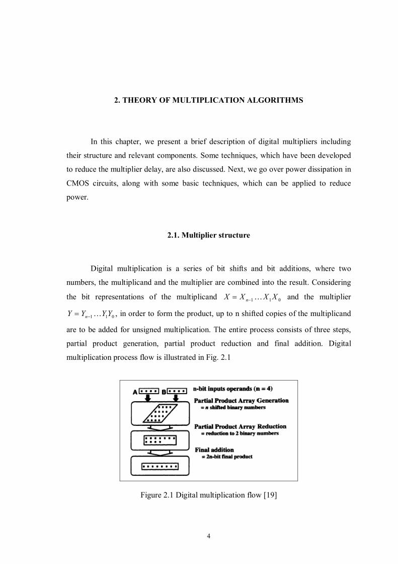
Digital multiplication is a series of bit shifts and bit additions, where two
numbers, the multiplicand and the multiplier are combined into the result. Considering
the bit representations of the multiplicand 011 XXXX n K−= and the multiplier
011 YYYY n K−= , in order to form the product, up to n shifted copies of the multiplicand
are to be added for unsigned multiplication. The entire process consists of three steps,
partial product generation, partial product reduction and final addition. Digital
multiplication process flow is illustrated in Fig. 2.1
Figure 2.1 Digital multiplication flow [19]
5
2.1.1 Partial Product Generation
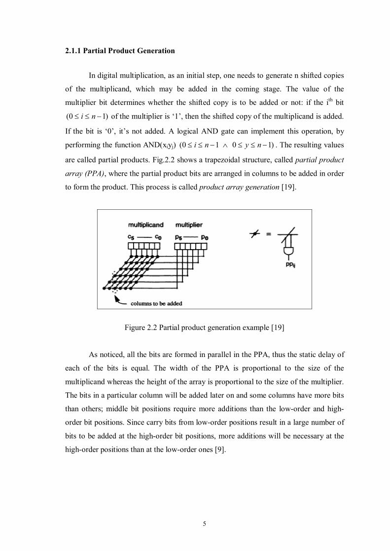
In digital multiplication, as an initial step, one needs to generate n shifted copies
of the multiplicand, which may be added in the coming stage. The value of the
multiplier bit determines whether the shifted copy is to be added or not: if the ith bit
)10( −≤≤ ni of the multiplier is ‘1’, then the shifted copy of the multiplicand is added.
If the bit is ‘0’, it’s not added. A logical AND gate can implement this operation, by
performing the function AND(xiyj) )1010( −≤≤∧−≤≤ nyni . The resulting values
are called partial products. Fig.2.2 shows a trapezoidal structure, called partial product
array (PPA), where the partial product bits are arranged in columns to be added in order
to form the product. This process is called product array generation [19].
Figure 2.2 Partial product generation example [19]
As noticed, all the bits are formed in parallel in the PPA, thus the static delay of
each of the bits is equal. The width of the PPA is proportional to the size of the
multiplicand whereas the height of the array is proportional to the size of the multiplier.
The bits in a particular column will be added later on and some columns have more bits
than others; middle bit positions require more additions than the low-order and high-
order bit positions. Since carry bits from low-order positions result in a large number of
bits to be added at the high-order bit positions, more additions will be necessary at the
high-order positions than at the low-order ones [9].
6
2.1.2. Partial Product Reduction
Efficient implementation of a digital multiplier depends on the method of the
addition of partial product array bits. Since each shifted version of the multiplicand will
give a delay proportional to the width of the multiplicand, the multiplier block will
require a large amount of time to perform the operation if conventional adders were
used to implement this addition. Hence, the partial products are reduced using a
technique, called carry-save addition, which allows successive additions in one global
step.
Considering the addition of two bits from two vectors, X and Y, where
numerical bit vector representations are of the form 1 2 1 0, , ,n nX x x x x− −= K and
1 2 1 0, , ,n nY y y y y− −= K , conventional full-adder can be used, which takes in three bits
and outputs a sum and a carry bit, so the block adds two bits at a given position with the
carry in from the previous bit position. Considering the case of adding two bit vectors,
two bits are added at the lowest bit position and the carry is propagated to the next bit
position. At the higher positions, two inputs and the carry bit are to be combined and a
carry out is generated. This rippling technique of adding two n− bit numbers requires
( )O n sequential bit additions, hence a delay of ( )O n . For the addition of three bit
vectors of size ,n ,X Y and ,Z this method can be used to add X and ,Y then to add Z
to the sum of X Y+ ; so the total number of bit additions of n shifted copies of an
n− bit multiplicand is ( )O n where the total delay is 2( )O n , assuming that the add
operations are dependent on the previous ones since the output of earlier operations are
inputs to later operations [6].
Even though the result comes from the combination of all operations, a certain
amount of independence exists between each operation, considering the addition on a
particular column. All the bits in a column must be added together along with the carry
in bits coming from the previous column. Carry save addition influences that addition in
separate columns can be performed independently. For example, in order to add three
vectors of bits, full-adders can be used to perform the addition of three bits in each
column. Except the lowest and the highest bit positions, the result is a carry and a sum
bit in each bit position. So, the three bit vectors have been reduced to two bit vectors.
7
Using carry save addition technique, a set of vectors, which are to be added together,
can be reduced to two bit vectors. Carry save addition is one of the ways to make a
multiplication faster than the conventional methods, considering the number of
necessary additions.
2.1.2.1. Array Style Reduction
There are several ways to implement the addition of partial product bits in the
trapezoidal array. In this section, the simplest method, called array partial product
reduction, will be described.
The trapezoidal PPA for a 6 x 6–bit multiplication is given in Fig. 2.3. The first
three bit vectors are added using full-adders and the result is then combined with the
remaining bits of PPA; thus three vectors are reduced to two vectors. While the trade-
off of using slow components is obtaining a slow multiplier, the design benefits from
the regularity, simplicity and efficiency it brings to the structure’s layout, especially
when it is considered that only short wires are needed for the interconnection of
vertically, horizontally and diagonally adjacent full-adder cells. Although the delay of
this block, which is a function of the number of rows, ( )O n , is a big improvement over
the conventional addition method, it’s possible to do better [19].
Figure 2.3 Array partial product reduction: The initial partial product is reduced
to two bit vectors by using a row of carry-save adders and the resulting PPA is
given [19]
2.1.2.2. Wallace Tree Partial Product Reduction
In 1964, C.S. Wallace observed that it is possible to find a structure, which
performs the addition operations in parallel; thus resulting in a less delay. In his historic
paper, Wallace introduced a different way of parallel addition of the partial product bits
using a tree of carry save adders, which is known as “Wallace Tree”. In order to
8
perform the multiplication of two numbers with the Wallace method, partial product
matrix is reduced to a two-row matrix by using a carry save adder and the remaining
two rows are summed using a fast carry-propagate adder to form the product.
Parallelizing carry save operations yields a delay proportional to the logarithm of the
operand size n ( )(log 2/3 nO ), which is significantly shorter than the array’s sequential
operations [6]. However, the disadvantage of Wallace trees is their irregular layout with
respect to array structures. Moreover, this irregular layout results in greater wire loads.
Also it’s worth to note that the width of the final adder in a Wallace tree structure is
approximately nn 2/3log2 − whereas the width of array architectures uses an adder
having a width of n. In Fig 2.4, an example of 6-bit x 6-bit multiplication using Wallace
tree partial product reduction method is shown. It can be noticed that parallelizing two
carry save operations results in a smaller PPA after just one step [10].
Figure 2.4 Wallace tree partial product reduction [19]
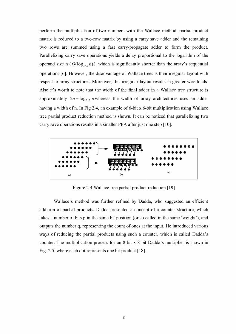
Wallace’s method was further refined by Dadda, who suggested an efficient
addition of partial products. Dadda presented a concept of a counter structure, which
takes a number of bits p in the same bit position (or so called in the same ‘weight’), and
outputs the number q, representing the count of ones at the input. He introduced various
ways of reducing the partial products using such a counter, which is called Dadda’s
counter. The multiplication process for an 8-bit x 8-bit Dadda’s multiplier is shown in
Fig. 2.5, where each dot represents one bit product [18].

9
Figure 2.5 An 8 x 8–bit Dadda multiplier example [10]
In Dadda’s multiplier, columns having more than six digits (or having tend to
grow more than six digits due to carry bits) are reduced by using half and full-adders. A
half adder takes two input digits and outputs one bit in the same column and one in the
next more significant column, whereas a full-adder takes three inputs bits and outputs
two digits; again one in the same, one in the next column. The arrangement of half and
full-adders are done in such a way that no column in the first matrix will have more than
six dots. In the second reduction matrix, the maximum number of digits in one column
is four. In the coming stages, third matrix contains at most three digits and the fourth
matrix has two digits per column. In order to find out the maximum number of digits in
one column of the matrix, we start from the final two-row matrix and limit the height of
each matrix no more than 1.5 times the height of its successor [10]. The delay of the
matrix reduction process is proportional to )log(n , since the number of matrices is
logarithmically related to the number of bits in the words to be multiplied. In other
words, the total delay of the multiplier is proportional to the logarithm of the word size,
due to the addition process in the final two-row matrix, which can be implemented
using a carry lookahead adder, which also has a logarithmic delay. There has been a
great research for making faster parallel multipliers however, the efforts for inventing
the fastest counter structure could not go beyond an architecture, which performs the
summation of partial products faster than a full-adder [7].

10
2.1.2.3. Partial Product Reduction Using Booth Recoding
One of the best-known variations of the multiplication algorithm is the “Booth’s
Recoding Algorithm” described by Booth in 1951. The algorithm allows reducing the
number of partial products, hence speeding up the multiplication process. The Booth’s
algorithm can be used for both sign magnitude and unsigned numbers. Before the
explanation of Booth’s algorithm, brief information about radix multiplication will be
presented.
Radix multiplication
For a given range of numbers to be represented, a higher representation radix
leads to fewer digits. Thus, a digit at a time multiplication requires fewer cycles as we
move to higher radices. That’s why, high radix multiplication algorithms are studied for
implementing hardware. A k-bit binary number can be formulated as a 2/k -digit
radix-4 number and a 3/k -digit radix-8 number and so on. The use of high radix
multiplication involves dealing with more than one bit of the multiplier in one cycle.
Higher radix multipliers are designed to reduce the number of adders and hence the
delay required to compute the partial sums. The best-known method is called Booth
recoding, which a radix-4 multiplication scheme [9].
Booth recoding technique
Under certain conditions, when a bit in the multiplier is ‘0’, a bench of carry
save adders does not perform a useful function, because a ‘0’ is added to the carry save
result. Thus, the input bits are propagated to the output bits. These carry save adders can
be removed from the multiplier structure in this case, resulting in power and delay
settings. However, since it’s not possible to know exactly which bits of the multiplier
will be ‘0’, the case, when all the multiplier bits are ‘1’, has to be considered to
maintain generality. Furthermore, in the largest delay case, for example in 4 x 4–bit
multiplication, circuitry must be provided for the case when the multiplier is ‘1111’,
which results in a delay of four stages. Considering that multiplying by ‘1111’ is the
same as multiplying by ‘10000’ and subtracting the multiplicand form the result, and
knowing that multiplying by a power of two is simply a shift, the worst case delay has
been reduced to 2-stages from 4-stages. This type of stage reduction is known as Booth
recoding [2]. The theory of the Booth algorithm is explained below.

11
Modified Booth algorithm
Consider two n-bit numbers X and Y to be multiplied. Y can be expressed as: 1 2 0
1 2 02 2 2n nn nY Y Y Y− −− −= − + + +L (2.1)
21 2 3
43 4 5
01 0 1
( 2 ) 2
( 2 ) 2
( 2 )2
nn n n
nn n n
Y Y Y Y
Y Y Y
Y Y Y
−− − −
−− − −
−
= − + +
+ − + + + +
+ − + +
L (2.2)
where 01 =−Y and 33
42
23 2222 −
−−
−−
− =− nn
nn
nn YYY have been used in the expression. Eq.
(2.2) can be represented by
∑∑−=
=
−=
=−+ ⋅=⋅++−=
12
0
21
2
0
212212 22)2(
ni
i
ii
ni
i
iiii yYYYY (2.3)
Thus,
⋅+−
⋅+−=⋅ ∑∑
−
=
−−
−
=
−−
2
0
11
2
0
11 2222
n
j
jj
nn
n
i
ii
nn YYXXYX (2.4)
⋅
⋅+−=⋅ ∑∑
−
=
−
=
−−
12
0
22
0
11 222
n
j
jj
n
i
ii
nn yXXYX (2.5)
From the sequence of ii YY 212 ,+ and 12 −iY , ,iy which can be –2, –1, 0, 1, 2 can be
known. Therefore, the partial products of n-bit x n-bit multiplication can be reduced to
the effective multiplication of n-bit x 2n -bit multiplication. Thus, the multiplication time
is also reduced. The relation between ,12 +iY ,2iY 12 −iY and iy can be summarized in
Table 2.1 and the explanations of the five possible multiples of the multiplicand are
given in Table 2.2 [11].
Booth recoding necessitates the internal use of two’s complement representation
in order to efficiently perform subtraction of the partial products as well as additions.
Since it is easy to implement, the algorithm is widely used for two’s complement
multiplication. The advantage of Booth algorithm is that it generates roughly one half of
the partial products when compared to other multiplier implementations, however this
benefit comes at the expense of increased hardware complexity.
12
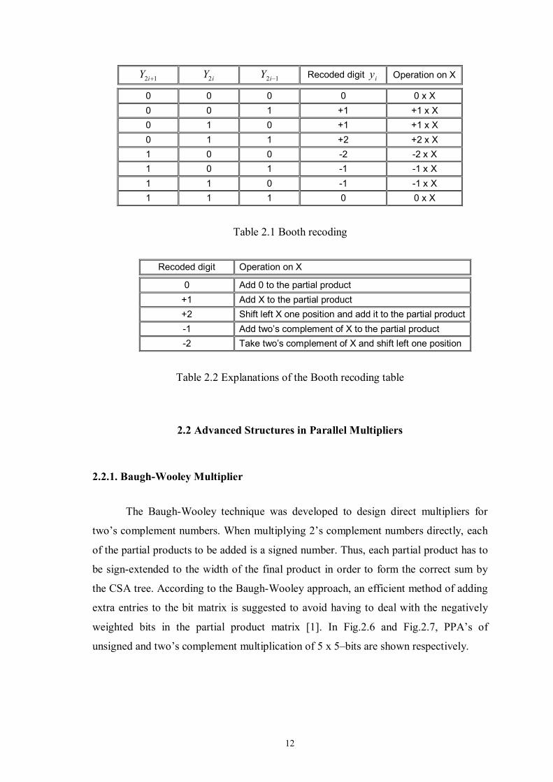
2 1iY + 2iY 12 −iY Recoded digit iy Operation on X
0 0 0 0 0 x X 0 0 1 +1 +1 x X 0 1 0 +1 +1 x X 0 1 1 +2 +2 x X 1 0 0 -2 -2 x X 1 0 1 -1 -1 x X 1 1 0 -1 -1 x X 1 1 1 0 0 x X
Table 2.1 Booth recoding
Recoded digit Operation on X
0 Add 0 to the partial product +1 Add X to the partial product +2 Shift left X one position and add it to the partial product-1 Add two’s complement of X to the partial product -2 Take two’s complement of X and shift left one position
Table 2.2 Explanations of the Booth recoding table
2.2 Advanced Structures in Parallel Multipliers
2.2.1. Baugh-Wooley Multiplier
The Baugh-Wooley technique was developed to design direct multipliers for
two’s complement numbers. When multiplying 2’s complement numbers directly, each
of the partial products to be added is a signed number. Thus, each partial product has to
be sign-extended to the width of the final product in order to form the correct sum by
the CSA tree. According to the Baugh-Wooley approach, an efficient method of adding
extra entries to the bit matrix is suggested to avoid having to deal with the negatively
weighted bits in the partial product matrix [1]. In Fig.2.6 and Fig.2.7, PPA’s of
unsigned and two’s complement multiplication of 5 x 5–bits are shown respectively.
13
Figure 2.6 Unsigned multiplication
Figure 2.7 Two’s complement multiplication
Here is how the algorithm works. Knowing that the sign bit in two’s
complement numbers has a negative weight, the entry 4 0a x the term can be written in
terms of 4 0a x− .
4 0 4 0 4 4 0 4(1 )a x a x a a x a− = − − = − (2.6)
Hence, the term 4 0a x− is replaced with 4 0a x and 4a− . If 4a is used instead of
4a− , the column sum increases by 42 .a Thus, 4a− must be inserted in the next higher
column in order to compensate the effect of 42 .a The same is done for 4 1,a x 4 2 ,a x and
4 3.a x In each column, 4a and 4a− cancel each other out. The 8p column gets a 4a−
entry, which is replaceable by 4 1.a − This can be repeated for all entries, yielding to the
insertion of 4x in the 4p column, and 4 1x − in the 8p column. There are two –1’s in
14
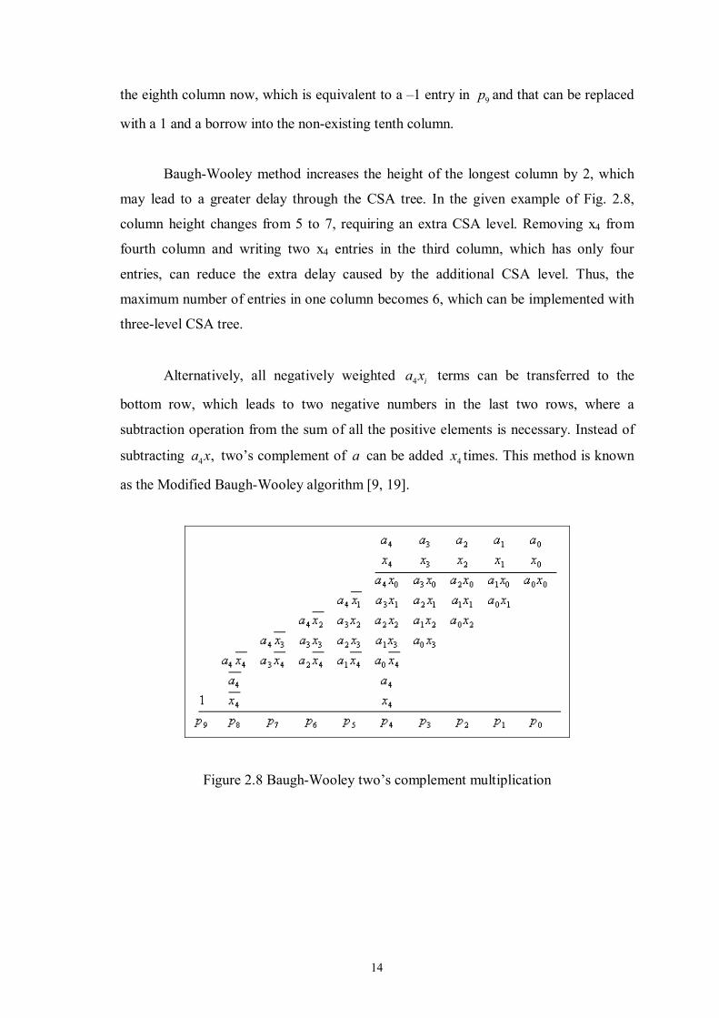
the eighth column now, which is equivalent to a –1 entry in 9p and that can be replaced
with a 1 and a borrow into the non-existing tenth column.
Baugh-Wooley method increases the height of the longest column by 2, which
may lead to a greater delay through the CSA tree. In the given example of Fig. 2.8,
column height changes from 5 to 7, requiring an extra CSA level. Removing x4 from
fourth column and writing two x4 entries in the third column, which has only four
entries, can reduce the extra delay caused by the additional CSA level. Thus, the
maximum number of entries in one column becomes 6, which can be implemented with
three-level CSA tree.
Alternatively, all negatively weighted 4 ia x terms can be transferred to the
bottom row, which leads to two negative numbers in the last two rows, where a
subtraction operation from the sum of all the positive elements is necessary. Instead of
subtracting 4 ,a x two’s complement of a can be added 4x times. This method is known
as the Modified Baugh-Wooley algorithm [9, 19].
Figure 2.8 Baugh-Wooley two’s complement multiplication

15
Figure 2.9 Modified Baugh-Wooley two’s complement multiplication
Modified form of the Baugh-Wooley method, shown in Fig. 2.9, is more
preferable since it does not increase the height of the columns in the matrix. However,
this type of multiplier is suitable for applications where operands with less than 16 bits
are processed, like digital filters where small operands like 6, 8 or 12 bits are used.
Baugh-Wooley scheme becomes slow and area consuming when operands are greater
than or equal to 16-bits. So, different techniques are required in order to reduce the size
of the array as well as maintaining the regularity.
2.2.2. 4:2 Compressor
In the ‘4-2 carry save module’ structure, which is introduced by Weinberger in
1981, a complicated-interconnected combination of full-adder cells exist for performing
the compression of partial products faster than counters. In fact, the structure
compresses five partial product bits (four input bits and one carry–in bit) into three,
however it acts as a compressor reducing the four bits into two, since carry-in and carry-
out bits connect the adjacent 4:2 compressors [13]. Thus, the number of partial product
bits is reduced by half in one stage, making the efficiency higher. The structure of 4:2
compressors is shown in Fig. 2.10.

16
Figure 2.10 4–to–2 compressor
Figure 2.11 Logic diagram of the 4–to–2 compressor (4W) unit
In the arrangement shown in Fig. 2.10, sum can be obtained via four XOR gate
delays
( )[ ][ ] inCXXXXS ⊕⊕⊕⊕= 4321 (2.7)
which is identical to the result in the Wallace tree structure using 2-layer carry save
adders, thus the equation can be rearranged as
( )[ ] inin CCXXXS ⊕⊕⊕⊕= )( 421 (2.8)
In the circuit shown with Fig.2.11, the equations are obtained to be
1 2 3 4outC I I I I= ⋅ + ⋅ (2.9)
( ) ( )1 2 1 2 3 4 3 4 inS I I I I I I I I C= + ⊕ + ⊕ (2.10)
[ ]1 2 3 4 3 2 3 4 1 2 3 4( ) ( ) ( ) ( ) inC I I I I I I I I I I I I C= ⋅ ⋅ ⋅ + ⊕ ⋅ ⊕ + ⊕ ⊕ ⊕ (2.11)

17
2.2.3. Hitachi’s Multiplier
One of the best-performance multipliers, proposed by Ohkubo and Suzuki [13],
is a 0.25µm 54 x 54-bit multiplier with an operation time of 4.4ns. The architecture
consists of blocks performing Wallace tree and Booth’s algorithms as well as a carry-
lookahead adder, which is shown in Fig. 2.12. Booth’s algorithm is used in order to save
from chip area instead of reducing delay time, and by using Wallace tree operation time
reduction is performed. Moreover, for further improvement, a new 4:2 compressor type
is developed with pass transistor multiplexers so that critical path gate stages are
reduced. This yields to reduction in the multiplication time of the multiplier by 14%
[11].
Figure 2.12 Organization of Hitachi’s multiplier [13]
2.2.4. Inoue’s Multiplier
Among recently designed multipliers, the one published by Inoue [16] is one of
the fastest. The novelty of this multiplier is the new design of the Booth encoder and
Booth selector blocks for the generation of partial products, and the 4:2 compression
unit. A simpler implementation of these blocks removes the need to use an XOR gate in
the critical path. The regular Booth selector requires 18 transistors per bit for the
implementation where the modified Booth selector necessitates 10 transistors per bit.
Although for the 54-bit x 54-bit multiplier modification of the Booth selector yields
44% reduction in the transistor count, this modification does not give a significant
18
change by means of transistor count in the overall multiplier, since the number of
transistors that the Booth encoder consists of is approximately 1.2% of total
architecture.
In his paper [16], Inoue observed the possible 26 implementations of the 4:2
compressor and among them he chose the one, which has the minimum number of
transistors. Reducing the transistor count by 24% not only saves from layout area but
also reduces the speed of the multiplier, approximately by 5% of the fastest possible
implementation.
2.3. Multiplier Power Reduction
The design of digital CMOS has focused on delay reduction and power
dissipation. In multipliers, delay increases as the size of the multiplier grows in terms of
bits, but it can vary depending on the implementation. Power is proportional to the
amount of circuitry of the multiplier and the way that it is connected to perform the
multiplication. Since the amount of adder blocks is proportional to the square of the size
of the number of bits 2( )n , multipliers tend to be fairly large, power consuming blocks.
Dynamic power consumption of digital CMOS circuits is expressed by Eq.
(2.12). Static power consumption is neglected because which is relatively too small. The
static power comes from the pull-up resistor. This would mean that in complementary
CMOS circuits, only one device is conducting at a time. So, there’s no need to calculate
static power; only dynamic power exists since there is never a direct path between VDD
and GND in steady state.
2
dyn DD op n n DD scn n
P = V f C + V iα∑ ∑ (2.12)
n being the number of nodes and alpha is the number of switching activities. An
equivalent equation can be expressed as
2dyn L DD op sc DD peak op DD leakageP = C V f + t V I f + V I (2.13)
19
In this equation, Ipeak determined by the saturation current of the pmos and nmos
transistors, which depend on their sizes, process technology, temperature, etc. and the
ratio between input and output slopes. When load capacitance is small, power is
dominated by Isc, short circuit current. Isc is less than 10% of total dynamic current
under the condition of fast rising time and falling time. Therefore short circuit current is
neglected for convenience of calculation. Because supply voltage and operation
frequency are fixed when the application is specified, the power consumption is
determined by node capacitance and transition activities (probability). In considering
these two parameters, equivalent capacitance is defined in Eq (2.14). Using the principle
of uniform distribution of delay time, the equivalent capacitance can be expressed as the
driving load (CL). If it is only driving a capacitive load, then we can approximate that all
the power is consumed in the act of switching. It is nontrivial to calculate the power via
the resistance of the on transistor so use the output capacitance.
2
dyn L DD opP = C V f (2.14)
Typically, power and delay minimization techniques focus on the various sub-
blocks inside a larger block and address power optimization of these blocks
independently. However, an integrated approach may be more helpful since dependency
of these blocks affect the overall power characteristics.
2.3.1. Logic Level Multiplier Optimization
Booth recoding suffers from the problem that unequal delay paths exist in the
Booth partial product generator. One path goes from the multiplier through the Booth
encoder and then to the Booth decoder, while paths from the multiplicand go directly to
the Booth decoder. Since the Booth decoder is composed of two gates a glitch can result
at the output of the Booth decoder due to this greater delay. One approach is to redesign
the Booth encoder/decoders such that Booth encoder’s logic depth is reduced and early
arriving signal coming from the multiplicand has a greater delay through the decoder
that inputs from the encoder. This balances the signal paths and allows reducing of
glitches [2].

20
2.4. Multipliers’ Comparison
In this chapter, we presented recently developed various multiplication
algorithms. Generally, it is not possible to say that an exact architecture yields to greater
cost-effectiveness, since the trade-off is design and technology dependent. The basic
array multipliers, like the Baugh-Wooley scheme, consume low power and exhibit
relatively good performances, however their use is limited with 16 bits. For operands of
16-bits and over, the modified Booth algorithm reduces the partial product’s numbers
by half. Thus, the speed of the multiplier is reduced. Due to the circuitry overhead in the
Booth algorithm, its power dissipation is comparable to the Baugh-Wooley multiplier.
Wallace’s strategy for building carry save adder (CSA) trees is to combine the partial
product bits as early as possible, whereas in Dadda’s method, combination of partial
products is performed at the latest stage. This method yields to a simpler CSA tree and a
wider carry-propagate adder while the designs using Wallace’s method are the fastest
ones. However, a logarithmic depth reduction tree based on CSA’s has an irregular
structure that makes the design and layout more difficult. Moreover, connections and
signal paths of varying lengths may lead to logical hazards and signal skew that have
implications for both performance and power consumption. That’s why; alternative
reduction trees that are more suitable for VLSI implementation are of interest. A
summary of pros and cons of the proposed algorithms, based on their theoretical
attributes, is given below in Table 2.3 in terms of speed, circuit complexity, layout
regularity and silicon area. A detailed simulation-based analysis of the algorithms, for
both small-size and large-size multiplier blocks, will be presented in section 4.4. In the
next chapter, we will introduce another multiplication algorithm called multiplexer
based multiplication, which has both high-speed and low-power opportunity.
Multiplier Type Speed Circuit Complexity Layout Area Array Low / Medium Simple Regular Smallest Booth High Complex Irregular Medium
Wallace Higher Medium More irregular Large Dadda Higher Medium Irregular Medium Hitachi Highest More complex Medium regularity Largest Inoue Highest More complex Irregular Largest
Table 2.3 Pros and cons table for various multiplication algorithms
21
3. MULTIPLEXER BASED MULTIPLICATION
In this chapter, a new multiplication technique, based on the synchronous
computation of the partial sums of the operands, which is proposed by K.Z. Pekmestzi
[15], is explained as an alternative to conservative multiplication methods. The
algorithm is a different version of effective parallel multiplication, so one bit of the
multiplier and the multiplicand are processed in each step. The multiplicand and the
multiplier are interchangeable since the algorithm is symmetric. Parallel implementation
of the algorithm results in a smaller circuit by means of area and it provides faster
addition of partial products. Thus, its circuitry complexity is almost the same as the
implementations based on Modified Booth’s algorithm, but the multiplication time is
considerably faster. These advantages are valid for both positive numbers and numbers
in two’s complement form.
3.1 Introduction to Algorithm
Consider the multiplication of two n-bit numbers X and Y, where
∑−
=−− ==
1
001221 2
n
j
jjnn xxxxxxX K (3.1)
∑−
=−− ==
1
001221 2
n
j
jjnn yyyyyyY K (3.2)
As derived in [15], based on these two equalities, the numbers 1−nX and 1−nY can be
defined as
∑−
=−−− ==
2
0012321 2
n
j
jjnnn xxxxxxX K and 1
11 2 −
−− += n
nn xXX (3.3)
∑−
=−−− ==
2
0012321 2
n
j
jjnnn yyyyyyY K and 1
11 2 −
−− += n
nn yYY (3.4)

22
Thus, the product P of X and Y can be written as
YXP ⋅= (3.5)
{ } { }111
111 22 −−
−−−
− +⋅+= nnn
nnn YyXxP (3.6)
{ } 1111111
1122 22 −−−−−−
−−−
− +++= nnnnnnn
nnn YXyXYxyxP (3.7)
By the definition of 111 −−− = nnn YXP and jjj YXP = , where Xj and Yj represent
the jth least significant bits of X and Y, the product P can be written as:
{ } 1111111
1122 22 −−−−−−
−−−
− +++=
=
jjjjjjj
jjj
jjj
YXyXYxyx
YXP
{ } 111111
1122 22 −−−−−
−−−
− +++= jjjjjj
jjj PyXYxyx (3.8)
Hence,
{ } jn
jjjjj
n
j
jjj yXYxyxP 22
1
1
1
0
2 ⋅++= ∑∑−
=
−
=
(3.9)
jn
jj
n
j
jjj ZyxP 22
1
1
1
0
2 ∑∑−
=
−
=
+= (3.10)
where jjjjj yXYxZ += .
In Table 3.1, the values of Zj, which is dependent to xj and yj, are shown.
jx jy jZ 0 0
1
1
0 1
0
1
0 Xj
Yj
Xj + Yj
Table 3.1 Truth table for Zj
It’s easy to find out that jZ requires addition operation only when both of the
multiplied bits are equal to 1. In order to perform addition, we use carry propagate

23
adders, as in Fig.3.1 and Fig.3.2 where the sum and carry values of 22X Y+ and 44X Y+
are shown respectively.
Figure 3.1 Two-bit carry propagate adder
Figure 3.2 Four-bit carry propagate adder
In these steps, 0121 sssssS jjjj K−−= and at each step only js and 1+jc values
are new; the remaining bits of jS are formed in the previous 1−j steps. Thus, jS can
be written as:
111 −−− ++= jjjj yxSS (3.11)
3.2 Multiplexer Based Multipliers
3.2.1. Circuit Structure
Realization of the equations derived above is possible by using multiplexer
based multipliers; with a 4-to-1 multiplexer where jx and jy are the control bits. Terms
of Eq. 3.10 are formed in the thj row of the multiplexer, which is shown in Fig.3.3.
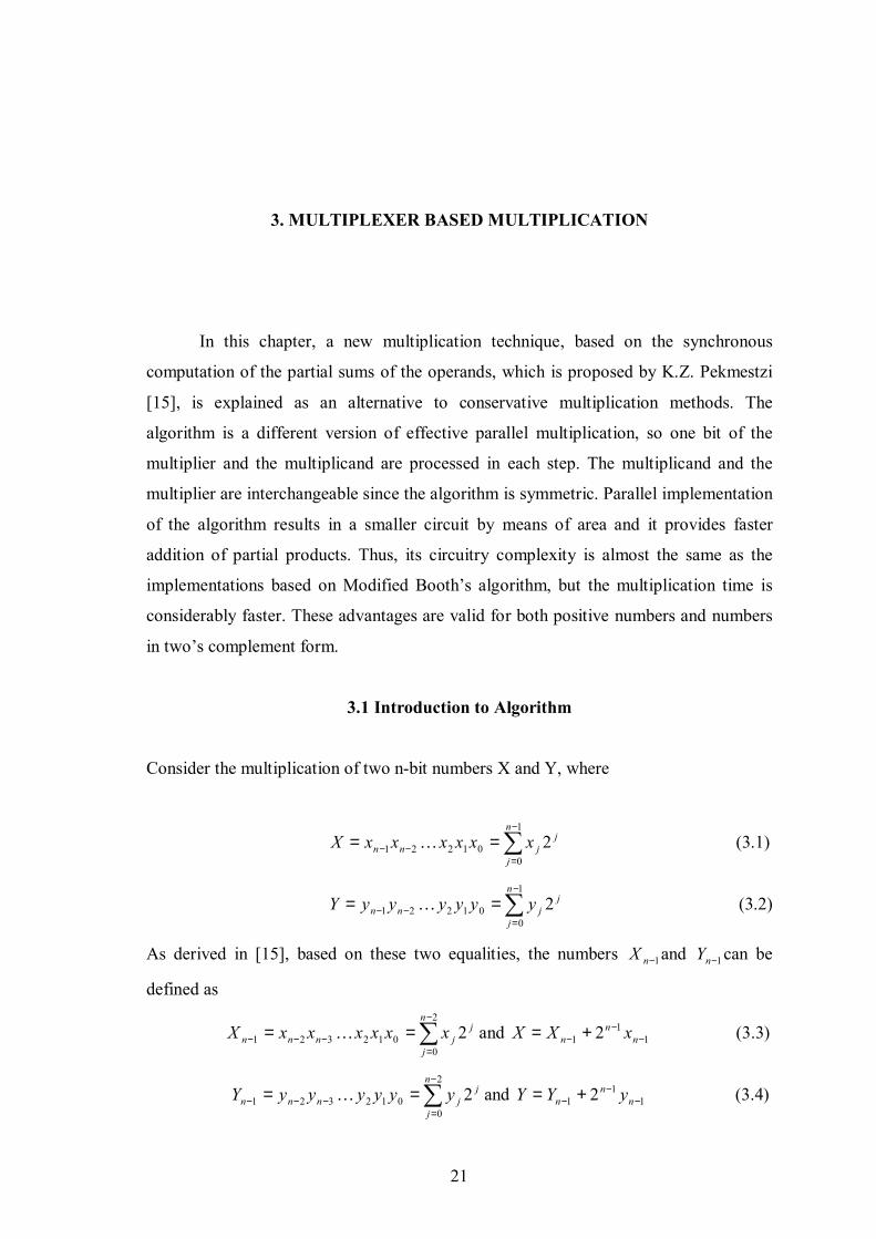
The multiplexer based multiplier array has two different types of cells. The first
type, which is shown in Figure 3.5(a), consists of a 4-to-1 multiplexer and a full-adder.
At the thi row of the array, jx and jy bits are transmitted to )1( in −− first type cells.
In the thj diagonal row of the array, j first type cells and one second type cell exist,
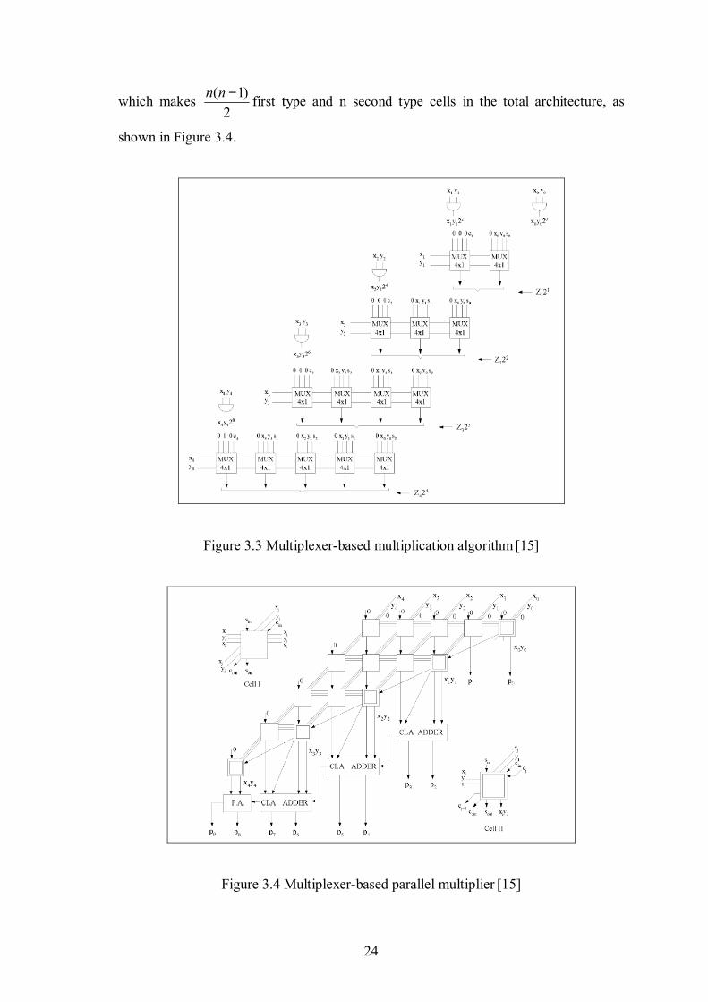
24
which makes 2
)1( −nn first type and n second type cells in the total architecture, as
shown in Figure 3.4.
Figure 3.3 Multiplexer-based multiplication algorithm [15]
Figure 3.4 Multiplexer-based parallel multiplier [15]
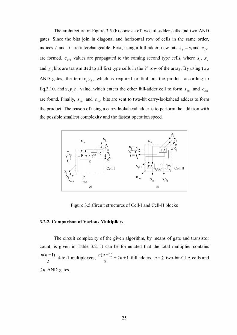
25
The architecture in Figure 3.5 (b) consists of two full-adder cells and two AND
gates. Since the bits join in diagonal and horizontal row of cells in the same order,
indices i and j are interchangeable. First, using a full-adder, new bits ij ss = and 1+jc
are formed. 1+jc values are propagated to the coming second type cells, where ji xs ,
and jy bits are transmitted to all first type cells in the ith row of the array. By using two
AND gates, the term jj yx , which is required to find out the product according to
Eq.3.10, and jjj cyx value, which enters the other full-adder cell to form outs and outc
are found. Finally, outs and outc bits are sent to two-bit carry-lookahead adders to form
the product. The reason of using a carry-lookahead adder is to perform the addition with
the possible smallest complexity and the fastest operation speed.
Figure 3.5 Circuit structures of Cell-I and Cell-II blocks
3.2.2. Comparison of Various Multipliers
The circuit complexity of the given algorithm, by means of gate and transistor
count, is given in Table 3.2. It can be formulated that the total multiplier contains
2)1( −nn 4-to-1 multiplexers, 12
2)1( ++− nnn full adders, 2−n two-bit-CLA cells and
n2 AND-gates.

26
CIRCUIT GATES TRANSISTORS Half Adder 5 10 Full Adder 12 26 2-to-1 MUX 3 6 4-to-1 MUX 5 16 XOR 4 6 2-Bit CLA 23 50
Table 3.2 Number of gates and transistors for various types of circuits
Based on the number of transistors of various circuit types, given in Table 3.2,
the total number of gates and transistors of various multiplier types are presented in
Table 3.3, in order to make a comparison between those types by means of circuit
complexity. It’s noticed that Pekmestzi’s multiplier has almost the same complexity as
the implementations of Modified Booth’s algorithm, and it is much more smaller than
other types.
Type of Multiplier Number of Cells Number of Gates Number of Transistors
Array 2n 213n 230n
Counter Cell 2/)1( +nn )23(13 2 −+ nn )23(30 2 −+ nn
Modified Booth’s Algorithm
Cell A: 2( 1) / 2n + Cell B: ( 1) / 2n +
132310 2 ++ nn 315221 2 ++ nn
MUX Based Multiplier Cell I: ( 1) / 2n n − Cell II: n CLA: n
225.165.8 2 −+ nn 993721 2 −+ nn
Table 3.3 Circuit complexity comparison of various multipliers
Pekmestzi’s multiplier also has the smallest operation delay. The multiplication
time of the structure is equal to FAnT τ)1( += , FAτ being the delay of a full-adder;
under the assumption of carry propagation delay of a two-bit carry-lookahead adder is
also FAτ . This delay is significantly small when compared to the operation delay of the
conventional array multiplier, which is FAnT τ)12( −= . Even though the carry
propagate adders are replaced with carry-lookahead adders in order to perform a faster

27
addition and to shorten the multiplication time, the total delay is found to be
)log( 2 nnFA +τ , which is still slower than that of the structure in Fig. 3.4
Type of Multiplier Operation Time (with FA’s) Operation Time (with CLA’s) Array FAn τ)12( − )log( 2 nnFA +τ
Counter Cell tn )1( + tn )1( +
Modified Booth’s Algorithm 2/3 FAnτ FAFA nn ττ 2log2/ +
MUX Based Multiplier FAn τ)1( + FAn τ)1( +
Table 3.4 Operation time comparison of various multipliers
3.2.3. Modification for Two’s Complement Numbers
The algorithm proposed by Pekmestzi is also applicable for two’s complement
numbers, with a few modifications in the equations. Signed integer numbers X and
Y can be represented as:
∑−
=−
−−− +−==
2
01
101221 22
n
j
jjn
nnn xxxxxxxX K (3.12)
1112 −−
− +−= nnn XxX (3.13)
∑−
=−
−−− +−==
2
01
101221 22
n
j
jjn
nnn yyyyyyyY K (3.14)
1112 −−
− +−= nnn YyY (3.15)
YXP ⋅=
{ } { }111
111 22 −−
−−−
− +−⋅+−= nnn
nnn YyXx
{ } 1111111
1122 22 −−−−−−
−−−
− ++−= nnnnnnn
nnn YXyXYxyx (3.16)
The only difference between Eq.(3.8) and Eq.(3.16) is the sign of the term
11111 −−−−− += nnnnn yXYxZ . All the other terms in the algorithms remain the same but
instead of addition, subtraction operation is needed for 1−nZ in the array. This can be
performed by inverting outS bits of the left boundary cells of the structure given in Fig.
3.4. Since no circuit complexity has been changed, the signed number multiplier yields
the same performance as the positive number multiplier, which is given in Fig. 3.4.

28
4. DESIGN OF DIGITAL BLOCKS
This thesis aims to implement a 64 x 64 – bit multiplier using multiplexer based
multiplication method, in order to check whether the proposed criteria for the algorithm,
explained in Chapter 3, is valid for such a large multiplier and to compare the
architecture with other conventional multiplier types, by means of speed and power
consumption. The whole structure is designed and simulated at 3.3V, 250MHz, using
the environment of Cadence Design Framework AMS 0.35 µm CMOS technology.
Since main components of the multiplier are full-adder and 4-to-1 multiplexer, design
and verification of these elements will be examined in this chapter. Design of AND,
OR, XOR gates are not explained due to the simplicity of their structures, however it’s
worth to note that first design criteria for all the blocks used in the multiplier has been
obtaining minimum possible propagation delay.
4.1 Full Adder Design
Since addition forms the basis of many binary operations, adder circuits are of
great interest in digital design. In order to fulfill the various speed, power and area
requirements of implementations, a wide variety of adder circuits have been proposed in
literature. As the most frequently used block in the overall design is full-adder, now we
turn our attention to build an efficient full-adder, which operates with the possible
minimum delay and power consumption, due to highly dependency of multiplier’s
operation time to the delay of the full-adder, FAτ .
A binary full adder is a three-input and two-output combinational circuit.
Considering that A and B are the input bits to be added, C is the carry input, SUM is the
sum output and CARRY is the carry output, the truth table of the full-adder cell is
shown in Table 4.1.
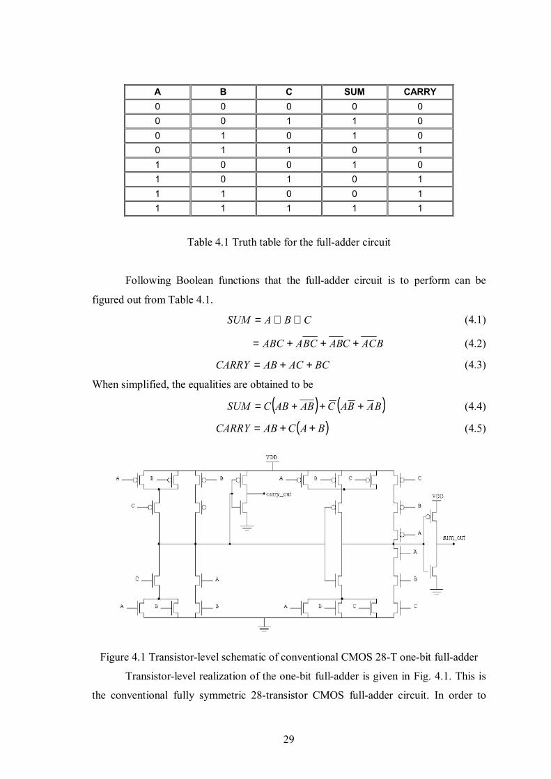
29
A B C SUM CARRY 0 0 0 0 0 0 0 1 1 0 0 1 0 1 0 0 1 1 0 1 1 0 0 1 0 1 0 1 0 1 1 1 0 0 1 1 1 1 1 1
Table 4.1 Truth table for the full-adder circuit
Following Boolean functions that the full-adder circuit is to perform can be
figured out from Table 4.1.
CBASUM ⊕⊕= (4.1)
BACCABBCAABC +++= (4.2)
BCACABCARRY ++= (4.3)
When simplified, the equalities are obtained to be
( ) ( )BABACABABCSUM +++= (4.4)
( )BACABCARRY ++= (4.5)
Figure 4.1 Transistor-level schematic of conventional CMOS 28-T one-bit full-adder
Transistor-level realization of the one-bit full-adder is given in Fig. 4.1. This is
the conventional fully symmetric 28-transistor CMOS full-adder circuit. In order to
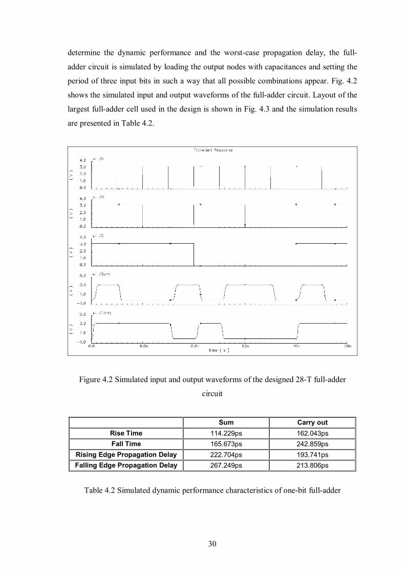
30
determine the dynamic performance and the worst-case propagation delay, the full-
adder circuit is simulated by loading the output nodes with capacitances and setting the
period of three input bits in such a way that all possible combinations appear. Fig. 4.2
shows the simulated input and output waveforms of the full-adder circuit. Layout of the
largest full-adder cell used in the design is shown in Fig. 4.3 and the simulation results
are presented in Table 4.2.
Figure 4.2 Simulated input and output waveforms of the designed 28-T full-adder
circuit
Sum Carry out Rise Time 114.229ps 162.043ps Fall Time 165.673ps 242.859ps
Rising Edge Propagation Delay 222.704ps 193.741ps Falling Edge Propagation Delay 267.249ps 213.806ps
Table 4.2 Simulated dynamic performance characteristics of one-bit full-adder
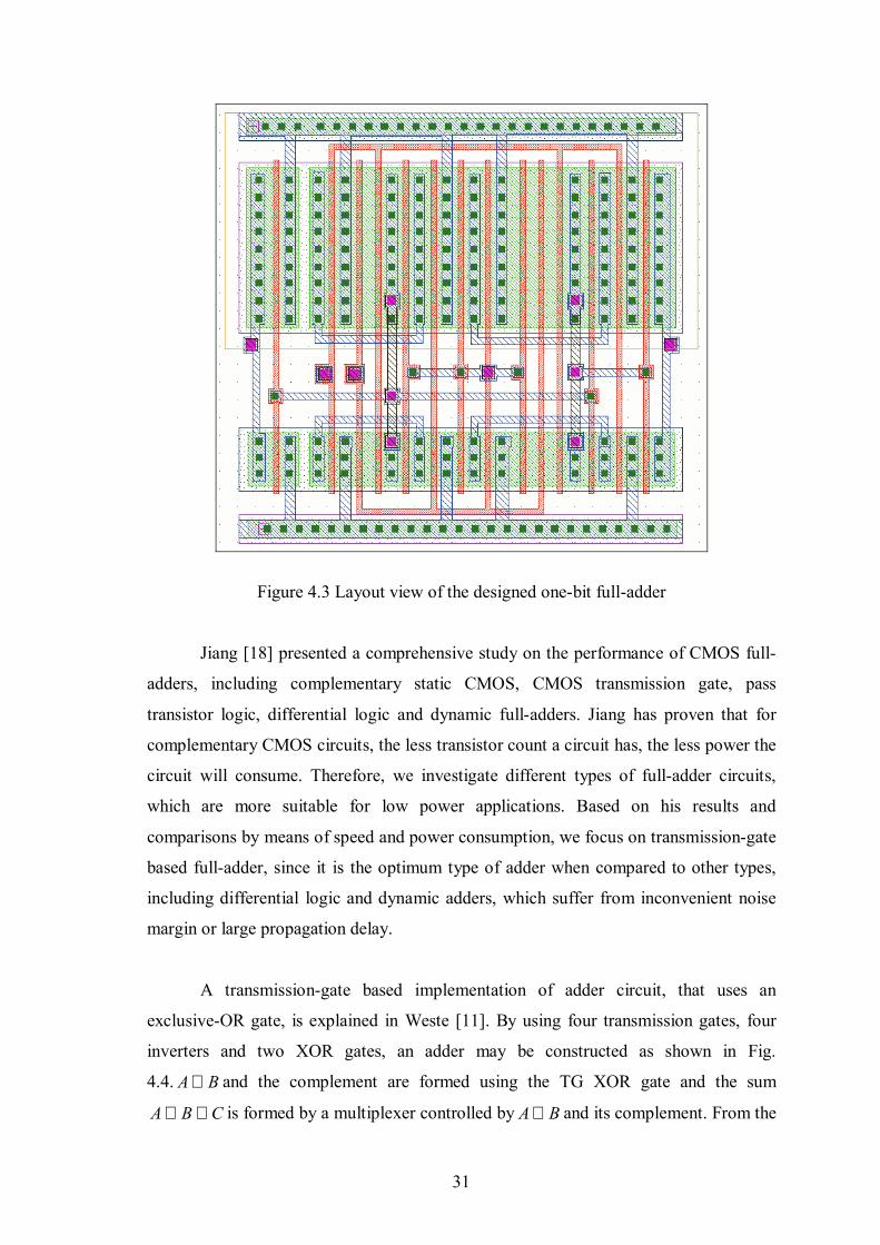
31
Figure 4.3 Layout view of the designed one-bit full-adder
Jiang [18] presented a comprehensive study on the performance of CMOS full-
adders, including complementary static CMOS, CMOS transmission gate, pass
transistor logic, differential logic and dynamic full-adders. Jiang has proven that for
complementary CMOS circuits, the less transistor count a circuit has, the less power the
circuit will consume. Therefore, we investigate different types of full-adder circuits,
which are more suitable for low power applications. Based on his results and
comparisons by means of speed and power consumption, we focus on transmission-gate
based full-adder, since it is the optimum type of adder when compared to other types,
including differential logic and dynamic adders, which suffer from inconvenient noise
margin or large propagation delay.
A transmission-gate based implementation of adder circuit, that uses an
exclusive-OR gate, is explained in Weste [11]. By using four transmission gates, four
inverters and two XOR gates, an adder may be constructed as shown in Fig.
4.4. A B⊕ and the complement are formed using the TG XOR gate and the sum
A B C⊕ ⊕ is formed by a multiplexer controlled by A B⊕ and its complement. From the
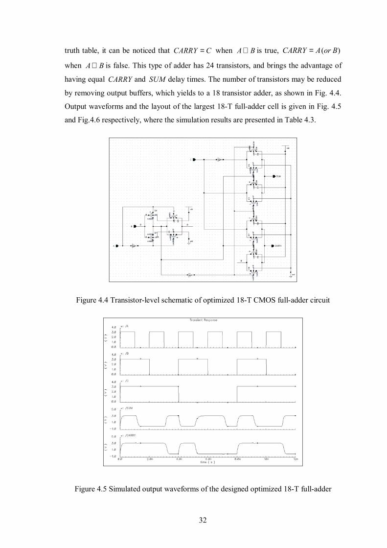
32
truth table, it can be noticed that CARRY C= when A B⊕ is true, ( )CARRY A or B=
when A B⊕ is false. This type of adder has 24 transistors, and brings the advantage of
having equal CARRY and SUM delay times. The number of transistors may be reduced
by removing output buffers, which yields to a 18 transistor adder, as shown in Fig. 4.4.
Output waveforms and the layout of the largest 18-T full-adder cell is given in Fig. 4.5
and Fig.4.6 respectively, where the simulation results are presented in Table 4.3.
Figure 4.4 Transistor-level schematic of optimized 18-T CMOS full-adder circuit
Figure 4.5 Simulated output waveforms of the designed optimized 18-T full-adder

33
Sum Carry Rise Time 53.629ps 40.3943ps Fall Time 69.752ps 96.837ps
Rising Edge Propagation Delay 139.371ps 147.729ps Falling Edge Propagation Delay 179.548ps 186.866ps
Table 4.3 Simulated dynamic performance characteristics of 18-T one-bit full-adder
Figure 4.6 Layout view of the designed 18-T one-bit full-adder
4.2 Multiplexer Design
A multiplexer is a combinational circuit that selects binary information from one
of many input lines and directs the information to a single output line. Selection of a
particular input line is controlled by a set of input variables, called selection –or
control– bits. Generally, there are 2n input lines and n control inputs, whose bit

34
combinations determine which input is selected. Gate-level realization of a single 4-to-1
multiplexer is shown in Fig. 4.7, where each of the four inputs -I0 through I3- is applied
to one input of an AND gate and 0S and 1S are control bits to select a particular AND
gate. The truth table for 4-to-1 multiplexer is given in Table 4.4.
S1 S0 OUT (Y) 0 0 I0 0 1 I1 1 0 I2 1 1 I3
Table 4.4 Truth table for 4-to-1 multiplexer
Figure 4.7 Gate-level schematic of 4-1 multiplexer
Designing an n-to-1 MUX is possible by building a tree of 2-to-1 multiplexers.
Considering that the delay of 2-to-1 MUX is smaller than that of an AND gate, and
using the circuit given in Fig. 4.7 suffers from delay due to three gates (AND-OR gates
and an inverter), it’s more advantageous to use cascaded 2-to1 MUXs. Since we will
use 4-to-1 MUX’s in this design, creating a 2-to-1 MUX tree does not bring any
drawback by means of speed or power dissipation. The transistor-level schematics of a
2-to-1 multiplexer and the cascaded block are given in Fig. 4.8 and Fig. 4.9
respectively. Simulation waveforms of the block are shown in Fig. 4.10 and the

35
simulated results of dynamic performance characteristics of the multiplexer are
presented in Table 4.5.
Figure 4.8 Transistor-level schematic of 2-1 multiplexer
Figure 4.9 Schematic of 4-1 multiplexer
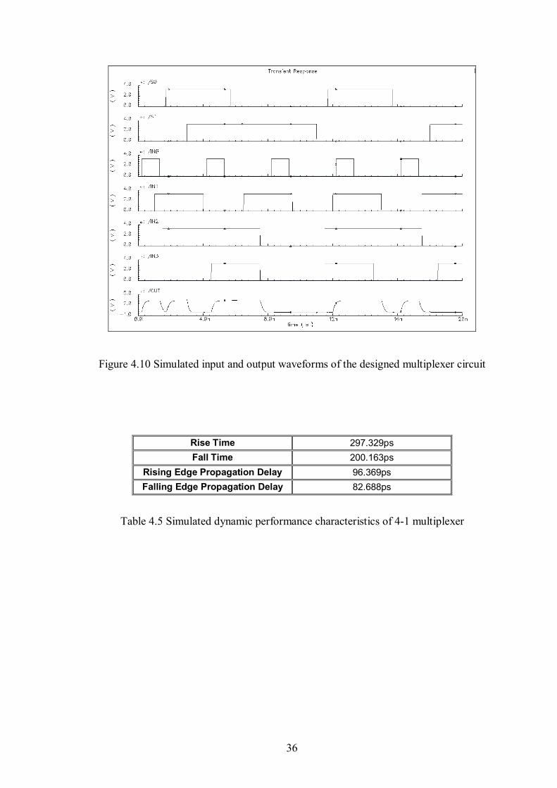
36
Figure 4.10 Simulated input and output waveforms of the designed multiplexer circuit
Rise Time 297.329ps Fall Time 200.163ps
Rising Edge Propagation Delay 96.369ps Falling Edge Propagation Delay 82.688ps
Table 4.5 Simulated dynamic performance characteristics of 4-1 multiplexer
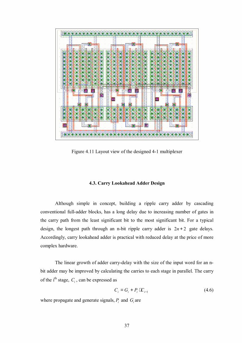
37
Figure 4.11 Layout view of the designed 4-1 multiplexer
4.3. Carry Lookahead Adder Design
Although simple in concept, building a ripple carry adder by cascading
conventional full-adder blocks, has a long delay due to increasing number of gates in
the carry path from the least significant bit to the most significant bit. For a typical
design, the longest path through an n-bit ripple carry adder is 2 2n + gate delays.
Accordingly, carry lookahead adder is practical with reduced delay at the price of more
complex hardware.
The linear growth of adder carry-delay with the size of the input word for an n-
bit adder may be improved by calculating the carries to each stage in parallel. The carry
of the ith stage, iC , can be expressed as
1−⋅+= iiii CPGC (4.6)
where propagate and generate signals, iP and iG are

38
iii BAG ⋅= (4.7)
iii BAP += (4.8)
Expanding this yields,
01211 CPPGPPGPGC iiiiiiii KK++++= −−− (4.9)
Sum is generated by
i i i iS C A B= ⊕ ⊕ (4.10)
For four stages of carry lookahead (CLA), the appropriate terms are
1 1 1 0C G P C= + (4.11)
2 2 2 1 2 1 0C G P G P P G= + + (4.12)
3 3 3 2 3 2 1 3 2 1 0C G P G P P G P P P G= + + + (4.13)
The critical path in the CLA travels in a vertical direction rather than a
horizontal one. Therefore, the delay of CLA is not directly proportional to the size of
the operands n, but to the number of levels used as a tree structure. Thus, the delay is
proportional to the log function of size n. This is evaluated by considering that an adder
with a single level of CLA (four bit words) contains three gate delays in the carry path.
Each additional level of lookahead increases the maximum word size by a factor of
k and adds two additional gate delays. Generally, the number of lookahead levels for an
n-bit adder is logk n where 1k + is the maximum number of inputs per gate. Since a
k -bit group CLA introduces three gate delays per CLA level and there are two
additional gate delays; one for iP and iG and one for the final sum iS , CLA delay ∆ is
( )1 2 log 1 1 2 logCLA k kn n∆ = + − + = (4.14)
This log dependency makes CLA one of the theoretically fastest structures for
addition. In our design, we only need two-bit CLA’s. Schematic view of a two-bit CLA
block is shown in Fig. 4.12. Simulation waveforms of the designed block are given in
Fig. 4.13 where the propagation delay values are presented in Table 4.6. Finally, the
layout of the CLA block is also included, as shown in Fig. 4.14.
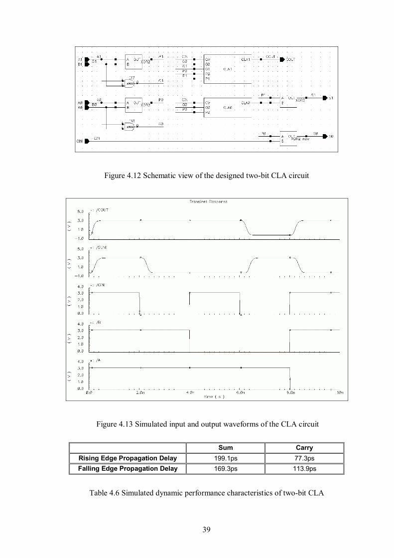
39
Figure 4.12 Schematic view of the designed two-bit CLA circuit
Figure 4.13 Simulated input and output waveforms of the CLA circuit
Sum Carry Rising Edge Propagation Delay 199.1ps 77.3ps Falling Edge Propagation Delay 169.3ps 113.9ps
Table 4.6 Simulated dynamic performance characteristics of two-bit CLA
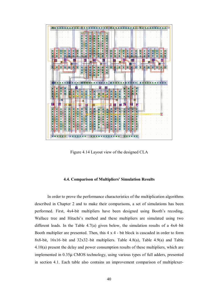
40
Figure 4.14 Layout view of the designed CLA
4.4. Comparison of Multipliers' Simulation Results
In order to prove the performance characteristics of the multiplication algorithms
described in Chapter 2 and to make their comparisons, a set of simulations has been
performed. First, 4x4-bit multipliers have been designed using Booth’s recoding,
Wallace tree and Hitachi’s method and these multipliers are simulated using two
different loads. In the Table 4.7(a) given below, the simulation results of a 4x4–bit
Booth multiplier are presented. Then, this 4 x 4 - bit block is cascaded in order to form
8x8-bit, 16x16–bit and 32x32–bit multipliers. Table 4.8(a), Table 4.9(a) and Table
4.10(a) present the delay and power consumption results of these multipliers, which are
implemented in 0.35µ CMOS technology, using various types of full adders, presented
in section 4.1. Each table also contains an improvement comparison of multiplexer-

41
based multipliers over other types, which are given in Tables 4.7(b), 4.8(b), 4.9(b) and
4.10(b). Simulations are performed at 3.3V supply voltage, with loads of 10fF, 20 Ff,
50fF and 100fF.
Multiplier Type Adder Type Prop. Delay (ns) Power (µW) Load CMOS 28-T 1.41 ns TG 24-T FA 1.29 ns TG 18-T FA 1.22 ns
4 x 4 – bit Booth multiplier
CLA 1.19 ns
~ 265 uW 20 fF
CMOS 28-T 1.60 ns TG 24-T FA 1.46 ns TG 18-T FA 1.37 ns
4 x 4 – bit Booth multiplier
CLA 1.31 ns
~ 1325 uW 100fF
CMOS 28-T 0.995 ns TG 24-T FA 0.967 ns TG 18-T FA 0.903 ns
4 x 4 – bit Wallace tree
CLA 0.881 ns
~ 276 uW 20 fF
CMOS 28-T 1.19 ns TG 24-T FA 1.11 ns TG 18-T FA 1.01 ns
4 x 4 – bit Wallace tree
CLA 0.988 ns
~ 1380 uW 100fF
CMOS 28-T 0.992 ns TG 24-T FA 0.961 ns TG 18-T FA 0.897 ns
4 x 4 – bit Hitachi’s multiplier
CLA 0.866 ns
~ 245 uW 20 fF
CMOS 28-T 1.17 ns TG 24-T FA 1.08 ns TG 18-T FA 0.997 ns
4 x 4 – bit Hitachi’s multiplier
CLA 0.974 ns
~ 1225 uW 100fF
CMOS 28-T 0.998 ns TG 24-T FA 0.956 ns TG 18-T FA 0.867 ns
4 x 4 – bit Multiplexer based multiplier
CLA 0.804 ns
~ 108 uW 20 fF
CMOS 28-T 1.09 ns TG 24-T FA 0.989 ns TG 18-T FA 0.928 ns
4 x 4 – bit Multiplexer based multiplier
CLA 0.912 ns
~ 544 uW 100fF
Table 4.7(a) Performance characteristics of simulated 4 x 4 - bit multiplier blocks

42
Improvement Table of 4 x 4 – bit Multiplexer Based Multipliers Improvement over Adder Type Prop. Delay (ns) Power (µW) Load
CMOS 28-T 29.22 % TG 24-T FA 25.89 % TG 18-T FA 28.93 %
CLA 32.44 %
59.25 % 20 fF
CMOS 28-T 31.88 % TG 24-T FA 32.26 % TG 18-T FA 32.26 %
Booth multiplier
CLA 30.38 %
58.94 % 100fF
CMOS 28-T -0.30 % TG 24-T FA 1.14 % TG 18-T FA 3.99 %
CLA 8.74 %
60.87 % 20 fF
CMOS 28-T 8.40 % TG 24-T FA 10.90 % TG 18-T FA 8.12 %
Wallace tree
CLA 7.69 %
60.58 % 100fF
CMOS 28-T -0.60 % TG 24-T FA 0.52 % TG 18-T FA 3.34 %
CLA 7.16 %
55.92 % 20 fF
CMOS 28-T 6.84 % TG 24-T FA 8.43 % TG 18-T FA 6.92 %
Hitachi’s multiplier
CLA 6.37 %
55.59 % 100fF
Table 4.7(b) Improvement of 4 x 4 – bit multiplexer-based multiplier over other
multiplier types
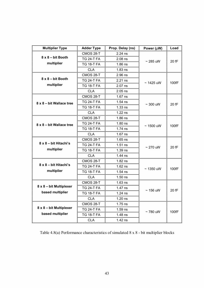
43
Multiplier Type Adder Type Prop. Delay (ns) Power (µW) Load CMOS 28-T 2.24 ns TG 24-T FA 2.08 ns TG 18-T FA 1.86 ns
8 x 8 – bit Booth multiplier
CLA 1.83 ns
~ 285 uW 20 fF
CMOS 28-T 2.96 ns TG 24-T FA 2.21 ns TG 18-T FA 2.07 ns
8 x 8 – bit Booth multiplier
CLA 2.05 ns
~ 1425 uW 100fF
CMOS 28-T 1.67 ns TG 24-T FA 1.54 ns TG 18-T FA 1.33 ns
8 x 8 – bit Wallace tree
CLA 1.22 ns
~ 300 uW 20 fF
CMOS 28-T 1.86 ns TG 24-T FA 1.80 ns TG 18-T FA 1.74 ns
8 x 8 – bit Wallace tree
CLA 1.67 ns
~ 1500 uW 100fF
CMOS 28-T 1.65 ns TG 24-T FA 1.51 ns TG 18-T FA 1.39 ns
8 x 8 – bit Hitachi’s multiplier
CLA 1.44 ns
~ 270 uW 20 fF
CMOS 28-T 1.82 ns TG 24-T FA 1.62 ns TG 18-T FA 1.54 ns
8 x 8 – bit Hitachi’s multiplier
CLA 1.50 ns
~ 1350 uW 100fF
CMOS 28-T 1.63 ns TG 24-T FA 1.47 ns TG 18-T FA 1.24 ns
8 x 8 – bit Multiplexer based multiplier
CLA 1.20 ns
~ 156 uW 20 fF
CMOS 28-T 1.75 ns TG 24-T FA 1.59 ns TG 18-T FA 1.48 ns
8 x 8 – bit Multiplexer based multiplier
CLA 1.42 ns
~ 780 uW 100fF
Table 4.8(a) Performance characteristics of simulated 8 x 8 - bit multiplier blocks
44
Improvement Table of 8 x 8 – bit Multiplexer Based Multipliers Improvement over Adder Type Prop. Delay (ns) Power (µW) Load
CMOS 28-T 27.23 % TG 24-T FA 29.33 % TG 18-T FA 33.33 %
CLA 34.43 %
45.26 % 20 fF
CMOS 28-T 40.88 % TG 24-T FA 28.05 % TG 18-T FA 28.50 %
Booth multiplier
CLA 30.73 %
45.26 % 100fF
CMOS 28-T 2.40 % TG 24-T FA 4.55 % TG 18-T FA 6.77 %
CLA 1.64 %
48.00 % 20 fF
CMOS 28-T 5.91 % TG 24-T FA 11.67 % TG 18-T FA 14.94 %
Wallace tree
CLA 14.97 %
48.00 % 100fF
CMOS 28-T 1.21 % TG 24-T FA 2.65 % TG 18-T FA 10.79 %
CLA 16.67 %
42.22 % 20 fF
CMOS 28-T 3.85 % TG 24-T FA 1.85 % TG 18-T FA 3.90 %
Hitachi’s multiplier
CLA 5.33 %
42.22 % 100fF
Table 4.8(b) Improvement of 8 x 8 – bit multiplexer-based multiplier over other
multiplier types

45
Multiplier Type Adder Type Prop. Delay (ns) Power (µW) Load CMOS 28-T 2.76 ns TG 24-T FA 2.58 ns TG 18-T FA 2.42 ns
16 x 16 – bit Booth multiplier
CLA 2.26 ns
~ 350 uW 20 fF
CMOS 28-T 3.08 ns TG 24-T FA 2.89 ns TG 18-T FA 2.72 ns
16 x 16 – bit Booth multiplier
CLA 2.68 ns
~ 875 uW 50 fF
CMOS 28-T 2.24 ns TG 24-T FA 2.10 ns TG 18-T FA 2.06 ns
16 x 16 – bit Wallace tree
CLA 1.91 ns
~ 400 uW 20 fF
CMOS 28-T 2.57 ns TG 24-T FA 2.44 ns TG 18-T FA 2.33 ns
16 x 16 – bit Wallace tree
CLA 2.19 ns
~ 1000 uW 50 fF
CMOS 28-T 2.14 ns TG 24-T FA 1.99 ns TG 18-T FA 1.94 ns
16 x 16 – bit Hitachi’s multiplier
CLA 1.89 ns
~ 325 uW 20 fF
CMOS 28-T 2.26 ns TG 24-T FA 2.18 ns TG 18-T FA 1.98 ns
16 x 16 – bit Hitachi’s multiplier
CLA 1.90 ns
~ 813 uW 50 fF
CMOS 28-T 2.23 ns TG 24-T FA 2.07 ns TG 18-T FA 1.92 ns
16 x 16 – bit Multiplexer based multiplier
CLA 1.89 ns
~ 250 uW 20 fF
CMOS 28-T 2.67 ns TG 24-T FA 2.43 ns TG 18-T FA 2.14 ns
16 x 16 – bit Multiplexer based multiplier
CLA 2.10 ns
~ 625 uW 50 fF
Table 4.9(a) Performance characteristics of simulated 16 x 16 - bit multiplier blocks
46
Improvement Table of 16 x 16 – bit Multiplexer Based Multipliers Improvement over Adder Type Prop. Delay (ns) Power (µW) Load
CMOS 28-T 19.20 % TG 24-T FA 19.77 % TG 18-T FA 20.66 %
CLA 16.37 %
28.57 % 20 fF
CMOS 28-T 13.31 % TG 24-T FA 15.92 % TG 18-T FA 21.32 %
Booth multiplier
CLA 21.64 %
28.57 % 50 fF
CMOS 28-T 0.45 % TG 24-T FA 1.43 % TG 18-T FA 6.80 %
CLA 1.05 %
37.50 % 20 fF
CMOS 28-T -3.89 % TG 24-T FA 0.41 % TG 18-T FA 8.15 %
Wallace tree
CLA 4.11 %
37.50 % 50 fF
CMOS 28-T -4.21 % TG 24-T FA -4.02 % TG 18-T FA 1.03 %
CLA 0.00 %
23.08 % 20 fF
CMOS 28-T -18.14 % TG 24-T FA -11.47 % TG 18-T FA -8.08 %
Hitachi’s multiplier
CLA -10.53 %
23.12 % 50 fF
Table 4.9(b) Improvement of 16 x 16 – bit multiplexer-based multiplier over
other multiplier types
47
Multiplier Type Adder Type Prop. Delay (ns) Power (µW) Load CMOS 28-T 12.26 ns TG 24-T FA 11.48 ns TG 18-T FA 10.82 ns
32 x 32 – bit Booth multiplier
CLA 10.71 ns
~ 800 uW
CMOS 28-T 10.02 ns TG 24-T FA 9.81 ns TG 18-T FA 9.14 ns
32 x 32 – bit Wallace tree
CLA 9.53 ns
~ 750 uW
CMOS 28-T 3.43 ns TG 24-T FA 3.38 ns TG 18-T FA 3.24 ns
32 x 32 – bit Hitachi’s multiplier
CLA 3.69 ns
~ 1000 uW
CMOS 28-T 9.72 ns TG 24-T FA 9.04 ns TG 18-T FA 8.64 ns
32 x 32 – bit Multiplexer based multiplier
CLA 8.76 ns
~ 500 uW
25 fF
Table 4.10(a) Performance characteristics of simulated 32 x 32 - bit multiplier blocks
Improvement Table of 32 x 32 – bit Multiplexer Based Multipliers Improvement over Circuit Type Prop. Delay Power Cons. Load
CMOS 28-T 20.72 % TG 24-T FA 21.25 % TG 18-T FA 20.15 %
Booth’s multiplier
CLA 18.21 %
37.5 %
CMOS 28-T 2.99 % TG 24-T FA 7.85 % TG 18-T FA 5.47 %
Wallace tree
CLA 8.08 %
33.33 %
CMOS 28-T -183.38 % TG 24-T FA -167.46 % TG 18-T FA -166.67 %
Hitachi’s multiplier
CLA -137.40 %
50 %
25 pF
Table 4.10(b) Improvement of 32 x 32 – bit multiplexer-based multiplier over
other multiplier types
48
After examining the simulation results of the multiplier blocks, which are
presented in tables above, it’s not possible to say that one type of adder has
continuously better performance over other adder types. For example, according to its
architecture and logarithmic delay-dependency property, a CLA block is expected to
show better performance than other static adders, especially by means of speed.
However, it is observed that the performance of a multiplier depends on not only the
design criteria of the components that form the block, but also the structural alignment
of those components, which may create a different critical path than expected. Thus, in
some cases a multiplier, designed using static adders (i.e. TG based 18-T adder) has a
better propagation delay than the one designed with CLA. Furthermore, using only CLA
blocks in the multiplier brings a disadvantage; instability at the output, especially in
larger multipliers. That’s why, based on the performance characteristics, it’s decided to
use both CMOS conventional 28-T and the optimized 18-T adders for the FA blocks in
the multiplier structure. In order to form signal integrity and output symmetry, 28-T FA
is used in columns consisting of fewer sub-blocks where 18-T FA is preferred for long
component chains and critical paths. Moreover, among the same type of adders,
transistor dimensions also differ in order to improve the propagation delay of the
multiplier. Layouts of digital blocks, presented in previous sections, belong to the
largest circuits used in the overall design. It is worth to mention the increment in the
propagation delay of the circuits as the size of the multiplied numbers get larger.
Unfortunately, after 16-bit multiplication, there has been an unexpected rapid reduction
in the speed of the multiplexer-based multiplier. Although it still has speed
improvement over Booth and Wallace types, Hitachi’s multiplier is faster at large
number-of- bit multiplications. However, we proceed to implement a 64 x 64 – bit
multiplexer-based multiplier, since our only design criteria is not speed. Moreover, the
obtained results are still comparably satisfactory and efficient, though not as good as
Hitachi’s results.
4.5. Design of 64-bit x 64-bit Multiplier Block
Based on the architecture of Fig. 3.4, the 64 x 64–bit multiplier is designed after
various iterations, like adder and transistor dimension optimizations explained above.

49
When the block is simulated at 3.3V, its operation time is found to be 12.8ns. Core
layout of the multiplier is approximately 21.5mm2. Besides, the worst-case propagation
delay of the 32 x 32 – bit multiplier block, which is designed for fabrication, is found to
be 8.2ns. This block occupies a silicon area of about 4.08mm2. Below, schematic and
layout views of the multiplier blocks are given from Fig.4.15 to Fig.4.20.
Figure 4.15 Schematic view of the Cell-I Block
Figure 4.16 Layout view of the Cell-I Block
Figure 4.17 Schematic view of the Cell-II Block
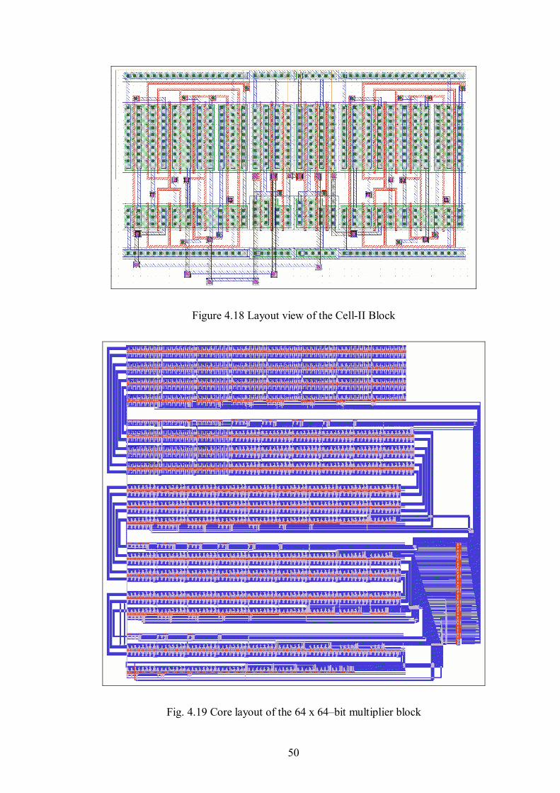
50
Figure 4.18 Layout view of the Cell-II Block
Fig. 4.19 Core layout of the 64 x 64–bit multiplier block
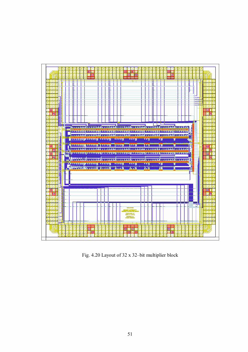
51
Fig. 4.20 Layout of 32 x 32–bit multiplier block
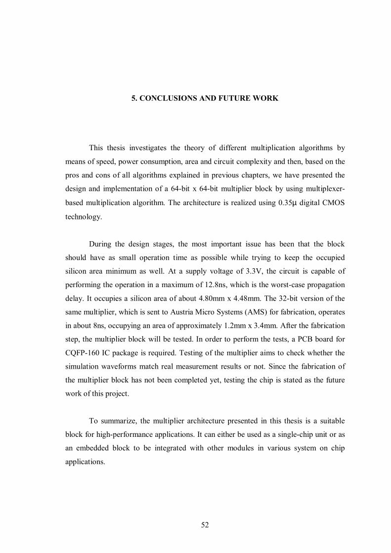
52
5. CONCLUSIONS AND FUTURE WORK
This thesis investigates the theory of different multiplication algorithms by
means of speed, power consumption, area and circuit complexity and then, based on the
pros and cons of all algorithms explained in previous chapters, we have presented the
design and implementation of a 64-bit x 64-bit multiplier block by using multiplexer-
based multiplication algorithm. The architecture is realized using 0.35µ digital CMOS
technology.
During the design stages, the most important issue has been that the block
should have as small operation time as possible while trying to keep the occupied
silicon area minimum as well. At a supply voltage of 3.3V, the circuit is capable of
performing the operation in a maximum of 12.8ns, which is the worst-case propagation
delay. It occupies a silicon area of about 4.80mm x 4.48mm. The 32-bit version of the
same multiplier, which is sent to Austria Micro Systems (AMS) for fabrication, operates
in about 8ns, occupying an area of approximately 1.2mm x 3.4mm. After the fabrication
step, the multiplier block will be tested. In order to perform the tests, a PCB board for
CQFP-160 IC package is required. Testing of the multiplier aims to check whether the
simulation waveforms match real measurement results or not. Since the fabrication of
the multiplier block has not been completed yet, testing the chip is stated as the future
work of this project.
To summarize, the multiplier architecture presented in this thesis is a suitable
block for high-performance applications. It can either be used as a single-chip unit or as
an embedded block to be integrated with other modules in various system on chip
applications.

53
6. REFERENCES
[1] M. S. Elrabaa, I. S. Abu-Khater and M. I. Elmasry, Advanced Low-Power
Digital Circuit Techniques, Kluwer Academic Publishers, 2000.
[2] K. Roy and S. C. Prasad, Low-Power CMOS VLSI Circuit Design, John Wiley &
Sons, 1999.
[3] A. P. Chandrakasan and R. W. Brodersen, Low-Power Digital CMOS Design,
Kluwer Academic Publishers, 1995.
[4] D. A. Pucknell and K. Eshraghian, Basic VLSI Design, Upper Saddle River:
Prentice Hall, 1994.
[5] A. Bellaouar and M. I. Elmasry, Low-Power Digital VLSI Design Circuits and
Systems, Kluwer Academic Publishers, 1997.
[6] W. Wolf, Modern VLSI Design Systems on Silicon, Upper Saddle River:
Prentice Hall, 1998.
[7] J. B. Kuo and J. H. Lou, Low Voltage CMOS VLSI Circuits, John Wiley & Sons,
1999.
[8] S. S. Rofail and K. S. Yeo, Low-Voltage Low-Power Digital BiCMOS Circuits,
Upper Saddle River: Prentice Hall, 2000.
[9] B. Parhami, Computer Arithmetic Algorithms and Hardware Designs, Oxford
University Press, 2000.
[10] A. Chandrakasan, W. J. Bowhill and F. Fox, Design of High Performance
Microprocessor Circuits, IEEE Press, 2001.

54
[11] N. H. E. Weste and K. Eshraghian, Principles of CMOS VLSI Design A System
Perspective, Second Edition, Massachusetts: Addison-Wesley, 1992.
[12] S. Kang and Y. Leblebici, “CMOS Digital Integrated Circuits Analysis and
Design”, McGraw Hill, 1996.
[13] N. Ohkubo, M. Suzuki, T. Shinbo, T. Yamanaka, A. Shimizu, K. Sasaki and Y.
Nakagome, “A 4.4ns CMOS 54 x 54-bit Multiplier Using Pass Transistor
Multiplexer”, IEEE Journal of Solid-State Circuits, vol.30, no. 3, pp.252-257,
March, 1995.
[14] D. W. Kim and D. K. Jeong, “A 32 x 32 Self-Timed Multiplier with Early
Completion”, Proceedings of the Second IEEE Asia Pacific Conference, 1999.
[15] K. Z. Pekmestzi, “Multiplexer-Based Array Multipliers”, IEEE Transactions on
Computers, vol. 48, no. 1, pp.15-23, Jan. 1999.
[16] A. Inoue, R. Ohe, S. Kashiwakura, S. Mitari, T. Tsuru, T. Izawa and G. Goto,
“A 4.1ns Compact 54 x 54–bit Multiplier Using Sign Select Booth Encoders”,
IEEE International Solid State Circuits Conference, Digest of Papers, San
Francisco, 1997.
[17] A. R. Attarha, M. Nourani and M. Zakeri, “High Performance Low-Power
Signed Multiplier”, International Conference of Engineering Education, 1999.
[18] Y. Jiang, “Design and Implementation of Low-Power ASIC Components”,
Ph.D. Thesis, University of Texas at Dallas, Dept. of Computer Science, Texas,
2001.
[19] P. C. H. Meier, “Analysis and Design of Low Power Digital Multipliers”, Ph.D.
Thesis, Carnegie Mellon University, Dept. of Electrical and Computer
Engineering, Pittsburgh, Pennsylvania, 1999.
[20] S. Hong, “Performance Driven VLSI System Design for Low Energy Wireless
Communications”, Ph.D. Thesis, University of Michigan, Dept. of Electrical &
Electronics Engineering, Michigan, 2000.

55
[21] A. Y. Chitari, “VLSI Architecture For A 16–bit Multiply-Accumulator (MAC)
operating in multiplication time”, M.Sc. Thesis, Texas A&M University, Dept.
of Electrical & Electronics Engineering, Kingsville, 2000.
[22] K. R. Chada, “Design and Delay Analysis of a Multiplexer based Array
Multiplier”, M.Sc. Thesis, Texas A&M University, Dept. of Electrical &
Electronics Engineering, Kingsville, 2001.
53
6. REFERENCES
[1] M. S. Elrabaa, I. S. Abu-Khater and M. I. Elmasry, Advanced Low-Power
Digital Circuit Techniques, Kluwer Academic Publishers, 2000.
[2] K. Roy and S. C. Prasad, Low-Power CMOS VLSI Circuit Design, John Wiley &
Sons, 1999.
[3] A. P. Chandrakasan and R. W. Brodersen, Low-Power Digital CMOS Design,
Kluwer Academic Publishers, 1995.
[4] D. A. Pucknell and K. Eshraghian, Basic VLSI Design, Upper Saddle River:
Prentice Hall, 1994.
[5] A. Bellaouar and M. I. Elmasry, Low-Power Digital VLSI Design Circuits and
Systems, Kluwer Academic Publishers, 1997.
[6] W. Wolf, Modern VLSI Design Systems on Silicon, Upper Saddle River:
Prentice Hall, 1998.
[7] J. B. Kuo and J. H. Lou, Low Voltage CMOS VLSI Circuits, John Wiley & Sons,
1999.
[8] S. S. Rofail and K. S. Yeo, Low-Voltage Low-Power Digital BiCMOS Circuits,
Upper Saddle River: Prentice Hall, 2000.
[9] B. Parhami, Computer Arithmetic Algorithms and Hardware Designs, Oxford
University Press, 2000.
[10] A. Chandrakasan, W. J. Bowhill and F. Fox, Design of High Performance
Microprocessor Circuits, IEEE Press, 2001.

54
[11] N. H. E. Weste and K. Eshraghian, Principles of CMOS VLSI Design A System
Perspective, Second Edition, Massachusetts: Addison-Wesley, 1992.
[12] S. Kang and Y. Leblebici, “CMOS Digital Integrated Circuits Analysis and
Design”, McGraw Hill, 1996.
[13] N. Ohkubo, M. Suzuki, T. Shinbo, T. Yamanaka, A. Shimizu, K. Sasaki and Y.
Nakagome, “A 4.4ns CMOS 54 x 54-bit Multiplier Using Pass Transistor
Multiplexer”, IEEE Journal of Solid-State Circuits, vol.30, no. 3, pp.252-257,
March, 1995.
[14] D. W. Kim and D. K. Jeong, “A 32 x 32 Self-Timed Multiplier with Early
Completion”, Proceedings of the Second IEEE Asia Pacific Conference, 1999.
[15] K. Z. Pekmestzi, “Multiplexer-Based Array Multipliers”, IEEE Transactions on
Computers, vol. 48, no. 1, pp.15-23, Jan. 1999.
[16] A. Inoue, R. Ohe, S. Kashiwakura, S. Mitari, T. Tsuru, T. Izawa and G. Goto,
“A 4.1ns Compact 54 x 54–bit Multiplier Using Sign Select Booth Encoders”,
IEEE International Solid State Circuits Conference, Digest of Papers, San
Francisco, 1997.
[17] A. R. Attarha, M. Nourani and M. Zakeri, “High Performance Low-Power
Signed Multiplier”, International Conference of Engineering Education, 1999.
[18] Y. Jiang, “Design and Implementation of Low-Power ASIC Components”,
Ph.D. Thesis, University of Texas at Dallas, Dept. of Computer Science, Texas,
2001.
[19] P. C. H. Meier, “Analysis and Design of Low Power Digital Multipliers”, Ph.D.
Thesis, Carnegie Mellon University, Dept. of Electrical and Computer
Engineering, Pittsburgh, Pennsylvania, 1999.
[20] S. Hong, “Performance Driven VLSI System Design for Low Energy Wireless
Communications”, Ph.D. Thesis, University of Michigan, Dept. of Electrical &
Electronics Engineering, Michigan, 2000.
55
[21] A. Y. Chitari, “VLSI Architecture For A 16–bit Multiply-Accumulator (MAC)
operating in multiplication time”, M.Sc. Thesis, Texas A&M University, Dept.
of Electrical & Electronics Engineering, Kingsville, 2000.
[22] K. R. Chada, “Design and Delay Analysis of a Multiplexer based Array
Multiplier”, M.Sc. Thesis, Texas A&M University, Dept. of Electrical &
Electronics Engineering, Kingsville, 2001.