
Design and Performance Analysis of Low Power … · Design and Performance Analysis of Low Power...
7
Page 203 Design and Performance Analysis of Low Power High Speed Full Adder Circuits Using 22NM Technology D.Venkatachari M.Tech Student, Department of ECE, VIZAG Institute of Technology, Visakhapatnam, A.P, India. Balaji Valli Assistant Professor, Department of ECE, VIZAG Institute of Technology, Visakhapatnam, A.P, India. Abstract: This paper gives the performance of full adder design in terms of area, power and delay in different logic styles. Full adder design achieves low power in Single Gate MOSFET logic compared to all other topologies such as Basic CMOS, Pass Transistor, Double Gate MOSFET and GDI techniques but it make use of less number of transistors comparatively GDI. SGMOSFET occupies the less area comparatively all other logic styles. The simulations of the proposed full adder have been performed using Tanner EDA Tool version 13.0. All the proposed design simulations are carried out at 90nm, 45nm and 22nm technology for various inputs like supply voltage, temperature and frequency. Simulated outcome using state-of-art simulation tool shows power and speed comparison of different full adder designs also presented. Keywords: CMOS, GDI, Single Gate Mosfet, Double Gate Mosfet, State-of-art, Predictive Technology. 1. INTRODUCTION: To reduce the size of chip, the complexity in the circuits has increased drastically, because of that the power dissipation and performance of the circuit are being affected. So, there is concern towards circuits design in low power VLSI design to reduce the chip area and power dissipation. There are two types of power dissipations in MOSFET, namely static power and dynamic power dissipations. In Static power dissipation sub-threshold leakage, gate direct tunneling leakage, reverse-biased junction leakage and gate induced drain leakage shows the major effect in various scaling parameters. In Dynamic power dissipation switching and short circuit power will have the effect. The static and dynamic power dissipations are calculated theoretically from the equations shown in 1 and 2 respectively. P s =I cc ∗V DD …………….. (1) P D = 1 2 C L (∆V 0 ) 2 f....…….... (2) Where, I cc = Sum of leakage current V DD = Supply voltage C L = Load capacitance ∆V 0 = Logic voltage swing f= Frequency of switching Power delay product (PDP=P AVG *T) is a parameter we used for comparison between various circuits to estimate the optimised results which can be operated at different frequency regions. A full adder is the base in digital circuits employed for performing arithmetical and logical operations, compressors, comparators and parity checkers. In present world of VLSI system applications such as specific DSP architecture, Systolic array design, microprocessors, FIR Filters, perform fundamental operations. Full adder is a core element that determines the overall performance of arithmetic circuit. In this paper, we designed improved full adder which operates in 22nm scaling technology using Single Gate Mosfet logic. This paper summarizes as follows , Section 2 Power Consumption in VLSI Circuits, Section 3 describes the topologies of the implemented low power full adders. Section 4 represents the proposed circuit designs.
Transcript of Design and Performance Analysis of Low Power … · Design and Performance Analysis of Low Power...

Page 203
Design and Performance Analysis of Low Power High Speed Full
Adder Circuits Using 22NM Technology D.Venkatachari
M.Tech Student,
Department of ECE,
VIZAG Institute of Technology,
Visakhapatnam, A.P, India.
Balaji Valli
Assistant Professor,
Department of ECE,
VIZAG Institute of Technology,
Visakhapatnam, A.P, India.
Abstract:
This paper gives the performance of full adder design
in terms of area, power and delay in different logic
styles. Full adder design achieves low power in Single
Gate MOSFET logic compared to all other topologies
such as Basic CMOS, Pass Transistor, Double Gate
MOSFET and GDI techniques but it make use of less
number of transistors comparatively GDI.
SGMOSFET occupies the less area comparatively all
other logic styles. The simulations of the proposed full
adder have been performed using Tanner EDA Tool
version 13.0. All the proposed design simulations are
carried out at 90nm, 45nm and 22nm technology for
various inputs like supply voltage, temperature and
frequency. Simulated outcome using state-of-art
simulation tool shows power and speed comparison of
different full adder designs also presented.
Keywords:
CMOS, GDI, Single Gate Mosfet, Double Gate
Mosfet, State-of-art, Predictive Technology.
1. INTRODUCTION:
To reduce the size of chip, the complexity in the
circuits has increased drastically, because of that the
power dissipation and performance of the circuit are
being affected. So, there is concern towards circuits
design in low power VLSI design to reduce the chip
area and power dissipation. There are two types of
power dissipations in MOSFET, namely static power
and dynamic power dissipations. In Static power
dissipation sub-threshold leakage, gate direct tunneling
leakage, reverse-biased junction leakage and gate
induced drain leakage shows the major effect in
various scaling parameters. In Dynamic power
dissipation switching and short circuit power will have
the effect. The static and dynamic power dissipations
are calculated theoretically from the equations shown
in 1 and 2 respectively.
Ps = Icc ∗ VDD…………….. (1)
PD =1
2CL(∆V0)
2f....…….... (2)
Where, Icc = Sum of leakage current
VDD= Supply voltage
CL= Load capacitance
∆V0 = Logic voltage swing
f= Frequency of switching
Power delay product (PDP=PAVG*T) is a parameter we
used for comparison between various circuits to
estimate the optimised results which can be operated at
different frequency regions. A full adder is the base in
digital circuits employed for performing arithmetical
and logical operations, compressors, comparators and
parity checkers. In present world of VLSI system
applications such as specific DSP architecture, Systolic
array design, microprocessors, FIR Filters, perform
fundamental operations. Full adder is a core element
that determines the overall performance of arithmetic
circuit. In this paper, we designed improved full adder
which operates in 22nm scaling technology using
Single Gate Mosfet logic. This paper summarizes as
follows , Section 2 Power Consumption in VLSI
Circuits, Section 3 describes the topologies of the
implemented low power full adders. Section 4
represents the proposed circuit designs.

Page 204
The simulation results are shown and discussed from
the observations in waveforms and power delay
product values of different circuits presented in section
5 the conclusions in section 6 followed references in
Section 7.
2. POWER CONSUMPTION IN VLSI CIRCUITS
2.1 Why low-power design?
i. Battery lifetime (especially for portable devices)
ii. Reliability
2.2. Low Power Strategies:
• OS level : Partitioning, Power down
• Software level : Regularity, Locality and
Concurrency ( Compiler technology for low power,
instruction scheduling )
• Architecture level : Pipelining, Redundancy and Data
Encoding ( ISA, architectural design, memory
hierarchy, HW extensions, etc )
• Circuit/logic level : Logic styles, Transistor sizing
and Energy recovery ( Logic families, conditional
clocking, adiabatic circuits, asynchronous design )
• Technology level : Threshold reductions and multi-
threshold devices etc...
2.3 Main components of power consumption in
digital VLSI circuits.
2.3.1. Switching component: consumed in charging
and discharging of the circuit capacitances during
transistor switching.
2.3.2. Short-circuit component: Created by short-
circuit current flowing from supply voltage to ground
during transistor switching.
2.2.3. Static power component: Existence of static
and leakage currents in stable state of circuit cause this
component of power consumption.
The first two components are referred to as dynamic
power, since power is consumed dynamically while
the circuit is changing states. Dynamic power accounts
for the majority of the total power consumption in
digital VLSI circuits
The average power dissipation for a CMOS circuit is
given by
Pavg = Pdynamic+ Pshort circuit + Pstatic ………..(1)
= Vdd .fclk .Σ(Vi swing .Ci load . αi ) + Vdd.ΣIi sc
+Vdd.
The challenge that has been faced by VLSI designers
is to find effective techniques and their efficient
applications to get minimum power dissipation without
any compromise on their performance evaluation
parameters. Thus, the design of low power circuits
with improved performance is a major concern of
modern VLSI designs. The combination of certain
logic styles and low power modules with low leakage
circuit topologies may greatly reduce the limitations of
deep-sub-micro-meter technologies. At the system
level, in synchronous implementation of
microprocessors, adder cells are the basic modules in a
variety of arithmetic units such as arithmetic logical
units, ripple carry adders , multipliers etc.
Now a days, as growing applications, speed and
portability are the major concerns of any smart device
it demands small-size, low-power high throughput
circuitry. So, sub circuits of any VLSI chip needs high
speed operation along with low-power consumption.
So that logic circuits are designed using pass transistor
logic techniques. [1]. It reduces the number of MOS
transistors used in circuit, but it suffers with a major
problem that output voltage levels is no longer same as
the input voltage level. Each transistor in series has a
lower voltage at its output than at its input.
Low power is not only needed for portable
applications but also to reduce the power of high
performance systems. With large integration density
and improved speed of operation, systems with high
clock frequencies are emerging. These systems are
using high speed processors and associated circuits
which increase the power consumption[2]. The cost
associated with cooling, packaging and fans required
by these systems to remove the heat generated because
of power consumption is increasing significantly.
Page 205
3. PREVIOUS WORK
3.1. CMOS Full Adder
Starting with basic CMOS full adder circuit which
consists of 28 transistors as shown in figure 1[3], with
less delay and high speed it also has good voltage
swing, so the circuit’s performance will be good but its
power dissipation is more because the transistor’s
count is high so the area occupied by the circuit is
more[4]. This CMOS logic is the basic logic operation
of any circuit. It has PMOS in the pull up mode and
NMOS in the pull down mode, so reducing the
transistors count in the logic circuit is very difficult.
Figure 1. Basic CMOS full adder circuit
3.2. GDI:
The basic architecture of the 2:1 MUX using GDI
method is shown in fig 2.[5] In this configuration we
have connected PMOS and NMOS gate along with a
SEL line ‘A’, as in MUX. As we know that PMOS
works on ACTIVE LOW and NMOS works on
ACTIVE HIGH. So, when the SELECT input is low
(0) then the PMOS get activated, and show the input
‘B’ in the output and due to low input (0) the NMOS
stands idle, as it is activated in high input. Same for the
case, while the G input is high (1) then the NMOS get
activated, and show the input ‘C’ at the output. Thus
this circuitry behaves as a 2-input MUX using ‘A’ as
SEL line, and shows the favourable output as
2:1MUX. Now it's implemented the low power full
adder circuit with the help of 2T MUX, made by GDI
technique. It require total 6 numbers of 2T MUX
having same characteristics to design a 12T full
adder[6].
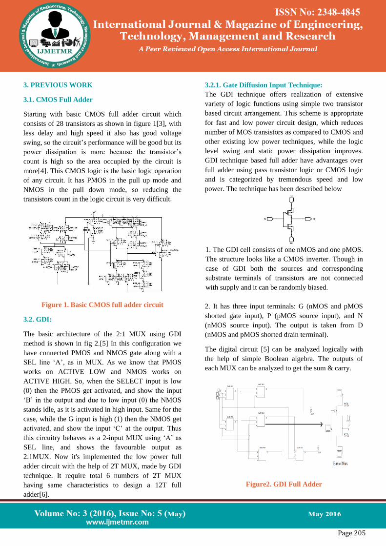
3.2.1. Gate Diffusion Input Technique:
The GDI technique offers realization of extensive
variety of logic functions using simple two transistor
based circuit arrangement. This scheme is appropriate
for fast and low power circuit design, which reduces
number of MOS transistors as compared to CMOS and
other existing low power techniques, while the logic
level swing and static power dissipation improves.
GDI technique based full adder have advantages over
full adder using pass transistor logic or CMOS logic
and is categorized by tremendous speed and low
power. The technique has been described below
1. The GDI cell consists of one nMOS and one pMOS.
The structure looks like a CMOS inverter. Though in
case of GDI both the sources and corresponding
substrate terminals of transistors are not connected
with supply and it can be randomly biased.
2. It has three input terminals: G (nMOS and pMOS
shorted gate input), P (pMOS source input), and N
(nMOS source input). The output is taken from D
(nMOS and pMOS shorted drain terminal).
The digital circuit [5] can be analyzed logically with
the help of simple Boolean algebra. The outputs of
each MUX can be analyzed to get the sum & carry.
Figure2. GDI Full Adder

Page 206
Figure 3. 12-Transistor adder.
3.2.2. Logic Analysis:
The digital circuit shown in fig 3.5 can be analyzed
logically with the help of simple Boolean algebra. The
outputs of each MUX can be analyzed to get the sum
and carry.
MUX 1=(BA1+CA)
MUX 2 =(CA1+BA)
MUX 3=[(CA1+BA)C1+(BA1+CA)C]
=ABC1+A1BC+AC
=ABC1+A1BC+AC(B+B1)
=ABC1+A1BC+ABC+AB1C
=ABC1+ABC+A1BC+ ABC+ AB1C+ABC
=AB(C+C1)+BC(A+A1)+AC(B+B1)
=AB+BC+AC=Cout
MUX 4=A1B+(A1B+AC)B
MUX 5=(CA1+BA)B1+AB
MUX 6=[A1B+(A1B+AC)B]C1+[(CA1+BA)B1+AB]C
=AB1C1+A1BC1+ABC=SUM
4. PROPOSED FA CIRCUITS using 22nm
TECHNOLOGY:
4.1. Single gate MOSFET Full Adder
In order to reduce the transistors count in full adder, a
circuit is designed by using single gate MOSFET
consists of 10 transistors as shown in figure 4. Here in
this logic VDD supply voltage is not required as the
outputs sum and carry will be produced from the three
applied inputs[7]. The main drawback in it is that its
voltage swing is poor. It requires high input voltages to
obtain the outputs, because of which the power
dissipation of the circuit will be more and also
XNOR/XOR sub-circuit doesn’t provide stable output
for applied zero inputs, because of which the logic of
the circuit may differ for low transitions.
Figure 4. Single gate MOSFET full adder circuit
4.2. Double gate MOSFET Full Adder
To overcome the drawbacks in Single gate MOSFET
i.e., to increase the output voltage swing in Single gate
MOSFET a double gate MOSFET is designed by
connecting two single gate transistors back to back in
such a way that sources and drains of two single gate
MOSFET transistors are connected respectively as
shown in figure 5.This circuit has 4 pairs of NMOS
and 6 pairs of PMOS. The logic and analysis is similar
to Single gate MOSFET except voltage swing. But the
draw back in this case is that it consumes more power
when compared to single gate MOSFET. Generally
size of PMOS is doubled than size of NMOS but in
Double gate MOSFET W/L ratio is maintained as 1:1
for all transistors, because of which there is leakage in
PMOS transistors[7]. The W/L ratio is maintained so
as to attain sufficient output voltage swing.
Figure 5. Double gate MOSFET full adder circuit

Page 207
5. SIMULATION RESULTS AND ANALYSIS:
In this Basic CMOS 22nm technology we apply supply
voltage as 0.9V for better voltage swing. Here we
maintain W/L ratio as 2:1. As shown in fig 6 and GDI
logic is shown in fig 7. In this single gate full adder we
cannot get the output logic when VDD=0.9V as shown
in the fig 8. So that we increase input voltage up to
1.5V at that voltage we got the output it was shown in
fig 9. Double gate MOSFET output logic is similar to
the single gate MOSFET output logic as in fig 10 and
11.
Figure 6. Basic CMOS full adder simulation results
in 22nm
Figure 7. GDI
Figure 8. Single gate MOSFET simulation result in
22nm when VDD=0.9V
Figure 9. Single gate MOSFET simulation results in
22nm when VDD=1.5V
Figure 10. Double gate MOSFET simulation result
in 22nm when VDD=0.9V

Page 208
Figure 11. Double gate MOSFET simulation results
in 22nm when VDD=1.5V
The average power dissipation in different nano meter
scales of full adder circuits is shown in table 1. From
the table, in 90nm and 22nm technology the modified
full adder consumes less power. Coming to 45nm
single gate MOSFET consumes less power but as
mentioned in section II, “it doesn’t give strong zero at
carry at transition zero”, as shown in fig 8. So, the
proposed full adder has less power dissipation
with good performance compared to remaining
circuits. Similarly, the power delay product analysis is
done in table 2, the results shows that the proposed
circuit had the best optimized results. In table 3, the
results are taken by operating the full adder circuits
with different frequencies and the minimum required
supply voltages for operating with good voltage
swings are tabulated. In fig 10 and fig 11 the power
dissipation and power delay product of the circuits are
shown respectively. Fig 12 shows the comparison of
required voltage to run the circuit with good voltage
swing with respect to frequency. Fig 14 shows the area
comparison with different technologies. Fig 15 shows
the Layouts of GDI.
Figure 12. Power Dissipation analysis
Table 1. Power dissipation
Table 2. Power delay product
Table 3. Area in 22nm scaling technology with
lambda=0.1um
Figure 13. Power delay product analysis
0
2
4
6
90 nm
45 nm
22 nm 0
2
4
6
90nm
45nm
22nm
S.No FULL
ADDER
90nm 45nm 22nm
1 Basic
CMOS
1.132 5.16 0.0362
2 Single gate
MOSFET
0.1854 0.787 0.0362
3 Double
gate
MOSFET
1.1124 0.63 1.19
4 GDI 0.33 0.115 0.0239

Page 209
Figure14. Area Comparison of different models in
22nm technology
Figure 15. Full Adder Layout using GDI
6. CONCLUSION:
The performance parameters such as power, area and
speed are evaluated for full adder in various nanoscale
technologies. The simulation results show that as we
go on scaling there is drastic decrease in power
consumption of full adder. It not only achieves the low
power but also operate at high speed. Post-Layout
simulations show that the full design occupies the less
space in 22nm technology compared to other
nanoscale technologies. Single gate Mosfet got low
area and low power compared with other logics. The
full adder designs are best suitable for low power high-
speed applications.
REFERENCES:
[1] Jaume Segura, Charles F. Hawkins CMOS
electronics: how it works, how it fails, Wiley-IEEE,
2004, p age 132
[2] International Journal of Computer Applications
(0975 – 8887 " Analysis of Various Full-Adder
Circuits in Cadence" Page 30-37
[3] Yano, K, et al, "A 3.8 ns CMOS 16*16b multiplier
using complementary pass transistor logic", IEEE J.
Solid State Circuits, Vol 25, p388-395, April 1990
[4] ”An improved low power high speed full adder
design with 28nm for extended region of operation”,
Deepak K Jena, ICECCE 2014. LSI Design”PHI
Publications by Douglas A.Pucknell, Kamran
Eshragian
[5] Arkadiy Morgenshtein, Alexander Fish, and Israel
A. Wagner, "Gate- Diffusion Input (GDI): A Power-
Efficient Method for Digital Combinatorial Circuits",
IEEE Transaction on VLSI Systems, Vol. 10
[6] A.Bazzazi and B. Eskafi, "Design and
Implementation of Full Adder Cell with the GDI
Technique Based on 0.18μm CMOS Technology",
International MultiConference of Engineers and
Computer Scientists (IMES) Vol II, March 17 - 19,
2010, Hong Kong
[7] “ Design of Full Adder circuit using Double Gate
MOSFET”, JagdeepKaurSahani, Shiwani Singh,2015.
0
200
400
600
800
1000
1200
1400
1600
1800
2000
22nm
XxY