Design and optimization of thermo-mechanical … and optimization of thermo-mechanical reliability...
11
Design and optimization of thermo-mechanical reliability in wafer level packaging X.J. Fan a,b, * , B. Varia a , Q. Han b a Department of Mechanical Engineering, Lamar University, P.O. Box 10028, Beaumont, TX 77710, USA b College of Civil Engineering and Transportation, South China University of Technology, Guangzhou, PR China article info Article history: Received 4 July 2009 Received in revised form 16 November 2009 Available online 29 January 2010 abstract In this paper, a variety of wafer level packaging (WLP) structures, including both fan-in and fan-out WLPs, are investigated for solder joint thermo-mechanical reliability performance, from a structural design point of view. The effects of redistribution layer (RDL), bump structural design/material selection, poly- mer-cored ball application, and PCB design/material selection are studied. The investigation focuses on four different WLP technologies: standard WLP (ball on I/O WLP), ball on polymer WLP without under bump metallurgy (UBM) layer, ball on polymer WLP with UBM layer, and encapsulated copper post WLP. Ball on I/O WLP, in which solder balls are directly attached to the metal pads on silicon wafer, is used as a benchmark for the analysis. 3-D finite element modeling is performed to investigate the effects of WLP structures, UBM layer, polymer film material properties (in ball on polymer WLP), and encapsu- lated epoxy material properties (in copper post WLP). Both ball on polymer and copper post WLPs have shown great reliability improvement in thermal cycling. For ball on polymer WLP structures, polymer film between silicon and solder balls creates a ‘cushion’ effect to reduce the stresses in solder joints. Such cushion effect can be achieved either by an extremely compliant film or a ‘hard’ film with a large coef- ficient of thermal expansion. Encapsulated copper post WLP shows the best thermo-mechanical perfor- mance among the four WLP structures. Furthermore, for a fan-out WLP, it has been found that the critical solder balls are the outermost solder balls under die-area, where the maximum thermal mismatch takes place. In a fan-out WLP package, chip size, other than package size, determines the limit of solder joint reliability. This paper also discusses the polymer-cored solder ball applications to enhance thermo-mechanical reliability of solder joints. Finally, both experimental and finite element analysis have demonstrated that making corner balls non-electrically connected can greatly improve the WLP thermo- mechanical reliability. Ó 2009 Elsevier Ltd. All rights reserved. 1. Introduction Wafer level packaging (WLP) is one of the fast growing seg- ments in semiconductor packaging industry due to the rapid ad- vances in integrated circuit (IC) fabrication and the demands of a growing market for faster, lighter, smaller, yet less expensive elec- tronic products with high performance and low-cost packaging [1– 3]. WLPs are mainly used for low pin-count and small die-size applications, such as analog devices, power management devices, image sensors, integrated passives, and memory devices. More WLPs appear in handheld devices such as cellular phones. WLP is an advanced packaging technology, in which the dies or packages are fabricated and tested at the wafer level before singulation. By performing batch wafer level testing and packaging, the processing costs can be brought down significantly. Many IC makers are incor- porating WLP into their designs, and migrating from traditional wirebond interconnection to WLP solutions. As such, a paradigm shift to wafer level packaging is apparent. It is well understood that solder joint thermo-mechanical reli- ability performance become a critical concern of WLPs with larger die packages [3,4]. The ability of solder joint to survive the required thermal cycle testing has limited the WLPs to the products having relatively small die-sizes and a small number of I/O. The intrinsic difference in the coefficient of thermal expansion (CTE) between silicon (2.6 ppm/°C) and PCB (16 ppm/°C) determines that the solder ball thermal cycling fatigue performance is limited by die- size. However, there has been a demand for WLP development with larger die, finer pitch and higher functionality applications. Consequently, there is an urgent need to develop new WLP tech- nologies to address this concern of meeting reliability requirement for large array WLPs. A variety of WLP technologies have been developed in recent years to improve the thermo-mechanical reliability performance for large array WLPs. Standard WLP, which is similar to a typical flip chip technology, has evolved with the incorporation 0026-2714/$ - see front matter Ó 2009 Elsevier Ltd. All rights reserved. doi:10.1016/j.microrel.2009.11.010 * Corresponding author. Address: Department of Mechanical Engineering, Lamar University, P.O. Box 10028, Beaumont, TX 77710, USA. Tel.: +1 409 880 7792; fax: +1 409 880 8121. E-mail address: [email protected] (X.J. Fan). Microelectronics Reliability 50 (2010) 536–546 Contents lists available at ScienceDirect Microelectronics Reliability journal homepage: www.elsevier.com/locate/microrel
-
Upload
truonghuong -
Category
Documents
-
view
230 -
download
4
Transcript of Design and optimization of thermo-mechanical … and optimization of thermo-mechanical reliability...
Microelectronics Reliability 50 (2010) 536–546
Contents lists available at ScienceDirect
Microelectronics Reliability
journal homepage: www.elsevier .com/locate /microrel
Design and optimization of thermo-mechanical reliability in wafer level packaging
X.J. Fan a,b,*, B. Varia a, Q. Han b
a Department of Mechanical Engineering, Lamar University, P.O. Box 10028, Beaumont, TX 77710, USAb College of Civil Engineering and Transportation, South China University of Technology, Guangzhou, PR China
a r t i c l e i n f o a b s t r a c t
Article history:Received 4 July 2009Received in revised form 16 November 2009Available online 29 January 2010
0026-2714/$ - see front matter � 2009 Elsevier Ltd. Adoi:10.1016/j.microrel.2009.11.010
* Corresponding author. Address: Department of MUniversity, P.O. Box 10028, Beaumont, TX 77710, USA+1 409 880 8121.
E-mail address: [email protected] (X.J. Fan).
In this paper, a variety of wafer level packaging (WLP) structures, including both fan-in and fan-out WLPs,are investigated for solder joint thermo-mechanical reliability performance, from a structural designpoint of view. The effects of redistribution layer (RDL), bump structural design/material selection, poly-mer-cored ball application, and PCB design/material selection are studied. The investigation focuses onfour different WLP technologies: standard WLP (ball on I/O WLP), ball on polymer WLP without underbump metallurgy (UBM) layer, ball on polymer WLP with UBM layer, and encapsulated copper postWLP. Ball on I/O WLP, in which solder balls are directly attached to the metal pads on silicon wafer, isused as a benchmark for the analysis. 3-D finite element modeling is performed to investigate the effectsof WLP structures, UBM layer, polymer film material properties (in ball on polymer WLP), and encapsu-lated epoxy material properties (in copper post WLP). Both ball on polymer and copper post WLPs haveshown great reliability improvement in thermal cycling. For ball on polymer WLP structures, polymerfilm between silicon and solder balls creates a ‘cushion’ effect to reduce the stresses in solder joints. Suchcushion effect can be achieved either by an extremely compliant film or a ‘hard’ film with a large coef-ficient of thermal expansion. Encapsulated copper post WLP shows the best thermo-mechanical perfor-mance among the four WLP structures. Furthermore, for a fan-out WLP, it has been found that the criticalsolder balls are the outermost solder balls under die-area, where the maximum thermal mismatch takesplace. In a fan-out WLP package, chip size, other than package size, determines the limit of solderjoint reliability. This paper also discusses the polymer-cored solder ball applications to enhancethermo-mechanical reliability of solder joints. Finally, both experimental and finite element analysis havedemonstrated that making corner balls non-electrically connected can greatly improve the WLP thermo-mechanical reliability.
� 2009 Elsevier Ltd. All rights reserved.
1. Introduction
Wafer level packaging (WLP) is one of the fast growing seg-ments in semiconductor packaging industry due to the rapid ad-vances in integrated circuit (IC) fabrication and the demands of agrowing market for faster, lighter, smaller, yet less expensive elec-tronic products with high performance and low-cost packaging [1–3]. WLPs are mainly used for low pin-count and small die-sizeapplications, such as analog devices, power management devices,image sensors, integrated passives, and memory devices. MoreWLPs appear in handheld devices such as cellular phones. WLP isan advanced packaging technology, in which the dies or packagesare fabricated and tested at the wafer level before singulation. Byperforming batch wafer level testing and packaging, the processingcosts can be brought down significantly. Many IC makers are incor-
ll rights reserved.
echanical Engineering, Lamar. Tel.: +1 409 880 7792; fax:
porating WLP into their designs, and migrating from traditionalwirebond interconnection to WLP solutions. As such, a paradigmshift to wafer level packaging is apparent.
It is well understood that solder joint thermo-mechanical reli-ability performance become a critical concern of WLPs with largerdie packages [3,4]. The ability of solder joint to survive the requiredthermal cycle testing has limited the WLPs to the products havingrelatively small die-sizes and a small number of I/O. The intrinsicdifference in the coefficient of thermal expansion (CTE) betweensilicon (�2.6 ppm/�C) and PCB (�16 ppm/�C) determines that thesolder ball thermal cycling fatigue performance is limited by die-size. However, there has been a demand for WLP developmentwith larger die, finer pitch and higher functionality applications.Consequently, there is an urgent need to develop new WLP tech-nologies to address this concern of meeting reliability requirementfor large array WLPs.
A variety of WLP technologies have been developed in recentyears to improve the thermo-mechanical reliability performancefor large array WLPs. Standard WLP, which is similar to atypical flip chip technology, has evolved with the incorporation
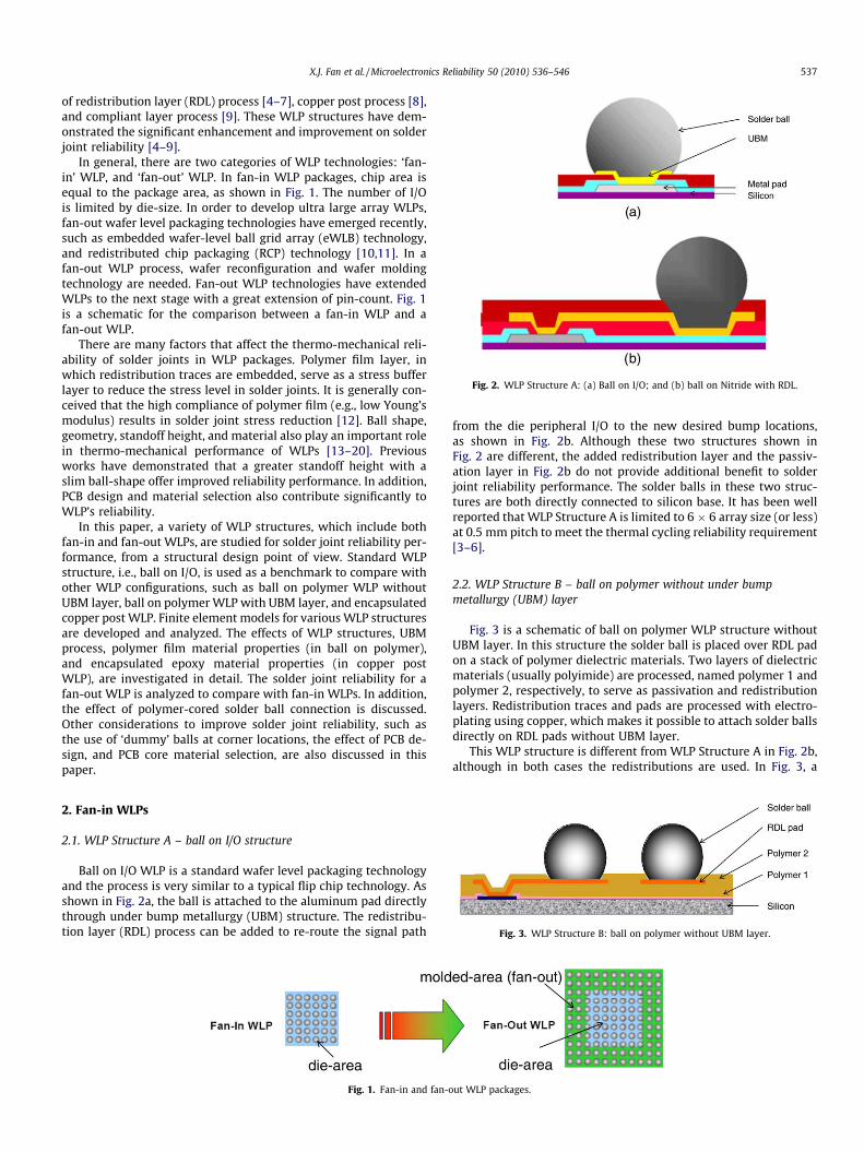
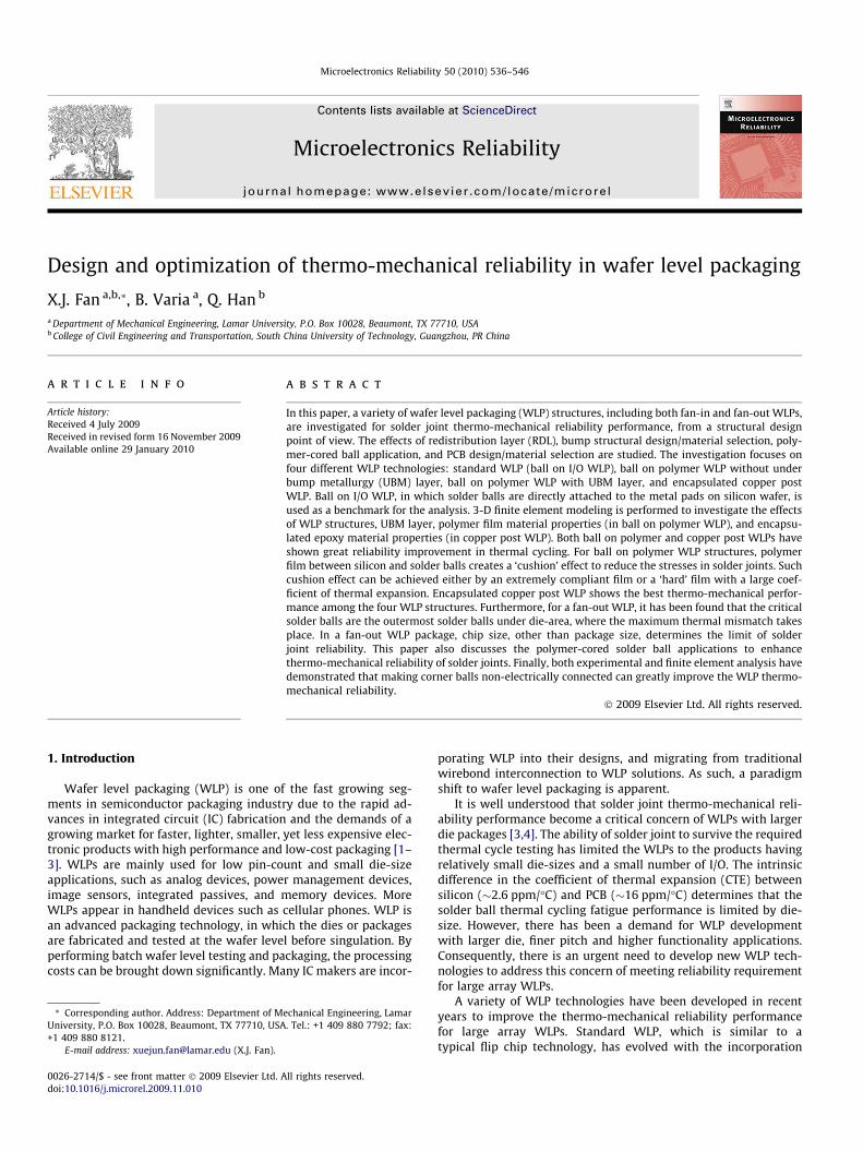
Fig. 2. WLP Structure A: (a) Ball on I/O; and (b) ball on Nitride with RDL.
X.J. Fan et al. / Microelectronics Reliability 50 (2010) 536–546 537
of redistribution layer (RDL) process [4–7], copper post process [8],and compliant layer process [9]. These WLP structures have dem-onstrated the significant enhancement and improvement on solderjoint reliability [4–9].
In general, there are two categories of WLP technologies: ‘fan-in’ WLP, and ‘fan-out’ WLP. In fan-in WLP packages, chip area isequal to the package area, as shown in Fig. 1. The number of I/Ois limited by die-size. In order to develop ultra large array WLPs,fan-out wafer level packaging technologies have emerged recently,such as embedded wafer-level ball grid array (eWLB) technology,and redistributed chip packaging (RCP) technology [10,11]. In afan-out WLP process, wafer reconfiguration and wafer moldingtechnology are needed. Fan-out WLP technologies have extendedWLPs to the next stage with a great extension of pin-count. Fig. 1is a schematic for the comparison between a fan-in WLP and afan-out WLP.
There are many factors that affect the thermo-mechanical reli-ability of solder joints in WLP packages. Polymer film layer, inwhich redistribution traces are embedded, serve as a stress bufferlayer to reduce the stress level in solder joints. It is generally con-ceived that the high compliance of polymer film (e.g., low Young’smodulus) results in solder joint stress reduction [12]. Ball shape,geometry, standoff height, and material also play an important rolein thermo-mechanical performance of WLPs [13–20]. Previousworks have demonstrated that a greater standoff height with aslim ball-shape offer improved reliability performance. In addition,PCB design and material selection also contribute significantly toWLP’s reliability.
In this paper, a variety of WLP structures, which include bothfan-in and fan-out WLPs, are studied for solder joint reliability per-formance, from a structural design point of view. Standard WLPstructure, i.e., ball on I/O, is used as a benchmark to compare withother WLP configurations, such as ball on polymer WLP withoutUBM layer, ball on polymer WLP with UBM layer, and encapsulatedcopper post WLP. Finite element models for various WLP structuresare developed and analyzed. The effects of WLP structures, UBMprocess, polymer film material properties (in ball on polymer),and encapsulated epoxy material properties (in copper postWLP), are investigated in detail. The solder joint reliability for afan-out WLP is analyzed to compare with fan-in WLPs. In addition,the effect of polymer-cored solder ball connection is discussed.Other considerations to improve solder joint reliability, such asthe use of ‘dummy’ balls at corner locations, the effect of PCB de-sign, and PCB core material selection, are also discussed in thispaper.
Fig. 3. WLP Structure B: ball on polymer without UBM layer.
2. Fan-in WLPs
2.1. WLP Structure A – ball on I/O structure
Ball on I/O WLP is a standard wafer level packaging technologyand the process is very similar to a typical flip chip technology. Asshown in Fig. 2a, the ball is attached to the aluminum pad directlythrough under bump metallurgy (UBM) structure. The redistribu-tion layer (RDL) process can be added to re-route the signal path
Fig. 1. Fan-in and fan-o
from the die peripheral I/O to the new desired bump locations,as shown in Fig. 2b. Although these two structures shown inFig. 2 are different, the added redistribution layer and the passiv-ation layer in Fig. 2b do not provide additional benefit to solderjoint reliability performance. The solder balls in these two struc-tures are both directly connected to silicon base. It has been wellreported that WLP Structure A is limited to 6 � 6 array size (or less)at 0.5 mm pitch to meet the thermal cycling reliability requirement[3–6].
2.2. WLP Structure B – ball on polymer without under bumpmetallurgy (UBM) layer
Fig. 3 is a schematic of ball on polymer WLP structure withoutUBM layer. In this structure the solder ball is placed over RDL padon a stack of polymer dielectric materials. Two layers of dielectricmaterials (usually polyimide) are processed, named polymer 1 andpolymer 2, respectively, to serve as passivation and redistributionlayers. Redistribution traces and pads are processed with electro-plating using copper, which makes it possible to attach solder ballsdirectly on RDL pads without UBM layer.
This WLP structure is different from WLP Structure A in Fig. 2b,although in both cases the redistributions are used. In Fig. 3, a
ut WLP packages.
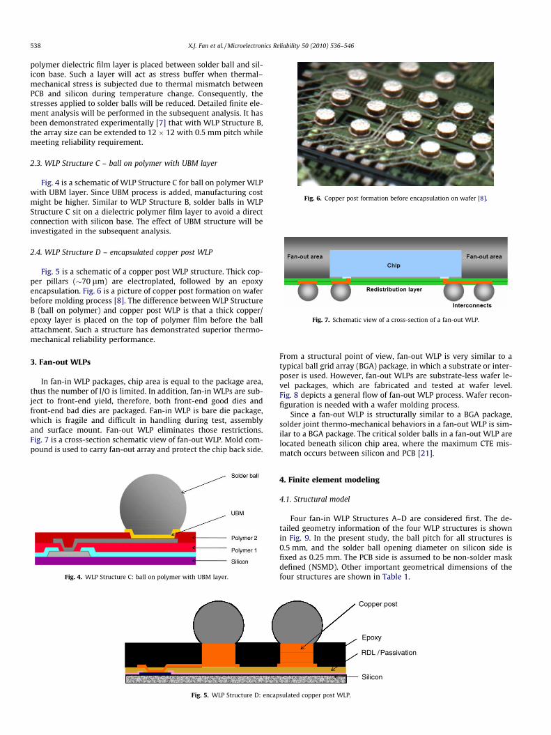
Fig. 6. Copper post formation before encapsulation on wafer [8].
Fig. 7. Schematic view of a cross-section of a fan-out WLP.
538 X.J. Fan et al. / Microelectronics Reliability 50 (2010) 536–546
polymer dielectric film layer is placed between solder ball and sil-icon base. Such a layer will act as stress buffer when thermal–mechanical stress is subjected due to thermal mismatch betweenPCB and silicon during temperature change. Consequently, thestresses applied to solder balls will be reduced. Detailed finite ele-ment analysis will be performed in the subsequent analysis. It hasbeen demonstrated experimentally [7] that with WLP Structure B,the array size can be extended to 12 � 12 with 0.5 mm pitch whilemeeting reliability requirement.
2.3. WLP Structure C – ball on polymer with UBM layer
Fig. 4 is a schematic of WLP Structure C for ball on polymer WLPwith UBM layer. Since UBM process is added, manufacturing costmight be higher. Similar to WLP Structure B, solder balls in WLPStructure C sit on a dielectric polymer film layer to avoid a directconnection with silicon base. The effect of UBM structure will beinvestigated in the subsequent analysis.
2.4. WLP Structure D – encapsulated copper post WLP
Fig. 5 is a schematic of a copper post WLP structure. Thick cop-per pillars (�70 lm) are electroplated, followed by an epoxyencapsulation. Fig. 6 is a picture of copper post formation on waferbefore molding process [8]. The difference between WLP StructureB (ball on polymer) and copper post WLP is that a thick copper/epoxy layer is placed on the top of polymer film before the ballattachment. Such a structure has demonstrated superior thermo-mechanical reliability performance.
3. Fan-out WLPs
In fan-in WLP packages, chip area is equal to the package area,thus the number of I/O is limited. In addition, fan-in WLPs are sub-ject to front-end yield, therefore, both front-end good dies andfront-end bad dies are packaged. Fan-in WLP is bare die package,which is fragile and difficult in handling during test, assemblyand surface mount. Fan-out WLP eliminates those restrictions.Fig. 7 is a cross-section schematic view of fan-out WLP. Mold com-pound is used to carry fan-out array and protect the chip back side.
Fig. 4. WLP Structure C: ball on polymer with UBM layer.
Fig. 5. WLP Structure D: encap
From a structural point of view, fan-out WLP is very similar to atypical ball grid array (BGA) package, in which a substrate or inter-poser is used. However, fan-out WLPs are substrate-less wafer le-vel packages, which are fabricated and tested at wafer level.Fig. 8 depicts a general flow of fan-out WLP process. Wafer recon-figuration is needed with a wafer molding process.
Since a fan-out WLP is structurally similar to a BGA package,solder joint thermo-mechanical behaviors in a fan-out WLP is sim-ilar to a BGA package. The critical solder balls in a fan-out WLP arelocated beneath silicon chip area, where the maximum CTE mis-match occurs between silicon and PCB [21].
4. Finite element modeling
4.1. Structural model
Four fan-in WLP Structures A–D are considered first. The de-tailed geometry information of the four WLP structures is shownin Fig. 9. In the present study, the ball pitch for all structures is0.5 mm, and the solder ball opening diameter on silicon side isfixed as 0.25 mm. The PCB side is assumed to be non-solder maskdefined (NSMD). Other important geometrical dimensions of thefour structures are shown in Table 1.
Copper post
Epoxy
RDL /Passivation
Silicon
sulated copper post WLP.
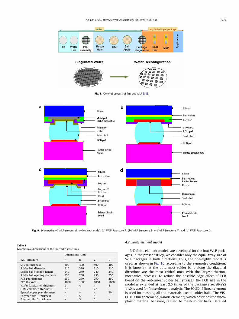
Fig. 8. General process of fan-out WLP [10].
Silicon
Metal padRDL / passivationMetal padRDL / passivation
PolymideUBMPolymideUBM
Solder ball
PCB padPCB pad
P i t d i itPrinted circuit b dboard
Silicon
Passivation
P l 1
Passivation
Polymer 1
Polymer 2
RDL pad
y
RDL pad
Solder ball
PCB padp
Printed circuit boardPrinted circuit board
Silicon
P i i
Silicon
Passivation
Polymer 1
Polymer 2RDL pad
UBM
S ld b llSolder ball
PCB pad
Printed circuitPrinted circuit boardboard
Silicon
Passivation /Passivation /RedistributionRedistribution
EpoxyEpoxy
Copper postCopper post
Solder ball
PCB pad
P i t d i itPrinted circuit b dboard
ba
c d
Fig. 9. Schematics of WLP structural models (not scale): (a) WLP Structure A; (b) WLP Structure B; (c) WLP Structure C; and (d) WLP Structure D.
Table 1Geometrical dimensions of the four WLP structures.
Dimensions (lm)
WLP structure A B C D
Silicon thickness 400 400 400 400Solder ball diameter 310 310 310 310Solder ball standoff height 240 240 240 240Solder ball opening diameter 250 250 250 250PCB pad diameter 250 250 250 250PCB thickness 1000 1000 1000 1000Wafer Passivation thickness 4 4 4 4UBM combined thickness 2.5 – 2.5 –Epoxy/copper post thickness – – – 70Polymer film 1 thickness – 5 5 –Polymer film 2 thickness – 5 5 –
X.J. Fan et al. / Microelectronics Reliability 50 (2010) 536–546 539
4.2. Finite element model
3-D finite element models are developed for the four WLP pack-ages. In the present study, we consider only the equal array size ofWLP packages in both directions. Thus, the one-eighth model isused, as shown in Fig. 10, according to the symmetry conditions.It is known that the outermost solder balls along the diagonaldirections are the most critical ones with the largest thermo-mechanical stresses. To reduce the possible edge effect of PCBboard on the outermost solder ball stresses, the PCB size in themodel is extended at least 2.5 times of the package size. ANSYS11.0 is used for finite element analysis. The SOLID45 linear elementis used for meshing all the materials except solder balls. The VIS-CO107 linear element (8-node element), which describes the visco-plastic material behavior, is used to mesh solder balls. Detailed
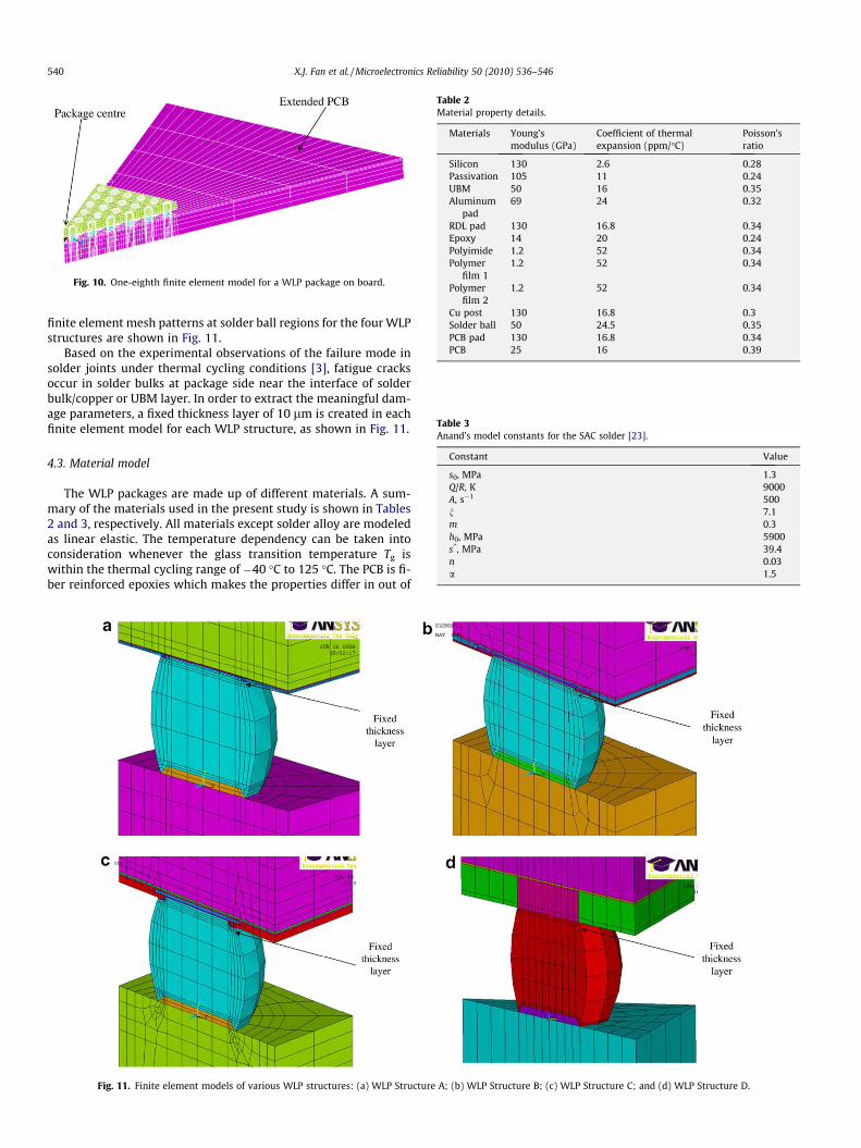
Fig. 10. One-eighth finite element model for a WLP package on board.
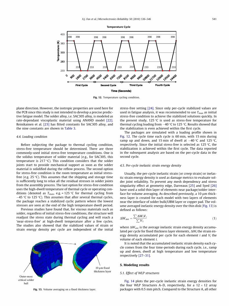
Table 2Material property details.
Materials Young’smodulus (GPa)
Coefficient of thermalexpansion (ppm/�C)
Poisson’sratio
Silicon 130 2.6 0.28Passivation 105 11 0.24UBM 50 16 0.35Aluminum
pad69 24 0.32
RDL pad 130 16.8 0.34Epoxy 14 20 0.24Polyimide 1.2 52 0.34Polymer
film 11.2 52 0.34
Polymerfilm 2
1.2 52 0.34
Cu post 130 16.8 0.3Solder ball 50 24.5 0.35PCB pad 130 16.8 0.34PCB 25 16 0.39
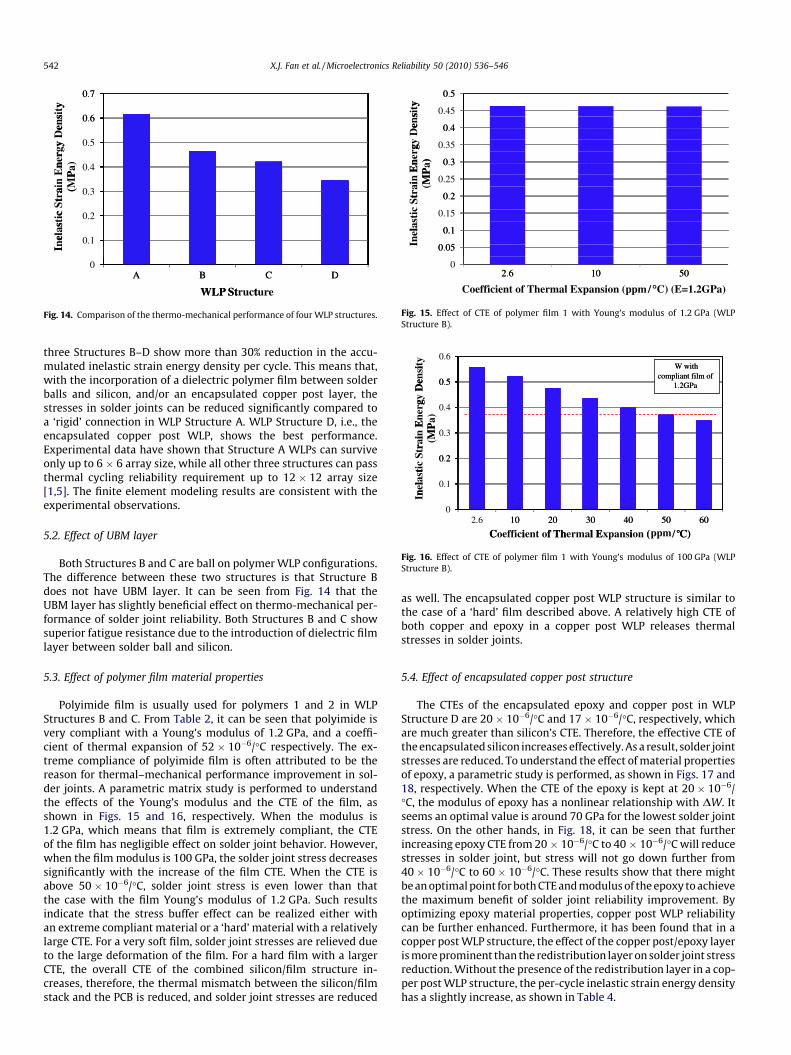
Table 3Anand’s model constants for the SAC solder [23].
Constant Value
s0, MPa 1.3Q/R, K 9000A, s�1 500n 7.1m 0.3h0, MPa 5900s^, MPa 39.4n 0.03a 1.5
540 X.J. Fan et al. / Microelectronics Reliability 50 (2010) 536–546
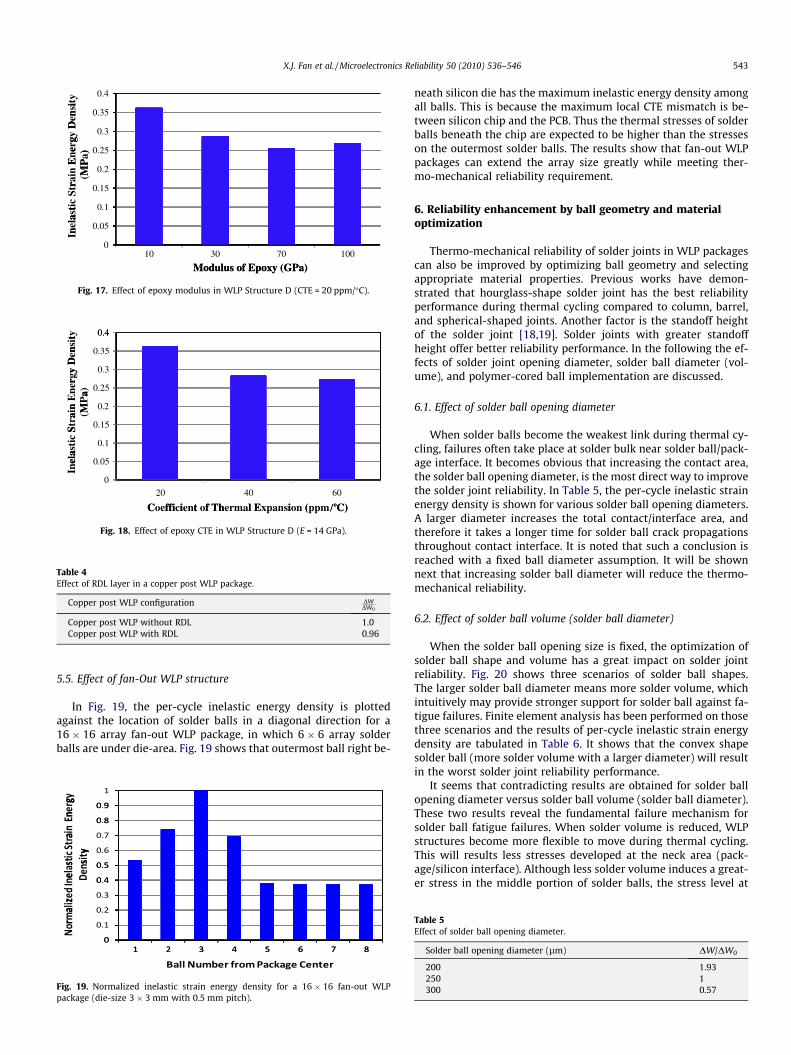
finite element mesh patterns at solder ball regions for the four WLPstructures are shown in Fig. 11.
Based on the experimental observations of the failure mode insolder joints under thermal cycling conditions [3], fatigue cracksoccur in solder bulks at package side near the interface of solderbulk/copper or UBM layer. In order to extract the meaningful dam-age parameters, a fixed thickness layer of 10 lm is created in eachfinite element model for each WLP structure, as shown in Fig. 11.
4.3. Material model
The WLP packages are made up of different materials. A sum-mary of the materials used in the present study is shown in Tables2 and 3, respectively. All materials except solder alloy are modeledas linear elastic. The temperature dependency can be taken intoconsideration whenever the glass transition temperature Tg iswithin the thermal cycling range of �40 �C to 125 �C. The PCB is fi-ber reinforced epoxies which makes the properties differ in out of
Fig. 11. Finite element models of various WLP structures: (a) WLP Structure A; (b) WLP Structure B; (c) WLP Structure C; and (d) WLP Structure D.
K)
e (K
ure
ratu
per
emp
Te
First Cycle Second Cycle Third Cycle Fourth CycleFirst Cycle Second Cycle Third Cycle Fourth Cycle
Time (Seconds)Time (Seconds)
Fig. 12. Temperature cycling condition.
X.J. Fan et al. / Microelectronics Reliability 50 (2010) 536–546 541
plane direction. However, the isotropic properties are used here forthe PCB since this study is not intended to develop a precise predic-tive fatigue model. The solder alloy, i.e. SAC305 alloy, is modeled asrate-dependant viscoplastic material using ANAND model [22].Reinikainen et al. [23] has fitted constants for SAC305 alloy, andthe nine constants are shown in Table 3.
4.4. Loading condition
Before subjecting the package to thermal cycling condition,stress-free temperature should be determined. There are threecommonly-used initial stress-free temperature conditions. One isthe solidus temperature of solder material (e.g., for SAC305, thistemperature is 217 �C). This condition considers that the solderjoints start to provide mechanical support as soon as the soldermaterial is solidified during the reflow process. The second optionfor stress-free condition is the room temperature as initial stress-free (e.g. 25 �C). This assumes that the shipping and storage timeis sufficiently long to relax all the residual stresses in solder jointsfrom the assembly process. The last option for stress-free conditionuses the high-dwell temperature of thermal cycle or operating con-ditions (denoted as Tmax, e.g. = 125 �C for thermal cycling from�45 �C to 125 �C). This assumes that after several thermal cycles,the package reaches a stabilized cyclic pattern where the loweststresses are seen at the end of the high temperature dwell period.
Previous studies have found that, for viscous materials such assolder, regardless of initial stress-free conditions, the structure willreadjust the stress state during thermal cycling and will reach a‘near-stress-free’ at high-dwell temperature after a few cycles.The studies also showed that the stabilized values of strain orstrain energy density per cycle are independent of the initial
Fig. 13. Volume averaging on a fixed thickness layer.
stress-free setting [24]. Since only per-cycle stabilized values areused in fatigue analysis, it was recommended to use Tmax as initialstress-free condition to achieve the stabilized solutions quickly. Inthe present study, 125 �C is used as stress-free temperature forthermal cycling loading from�40 �C to 125 �C. Results showed thatthe stabilization is even achieved within the first cycle.
The packages are simulated with a loading profile shown inFig. 12. The cycle time each cycle is 60 min, with 15 min duringramp up and down, and 15 min of dwell at �40 �C and 125 �C,respectively. Since the initial stress-free is selected as 125 �C, thestabilization is achieved within the first cycle. The data reportedin the subsequent analysis are based on the per-cycle data in thesecond cycle.
4.5. Per-cycle inelastic strain energy density
Usually, the per-cycle inelastic strain (or creep strain) or inelas-tic strain energy density is used as damage metrics to evaluate sol-der joint reliability. To prevent any mesh dependency and stresssingularity effect at geometry edge, Darveaux [25] and Syed [26]have used a solid thin layer of elements near package/solder inter-face for volume averaging. As described previously, a 10 lm thick-ness layer is created for each model with two layers of elementsnear the interface of solder bulk/UBM layer or copper pad. The vol-ume averaged inelastic energy density over the thin disk (Fig. 13) isdefined as follows:
DWave ¼P
DWiViPV1
ð1Þ
where DWave is the average inelastic strain energy density accumu-lated per cycle for fixed thickness layer elements, DWi the strain en-ergy density accumulated per cycle for each element i and Vi thevolume of each element i.
It is noted that the accumulated inelastic strain density each cy-cle comes from the four time-periods during each cycle, i.e., rampup and down, dwell at high temperature and low temperaturerespectively [27–31].
5. Modeling results
5.1. Effect of WLP structures
Fig. 14 plots the per-cycle inelastic strain energy densities forthe four WLP Structures A–D, respectively, for a 12 � 12 arraypackages with 0.5 mm pitch. Compared to the Structure A, all other
0 70.7
0 6
y
0.6sity
ens
0.5y D
erg
y
0.4ner
)E
nP
a
0.3ain
(MP
tra (
0.2c St
stic
0.1elas
Ine
0
I
A B C DA B C D
WLP St tWLP Structure
Fig. 14. Comparison of the thermo-mechanical performance of four WLP structures.
0 50.5
y
0.45sity
0 4ens
0.4De
0.35gy
0 3nerg
) 0.3
En
Pa)
0.25in E
MP
0 2trai (M
0.2
St
0.15tic
0.1las
0 05
0.1
nel
0.05I
02 6 10 502.6 10 50
Coefficient of Thermal Expansion (ppm/ °°C) (E=1.2GPa)
Fig. 15. Effect of CTE of polymer film 1 with Young’s modulus of 1.2 GPa (WLPStructure B).
0.6
ity
0 5ensi
0.5
De
gy D
0.4erg
En
Pa)
0.3in E
MP
rai (M
0 2Str
0.2
tic
last
0.1
nel
In
02 6 10 20 30 40 50 60. 10 20 30 40 50 60
C ffi i f Th l E i ( °C)Coe cient of Thermal Expansion (ppm/ °C)
W withW with compliant film ofcompliant film of
1.2GPa1.2GPa
Fig. 16. Effect of CTE of polymer film 1 with Young’s modulus of 100 GPa (WLPStructure B).
542 X.J. Fan et al. / Microelectronics Reliability 50 (2010) 536–546
three Structures B–D show more than 30% reduction in the accu-mulated inelastic strain energy density per cycle. This means that,with the incorporation of a dielectric polymer film between solderballs and silicon, and/or an encapsulated copper post layer, thestresses in solder joints can be reduced significantly compared toa ‘rigid’ connection in WLP Structure A. WLP Structure D, i.e., theencapsulated copper post WLP, shows the best performance.Experimental data have shown that Structure A WLPs can surviveonly up to 6 � 6 array size, while all other three structures can passthermal cycling reliability requirement up to 12 � 12 array size[1,5]. The finite element modeling results are consistent with theexperimental observations.
5.2. Effect of UBM layer
Both Structures B and C are ball on polymer WLP configurations.The difference between these two structures is that Structure Bdoes not have UBM layer. It can be seen from Fig. 14 that theUBM layer has slightly beneficial effect on thermo-mechanical per-formance of solder joint reliability. Both Structures B and C showsuperior fatigue resistance due to the introduction of dielectric filmlayer between solder ball and silicon.
5.3. Effect of polymer film material properties
Polyimide film is usually used for polymers 1 and 2 in WLPStructures B and C. From Table 2, it can be seen that polyimide isvery compliant with a Young’s modulus of 1.2 GPa, and a coeffi-cient of thermal expansion of 52 � 10�6/�C respectively. The ex-treme compliance of polyimide film is often attributed to be thereason for thermal–mechanical performance improvement in sol-der joints. A parametric matrix study is performed to understandthe effects of the Young’s modulus and the CTE of the film, asshown in Figs. 15 and 16, respectively. When the modulus is1.2 GPa, which means that film is extremely compliant, the CTEof the film has negligible effect on solder joint behavior. However,when the film modulus is 100 GPa, the solder joint stress decreasessignificantly with the increase of the film CTE. When the CTE isabove 50 � 10�6/�C, solder joint stress is even lower than thatthe case with the film Young’s modulus of 1.2 GPa. Such resultsindicate that the stress buffer effect can be realized either withan extreme compliant material or a ‘hard’ material with a relativelylarge CTE. For a very soft film, solder joint stresses are relieved dueto the large deformation of the film. For a hard film with a largerCTE, the overall CTE of the combined silicon/film structure in-creases, therefore, the thermal mismatch between the silicon/filmstack and the PCB is reduced, and solder joint stresses are reduced
as well. The encapsulated copper post WLP structure is similar tothe case of a ‘hard’ film described above. A relatively high CTE ofboth copper and epoxy in a copper post WLP releases thermalstresses in solder joints.
5.4. Effect of encapsulated copper post structure
The CTEs of the encapsulated epoxy and copper post in WLPStructure D are 20 � 10�6/�C and 17 � 10�6/�C, respectively, whichare much greater than silicon’s CTE. Therefore, the effective CTE ofthe encapsulated silicon increases effectively. As a result, solder jointstresses are reduced. To understand the effect of material propertiesof epoxy, a parametric study is performed, as shown in Figs. 17 and18, respectively. When the CTE of the epoxy is kept at 20 � 10�6/�C, the modulus of epoxy has a nonlinear relationship with DW. Itseems an optimal value is around 70 GPa for the lowest solder jointstress. On the other hands, in Fig. 18, it can be seen that furtherincreasing epoxy CTE from 20 � 10�6/�C to 40 � 10�6/�C will reducestresses in solder joint, but stress will not go down further from40 � 10�6/�C to 60 � 10�6/�C. These results show that there mightbe an optimal point for both CTE and modulus of the epoxy to achievethe maximum benefit of solder joint reliability improvement. Byoptimizing epoxy material properties, copper post WLP reliabilitycan be further enhanced. Furthermore, it has been found that in acopper post WLP structure, the effect of the copper post/epoxy layeris more prominent than the redistribution layer on solder joint stressreduction. Without the presence of the redistribution layer in a cop-per post WLP structure, the per-cycle inelastic strain energy densityhas a slightly increase, as shown in Table 4.
0.4
0 35
ity
.nsi
0 3
Den
.
gy D
0.25erg
)E
neP
a)
0.2n E
MP
0 15rai (M
.Str
0 1tic
.
ast
0.05nela
In
010 30 70 100
Modulus of Epoxy (GPa)Modulus of Epoxy (GPa)
Fig. 17. Effect of epoxy modulus in WLP Structure D (CTE = 20 ppm/�C).
0.40.4ty
0.35nsit
0 3
Den
.yD
0 25
rgy
.ner
a)
0.2n E
MP
aai
n(M
0.15Stra
0 1
c S
.
asti
0 05ela
.
Ine
020 40 60
C ffi i t f Th l E i ( °C)Coefficient of Thermal Expansion (ppm/°C)
Fig. 18. Effect of epoxy CTE in WLP Structure D (E = 14 GPa).
Table 4Effect of RDL layer in a copper post WLP package.
Copper post WLP configuration DWDW0
Copper post WLP without RDL 1.0Copper post WLP with RDL 0.96
X.J. Fan et al. / Microelectronics Reliability 50 (2010) 536–546 543
5.5. Effect of fan-Out WLP structure
In Fig. 19, the per-cycle inelastic energy density is plottedagainst the location of solder balls in a diagonal direction for a16 � 16 array fan-out WLP package, in which 6 � 6 array solderballs are under die-area. Fig. 19 shows that outermost ball right be-
Fig. 19. Normalized inelastic strain energy density for a 16 � 16 fan-out WLPpackage (die-size 3 � 3 mm with 0.5 mm pitch).
neath silicon die has the maximum inelastic energy density amongall balls. This is because the maximum local CTE mismatch is be-tween silicon chip and the PCB. Thus the thermal stresses of solderballs beneath the chip are expected to be higher than the stresseson the outermost solder balls. The results show that fan-out WLPpackages can extend the array size greatly while meeting ther-mo-mechanical reliability requirement.
6. Reliability enhancement by ball geometry and materialoptimization
Thermo-mechanical reliability of solder joints in WLP packagescan also be improved by optimizing ball geometry and selectingappropriate material properties. Previous works have demon-strated that hourglass-shape solder joint has the best reliabilityperformance during thermal cycling compared to column, barrel,and spherical-shaped joints. Another factor is the standoff heightof the solder joint [18,19]. Solder joints with greater standoffheight offer better reliability performance. In the following the ef-fects of solder joint opening diameter, solder ball diameter (vol-ume), and polymer-cored ball implementation are discussed.
6.1. Effect of solder ball opening diameter
When solder balls become the weakest link during thermal cy-cling, failures often take place at solder bulk near solder ball/pack-age interface. It becomes obvious that increasing the contact area,the solder ball opening diameter, is the most direct way to improvethe solder joint reliability. In Table 5, the per-cycle inelastic strainenergy density is shown for various solder ball opening diameters.A larger diameter increases the total contact/interface area, andtherefore it takes a longer time for solder ball crack propagationsthroughout contact interface. It is noted that such a conclusion isreached with a fixed ball diameter assumption. It will be shownnext that increasing solder ball diameter will reduce the thermo-mechanical reliability.
6.2. Effect of solder ball volume (solder ball diameter)
When the solder ball opening size is fixed, the optimization ofsolder ball shape and volume has a great impact on solder jointreliability. Fig. 20 shows three scenarios of solder ball shapes.The larger solder ball diameter means more solder volume, whichintuitively may provide stronger support for solder ball against fa-tigue failures. Finite element analysis has been performed on thosethree scenarios and the results of per-cycle inelastic strain energydensity are tabulated in Table 6. It shows that the convex shapesolder ball (more solder volume with a larger diameter) will resultin the worst solder joint reliability performance.
It seems that contradicting results are obtained for solder ballopening diameter versus solder ball volume (solder ball diameter).These two results reveal the fundamental failure mechanism forsolder ball fatigue failures. When solder volume is reduced, WLPstructures become more flexible to move during thermal cycling.This will results less stresses developed at the neck area (pack-age/silicon interface). Although less solder volume induces a great-er stress in the middle portion of solder balls, the stress level at
Table 5Effect of solder ball opening diameter.
Solder ball opening diameter (lm) DW/DW0
200 1.93250 1300 0.57
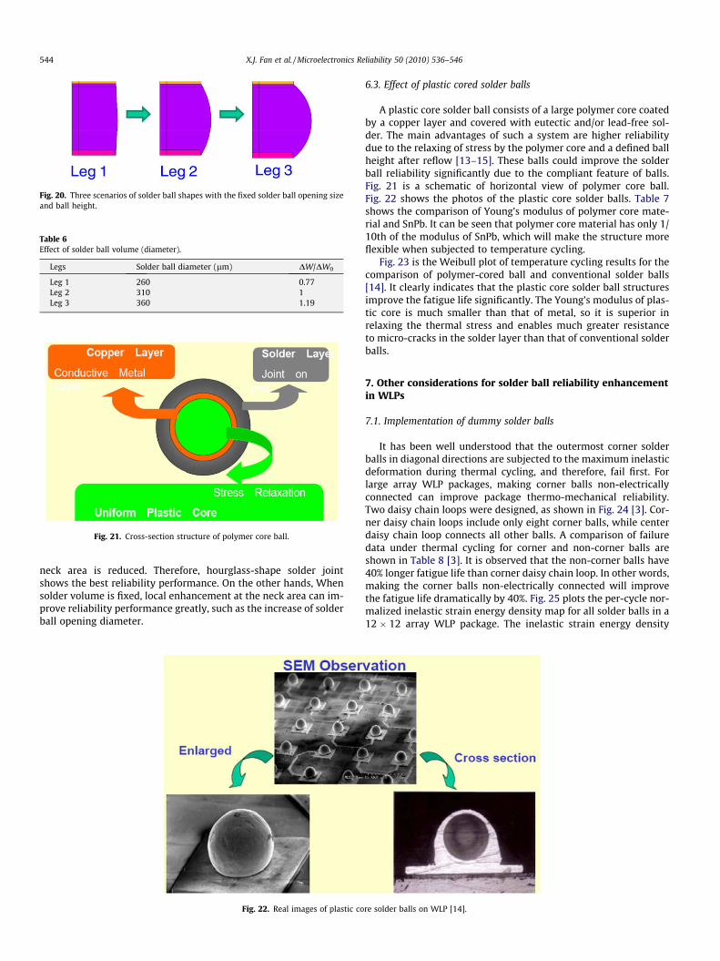
Fig. 20. Three scenarios of solder ball shapes with the fixed solder ball opening sizeand ball height.
Table 6Effect of solder ball volume (diameter).
Legs Solder ball diameter (lm) DW/DW0
Leg 1 260 0.77Leg 2 310 1Leg 3 360 1.19
Fig. 21. Cross-section structure of polymer core ball.
544 X.J. Fan et al. / Microelectronics Reliability 50 (2010) 536–546
neck area is reduced. Therefore, hourglass-shape solder jointshows the best reliability performance. On the other hands, Whensolder volume is fixed, local enhancement at the neck area can im-prove reliability performance greatly, such as the increase of solderball opening diameter.
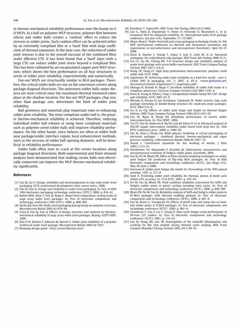
Fig. 22. Real images of plastic co
6.3. Effect of plastic cored solder balls
A plastic core solder ball consists of a large polymer core coatedby a copper layer and covered with eutectic and/or lead-free sol-der. The main advantages of such a system are higher reliabilitydue to the relaxing of stress by the polymer core and a defined ballheight after reflow [13–15]. These balls could improve the solderball reliability significantly due to the compliant feature of balls.Fig. 21 is a schematic of horizontal view of polymer core ball.Fig. 22 shows the photos of the plastic core solder balls. Table 7shows the comparison of Young’s modulus of polymer core mate-rial and SnPb. It can be seen that polymer core material has only 1/10th of the modulus of SnPb, which will make the structure moreflexible when subjected to temperature cycling.
Fig. 23 is the Weibull plot of temperature cycling results for thecomparison of polymer-cored ball and conventional solder balls[14]. It clearly indicates that the plastic core solder ball structuresimprove the fatigue life significantly. The Young’s modulus of plas-tic core is much smaller than that of metal, so it is superior inrelaxing the thermal stress and enables much greater resistanceto micro-cracks in the solder layer than that of conventional solderballs.
7. Other considerations for solder ball reliability enhancementin WLPs
7.1. Implementation of dummy solder balls
It has been well understood that the outermost corner solderballs in diagonal directions are subjected to the maximum inelasticdeformation during thermal cycling, and therefore, fail first. Forlarge array WLP packages, making corner balls non-electricallyconnected can improve package thermo-mechanical reliability.Two daisy chain loops were designed, as shown in Fig. 24 [3]. Cor-ner daisy chain loops include only eight corner balls, while centerdaisy chain loop connects all other balls. A comparison of failuredata under thermal cycling for corner and non-corner balls areshown in Table 8 [3]. It is observed that the non-corner balls have40% longer fatigue life than corner daisy chain loop. In other words,making the corner balls non-electrically connected will improvethe fatigue life dramatically by 40%. Fig. 25 plots the per-cycle nor-malized inelastic strain energy density map for all solder balls in a12 � 12 array WLP package. The inelastic strain energy density
re solder balls on WLP [14].
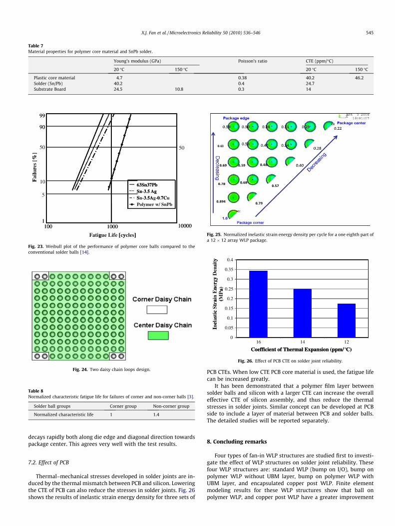
Table 7Material properties for polymer core material and SnPb solder.
Young’s modulus (GPa) Poisson’s ratio CTE (ppm/�C)
20 �C 150 �C 20 �C 150 �C
Plastic core material 4.7 0.38 40.2 46.2Solder (Sn/Pb) 40.2 0.4 24.7Substrate Board 24.5 10.8 0.3 14
9999
9090
50 50
%]
[%re
s lu
rF
ail
F 1063Sn37Pb63Sn37PbSn 3 5 Ag
5Sn-3.5 AgS 3 5A 0 7CSn-3.5Ag-0.7CuPolymer w/ SnPb
111000 10000100 1000 10000100
Fatigue Life [cycles]g [ y ]
Fig. 23. Weibull plot of the performance of polymer core balls compared to theconventional solder balls [14].
Fig. 24. Two daisy chain loops design.
Table 8Normalized characteristic fatigue life for failures of corner and non-corner balls [3].
Solder ball groups Corner group Non-corner group
Normalized characteristic life 1 1.4
Fig. 25. Normalized inelastic strain energy density per cycle for a one eighth part ofa 12 � 12 array WLP package.
0.4y
0.35
sity
0 3
ens
.y D
0 25
rgy
.ner
a)
0 2
En
Pa
.ain
(M
0.15
tra (
c St
0.1stic
elas
0.05Ine
0
I
16 14 12
Coefficient of Thermal Expansion (ppm/ °C)Coefficient of Thermal Expansion (ppm/ C)
Fig. 26. Effect of PCB CTE on solder joint reliability.
X.J. Fan et al. / Microelectronics Reliability 50 (2010) 536–546 545
decays rapidly both along die edge and diagonal direction towardspackage center. This agrees very well with the test results.
7.2. Effect of PCB
Thermal–mechanical stresses developed in solder joints are in-duced by the thermal mismatch between PCB and silicon. Loweringthe CTE of PCB can also reduce the stresses in solder joints. Fig. 26shows the results of inelastic strain energy density for three sets of
PCB CTEs. When low CTE PCB core material is used, the fatigue lifecan be increased greatly.
It has been demonstrated that a polymer film layer betweensolder balls and silicon with a larger CTE can increase the overalleffective CTE of silicon assembly, and thus reduce the thermalstresses in solder joints. Similar concept can be developed at PCBside to include a layer of material between PCB and solder balls.The detailed studies will be reported separately.
8. Concluding remarks
Four types of fan-in WLP structures are studied first to investi-gate the effect of WLP structures on solder joint reliability. Thesefour WLP structures are: standard WLP (bump on I/O), bump onpolymer WLP without UBM layer, bump on polymer WLP withUBM layer, and encapsulated copper post WLP. Finite elementmodeling results for these WLP structures show that ball onpolymer WLP, and copper post WLP have a greater improvement
546 X.J. Fan et al. / Microelectronics Reliability 50 (2010) 536–546
in thermo-mechanical reliability performance over the bump on I/O WLPs. In a ball on polymer WLP structure, polymer film betweensilicon and solder balls creates a ‘cushion’ effect to reduce thestresses in solder joints. Such cushion effect can be achieved eitherby an extremely compliant film or a ‘hard’ film with large coeffi-cient of thermal expansion. In the later case, the reduction of solderjoint stresses is due to the overall increase of the combined film/wafer effective CTE. It has been found that a ‘hard’ layer with alarge CTE can reduce solder joint stress beyond a compliant film.This has been validated by an encapsulated copper post WLP struc-ture, which shows the best performance on all four structures interms of solder joint reliability, experimentally and numerically.
Fan-out WLPs are structurally similar to BGA packages. There-fore, the critical solder balls are not on the outermost corners alongpackage diagonal directions. The outermost solder balls under die-area are most critical since the maximum thermal mismatch takesplace at die-shadow location. For fan-out WLP packages, chip size,other than package size, determines the limit of solder jointreliability.
Ball geometry and materials play important roles in enhancingsolder joint reliability. The more compliant solder ball is, the great-er thermo-mechanical reliability is achieved. Therefore, reducingindividual solder ball volume or using more compliant materialssuch as polymer-cored solder balls will improve reliability perfor-mance. On the other hands, since failures are often at solder bulknear package/solder interface region, local enhancement methods,such as the increase of solder ball opening diameter, will be bene-ficial in reliability performance.
Solder balls often start to crack at the corner locations alongpackage diagonal directions. Both experimental and finite elementanalysis have demonstrated that making corner balls non-electri-cally connected can improve the WLP thermo-mechanical reliabil-ity significantly.
References
[1] Fan XJ, Liu Y. Design, reliability and electromigration in chip scale wafer levelpackaging. ECTC professional development short course notes; 2009.
[2] Fan XJ, Han Q. Design and reliability in wafer level packaging. In: Proc of IEEE10th electronics packaging technology conference (EPTC); 2008. p. 834–41.
[3] Rahim MSK, Zhou T, Fan XJ, Rupp G. Board level temperature cycling study oflarge array wafer level packages. In: Proc of electronic components andtechnology conference (59th ECTC); 2009. p. 898–902
[4] Reche JHJ, Kim DH. Wafer level packaging having bump-on-polymer structure.Microelectron Reliab 2003;43:879–94.
[5] Varia B, Fan XJ, Han Q. Effects of design, structure and material on thermal–mechanical reliability of large array wafer level packages. Beijing: ICEPT-HDP;2009.
[6] Kim D-H, Elenius P, Johnson M, Barrett S. Solder joint reliability of a polymerreinforced wafer level package. Microelectron Reliab 2002;42:1837.
[7] Bumping design guide. <http://www.flipchip.com/>.
[8] Kawahara T. SuperCSPs. IEEE Trans Adv Packag 2002;23(2):2002.[9] Gao G, Haba B, Organesian V, Honer H, Ovrutsky D, Rosenstein C, et al.
Compliant WLP for enhanced reliability. In: International wafer level packageconference, San Jose (CA); September 17–19 2007.
[10] Meyer-Berg G. Wafer-level ball grid array packaging technology trends. In: 9thIEEE international conference on thermal and mechanical simulation andexperiments in microelectronics and microsystems (EuroSimE); April 20–232008.
[11] Keser B, Amrine C, Duong T, Hayes S, Leal G, Lytle M, et al. Advancedpackaging: the redistributed chip package. IEEE Trans Adv Packag 2008;31(1).
[12] Lee CC, Liu HC, Chiang KN. 3-D structure design and reliability analysis ofwafer level package with stress buffer mechanism. IEEE Trans Compon PackagTechnol 2007;30(1):110–8.
[13] Wang YP, Hung LY. High drop performance interconnection: polymer coredsolder ball. ECTC 2008.
[14] Eagelmaier W. Achieving solder joint reliability in a lead-free world – part 2.Global SMT & packaging, vol. 7; 2007. p. 45–6. <www.globalsmt.net/documents/Columns-Engelmaier/7.7_engelmaier.pdf>.
[15] Okinaga N, Kuroda H, Nagai Y. Excellent reliability of solder ball made of acompliant plasticcore. Electron Compon Technol Conf 2001:1345–9.
[16] Keser B, Yeung B, White J, Fang T. Encapsulated double-bump WL-CSP: designand reliability. ECTC 2001:35–9.
[17] Mitsuka K, Kurata H, Jun Furukawa, Takahashi M. Wafer process chip scalepackage consisting of double-bump structure for small-pin-count packages.ECTC 2005:572–6.
[18] Liu X, Lu GQ. Effects of solder joint shape and height on thermal fatiguelifetime. IEEE Trans Compon Packag Technol 2003;26(2):455–65.
[19] Lim SS, Rajoo R, Wong EH. Reliability performance of stretch solderinterconnections. In: Proc IEMT; 2006.
[20] Tee TY, Tan LB, Anderson R, Ng HS, Low JH, Khoo CP, et al. Advanced analysis ofWLCSP copper interconnect reliability under board level drop test. In: 10thEPTC conference proc.; 2008. p. 1086–95.
[21] Fan XJ, Zhou J, Zhang GQ. Multi-physics modeling in virtual prototyping ofelectronic packages – combined thermal, thermo-mechanical and vaporpressure modeling. J Microelectron Reliab 2004;44:1967–76.
[22] Anand L. Constitutive equations for hot working of metals. J Plast1985;1:213–31.
[23] Reinikainen TO, Marjamäki P, Kivilahti JK. Deformation characteristics andmicrostructural evolution of SnAgCu solder joints. EuroSimE; 2005.
[24] Fan XJ, Pei M, Bhatti PK. Effect of finite element modeling techniques on solderjoint fatigue life prediction of flip-chip BGA packages. In: Proc of IEEEelectronic components and technology conference (ECTC), San Diego (CA);May 30–June 2 2006.
[25] Darveaux R. Solder joint fatigue life model. In: Proceedings of the TMS annualmeeting; 1997. p. 213–8.
[26] Syed A. Predicting solder joint reliability for thermal, power, & bend cyclewithin 25% accuracy. In: 51st ECTC; 2001. p. 255–63.
[27] Pei M, Fan XJ, Bhatti PK. Field condition reliability assessment for SnPb andSnAgCu solder joints in power cycling including mini cycles. In: Proc ofelectronic components and technology conference (ECTC); 2006. p. 899–905
[28] Bhatti PK, Pei M, Fan XJ. Reliability analysis of SnPb and SnAgCu solder joints inFC-BGA packages with thermal enabling preload. In: Proc of electroniccomponents and technology conference (ECTC); 2006. p. 601–6.
[29] Fan XJ, Rasier G, Vasudevan VS. Effects of dwell time and ramp rate on lead-free solder joints in FCBGA packages. In: Proc of electronic components andtechnology conference (ECTC); 2005. p. 901–6.
[30] Vasudevan V, Fan X, Liu T, Young D. Slow cycle fatigue creep performance ofPb-Free (LF) solders. In: Proc of electronic components and technologyconference (ECTC); 2007. p. 116–23.
[31] Fan XJ, Wang HB, Lim TB. Investigation of the underfill delamination andcracking for flip chip module during thermal cyclic loading. IEEE TransCompon Manufact Packag Technol 2001;24(1):84–91.