Design and Implementation of Cost-effective Simple FIR ...
17
Available online at www.worldscientificnews.com ( Received 04 March 2019; Accepted 20 March 2019; Date of Publication 21 March 2019 ) WSN 125 (2019) 1-17 EISSN 2392-2192 Design and Implementation of Cost-effective Simple FIR Filter for EEG Signal on FPGA Atik Mahabub Department of Electronics and Communication Engineering, Khulna University of Engineering & Technology,Khulna, Bangladesh E-mail address: [email protected] ABSTRACT Filter is immensely used to distinguish distinctive human signal progressively. In this article, a digital finite impulse response (FIR) filter is presented for the quick detection of electroencephalogram (EEG) signal to smooth and compress the signal. This paper means to structure an advanced FIR filter based on Field Programmable Gate Array (FPGA) to get faster biomedical signals specially EEG signals. For this respect, a simple and cost-effective FIR filter is introduced to make EEG signal noise free, less costly, less power consuming and simple. It requires less space for chip implementation than other digital filter and avoid the mixture of other biomedical signal. For hardware execution, FPGA board is utilized which is a mix of various logic gates and registers which offers cheap and dependable administrations. Keywords: FPGA, Cost-effective, FIR, EEG, RTL, Floor Plan 1. INTRODUCTION FIR filters are utilized in many digital applications like image processing, wireless communication, biomedical etc. [1]. Customary filtering executions have been processor situated, where the structure procedure mostly comprises of building up the important abnormal state code with some idea given to the hidden design to streamline the code quality [2].
Transcript of Design and Implementation of Cost-effective Simple FIR ...
Available online at www.worldscientificnews.com
( Received 04 March 2019; Accepted 20 March 2019; Date of Publication 21 March 2019 )
WSN 125 (2019) 1-17 EISSN 2392-2192
Design and Implementation of Cost-effective Simple FIR Filter for EEG Signal on FPGA
Atik Mahabub
Department of Electronics and Communication Engineering, Khulna University of Engineering & Technology,Khulna, Bangladesh
E-mail address: [email protected]
ABSTRACT
Filter is immensely used to distinguish distinctive human signal progressively. In this article,
a digital finite impulse response (FIR) filter is presented for the quick detection of
electroencephalogram (EEG) signal to smooth and compress the signal. This paper means to
structure an advanced FIR filter based on Field Programmable Gate Array (FPGA) to get faster
biomedical signals specially EEG signals. For this respect, a simple and cost-effective FIR filter is
introduced to make EEG signal noise free, less costly, less power consuming and simple. It requires
less space for chip implementation than other digital filter and avoid the mixture of other biomedical
signal. For hardware execution, FPGA board is utilized which is a mix of various logic gates and
registers which offers cheap and dependable administrations.
Keywords: FPGA, Cost-effective, FIR, EEG, RTL, Floor Plan
1. INTRODUCTION
FIR filters are utilized in many digital applications like image processing, wireless
communication, biomedical etc. [1]. Customary filtering executions have been processor
situated, where the structure procedure mostly comprises of building up the important abnormal
state code with some idea given to the hidden design to streamline the code quality [2].
World Scientific News 125 (2019) 1-17
-2-
However, the iterative nature of filtering algorithms can be abused to uncover concealed
concurrencies both inside emphasis and among various iterations [3]. This has given originators
adequate driving force to search for stage arranged arrangements, where the hidden equipment
can be used to build up a SoC-based arrangement that best matches the algorithmic multifaceted
nature by building up the correct dimension of parallelism. In like manner, endeavors have been
made to create custom and reconfigurable models for acknowledging FIR filters on ASIC and
FPGA stages [4]. However, with ASICs the non-recurring engineering (NRE) costs involved
are huge. This ordinarily has cornered ASICs to high volume creations. FPGAs maintain a
strategic distance from high NRE costs by giving the client the adaptability of arranging [5]. Be
that as it may, with ASICs the non-repeating designing (NRE) costs included are enormous [6].
Some other advantages include large-scale integration [3, 7] lower energy requirements using
the same process technology [8, 3] availability of several on-board IP cores [9] etc. FPGAs vary
definitely from ASICs. Not at all like ASICs, the fundamental texture can be utilized to execute
a wide scope of functionalities, essentially lessening the long structure time related with ASICs
[5]. The structure cycle in FPGAs is a lot more straightforward as the product handles the
tedious steering, situation and floor arranging stages. This confines the viability of the
innovation free streamlining systems that are commonly appropriate for ASICs [1].
Additionally the decision of the objective family will prominently affect the end execution of
the actualized structure [10]. Thus, complete information about the target device is necessary.
An electroencephalogram is a sort of signs which is low in quality. The power ranges
from 150 to 290 microvolts. These signs began from the human mind is the graphical sketch of
the cerebrum movement. In the recurrence space, there is a scaling from 0.5 Hz to 100 Hz [11,
12]. Furthermore, this particular scaling absolutely has a place with the recurrence idea of
electroencephalogram signals.
Presently truly, this paper is endeavoring to actualize it to structure a test show for
distinguishing electroencephalogram signal. Yet, from the past it tends to be guaranteed that
the recognition of the EEG signal isn't a simple undertaking. Besides, look into related with
planning an equipment structure for identifying and breaking down electroencephalogram
signal demonstrating that it is a tranquil complex work. Consequently it is a non-stationary sign
however its capacity unearthly investigation is very important.
In the paper of novel complete filter [13], a new filter has been invented for the detection
of EEG signal by using FPGA. It is a combination of integration and differentiator filters. It has
been used for mainly to remove noises and to detect EEG signal. But it has some problems like
more quantization level, more area is required and uses threshold system for removing noise
for hardware implementation. These make this filter less effective and costlier. But using FIR
filter these problems can be solved and here in this paper, these things will be discussed briefly.
The gaining popularity as use of oversampled an effective digital method for building is
rapidly high resolution analog-to-digital (A/D) and digital-to-analog (D/A) converters [14].
While oversampled converters usually interface to digital signals at the nyquist rate, it is useful
to consider signal processing directly at the oversampled rate in an attempt to save valuable
silicon area. One technique for processing digital signals is to make use of finite-impulse-
response (FIR) filters [15-16]. In general, FIR filters use normal multiplier to multiply
coefficients. The normal array multiplier occupies much area and consumes considerable
amount of power. Hence, to improve the performance of the multiplier, many researchers are
working to develop efficient multiplier which provides area efficiency and power efficiency
[17-19]. For low power designs, variable input word-length and number of channel taps, diverse
World Scientific News 125 (2019) 1-17
-3-
coefficient word-lengths, and element minimized flag representation procedures are utilized. In
those works, vast overhead is brought about to bolster reconfigurable plans, for example, self-
assertive nonzero digit task or programmable move [17-22].
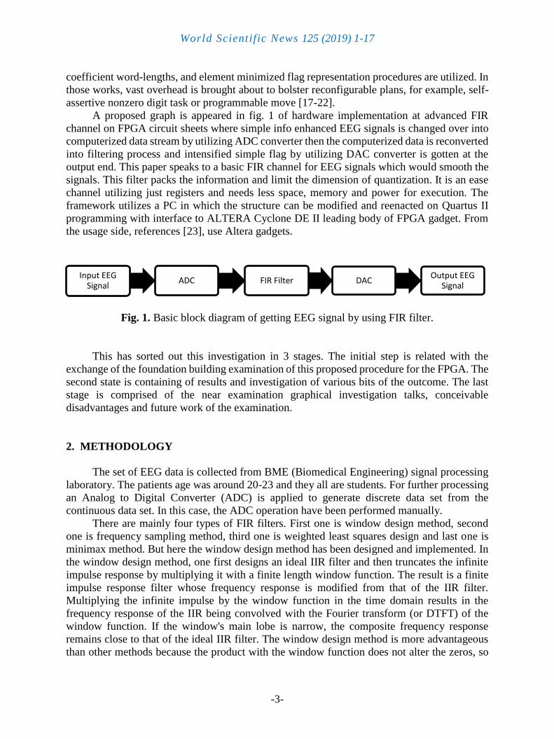
A proposed graph is appeared in fig. 1 of hardware implementation at advanced FIR
channel on FPGA circuit sheets where simple info enhanced EEG signals is changed over into
computerized data stream by utilizing ADC converter then the computerized data is reconverted
into filtering process and intensified simple flag by utilizing DAC converter is gotten at the
output end. This paper speaks to a basic FIR channel for EEG signals which would smooth the
signals. This filter packs the information and limit the dimension of quantization. It is an ease
channel utilizing just registers and needs less space, memory and power for execution. The
framework utilizes a PC in which the structure can be modified and reenacted on Quartus II
programming with interface to ALTERA Cyclone DE II leading body of FPGA gadget. From
the usage side, references [23], use Altera gadgets.
Fig. 1. Basic block diagram of getting EEG signal by using FIR filter.
This has sorted out this investigation in 3 stages. The initial step is related with the
exchange of the foundation building examination of this proposed procedure for the FPGA. The
second state is containing of results and investigation of various bits of the outcome. The last
stage is comprised of the near examination graphical investigation talks, conceivable
disadvantages and future work of the examination.
2. METHODOLOGY
The set of EEG data is collected from BME (Biomedical Engineering) signal processing
laboratory. The patients age was around 20-23 and they all are students. For further processing
an Analog to Digital Converter (ADC) is applied to generate discrete data set from the
continuous data set. In this case, the ADC operation have been performed manually.
There are mainly four types of FIR filters. First one is window design method, second
one is frequency sampling method, third one is weighted least squares design and last one is
minimax method. But here the window design method has been designed and implemented. In
the window design method, one first designs an ideal IIR filter and then truncates the infinite
impulse response by multiplying it with a finite length window function. The result is a finite
impulse response filter whose frequency response is modified from that of the IIR filter.
Multiplying the infinite impulse by the window function in the time domain results in the
frequency response of the IIR being convolved with the Fourier transform (or DTFT) of the
window function. If the window's main lobe is narrow, the composite frequency response
remains close to that of the ideal IIR filter. The window design method is more advantageous
than other methods because the product with the window function does not alter the zeros, so
Input EEG Signal
ADC FIR Filter DACOutput EEG
Signal
World Scientific News 125 (2019) 1-17
-4-
almost half of the coefficients of the final impulse response are zero. An appropriate
implementation of the FIR calculations can exploit that property to double the filter's efficiency.
The filtering process is used after the ADC operation. Here FIR filter will be used for the
filtering process. Consider N-point digital FIR filter, is characterized by the following
difference equation:
𝑦(𝑛) = ∑ ℎ𝑛𝑁𝑛=0 𝑥[𝑛 − 𝑁] (1)
where 𝑥(𝑛) represents the latest input sample, 𝑦(𝑛) the output sample, N defines the order of
the filter, 𝑦(𝑛) is the value of the impulse response at the n-th instant for 0≤ n ≤ N of an N-th-
order FIR filter. The impulse response can be defined as:
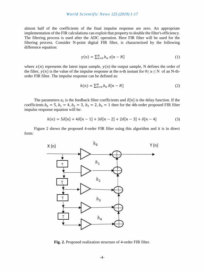
ℎ(𝑛) = ∑ 𝑏𝑛𝑁𝑛=0 𝛿[𝑛 − 𝑁] (2)
The parameters 𝑎𝑖 is the feedback filter coefficients and 𝛿[𝑛] is the delay function. If the
coefficients 𝑏0 = 5, 𝑏1 = 4, 𝑏2 = 3, 𝑏3 = 2, 𝑏4 = 1 then for the 4th-order proposed FIR filter
impulse response equation will be:
ℎ(𝑛) = 5𝛿[𝑛] + 4𝛿[𝑛 − 1] + 3𝛿[𝑛 − 2] + 2𝛿[𝑛 − 3] + 𝛿[𝑛 − 4] (3)
Figure 2 shows the proposed 4-order FIR filter using this algorithm and it is in direct
form:
Fig. 2. Proposed realization structure of 4-order FIR filter.
World Scientific News 125 (2019) 1-17
-5-
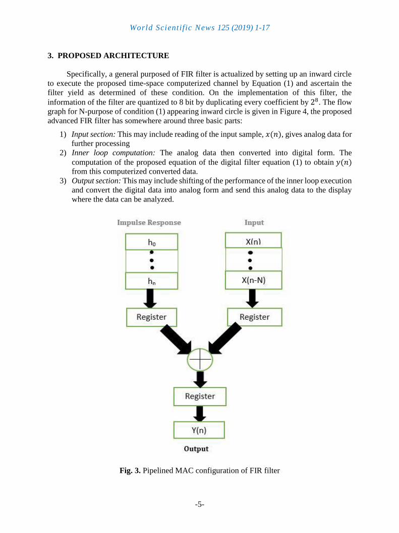
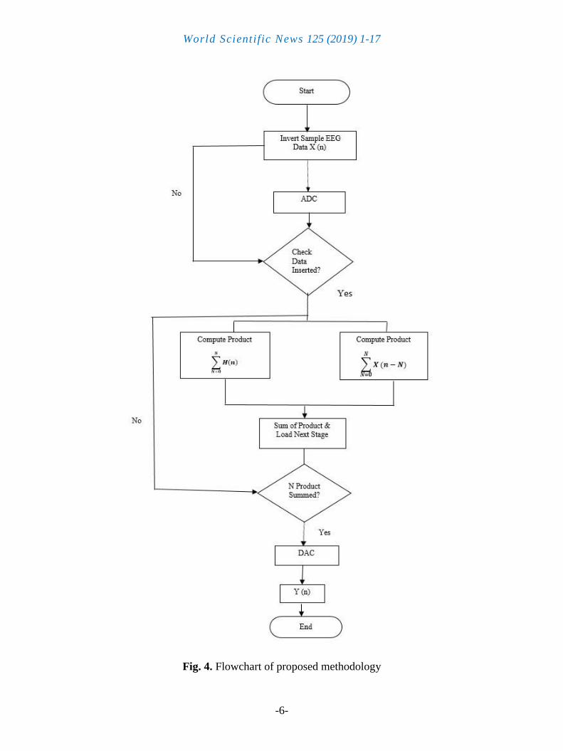
3. PROPOSED ARCHITECTURE
Specifically, a general purposed of FIR filter is actualized by setting up an inward circle
to execute the proposed time-space computerized channel by Equation (1) and ascertain the
filter yield as determined of these condition. On the implementation of this filter, the
information of the filter are quantized to 8 bit by duplicating every coefficient by 28. The flow
graph for N-purpose of condition (1) appearing inward circle is given in Figure 4, the proposed
advanced FIR filter has somewhere around three basic parts:
1) Input section: This may include reading of the input sample, 𝑥(𝑛), gives analog data for
further processing
2) Inner loop computation: The analog data then converted into digital form. The
computation of the proposed equation of the digital filter equation (1) to obtain 𝑦(𝑛)
from this computerized converted data.
3) Output section: This may include shifting of the performance of the inner loop execution
and convert the digital data into analog form and send this analog data to the display
where the data can be analyzed.
Fig. 3. Pipelined MAC configuration of FIR filter
World Scientific News 125 (2019) 1-17
-6-
Fig. 4. Flowchart of proposed methodology
World Scientific News 125 (2019) 1-17
-7-
Fig. 5. RTL diagram of the proposed model

World Scientific News 125 (2019) 1-17
-8-
Here step-1 is the system dependent, we will work on the inner loop execution and output
section in here. The proposed FIR filter inner loop will be executed with the following
instruction in ALTRA Cyclone II board with processors EP2C35F672C.
In this case, the coefficients and data memories are utilized as shown in Fig. 4. The
registers AR1, AR2, AR3, AR4, AR5 are used for indirect execution of the inner loop
computation and initially points to last input stream 𝑥(𝑛 − 1) in the data memory. The
following instructions are computing in the inner loop such as
a. Adds the previous products to the accumulator e.g. initially, the products are zero.
b. Multiply the window function ℎ0 by the data memory 𝑥(𝑛) and store it into AR1
c. Multiply the window function ℎ1 by the data memory 𝑥(𝑛 − 1) and add it with the AR1
and store it into AR2. This process is continued for AR4.
d. Multiply the window function ℎ4 by the data memory 𝑥(𝑛 − 4) and add it with the AR4
and store it into AR5 which is the output y(n).
The stream and coefficient storages for the direct structure is shown in Fig. 3 & 4.
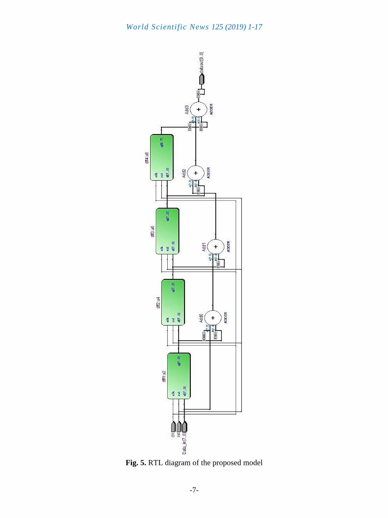
4. DESCRIPTION OF RTL BLOCKS
Data_in
It is a register type structure which briefly stores the info EEG signal esteem and it serves
this incentive to the dff1: u2 in agreement to the control ROM bit successions. It is an 8-bit
register.
Data_out
It is likewise a register type module which incidentally store the qualities after the
procedure of Add3 and gives it to the peripherals of the framework. It is a 10-bit register. It is
the ideal yield.
Clk
Clk is utilized to send pulses to the flip-flops. It is a solitary piece register. It tallies cycles
and information can be goes through registers.
Rst
It is a solitary piece register which used to set the estimation of information to an
underlying stage and invigorate the ROM memory. Reset is utilized toward the beginning of
each new procedure.
dff1:u2 – dff4:u8
It is a register which stores the co-efficients from b0, b2, …., b4. It passes the data to the
Add and the next dff register for quick calculations. The first dff1:u2 takes the input data and
multiply with window function h0 and send it to Add0. The dff2:u4 takes the output data dff1:u2
and multiply with window function h1 and send it to Add1. This process is continued for other
dff3:u6 and dff4:u8 similarly.
World Scientific News 125 (2019) 1-17
-9-
Add0 - Add3
It is a register type module used to add data Add0 is used to add input data with dff1:u2
and send it to Add1. Add1 takes it and add it with dff2:u4 and send it to Add2. Add2 takes it
and add it with dff3:u6 and send it to Add3. Add3 takes it and add it with dff4:u8 and send it to
Data_out which is the output.
Figure 5 shows the RTL diagram for the proposed FIR filter.
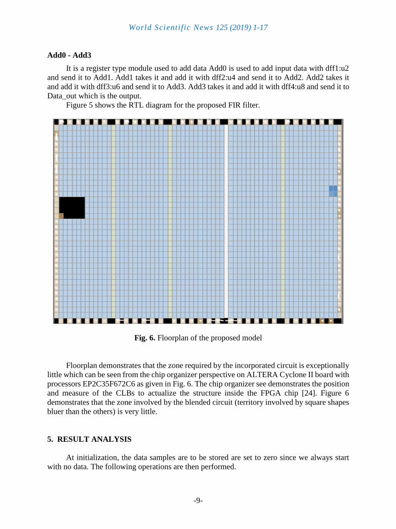
Fig. 6. Floorplan of the proposed model
Floorplan demonstrates that the zone required by the incorporated circuit is exceptionally
little which can be seen from the chip organizer perspective on ALTERA Cyclone II board with
processors EP2C35F672C6 as given in Fig. 6. The chip organizer see demonstrates the position
and measure of the CLBs to actualize the structure inside the FPGA chip [24]. Figure 6
demonstrates that the zone involved by the blended circuit (territory involved by square shapes
bluer than the others) is very little.
5. RESULT ANALYSIS
At initialization, the data samples are to be stored are set to zero since we always start
with no data. The following operations are then performed.
World Scientific News 125 (2019) 1-17
-10-
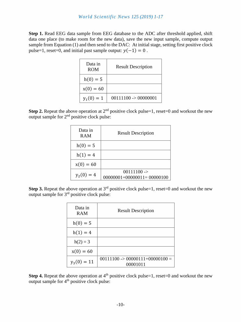
Step 1. Read EEG data sample from EEG database to the ADC after threshold applied, shift
data one place (to make room for the new data), save the new input sample, compute output
sample from Equation (1) and then send to the DAC: At initial stage, setting first positive clock
pulse=1, reset=0, and initial past sample output: 𝑦(−1) = 0 .
Data in
ROM Result Description
h(0) = 5
x(0) = 60
y1(0) = 1 00111100 -> 00000001
Step 2. Repeat the above operation at 2nd positive clock pulse=1, reset=0 and workout the new
output sample for 2nd positive clock pulse:
Data in
RAM Result Description
h(0) = 5
h(1) = 4
x(0) = 60
y2(0) = 4 00111100 ->
00000001+00000011= 00000100
Step 3. Repeat the above operation at 3rd positive clock pulse=1, reset=0 and workout the new
output sample for 3rd positive clock pulse:
Data in
RAM Result Description
h(0) = 5
h(1) = 4
h(2) = 3
x(0) = 60
y3(0) = 11 00111100 -> 00000111+00000100 =
00001011
Step 4. Repeat the above operation at 4th positive clock pulse=1, reset=0 and workout the new
output sample for 4th positive clock pulse:
World Scientific News 125 (2019) 1-17
-11-
Data in RAM Result Description
h(0) = 5
h(1) = 4
h(2) = 3
h(3) = 4
x(0) = 60
y4(0) = 26 00111100 -> 00001111+00001011 =
00011010
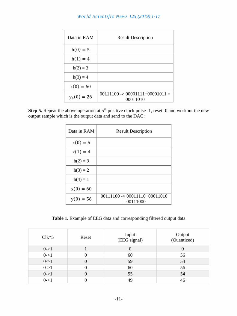
Step 5. Repeat the above operation at 5th positive clock pulse=1, reset=0 and workout the new
output sample which is the output data and send to the DAC:
Data in RAM Result Description
x(0) = 5
x(1) = 4
h(2) = 3
h(3) = 2
h(4) = 1
x(0) = 60
y(0) = 56 00111100 -> 00011110+00011010
= 00111000
Table 1. Example of EEG data and corresponding filtered output data
Clk*5 Reset Input
(EEG signal)
Output
(Quantized)
0->1 1 0 0
0->1 0 60 56
0->1 0 59 54
0->1 0 60 56
0->1 0 55 54
0->1 0 49 46
World Scientific News 125 (2019) 1-17
-12-
These similar things happen for other input data also. Here only single data is detailed
described.
Table 1 demonstrates the examinations among info and yield information of the FIR filter.
The info information is the EEG signs, integrator yield is the yield of the integrator filter, hold
is utilized for to see a particular information, yield (quantized) is the first yield information of
the proposed filter which is the EEG signs.
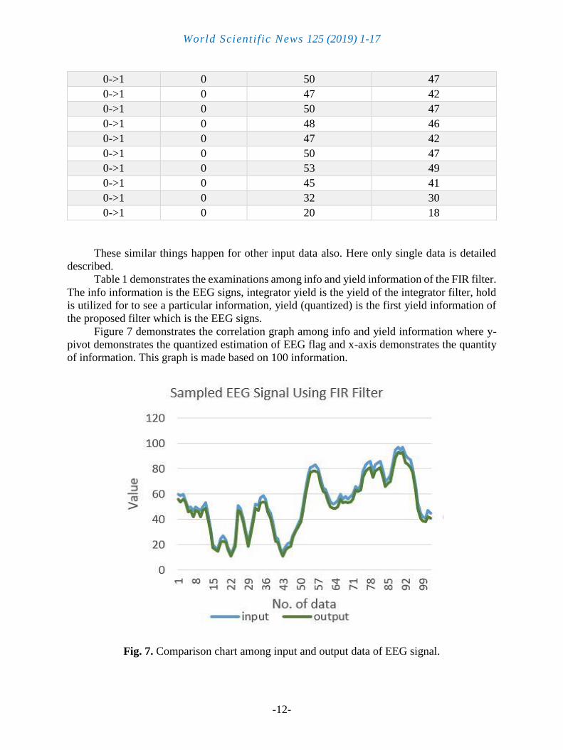
Figure 7 demonstrates the correlation graph among info and yield information where y-
pivot demonstrates the quantized estimation of EEG flag and x-axis demonstrates the quantity
of information. This graph is made based on 100 information.
Fig. 7. Comparison chart among input and output data of EEG signal.
0->1 0 50 47
0->1 0 47 42
0->1 0 50 47
0->1 0 48 46
0->1 0 47 42
0->1 0 50 47
0->1 0 53 49
0->1 0 45 41
0->1 0 32 30
0->1 0 20 18
World Scientific News 125 (2019) 1-17
-13-
(a)
(b)
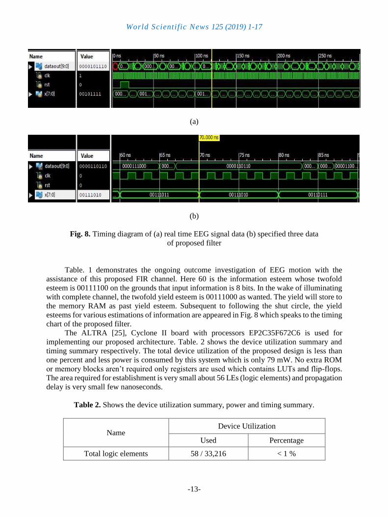
Fig. 8. Timing diagram of (a) real time EEG signal data (b) specified three data
of proposed filter
Table. 1 demonstrates the ongoing outcome investigation of EEG motion with the
assistance of this proposed FIR channel. Here 60 is the information esteem whose twofold
esteem is 00111100 on the grounds that input information is 8 bits. In the wake of illuminating
with complete channel, the twofold yield esteem is 00111000 as wanted. The yield will store to
the memory RAM as past yield esteem. Subsequent to following the shut circle, the yield
esteems for various estimations of information are appeared in Fig. 8 which speaks to the timing
chart of the proposed filter.
The ALTRA [25], Cyclone II board with processors EP2C35F672C6 is used for
implementing our proposed architecture. Table. 2 shows the device utilization summary and
timing summary respectively. The total device utilization of the proposed design is less than
one percent and less power is consumed by this system which is only 79 mW. No extra ROM
or memory blocks aren’t required only registers are used which contains LUTs and flip-flops.
The area required for establishment is very small about 56 LEs (logic elements) and propagation
delay is very small few nanoseconds.
Table 2. Shows the device utilization summary, power and timing summary.
Name Device Utilization
Used Percentage
Total logic elements 58 / 33,216 < 1 %
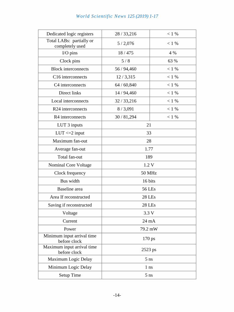
World Scientific News 125 (2019) 1-17
-14-
Dedicated logic registers 28 / 33,216 < 1 %
Total LABs: partially or
completely used 5 / 2,076 < 1 %
I/O pins 18 / 475 4 %
Clock pins 5 / 8 63 %
Block interconnects 56 / 94,460 < 1 %
C16 interconnects 12 / 3,315 < 1 %
C4 interconnects 64 / 60,840 < 1 %
Direct links 14 / 94,460 < 1 %
Local interconnects 32 / 33,216 < 1 %
R24 interconnects 8 / 3,091 < 1 %
R4 interconnects 30 / 81,294 < 1 %
LUT 3 inputs 21
LUT <=2 input 33
Maximum fan-out 28
Average fan-out 1.77
Total fan-out 189
Nominal Core Voltage 1.2 V
Clock frequency 50 MHz
Bus width 16 bits
Baseline area 56 LEs
Area If reconstructed 28 LEs
Saving if reconstructed 28 LEs
Voltage 3.3 V
Current 24 mA
Power 79.2 mW
Minimum input arrival time
before clock 170 ps
Maximum input arrival time
before clock 2523 ps
Maximum Logic Delay 5 ns
Minimum Logic Delay 1 ns
Setup Time 5 ns
World Scientific News 125 (2019) 1-17
-15-
6. CONCLUSIONS
This paper represents an implementation of simple forth order FIR filter for EEG signal.
This FIR filter is more effective and simpler than the IIR filter usage less memory and response
faster. are more helpful than some other computerized framework and using Verilog HDL exact
synthesized result and RTL schematic has been built up. The proposed technique is minimal
effort, elite, self-reconfigurable, flexible and simple to actualize. This proposed architecture can
be useful for real time EEG signal detection application. It is a very cost effective concept which
can be helpful to measure and detect EEG signal. This FIR filter will require less space if it is
implemented in chip and would give better output results. In future, this proposition can be
planned and actualized for other biomedical signs to make it increasingly compelling.
References
[1] Khurshid, Burhan, and Roohie Naaz Mir. An efficient FIR filter structure based on
technology-optimized multiply-adder unit targeting LUT-based FPGAs. Circuits,
Systems, and Signal Processing 36, no. 2 (2017) 600-639
[2] J.E. Carletta, M.D. Rayman, Practical Considerations in the Synthesis of High
Performance Digital Filters for Implementation on FPGAs. FPL 2002, LNCS 2438, pp.
886–896, Springer, (2002).
[3] C. Cheng, K.K. Parhi, Hardware efficient fast parallel FIR filter structures based on
iterated short convolution. IEEE Trans. Circ. Syst. I Reg. Pap. 51(8), 1492–1500
(2004).
[4] L. Deng, K. Sobti, Y. Zhang, C. Chakarbarti, Accurate area, time and power models for
FPGA based implementations. J. Signal Process. Syst. 63, 39–50 (2011).
[5] R. Naseer, M. Balakrishnan, A. Kumar, Direct Mapping of RTL Structures onto LUT-
Based FPGAs, IEEE Transactions on Computer-Aided Design of Integrated Circuits
and Systems, Vol. 17, No. 7, (1998).
[6] P. Shi, Y.J. Yu, Design of linear phase FIR filters with high probability of achieving
minimum number of adders. IEEE Circ. Syst. Soc. 58(1), 126–136 (2011).
[7] G. Stitt, F. Vahid, S. Nematbakhsh, Energy savings and speed-ups from partitioning
critical software loops to hardware in embedded systems. ACM Trans. Embed. Comput.
Syst. 3(1), 218–232 (2004).
[8] Y.C. Tsao, K. Choi, Area efficient parallel FIR digital filter structures for symmetric
convolutions based on fast FIR algorithm. IEEE Trans. VLSI Syst. 20(2), 366–371
(2010)
[9] Y.C. Tsao, K. Choi, Area efficient VLSI implementation for parallel linear-phase FIR
digital filters of odd length based on fast FIR algorithm. IEEE Trans. Circ. Syst.-II
Express Briefs 59(6), 371–375, (2012)
[10] N. Verma, A. Shoeb, J. Bohorquez, J. Dawson, J. Guttag, and A. Chandrakasan, A
micro-power EEG acquisition SoC with integrated feature extraction processor for a

World Scientific News 125 (2019) 1-17
-16-
chronic seizure detection system. IEEE J. Solid-State Circuits, vol. 45, no. 4, pp. 804–
816, 2010.
[11] E. Niedermeyer, F. H. Lopes da Silva, Electroencephalography: Basic Principles,
Clinical Applications, and Related Fields. Lippincott Williams & Wilkins, 2005 Sixth
edition, ISBN-13: 978-0781789424
[12] John G. Webster. Medical Instrumentation Application and Design. John Wiley and
Sons INC. 2001 Third edition, ISBN: 9971-51-270-X.
[13] Atik Mahabub, Design and Implementation of a Novel Complete Filter for EEG
Application on FPGA. International Journal of Image, Graphics and Signal Processing
Vol. 10, No. 6, pp. 22-30, 2018. DOI: 10.5815/ijigsp.2018.06.03
[14] JW Fattaruso, LA Williams III Oversampled Analog-to-Digital and Digital-to Analog
Converters. The VLSI Handbook. Ed. Wai-Kai Chen Boca Raton: CRC Press LLC,
2000.
[15] S. Rengaprakash, M. Vignesh, N. Syed Anwar, M. Pragadheesh, E. Senthilkumar, M.
Sandhya, J. Manikandan, FPGA implementation of fast running FIR filters. 2017
International Conference on Wireless Communications, Signal Processing and
Networking, Year: 2017, Page s: 1282 - 1286
[16] Patrick Longa, Ali Miri. Area-Efficient FIR Filter Design on FPGAs using Distributed
Arithmetic. Signal Processing and Information Technology. IEEE International
Symposium on Signal Processing and Information Technology 27-30 Aug. 2006. DOI:
10.1109/ISSPIT.2006.270806
[17] Mohsen Amiri Farahani, Eduardo Castillo Guerra, Bruce G. Colpitts. Efficient
implementation of fir filters based on a novel common Subexpression elimination
algorithm. IEEE Conference Publications, 1-4, 2010, DOI:
10.1109/CCECE.2010.5575223 2010
[18] C. Y. Yao, H. H. Chen, T. F. Lin, C. J. Chien, and C. T. Hsu. A novel common
subexpression elimination method for synthesizing fixed-point FIR filters. IEEE Trans.
Circuits Syst. I, Reg. Papers, vol. 51, no. 11, pp. 2215-2221, Nov. 2004.
[19] G. Dempster and M. D. Macloed, Use of minimum- adder Multiplier blocks in FIR
digital filters. IEEE Trans. Circuits Syst. II, Analog Digit. Signal Process vol. 42, no. 9,
pp. 569-577, Sep. 1995.
[20] M. Aktan, A. Yurdakul, and G. Dundar, An algorithm for the design of low-power
hardware-efficient FIR filters, IEEE Trans. Circuits Syst. I, Reg. Papers, vol. 55, pp.
1536–1545, Jul. 2008
[21] Smitha .K.G and A. P. Vinod, A New Binary Common Subexpression Elimination
Method for Implementing Low Complexity FIR Filters, IEEE Conference Publications,
2327-2330
[22] Vijay, s. and Vinod, A.P. (2007). A Greedy Common Subexpression Elimination
Algorithm for Implementing FIR Filters, IEEE 1-4244- 0925-7/07.
World Scientific News 125 (2019) 1-17
-17-
[23] K. Sundaram, M. Pradeepa, FPGA based filters for EEG preprocessing, Second
International Conference on Science Technology Engineering and Management
Chennai, 2016, pp. 572-576.
[24] Md. Nazmul Hasan, Md. Tariq Hasan, Rafia Nishat Toma, Md. Maniruzzaman. FPGA
Implementation of LBlock Lightweight Block Cipher. Electrical Engineering and
Information Communication Technology (ICEEICT), 2016 3rd International Conference
on 22-24 Sept. 2016, Dhaka, Bangladesh
[25] Shumit Saha, Md. Jahiruzzaman, Chandan Saha, Md. Rubel Hosen, Atiq Mahmud
“FPGA Implementation of Modified Type-C PID Control System. 2nd Int'l Conf on
Electrical Engineering and Information & Communication Technology (ICEEICT),
2015 Jahangirnagar University, Dhaka-1342, Bangladesh, 21-23 May 2015.