Design and implementation of an Analog-to-Time-to-Digital …essay.utwente.nl/69501/1/MSc. report...
76
Faculty of Electrical Engineering, Mathematics & Computer Science Committee dr. ing. E.A.M. Klumperink dr. ir. R.H.M. van Veldhoven prof. dr. ir. B. Nauta dr. E.T. Carlen University of Twente Chair of Integrated Circuit Design Faculty of Electrical Engineering, Mathematics and Computer Science P.O. Box 217, 7500AE Enschede The Netherlands NXP Semiconductors Central Research & Development Mixed-Signal Circuits and Systems High Tech Campus 32 5656 AE Eindhoven The Netherlands Design and implementation of an Analog-to-Time-to-Digital converter J.D.A. van den Broek Master’s thesis October 2012
Transcript of Design and implementation of an Analog-to-Time-to-Digital …essay.utwente.nl/69501/1/MSc. report...

Faculty of Electrical Engineering,Mathematics & Computer Science
Committeedr. ing. E.A.M. Klumperink
dr. ir. R.H.M. van Veldhovenprof. dr. ir. B. Nauta
dr. E.T. Carlen
University of TwenteChair of Integrated Circuit DesignFaculty of Electrical Engineering,
Mathematics and Computer ScienceP.O. Box 217, 7500AE Enschede
The Netherlands
NXP SemiconductorsCentral Research & Development
Mixed-Signal Circuits and SystemsHigh Tech Campus 32
5656 AE EindhovenThe Netherlands
Design and implementationof an
Analog-to-Time-to-Digitalconverter
J.D.A. van den BroekMaster’s thesisOctober 2012

2
Acknowledgement
This work was supported by the Mixed Signal Circuits and Systems group of NXP Semiconductors, Central Re-search and Development.

3
Summary
This thesis describes the design and implementation of an analog-to-digital converter (ADC) taking an uncommontwo-step approach: a voltage-to-time converter (VTC) converts the analog input signal to a difference in timebetween two digital transitions. Subsequently, a time-to-digital converter (TDC) quantizes this time difference toyield the digital output code.
The aim of the thesis was to investigate the fundamental advantages of such a topology and to demonstrate themby implementing a proof-of-concept.
Since TDCs can be highly digital structures, this approach was expected to yield an architecture with a mostlydigital structure and work flow, ensuring good portability to, and inherent improvement with, newer CMOS tech-nology. Another possible advantage is that in many TDCs, conversion time can be traded for accuracy; suchreconfigurability is not common in conventional ADCs.
After a comprehensive study of TDC concepts, VTC concepts and existing analog-to-time-to-digital converters, anovel architecture is proposed. It comprises a free-running ring oscillator and associated digital logic to form theTDC and a start-voltage controlled single slope converter to form the VTC. A reference sampling mechanism isused for insensitivity to most low-frequency variations and noise sources.
The VTC consists of multiple channels that make use of the TDC in an interleaved fashion, distributing the powerconsumption of the TDC over multiple conversions, which is beneficial to the system performance. The multiple-channel VTC can also operate as one channel with higher accuracy, demonstrating the reconfigurability aspect ofthe analog-to-time-to-digital converter.
A proof of concept was largely implemented on transistor level in 140 nm CMOS. The implemented circuit isindeed highly digital and the analog parts implemented so far are carefully picked for technology scalability.
Although the final figure-of-merit (FoM) of the system is about one order of magnitude from state-of-the-art, mostaspects of the performance are dominated by the digital circuitry. Therefore, the architecture is expected to improverapidly when the concept is ported to a newer CMOS technology.

ContentsSummary 4
1 Introduction 71.1 Research scope . . . . . . . . . . . . . . . . . . . . . . . . . . . . . . . . . . . . . . . . . . . . 71.2 Motivation . . . . . . . . . . . . . . . . . . . . . . . . . . . . . . . . . . . . . . . . . . . . . . . 81.3 Thesis outline . . . . . . . . . . . . . . . . . . . . . . . . . . . . . . . . . . . . . . . . . . . . . 8
2 Exploratory research on building blocks and existing converters 92.1 Time-to-digital converters . . . . . . . . . . . . . . . . . . . . . . . . . . . . . . . . . . . . . . . 9
2.1.1 Flash TDC . . . . . . . . . . . . . . . . . . . . . . . . . . . . . . . . . . . . . . . . . . 92.1.2 Ring delay line TDC . . . . . . . . . . . . . . . . . . . . . . . . . . . . . . . . . . . . . 102.1.3 Vernier delay line TDC . . . . . . . . . . . . . . . . . . . . . . . . . . . . . . . . . . . . 112.1.4 Vernier ring TDC . . . . . . . . . . . . . . . . . . . . . . . . . . . . . . . . . . . . . . . 122.1.5 Pulse shrinking delay line TDC . . . . . . . . . . . . . . . . . . . . . . . . . . . . . . . 132.1.6 Coarse-fine TDC . . . . . . . . . . . . . . . . . . . . . . . . . . . . . . . . . . . . . . . 132.1.7 Time-amplifying TDC . . . . . . . . . . . . . . . . . . . . . . . . . . . . . . . . . . . . 142.1.8 Successive approximation TDC . . . . . . . . . . . . . . . . . . . . . . . . . . . . . . . 152.1.9 Oversampling TDC . . . . . . . . . . . . . . . . . . . . . . . . . . . . . . . . . . . . . . 162.1.10 Delay interpolation . . . . . . . . . . . . . . . . . . . . . . . . . . . . . . . . . . . . . . 172.1.11 Quantitative comparison of TDCs . . . . . . . . . . . . . . . . . . . . . . . . . . . . . . 172.1.12 Conclusion on TDC architectures . . . . . . . . . . . . . . . . . . . . . . . . . . . . . . 17
2.2 Voltage-to-time converters . . . . . . . . . . . . . . . . . . . . . . . . . . . . . . . . . . . . . . 172.2.1 Current-controlled VTC . . . . . . . . . . . . . . . . . . . . . . . . . . . . . . . . . . . 192.2.2 Start-voltage controlled VTC . . . . . . . . . . . . . . . . . . . . . . . . . . . . . . . . . 202.2.3 Threshold-voltage controlled VTC . . . . . . . . . . . . . . . . . . . . . . . . . . . . . . 202.2.4 Capacitance-controlled VTC . . . . . . . . . . . . . . . . . . . . . . . . . . . . . . . . . 202.2.5 Conclusion on VTC topologies . . . . . . . . . . . . . . . . . . . . . . . . . . . . . . . . 21
2.3 Analog-to-time-to-digital converters . . . . . . . . . . . . . . . . . . . . . . . . . . . . . . . . . 212.3.1 Start-voltage controlled VTC and GRO TDC . . . . . . . . . . . . . . . . . . . . . . . . 212.3.2 Start-voltage controlled VTC and two-step TDC . . . . . . . . . . . . . . . . . . . . . . 212.3.3 Start-voltage controlled VTC and flash TDC in sigma-delta ADC . . . . . . . . . . . . . 212.3.4 Voltage-controlled delay-line based ADC . . . . . . . . . . . . . . . . . . . . . . . . . . 222.3.5 Conclusion on analog-to-time-to-digital topologies . . . . . . . . . . . . . . . . . . . . . 22
2.4 Summary . . . . . . . . . . . . . . . . . . . . . . . . . . . . . . . . . . . . . . . . . . . . . . . 22
3 System-level design of the analog-to-time-to-digital converter 233.1 TDC topology . . . . . . . . . . . . . . . . . . . . . . . . . . . . . . . . . . . . . . . . . . . . . 233.2 VTC topology . . . . . . . . . . . . . . . . . . . . . . . . . . . . . . . . . . . . . . . . . . . . . 243.3 Integration of TDC and VTC . . . . . . . . . . . . . . . . . . . . . . . . . . . . . . . . . . . . . 24
3.3.1 Reference conversion . . . . . . . . . . . . . . . . . . . . . . . . . . . . . . . . . . . . . 253.4 System overview . . . . . . . . . . . . . . . . . . . . . . . . . . . . . . . . . . . . . . . . . . . 27
3.4.1 Metastability . . . . . . . . . . . . . . . . . . . . . . . . . . . . . . . . . . . . . . . . . 283.5 Target specifications . . . . . . . . . . . . . . . . . . . . . . . . . . . . . . . . . . . . . . . . . 29
4 Implementation of the analog-to-time-to-digital converter 304.1 TDC . . . . . . . . . . . . . . . . . . . . . . . . . . . . . . . . . . . . . . . . . . . . . . . . . . 30
4.1.1 Ring oscillator . . . . . . . . . . . . . . . . . . . . . . . . . . . . . . . . . . . . . . . . 304.1.2 Digital backend . . . . . . . . . . . . . . . . . . . . . . . . . . . . . . . . . . . . . . . . 33
4.2 VTC . . . . . . . . . . . . . . . . . . . . . . . . . . . . . . . . . . . . . . . . . . . . . . . . . . 364.2.1 Sample and ramp circuit . . . . . . . . . . . . . . . . . . . . . . . . . . . . . . . . . . . 364.2.2 Comparator . . . . . . . . . . . . . . . . . . . . . . . . . . . . . . . . . . . . . . . . . . 44
4.3 Integration . . . . . . . . . . . . . . . . . . . . . . . . . . . . . . . . . . . . . . . . . . . . . . . 454.3.1 Synchronizer . . . . . . . . . . . . . . . . . . . . . . . . . . . . . . . . . . . . . . . . . 454.3.2 Control and timing logic . . . . . . . . . . . . . . . . . . . . . . . . . . . . . . . . . . . 45
4.4 System overview with implementation choices . . . . . . . . . . . . . . . . . . . . . . . . . . . . 49
4

5
4.5 Conclusion on implementation . . . . . . . . . . . . . . . . . . . . . . . . . . . . . . . . . . . . 49
5 System performance 515.1 TDC . . . . . . . . . . . . . . . . . . . . . . . . . . . . . . . . . . . . . . . . . . . . . . . . . . 515.2 VTC . . . . . . . . . . . . . . . . . . . . . . . . . . . . . . . . . . . . . . . . . . . . . . . . . . 53
5.2.1 Transient performance . . . . . . . . . . . . . . . . . . . . . . . . . . . . . . . . . . . . 535.2.2 Noise performance . . . . . . . . . . . . . . . . . . . . . . . . . . . . . . . . . . . . . . 565.2.3 Linearity . . . . . . . . . . . . . . . . . . . . . . . . . . . . . . . . . . . . . . . . . . . 58
5.3 Complete system . . . . . . . . . . . . . . . . . . . . . . . . . . . . . . . . . . . . . . . . . . . 605.4 Performance estimate in 65 nm CMOS . . . . . . . . . . . . . . . . . . . . . . . . . . . . . . . . 615.5 Conclusion on performance . . . . . . . . . . . . . . . . . . . . . . . . . . . . . . . . . . . . . . 61
6 Discussion of portability, scaleability and limitations of the concept 636.1 Technology-portability . . . . . . . . . . . . . . . . . . . . . . . . . . . . . . . . . . . . . . . . 636.2 Scaleablilty . . . . . . . . . . . . . . . . . . . . . . . . . . . . . . . . . . . . . . . . . . . . . . 636.3 Conclusion . . . . . . . . . . . . . . . . . . . . . . . . . . . . . . . . . . . . . . . . . . . . . . 64
7 Conclusion 657.1 Recommendations . . . . . . . . . . . . . . . . . . . . . . . . . . . . . . . . . . . . . . . . . . . 65
A List of performance metrics for ADCs and TDCs 70
B Noise and matching of inverter-based delay elements 71
C Successive approximation TDC concept 72
D Spectre RF time domain noise analysis 74D.1 Applying the analysis to the VTC . . . . . . . . . . . . . . . . . . . . . . . . . . . . . . . . . . 74
E MATLAB code 75E.1 Process flip-flop Monte-Carlo simulations . . . . . . . . . . . . . . . . . . . . . . . . . . . . . . 75E.2 Calculate INL profiles of a ring and linear TDC . . . . . . . . . . . . . . . . . . . . . . . . . . . 75

6
List of Acronyms
ADC Analog-to-digital converter
CMOS Complementary metal-oxide-semiconductor
DNL Differential nonlinearity
DR Dynamic range
ENOB Effective number of bits
FoM Figure-of-merit
GRO Gated ring oscillator
INL Integral nonlinearity
LSB Least-significant bit
PLL Phase-locked loop
PVT Process, voltage and temperature
PWM Pulse-width modulation
SAR Successive approximation (register)
SINAD See SNDR
SNDR Signal-to-noise-and-distortion ratio
SNR Signal-to-noise ratio
SSP Single-shot precision
TA Time amplifier
VCDL Voltage-controlled delay line
VCO Voltage-controlled oscillator
VDL Vernier delay line
VTC Voltage-to-time converter

1 Introduction 7
1 Introduction
With the improvement of CMOS technology, transistors become ever smaller and faster, while supply voltagesare reduced. Whereas these developments allow for faster, smaller and more power-efficient digital circuitry, theymake analog and mixed-signal circuit design increasingly challenging.
For instance, creating matched and ratioed voltages and currents with low noise, an essential task in data con-version, becomes more difficult with smaller components and little voltage headroom. Meanwhile, the timingproperties of transistors, such as rise and fall times and transition frequencies, benefit from technology scaling.This has led some IC-designers to state that timing resolution has become superior to voltage resolution in modernprocesses [1].
So-called time-to-digital converters (TDC’s) utilize this time-domain resolution to quantize the time interval be-tween two events, usually two digital transitions. TDC’s are often highly digital circuits. They have been aroundfor some time, originating in nuclear research during the tube era [2, 3] and find other very specific applications to-day, for example in all-digital phase-locked loops [4–11], on-chip jitter measurement [12] and laser-range-finding[13].
If a time-to-digital converter were preceded by an analog-to-time converter, the result could be an analog-to-digitalconverter (ADC) with some interesting prospects, as detailed in section 1.2. Assuming an ADC with a voltageinput, the analog-to-time converter will be referred to as voltage-to-time converter (VTC) in this work. This thesisdescribes the analysis and design of such an ‘analog-to-time-to-digital’ converter topology.
1.1 Research scope
A block level overview of the ADC topology of interest is given in figure 1. A ‘reference’ digital transition is fedthrough a block in which it experiences a delay td that is linearly dependent on the input signal. This block will bereferred to as the VTC. In the next block the interval between the reference transition and the delayed transition isdigitized. This block is referred to as the TDC.
Input
Reference
Data
“VTC” “TDC”
td
Fig. 1: Overview of the analog-to-time-to-digital converter concept.
To limit the scope of this work, only architectures are considered in which the VTC and TDC are distinctly separateblocks. This excludes other time based ADC topologies in which the input voltage is used directly as a controlvoltage for the time base, such as voltage-controlled oscillator (VCO)-based ADCs [14] and voltage-controlleddelay-line (VCDL)-based ADCs [15–17]. This is done for two reasons: First, the input V-to-I converter in suchADCs is hard to linearize beyond a few bits without much analog effort or digital correction. Second, they oftenhave an integrating input (from voltage to phase) instead of a sampling input, which makes them unusable beyondNyquist.
Strictly spoken, a clocked counter may already be referred to as a TDC. To exclude this trivial solution form thisresearch, only TDC architectures are considered that achieve time resolutions higher than that of a simple counter,

1 Introduction 8
i.e. in the order of one gate delay or less.
1.2 Motivation
There are several interesting prospects for the proposed type of time-based ADC.
As detailed in the next section, TDC’s are generally highly digital structures. As a result, many aspects of theirperformance benefit from technology scaling: speed, time resolution, power consumption and area. Any feature ofthe overall ADC that is dominated by the TDC will therefore inherently improve with newer CMOS technology.Besides this, highly digital structures are often easily implemented and ported to newer technologies.
Another interesting aspect is the following: given that the TDC can achieve a certain time resolution (e.g. a least-significant bit (LSB) represents 100 picoseconds), there exists an interesting trade-off: if more time is availablefor the conversion, more levels can be calculated. Such reconfigurability is much less trivial in conventionalADC’s.
In short, the analog-to-time-to-digital converter may prove useful in the following areas:
• Inherent improvement with technology,
• Ease of implementation,
• Chip area consumption,
• Reconfigurability,
• Power consumption.
The aim of this thesis is to design and implement an analog-to-time-to-digital converter and explore theaforementioned advantages in the process.
1.3 Thesis outline
This thesis opens with a chapter on exploratory research, including a thorough study of the many existing TDCtechniques. It proceeds with possible architectures for the VTC. Finally, it describes examples of existing analog-to-time-to-ditigal converters.
Armed with this knowledge, the next section describes how a novel system level architecture was derived byreasoning, analysis and preliminary simulations.
A section on implementation follows, systematically deriving transistor-level implementations for all the blocks ofthe proposed architecture.
The results chapter reveals several performance aspects of the VTC and the TDC, as well as simulation results ofthe overall system.
Finally, some conclusions, outlooks and proposals for further research conclude this thesis.

2 Exploratory research on building blocks and existing converters 9
2 Exploratory research on building blocks and existing converters
This section provides an overview of basic concepts for time-to-digital conversion, voltage-to-time conversion andtime-based analog-to-digital conversion, largely borrowed from existing work. It is meant to provide basic under-standing and for qualitative comparison of possible solutions. The actual equations that govern the performanceof the different topologies are presented in the next sections, when they become relevant to the system architectureand design.
2.1 Time-to-digital converters
Several existing TDC concepts are discussed in this section. It will become apparent that many ADC techniqueshave their direct counterpart in TDCs. As a result, most performance metrics of ADCs, as detailed in appendix A,can be directly applied to TDCs.
To exclude the trivial solution of using a clocked counter, only TDCs are discussed that achieve time resolutionsin the order of a gate delay or less.
All TDC techniques make use of delay lines and/or oscillators, which are often placed in a delay-locked loop orphase-locked loop, respectively, to fix part of their behavior to a reference clock. For the sake of clarity, thesesurrounding loops have been left out of the illustrations and discussions.
Many TDCs output a combination of binary code and (pseudo-)thermometer code. Again, to prevent going intotoo much detail, the required decoding logic was left out of the illustrations and discussions, as well as any control,timing, correction and calibration circuitry.
2.1.1 Flash TDC
The flash TDC [18–20] is perhaps the most basic TDC within the scope of this work; an overview is shown in figure2. Its name stems from the analogy with a flash ADC, which typically uses a resistor ladder to create uniformlydistributed levels in the voltage domain; a flash TDC uses a delay line to achieve the same in the time domain. Thisdelay line can be implemented in a variety of ways, such as single-ended or differential CMOS inverters, buffers,et cetera.
Data
tin
Fig. 2: Simplified illustration of a flash TDC.
Mechanism: The leading edge is fed into the delay line. During its propagation, the lagging edge arrives (after tinin figure 2), which is used to take a ‘snapshot’ of the state of the delay line, using latches or flip-flops. The numberof delay elements that has toggled by the time the lagging edge arrives, is a linear measure for the time differencebetween the leading and lagging edge.
Advantages:• The structure is very simple and inherently monotonic, provided that the flip-flops or latches do not show
extraordinary amounts of offset.
• Sampling rate can be traded for dynamic range by picking a different length of delay line.
Limitations:• The time resolution of this type of TDC is limited to the propagation delay of one element.

2 Exploratory research on building blocks and existing converters 10
• An upper limit exists for the length of the delay line: for one, because a long delay line consumes a lot ofarea, but more importantly, the mismatch between the delay elements introduces an accumulating uncertaintyin the propagating edge. The latter effect impairs the linearity of the converter. Interestingly, the effect ofmismatch in the delay elements is generally an order of magnitude larger than that of thermal noise, as willbe demonstrated in section 4.1.1. So unless the mismatch is conquered, this type of TDC is limited bylinearity issues rather than thermal noise effects.
• The power consumption is at least the consumption of one toggling delay element and one flip-flop for eachlevel to be calculated.
• The sampling rate is limited by the total delay of the delay line, although pipelining can be used to havemultiple transitions in the delay line at the same time [21].
2.1.2 Ring delay line TDC
The achievable dynamic range in a flash TDC is limited by impractically long delay lines and by the accumulatingeffect of mismatch on the propagating edge. Both issues can be conquered by rolling the TDC into a ring, as shownin figure 3. The example shows a 5-stage ring.
Data
Counter
tin
Fig. 3: Simplified illustration of a flash ring TDC. The delay elements are now explicitly inverting to form anoscillator.
Mechanism: The rising edge triggers a ring oscillator. A counter keeps track of the number of oscillations. Thelagging edge takes a snapshot of the state of the ring, which is combined with the state of the counter to provide anoutput value.
Advantages:• This type of TDC occupies very little area.
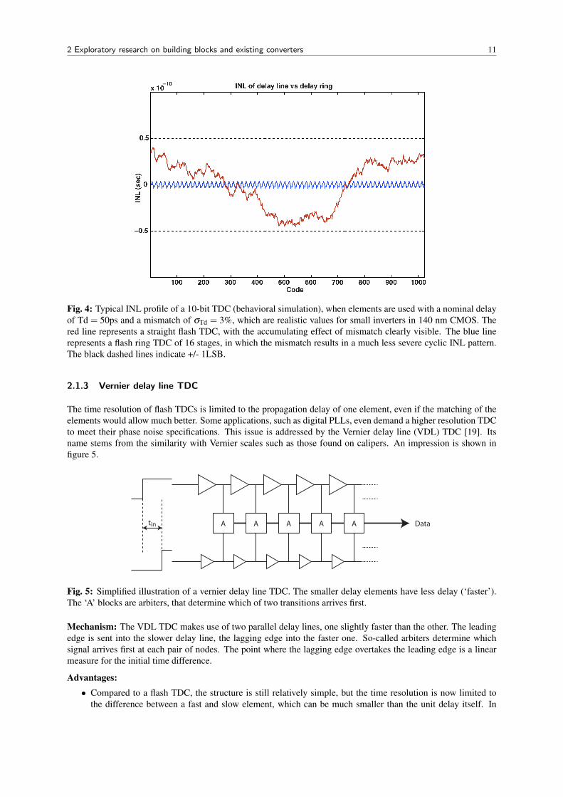
• The mismatch of the delay elements translates to a small cyclic linearity error, as shown in figure 4, insteadof accumulating like in a flash TDC, since the same delay elements are used cyclically.
Limitations:• Like in a regular flash TDC, the time resolution is still limited to a single propagation delay. Also, power
consumption is still limited by the toggling of one delay element for each level. Less flip-flops are required,but a counter is added.
• A ring with a clean start-up behavior is required [22].
• Care has to be taken to load all nodes equally to prevent excessive DNL errors.
• The ring cannot be made extremely short, because the counter has a limited clock frequency.
• If all of these practical issues are covered and the cyclic nonlinearity is sufficiently small, the performancebecomes limited by the accumulating effects of thermal noise on the propagating edge. This means thatsampling rate can be traded for dynamic range in a far greater range than in the regular flash TDC.
2 Exploratory research on building blocks and existing converters 11
Fig. 4: Typical INL profile of a 10-bit TDC (behavioral simulation), when elements are used with a nominal delayof Td = 50ps and a mismatch of σTd = 3%, which are realistic values for small inverters in 140 nm CMOS. Thered line represents a straight flash TDC, with the accumulating effect of mismatch clearly visible. The blue linerepresents a flash ring TDC of 16 stages, in which the mismatch results in a much less severe cyclic INL pattern.The black dashed lines indicate +/- 1LSB.
2.1.3 Vernier delay line TDC
The time resolution of flash TDCs is limited to the propagation delay of one element, even if the matching of theelements would allow much better. Some applications, such as digital PLLs, even demand a higher resolution TDCto meet their phase noise specifications. This issue is addressed by the Vernier delay line (VDL) TDC [19]. Itsname stems from the similarity with Vernier scales such as those found on calipers. An impression is shown infigure 5.
A AA A A Datatin
Fig. 5: Simplified illustration of a vernier delay line TDC. The smaller delay elements have less delay (‘faster’).The ‘A’ blocks are arbiters, that determine which of two transitions arrives first.
Mechanism: The VDL TDC makes use of two parallel delay lines, one slightly faster than the other. The leadingedge is sent into the slower delay line, the lagging edge into the faster one. So-called arbiters determine whichsignal arrives first at each pair of nodes. The point where the lagging edge overtakes the leading edge is a linearmeasure for the initial time difference.
Advantages:• Compared to a flash TDC, the structure is still relatively simple, but the time resolution is now limited to
the difference between a fast and slow element, which can be much smaller than the unit delay itself. In

2 Exploratory research on building blocks and existing converters 12
practice, resolutions of 5 to 10 times below a unit delay can be achieved [19] or even finer resolutions whenthe elements are calibrated [12].
Limitations:• More so than in the flash TDC, matching between the delay elements limits both the resolution and the
dynamic range, as the relative mismatch in a small difference between delay elements is much larger thanthe mismatch of one delay itself. Care needs to be taken to keep the structure monotonic, and to keep thedelay line short enough for sufficient linearity.
• The power consumption is generally larger than in a flash TDC, since twice as many delay elements need tomake a transition for the same number of bits. Furthermore, the more stringent requirements on matching ofdelays may require larger transistors compared to a flash TDC, also resulting in a higher power consumption.
• Resolving the small time differences by the arbiters usually takes long compared to the time steps themselves.Therefore VDL TDCs have a large dead-time to resolve their outputs, recover and prepare for the nextconversion.
2.1.4 Vernier ring TDC
Like the flash TDC, VDL TDCs are not very scalable; to achieve a high dynamic range, long delay lines arerequired and matching starts to impair the linearity. But like the flash TDC, a VDL TDC can be rolled into a ring[23, 24]. The concept is shown in figure 6 for a number of five stages. Interestingly, an early TDC from the 1950swas actually a one-stage Vernier ring TDC made of tubes, called a ‘Vernier chronotron’ [2].
A AA A A Data
Counter
tin
Fig. 6: Simplified illustration of a Vernier ring TDC. The ring oscillator with smaller elements has a higherfrequency.
Mechanism: A Vernier ring consists of two ring oscillators with an equal number of stages, but slightly differentdelays per stage; in this case five stages are shown. The leading edge triggers the slower oscillator, the laggingedge triggers the faster oscillator. In between these events, several oscillations of the slower oscillator may haveoccurred, which are counted to form the coarse data. After the lagging edge arrives, the Vernier principle startsworking until coincidence is detected, yielding the fine data.
Advantages:• This structure is relatively simple, and able to reach sub-gate-delay resolution.
• It features a large dynamic range in a small area.
• The faster ring is only active from the time the lagging edge arrives until it overtakes the leading edge. Thisis beneficial to the power consumption.
• Like in the flash ring TDC, mismatch errors now have a cyclic contribution, and therefore less impact on thelinearity of the TDC.
Limitations:• Even more so than in a flash ring TDC, equal loading of the nodes and low offsets of the arbiters are required
to maintain monotonicity and low DNL.

2 Exploratory research on building blocks and existing converters 13
• If proper measures are taken against the effects of mismatch, thermal noise becomes dominant in the achiev-able dynamic range of this TDC.
2.1.5 Pulse shrinking delay line TDC
The pulse-shrinking delay line TDC [25] is functionally very similar to the VDL TDC. An overview is shown infigure 7.
Data
S S S S S
tin
Fig. 7: Simplified illustration of a pulse-shrinking delay line TDC. The blocks with ’S’-inputs are set-flip-flops(reset not shown).
Mechanism: This TDC consists of a delay line that has different propagation speeds for rising and falling edges.Suppose rising edges travel slower than falling edges. In this case, the leading edge is sent into the delay line asa rising edge, the lagging edge is sent into the delay line as a falling one. A traveling pulse results, that sets SR-latches on its way. As the lagging edge catches up with the leading edge, the travelling pulse vanishes and fails totoggle subsequent latches. The position where this occurs, is a linear measure for the input time difference.
Advantages:• Compared to the VDL TDC, this structure requires only one delay line.
• The delay line has automatically returned to its initial state after the conversion is over; it requires no reset.
Limitations:• This topology requires delay elements with asymmetrical propagation delays. The difference in propagation
delay between rising and falling edges must be well-controlled and well-matched between stages to obtainsufficient linearity.
2.1.6 Coarse-fine TDC
All aforementioned TDCs are fundamentally limited in terms of power consumption, because they require one ortwo delay elements to toggle for each level to be calculated. This can be solved by coarse-fine conversion, anexample is discussed in [9]. An simplified version is shown in figure 8.
Mechanism: This TDC uses a low-power ring oscillator and counter to coarsely digitize the time interval. Afterthe lagging edge has arrived, the counter is read out, and the remainder of that coarse oscillator period is sent to afine TDC, depicted here as a simple flash TDC. If the coarse-to-fine TDC gain is known, the digitized remainder ofthe oscillation period can be used to calculate the fine bits that are appended to the coarse data. The fine convertercan be any one of the aforementioned concepts. In [9], four interleaved flash TDCs are used, but a VDL TDC mayalso be used.
Advantages:• The coarse oscillator can be a relatively slow, low-power oscillator, provided that its jitter will not dominate
the fine conversion.
• The fine converter is only active during one period of the coarse converter, drastically reducing the powerrequired for one conversion.
Limitations:

2 Exploratory research on building blocks and existing converters 14
Coarse data
Counter
Fine data
tin
Edge selector
Fig. 8: Simplified illustration of a coarse-fine TDC. A ring oscillator and counter are used for coarse quantization,a flash TDC is used for fine quantization of the remainder of the last oscillation period (gray area).
• In this structure, especially the coarse-to-fine converter gain needs to be either measured or established. In[9], this is measured by mechanisms that rely heavily on the chaotic locking behavior of the PLL in whichthe TDC is applied. This makes the structure less attractive for use in an ADC.
2.1.7 Time-amplifying TDC
A completely different coarse-fine approach makes use of time amplification [26]. An overview is shown in figure9.
Linear amplification of a time interval can be done using ‘time amplifiers’ (TAs). Such TAs are based on latches;a latch shows an exponentially increasing decision time when the input time difference becomes very small (nearmetastability). Combining the characteristics of two asymmetrical latches yields a region in which linear timeamplification is obtained [26, 27].
A AA A A
A A A
MUX
Coarse data
Fine data
TA TA TA TA TA
tin
Fig. 9: Simplified illustration of a coarse-fine TDC using time amplification.
Mechanism: The time interval is first digitized using a coarse VDL TDC. Meanwhile, all possible ‘time residues’

2 Exploratory research on building blocks and existing converters 15
are amplified using time amplifiers, since time cannot be stored for later use. After the coarse value is deter-mined, the correct ‘time residue’ can be selected using a multiplexer, for fine quantization using a second VDLTDC.
Advantages• Because of the amplification, very fine time resolutions can be achieved using VDL TDCs of modest reso-
lution.
• For N+M bits, only VDL TDCs of 2N and 2M delay elements are needed instead of 2N+M . Because of thesetwo short TDCs, the accumulating effect of mismatch is less severe, so matching requirements are relaxed.Relaxed matching requirements and shorter delay lines are beneficial to area and power consumption.
Limitations:• The structure presents several design challenges: Time amplifiers suffer from gain, offset and linearity prob-
lems much like voltage amplifiers. Although the authors of [26] leverage very clever techniques to monitorand correct these issues, these are not easily adopted.
• This type of TDC requires a large dead time, compared to its full-scale input time. This is necessary for thetime-amplifiers to function and the outputs to stabilize.
2.1.8 Successive approximation TDC
In successive approximation (SAR) TDCs, a binary search is executed to align the leading and lagging edge. Figure10 shows a simplified example.
A
16
Delay by 8,4,2,1
Data
tin
Fig. 10: Simplified illustration of a successive approximation TDC. The depicted loop calculates 5 bits.
Mechanism: The leading edge is delayed by half the full-scale time. An arbiter determines which of the two edgesnow arrives first. The output of the arbiter serves as the most significant bit. The early edge is now delayed by aquarter of the full-scale time and the process repeats. This process is repeated until the achievable number of bitsis reached.
In the form of figure 10, the structure operates in a loop. However, this requires a programmable, binary weighteddelay, along with associated control logic. The loop can also be unrolled to form a less complicated structure, atthe expense of area [28]
Advantages:• SAR TDCs require at least as much total delay to perform their function as flash TDCs (e.g. an ideal 10-bit
SAR TDC still requires about 1024 delays in total), however they are lumped into a delay of 512, one of256, one of 128 et cetera. This can be a practical advantage; details can be found in appendix C.
• The SAR structure can achieve sub-gate delay resolution when the difference in delay between the paths isbelow one gate delay (e.g. one path introduces 1 extra unit delay, the other introduces 1.5 unit delays). Inother words, the finest SAR stages can be Vernier stages.
Limitations:

2 Exploratory research on building blocks and existing converters 16
• In both the cyclic and the unrolled version, the edges need to be ‘held up’ while the arbiters decide whichedge should be delayed for the next decision. To avoid metastability, these ‘buffer delays’ should be quitelong. Any mismatch in these delays will add to the nonlinearity of the system, so some form of calibrationquickly becomes unavoidable.
2.1.9 Oversampling TDC
Certain TDC topologies show noise-shaping behavior, and can therefore be used as an oversampling TDC. Anexample is the gated ring oscillator (GRO) [29], as depicted in figure 11.
Data
Counter
Clock
Z-1
tin
Fig. 11: Simplified illustration of a gated ring oscillator TDC.
Mechanism: The leading edge starts a ring oscillator. A counter starts registering the amount of periods theoscillator makes. At the arrival of the lagging edge, the ring oscillator is stopped and the internal state of theoscillator is registered. The state of the oscillator from the previous sample is subtracted, leaving only the phaseincrease during the current sample.
This method in itself does not yet provide noise shaping. However, when the ring oscillator is stopped by cuttingits power, some charge remains on its internal nodes. This charge represents some excess phase, that was too smallto increase the state of the oscillator by one. In other words, this represents a quantization error. The next timethe oscillator is started, it starts a little ahead of the measured phase, effectively subtracting this quantization error.This mechanism provides first-order noise shaping. Besides this, the inherent element rotation also provides firstorder shaping of the delay mismatches between the ring oscillator stages.
Advantages:• If the technology and the application permits oversampling of the signal, a higher resolution can be obtained
using a GRO TDC.
Limitations:• For correct preservation of the charge, some analog design effort is required to prevent leakage and charge-
injection from degrading the noise-shaping behavior.
Final remarks: The GRO topology is a special case of a ring oscillator switching between two frequencies,one of which is zero. Completely stopping the oscillator has some drawbacks, such as leakage of the chargethat represents the quantization error and start-up effects of the oscillator. These drawbacks are addressed by thedifferential switched ring oscillator (SRO) topology given in [30]. It toggles two oscillators between a high anda low frequency rather than completely disabling them. Two oscillators are used to obtain an overall differentialarchitecture.

2 Exploratory research on building blocks and existing converters 17
Even higher order noise shaping TDCs have already been successfully implemented, for example a 1-1-1 MASHtopology, providing third-order noise shaping [31].
2.1.10 Delay interpolation
One major topic that was not treated in any of the aforementioned concepts is delay interpolation: If sub-gatedelay resolution is desired, but switching to a Vernier concept is too tedious, interpolation of delay elements canbe applied. Examples are using multiple flash TDCs in parallel [8], resistive interpolation [32], or read-out usinginterpolating flip-flops [5].
2.1.11 Quantitative comparison of TDCs
Table 1 gives an impression of the large variety of specifications achievable with the different TDC topologies.Some performance measures are specific to TDCs, others General trends are hard to distinguish, but key parameterssuch as time resolution and figure of merit seem to benefit from technology scaling. Most concepts show a powerconsumption in the order of several mW.
Some authors have started using the Walden figure-of-merit (FoM) to compare TDCs, but the varying amount ofinformation available on the different TDCs makes it hard to do the competition justice. For instance, the FoMsof [32] and [26] are calculated to be 309 and 994 fJ/conversion-step, respectively, by the author of [8], but arefound to be 190 and 2340 fJ/conversion-step, respectively, by the author of [28]. One issue that prevents an honestcomparison is that many TDC topologies show a signal-dependent power consumption. Another is that the varyinginclusion of digital blocks in the power consumption. To prevent speculation based on the varying amount of dataavailable from each publication, only FoMs are shown as calculated by their own respective authors. However, thefew FoMs that are available definitely show potential for use in an ADC.
A remarkably low FoM is that of [8]. Although the topology seems indeed very power-efficient, the FoM is adubious one: It uses both the highest effective number of bits (ENOB) achievable (13.3), and the highest samplingrate achievable (40 MS/s) in the calculation of the FoM. However, the topology cannot achieve these at the sametime: digitizing the full-scale time interval of 90112 ps is physically only possible at 11 MHz or less. Therefore itseems that the actual FoM should be about a factor four higher, at 24 fJ/conversion-step, which is still remarkablyefficient, thanks to the coarse-fine conversion mechanism.
2.1.12 Conclusion on TDC architectures
From this study of many TDC architectures published to date, some general conclusions can be drawn. First,choosing a Vernier topology has little advantages besides sub-gate delay time resolution, and poses many additionalchallenges, so is best avoided when the application does not strictly require sub-gate-delay resolution. This isreinforced by the solution from [8], which achieves a very good figure-of-merit with a relatively easy to implementsolution. The latter also demonstrates that coarse-fine conversion can be key in achieving a good FoM. Finally, thecomparison table shows that TDCs benefit from CMOS technology scaling and state-of-the-art topologies achieveFoMs in a range that is attractive for their use in ADCs.
2.2 Voltage-to-time converters
At the core of any common form of voltage-to-time conversion lies a current-source / capacitance combination,generating a linear ramp, and some form of threshold detector. The difference lies in which variable is controlledby the input voltage. Theoretically, the options are to control the current, the capacitance, the threshold voltage orthe start voltage of the ramp.

2 Exploratory research on building blocks and existing converters 18
Tab.
1:C
ompa
riso
nof
exis
ting
time-
to-d
itiga
lcon
vert
ers
Sour
ce[1
2][2
7][2
6][3
3][3
4][2
9][3
1][3
2]Te
chno
logy
(nm
)90
180
9090
500
130
130
90To
polo
gyV
DL
+m
ism
atch
com
pens
atio
n
Cas
cade
dtim
eam
plifi
erC
oars
e-fin
eV
DL
+tim
eam
plifi
catio
n
Mul
ti-ch
anne
lG
RO
Flas
h+
VD
LM
ulti-
path
GR
O1-
1-1
MA
SHPa
ssiv
ein
ter-
pola
tion
Pow
er(m
W)
--
34.
82.
2-2
11.
73.
6In
putr
ange
(ps)
-13
00(6
0)64
012
500
>37
012
288
1000
0060
1.6
No.
ofbi
ts-
7(6
)9
-11
-7
Res
olut
ion
(ps)
0.88
10.2
(1.0
)1.
2517
306
(1)
N/A
4.7
Sing
lesh
otpr
ecis
ion
(LSB
)0.
421
(8)
0.6
0.08
--
N/A
0.7
Sam
ple
rate
(MS/
s)10
0010
(40)
1040
-50
518
0B
andw
idth
(MH
z)50
05
20-
10.
190
FoM
(pJ/
conv
)-
--
--
0.2
--
Are
a(m
m2)
0.45
0.52
0.6
0.3
0.53
0.04
0.11
0.02
Sour
ce[2
5][3
5][3
6][3
0][2
8][8
][2
3][1
3]Te
chno
logy
(nm
)FP
GA
350
130
9065
4013
080
0To
polo
gyPu
lse-
shri
nkin
gC
yclic
SAR
SAR
Switc
hed
ring
osc
SAR
Coa
rse-
fine
Ver
nier
ring
Cou
nter
+in
-te
rpol
atio
nPo
wer
(mW
)-
331
29.
60.
6-1
.87.
535
0In
putr
ange
(ps)
1150
032
7680
000
1984
2000
-84
0000
1000
090
112
3200
025
0000
0
No.
ofbi
ts8
286
-10
1412
>16
Res
olut
ion
(ps)
421.
2231
--
5.5
832
Sing
lesh
otpr
ecis
ion
(LSB
)1.
332.
620.
28-
0.47
-0.5
90.
81
0.94
Sam
ple
rate
(MS/
s)>
1≤
550
050
-750
8040
15<
0.1
Ban
dwid
th(M
Hz)
>0.
5≤
2.5
250
140
207.
5<
0.05
FoM
(pJ/
conv
)-
--
-0.
230.
006
--
Are
a(m
m2)
N/A
4.45
0.15
0.02
0.11
0.01
0.26
11.9

2 Exploratory research on building blocks and existing converters 19
2.2.1 Current-controlled VTC
Controlling the current of the VTC requires a linear voltage-to-current converter. There are two commonly usedways to accomplish this: the first is a resistor into the virtual ground node of an active integrator, the other is aMOS-based voltage-controlled current source.
Both techniques usually have integrating inputs, in which the input is not sampled, but continuously converted intothe current that is integrated onto a capacitance. This saves the area of a dedicated sampling capacitor. However,since integration corresponds to convolution with a rectangle in the time domain, it yields inherent low-pass filter-ing at the ADC input [15], meaning that such an input stage cannot be used all the way up to Nyquist, and certainlynot beyond (e.g. for IF-sampling). However, the same mechanism does provide useful anti-aliasing.
Active integrator VTC
A simplified overview of an active integrator VTC is shown in figure 12. This configuration is typically used fordual-slope conversion [37]: first, the unknown quantity (Vin) is integrated for a fixed time. Next, a known quantity(Vref) is integrated and the time is measured. A major advantage of this structure is that many circuit imperfectionscancel, such as nonlinearity of the capacitance. Also, the exact frequency of the time base is unimportant, as theratio between the known and measured time directly represents the ratio between the input and the referencevoltage.
Vref
Vin
Reset
Fig. 12: Simplified illustration of an active integrator VTC. Note that for this simplified schematic to be functionalas a dual-slope converter, Vref has to have the opposite sign of Vin.
A disadvantage of this structure is that an op amp has to be constructed, which becomes more problematic asCMOS technology scales.
Voltage-controlled current source VTC
Figure 13 shows a simple VTC in which the current is regulated by the input voltage, in this case a voltage-controlled delay line (VCDL). This example shows that even in a VTC consisting of multiple stages, a currentsource, capacitors and threshold detectors can be distinguished, as stated at the beginning of this section.
Vin
Fig. 13: Simplified illustration of a voltage-controlled current source VTC.
Although this type of VTC can be very simple, obtaining a linear control characteristic of the delays is tedious, an

2 Exploratory research on building blocks and existing converters 20
issue well known from VCO-based ADCs. Digital correction is needed to exceed about 6 bits of linearity withoutmuch analog effort.
2.2.2 Start-voltage controlled VTC
A simplified VTC in which the voltage controls the start voltage of the ramp is shown in figure 14. The start voltageis simply sampled onto a capacitor, after which the capacitor is discharged until the voltage crosses a threshold. Apossible advantage is that the sample is taken and the ramp is generated on the same capacitor. The drawback ofthe depicted implementation is that a current source is needed with a very high output impedance.
Vin I
Sample Slope
Fig. 14: Simplified illustration of a start-voltage-controlled VTC.
2.2.3 Threshold-voltage controlled VTC
In figure 15, a simple threshold voltage controlled VTC is depicted. The input voltage is continuously comparedwith a sawtooth-shaped waveform. The challenges are similar to those in the start-voltage controlled VTC, since asufficiently linear and low-noise sawtooth generator has to be constructed using a current source and capacitor. Ifthe structure is to be used near Nyquist or beyond, a sampler is also required.
Vin
Fig. 15: Simplified illustration of a threshold-voltage-controlled VTC.
2.2.4 Capacitance-controlled VTC
Figure 16 shows a possible implementation of a VTC in which the capacitance is controlled by the input voltage.The capacitances in this case are MOS capacitances, which can be implemented in various ways in practice. MOScapacitances have a nonlinear control characteristic, resulting in a VTC that can be combined only with TDCs ofmodest resolution.
Vin
Fig. 16: Simplified illustration of a capacitance-controlled VTC.

2 Exploratory research on building blocks and existing converters 21
2.2.5 Conclusion on VTC topologies
The four theoretically possible VTC topologies were treated conceptually. Start-voltage and threshold-voltagecontrolled VTCs are the best candidates to achieve good linearity performance with little analog design effort.Current-controlled and capacitance controlled solutions are expected to show modest linearity and are thereforeonly suitable for use with TDCs of modest resolution. Furthermore, a start-voltage controlled VTC has a samplinginput, and can therefore be used up to the Nyquist frequency and possibly for subsampling applications, whereasVTCs with an integrating input provide useful anti-aliasing. A practical advantage of start-voltage controlled VTCsis that the sampling capacitor may be re-used for the slope conversion.
2.3 Analog-to-time-to-digital converters
Only few publications on analog-to-time-to-digital conversion with strictly separated VTC and TDC are availableas of yet. Three examples will be treated next. For completeness, a fourth ADC is treated that occupies a gray areabetween the scope of this work and VCO-based ADCs. The performance figures of the four topologies are listedin table 2 for ease of comparison.
Tab. 2: Comparison of existing analog-to-time-to-digital converters.
Reference [38] [39] [40] [41]
Technology (nm) 180 130 65 65Sample rate (MS/s) 10 80 250 1200Bandwidth (MHz) 0.5 40 20 600SFDR / SNR / SNDR (dB) 66 / ? / 56 ? / ? / 40.6 ? / 62 / 60 30.1 / ? / 20.4ENOB (bits) 9.0 6.45 9.7 3.1Power (mW) 4.5 6.4 10.5 2FoM (fJ/conv-step) 940 920 319 196
2.3.1 Start-voltage controlled VTC and GRO TDC
One implementation is given in [38]. The VTC is implemented as a start-voltage controlled VTC: the input issampled onto a capacitor, which is then discharged through a cascoded current source. The threshold detector isimplemented by a single transistor toggling a regenerative latch. This way, the generated edge is already sharpafter the first stage of the threshold detector, improving its linearity. The TDC is a gated ring oscillator, and tobenefit from its noise shaping, the overall ADC is oversampling by a factor of 20.
The performance figures for this ADC are based on a post-layout simulation.
2.3.2 Start-voltage controlled VTC and two-step TDC
Another example is [39]. The VTC is again implemented by sampling the input voltage onto a capacitor anddischarging it through a triple cascoded current source. The TDC is a two-step TDC, comprising a simple oscillatorand counter for coarse quantization, and a multi-path GRO for fine quantization with sub-gate-delay resolution. Inthis case the oscillator is used at Nyquist, so there is no benefit from noise shaping.
2.3.3 Start-voltage controlled VTC and flash TDC in sigma-delta ADC
Another publication worth mentioning is [40], which uses the whole structure of VTC and TDC combined as aquantizer in a sigma-delta ADC. The VTC is an asymmetrical pulse-width modulation (PWM) block, which mostclosely resembles the ‘threshold-voltage controlled VTC’ from the previous section. The TDC is a flash TDC thatmeasures the pulse width from the PWM. It also regenerates the discretized pulse to be fed back to the sigma deltaloop filter.

2 Exploratory research on building blocks and existing converters 22
2.3.4 Voltage-controlled delay-line based ADC
The last work to be mentioned here is that of [41]. The input voltage is sampled differentially and converted todifferential control currents for two delay lines. The difference in propagation speed between the two delay linesdetermines the output code.
Technically, the voltage-to-time and time-to-digital converter are not separate blocks in this architecture: it is avoltage-controlled delay line (VCDL) architecture, placing it outside the scope of this research. However, thework contains useful discussions on noise and mismatch and does show the feasibility of highly digital, time-basedarchitectures.
2.3.5 Conclusion on analog-to-time-to-digital topologies
Two ADC topologies that fit the scope of this thesis make use of a start-voltage controlled VTC, the third makesuse of a threshold-voltage controlled VTC. This fits the conclusions from the study of VTC architectures. Althoughthe number of studied publications is low and there are large differences in implementation, for the four examplesthe converter FoM gets better with newer CMOS technology. Also, gated ring oscillators are a popular choice forimplementing the TDC.
2.4 Summary
The study of existing TDC architectures led to some general conclusions. Key points to keep in mind are thatit is possible to keep the structure simple if the application does not strictly require sub-gate-delay performance.Coarse-fine conversion can be key to a good figure of merit of the TDC.
The possibilities for the VTC were explored more conceptually. The start-voltage or threshold-voltage controlledVTC are good candidates to achieve high linearity with limited analog design effort. This is reinforced by the factthat three previous publications that fit the scope of this thesis, also make use of these types of VTCs.

3 System-level design of the analog-to-time-to-digital converter 23
3 System-level design of the analog-to-time-to-digital converter
This section outlines and motivates the choices made on system level. A TDC topology is chosen, armed with theknowledge from previous work. Next, a VTC topology is determined, and the interactions between TDC and VTCare discussed. The section concludes with a block diagram of the proposed system.
3.1 TDC topology
In choosing a TDC topology, an important realization was that the overall system would be an ADC, with no cleartarget specification but to make optimal use of the advantages of time-domain quantization. This puts no cleartarget requirements on the TDC, in contrast to the use of a TDC in a PLL, for example, where the required TDCresolution follows from phase noise requirements, and the required dynamic range follows from the desired rangeof output frequencies and the range of the feedback divider [5].
So basically all TDC options were open, and a choice needed to be made for a TDC that fit an easily implementable,highly digital, small, reconfigurable and power-efficient ADC topology.
A flash ring TDC turns out to meet most of these criteria. The simplified schematic is repeated in figure 17. Itconsists of a ring oscillator that can be started by the leading edge, a coarse counter that keeps track of the numberof cycles the oscillator has made, and flip-flops to register the state of the oscillator for fine resolution.
Data
Counter
tin
Fig. 17: Simplified illustration of a flash ring TDC.
A flash ring TDC is:
• Easily implementable: of all TDC topologies, it poses the most relaxed demands on matching of delay ele-ments. For one, because it does not attempt to achieve sub-gate-delay resolution, and also because mismatcherrors are turned into a cyclic pattern. These relaxed demands on matching of delays make this topologyvery robust to future technology scaling.
• Highly digital: it does not require the design of arbiters, as required in Vernier- or SAR-like topologies.
• Small in area: the ring can be made as short as allowed by the maximum operating frequency of the coarsecounter.
• Reconfigurable: By adding an extra bit to the coarse counter and allowing twice as much time for theconversion, the dynamic range is doubled. Since the mismatch error turns into a cyclic pattern of much lessthan an LSB (as shown in figure 4 in section 2.1.2), this fact can be exploited until the effects of thermaljitter or low-frequency noise become dominant.
However, this type of TDC has one major drawback: Its power consumption is fundamentally limited to the tog-gling of one delay element for each level. As mentioned previously, one solution is to use coarse-fine quantization,but for this to work, the coarse-to-fine TDC gain has to be either known or well-established. If the TDC is ap-plied in a PLL, an estimate of the coarse-to-fine gain can be made because the chaotic locking behavior of thePLL will eventually hit all the fine codes [8], but in an ADC, the value has to be known regardless of the signalstatistics.
This work introduces another way to save power, resulting from the fact that this work is about an ADC, notjust a TDC. If the TDC is a ring, that is only read out, but not interrupted for each conversion, it can be usedfor multiple AD-conversions in parallel. In other words, multiple VTC ‘channels’, operating in parallel, will be

3 System-level design of the analog-to-time-to-digital converter 24
mapped onto one uninterrupted TDC. This way, the power consumption of the TDC can be divided over multipleconversions.
Now, a flash ring TDC that cannot be interrupted for each conversion reduces to nothing but a continuously runningring oscillator, the state of which is sometimes read out. The remaining issue is how to synchronize this oscillatorwith the incoming time-samples. This can be done in multiple ways:
• register the state of the oscillator at both the leading and lagging edge, and subtract the two values from eachother
• force the leading edge to occur when the oscillator is in a known state, so only a snapshot of the state at thelagging edge is needed
The latter option is the most attractive, as it requires only one set of flip-flops to register the state of the oscillator,and less complex digital decoding. The remaining question is how to synchronize the oscillator with the leadingedge in practice, but to answer this, first a voltage-to-time topology had to be chosen.
A final note about the TDC ring oscillator is that, to simplify the digital backend, it would be most convenient ifthe number of stages were a power of two. It will be shown later that with the right oscillator topology, this isindeed possible.
3.2 VTC topology
The qualitative comparison of possible VTC topologies in the previous section revealed that an attractive option isto sample the input voltage on a capacitor, then discharge the capacitor using a fixed current. A threshold detectorgenerates the output signal.
Ensuring the linearity of such a VTC is relatively easy. Also, it uses the same capacitor for sampling and generatingthe slope, possibly saving area. Also, its sampling nature makes it operable up to Nyquist and beyond. Allaforementioned publications on analog-to-time-to-digital converters made use of this type of VTC.
The drawback of this topology is that a current source with a very high output impedance is required to keep thecurrent constant while the voltage across the capacitor is dropping. This is hard to implement with small transistorsand little voltage headroom. However, the implementation chapter of this work describes a way to overcome thisissue. Therefore a sampling, start-voltage controlled VTC was chosen. This fact is used in the remainder of thissection.
3.3 Integration of TDC and VTC
To integrate TDC and VTC to form an ADC, the issue still had to be addressed of how to force the leading edge tooccur when the TDC is in a known state. This can be done in two ways:
• a synchronous way: lock the TDC ring oscillator to the ADC sampling clock using a PLL. Then start thevoltage-to-time conversion simply using the sample clock.
• an asynchronous way: let the TDC remain a a free-running ring oscillator. After the input sample is taken,let the TDC indicate when it reaches a known state, and start the voltage-to-time conversion at that instant.The clue here is that the VTC does not necessarily have to start directly after the sample has been taken.
Implementing a PLL requires designing a phase/frequency detector, a loop filter and a charge pump (or, in case ofa digital PLL, an additional TDC, digital loop filter and DAC). All of these consume area and power, and requireanalog design effort. Besides this, most ways of making the oscillator tunable tend to slow it down, degrading theTDC time resolution. Therefore, a free-running ring oscillator will be used for the TDC in this work. So, after thesample has been taken, further timing of the VTC is controlled by the TDC, as illustrated in figure 18.
The drawback of this approach is that the frequency of the ring oscillator will be unknown and varying (due to pro-cess, supply and temperature variation and flicker noise). Therefore, additional measures are required to guaranteethe TDC gain and accuracy. Both issues were addressed on ADC-level by a reference conversion mechanism, asdiscussed next.

3 System-level design of the analog-to-time-to-digital converter 25
Time
VTC TDC
Tracking
Holding
... performing ramp ...
Idle oscillation
Known state
... oscillating and counting...
Thresholdcrossed Register coarse
and ne bits
Sample clock
“VTC is ready”
Holding“Start conversion”
“Done” +-
+Output
Fig. 18: Interaction between the VTC and asynchronous TDC. The ADC sample clock switches the VTC fromtrack to hold mode. Timing of the conversion is governed by the asynchronous TDC.
3.3.1 Reference conversion
The final issue to be resolved was how to fix the gain of the ADC over process, voltage and temperature variations.The proposed solution is to periodically sample and convert a reference voltage, next to the input voltage. Sucha reference conversion can be used in various ways to either measure or fix the full-scale value of the ADC. Ifproperly applied, it compensates for slow variations in gain in both the VTC and the TDC.
If nothing would be done to use this reference voltage, the waveforms in the VTC would be as depicted in figure19. At Tstart, the VTC starts integrating the reference or input voltage with an arbitrary slope. This results in twozero-crossing events, Tstop1 and Tstop2. Tfull-scale represents the full-scale time of the TDC (e.g. for a 10-bit TDC,it represents 1024 unit delays). Note that for clarity, the conversion of Vin and Vref are depicted as if taking placesimultaneously, but this is not necessarily true.
Vref
Vin
0
Slope = I/C
Tstart Tstop2
Tfull-scaleTstop1
time
volta
ge
Fig. 19: Waveforms and important timing points in a sampling VTC, converting an input and a reference voltage,if no further measures are taken.
There are a few practical ways to obtain useful output from such a VTC. One way is to do nothing more, and justfeed Tstop1-Tstart and Tstop2-Tstart to a digital divider, as depicted in figure 20.
Another option to fix the ADC gain is to ensure that Tstop2-Tstart = Tfull-scale, by adjusting the slope, as depicted infigure 21. This can be done using a first-order locked loop that locks the Tstop2 zero-crossing to an edge that isgenerated when the TDC reaches Tfull-scale.

3 System-level design of the analog-to-time-to-digital converter 26
0
Slope = I/C :time
volta
ge
Vref
Vin
Tstart Tstop2Tstop1
Fig. 20: Waveforms and important timing points the VTC, if no further measures are taken and digital division isused to obtain an output value.
Vref
Vin
Tstart Tstop2Tstop1
0
Slope = I/C
Tfull-scale time
volta
ge
Fig. 21: Waveforms and important timing points in the VTC, if the slope is tuned to make Tstop2-Tstart equal toTfull-scale.

3 System-level design of the analog-to-time-to-digital converter 27
A third option is to do the same, but by adjusting the speed of the oscillator, as shown in figure 22. This can bedone in much the same way, again using a first-order loop.
0
Slope = I/C
Tfull-scale time
volta
ge
Vref
Vin
Tstart Tstop2Tstop1
Fig. 22: Waveforms and important timing points in the VTC, if the oscillator is tuned to make Tstop2-Tstart equal toTfull-scale.
Another solution is to let the reference slope run for Tfull-scale and retain the end voltage, Vend. If the input rangefrom 0 to Vref is ‘compressed’ into the range Vend to Vref, the input range is mapped onto the TDC range. Thissituation is depicted in figure 23.
0
Slope = I/C
Tfull-scale
volta
ge
Vref
Vin
Tstart Tstart2Tstop2 Tstop1
Fig. 23: Waveforms and important timing points in the VTC, if the input range is scaled to use Tfull-scale.
In this work, the first option is used: a digital division of Tstop2 and Tstop1. Division will be performed off-chip, aswell as generation of the reference voltage, to keep the prototype simple and versatile. This way, also the absolutevalues of Tstop1 and Tstop2 will be available, and experiments can be done using different types of rounding afterdifision.
This option does have some drawbacks: Ffirst, digital division is a sequential process, and therefore not trivial toimplement. Second, both Tstop1 and Tstop2 need to be digitized using the TDC. Third, the accuracy after divisionand rounding has to be sufficient for the desired number of bits. This at least requires Tstop2-Tstart to be guaranteedto be larger than Tfull-scale. A more thorough investigation of the implications of digital division may be necessary,but was not performed within this thesis.
3.4 System overview
Figure 24 shows an overview of the proposed system, with all architectural choices incorporated, except for thereference sampling mechanism, this is omitted for clarity.
The time base of the TDC is shown in the bottom left. It consists of the oscillator, its output buffers and the coarsecounter. The section surrounding it, inside the dashed L-shape, is one VTC ‘channel’ and its associated part of theTDC.

3 System-level design of the analog-to-time-to-digital converter 28
VinStop
Sample
SampleStop VTC_Ready
Coarse dataCounter
Stop
Start
Thermoto
Binary
+-
+
Fine data
Start
VTC channel (n) Digital backend (1 or n)
Start
Ramp
Vstop
Count_start
Count_end
Ringosc, buers and counters (1)
Fig. 24: Architectural overview of the proposed system.
It is assumed that the sample is taken on the falling edge of the sample clock. If both the sample clock and the ‘stop’signal are low, indicating a sample has been taken, but the conversion still has to take place, the VTC generatesa ‘VTC ready’ signal. This signal is synchronized to the oscillator by a flip-flop to form a ‘Start’ signal. On thissignal, the output of the coarse counter is registered and the VTC starts the ramp.
Once the ramp crosses the threshold, the ‘Stop’ signal is generated by the VTC. This signal is used to record thecoarse counter output and the state of the oscillator.
The digital back-end subtracts the counter end value from the start value to yield the coarse bits. The state of theoscillator is decoded to binary. Since the stages in the oscillator were assumed a power of two, the fine bits cansimply be appended to the coarse bits, and no adjustments are needed to the coarse or fine bit values.
3.4.1 Metastability
The architecture as shown in figure 24 suffers from two metastability issues.
The first is when the ‘VTC ready’ signal violates the set-up and hold requirements of the flip-flop that generatesthe ‘Start’ signal. To solve this, the single flip-flop is replaced by a standard two-flip-flop synchronizer.
The second issue occurs when the stop edge arrives. Possibly, the measured state of the oscillator is a low value(e.g. 0 or 1), indicating that the coarse counter should have just been incremented. However, maybe the coarsecounter has not noticed that ‘edge’ yet. Then, an error of one coarse bit is generated.
Two solutions are known for this issue: in [8], the coarse counter is decoupled from the ring and a regenerativelatch regenerates the last known value at the counter clock input. This value is used to determine if the counter hasjust counted (and therefore the fine bits should be low), or if the counter is about to count (and therefore the finebits should be high). However, decoupling the coarse counter from the ring means that one counter is required forevery VTC channel.
Another solution is given by [14]. This work uses two counters on opposite phases of the oscillator. The fine bitsare used to select the coarse counter that should be stable. A small post-correction to the chosen value is required,based on the fine bits. This solution is much more appropriate for our purposes, since the two counters can bere-used for every VTC channel.
Figure 25 shows the system overview again, now incorporating the two measures against metastability.

3 System-level design of the analog-to-time-to-digital converter 29
VinStop
SampleSample
Stop VTC_Ready
Coarse data
Counter
Counter
Stop
Start
FineMSB
Mux+
-
-+
Fine data
Start
VTC channel (n) Digital backend (1 or n)
Start
Ramp
Vstop
Thermoto
Binary
Count_start
Count_end_1
Count_end_2
Ringosc, buers and counters (1)
Fig. 25: Architectural overview of the proposed system with added measures against metastability.
3.5 Target specifications
To implement a proof of concept, a target resolution had to be chosen. Based on the TDC alone, many bandwidth-resolution combinations can be targeted, so the choice needed to be based on what is achievable with the chosenVTC topology.
Since the ‘sample-and-ramp’ VTC-topology was chosen because the linearity of V-to-I converters is generallylimited to 6 bits or so, it makes no sense implementing a converter for 6 bits or less. On the other side, choosingmore than 12 bits requires excessively large sampling capacitors [42], which negates the advantage of the ADCcore being very digital and small.
Therefore, a resolution of 10 bits was targeted. To exploit the reconfigurability of the time-based ADC concept,one 10-bit VTC channel will be constructed such that it can also operate as multiple interleaved channels at lowerresolution.

4 Implementation of the analog-to-time-to-digital converter 30
4 Implementation of the analog-to-time-to-digital converter
This section describes the steps taken toward a transistor-level proof-of-concept design of the ADC.
Despite the fact that the ADC concept was designed to maximally benefit from newer CMOS technologies, theproof of concept was implemented in NXP’s mainstream 140 nm CMOS process.
The design of the TDC and VTC are highly intertwined, making it difficult to fully separate the discussion of theirimplementations. Nonetheless, first the implementation of the TDC will be discussed, followed by the implemen-tation of the VTC.
4.1 TDC
While determining the system level architecture, the choice was made to implement the TDC as a flash ring TDCthat operates uninterrupted and asynchronous to the sampling process. This reduces the design of the TDC to aring oscillator with appropriate flip-flops or latches to determine its state, and some digital post-processing.
4.1.1 Ring oscillator
As mentioned during the system-level design, an oscillator is desired of which the number of stages is a powerof two, implying an even number of stages. Such oscillators with an even number of stages generally have astable latch-up state, which has to be suppressed to achieve oscillation. Several oscillator types exist that have aneven number of stages, mainly because they are useful for quadrature signal generation. Most frequently used arecurrent-mode logic oscillators and standard CMOS inverter oscillators with weak cross-coupled latches.
Current-mode logic (CML) oscillators have some advantages, such as high power-supply rejection [43]. However,they are not very suitable here because the stages draw a continuous current. In our topology, quite a lot of stagesare needed to slow the oscillator down to a suitable rate for the coarse counter, so a CML oscillator would consumea lot of static power. Also, CML oscillators have low-swing output signals, which are not convenient in a highlydigital system.
Simple CMOS inverter rings with weak cross-coupled inverters [43] do have full-swing outputs and consume littlestatic current per stage. One problem with these oscillators is that the sizing of the weak inverters relative tothe main inverters is rather critical: strong inverters make the oscillator power-hungry, and weak inverters do notprevent latch-up.
A more suitable oscillator was found in a front-end for ultra-wideband radio [44]. A schematic of one stage isshown in figure 26. Its inner workings are quite straightforward: MP1/MN1 and MP2/MN2 form two inverters.MP3/MN3 and MP4/MN4 prevent the outputs of the stage from changing if the inputs are not in antiphase, thusensuring oscillation. This oscillator stage does not consume static power and has full-swing outputs. Under normaloperating conditions, the cross-coupled transistors can be considered cascode devices, which is beneficial for noiseand power consumption.
Early performance estimates of the oscillator and counter showed that an 8-stage, 16-phase oscillator would be thesmallest power of 2 to leave sufficient timing margin for the counter to operate. Therefore, an oscillator of 8 timesthe depicted stage was adopted. The 16 output phases of the oscillator were buffered using unit inverters from thedigital library.
As a starting point for the size of the transistors in the oscillator stage, all NMOS transistors were sized equal tothose inside a minimal digital gate with two stacked NMOS transistors, such as a NAND gate, i.e.0.856/0.16µm.This was considered a good starting point for a small, power-efficient oscillator, since the oscillator stages can alsobe considered digital gates with a limited fan-out: each stage will drive the next stage and a minimal inverter usedas an oscillator output buffer. The PMOS transistors were also chosen minimum length, and their width was sweptwhile observing the oscillator phase noise. From a W/L of 2.6/0.16 upward, no further improvement in phase noisewas observed, so this width was kept. Increasing either the four transistors M1-2 or the four transistors M3-4 whilekeeping the others at the same size did not improve the phase noise performance of the oscillator any further. Theresulting phase noise after the output buffers is shown in figure 27.

4 Implementation of the analog-to-time-to-digital converter 31
MP1 MP2
MN1 MN2
MP3 MP4
MN3 MN4
IN+ IN-
OUT+OUT-
Fig. 26: Schematic of the differential oscillator stage.
Phas
e no
ise
(dBc
/Hz)
Relative frequency (Hz)
Fig. 27: Phase noise plot of the optimized 16-phase, 8-stage oscillator, with unit inverters as output buffers and nofurther loading, measured after the output buffers.

4 Implementation of the analog-to-time-to-digital converter 32
To verify if the oscillator is power-efficient compared to other ring oscillators, the oscillator FoM was calculated,defined as [45]
FoM = L ( ff-2)(ff-2
fosc
2)
Pcore
1mW(1)
where fosc is the oscillator frequency, ff-2 is an offset frequency from fosc where the upconverted thermal noisedominates, L ( ff-2) is the phase noise at this offset frequency, and Pcore is the power consumption of the oscillatorcore. Good ring oscillators come within 6 dB to the theoretical FoM limit, which lies at -165dBc/Hz at a tem-perature of 290K [46]. Simulations show that the oscillator designed above oscillates at 689 MHz with a phasenoise of -126 dBc/Hz at 10 MHz offset, while the core (excluding output buffers) consumes 475 uA from the1.8V supply. This results in a FoM of -164 dBc/Hz, which is very close to the theoretical limit, indicating thatthe oscillator design is good, even if some dB’s of performance are lost due to parasitics later. The oscillator coreachieves a nominal propagation delay of td,nom = 90.7 ps per stage, and requires 78 fJ per propagation step. Thisis an indication of the achievable time resolution and FoM of the TDC, however, both specifications will worsenwhen parasitics are included. Furthermore, the power consumption in the proposed architecture will be dividedover the number of VTC channels that will be using the TDC simultaneously, resulting in a division of the FoM bythe number of channels.
The variance in delay of a single stage due to thermal noise can be calculated from the phase noise in the thermalregion [47]:
σtd,thermal =ff-2
fosc·10
L ( ff-2)20 ·
√td,nom (2)
resulting in σtd,thermal = 69 fs, or about 0.077%. This is equal to the thermal period jitter of one oscillator outputphase, divided by
√16, since the oscillator has 16 stages.
In section 2, the statement was made that generally, the effects of thermal jitter generally lie about an order ofmagnitude below those of mismatch jitter. To verify that statement for the oscillator at hand, mismatch simulationswere also executed. A 100-point Monte-Carlo simulation of the oscillator showed a standard deviation in the delaysof σtd,mismatch = 2.43ps or 2.7% (excluding mismatch in the output buffers). Therefore, for this specific oscillatorstage, the effects of thermal noise lie about a factor 35 below those of mismatch.
As demonstrated in section 2, using a ring TDC turns mismatch errors into a cyclic INL pattern of a low magnitude.The remaining INL profile is comparable to that of a short delay line of 16 stages, repeating itself. The standarddeviation of the maximum point of this INL pattern can be estimated by [48]:
σINL,max =
√N4
σtd,mismatch
td,nom(3)
Inserting N= 16 stages, σtd,mismatch = 2.43ps and td,nom = 90.7ps, σINL,max = 0.054LSB. Therefore, the mismatchjitter will not limit the performance of this TDC, and the number of bits that can be calculated becomes dominatedby the thermal jitter. A quick calculation shows that an edge should propagate through about 430000 of thesestages to develop half a unit delay (half an LSB) of thermal jitter. In other words, theoretically a TDC of morethan 18 bits could be constructed using the proposed oscillator, however, at such lengthy propagation times, other(low-frequency) effects will start influencing the propagating edge, such as supply voltage and temperature driftand flicker noise.
Timing
Since the TDC will be running asynchronously, measures need to be taken to guarantee sufficient accuracy of theconverter under all process, voltage and temperature conditions. At slow conditions for the oscillator, a TDC LSBbecomes longer, so the TDC can calculate less levels per second. Therefore the amount of time the TDC needs tomake 210 = 1024 time steps under the slowest conditions dictates the full-scale output of the VTC.
For reasons that will be detailed in section 4.2.1, the VTC will be configurable to act as either one channel with10-bit performance or four channels with 9-bit performance. In this 9-bit mode, the full-scale time from the VTCshould cover 512 of the slowest possible time steps from the TDC.

4 Implementation of the analog-to-time-to-digital converter 33
The slowest oscillation conditions are defined here as the slow process corner, with 10% reduced supply voltageand a temperature of 80 C. Simulations show that under these conditions, the delay per stage increases to 147 ps.For the calculation of 10 bits, the full-scale input time would then be 1024 ·147 ps = 150.5 ns. For the 9-bit mode,the full-scale time is 75.3 ns.
Besides time for the ramp, the time required for conversion should also include the 16 to 32 time steps required bythe synchronizer to generate the ‘Start’ signal from the the ‘VTC ready’ signal (refer to figure 25). At the sameslow conditions, this equals 2.35 - 4.70 ns. Finally, some margin has to be included for additional delay from thecomparator toggling to the instant the oscillator state is sampled.
The prototype will be clocked by the same clock signal in both 10-bit and 9-bit modes. Table 3 illustrates howthe converter operates from this clock signal in both modes. In 10-bit mode, the VTC requires one clock cyclefor sampling and two for slope conversion, whereas in 9-bit mode, all four channels require one clock cycle forsampling and one for slope conversion.
For 10-bit conversion, the slope phase takes 150.5 + 4.7 = 155.2 ns plus margin, for 9-bit conversion it takes 75.3+ 4.7 = 80 ns plus margin. Therefore, a master clock of 11 MHz will be used, resulting in cycles of 90.9 ns, giving10.9 ns margin in 9-bit mode and 26.6 ns margin in the 10-bit mode.
Tab. 3: Timing of the converter when the VTC is operating as a 10-bit channel or as four interleaved 9-bit channels.
Cycle 1 2 3 4 5 6 7
10-bit Sample Vin Slope Sample Vref Slope
9-bit, ch1 Sample in Slope Sample ref Slope9-bit, ch2 Sample in Slope Sample ref Slope9-bit, ch3 Sample in Slope Sample ref Slope9-bit, ch4 Sample in Slope Sample ref Slope
Besides the slowest oscillation conditions, the fastest oscillation conditions are also important: these determine,together with the synchronizer, the minimum time between the ‘VTC ready’ signal and the ‘Start’ signal for theslope, in other words how much time there is available for the VTC to prepare for the slope after the input sampleis taken.
The fast oscillation conditions are defined as the fast process corner, combined with 10% increased supply voltageand a temperature of −20 C. Under these conditions, the propagation delay of a stage is only 64.8 ps, correspond-ing to an oscillation frequency of 965 MHz. In case of a two-flip-flop synchronizer, the VTC has at least oneoscillation period available, or about 1 ns. Should this be too little, then the synchronizer can be extended withmore flip-flops, each one adding one oscillation period of about 1 ns to the time the VTC has available. Care hasto be taken that this time does not exceed the margins that were included in the sampling period under the slowestoscillation conditions.
4.1.2 Digital backend
To register the state of the oscillator and counters, and translate the results into a binary code, appropriate flip-flopsand some digital circuitry are required. The implementation of these blocks is discussed next.
Flip-flops
Since the outputs of the oscillator are 16 full-swing signals, they could theoretically be sampled using flip-flopsfrom the digital library. To find out if this is indeed possible or if more sophisticated, custom flip-flops need to bedesigned, the expected shortcomings of library flip-flops were listed for further investigation:
• Metastability
• Mismatch of the input threshold
• Mismatch in timing path from clock to sampling instant

4 Implementation of the analog-to-time-to-digital converter 34
• Kickback
• Loading of the oscillator
• History effects
• Power supply rejection
Metastability is not expected to be an issue: although the flip-flops sample a high-frequency signal on a criticalclock edge, they are given a significant portion of the (much slower) sampling period to regenerate their outputsafterwards.
To find out if mismatch would cause trouble, the digital library flip-flops were put on a test bench, depicted infigure 28, and subjected to Monte-Carlo simulations while sampling a full-swing transition. The test bench useslibrary inverters to provide realistic transitions on the clock and data inputs of the flip-flop. The clock input isan unfiltered transition from a unit inverter, whereas the data input is an edge that is slowed down using somecapacitance, to have a rise time of about 90 ps. This signal imitates the unbuffered output of the oscillator, andserves as a worst-case signal for the flip-flop to sample. Mismatch contribution of the inverters and capacitors wasexcluded from the simulation, to ensure that only the effect of the flip-flop itself is studied.
Fig. 28: Test bench used to test the mismatch of library flip-flops. Only the flip-flop itself is set to contributemismatch.
The result is shown in figure 29. A cumulative distribution function was fit to the results using MATLAB, todetermine the standard deviation, which turned out to be 3.19 ps, or about 3.5% of the nominal delay. In otherwords, using library flip-flops in the TDC would contribute about 0.035 LSB RMS to its DNL, so no problems areexpected due to poor matching of library flip-flops.
To check if kickback and loading would cause trouble, a bank of flip-flops was connected to the oscillator. Threeoutput periods of the oscillator were compared: one where the flip-flops were ’tracking’, one where the flip-flopswere switched from ‘tracking’ to ‘holding’ halfway the period, and one where the flip-flops were ‘holding’. Therewas no noticeable deviation in length between these three periods, indicating sufficient isolation between oscillatorand flip-flops. If isolation problems are expected after including parasitics, the isolation between oscillator andflip-flops can always be improved by using two or more cascaded buffers.
History effects were not studied extensively, but can always be prevented by using flip-flops with a reset input, ifnecessary. Power supply rejection of library flip-flops was also not studied further, but may be worth investigat-ing.
All in all, no severe problems are expected when simple library flip-flops are used in the TDC.
Decoding logic
The output of the oscillator has the form of a ‘travelling pulse’: at any given time, half of the outputs will be logichigh, and half will be logic low. This pattern cycles through the oscillator. To decode such a pattern into the finebinary code, the structure of figure 30 is proposed. It consists of mostly inverting logic, since such gates are smallerand faster than non-inverting gates.
A bank of NAND gates with one inverting input is used to find the transition from 0 to 1. This results in a zeroat the location of the transition, comparable to ‘one-hot’ coding. In normal one-hot coding, a tree of OR-gates isused to convert the position of the ‘1’ to a binary representation. In this case, a variation of the OR-tree is used,consisting of only inverting gates, to convert the position of the ‘0’ to binary. Because of the inherent monotonicityof the TDC, no bubble correction is expected to be necessary.

4 Implementation of the analog-to-time-to-digital converter 35
3.36 3.38 3.4 3.42 3.44 3.46 3.48 3.5 3.52 3.54x 10⁻¹⁰
0
0.1
0.2
0.3
0.4
0.5
0.6
0.7
0.8
0.9
1
Clock delay (sec)
Prob
abilit
y of
pos
itive
out
put
INL of delay line vs delay ring
Mismatch simulationsbinomial distribution fit
Fig. 29: Probability that a flip-flop will sample an edge as a positive input, as a function of a delay in the clocksignal, under influence of mismatch. The absolute value of the clock delay is arbitrary. For each point, 100Monte-Carlo runs were executed.
Fig. 30: Decoding logic to extract fine binary code from the oscillator state. The signals ‘X or Y ’ are outputs ofanother NAND gate combining X and Y .

4 Implementation of the analog-to-time-to-digital converter 36
Counter
To keep track of the coarse bits, two synchronous counters are required on opposite output phases of the oscillator.The fine bits are used to select the counter that has a stable output, thus preventing metastability.
If the TDC full scale would always be 1024 time steps, or 1024/16 = 64 oscillation periods (in 10-bit mode), a6-bit counter would be sufficient. However, this is only true for the slowest oscillation conditions. To cover alsothe faster oscillation, the counter needs some additional bits. Since the fastest conditions are slightly more thantwice as fast as the slowest conditions, two extra bits are needed.
The 8-bit counters were implemented as shown in figure 31. The counters have a reset input, which is needed tosynchronize them when the converter is started. Synchronized counters are required because if counter 1 togglesfrom e.g. 50 to 51 at a certain edge from the oscillator, counter 2 also has to toggle from 50 to 51 half an oscillationperiod later to obtain a coherent range of output values.
The proposed counter circuit was tested to function correctly at close to 2 GHz under nominal process conditions.It consumes on average 232µW when clocked at the nominal oscillation frequency of 689 MHz.
Q
QSET
CLR
D
Q
QSET
CLR
D
Q
QSET
CLR
D
Q
QSET
CLR
D
Q
QSET
CLR
D
Q
QSET
CLR
D
Clock
Reset
Bit1 (LSB) Bit2 Bit3 Bit4 Bit5 Bit6
Q
QSET
CLR
D
Q
QSET
CLR
D
Bit7 Bit8 (MSB)
Fig. 31: Implementation of the 8-bit synchronous counter.
Remainder of the digital backend
The remainder of the digital backend consists of:
• selecting the stable counter based on the fine code
• correcting the value based on the MSB of the fine code
• subtracting the initial counter value to obtain the digital output
• performing digital division of the input sample by the reference sample
These blocks were not implemented further: the proposal is to let the proof-of-concept output the ‘raw data’ fromthe flip-flops and thermo-to-binary decoder and perform the listed post-processing steps off-chip.
4.2 VTC
This section discusses the step-by-step implementation of the voltage-to-time converter. First, a start-voltagecontrolled VTC mechanism is proposed and after the dominant noise sources have been identified, the componentsare sized.
4.2.1 Sample and ramp circuit
To generate a very linear ramp on a capacitor, a high-impedance cascoded current source can be constructed [38–40], but this is not a very technology-scaleable solution. Feeding the current into a virtual ground node puts much

4 Implementation of the analog-to-time-to-digital converter 37
less requirements on the current source. However, constructing a complete op-amp to implement a virtual groundis not a very portable solution either.
The proposed solution is to sample the input voltage on a capacitor, then connect the capacitor across a single-transistor OTA. This OTA provides a virtual ground for the current source, but also re-uses the current through thecapacitor to bias itself. This technique has recently been succesfully applied in a low-power relaxation oscillator[46]. The mechanism is illustrated in figure 32.
MN1Vin
Vin
+-
+-
+-
VOTA
Ibias
C
VOTA
Tstart Tstop
Vin+VOTA
MN1VOTA
Ibias
+-
VC+VC-
VC+
Fig. 32: Operation principle of the VTC.
During the sampling period, the OTA transistor MN1 is connected as a MOS diode. The diode voltage is alsothe virtual ground voltage of the OTA, or VOTA. After sampling, the capacitor is stacked onto this diode voltageand given some time for the voltage levels to shift. Now, the VTC is waiting to start the linear ramp, and on the‘Start’ signal from the TDC, the diode is opened, the capacitor is connected across the OTA and the bias current isredirected through the capacitor. The zero-crossing of the voltage across the capacitor is detected by a comparatorto generate the output signal.
Input range
The proposed sample and ramp circuit allows for a wide input range of the converter, theoretically the supplyvoltage minus VOTA. Since 140nm CMOS uses a 1.8V supply and has threshold voltages of about 400 - 500 mV, awide input range of 0V to 1V single-ended was chosen, leaving plenty of room to select a suitable VOTA. If desired,the input range could be extended to a rail-to-rail input by capacitive division of the sampled value, before theslope conversion is started.
Sampling capacitor
The capacitor should be a fringe capacitor for the best trade-off between density and linearity. To size the capacitoritself, the noise performance of the proposed circuit has to be analyzed. Flicker noise sources are treated elsewhere,since the reference sampling mechanism compensates for most of their low-frequency effects on system level. Therelevant sources of thermal noise in this circuit are the sampling noise, the noise from the current source and thenoise of the comparator. The OTA will not be a dominant source of noise, since its noise will be suppressed by itsown loop gain.
The voltage uncertainty due to the sampler noise is given by the well-known equation:
σ2V =
kTC
(4)

4 Implementation of the analog-to-time-to-digital converter 38
where k is the Boltzmann constant, T the absolute temperature and C the size of the sampling capacitor.
The current source will be implemented as a MOSFET with a degeneration resistor. Sub-micron MOSFETs instrong inversion are always noisier than resistors by at least a factor 2γ [46], with γ being the noise excess factor,typically between 1 and 1.5. Therefore, a best-case value for the noise from the current source can be calculated byconsidering it a resistor [46]. The uncertainty after integrating the noise from the current source into the capacitorfor a time Ton is then given by
σ2V ≥
2kTC2
IVcur
Ton (5)
where I is the magnitude of the current and Vcur the voltage headroom reserved for the current. Now, since thevoltage over the capacitor has to be reduced from the single-ended input voltage Vin to zero within Ton we can writeVin = Ton(I/C) and therefore
σ2V ≥
2kTC
Vin
Vcur(6)
So the noise is not dependent on the actual integration time, just on the voltage drop that needs to be created on thecapacitor and some design choices. Adding the two noise sources so far:
σ2V ≥
kTC
(1+2Vin
Vcur) (7)
Comparator noise is discussed later; for now, some margin is kept in the design for additional noise from thecomparator.
Note that the noise contributions from sampling and the comparator are signal-independent, but the noise fromthe ramp itself is signal-dependent: For low Vin, the noisy current source is only integrated for a short time andtherefore hardly contributes noise; for Vin = Vfull-scale it is integrated during the full-scale time and generates theworst case noise, given by
σ2V ≥
kTC
(1+2Vfull-scale
Vcur) (8)
Equating the noise of the VTC to that of an ideal B-bits quantizer, we obtain [42]:
kTC
(1+2Vfull-scale
Vcur) =
∆2
12(9)
where ∆ is the size of an LSB in volts, or ∆ =Vfull-scale/2B with B the number of bits in the converter. This can berewritten to
C = 12kT (1+2Vfull-scale
Vcur)(
2B
Vfull-scale)2 (10)
so to obtain the smallest possible capacitance, a high voltage headroom is desired, as well as a high Vfull-scale.
A proof-of-concept is preferably not limited by thermal noise, in order to better study the performance of thetopology itself: its tonal performance, linearity et cetera are more easily measured when the thermal noise perfor-mance is better than the quantization noise performance. To have some margin for noise in the comparator andTDC, a thermal noise performance of 12 bits was targeted for the sample and ramp circuit. Given that the voltageheadroom for the current source will be about 1.8V - VOTA = 1.2V, and the input voltage range will be about 1Vsingle-ended, a capacitor of 2.22pF is required.

4 Implementation of the analog-to-time-to-digital converter 39
Operation in two modes
As mentioned before, the VTC will be operating in two modes, to demonstrate the reconfigurability of the analog-to-time-to-digital concept: either one channel with 10-bit performance, or several interleaved channels with 9-bitperformance can be selected. From equation 10 it becomes apparent that for one bit less of noise performance, thesampling capacitance may be divided by four. Therefore, the sampling capacitance of the designed 10-bit VTCcan simply be subdivided in four equal parts to form four 9-bit channels. These parts are connected in parallelusing MOS switches when the channels are operating in unison (10-bit mode). The resulting schematic is shownin figure 33.
Four channels of the proposed VTC can be distinguished. Switches ‘Spi’ and ‘Sni’ connect the positive andnegative poles of the sampling capacitances together for operation in 10-bit mode. The function of the otherswitches, in the order in which they are relevant within a sampling period, is as follows:
• Sia are the sampling switches for the input voltage.
• Sib are the sampling switches for the reference voltage.
• Sic disconnect the bottom plate from ground so the sampling capacitor can be stacked on top of the OTA.Since this switch is required anyway, bottom-plate sampling can be readily applied to prevent signal-dependent charge injection from the sampling switches.
• Sid connect the bottom plate of the capacitor to the OTA input.
• Sif are the switches that normally keep the OTA in diode mode while the input is tracking or level-shifting.After level shifting, the VTC awaits the start signal from the TDC. At the start signal, Sif is opened and Sieis closed, incorporating the capacitor in the loop of the OTA and starting the slope conversion.
The function of switches S3g and S4g is to turn off the bias current sources I3 and I4 in 10-bit mode. This canbe understood by considering the following: For 9-bit accuracy from the TDC, only half the conversion time isrequired compared to the 10-bit mode. This fact allows the interleaving method that concluded in the ‘timing’paragraph of section 4.1.1. Therefore, in 9-bit mode, a quarter of the 10-bit sampling capacitance will have to bedischarged in half the time. For this to happen, each of the four channels requires half the discharge current fromthe 10-bit mode. This implies that two more current sources are needed.
To keep the characteristics of the OTA transistors equal in both modes, S3d and S4d will always remain open in10-bit mode. So when only half of the bias current is fed into the VTC, only half of the OTA transistors will beused.
Assisted level-shifting
One problem of fringe capacitors is that if the lowest metal layer is included, they have a large parasitic capacitancefrom both pins to the shielding well on which they are placed. To perform the level-shifting to stack the capacitoronto the OTA, the parasitics on both terminals need to be charged with an additional VOTA, if the well is grounded.This takes a long time when only the bias current is used to charge them.
The proposed solution is to assist the level-shifting by switching the well below the capacitor from ground to Vdd,just after the capacitor is connected to the diode-connected MN1, as illustrated in figure 34. MN1 only has toprevent the level shift from overshooting by draining excess charge from the parasitics, which is much faster thanthe previous solution of completely charging the parasitics using the bias current. For this to work, the capacitorneeds to be placed on an N-well, which is allowed to be connected to any voltage.
Upon switching the well to Vdd, the parasitics will form a capacitive division with the load capacitances present onboth ends of the capacitor. Therefore, it is important that the parasitics are large enough compared to e.g. the inputcapacitance of the comparator. If the parasitics are not large enough to lift the sampling capacitor to above VOTA,the remainder of the level shift will have to be performed by the slower mechanism of the bias current charging theparasitics.
The PMOS switch pulling the well to Vdd was sized 2/0.16µm and the NMOS switch was chosen minimum-size(0.768/0.16µm), based on transient simulations further along the design procedure.
There may be parasitics from the well to the substrate that are not included in the capacitor model. Also, if theparasitics to both plates are unequal or nonlinear, a signal-dependent differential mode charge may be injected onto

4 Implementation of the analog-to-time-to-digital converter 40
MN4
I4
I3
C4
MN1
I1
Vin+-
C1
MN2
I2
C2
MN3
C3
Vref+-
S1a
S1b S1e
S1f
S1dS1c
S2a
S2b S2e
S2f
S2dS2c
S3a
S3b S3e
S3f
S3g
S3dS3c
S4a
S4b S4e
S4f
S4g
S4dS4c
Cmp1
Cmp2
Cmp3
Cmp4
Sp1
Sp2
Sp3
Sn1
Sn2
Sn3
Fig. 33: Schematic of the reconfigurable VTC.

4 Implementation of the analog-to-time-to-digital converter 41
MN1Vin+-
+-- VOTA
Ibias
Cs
+-
+-
MN1VOTA
Ibias
VinVOTA
Vdd
Tstart Tstop
Vin+VOTA
VC+VC-
VC+
VCshield
Fig. 34: Mechanism of assisted level-shifting in the VTC.
the sampling capacitor. For these reasons, this level shifting mechanism may require attention from someone moreexperienced in this matter.
Sampling switch and bottom-plate switch
The on-resistance of the sampling switch is dictated by two requirements: For one, it should be low enough toallow a static input voltage to settle on the sampling capacitor to within the desired accuracy (usually half an LSB).For 10-bit accurate static settling, about 7.6 RC-time constants are needed [42].
However, apart from this static settling error, the RC-constant also acts as a low-pass filter when the sampler istracking dynamic signals, causing some amplitude attenuation [42]. If the sampler is dimensioned at the afore-mentioned 7.6 RC-constants, a Nyquist input signal is attenuated by about 2%. At 10 time constants, the atten-uation reduces to about 1%. Therefore, to achieve some capabilities of sampling signals beyond Nyquist (i.e.sub-sampling), 10 time constants were targeted.
The sampling time is equal to one 11 MHz clock cycle in both modes, or 90.9 ns. So one RC-time should equal9.09 ns, and since C = 2.22pF in 10-bit mode, R = 652Ω.
The proposed design requires a bottom-plate switch (Sic in figure 33). While sampling, the bottom switch andsampling switch are effectively in series, so their total resistance should not exceed the calculated 652 ohm. Eachswitch in 10-bit mode is essentially made up of the four switches from the 9-bit mode operating in parallel.
For the sampling switches, NMOS switches of W/L = 2/0.16µm were selected, for a maximum resistance (atmaximum input signal) of 1.35kΩ. The bottom-plate switches can be smaller because they can always be drivenwith the full supply. Therefore, NMOS switches of W/L = 1.5/0.16µm were selected, yielding an on-resistance of656Ω. The total on resistance in 10-bit mode (four sampling switches in parallel, in series with four bottom-plateswitches in parallel) equals 502Ω.
Since the bottom-plate switch is required anyway, bottom-plate sampling is employed: The bottom switch isopened slightly before the sampling switch to prevent signal-dependent charge-injection from the sampling switch.However, this leaves the sampling capacitor floating while the sampling switch is opened. Opening of the samplingswitch now injects charge from its channel as common-mode charge onto the sampling capacitor, pushing thesampling capacitor outside the supply rails. To prevent this, dummy NMOS switches of W/L = 1/0.16µm areincluded on both sides of each sampling switch, and clocked with the complement of the sampling signal to absorbthe charge.

4 Implementation of the analog-to-time-to-digital converter 42
Ramp current source
The ramp current has to discharge the sampling capacitor from a full-scale 1V sample to zero over a time span inwhich the TDC is guaranteed to calculate at least 10 bits. In section 4.1.1, this time span was determined from theslowest operation conditions to be 151ns. To generate a ramp of 1V magnitude over 2.22pF within this time span,a current of 14.7µA is required. This current will be provided by two matched PMOS current sources of 7.35µA,to allow easy activation of two more matched current sources in the 9-bit mode.
Periodically sampling a reference voltage to track the full-scale of the converter is expected to make the systeminsensitive to flicker noise in the current source, but only roughly up to the frequency with which the full-scaleis converted. Therefore, it is a good idea to resistively degenerate the PMOS transistors, since resistors have farless flicker noise. The transistors then act like cascode transistors and the degeneration resistor will be the actualcurrent source. However, degeneration absorbs some headroom, so the cascode transistor should not be generatedso much that it enters the triode region. Also, degeneration decreases the source voltage of the transistor, causingthe bulk effect to increase the threshold voltage.
For matching considerations, the current sources are chosen quite long so they can be biased at quite some overdrive(about 130 mV). So, the current source needs over 130mV Vds to stay saturated, while keeping about 600 mV ofroom for VOTA on the source side and Vdd− I ·R on the drain side. So we can safely drop about 700mV across theresistor, at 7.35µA this equals about 94kΩ. The current source PMOSTs are chosen W/L = 5/0.5µm, the N-polydegeneration resistor is chosen W/L = 0.16/80µm for a resistance of about 82kΩ. Monte-carlo simulations showthat the resulting matching between channels is in the order of 1%.
Figure 35 shows three implementations of the 14.7µA current source as it will be applied in 10-bit mode, for noisecomparisons: a poly-resistor implementation, a PMOS implementation and a degenerated PMOS implementation.VOTA = 460mV as a result of early simulations on the remainder of the system. All transistors were sized 5/0.5µm,R2 = 0.16/80µm and R1 = 0.16/88.5µm. For both active implementations, the multiplier was set to M = 2 toemulate the two current sources in the VTC, for the resistor implementation this was included in the resistor valueitself. The bias voltages were determined by DC simulations on a reference branch, and implemented as noiselessvoltage sources.
+
-
MP1(M=2)
MP2(M=2)
VOTA
Vb1
Vb2
R2(M=2)
R1
14.7μA 14.7μA 14.7μA
Fig. 35: Three implementations of the current source for noise comparisons. From left to right: a poly resistorimplementation, a PMOS current source and a degenerated PMOS current source.
Figure 36 shows the results of noise simulations on all three implementations. In the thermal noise region, theMOS source shows a noise of 1.613 pA/
√Hz, the degenerated MOS shows 0.592 pA/
√Hz and the resistor shows
0.427 pA/√
Hz. For very high frequencies, the noise increases again due to parasitic capacitances lowering theeffective noise impedance.
Degeneration clearly helps the active current source to approach the noise characteristic of a resistor. Sinceσ2/∆ f = 4kT Rnoise, we can say that the degenerated MOS source is (592·10−15A/
√Hz)2/(427 ·10−15A/
√Hz)2 =
1.92, so still almost twice as noisy as a resistor. Put differently, its noise is equal to a resistor implementation with

4 Implementation of the analog-to-time-to-digital converter 43
Frequency (Hz)
Curr
ent n
oise
den
sity
(A/s
qrt(
Hz)
)
Fig. 36: Current noise spectra of three different implementations of the current source: a resistor (dashed line), aMOS source (regular line) and a degenerated MOS source with approximately half the voltage headroom consumedby the degeneration resistor (dash-dot).

4 Implementation of the analog-to-time-to-digital converter 44
half the voltage headroom. This will degrade the noise performance of the VTC in the slope phase, but since it wasdesigned for 12 bits noise performance, there is some performance to spare. More details will follow in section5.2.2.
The output resistance of the reference branch is 58kΩ. For low noise on the bias line from the reference current tothe mirrored currents, the bias line is decoupled to the supply rail using a MOS capacitor of 20µm x 20µm. Theresulting capacitance of 3.7pF reduces the bandwidth of the noise from the reference branch to 742kHz.
OTA transistor
An important factor in sizing the NMOS OTA transistors is that they provide a solid virtual ground to the currentsources, independent of the voltage ramp that is present on the drain. This allows the current source to feeda constant current into the sampling capacitor, ensuring a linear ramp, resulting in good linearity of the entireconverter. To provide a good virtual ground, the OTA needs to show a high output impedance.
Another consideration is that the overdrive of the OTA must not be too large, since a high VOTA will consumeheadroom that is required for the signal.
Guided by preliminary simulations, the OTA transistors were sized 5/0.5µm. This resulted in a nominal VOTA of460mV (420 mV threshold + 40 mV overdrive), with signal-dependent variations in the order of 10 mV. Accordingto simulations, the current source has an output impedance of about 14.5MΩ, therefore 10 mV of variation on thevirtual ground would result in a current variation of below 1nA. Since this is an order of magnitude below 1/1024of the full current of 14.7µA, no linearity problems were expected.
Other switches
Switches Sid and Sif in figure 33 can be small switches as they connect only to the high-impedance current sourceand the gate of the OTA transistor. In addition, they operate at a fixed voltage of VOTA, therefore they can beimplemented as minimum-sized NMOS switches of 0.768/0.16µmm.
Switches Sic in figure 33 connect the top plate of the capacitor to the OTA output. These switches have to operatereliably over a wide voltage range, from VOTA to VOTA +Vref. If the voltage drop across the switches becomestoo large, the OTA transistor will no longer be in saturation. Based on transient simulations, these switches wereimplemented as transmission gates with a 2/0.16µm PMOS and a 1/0.16µm NMOS.
The transmission gates Sni and Spi in figure 33, interconnecting the stages for operation in 10-bit mode are sizedby considering the following trade-off: their on-resistance should be low enough for the combined sampling ca-pacitances to act as one capacitance in terms of noise. However, too large switches will add large amounts ofnonlinear capacitance to the sampling capacitors. The required switch resistance was determined by performingtime-domain noise simulations of the VTC with a range of resistors interconnecting the sampling capacitances.These simulations will be discussed in detail in section 5.2.2. It was found that an on-resistance of about 500Ω
left sufficient noise performance in the system. This resulted in transmission gates with a 8/0.16µm PMOS and a2/0.16µm NMOS.
4.2.2 Comparator
Design of the comparator was not executed within the time span of this assignment. However, it is a criticalcomponent of the topology: it has to resolve the point at which two slopes cross each other relatively slowly, witha timing accuracy below a gate delay, which corresponds to input-referred noise voltages below an LSB.
A straightforward implementation of the continuous-time comparator is expected to require quite some power,although it is not trivial to estimate this, since it depends on how much the bandwidth of the noise is limited at thecost of comparator speed [49]. However, certain specification points allow for a more tailored implementation. Forone, the slopes always cross at approximately VOTA, therefore the comparator does not need a wide common modeinput range. Second, the comparator can be biased adaptively: an additional low-power comparator, for instance aslightly asymmetric differential pair, can detect when the slopes approach each other, and turn the main comparatoron. After the decision has been made, the comparator can be switched off again.

4 Implementation of the analog-to-time-to-digital converter 45
Some other specifications to keep in mind is that the comparator input capacitance should not add too muchnonlinear capacitance in parallel to the sampling capacitance, as this will impair the linearity of the converter.Finally, the comparator flicker noise can be an issue, as it causes an input-referred Voffset. Unlike the flicker noisein the current source, this offset is not compensated by the reference sampling mechanism, since this mechanismdigitally divides Vin+Voffset by Vref+Voffset. Combining these two demands can be problematic, since a small inputcapacitance is achieved by small input devices, but a low flicker noise requires large input devices.
For simulation purposes, the comparator will be idealized as a limited voltage amplifier with a high gain.
4.3 Integration
This section treats the integration of the proposed TDC and VTC to form the overall system.
4.3.1 Synchronizer
As established in section 4.1.1, the fastest oscillation conditions of the ring oscillator, together with the number offlip-flops in the synchronizer for the ‘start’ signal, determine the time available to the VTC to perform the levelshift after the sample has been taken. Until now the number of flip-flops was assumed to be two, resulting in 1 to2 nanoseconds available to the VTC. However, early transient simulations showed that at least 5 nanoseconds arerequired for all nodes around the OTA to stabilize after the level shift. For this reason, the synchronizer is replacedby five flip-flops in the final circuit.
4.3.2 Control and timing logic
For correct operation of the system in both modes (10-bit single channel or 9-bit interleaved), some digital controllogic is required. The logic consists of a simple state machine that accepts a single-ended clock of 11 MHz. Thestate machine is constructed such that the states change on the rising edge of the clock, and the states are used tocontrol the corresponding actions on the falling edge of the clock.
In 10-bit mode, all channels track the input during one clock cycle, then perform the slope conversion for twoclock cycles. In 9-bit mode, all channels track for one cycle, then perform slope conversion for one cycle. Thisrequires a state machine that divides the input frequency either by two or three, which is done using three flip-flopsand a multiplexer as shown in figure 37. The first flip-flop is pre-loaded, the others are pre-cleared. This resultsin a logical ‘1’ cycling through either two or three flip-flops. The output of the first flip-flop tells all channels tosample on the next falling edge in 10-bit mode, but is used only for channel 1 and 3 in 9-bit mode. The output ofthe second flip-flop is used for channel 2 and 4 in 9-bit mode. The function of signals in 10-bit mode is written inred, the function of signals in 9-bit mode is written in blue.
To alternate between sampling the reference signal and sampling the input signal, the frequency of the ‘sample’signal for each channel has to be divided by two again. This is done using two more state machines of two flip-flops, as shown in figure 38. In 10-bit mode, each channel should sample the same input at the next falling edge,in 9-bit mode, the channels should interleave. This is achieved by the four multiplexers.
The obtained ‘sample next’ signals change on the rising edge of the clock, and are not very accurate in time, asthey depend on the propagation delay of several flip-flops. The structure depicted in figure 39 is proposed to obtaina ‘sample’ signal that changes on the falling edge of the clock. It shows a very short path from the clock to thecritical sampling edge.
The path from the obtained ‘sample’ signals to the corresponding sampling switches is shown in figure 40. In 10-bitmode, all channels listen to the same ‘sample’ signal, whereas in 9-bit mode, each has its own signal.
After the sample switch has opened, level shifting has to be performed, by connecting the capacitor to the diode-connected OTA and lifting the shielding well. The sampling capacitor needs to be disconnected from the OTAagain, before the next sample is taken. This non-overlapping behavior is accomplished by the structure shown infigure 41.

4 Implementation of the analog-to-time-to-digital converter 46
Q
QSET
CLR
D
S1
S2
D
C ENB
Multiplexer
Q
QSET
CLR
D
Q
QSET
CLR
D
Reset
Clock
10bit
Sample all channels nextSample ch 1/3 next
Sample ch 2/4 next
Fig. 37: State machine that provides a ‘sample next’ signal every 2 or 3 clock cycles, depending on the mode ofoperation.
Q
QSET
CLR
D
Q
QSET
CLR
D
Reset
Sample vin ch 1 next
Sample vin ch 3 next
Q
QSET
CLR
D
Q
QSET
CLR
D
Reset
Sample all channels nextSample ch 1/3 next
Sample ch 2/4 next
S1
S2
D
C ENB
Multiplexer
S1
S2
D
C ENB
Multiplexer
S1
S2
D
C ENB
Multiplexer
S1
S2
D
C ENB
Multiplexer
Sample vin ch 2 next
Sample vin ch 4 next
10bit
Fig. 38: State machine that divides the sample signals by 2 for alternating sampling of Vin and Vref. Dependingon the mode of operation, the correct signal is routed to the individual channels.

4 Implementation of the analog-to-time-to-digital converter 47
S1
S2
D
C ENB
Multiplexer
Clock
Q
QSET
CLR
D
S1
S2
D
C ENB
Multiplexer
Clock
Q
QSET
CLR
D
Sample all channels nextSample ch 1/3 next
Sample ch 2/4 next
Sample all channels Sample ch 1/3
Sample ch 2/4
Fig. 39: Circuitry that uses the ‘sample next’ signals to generate a more accurate ‘sample’ signal on the fallingedge of the clock.
S1
S2
D
C ENB
Multiplexer
S1
S2
D
C ENB
Multiplexer
10bit
To bottom plate switch of ch 1 and 3
To bottom plate switch of ch 2 and 4
Sample all channels Sample ch 1/3
Sample ch 2/4
Sample vin ch 1 next
To Vin sampling switch of ch 1
To Vref sampling switch of ch 1
Ch 2/4 aresimilar to ch. 1/3
Ch 3 is similar to ch. 1
To Vin dummy switch of ch 1
To Vref dummy switch of ch 1
Sample vin ch 2 next
Sample vin ch 3 next
Sample vin ch 4 next
Fig. 40: Circuitry used to control the input and reference sampling switches and bottom plate switches, dependingon the mode of operation.

4 Implementation of the analog-to-time-to-digital converter 48
Bottom plate switch of ch 1/3
Channel 1 and 3 ‘done’
Level shift ch1/3
Connect ch1 to OTA
Connect ch3 to OTA
10bit
“1”
Buffer delay
Channels 2/4 are similar
Fig. 41: Circuitry to control the level shift switches.
Now that level shifting is accomplished, the VTC must react to the ‘start’ signal from the TDC, by opening thediode-connected OTA and incorporating the capacitor in the loop. A short and equal path from the start signal tothe switches is desired for each channel. Also, it is desirable to stop the slope after the conversion has finished,since otherwise the sampling capacitor is charged to the opposite polarity. This causes the top plate to be outsidethe supply rails when the bottom plate is connected to ground for the next sampling operation. The structuredepicted in figure 42 accomplishes this.
S1
S2
D
C ENB
Multiplexer
S1
S2
D
C ENB
Multiplexer
S1
S2
D
C ENB
Multiplexer
S1
S2
D
C ENB
Multiplexer
Start CH1
Start CH3
Start CH2
Start CH4
CH1 ‘done’
CH3 ‘done’
CH2 ‘done’
CH4 ‘done’
To diode switch CH1
Enable slope CH1
All similar to CH1
10bit
Fig. 42: Circuitry to control the switches that start the slope conversion.
And finally there is the issue of how to detect whether an individual channel is ‘done’. Simulations have shownthat simply using the comparator output to stop the channel results in an unstable situation: the channel willoscillate between stop and restart due to charge injection effects. Therefore, the comparator output is used to clocka flip-flop, to guarantee a non-ambiguous signal indicating if the channel is done.
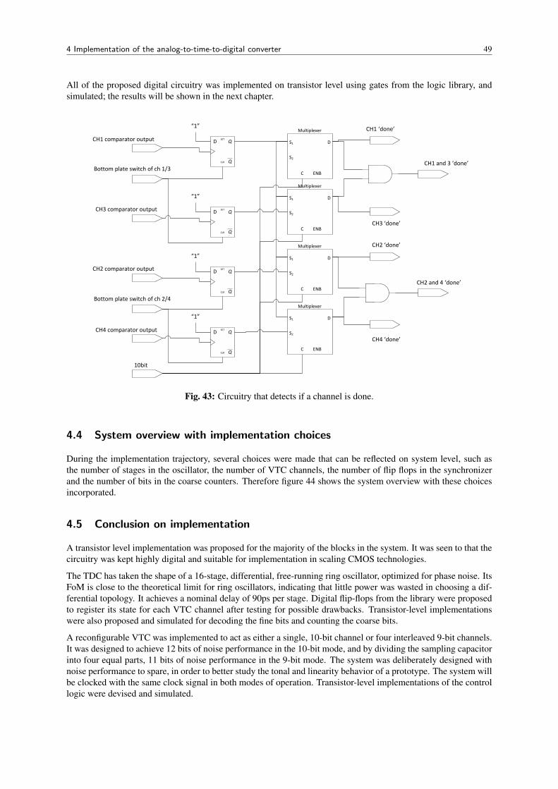
4 Implementation of the analog-to-time-to-digital converter 49
All of the proposed digital circuitry was implemented on transistor level using gates from the logic library, andsimulated; the results will be shown in the next chapter.
CH1 comparator output S1
S2
D
C ENB
Multiplexer
S1
S2
D
C ENB
Multiplexer
S1
S2
D
C ENB
Multiplexer
S1
S2
D
C ENB
Multiplexer
Q
QSET
CLR
D
“1”
Bottom plate switch of ch 1/3
Q
QSET
CLR
D
“1”
CH3 comparator output
CH2 comparator output
Q
QSET
CLR
D
“1”
Bottom plate switch of ch 2/4
Q
QSET
CLR
D
“1”
CH4 comparator output
CH1 ‘done’
CH3 ‘done’
CH2 ‘done’
CH4 ‘done’
CH1 and 3 ‘done’
CH2 and 4 ‘done’
10bit
Fig. 43: Circuitry that detects if a channel is done.
4.4 System overview with implementation choices
During the implementation trajectory, several choices were made that can be reflected on system level, such asthe number of stages in the oscillator, the number of VTC channels, the number of flip flops in the synchronizerand the number of bits in the coarse counters. Therefore figure 44 shows the system overview with these choicesincorporated.
4.5 Conclusion on implementation
A transistor level implementation was proposed for the majority of the blocks in the system. It was seen to that thecircuitry was kept highly digital and suitable for implementation in scaling CMOS technologies.
The TDC has taken the shape of a 16-stage, differential, free-running ring oscillator, optimized for phase noise. ItsFoM is close to the theoretical limit for ring oscillators, indicating that little power was wasted in choosing a dif-ferential topology. It achieves a nominal delay of 90ps per stage. Digital flip-flops from the library were proposedto register its state for each VTC channel after testing for possible drawbacks. Transistor-level implementationswere also proposed and simulated for decoding the fine bits and counting the coarse bits.
A reconfigurable VTC was implemented to act as either a single, 10-bit channel or four interleaved 9-bit channels.It was designed to achieve 12 bits of noise performance in the 10-bit mode, and by dividing the sampling capacitorinto four equal parts, 11 bits of noise performance in the 9-bit mode. The system was deliberately designed withnoise performance to spare, in order to better study the tonal and linearity behavior of a prototype. The system willbe clocked with the same clock signal in both modes of operation. Transistor-level implementations of the controllogic were devised and simulated.

4 Implementation of the analog-to-time-to-digital converter 50
Vin
Vref Stop
SampleSample
StopVTC_Ready
Coarse data
Counter
Counter
Stop
Start
FineMSB
Mux+
-
-+
Fine data16 16 4 4
8
8
8
8
8
8
8
Start
VTC channel (1x 10-bit or 4x 9-bit)
Digital backend (1 or 4)
Start
Ramp
0
Thermoto
Binary
Count_start
Count_end_1
Count_end_2
Ringosc, buers and counters (1)
Vin/Vref
Fig. 44: System overview with choices from the implementation trajectory included.
The comparator, a non-trivial part of the VTC, was not implemented within the time span of this work. However,guidelines were given towards a power-efficient implementation tailored to this specific application. A major issuestill to be conquered is flicker noise in the comparator, since it is not (fully) compensated on topology level by thereference sampling mechanism.

5 System performance 51
5 System performance
This section presents simulation results of the TDC and VTC and discusses their impact on the overall performance.It includes simulations of the combined system and concludes with some remarks on the results.
5.1 TDC
The functionality of the TDC was verified by transient simulations. The test structure included transistor levelimplementations of the oscillator, its output buffers, two counters on opposite phases and a bank of flip-flops forregistering the state of the oscillator and counters. The flip-flops were clocked at varying points in time relative tothe start of the simulation (imitating the ‘stop’ edge). The output values of the decoded fine bits and the LSBs ofthe two coarse counters were plotted for a range of arrival times of the ‘stop’ edge. The result is shown in figure45.
Relative input time (ns)
Fig. 45: Results of transient simulations of the TDC. The plot shows final values of the outputs for varying arrivaltime of the ‘stop’ signal. The signals shown are, from top to bottom: Bit 0 (LSB), 1, 2 and 3 (MSB) of the decodedoscillator state, and the LSBs of counter 1 and 2.
The apparent sawtooth shape of the signals is due to the limited amount of simulation points that are connectedusing straight lines. In reality, the final output values are digital: either high or low. The plots reveal a functionalTDC: binary counting can be distinguished throughout the fine bits and on to the counter LSBs. Also, the togglingof the counter LSBs is placed correctly in between the toggling instants of the fine MSB. This is important, sinceit allows the fine code to correctly indicate which counter should provide a stable value at any time (refer to themetastability issue in section 3.4.1). If this were not the case, the coarse counters should be connected to a differentoscillator output phase relative to the fine decoder.

5 System performance 52
Now that the functionality of the TDC is demonstrated, some key performance points can be summarized, includingsome that were already determined in the implementation chapter:
• Power consumption: On average, the oscillator consumes 857 µW, the buffers consume 160 µW (loadedby one flip flop on each phase) and the counters consume 232 µW each. The 16 flip-flops on the 16 outputphases of the oscillator consume 390 µW in total.
• Linearity: The mismatch between stages was found to be 2.7% and will translate to a cyclic error pattern of5.4% in magnitude (see section 4.1.1. The flip-flops are expected to add 3.5% of additional mismatch to thestages (section 4.1.2). Together, these small nonlinearities are not expected to dominate the linearity of theADC, nor endanger its monotonicity.
• Thermal noise: The effects of thermal noise were calculated from the phase noise performance to lie a factor35 below mismatch effects (section 4.1.1). This is theoretically sufficient for about 18 bits of dynamic range.
An interesting note is that the flip-flops and buffers consume much more power when their clock signal is low.This originates from the internal structure of the library flip-flops: these are flip-flops consisting of a master latchand a slave latch; a simplified version is shown in figure 46. When the clock signal is low, the master latch isconstantly ‘tracking’ the data signal at high speed. Lots of power can be saved here by either designing customflip-flops or by limiting the time the clock input of the flip-flops is low (e.g. by only lowering the clock when theslope approaches the zero-crossing).
Master latch Slave latch
ClockClock
Data Out
Fig. 46: Simplified schematic of the internals of a library flip-flop.

5 System performance 53
5.2 VTC
The voltage-to time converter was extensively tested. Its transient performance will be shown first, to provide afeel for the mechanisms. Next, noise simulations are presented and finally the linearity was put to the test.
5.2.1 Transient performance
Figure 47 shows some relevant signals during a transient analysis of the VTC during 10-bit operation. The signalsshow alternating sampling of the 1V reference and 500 mV input voltage for one period of the 11MHz clock,and a slope conversion during the two subsequent periods. The differential voltage across the sampling capacitorshows sufficiently fast settling to the input value, as expected from the dimensions of the sampling switches. Theeffectiveness of the assisted level shifting mechanism is also visible.
Some circuit imperfections are visible: there is a slight bump in the differential voltage after level conversion.This is due to charge injection effects and was found to be signal-independent. It will cause a slight offset in theconversion of both the input and the reference voltage, which may require further attention.
The common-mode voltage of the capacitor shows a small glitch as the diode-connected OTA is opened and thecapacitor is included in the loop. This is also attributed to charge-injection effects into the high-ohmic nodebetween the OTA gate and the current source. Some added decoupling on this node was found to suppress theglitch effectively, but further investigation is required.
Fig. 47: Results of a transient simulation of the VTC in 10-bit mode, with a 500mV input voltage and a 1Vreference voltage. From top to bottom: The 11 MHz clock signal; the differential voltage across the samplingcapacitor; the voltage on the positive and negative terminals of the sampling capacitor; the voltage on the well ofthe sampling capacitor; the ‘sample Vin’ signal; the ‘sample Vref’ signal; the comparator output signal (‘stop’).

5 System performance 54
Figure 48 shows some relevant signals of a single channel in 9-bit operation. Although the sample clock is notshown, clearly an equal amount of time is now allotted for sampling and slope conversion. The glitches at the startof the slope conversion are also clearly visible in 9-bit mode.
Fig. 48: Results of a transient simulation of a single VTC channel in 9-bit mode, with a 500mV input voltage anda 1V reference voltage. From top to bottom: The ‘Sample Vin’ and ‘Sample Vref’ signals derived from the 11MHz clock signal; the ‘start’ signal; the voltage on the positive and negative terminals of the sampling capacitor;the differential voltage across the sampling capacitor; the comparator output signal (‘stop’).
In figure 49, the differential voltages are depicted across all four sampling capacitors in 9-bit mode. The interleavedoperation is clearly visible, producing an output value and a reference value each sample clock cycle.

5 System performance 55
Fig. 49: Results of a transient simulation of all four VTC channels in 9-bit mode, with a 500mV input voltage anda 1V reference voltage. Shown are the differential voltages across the sampling capacitor for all four channels.

5 System performance 56
5.2.2 Noise performance
The VTC sampling capacitor and current source were implemented to theoretically achieve 12 bits of noise per-formance in 10-bit mode. By means of dividing the capacitance by four, 11 bits of noise performance should beobtained in 9-bit mode. However, these calculations assumed an ideal sampler, a resistive current source and idealswitches to interconnect the four sampling capacitors in 10-bit mode. This section shows the results of applyingrealistic components at these points in the VTC.
To study the impact of implementing the current source as a degenerated MOS current source and the switchesas non-ideal switches, so-called ”Time domain periodic noise analyses” were carried out using Spectre RF. Thedetails of this type of analysis can be found in appendix D. It suffices to mention here that this analysis can be usedto determine the voltage uncertainty between two nodes in a periodically operating circuit, at any time point duringthe period. This analysis accounts for noise folding or aliasing, and it can only be set up correctly if the bandwidthof the relevant noise sources is known. Details of how this analysis was set up for the problem at hand can also befound in appendix D.
Figure 50 shows the results of three time domain noise simulations. These simulations show the voltage uncertaintyacross the capacitor at various stages during the VTC operation, for a single channel (9-bit mode) converting a full-scale input voltage of 1V. The three curves were obtained using a resistive implementation of the current source, adegenerated MOS implementation of the current source with 1 nF decoupling on the bias line and a degeneratedMOS with a more realistic 3.72 pF decoupling (i.e. a 20/20 µm MOS capacitor).
Sampling
Slope
RMS
inte
grat
ed n
oise
vol
tage
(uV
)
Time (ns)
Fig. 50: Results of a time domain noise simulation of one VTC channel in 9-bit mode. Dashed line: current sourceis implemented as a poly resistor of 182kΩ. Dash-dot: current source is a degenerated PMOS implementation,with 1nF decoupling on the bias line. Line: current source is a degenerated PMOS implementation with a 20/20µmpoly capacitor (3.72 pF) on the bias line.
All three implementations show an equal voltage uncertainty during and after sampling, but a different increase

5 System performance 57
in uncertainty while integrating the noisy current source, as expected. After sampling, a voltage uncertainty of√kT/C = 86µV is expected for all three implementations. The simulations show about 74µV. This deviation
indicates that the simulation parameters were set too liberal to include all noise. This was necessary to maintainsufficient simulation speed to generate relatively detailed plots. Subsequent noise simulations were performed withgreater accuracy, as also detailed in appendix D. In general, this resulted in figures within a few percent from theexpected values. However, since these simulations are lengthy, only the two points of interest were calculated: Thenoise after sampling and the noise right before the zero-crossing of the slope.
Since the resistive implementation has approximately Vdd −VOTA = 1.33V headroom, a voltage uncertainty of√(kT/C)∗ (1+2Vin/Vcur) = 137µV is expected at the end of the ramp (refer to equation 10). The simulation
shows 126µV, again due to the fact that the simulation parameters were set too liberal.
The noise simulations on the degenerated MOS implementation of the current source in the previous chaptershowed that it was about as noisy as a resistor with half the voltage headroom. Therefore an uncertainty of√
(kT/C)∗ (1+2Vin/12Vcur) = 173µV is expected at the end of the slope. Simulations show 164µV. More realistic
decoupling of the bias line by 3.72 pF results in an additional 21µV of noise in the final value, coming from thereference branch.
In 9-bit mode with the MOS current source and realistic decoupling capacitor, the noise is 83µV after sampling,where 86µV is expected, indicating a good match between theory and simulation with the more accurate settings.The noise increases to 190µV at the end of the slope.
This type of simulation was also used to size the transmission gates that interconnect the channels in 10-bit mode.This resulted in transmission gates of (W/L)p = 8/0.16 and (W/L)n = 2/0.16. In 10-bit mode with the MOS currentsource and realistic decoupling, the noise amounts to 58µV before the slope, where 43µV was expected with idealconnections between the sampling capacitors. The noise increases to 120µV at the end of the slope.
When designing the VTC, the total noise at the end of the slope was designed to equal the quantization noise of anideal quantizer of 12 bits for the 10-bit VTC and 11 bits for the 9-bit VTC. To see where the performance standsusing non-ideal components, the comparison can be made again. The input-referred quantization noise of an idealquantizer is given by [42]:
σv =
√Vin,peak
12 ·2B (11)
with B the number of bits. Therefore, 12 bit noise performance equals 70µV of noise, 11 bit equals 141µV, 10 bitequals 282µV and so on. So all noise sources included, the VTC shows better than 11 bit noise performance in 10-bit mode and better than 10-bit noise performance in 9-bit mode. Therefore the converter will still be quantizationnoise limited, which was intended in order to better study its tonal and linearity performance. Furthermore, thereis margin for some added noise from the comparator.

5 System performance 58
5.2.3 Linearity
To determine if the VTC circuit is sufficiently linear in both modes, the input voltage was swept from 0V to 1V insteps of 20 mV and the zero-crossing instant of the comparator was logged.
Figure 51 shows the zero-crossing time as a function of the input voltage, as well as its derivative (the voltage-to-time gain for varying input voltage). The small disturbances are most probably simulation inaccuracies. A slope isvisible in the derivative of the transfer function, indicating mainly second-order harmonic distortion (HD2). Thisis expected, since the system was constructed in a single-ended fashion, and there is always some A rough, 3-pointlinearity calculation along the lines of [50] revealed a HD2 component at -68 dB and a negligible HD3 component.Comparing this to the SNR of an ideal 9-bit quantizer SNR = 6.02 ·Nbits + 1.76 = 56dB reveals that this HD2performance is acceptable for a practical ADC. There is still some room for added nonlinear capacitance to thesystem, such as parasitics and the input capacitance of a realistic comparator.
Input voltage (V)
Rela
tive
outp
ut ti
me
(ns)
Der
ivat
ive
of re
lativ
e ou
tput
tim
e (n
s/V
)
Fig. 51: Output time as a function of input voltage of the VTC in 9-bit mode (top) and its derivative for linearitycalculations (bottom).
Figure 52 shows the same plots for the system in 10-bit mode. A remarkable difference with the 9-bit mode isthat a parabola-shaped derivative is now visible, indicating a substantial amount of third-order harmonic distortion(HD3). Indeed, the same type of linearity calculation now shows an HD2 of -76dB and an HD3 of -60dB. TheSNR of an ideal 10-bit quantizer is 62 dB, so this performance is barely acceptable for a 10-bit ADC. The third-order nonlinearity is probably due to the nonlinear capacitances added by the rather large transmission gates thatinterconnect the sampling capacitances. This requires further investigation.
Both situations also show that the range for very low input voltages may be unusable. This is caused by thecomparator having to toggle almost immediately after the slope has started. The signals that have led to thedischarging of the capacitor are then mostly glitches caused by the switching of the OTA. This topic also requiresfurther attention.

5 System performance 59
Input voltage (V)
Rela
tive
outp
ut ti
me
(ns)
Der
ivat
ive
of re
lativ
e ou
tput
tim
e (n
s/V
)
Fig. 52: Output time as a function of input voltage of the VTC in 10-bit mode (top) and its derivative for linearitycalculations (bottom).

5 System performance 60
5.3 Complete system
Figure 53 shows a transient simulation of the complete system, configured in 10-bit mode, operating from the 11MHz sample clock. The reset signal for the VTC is resynchronized with the falling edge of the clock, such thatthe state machines start operating on the next rising edge. One phase of the asynchronous ring oscillator output isshown, as well as the LSBs of the two counters on opposite phases.
The analog VTC voltages demonstrate the effectiveness of the 5-flip-flop synchronizer used between the ‘VTC ready’and ‘Start’ signals: almost 10 ns is allowed for level shifting.
Sample Vref Sample Vin
Level shift
Slope conversion Done
Fig. 53: Transient simulation of the complete system in 10-bit mode. From top to bottom: the 11 MHz clocksignal; the reset signal for the VTC and its synchronized version on the falling edge of the clock; one phase ofoscillator output; the LSBs of the two anti-phase counters; several digital control signals inside the VTC; theanalog voltages inside the VTC; the ‘start’ signal (active low) and the comparator output (‘stop’ signal); the coarseand fine bit signals assuming a value at the stop signal; the power consumption of the complete system (purple),oscillator (red) and output buffers (orange).
Power consumption
Rough estimates of the power consumption can be made from the results. The overall converter draws 2.18 mW.The main contribution of the TDC in this consumption consists of the oscillator consumption (817µW), the outputbuffers (160µW), the counters (2x232µW) and the flip-flops (396µW). This leaves roughly 300µW associatedwith the VTC. Since the VTC core consumes only the two bias currents of 2x14.7µA = 52µW, the consumptionis dominated by its control and timing circuitry.
The FoM of the converter can be estimated: Since three 11MHz clock cycles are needed to produce an outputsample, and the reference sampling mechanism also requires three cycles, the effective sample rate is 1.83 MHz.

5 System performance 61
Applying the Walden FoM [51]:
FoM =P
Fs ·2B (12)
results in a FoM of 2.32 pJ/conversion-step. This is quite far from state-of-the art [52] considering it excludes thepower consumption of the comparator and the external logic required to perform the digital division. However, thepower consumption is dominated by digital circuitry, so huge improvements are expected when this topology isported to a newer technology, as detailed in section 5.4.
Besides this, the real strength of the topology lies in the interleaved operation of multiple VTC channels on onetime base. Unfortunately, time did not permit simulating the entire system in 9-bit mode, however, a performanceestimate can be made. The consumption of the VTC core increases to 79µW caused by the added current sources.The control logic is expected to draw approximately the same amount of power. The oscillator core consumptionwill remain unchanged, the power consumption of its output buffers will increase in order to drive four channelsof flip-flops. An increase of about factor two is estimated. Four banks of flip-flops will consume four times the396µW of their current configuration. The resulting power consumption of the system will be about 3.61mW.In 9-bit mode, the interleaved system will produce an output sample every clock cycle of 11 MHz. This resultsin a FoM of 640 fJ/conversion-step. Again, this is not state-of-the-art, but promising for such a highly digitalarchitecture.
5.4 Performance estimate in 65 nm CMOS
In order to estimate the performance improvement with technology, the oscillator and its output buffers were imple-mented in 65nm CMOS. Following the same approach as that of section 4.1.1, the transistors were sized based onthe internals of digital library gates. For NMOS transistors of 0.2/0.06µm and PMOS transistors of 0.28/0.06µm,the nominal oscillation frequency of the oscillator was found to be 807 MHz. The power consumption of the os-cillator was drastically reduced compared to 140nm CMOS, at 62µW from the allowed 1.2V supply. The buffersconsumed 10µW. For both the oscillator and buffers, this is more than an order of magnitude less power con-sumption per propagation delay than demonstrated in section 4.1.1 for 140 nm CMOS. Assuming this reduction isrepresentative for the reduction in the other digital blocks, this is expected to result in about an order of magnitudebetter FoM of the overall converter in 65nm CMOS, making it approach state-of-the-art performance.
5.5 Conclusion on performance
The functionality of the VTC, TDC and combined system was largely demonstrated through various simula-tions.
The TDC was verified to function correctly by transient simulations. Combined with the results from the imple-mentation chapter on its linearity, power consumption and noise properties, its overall performance is adequate forthe application.
The functionality of the VTC was also verified in both modes by transient simulations. Furthermore, time domainnoise simulations agree with the calculated values and show that the system has noise margin left for the inclusionof a non-ideal comparator. Linearity simulations indicate that the system needs some work, showing an undesiredHD3 component in 10-bit mode. This is attributed to the nonlinear capacitance added by the transmission gatesthat interconnect the channels and requires further attention. However, only about 3 dB of linearity needs to begained for acceptable performance.
Transient simulations of the complete system in 10-bit mode allowed for a rough estimation of its power consump-tion, which resulted in a figure-of-merit of 2.32 pJ/conversion-step in 10-bit mode and, by extrapolating the resultsfrom the test in 10-bit mode, 640 fJ/conversion-step in 9-bit mode. Both are quite far from state-of-the-art and stillexclude the comparator. However, most of the power is consumed by digital blocks, which shows there is room forsignificant improvement in a more modern CMOS process. Preliminary simulations indicate that in 65nm CMOS,the performance of this concept can indeed compete with state-of-the-art converters.

5 System performance 62
There are some points that require attention, such as the glitches and other charge injection effects in the VTC.Also, the power consumption of the flip-flops may be reduced significantly with relatively little effort.

6 Discussion of portability, scaleability and limitations of the concept 63
6 Discussion of portability, scaleability and limitations of the concept
Reflecting on the results so far, some qualitative remarks can be made on the scaleability, technology-portabilityand limitations of the concept.
6.1 Technology-portability
The circuit inventory shows many digital blocks, which are by definition technology-portable. The more criticalcomponents are the oscillator and the VTC.
As for the oscillator, the proposed implementation is expected to survive technology scaling, as each stage consistsof a stack of two NMOS transistors and two PMOS transistors, which is also about the minimum ‘stack’ that isrequired to implement some functional digital gates. An expected issue with scaling transistors is that the flickernoise corner in the oscillator moves upward in frequency, necessitating more frequent reference conversions. Ifthis becomes a real problem, it may be necessary to switch to a simpler inverter-based ring oscillator with an oddnumber of stages at the cost of some additional digital hardware, since in such oscillators, flicker noise can beeffectively suppressed by designing for equal rise and fall times [47].
The VTC was also designed to be compatible with newer technologies: the OTA transistor in the VTC consumeslittle more than one threshold voltage from the available supply, leaving room for a large swing across the capacitoron one side, and a large headroom to implement the current source on the other side. This allows a large inputvoltage swing, which is in turn beneficial for the requirements of the comparator and for the size of the capacitorthat is required for sufficient noise performance. A large headroom for the current increases its effective noiseresistance and therefore also reduces the required capacitor size. Nonetheless, as technology scales, the main issueto be expected from the VTC is that the sampling capacitor becomes very large due to the limited headroom forboth the input voltage swing and the current source. Also, there may be insufficient headroom to degenerate thecurrent source to increase its effective noise resistance. Another issue that can be expected in the VTC is that abootstrap circuit will become necessary for sufficient linearity of the sampler switch.
6.2 Scaleablilty
As for the scaleability of the system, the main question is how far the concept can be pushed in terms of speed andnumber of bits.
As demonstrated in section 4.1.1, the cyclic property of the mismatch and the low thermal noise of inverter-baseddelay stages theoretically allow for the calculation of many bits in the TDC. However, there is a more practicalupper limit to the number of bits, since the calculation of more bits requires more time. During such lengthyconversions, low-frequency effects in the TDC come into play, such as supply voltage drift, temperature drift andflicker noise in the oscillator. These effects can only be compensated if a reference conversion is performed atsufficiently regular intervals, which is not possible anymore when the conversions become more lengthy than thetime constant of the degrading effects.
Also, with increasing resolution, the sampling capacitance will increase by a factor four for each bit. This becomesimpractical at some point (e.g. a 13-bit version of the current implementation, including 2 bits of over-design,would require about 150 pF of sampling capacitance). Besides, while the capacitance is increased by a factor four,the TDC requires only twice the time for conversion. Discharging four times the capacitance in twice the timerequires twice the current. As a result, power consumption of the VTC increases by a factor of two for each addedbit and may quickly dominate the power consumption of the converter, especially in more modern technologieswhere the digital blocks consume little power.
In addition, for each added bit, the slope on the capacitor voltage becomes less steep. The comparator mustresolve when this slower ramp crosses zero, but still with gate-delay accuracy. This requires more gain and lessinput-referred noise voltage from the comparator and therefore more power.
Aside from noise and other unpredictable effects, the effective number of bits also limited by the linearity perfor-mance. From the results chapter, the limiting factor turned out to be the VTC already for 10-bit resolution. Thisexcludes any nonlinear capacitance that will be added to the sampling capacitor by a realistic comparator. So if

6 Discussion of portability, scaleability and limitations of the concept 64
a higher number of bits is desired, the VTC architecture needs work; for instance, it may be possible to devise adifferential architecture based on the same principles.
The lower end of the useful number of bits is determined partly by the timing overhead: in the present concept,some time is required to resynchronize the ‘VTC ready’ signal to the start of the conversion. During this time,level conversion takes place in the VTC. If, after level conversion, only a few bits need to be calculated, this timingoverhead becomes significant. For example, from 6 bits downward, the actual conversion is expected to take aboutas much time as the time required for level shifting.
Since the linearity of the converter is also more relaxed for a low number of bits, completely different designchoices can be made. For instance, a flash TDC may be preferred over a flash ring TDC and a simpler VTC archi-tecture can be used that does not require level shifting and a virtual ground node. Even VCO-based architecturesmay be the preferred choice.
6.3 Conclusion
In conclusion, the proposed topology lends itself best for implementing a highly digital ADC of moderate reso-lution: higher than that achievable with a VCO-based ADC due to its superior linearity, but limited at the upperend by the size of the sampling capacitance becoming impractical and the conversions becoming so lengthy thatthey suffer from low-frequency effects. In general, the concept is expected to be highly portable with scalingtechnology.

7 Conclusion 65
7 Conclusion
In this work, an uncommon way of analog-to-digital conversion was investigated. The conversion takes place byfirst converting the analog input signal to a time difference between two digital transitions using a voltage-to-timeconverter (VTC), and subsequently digitizing this time difference using a time-to-digital converter (TDC).
Since TDCs can be highly digital structures, key performance points of the converter, such as power consumption,speed and silicon area, are expected to improve inherently with scaling CMOS technology. Due to the digitaldesign flow, a high ease of implementation was also expected. Furthermore, a form of reconfigurability couldbe exploited that is not trivial in conventional ADCs: trading conversion time for accuracy. The assignment wasto design and implement such an analog-to-time-to-digital converter and explore these possible advantages in theprocess.
An extensive study of many TDC topologies from literature was performed, the most important conclusion being tokeep things simple if the application does not put any specific requirements on the TDC. Ring structures were foundto be especially interesting, because of their good linearity properties. However, most simple TDC topologies arefundamentally limited in power consumption because the toggling of one digital gate is required for the calculationof each quantization step.
A system architecture was proposed in which the TDC was implemented as a ‘flash ring’ TDC, more specificallyan asynchronous ring oscillator with flip-flops to record its state. To break the fundamentally limited power con-sumption of this flash TDC, it was noted that multiple VTC channels can make interleaved use of this TDC.
Possible topologies for the VTC were investigated more conceptually and superficially. To benefit from the supe-rior linearity of the ring TDC, the VTC was implemented as a start-voltage controlled single-slope converter. Areference sampling mechanism was included in order to digitally compensate for process, voltage and temperaturevariations, as well as several flicker noise sources.
The TDC and VTC were largely implemented on transistor level in 140 nm CMOS. The TDC was designed forsufficient phase noise performance and functionally tested using transient simulation. The VTC was implementedto function as either one 10-bit channel or four interleaved 9-bit channels. Its functionality and noise performancewere found to match the theory, and to be sufficient in both modes. Its linearity performance in the 10-bit moderemains a point of attention. Implementing the continuous-time comparator required within the VTC was notperformed within the time span of the thesis.
A simulation of the entire system in 10-bit mode demonstrated its functionality and allowed for a rough figure-of-merit calculation of 2.32 pJ/conversion-step, which is expected to reduce to 640 fJ/conversion-step in interleaved9-bit mode. In both cases, the power consumption is dominated by digital blocks, therefore the system is expectedto achieve much improved performance in more modern CMOS technologies. Preliminary simulations in moremodern 65nm CMOS show that state-of-the-art performance can be expected in this case.
In conclusion, the proposed converter still requires some work and will not achieve state-of-the-art performancein 140 nm CMOS, but it does demonstrate all the expected advantages, which makes it a promising concept foranalog-to-digital conversion in scaling CMOS technology.
7.1 Recommendations
• The concept has potential for state-of-the-art performance, since its performance is dominated by the powerconsumption of digital blocks. However, it will not achieve state-of-the-art performance in CMOS14. Care-ful thought should be given if it is worthwhile to carry out a tape-out in CMOS14.
• The implications of digitally dividing the converted input voltage by the converted reference voltage shouldbe investigated. If the effects are unacceptable, a revision of the VTC architecture may be in order, such thata full scale input voltage inherently maps onto a full scale TDC output.
• The oscillator was designed from a relatively arbitrary starting point of transistor sizes found in digital gates.It could be useful to investigate if this was the right choice or if larger transistors result in a more usefuldesign point in terms of speed, power and phase noise.

7 Conclusion 66
• The assisted level switching mechanism applied in the VTC requires attention from someone more experi-enced in these mechanisms. It is suspected that substrate-well parasitics will play a significant role in thefunctionality of this circuit.
• Several imperfections in the VTC, mostly caused by charge injection effects, require further attention.
• The comparator is yet to be implemented, some guidelines were given as to how it can be tailored to theapplication. Flicker noise from the comparator is expected to form a problem, since unlike other flickernoise sources, its effects will not be fully compensated by the reference sampling mechanism.
• Power-hungry components such as the comparator, but also the flip-flops, need only be enabled close to thethreshold crossing instant of the slope. It is advised to use a low-power, slightly asymmetrical differentialpair to detect whether the zero-crossing of the slope is near. The resulting signal can be used to enable thecomparator and the flip-flops only when necessary. If the consumption of the flip-flops cannot be reducedsufficiently using this technique, consider designing custom flip-flops.

7 Conclusion 67
References
[1] Robert B. Staszewski. Digital deep-submicron CMOS frequency synthesis for RF wireless applications. PhDthesis, University of Dallas, 2002.
[2] Harlan W. Lefevre and James T. Russell. Vernier chronotron. Rev Sci Instrum, 30(3):159–166, 1959.
[3] J. Christiansen. Picosecond stopwatches: The evolution of time-to-digital converters. IEEE Solid-StateCircuits Magazine, 4(3):55–59, 2012.
[4] Minjae Lee, M. E. Heidari, and A. A. Abidi. A low-noise wideband digital phase-locked loop based on acoarse–fine time-to-digital converter with subpicosecond resolution. IEEE Journal of Solid-State Circuits, 44(10):2808–2816, 2009.
[5] M. S.-W. Chen, D. Su, and S. Mehta. A calibration-free 800 mhz fractional-n digital pll with embedded tdc.IEEE Journal of Solid-State Circuits, 45(12):2819–2827, 2010.
[6] Chun-Ming Hsu, M. Z. Straayer, and M. H. Perrott. A low-noise wide-bw 3.6-ghz digital delta-sigmafractional-n frequency synthesizer with a noise-shaping time-to-digital converter and quantization noise can-cellation. IEEE Journal of Solid-State Circuits, 43(12):2776–2786, 2008.
[7] R. B. Staszewski, S. Vemulapalli, P. Vallur, J. Wallberg, and P. T. Balsara. 1.3 v 20 ps time-to-digital converterfor frequency synthesis in 90-nm cmos. IEEE Transactions on Circuits and Systems—Part II: Express Briefs,53(3):220–224, 2006.
[8] J. Borremans, K. Vengattaramane, V. Giannini, and J. Craninckx. A 86mhz-to-12ghz digital-intensive phase-modulated fractional-n pll using a 15pj/shot 5ps tdc in 40nm digital cmos. In Proc. IEEE Int. Solid-StateCircuits Conf. Digest of Technical Papers (ISSCC), pages 480–481, 2010.
[9] J. Borremans, K. Vengattaramane, V. Giannini, B. Debaillie, W. Van Thillo, and J. Craninckx. A 86 mhz–12ghz digital-intensive pll for software-defined radios, using a 6 fj/step tdc in 40 nm digital cmos. IEEE Journalof Solid-State Circuits, 45(10):2116–2129, 2010.
[10] V. Kratyuk, P. K. Hanumolu, K. Ok, Un-Ku Moon, and K. Mayaram. A digital pll with a stochastic time-to-digital converter. IEEE Transactions on Circuits and Systems—Part I: Regular Papers, 56(8):1612–1621,2009.
[11] Seon-Kyoo Lee, Young-Hun Seo, Yunjae Suh, Hong-June Park, and Jae-Yoon Sim. A 1ghz adpll with a1.25ps minimum-resolution sub-exponent tdc in 0.18um cmos. In Proc. IEEE Int. Solid-State Circuits Conf.Digest of Technical Papers (ISSCC), pages 482–483, 2010.
[12] T. Hashimoto, H. Yamazaki, A. Muramatsu, T. Sato, and A. Inoue. Time-to-digital converter with vernierdelay mismatch compensation for high resolution on-die clock jitter measurement. In Proc. IEEE Symp. VLSICircuits, pages 166–167, 2008.
[13] E. Raisanen-Ruotsalainen, T. Rahkonen, and J. Kostamovaara. An integrated time-to-digital converter with30-ps single-shot precision. IEEE Journal of Solid-State Circuits, 35(10):1507–1510, 2000.
[14] Joakim Bergs. Design of a vco based adc in a 180 nm cmos process for use in positron emission tomography.Master’s thesis, Lule University of Technology, 2010.
[15] S. Masuda, T. Watanabe, S. Yamauchi, and T. Terasawa. All-digital quadrature detection with tad for radio-controlled clocks/watches. IEEE Transactions on Circuits and Systems—Part I: Regular Papers, 56(2):285–293, 2009.
[16] T. Watanabe, S. Masuda, and H. Wakairo. An rcc receiver ic with tad-dqd and adpll using frequency multi-plying number with decimals. In Proc. Joint with the 22nd European Frequency and Time forum FrequencyControl Symp. IEEE Int, pages 478–481, 2009.
[17] T. Watanabe, S. Yamauchi, and T. Terasawa. A 0.0027-mm2 9.5-bit 50-ms/s all-digital a/d converter tad in65-nm digital cmos. In Proc. 16th IEEE Int. Conf. Electronics, Circuits, and Systems ICECS 2009, pages271–274, 2009.
7 Conclusion 68
[18] R.H.M. van Veldhoven. Analog to digital conversion circuit and method, Jun 2011.
[19] T. E. Rahkonen and J. T. Kostamovaara. The use of stabilized cmos delay lines for the digitization of shorttime intervals. IEEE Journal of Solid-State Circuits, 28(8):887–894, 1993.
[20] R. B. Staszewski, Chih-Ming Hung, K. Maggio, J. Wallberg, D. Leipold, and P. T. Balsara. All-digital phase-domain tx frequency synthesizer for bluetooth radios in 0.13μm cmos. In Proc. Digest of TechnicalPapers Solid-State Circuits Conf. ISSCC. 2004 IEEE Int, pages 272–527, 2004.
[21] P. Dudek, S. Szczepanski, and J. V. Hatfield. A high-resolution cmos time-to-digital converter utilizing avernier delay line. IEEE Journal of Solid-State Circuits, 35(2):240–247, 2000.
[22] A. K. M. K. Mollah, R. Rosales, S. Tabatabaei, J. Cicalo, and A. Ivanov. Design of a tunable differential ringoscillator with short start-up and switching transients. IEEE Transactions on Circuits and Systems—Part I:Regular Papers, 54(12):2669–2682, 2007.
[23] Jianjun Yu, F. F. Dai, and R. C. Jaeger. A 12-bit vernier ring time-to-digital converter in 0.13 um cmostechnology. IEEE Journal of Solid-State Circuits, 45(4):830–842, 2010.
[24] Poki Chen, Chun-Chi Chen, Jia-Chi Zheng, and You-Sheng Shen. A pvt insensitive vernier-based time-to-digital converter with extended input range and high accuracy. IEEE Transactions on Nuclear Science, 54(2):294–302, 2007.
[25] R. Szplet and K. Klepacki. An fpga-integrated time-to-digital converter based on two-stage pulse shrinking.IEEE Transactions on Instrumentation and Measurement, 59(6):1663–1670, 2010.
[26] Minjae Lee and A. A. Abidi. A 9 b, 1.25 ps resolution coarse–fine time-to-digital converter in 90 nm cmosthat amplifies a time residue. IEEE Journal of Solid-State Circuits, 43(4):769–777, 2008.
[27] S. Mandai, T. Iizuka, T. Nakura, M. Ikeda, and K. Asada. Time-to-digital converter based on time differenceamplifier with non-linearity calibration. In Proc. ESSCIRC, pages 266–269, 2010.
[28] Hayun Chung, H. Ishikuro, and T. Kuroda. A 10-bit 80-ms/s decision-select successive approximation tdc in65-nm cmos. IEEE Journal of Solid-State Circuits, 47(5):1232–1241, 2012.
[29] M. Z. Straayer and M. H. Perrott. A multi-path gated ring oscillator tdc with first-order noise shaping. IEEEJournal of Solid-State Circuits, 44(4):1089–1098, 2009.
[30] A. Elshazly, Sachin Rao, B. Young, and P. K. Hanumolu. A 13b 315fsrms 2mw 500ms/s 1mhz bandwidthhighly digital time-to-digital converter using switched ring oscillators. In Proc. IEEE Int. Solid-State CircuitsConf. Digest of Technical Papers (ISSCC), pages 464–466, 2012.
[31] Y. Cao, W. De Cock, M. Steyaert, and P. Leroux. 1-1-1 mash delta sigma time-to-digital converters with 6 psresolution and third-order noise-shaping. IEEE Journal of Solid-State Circuits, 47(9):2093–2106, 2012.
[32] S. Henzler, S. Koeppe, D. Lorenz, W. Kamp, R. Kuenemund, and D. Schmitt-Landsiedel. A local passivetime interpolation concept for variation-tolerant high-resolution time-to-digital conversion. IEEE Journal ofSolid-State Circuits, 43(7):1666–1676, 2008.
[33] K. Vengattaramane, J. Borremans, M. Steyaert, and J. Craninckx. A gated ring oscillator based parallel-tdcsystem with digital resolution enhancement. In Solid-State Circuits Conference, 2009. A-SSCC 2009. IEEEAsian, 2009.
[34] V. Ramakrishnan and P. T. Balsara. A wide-range, high-resolution, compact, cmos time to digital converter.In Proc. th Int VLSI Design Held jointly with 5th Int. Conf. Embedded Systems and Design. Conf, 2006.
[35] A. Mantyniemi, T. Rahkonen, and J. Kostamovaara. A cmos time-to-digital converter (tdc) based on a cyclictime domain successive approximation interpolation method. IEEE Journal of Solid-State Circuits, 44(11):3067–3078, 2009.
[36] A. S. Yousif and J. W. Haslett. A fine resolution tdc architecture for next generation pet imaging. IEEETransactions on Nuclear Science, 54(5):1574–1582, 2007.

7 Conclusion 69
[37] Wayne C. Goeke. An 8 1/2-digit integrating analog-to-digital converter with 16-bit, 100,000-sample-per-second performance. Hewlett-Packard Journal, April:8–14, 1989.
[38] Young-Gyu Yoon, Sang-Hyun Park, and SeongHwan Cho. A time-based noise shaping analog-to-digital con-verter using a gated-ring oscillator. In Proc. IEEE MTT-S Int Intelligent Radio for Future Personal Terminals(IMWS-IRFPT) Microwave Workshop Series, pages 1–4, 2011.
[39] Min Park and M. H. Perrott. A single-slope 80ms/s adc using two-step time-to-digital conversion. In Proc.IEEE Int. Symp. Circuits and Systems ISCAS 2009, pages 1125–1128, 2009.
[40] V. Dhanasekaran, M. Gambhir, M.M. Elsayed, E. Snchez-Sinencio, J. Silva-Martinez, C. Mishra, L. Chen,and E. Pankratz. A 20mhz bw 68db dr ct sigma-delta adc based on a multi- bit time-domain quantizer andfeedback element. In Proc. IEEE Int. Solid-State Circuits Conf. Digest of Technical Papers (ISSCC), 2009.
[41] Y. M. Tousi and E. Afshari. A miniature 2 mw 4 bit 1.2 gs/s delay-line-based adc in 65 nm cmos. IEEEJournal of Solid-State Circuits, 46(10):2312–2325, 2011.
[42] Bernhard E. Boser. Ee lecture 247: Analog-digital interface integrated circuits, filters - outcomes, chapter11: Sampling circuits. Online, 2011. URL http://www.eecs.berkeley.edu/~boser/courses/247/
lectures/11_sampling_circuits.pdf.
[43] David Ricketts John A. McNeill. The Designer’s Guide to Jitter in Ring Oscillators. Springer, 2009.
[44] N. Van Helleputte and G. Gielen. A 70 pj/pulse analog front-end in 130 nm cmos for uwb impulse radioreceivers. IEEE Journal of Solid-State Circuits, 44(7):1862–1871, 2009.
[45] P. Kinget. Analog Circuit Design: (X)DSL and Other Communication Systems; RF MOST Models; IntegratedFilters and Oscillators, chapter Integrated GHz voltage controlled oscillators, page 353381. Kluwer, boston,ma edition, 1999.
[46] Paul Geraedts, Ed van Tuijl, Eric Klumperink, and Bram Nauta. Towards minimum achievable phase noiseof relaxation oscillators. To be published in International Journal of Circuit Theory and Applications, 2012.
[47] A. Hajimiri, S. Limotyrakis, and T. H. Lee. Jitter and phase noise in ring oscillators. IEEE Journal ofSolid-State Circuits, 34(6):790–804, 1999.
[48] Guansheng Li, Y. M. Tousi, A. Hassibi, and E. Afshari. Delay-line-based analog-to-digital converters. IEEETransactions on Circuits and Systems—Part II: Express Briefs, 56(6):464–468, 2009.
[49] T. Sepke, P. Holloway, C. G. Sodini, and H.-S. Lee. Noise analysis for comparator-based circuits. IEEETransactions on Circuits and Systems—Part I: Regular Papers, 56(3):541–553, 2009.
[50] W. Sansen. Distortion in elementary transistor circuits. IEEE Transactions on Circuits and Systems—Part II:Analog and Digital Signal Processing, 46(3):315–325, 1999.
[51] R. H. Walden. Analog-to-digital converter survey and analysis. IEEE Journal on Selected Areas in Commu-nications, 17(4):539–550, 1999.
[52] B. Murmann. Adc performance survey 1997-2012. Online, October 2012. URL http://www.stanford.
edu/~murmann/adcsurvey.html.
[53] Xiang Gao, B. Nauta, and E. A. M. Klumperink. Advantages of shift registers over dlls for flexible low jittermultiphase clock generation. IEEE Transactions on Circuits and Systems—Part II: Express Briefs, 55(3):244–248, 2008.
[54] A. A. Abidi. Phase noise and jitter in cmos ring oscillators. IEEE Journal of Solid-State Circuits, 41(8):1803–1816, 2006.
[55] Ken Kundert. Simulating switched-capacitor filters with spectrerf. Online, July 2006. URL www.
designers-guide.org.

A List of performance metrics for ADCs and TDCs 70
A List of performance metrics for ADCs and TDCs
Since many ADC techniques have their direct counterpart in TDCs, many well-known performance metrics areapplicable on both ADC and TDC level.
Furthermore, TDCs can be tested with sinusoidal input signals just like ADCs, for instance by modulating a pulsewidth by a sinewave. This makes the performance metrics not only of theoretical, but also of practical importancefor TDCs.
The following performance metrics can be defined for reference purposes:
• Dynamic range (DR): Ratio between the power of a uniform distribution of input values and the power ofthe converter noise floor. For an ideal N-bit quantizer, DR = 6.02 ·N. For a thermal noise limited quantizer,the dynamic range is lower. Harmonic distortion products are excluded from the calculation.
• Signal-to-Noise ratio (SNR): Ratio between the power of a full-scale sinewave input and the power of theconverter noise floor. Typically 1.761 dB higher than the DR.
• Total harmonic distortion (THD): Ratio between the power of a full-scale sinewave input and the combinedpower of all harmonics.
• Signal-to-Noise-and-Distortion ratio (SINAD or SNDR): Ratio between the power of a full-scale sinewaveinput signal and the power of all other products, including noise and distortion.
• Effective number of bits (ENOB): The number of bits in an ideal quantizer that would yield the same SINADas the measured one. Calculated using ENOB = SINAD−1.761dB
6.02 .
• Figure-of-Merit (FoM): The average amount of energy required to calculate one level in time or amplitude.This work will use the Walden FoM [51], defined as FoM = P
2ENOB· fs, where P is the power consumption of
the converter and fs is the sampling frequency.
• Integral nonlinearity (INL): The deviation of the converter transfer function (time to output code) from alinear fit, expressed in LSBs.
• Differential nonlinearity (DNL): The derivative of the INL, expressed in LSBs.
• Gain error: The ratio between the average converter transfer function gain and the desired gain.
• Offset: The offset of the converter transfer function from the desired transfer function.
• Non-monotonicity: An imperfection in the converter that leads to an increasing signal generating a decreas-ing code.
• Missing code: An imperfection in the converter that leads to an output code that cannot be generated by anyinput value.
• Power consumption: The average power consumption of the converter from the supply.
• Area: The silicon area occupied by the converter.
• Resolution: The range of input values represented by one output code, although a ‘higher resolution’ impliesa smaller range represented by one code.
Besides performance metrics that can be applied to both ADCs and TDCs, there is one TDC-specific performancemeasure that is worth mentioning:
• Single-shot precision (SSP): The variance of the output code when a static time input is applied, expressedin LSBs.

B Noise and matching of inverter-based delay elements 71
B Noise and matching of inverter-based delay elements
For current-mode logic, a jitter-power FoM has been defined in [53]. This FoM demonstrates that for a CML delaystage, when all topological choices are made, both thermal and mismatch jitter are proportional to the power andthe realized delay.
For a full-swing transition through a CMOS inverter, the thermal jitter in the propagation delay td is approximatelygiven by [54]:
σ2td =
4kT γ tdI(Vdd−Vth)
(13)
where I is the saturated current of the active transistor, and γ is its noise factor. Given a load capacitance C andneglecting the crowbar current, the power consumed to realize td is
P =CV 2
dd2td
(14)
and the delay until the output crosses Vdd/2 can be written in terms of C and I:
td =CVdd
2I(15)
combining 13, 14 and 15 and normalizing the jitter by P/(1mW) to compensate for admittance scaling, yields:
σ2td,normalized =
4kT γtdVdd
(Vdd−Vth)(1mW)= td · c ·
Vdd
1mW(16)
which shows that for CMOS inverters, the thermal jitter per power is also proportional to the realized delay.

C Successive approximation TDC concept 72
C Successive approximation TDC concept
An early idea in this assignment was to create an unrolled successive-approximation (SAR) TDC. The mechanismfor a 5-bit TDC using this concept is shown in figure 54. In contrast to the main part of this thesis, the image showsa ‘bipolar’ input: the ‘input’ edge can arrive at in a time span centered around the reference edge. An arbiter orphase detector detects which edge arrives first and sets a multiplexer to send the earlier edge into a delay of 8 units.After that, the same process is repeated for 4, 2, 1 units. Buffer units are required to delay the edges while thephase detectors decide. After the decision of bit 4, the edges are aligned with an accuracy of below one gate delay.These aligned edges could be sent to for instance a VDL TDC to resolve even more bits.
The five bits can also be used to set a second path such that the reference edge will experience the delays thatit skipped until now. The result is a reference edge that should always experience the same net delay. Thisoutput reference edge could be used in for instance a locked loop to tune the delays, or in some sort of calibrationprocedure.
PD PD PDPD
48
PD
22 1
4 8221
Ref
In
Bit0 Bit1 Bit2 Bit3 Bit4
Bit0Bit1Bit2Bit3Bit4
Ref_out
To ne delay line?
Fig. 54: Illustration of an early proposal for a SAR TDC.
The idea stemmed from the following observation: When increasing the dynamic range (number of stages) of aflash TDC, the deterministic jitter due to mismatch starts impairing the linearity long before the effects of thermaljitter become visible. However, there is no way to ‘worsen’ the thermal jitter performance of the individual stageswithout slowing down the entire TDC. In a SAR TDC, the delays are lumped into 1, 2, 4, 8, ... 256, 512 ... andthese larger delays may offer more possibilities to trade power for noise performance.
This is reinforced by the observations from appendix B. It is shown that several types of delay elements have afixed jitter-power figure of merit. In other words, to implement a certain amount of delay with a certain amount ofjitter, a fixed amount of power is required. So if there is jitter to spare, power can be gained. Large delays such as256 unit delays can now be implemented for instance as 128 current-starved delays drawing half the power.
There is a number of practical reasons why this SAR TDC concept was not carried out further. The main reason isthe issue of metastability: the last arbiters have to resolve time differences in the order of a few LSBs every clock

C Successive approximation TDC concept 73
cycle. Therefore their metastability behavior is crucial: if the arbiters cannot decide within the buffer delay time,the multiplexer is not set in time, and the sample is lost for the next stages. A thorough metastability study andarbiter design did not fit within the time span of this thesis.
Furthermore, there are indications that mismatch-jitter will scale with the same quantities as thermal jitter, soeffectively nothing may be gained by current-starving the long delays [53], but this was not verified for specificdelay implementations, such as current-starved inverters, within this thesis.

D Spectre RF time domain noise analysis 74
D Spectre RF time domain noise analysis
Spectre RF time domain noise analysis [55] uses the periodic steady state (PSS) of a periodically operating circuitto determine the voltage uncertainty between any two nodes at any point during the fundamental period. Naturally,it requires the periodic steady state (PSS) of the circuit to be known.
The analysis will be executed for each time point of interest during the period, and for each noise frequency at thattime point. It starts from an instant somewhere in the periodic steady state and cycles through the PSS to find theaccumulated noise at that frequency. It accounts for folding (aliasing) of noise in sampled circuits into the bandfrom 0 to half the fundamental frequency.
Knowing the bandwidth of the relevant noise sources is the key to correct simulation results. An example willfollow, but suppose the system has a fundamental frequency (e.g. the clock frequency) of ffund. Suppose the noisesource of interest band-limited to a frequency fnoise = N · ffund. To find reasonable initial results, the followingprocedure may be followed in setting up the analysis.
First of all, the PSS needs include sufficient harmonics, to say anything about what happens at higher frequencies(that will fold back into the signal band of a sampled system). Therefore, the number of harmonics must be set toabove N. Secondly, the PSS needs to be sufficiently accurate to include these high frequencies. Therefore, in theoptions of the PSS settings, the parameter ‘maxac’ must be set to above fnoise.
Next, a ‘pnoise’ analysis must be enabled, with the noise ranging from the lowest value of interest (e.g. 1 Hz) tohalf the fundamental frequency ffund, in for instance 10 steps per decade. Higher frequencies do not need to beincluded, even if fnoise is much higher, since the pnoise analysis will automatically account for noise folding. Also,the parameter ‘maxsideband’ must be set to above N, but slightly smaller than the number of harmonics includedin the PSS simulation. Finally, the number of time points must be specified at which the integrated noise should becalculated (e.g. 20 points during a full period). Specific instants can also be listed, such as the time just before orafter a switch opens or closes in a sampled system.
D.1 Applying the analysis to the VTC
The aforementioned procedure was applied to the VTC in section 5.2.2. This section lists the specifics of thatanalysis.
The noise sources with the highest bandwidth in this circuit are the sampling switches. Their resistance at a 1Vinput is approximately 1.35kΩ, which, together with the sampling capacitance of 556fF implies a noise bandwidthof 212MHz. Another relevant noise source is the current source, however, it has a lower bandwith, since its highoutput impedance forms a low-pass filter with the sampling capacitance. Also, the bias line of the current sourceis decoupled to the supply rail to limit the noise bandwidth.
The test circuit for noise testing purposes is actuated by a clock signal of 5MHz; this is the PSS fundamental fre-quency. Since the noise extends to 212MHz or 42 times the fundamental, at least 42 harmonics of the fundamentalneed to be included in the PSS simulation.
To generate the relatively detailed plots of figure 50, loose simulation parameters were chosen: 50 harmonics, 48sidebands and ‘maxac’ = 240 MHz.
Since the plots showed a deviation of approximately 14% below the expected values, more conservative simulationsettings were used for subsequent simulations that required only two time points. For these simulations, 100harmonics, ‘maxac’ = 500 MHz and 95 sidebands were used. Deviations were now only a few percents below theexpected values.

E MATLAB code 75
E MATLAB code
E.1 Process flip-flop Monte-Carlo simulations
1 % Calculates offset of flipflops based on montecarlo simulations for2 % different input voltages3
4 % Probability that flipflop samples the voltage as positive5 Pv = [0.01 0.06 0.16 0.34 0.57 0.75 0.91 0.98 1];6 % corresponding input voltages7 V = [0.83:0.01:0.91];8 Ntrials = 100;9
10 % Probability that flipflop samples edge as positive11 Pt = [0 0.01 0.03 0.07 0.13 0.18 0.28 0.35 ...12 0.45 0.59 0.66 0.82 0.9 0.95 0.98 0.99 1];13 % Corresponding input times14 T = [337:1:353].*1e−12;15
16 % Choose the input to be used in the remainder of the script17 Xin = T;18 Yin = Pt;19
20 % Create matrix with column of successes and column of trials21 Y = [Yin'*Ntrials repmat(Ntrials,size(Yin'))];22
23 % Fit binomial distribution, store result24 b = glmfit(Xin,Y,'binomial','link','probit');25
26 % Pick some points at which to evaluate the fitted curve27 refx = linspace(min(Xin),max(Xin),50);28
29 yfit = glmval(b,refx,'probit');30 figure31 hold on32
33 % Plot the sampled distribution34 plot(Xin,Yin,'ob');35 % Plot the fitted distribution36 th = plot(refx,yfit,'−−r');37 % Plot the corresponding normal distribution38 mu = −b(1)/b(2)39 sigma = 1/b(2)40
41 %line(refx,normcdf(refx,mu,sigma),'color','g');42
43 box on44 hold off45
46 legend('Mismatch simulations','binomial distribution fit','Location','East');47 xlabel('Clock delay (sec)');48 ylabel('Probability of positive output');49 title('INL of delay line vs delay ring');
E.2 Calculate INL profiles of a ring and linear TDC
1 delay = 90.7e−12; % Nominal delay of elements2 sigma rel = 0.027; % Relative stddev of delay elements3 sigma thermal rel = 0.00077; % Random deviation of elements (thermal noise)4 ringstages = 18; % Number of stages in the ring implementation5 bits = 18; % Number of bits to be calculated6 numplots = 1; % Number of randomizations to plot7
8 % Calculate absolute sigma9 sigma = delay*sigma rel;

E MATLAB code 76
10 sigma thermal = delay*sigma thermal rel;11
12 % Calculate the number of "laps" the signal can go round in the ring13 laps = ceil(2ˆbits/ringstages);14
15 hold off;16 plot(1:1:laps*ringstages,delay*ones(1,laps*ringstages),'k−−', ...17 1:1:laps*ringstages,−delay*ones(1,laps*ringstages),'k−−');18 ylim([−2*delay 2*delay]);19 xlim([1 laps*ringstages]);20 hold on;21
22 for I = 1:numplots23 % Straight line is accumulation of independent delays24 Nomline = (1:1:laps*ringstages).*delay;25 Sigmaline = cumsum(sigma*randn(1,laps*ringstages)+sigma thermal*randn(1,laps*ringstages));26 Qline = Nomline + Sigmaline;27
28 % Ring is accumulation of repeated delays29 Nomring = (1:1:laps*ringstages).*delay;30 Sigmaring = cumsum(repmat(sigma*randn(1,ringstages),1,laps) ...31 + sigma thermal*randn(1,laps*ringstages));32 Qring = Nomring + Sigmaring;33
34 % Calculate fit for slope and offset correction35 A = polyfit(1:1:laps*ringstages,Sigmaring,1);36 B = polyfit(1:1:laps*ringstages,Sigmaline,1);37
38 plot(1:1:laps*ringstages,Sigmaring−A(1)*(1:1:laps*ringstages)−A(2),'b−', ...39 1:1:laps*ringstages,Sigmaline−B(1)*(1:1:laps*ringstages)−B(2),'r−');40 end41
42 xlabel('Code');43 ylabel('INL (sec)');44 title('INL of delay line vs delay ring');