Design and Implementation of an Adaptive Delta Sigma...
44
Design & Implementation of an Adaptive Delta Sigma Modulator Shahrukh Athar MS CmpE 07 2007-06-0008 Project Supervisor: Dr Shahid Masud
Transcript of Design and Implementation of an Adaptive Delta Sigma...

Design & Implementation
of an Adaptive Delta
Sigma Modulator
Shahrukh Athar
MS CmpE 07
2007-06-0008
Project Supervisor: Dr Shahid Masud
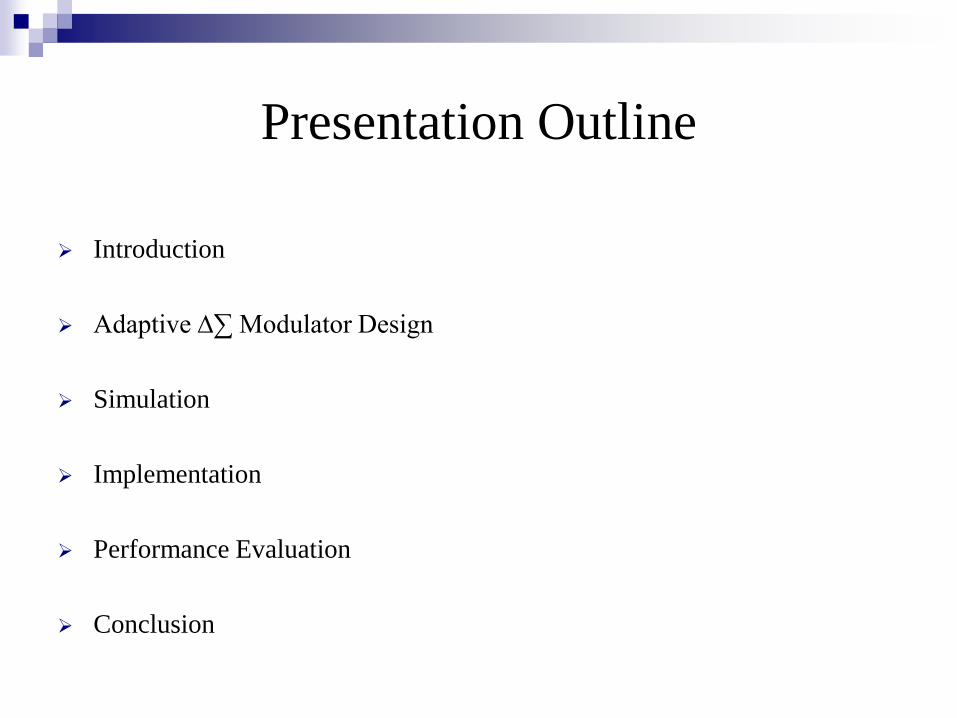
Presentation Outline
Introduction
Adaptive ∆∑ Modulator Design
Simulation
Implementation
Performance Evaluation
Conclusion

Introduction
Delta Sigma modulators are used in the design of:
Analog to Digital converters (ADC)
Digital to Analog converters (DAC)
Frequency Synthesizers
Digital Radios
Oscillators
They use the techniques of:
Oversampling
Noise Shaping
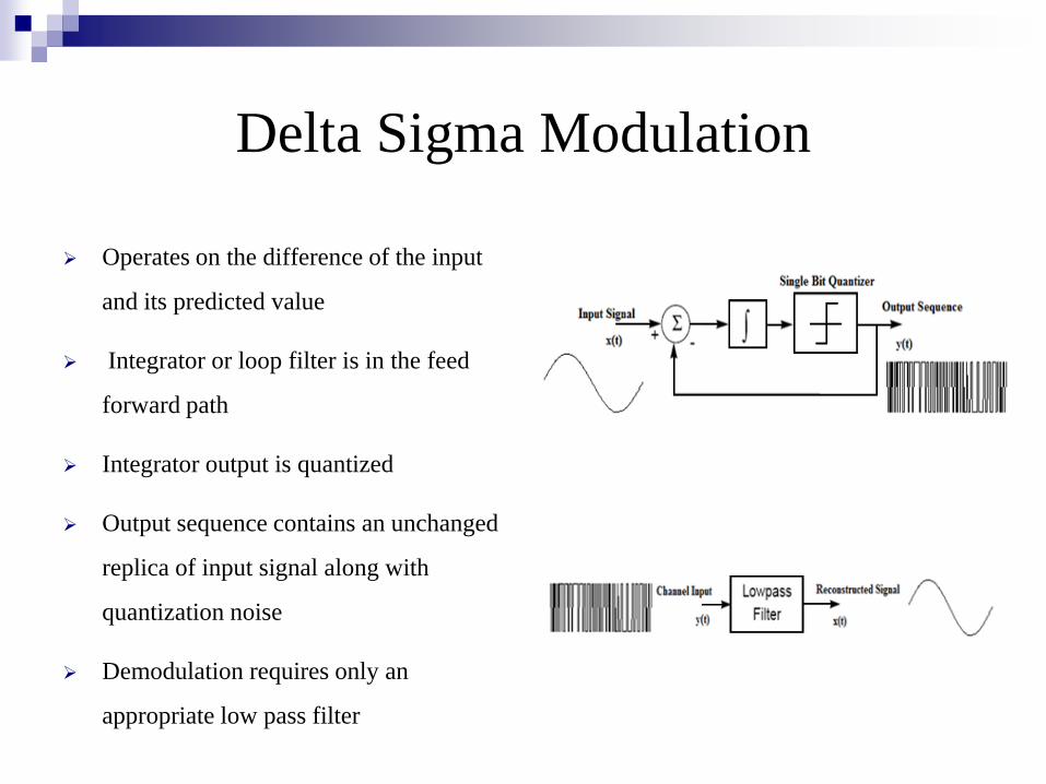
Delta Sigma Modulation
Operates on the difference of the input
and its predicted value
Integrator or loop filter is in the feed
forward path
Integrator output is quantized
Output sequence contains an unchanged
replica of input signal along with
quantization noise
Demodulation requires only an
appropriate low pass filter

Advantages of
Oversampling and Noise Shaping
Oversampling spreads the
quantization noise and reduces
the noise floor
Noise Shaping removes
quantization noise from the band
of interest by pushing it out
∆∑ modulation incorporates
oversampling and noise shaping
Higher Order ∆∑ Modulators
High order modulators use loop filter of higher order
Advantages
Perform better noise shaping and remove more quantization noise from the band of
interest
When in stable operation they have a better SQNR and resolution
Disadvantages
Signal dependent quantizer gain which degrades noise shaping for large input
magnitudes
Performance is not uniform for time varying inputs
Less stable
More complex and consume more power
Multi-bit Quantizer based
∆∑ Modulators
Multi-bit quantizer can be used instead of the single bit quantizer
Advantages
Can handle larger input swings
Reduce quantization noise and hence increase SQNR and resolution
Disadvantages
Require multi-bit DACs in the modulator feedback loop which introduce non linear
characteristics
Require more area on chip and consume more power

Advantages of
1st Order Single Bit ∆∑ Modulator
Simple and robust
Easy to implement
Power efficient
Signal independent quantizer gain
Stable for varying inputs
Single bit quantizer does not require multi-bit DAC
Almost linear behavior
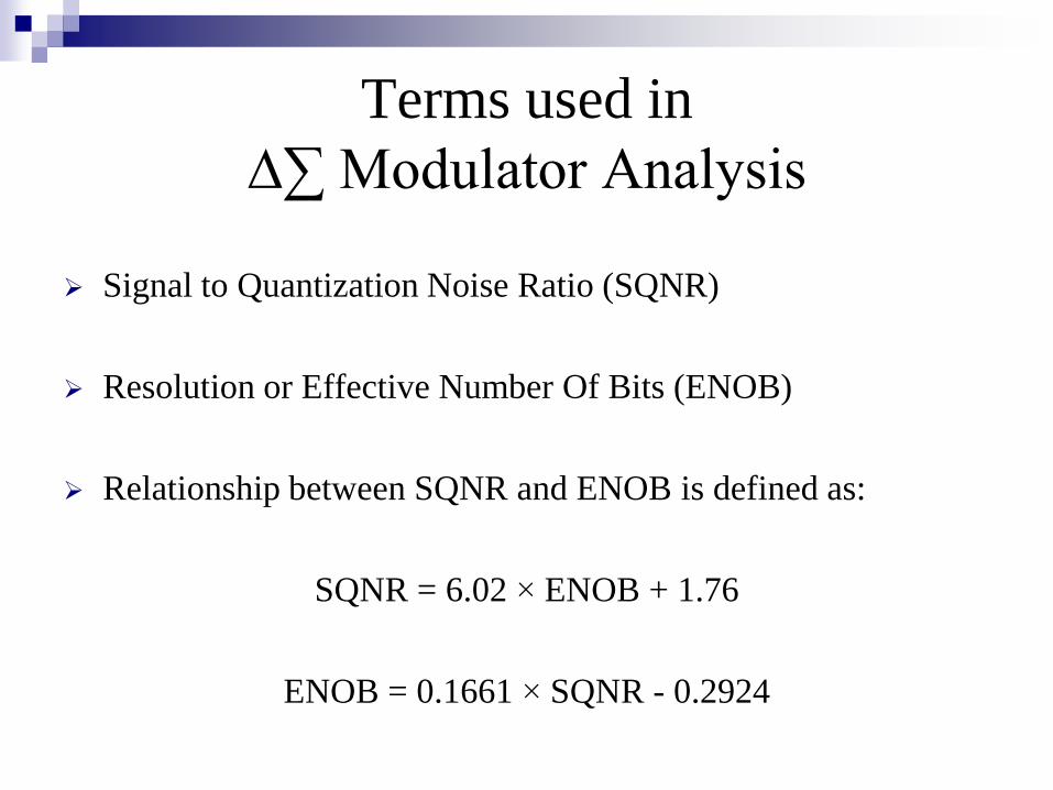
Terms used in
∆∑ Modulator Analysis
Signal to Quantization Noise Ratio (SQNR)
Resolution or Effective Number Of Bits (ENOB)
Relationship between SQNR and ENOB is defined as:
SQNR = 6.02 × ENOB + 1.76
ENOB = 0.1661 × SQNR - 0.2924

Adaptive ∆∑ Modulator
It should adapt the amplitude of the ∆∑ output signal to the amplitude of the input signal
Based on variations in input signal power/magnitude
This project is based on the adaptive ∆∑ modulator design and adaptation algorithm reported by Zierhofer,
C. M., in [13] and [14].
Input power can be estimated by
Forward Estimation
Backward Estimation
Types of adaptation algorithms
Syllabic Adaptation
Instantaneous Adaptation
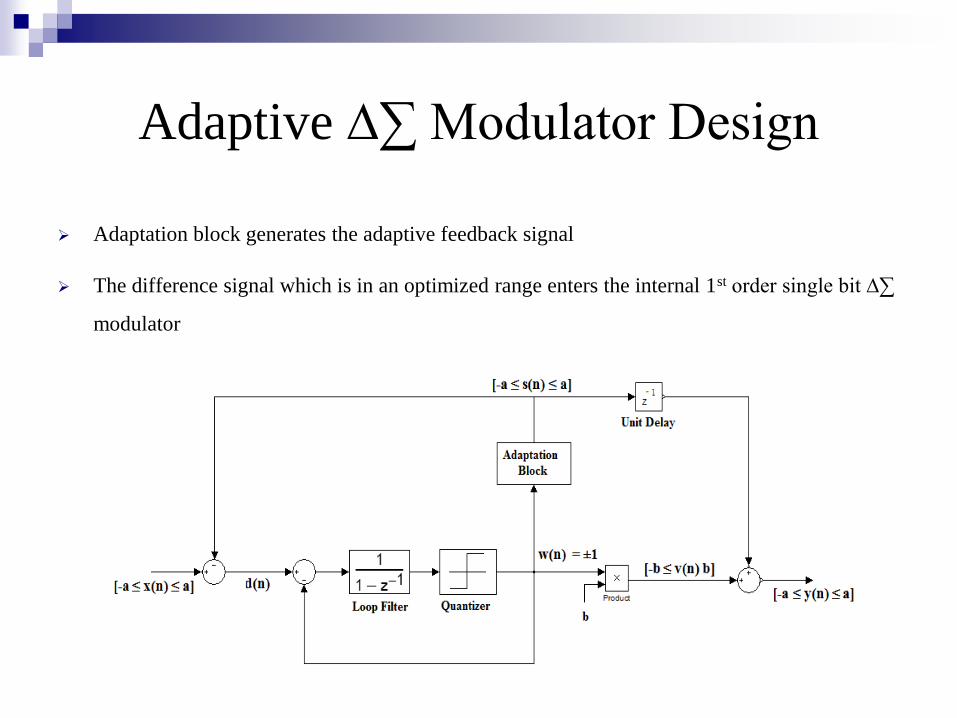
Adaptive ∆∑ Modulator Design
Adaptation block generates the adaptive feedback signal
The difference signal which is in an optimized range enters the internal 1st order single bit ∆∑
modulator

Adaptation Algorithm
The adaptive feedback signal should be a rough estimate of the input signal
A continuous string of +1s or -1s appear at the output if tracking is lost
Adaptation stage measures the local density of +1s and -1s
Changes adaptive feedback signal if a threshold is crossed
Adaptation Algorithm based on Instantaneous Adaptation
Sample Values Adaptive Feedback
Signal s(n)w(n) w(n-1) w(n-2)
+1 +1 +1 s(n)=s(n-1)+bq
-1 -1 -1 s(n)=s(n-1)-bq
All other combinations s(n)=s(n-1)

Advantages of
Adaptive ∆∑ Modulation
Uses a 1st order single bit ∆∑ modulator which is stable and simple to implement
Can handle input signals of larger swing
Reduces quantization noise because
Output is tracking the Input
Input to the internal ∆∑ modulator is in an optimized range
Power consumption is
Comparable to 1st order single bit ∆∑ modulator
Much less than higher order ∆∑ modulators
Output sequence is multi-level and performance is
Comparable to multi-bit quantizer based ∆∑ modulators
Uses only a Single Bit Quantizer

Simulation of the
Adaptive ∆∑ Modulator
Simulation tools used:
MATLAB version 7.7.0.471 (R2008b)
Simulink version 7.2 (R2008b)
Modulator types simulated:
Non-Adaptive 1st Order Single Bit ∆∑ Modulator
Adaptive ∆∑ Modulator
Input to and Output from the modulators is sent to MATLAB workspace
for evaluation of SQNR
Types of Input Signals Used
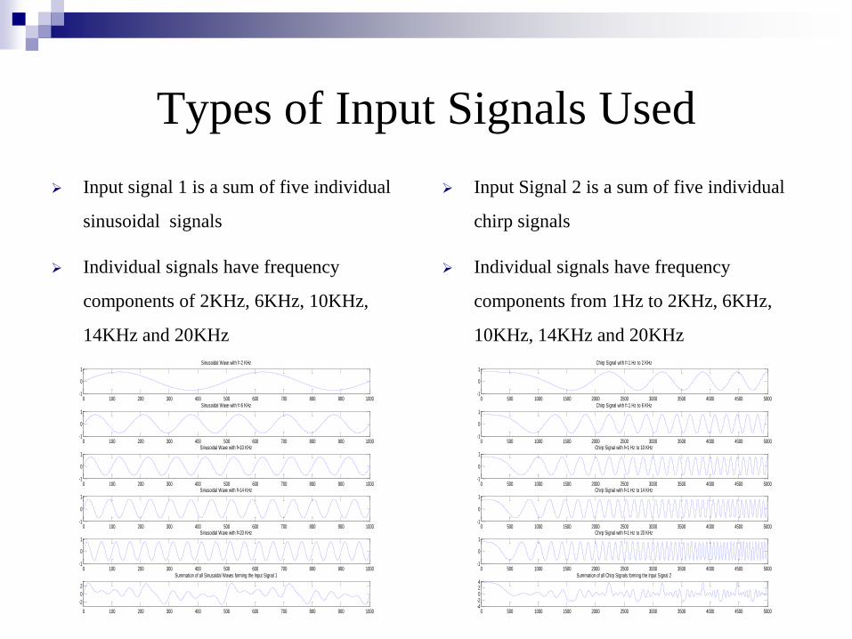
Input signal 1 is a sum of five individual
sinusoidal signals
Individual signals have frequency
components of 2KHz, 6KHz, 10KHz,
14KHz and 20KHz
Input Signal 2 is a sum of five individual
chirp signals
Individual signals have frequency
components from 1Hz to 2KHz, 6KHz,
10KHz, 14KHz and 20KHz
0 100 200 300 400 500 600 700 800 900 1000-1
0
1Sinusoidal Wave with f=2 KHz
0 100 200 300 400 500 600 700 800 900 1000-1
0
1Sinusoidal Wave with f=6 KHz
0 100 200 300 400 500 600 700 800 900 1000-1
0
1Sinusoidal Wave with f=10 KHz
0 100 200 300 400 500 600 700 800 900 1000-1
0
1Sinusoidal Wave with f=14 KHz
0 100 200 300 400 500 600 700 800 900 1000-1
0
1Sinusoidal Wave with f=20 KHz
0 100 200 300 400 500 600 700 800 900 1000
-2
0
2
Summation of all Sinusoidal Waves forming the Input Signal 1
0 500 1000 1500 2000 2500 3000 3500 4000 4500 5000-1
0
1Chirp Signal with f=1 Hz to 2 KHz
0 500 1000 1500 2000 2500 3000 3500 4000 4500 5000-1
0
1Chirp Signal with f=1 Hz to 6 KHz
0 500 1000 1500 2000 2500 3000 3500 4000 4500 5000-1
0
1Chirp Signal with f=1 Hz to 10 KHz
0 500 1000 1500 2000 2500 3000 3500 4000 4500 5000-1
0
1Chirp Signal with f=1 Hz to 14 KHz
0 500 1000 1500 2000 2500 3000 3500 4000 4500 5000-1
0
1Chirp Signal with f=1 Hz to 20 KHz
0 500 1000 1500 2000 2500 3000 3500 4000 4500 5000-4-2024
Summation of all Chirp Signals forming the Input Signal 2
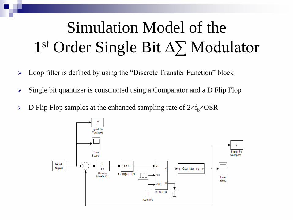
Simulation Model of the
1st Order Single Bit ∆∑ Modulator
Loop filter is defined by using the “Discrete Transfer Function” block
Single bit quantizer is constructed using a Comparator and a D Flip Flop
D Flip Flop samples at the enhanced sampling rate of 2×fb×OSR

Simulation Model of the
Adaptive ∆∑ Modulator
All components of the adaptive ∆∑ modulator except the adaptation stage are shown here
1st order single bit ∆∑ modulator used as the internal modulator

Simulation Model of the
Adaptive ∆∑ Modulator
The adaptation stage checks for five consecutive +1s or -1s [14] and is shown here
It is constructed by using simple components such as delays, relational operators, switches and adders
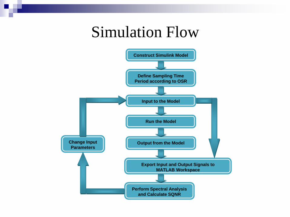
Simulation Flow
Construct Simulink Model
Define Sampling Time
Period according to OSR
Input to the Model
Run the Model
Output from the Model
Export Input and Output Signals to
MATLAB Workspace
Perform Spectral Analysis
and Calculate SQNR
Change Input
Parameters

Implementation of the
Adaptive ∆∑ Modulator
The implementation tools used are:
Xilinx System Generator for DSP v10.1
ChipScope Pro Analyzer v10.1
These tools requires prior installation of the following:
Xilinx Integrated Software Environment (ISE) v10.1
MATLAB version 7.4.0.287 (R2007a)
Simulink version 6.6 (R2007a)
Modulator types Emulated and Implemented:
Non-Adaptive 1st Order Single Bit ∆∑ Modulator
Adaptive ∆∑ Modulator
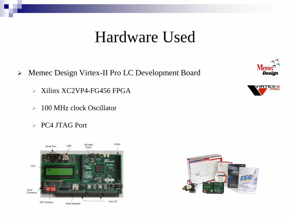
Hardware Used
Memec Design Virtex-II Pro LC Development Board
Xilinx XC2VP4-FG456 FPGA
100 MHz clock Oscillator
PC4 JTAG Port
Xilinx System Generator for DSP
Integrates itself with Simulink
Ability to connect to Simulink blocks
Ability to generate Verilog HDL code from models
Supports Register Transfer Level implementation
Supports Xilinx IP Core implementation
Supports hardware Co-Simulation
Supports hardware Emulation
Supports Design Bitstream Generation
Enables working with ChipScope Pro Analyzer

Implementation Model of the
1st Order Single Bit ∆∑ Modulator
1st order loop filter is implemented as an accumulator
Single bit quantizer is implemented using a relational operator and multiplexer
Simulink system period set according to the OSR
Gateway In coverts the input from Simulink double to fixed point format
Gateway Out converts output to Simulink double and gives it back

Implementation Model of the
Adaptive ∆∑ Modulator
All components of the adaptive ∆∑ modulator except the adaptation stage are shown here
1st order single bit ∆∑ modulator used as the internal modulator
Simulink system period set according to the OSR

Implementation Model of the
Adaptive ∆∑ Modulator
The adaptation stage checks for three consecutive +1s or -1s [13] and is shown here
It is constructed by using simple components such as delays, relational operators, multiplexers and adders

Time Domain Emulation ResultsNon Adaptive ∆∑ Modulator
0 100 200 300 400 500 600 700 800 900 1000
-1
0
1
Input Signal to the first order single bit Delta Sigma Modulator
0 100 200 300 400 500 600 700 800 900 1000
-1
0
1
Output Signal from the first order single bit Delta Sigma Modulator

Time Domain Emulation ResultsAdaptive ∆∑ Modulator
0 100 200 300 400 500 600 700 800 900 1000-2
0
2Input Signal x(n)
0 100 200 300 400 500 600 700 800 900 1000-2
0
2Adaptive Feedback Signal S(n)
0 100 200 300 400 500 600 700 800 900 1000-2
0
2Difference Signal d(n)
0 100 200 300 400 500 600 700 800 900 1000-2
0
2First Order Delta Sigma Sequence w(n)
0 100 200 300 400 500 600 700 800 900 1000-2
0
2v(n)=b*w(n)
0 100 200 300 400 500 600 700 800 900 1000-2
0
2Final Adaptive Delta Sigma Sequence
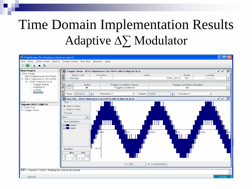
Time Domain Implementation ResultsAdaptive ∆∑ Modulator

Emulation FlowConstruct Xilinx Model
Define Simulink System
Period according to OSR
Simulink Input to the Model
Run the Xilinx Model
Output from the Model
obtained in Simulink
Export Input and Output Signals to
MATLAB Workspace
Perform Spectral Analysis
and Calculate SQNR
Change Simulink
Input Parameters

Implementation Flow
Define the System Generator Parameters
Generate Bitstream File
Detect FPGA in ChipScope Pro Analyzer
Download the Bitstream file to the FPGA
Set Trigger condition & Run the Project
Actual FPGA Output visible on ChipScope Pro Analyzer
Export actual Input and Output Signals from ChipScope Pro Analyzer to MATLAB Workspace
Perform Spectral Analysis & calculate SQNR
Construct the Xilinx System Generator for DSP Model
Performance Evaluation
Spectral Analysis for Input Signals of
Low Power
Moderate Power
High Power
Spectral Analysis on data received from the FPGA
Input Power versus Output SQNR
Input Power versus Resolution
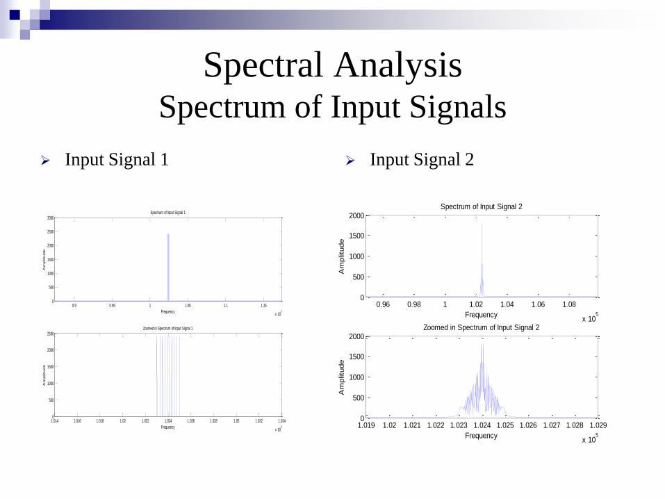
Spectral AnalysisSpectrum of Input Signals
Input Signal 1 Input Signal 2
0.9 0.95 1 1.05 1.1 1.15
x 105
0
500
1000
1500
2000
2500
3000
Frequency
Am
plitude
Spectrum of Input Signal 1
1.014 1.016 1.018 1.02 1.022 1.024 1.026 1.028 1.03 1.032 1.034
x 105
0
500
1000
1500
2000
2500
Frequency
Am
plitude
Zoomed in Spectrum of Input Signal 1
0.96 0.98 1 1.02 1.04 1.06 1.08
x 105
0
500
1000
1500
2000
Frequency
Am
plitu
de
Spectrum of Input Signal 2
1.019 1.02 1.021 1.022 1.023 1.024 1.025 1.026 1.027 1.028 1.029
x 105
0
500
1000
1500
2000
Frequency
Am
plitu
de
Zoomed in Spectrum of Input Signal 2

Spectral AnalysisLow Power Input Signals
Non-Adaptive ∆∑ Modulator Adaptive ∆∑ Modulator
0 1 2 3 4 5 6 7 8 9 10
x 104
0
50
Am
plitu
de
Spectrum of Input Signal
4 4.5 5 5.5 6 6.5
x 104
0
50
Am
plitu
de
Spectrum of the Delta Sigma Output Signal
4.95 5 5.05 5.1 5.15 5.2 5.25 5.3
x 104
0
50
Frequency
Am
plitu
de
Zoomed in Spectrum of the Delta Sigma Output Signal
0 1 2 3 4 5 6 7 8 9 10
x 104
0
50
Am
plitu
de
Spectrum of Input Signal
4 4.5 5 5.5 6 6.5
x 104
0
50
Am
plitu
de
Spectrum of the Delta Sigma Output Signal
4.95 5 5.05 5.1 5.15 5.2 5.25 5.3
x 104
0
50
Frequency
Am
plitu
de
Zoomed in Spectrum of the Delta Sigma Output Signal

Spectral AnalysisModerate Power Input Signals
Non-Adaptive ∆∑ Modulator Adaptive ∆∑ Modulator
3 4 5 6 7 8
x 104
0
500
1000
1500
Frequency
Am
plitu
de
Spectrum of the Delta Sigma Output Signal
4.7 4.8 4.9 5 5.1 5.2 5.3 5.4 5.5 5.6
x 104
0
500
1000
1500
Frequency
Am
plitu
de
Zoomed in Spectrum of the Delta Sigma Output Signal
3 4 5 6 7 8
x 104
0
500
1000
1500
Frequency
Am
plitu
de
Spectrum of the Delta Sigma Output Signal
4.7 4.8 4.9 5 5.1 5.2 5.3 5.4 5.5 5.6
x 104
0
500
1000
1500
Frequency
Am
plitu
de
Zoomed in Spectrum of the Delta Sigma Output Signal

Spectral AnalysisHigh Power Input Signals
Non-Adaptive ∆∑ Modulator Adaptive ∆∑ Modulator
0.7 0.8 0.9 1 1.1 1.2 1.3 1.4
x 105
0
0.5
1
1.5
2x 10
4
Frequency
Am
plit
ude
Spectrum of the Delta Sigma Output Signal
0.9 0.95 1 1.05 1.1 1.15
x 105
0
1000
2000
3000
4000
5000
Frequency
Am
plit
ude
Zoomed in Spectrum of the Delta Sigma Output Signal
0.7 0.8 0.9 1 1.1 1.2 1.3 1.4
x 105
0
0.5
1
1.5
2x 10
4
Frequency
Am
plit
ude
Spectrum of the Delta Sigma Output Signal
0.9 0.95 1 1.05 1.1 1.15
x 105
0
1000
2000
3000
4000
5000
Frequency
Am
plit
ude
Zoomed in Spectrum of the Delta Sigma Output Signal
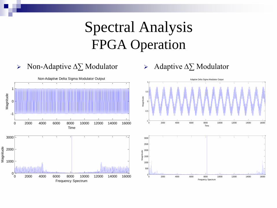
Spectral AnalysisFPGA Operation
Non-Adaptive ∆∑ Modulator Adaptive ∆∑ Modulator
0 2000 4000 6000 8000 10000 12000 14000 16000
-1
0
1
Time
Magnitude
Non-Adaptive Delta Sigma Modulator Output
0 2000 4000 6000 8000 10000 12000 14000 160000
1000
2000
3000
Frequency Spectrum
Magnitude
0 2000 4000 6000 8000 10000 12000 14000 16000-1
-0.5
0
0.5
1
Time
Magnitude
Adaptive Delta Sigma Modulator Output
0 2000 4000 6000 8000 10000 12000 14000 160000
500
1000
1500
2000
2500
3000
Frequency Spectrum
Magnitude
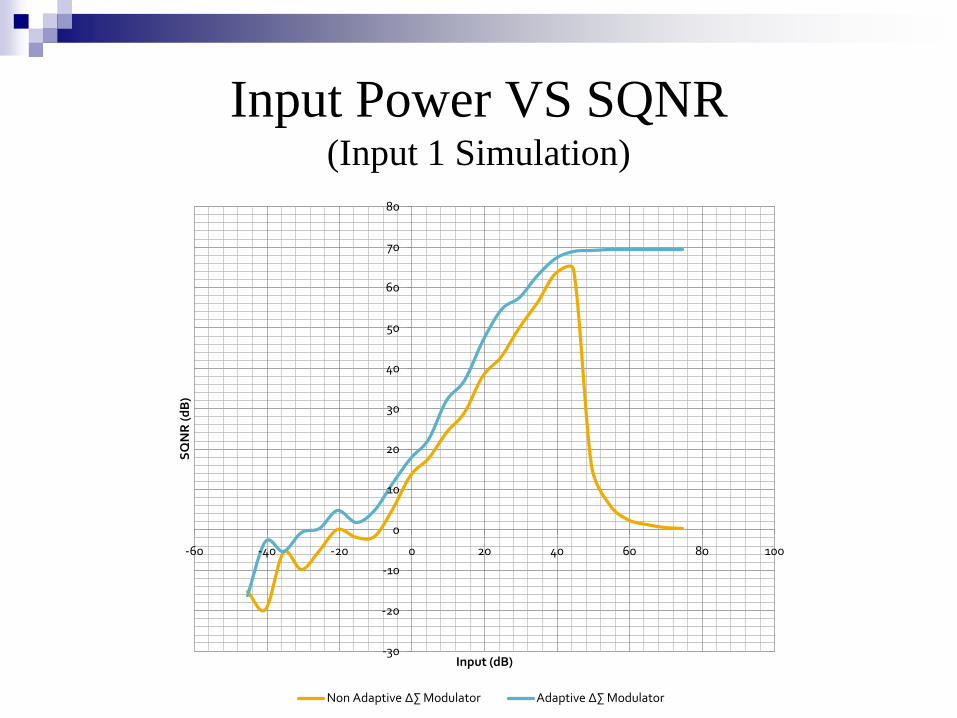
Input Power VS SQNR(Input 1 Simulation)
-30
-20
-10
0
10
20
30
40
50
60
70
80
-60 -40 -20 0 20 40 60 80 100
SQ
NR
(d
B)
Input (dB)
Non Adaptive ∆∑ Modulator Adaptive ∆∑ Modulator

Input Power VS SQNR(Input 2 Emulation)
-30
-20
-10
0
10
20
30
40
-60 -40 -20 0 20 40 60
SQ
NR
(d
B)
Input (dB)
Non Adaptive ∆∑ Modulator Adaptive ∆∑ Modulator
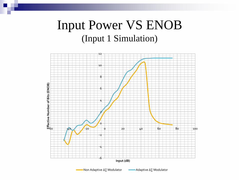
Input Power VS ENOB(Input 1 Simulation)
-6
-4
-2
0
2
4
6
8
10
12
-60 -40 -20 0 20 40 60 80 100Eff
ect
ive
Nu
mb
er
of
Bit
s (E
NO
B)
Input (dB)
Non Adaptive ∆∑ Modulator Adaptive ∆∑ Modulator

Input Power VS ENOB(Input 2 Emulation)
-5
-4
-3
-2
-1
0
1
2
3
4
5
6
-60 -40 -20 0 20 40 60
Eff
ect
ive
Nu
mb
er
of
Bit
s (E
NO
B)
Input Power (dB)
Non Adaptive ∆∑ Modulator Adaptive ∆∑ Modulator
Conclusion
An adaptive ∆∑ modulator was successfully simulated and implemented
Its notable characteristics are:
Stability and simplicity of a 1st order single bit ∆∑ modulator
Performance comparable to
2nd order ∆∑ modulators
Multi-bit Quantizer based ∆∑ modulators
Ability to handle larger input swings
Ability to handle signals with low and high power better than the corresponding non-adaptive
∆∑ modulator
Better SQNR and Resolution when compared to the corresponding non-adaptive
∆∑ modulator
References
1. Bourdopoulos, G. I., et al., Eds., Delta-Sigma Modulators: Modeling, Design and Applications, Imperial College Press, 2003.
2. Schreier, R. & Temes, G., Eds., Understanding Delta-Sigma data Converters, a John Wiley & Sons Inc., publication, 2005.
3. Park, S., Motorola Digital signal Processors: Principles of Sigma-Delta Modulation for Analog-to-Digital Converters, Strategic
Applications, digital Signal Processor Operation (http://www.numerix-dsp.com/appsnotes/APR8-sigma-delta.pdf).
4. Wang, H., Brennan, P. & Jiang, D., FPGA Implementation of Sigma-Delta Modulators in Fractional-N Frequency Synthesis,
International Symposium on Signals, Circuits and Systems, Volume 1, Page(s): 1-4, 13-14 July 2007.
5. Ramesh, M. C. & Chao, K.S., Sigma Delta Analog to Digital Converters with Adaptive Quantization, Proceedings of the 40th
Midwest Symposium on Circuits and Systems, vol. 1, Pages(s): 22-25, 3-6 August 1997.
6. Morgado, A., Rio, R. D. & Roan, J. M., An Adaptive Sigma Delta Modulator for Multi-Standard Hand-held Wireless Devices, IEEE
Asian Solid-State Circuits Conference, November 12-14, 2007.
7. Benabes, P. & Guessab, S., A Sigma-Delta Converter with Adjustable Tradeoff between Resolution and Consumption, 14th IEEE
International Conference on Electronics, Circuits and Systems, Page(s): 230-233, 11-14 Dec 2007.
8. Chakravarthy, C. V., An amplitude-controlled adaptive delta sigma modulator, The Radio and Electronic Engineer, vol 49, no. 1,
Page(s): 49-54, 1979.
9. Yu, J., Sandler, M. B. & Hawken, R. E., Adaptive quantization for one-bit sigma-delta modulation, IEE Proceedings G: Circuits,
Devices and Systems, vol. 139, no. 1, Page(s): 39-44, 1992.
References
10. Dunn, C. & Sandler, M., Fixed and adaptive sigma-delta modulator with multibit quantizers, Applied Signal Processing, vol. 3, no.
4, Page(s): 212-222, 1996.
11. Jaggi, M. P. & Chakravarthy, C. V., Instantaneously adaptive delta sigma modulator, Canadian Electrical Engineering Journal, vol.
11, no. 1, Page(s): 3-6, 1986.
12. Aldajani, M. A. & Sayed, A. H., Stability and performance of an adaptive sigma-delta modulator, IEEE Transactions on Circuits
and Systems II, vol. 48, Page(s): 233-244, 2001.
13. Zierhofer, C. M., Adaptive Delta-Sigma Modulation with one-bit Quantization, United States Patent Application Publication; Pub.
No.: US 2003/0146865 A1; Pub. Date: Aug 7, 2003.
14. Zierhofer, C.M., Adaptive Delta-Sigma Modulation for Enhanced Input Dynamic Range, EURASIP Journal on Advances in Signal
Processing, Volume 2008 (2008), Article ID 439203, 7 pages. Austria. Accepted 1 June 2008.
15. Shehata, K. A., et al., An FPGA Based 1-Bit All Digital Transmitter employing Delta-Sigma Modulation with RF Output for SDR,
International Conference on Signals, Circuits and Systems, 2008.
16. System Generator for DSP v10.1 user guide. (http://www.xilinx.com/support/sw_manuals/sysgen_user.pdf).
17. Xilinx System Generator for DSP v10.1 help.
18. Xilinx Virtex-II Pro LC Development Board user’s guide. (http://www.ux.uis.no/~karlsk/MIK200/dok/2VPxLC-UG.pdf)