Design and Implementation of a Wearable Device for ...
163
University of Calgary PRISM: University of Calgary's Digital Repository Graduate Studies The Vault: Electronic Theses and Dissertations 2016 Design and Implementation of a Wearable Device for Prosopagnosia Rehabilitation Lu, Kok Yee Lu, K. Y. (2016). Design and Implementation of a Wearable Device for Prosopagnosia Rehabilitation (Unpublished master's thesis). University of Calgary, Calgary, AB. doi:10.11575/PRISM/25570 http://hdl.handle.net/11023/3219 master thesis University of Calgary graduate students retain copyright ownership and moral rights for their thesis. You may use this material in any way that is permitted by the Copyright Act or through licensing that has been assigned to the document. For uses that are not allowable under copyright legislation or licensing, you are required to seek permission. Downloaded from PRISM: https://prism.ucalgary.ca
Transcript of Design and Implementation of a Wearable Device for ...
University of Calgary
PRISM: University of Calgary's Digital Repository
Graduate Studies The Vault: Electronic Theses and Dissertations
2016
Design and Implementation of a Wearable Device for
Prosopagnosia Rehabilitation
Lu, Kok Yee
Lu, K. Y. (2016). Design and Implementation of a Wearable Device for Prosopagnosia
Rehabilitation (Unpublished master's thesis). University of Calgary, Calgary, AB.
doi:10.11575/PRISM/25570
http://hdl.handle.net/11023/3219
master thesis
University of Calgary graduate students retain copyright ownership and moral rights for their
thesis. You may use this material in any way that is permitted by the Copyright Act or through
licensing that has been assigned to the document. For uses that are not allowable under
copyright legislation or licensing, you are required to seek permission.
Downloaded from PRISM: https://prism.ucalgary.ca

UNIVERSITY OF CALGARY
Design and Implementation of a Wearable Device for Prosopagnosia Rehabilitation
by
Kok Yee Lu
A THESIS
SUBMITTED TO THE FACULTY OF GRADUATE STUDIES
IN PARTIAL FULFILMENT OF THE REQUIREMENTS FOR THE
DEGREE OF MASTER OF SCIENCE
GRADUATE PROGRAM IN ELECTRICAL ENGINEERING
CALGARY, ALBERTA
AUGUST, 2016
© Kok Yee Lu 2016

P a g e |
ii
Abstract
This study introduces a wearable facial recognition system for face blindness, or
prosopagnosia, rehabilitation. Prosopagnosia is the inability to recognize familiar faces, which
affects 2.5% of the world population (148 million people). The design and implementation of a
facial recognition system tailored to patients with prosopagnosia is a priority in the field of clinical
neuroscience. The goal of this study is to demonstrate the feasibility of implementing a wearable
stand-alone (not connected to a PC or a smartphone) system-on-chip (SoC) that performs facial
recognition and could be used to assist individuals affected by prosopagnosia.
This system is designed as an autonomous embedded platform built on eyewear with SoC
and a custom designed circuit board. The implementation is based on the open source computer
vision image processing algorithms embedded within a compact-scale processor. The advantages
of the device are its lightness, compactness, single independent image processing capability and
long operational time. The system performs real-time facial recognition and informs the user of
the results by displaying the name of the recognized person.

P a g e |
iii

P a g e |
iv
Acknowledgement
First, I would like to express my sincere gratitude to my advisor, Professor Dr. Svetlana
Yanushkevich for her continuous support for my MSc study and related research, as well as for
her patience, motivation, and immense knowledge. Her guidance has helped me throughout the
research and writing of this thesis. I could not have imagined having a better advisor and mentor
for my MSc study. Additionally, I would like to thank the rest of my thesis committee: Dr. Ed
Nowicki and Dr. Steve Liang, and most importantly, Professor Giuseppe Iaria for suggesting this
research topic in the very practical area of application. We acknowledge the Canadian
Microelectronics Corporation (CMC) for providing the universities in Canada with a license for
PCB design.

P a g e |
v

P a g e |
vi
Table of Content
Abstract ......................................................................................................................................................... ii
Acknowledgement ....................................................................................................................................... iv
Table of Content .......................................................................................................................................... vi
List of Figures .............................................................................................................................................. xii
List of Tables ............................................................................................................................................... xvi
List of Symbols, Abbreviations and Nomenclature ................................................................................... xviii
Chapter 1. Introduction ................................................................................................................................ 1
1.1 Motivation for the research ................................................................................................................ 1
1.2 Study objectives and hypothesis ......................................................................................................... 2
1.3 Design approach ................................................................................................................................. 3
1.4 Research contributions ....................................................................................................................... 4
1.5 Outline of the thesis ............................................................................................................................ 6
Chapter 2. Literature Review ........................................................................................................................ 7
2.1 Introduction ........................................................................................................................................ 7
2.2 Prosopagnosia and facial recognition ................................................................................................. 7
2.3 Computerized face detection ............................................................................................................. 8
2.3.1 Facial detection using Haar Feature-Based Cascade Classifier .................................................... 8
2.3.2 Face detection using Local Binary Pattern ................................................................................. 10
2.4 Computerized facial recognition ....................................................................................................... 11
2.5 Approaches to wearable facial recognition ...................................................................................... 16
2.6 Conclusion ......................................................................................................................................... 18
Chapter 3. Wearable Device Architecture .................................................................................................. 19
3.1 Introduction ...................................................................................................................................... 19
3.2 The proposed wearable device architecture .................................................................................... 19

P a g e |
vii
3.3 Embedded Software for face detection and recognition ................................................................. 21
3.3.1 Embedded facial recognition software ...................................................................................... 22
3.3.2 Hardware design ........................................................................................................................ 23
3.3.3 Initial wearable display prototype design .................................................................................. 24
3.3.4 Proof-of-concept for portability ................................................................................................. 26
3.4 Custom printed circuit board (PCB) design ....................................................................................... 29
3.5 Schematics design ............................................................................................................................. 32
3.5.1 DDR2 connector ......................................................................................................................... 32
3.5.2 Camera module interface .......................................................................................................... 34
3.5.3 HDMI connection ....................................................................................................................... 35
3.5.4 I/O voltage selection connector ................................................................................................. 37
3.5.5 USB interface.............................................................................................................................. 38
3.5.6 Video display .............................................................................................................................. 41
3.5.7 Power section and power management .................................................................................... 41
3.6 Conclusion ......................................................................................................................................... 44
Chapter 4. Power Section Design and Simulation ...................................................................................... 45
4.1 Introduction ...................................................................................................................................... 45
4.2 Redesigning the power section ......................................................................................................... 45
4.3 Efficiency of PAM2306 DC/DC converter on CMIO ........................................................................... 46
4.3.1 Power efficiency for 3.3V output ............................................................................................... 46
4.3.2 Power efficiency for 1.8V output ............................................................................................... 47
4.3.3 Power efficiency for 2.5V LDO output ....................................................................................... 48
4.4 Output ripple of the original PAM2306 DC/DC converter ................................................................ 49
4.4.1 Output ripple for 3.3V ................................................................................................................ 50
4.4.2 Output ripple for 2.5V ................................................................................................................ 50

P a g e |
viii
4.4.3 Output ripple for 1.8V ................................................................................................................ 52
4.5 Design of a new power section using LTC3521 ................................................................................. 53
4.5.1 Power circuit design ................................................................................................................... 54
4.5.2 Output voltage configuration .................................................................................................... 55
4.5.3 Power section and output capacitors of the DC/DC converter ................................................. 56
4.5.4 Maximum outputs current (2.5V output ripple and filtering) ................................................... 58
4.5.5 Cutoff voltage consideration for battery application ................................................................ 58
4.5.6 Inductor selection ...................................................................................................................... 59
4.6 LTspice simulation ............................................................................................................................. 60
4.6.1 Crude power sequencing simulation ......................................................................................... 61
4.6.2 Proper power sequencing .......................................................................................................... 62
4.6.3 Transient load simulation and testing of the LTC3521 DC/DC converter 2.5V output .............. 64
4.6.4 Fast Fourier Transform analysis of the LTC3521 DC/DC converter outputs .............................. 67
4.6.5 Output of the 2.5V LTC3521 DC/DC converter simulation circuit ............................................. 68
4.6.6 Output overshoot simulation for the 2.5V output ..................................................................... 69
4.6.7 Power efficiency simulation ....................................................................................................... 70
4.6.8 3.3V output voltage ................................................................................................................... 72
4.7 Schematics capture and PCB layout .................................................................................................. 73
4.7.1 Schematics capture .................................................................................................................... 74
4.7.2 PCB layout .................................................................................................................................. 75
4.8 DC/DC circuit test .............................................................................................................................. 76
4.8.1 Linear Tech LTC3521 DC/DC converter efficiency measurements ............................................ 76
4.8.2 Efficiency study of 3.3V output .................................................................................................. 77
4.8.3 Efficiency study of 2.5V output .................................................................................................. 78
4.8.4 Efficiency study of 1.8V output .................................................................................................. 79

P a g e |
ix
4.8.5 LTC3521 load tests with noise spectrum measurement ............................................................ 80
4.8.6 Load tests for 3.3V output ......................................................................................................... 81
4.8.7 Load tests for 2.5V output ......................................................................................................... 83
4.8.8 Load tests for 1.8V output ......................................................................................................... 84
4.9 Conclusion ......................................................................................................................................... 85
Chapter 5. Design of Software and Hardware for the Wearable Prototype............................................... 87
5.1 Introduction ...................................................................................................................................... 87
5.2 Wearable device prototype design overview ................................................................................... 87
5.2.1 Camera-to-processor interface connectivity ............................................................................. 87
5.2.2 Firmware level greyscale conversion for speed optimization ................................................... 88
5.2.3 HDMI to composite video converter elimination ...................................................................... 89
5.2.4 Power control box elimination .................................................................................................. 90
5.3 Facial Recognition Core Software and GUI ....................................................................................... 91
5.3.1 Graphical User Interface ............................................................................................................ 92
5.3.2 OpenCV library for facial recognition......................................................................................... 94
Face Collection Mode...................................................................................................................... 97
Training Mode ................................................................................................................................. 97
Recognition Mode ........................................................................................................................... 97
Delete All Mode .............................................................................................................................. 98
Load Mode ...................................................................................................................................... 98
Save Mode ...................................................................................................................................... 98
5.4 Wearable prototype display hardware ........................................................................................... 101
5.4.1 Display drive IC and color display selection ............................................................................. 101
5.4.2 Ultralow-power NTSC/PAL/SECAM video decoder .................................................................. 104
5.4.3 Initial display prototype ........................................................................................................... 104

P a g e |
x
5.4.4 Mechanical/industrial design prototype .................................................................................. 107
5.5 Transient voltage suppressions and over voltage protection ......................................................... 107
5.5.1 TVS or Transorb Protection ...................................................................................................... 108
5.6 Privacy requirements ...................................................................................................................... 108
5.7 Conclusion ................................................................................................................................... 110
Chapter 6. Testing the Prototype .............................................................................................................. 111
6.1 Introduction .................................................................................................................................... 111
6.2 Device power consumption during facial recognition mode .......................................................... 111
6.2.1 Raspberry Pi power consumption ............................................................................................ 111
6.2.2 Battery discharge testing ......................................................................................................... 113
6.3 Face detection and recognition accuracy ....................................................................................... 114
6.3.1 Face detection testing .............................................................................................................. 114
6.3.2 Eye detection and face detection and recognition .................................................................. 116
6.3.3 Testing the platform performance on a photo database ........................................................ 117
6.4 Power consumption and thermal characteristics ........................................................................... 117
6.5 System latency ................................................................................................................................ 118
6.6 Conclusion ....................................................................................................................................... 120
Chapter 7. Summary and Future Work ..................................................................................................... 123
7.1 Summary ......................................................................................................................................... 123
7.2 Future Work .................................................................................................................................... 125
7.2.1 ARM processors and solutions ................................................................................................. 125
Raspberry Pi 3 Compute Module (pre-release) ............................................................................ 126
Allwinner A31 Quad Core Cortex-A7 ARM Processor ................................................................... 126
Variscite DART-MX6 Quad Core Cortex-A9 ARM Processor ......................................................... 127
7.2.2 Overhead display ..................................................................................................................... 127

P a g e |
xi
7.2.3 User inputs ............................................................................................................................... 128
7.2.4 Power section design and battery operation considerations .................................................. 129
7.2.5 Further testing ......................................................................................................................... 130
7.2.6 Software Improvement ............................................................................................................ 131
References ................................................................................................................................................ 133
Appendixes ................................................................................................................................................ 137
Appendix A - Raspbian Slim-Down ........................................................................................................ 137
Appendix B - OpenCV Native Compilation ............................................................................................ 138
Appendix C - OpenCV Installation ......................................................................................................... 139
Install OpenCV ................................................................................................................................... 139
Force Display back to HDMI .............................................................................................................. 140
Appendix D - Adafruit PiTFT - 2.8" Touchscreen Display for Raspberry Pi ........................................... 141
Screen Upside-Down Adjustment ..................................................................................................... 141
Appendix E - RaspiCam ......................................................................................................................... 142
P a g e |
xii
List of Figures
Figure 1. Assembled custom PCBs designed for facial recognition (middle and right) ................................ 4
Figure 2. High-level block diagram of the facial recognition device ............................................................. 5
Figure 3. Human face features (a) and face pattern form (b) combining features from (a) ...................... 10
Figure 4. Example of an LBP operator ......................................................................................................... 11
Figure 5. Example of a set of training faces [15] ......................................................................................... 12
Figure 6. Facial recognition in operation [36] ............................................................................................. 12
Figure 7. Original face (left) and average face (right) ................................................................................. 14
Figure 8. Eigenvectors of the dataset ......................................................................................................... 14
Figure 9. Training set eigenvectors (a) and LBP (b) from the training set example [15] ............................ 16
Figure 10. Face transformation using Fisherface algorithm ....................................................................... 16
Figure 11. Compute module development kit, showing the CM and CMIO board [22] ............................. 20
Figure 12. Hardware-software organization and interface between subsystems [26] .............................. 22
Figure 13. A working prototype performing facial detection ..................................................................... 23
Figure 14. Camera interface board elimination [26] .................................................................................. 24
Figure 15. Overhead display prototyping ................................................................................................... 25
Figure 16. Sketch of the proposed wearable on-eye display ...................................................................... 25
Figure 17. System block diagram with CM and surrounding peripheral interfaces [26] ............................ 26
Figure 18. Simple setup to initial codes testing .......................................................................................... 27
Figure 19. Raspberry Pi Camera module (left) and Spy Camera module (right and bottom) [27] ............. 28
Figure 20. Raspberry Pi Camera module in enclosure (right) and Spy Camera Module (left) .................... 28
Figure 21. Raspberry Pi Compute Module Development Kit (left) and our Custom PCB (right) ................ 29
Figure 22. Completed version 2.0 of the board assembled in a 3D printed enclosure .............................. 29
Figure 23. PCB layout for the custom board showing the top layer (a) and bottom layer (b) ................... 30
Figure 24. Custom board PCB layout top side with copper poured shown in red...................................... 31

P a g e |
xiii
Figure 25. DDR2 connector ......................................................................................................................... 33
Figure 26. Raspberry Pi camera connection to the Raspberry Pi I/O board [26]........................................ 34
Figure 27. Raspberry Pi camera interface connector and signal ................................................................ 35
Figure 28. Current limit load switch (left) and HDMI connection (right) .................................................... 36
Figure 29. Revision 2 of our facial recognition processing module ............................................................ 37
Figure 30. I/O voltage selection circuit ....................................................................................................... 38
Figure 31. USB host and slave connection .................................................................................................. 39
Figure 32. USB host and slave selection for training imaging loading and boot from PC .......................... 40
Figure 33. 1.5” composite video display module (left) and with enclosure (right) [29] ............................. 41
Figure 34. Power section............................................................................................................................. 42
Figure 35. 3D printed belt-wearable power bank enclosure (blue) and installed power bank .................. 43
Figure 36. 3.6V output efficiency peak at 89 % .......................................................................................... 47
Figure 37. 1.8V output efficiency peak at 79.5% ........................................................................................ 47
Figure 38. 2.5V LDO output efficiency peak at 66%.................................................................................... 49
Figure 39. 3.3V output ripple and switching frequency ............................................................................. 50
Figure 40. Conceptual linear regulator and filter capacitors theoretically reject switching regulator ripple
and spikes ............................................................................................................................................ 51
Figure 41. 2.5V output ripple is 6.45mV peak-to-peak ............................................................................... 52
Figure 42. 1.8V output ripple 7.65mV peak-to-peak at a frequency of 1.7MHz ........................................ 53
Figure 43. LTC3521 reference circuit and the efficiency curve [31] ........................................................... 55
Figure 44. Output voltage adjustment for a buck-boost converter (a) and buck converters (b) [31] ........ 55
Figure 45. Output capacitors frequency response [32] .............................................................................. 57
Figure 46. Lithium-polymer battery discharge curve with 3.0V cutoff voltage [33]................................... 59
Figure 47. Schematics of the initial LTspice simulation model ................................................................... 60
Figure 48. LTspice simulation model of the triple outputs DC/DC controller ............................................. 61

P a g e |
xiv
Figure 49. LTC3521 DC/DC converter (left) and sequencing circuit U2 to U4 (right) using LTspice
simulation ........................................................................................................................................... 62
Figure 50. Power sequencing using LTspice simulation .............................................................................. 64
Figure 51. 2.5V circuit under test (left) and load transient circuit model (right) ....................................... 65
Figure 52. Line transient jig via commutating supplies capable of clean high-slew rate and drive12 ......... 66
Figure 53. Load transient test with 1V steps (blue), with 2.5V voltage remaining steady, using LTspice
simulation ........................................................................................................................................... 66
Figure 54. Close-up of the load transient capture using LTspice simulation .............................................. 67
Figure 55. FFT analysis of the DC/DC converter outputs ............................................................................ 68
Figure 56. 2.5V output ripple and noise for LTC3521 DC/DC converter using LTspice simulation ............. 69
Figure 57. Overshoot at startup at high efficiency using LTspice simulation ............................................. 70
Figure 58. Frequency analysis of the LT3521 outputs using LTspice simulation ........................................ 73
Figure 59. Schematics for the LTC3521 DC/DC converter .......................................................................... 74
Figure 60. 3D models of the board (a) and PCB layout (b) ......................................................................... 75
Figure 61. LT3521 efficiency measurement setup block diagram .............................................................. 77
Figure 62. Populated DC/DC switcher PCB under test ................................................................................ 77
Figure 63. Efficiency graph for 3.3V output using the LTC3521 DC/DC converter ..................................... 78
Figure 64. Efficiency graph for 2.5V output using the LTC3521 DC/DC converter ..................................... 79
Figure 65. Efficiency graph for 1.8V output using the LTC3521 DC/DC converter ..................................... 80
Figure 66. Setup for measuring power supply noise spectrum [34] ........................................................... 81
Figure 67. Frequency spectrum analysis of 3.3V output with no load ....................................................... 82
Figure 68. Frequency spectrum analysis of 3.3V output under full load condition (1000mA) ................... 82
Figure 69. Frequency spectrum analysis for 2.5V output with no load ...................................................... 83
Figure 70. Frequency spectrum analysis for 2.5V output under full load condition (600mA) ................... 83
Figure 71. Frequency spectrum analysis for 1.8V output with no load ...................................................... 84
Figure 72. Frequency spectrum analysis for 1.8V output under full load condition (600mA) ................... 84

P a g e |
xv
Figure 73. Existing design ............................................................................................................................ 86
Figure 74. New design ................................................................................................................................. 86
Figure 75. First proof-of-concept block diagram ........................................................................................ 90
Figure 76. Diagram without HDMI-to-CVBS (composite video) connection ............................................... 90
Figure 77. Power control box elimination................................................................................................... 91
Figure 78. Facial recognition software GUI ................................................................................................. 93
Figure 79. Software Initialize Phase with face and eye classifiers loading ................................................. 94
Figure 80. Detailed Logic Flow of the Facial Recognition at Software Start-up Stage ................................ 96
Figure 81. Mode Selection Flow Chart ........................................................................................................ 99
Figure 82. PreprocessedFace() Function Implementation Block Diagram ................................................ 100
Figure 83. Display circuit block diagram ................................................................................................... 101
Figure 84. Kopin display drive IC internal features and architecture ....................................................... 102
Figure 85. Pixel array layout and display module block diagram ............................................................. 103
Figure 86. Initial prototype system connection and components ............................................................ 105
Figure 87. Non-critical board elimination ................................................................................................. 106
Figure 88. Signal splicing to bypass boards ............................................................................................... 106
Figure 89. Facial recognition module inside the 3D printed enclosure (a), with the on-eye display
attached to eyeglasses (b) ................................................................................................................ 107
Figure 90. Power usage comparisons ....................................................................................................... 112
Figure 91. Lithium polymer cell phone battery discharge curve under real device load ......................... 114
Figure 92. Depiction of Edward T. Hall's ‘interpersonal distances of man’, showing radius in feet and
meters ............................................................................................................................................... 116
Figure 93. Thermal imaging camera reading of the system-on-chip IC .................................................... 118
Figure 94. Facial recognition code profiling .............................................................................................. 119
Figure 95. CC/CV charge at 4.2V, 1C, +25ºC and CC discharge at 1C to 3.0V, +25ºC ............................... 130

P a g e |
xvi
List of Tables
Table 1. Four main facial recognition steps and definitions ......................................................................... 8
Table 2. Recommended capacitance for buck DC/DC converter [31] ........................................................ 57
Table 3. DC/DC controllers maximum current output tested data ............................................................ 58
Table 4. Power dissipation on electronics components using LTspice simulation ..................................... 71
Table 5. Efficiency report using LTspice simulation .................................................................................... 71
Table 6. Output signals characteristics using LTspice simulation ............................................................... 72
Table 7. Critical components for the wearable display ............................................................................ 102
Table 8. Raspberry Pi power consumption data during facial recognition ............................................... 112
Table 9. Face detection rates in different lightning conditions ................................................................ 115
Table 10. Face detection rates by distance and face position .................................................................. 115
Table 11. Facial recognition Rate Test after 60 seconds of training ......................................................... 117
Table 12. Application removal command and descriptions ..................................................................... 137

P a g e |
xvii

P a g e |
xviii
List of Symbols, Abbreviations and Nomenclature
Abbreviations or
Nomenclatures
Definition
3D enclosure Physical enclosure printed by a 3D printer
Adafruits Spy Camera module A small-sized Raspberry Pi Camera Module
ADC Analog-to-Digital Converter
A/V Audio Video
BBB Beaglebone Black – an ARM Base SBM
BCM2835 ARM-based system-on-chip
BNC Bayonet Neill–Concelman connector
BOM Electronics components Bill-of-Materials
Boost-Buck Converter
A type of DC-to-DC converter where its output voltage can
be either greater than or less that the input voltage
CM Raspberry Pi Compute Module
CMCDA Compute Module Camera/Display Adapter Board
CSI-2 Camera Serial Interface Type 2 (CSI-2), Versions 1.01
CVBS Composite Video Baseband Signal
DAC Digital-to-Analog Converter
DC Direct current
DC/DC Converter Electronic circuit converts direct current (DC) from one
voltage level to another
DC/DC switcher circuit DC/DC Converter
DCR DC Resistance
DDR2 SODIMM socket Double Data Rate 2 small outline dual in-line memory
module socket. In this thesis it’s referring to the socket
where the CM plugs into to gain access to the power source
and peripherals of the custom I/O Board.
CM Compute Module
CMIO Compute Module Input/Output Board
dBm Decibel-Milliwatts - power ratio in decibels (dB) of the
measured power referenced to one milliwatt (mW)
DUT Device Under Test
Custom Board Our custom CMIO Design (aka Custom I/O board)
DIFF90 90-Ω Differential Impedance
E-Load DC Electric Load
EMC Electromagnetic Compatibility
EMI Electromagnetic interference
eMMC Embedded Multimedia card (flash memory with controller)
GPROF or GNU GPROF Profiling Program Released under the GNU Licenses
ESD Electrostatic discharge
ESR Equivalent Series Resistance
FFT Fast Fourier Transform
FPS
FR-4
Frame Per Second
Glass-reinforced epoxy laminate sheets for PCB fabrication
GPIO General Purpose Input and Output

P a g e |
xix
GUI Graphical User Interface
HDMI High-Definition Multimedia Interface
KNN K-Nearest Neighbor algorithm
LBP Local Binary Patterns
LBPH Local Binary Patterns Histogram
LCD Liquid Crystal Display
LISN Line Impedance Stabilization Network (LISN)
LDO Low-dropout or LDO linear regulator
LPF Low Pass Filter
UL Underwriter Laboratories
uUSB or µUSB Micro USB
uHDMI o µHDMI Micro HDMI
MIPI High-speed Mobile Industry Processor Interface
MLCC Multilayer ceramic capacitors
IC
IEC
Integrated circuit, chip, or microchip
International Electrotechnical Commission
IO Input Output
OpenCV Open Source Computer Vision Libraries
OTG or USB OTG USB On-The-Go
OS or O/S Operating System
PCA Principle Computer Analysis
PCBA Printed Circuit Board Assembly - with assembled parts
PCB Printed Circuit Board
piZero Raspberry Pi Zero
Pi2 Raspberry Pi version 2
PiCam Raspberry Pi Camera Module
PHY
POL
Physical Layer Device
Point of Load
PWM Pulse Width Modulation
RasPi Raspberry Pi
Raspbian Debian Linux variant customized for Raspberry Pi SBC or
SoM
SBC Single Board Computer
SMPS Switched-mode power supply
SoC System-On-Chip
SoM System-On-Module
SPI Serial Peripheral Interface
SpyCam Adafruit Raspberry Pi Spy Camera Module
Switcher Refers to a DC/DC converter in this thesis
OVP Overvoltage Protection
Prosopagnosia Face Blindness
TVS
UL
Transient Voltage Suppressor or TranSorb
Underwriters Laboratories
USB Universal Serial Bus
UVP Undervoltage protection
XU3 Hardkernel’s Heterogeneous Multi-Processing (HMP) SBC

P a g e |
xx

Chapter 1. Introduction
This thesis introduces a wearable facial recognition system for prosopagnosia
rehabilitation. Prosopagnosia, or face blindness, is a cognitive disorder that involves the inability
to recognize familiar faces. The design and implementation of a facial recognition system tailored
to patients with prosopagnosia is a priority in the field of clinical neuroscience. The goal of this
study is to demonstrate the feasibility of a wearable stand-alone (not connected to a personal
computer or a smartphone) system that performs facial recognition and that may be used to assist
individuals with prosopagnosia in recognizing familiar faces.
1.1 Motivation for the research
The ability to recognize faces is a critical skill in daily life, enabling the recognition of
familiar people, including family members, friends, colleagues, and others, as well as enabling
appropriate social interactions. The absence of this ability is the key deficit in prosopagnosia [1],
a cognitive disorder that involves the inability to recognize familiar faces. Individuals without this
ability suffer from a great psychological loss in the sense that they cannot connect the interactions
of their daily lives. For instance, an individual with prosopagnosia would not be able to tell the
difference between a stranger and a family member, which makes that individual’s life very
difficult for himself as well as for those around him. These individuals feel lost and unable to
properly respond to a situation by looking at someone’s face.
To date, no available rehabilitation treatment enabling patients with prosopagnosia to
recognize faces has been developed. As prosopagnosia is estimated to affect up to 2.5% of the
population, or 148 million people worldwide [2, 3], the development of a facial recognition system
tailored to patients with prosopagnosia is a priority in the field of clinical neuroscience.

P a g e |
2
In 2012, a proposal for a facial recognition device was developed by a member of the
prosopagnosia community, stating that this device “should be a portable hand-held device with a
display, camera, user interface, local storage, and compute engine” [4]. Such a device was
expected to match faces captured on the camera with faces in local storage and to display the
associated identification information in close to real-time. This design has been anticipated in the
prosopagnosia community since then, but has yet to find a company to fulfill the requirement.
People with prosopagnosia are not the only potential users of a wearable facial recognition
device. Other potential users include individuals who interact with numerous people on a daily
basis and for which facial recognition is central to professional success. These might include
business people, politicians, or teachers who wish to remember their students’ faces. Although the
first users of this device would be prosopagnosia patients, further research may be conducted to
expand the user base of this device, once privacy considerations have been addressed. Facial
recognition is essential for proper social interaction in everyday life and being able to enhance this
ability would bring many benefits.
1.2 Study objectives and hypothesis
This study aims to develop a prototype of a wearable device for use in prosopagnosia
rehabilitation. The objectives of the study are to create a facial recognition device that:
(1) is wearable, independent of a computing or storage device such as a smartphone or
computer and not requiring any type of online connection;
(2) is portable, with a hand-held device containing a display, camera, user interface, local
storage, and computing engine;
(3) could match faces captured on the camera with faces in local storage and display the
associated identification information in near real-time;

P a g e |
3
(4) would consume little power;
(5) is compact enough to satisfy the conditions of wearability and portability.
Most of the known algorithms for facial recognitions are performed on a powerful desktop
or laptop computer. With today’s mobile processor technology, one can attempt to design an
autonomous wearable facial recognition device for prosopagnosia rehabilitation. We aimed at
achieving this goal by utilizing an ARM-based system-on-module (SoM). It was anticipated that
a sufficient frame count would be maintained to perform face detection and robust facial
recognition under low power consumption and with high DC/DC converter efficiency.
1.3 Design approach
The wearable facial recognition system must be equipped with a small camera that could
be mounted on eyeglasses, a pendant, or a wristwatch. This wearable device would be used in a
medium-size room with a few dozen people. The user would point the embedded camera at the
selected faces and receive near real-time feedback regarding facial recognition, including the
recognition confidence level and the person's name. To be wearable and portable, a specialized
embedded system would be powered by a small battery or a portable power bank.
This study applied pattern recognition techniques for face detection and recognition from
video. While both facial detection and facial recognition are algorithmically and computationally
non-trivial tasks, open-source software (OpenCV) must be deployed for device implementation.
The study involves the development of C++ software using OpenCV libraries for face detection in
video frames and consequent facial recognition, run on a processor in the prototype hardware
system. Design and implementation of such a facial recognition device in actual hardware form
poses a computation challenge with respect to hardware selection and scaling to a wearable
solution, and these challenges are addressed in the thesis.
P a g e |
4
1.4 Research contributions
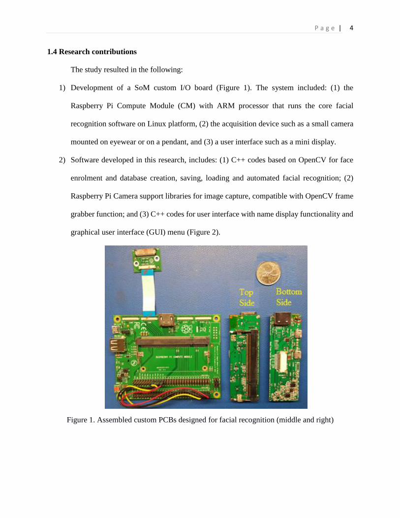
The study resulted in the following:
1) Development of a SoM custom I/O board (Figure 1). The system included: (1) the
Raspberry Pi Compute Module (CM) with ARM processor that runs the core facial
recognition software on Linux platform, (2) the acquisition device such as a small camera
mounted on eyewear or on a pendant, and (3) a user interface such as a mini display.
2) Software developed in this research, includes: (1) C++ codes based on OpenCV for face
enrolment and database creation, saving, loading and automated facial recognition; (2)
Raspberry Pi Camera support libraries for image capture, compatible with OpenCV frame
grabber function; and (3) C++ codes for user interface with name display functionality and
graphical user interface (GUI) menu (Figure 2).
Figure 1. Assembled custom PCBs designed for facial recognition (middle and right)

P a g e |
5
Figure 2. High-level block diagram of the facial recognition device
In summary, the novelty of this work is as follows:
1) The design and implementation of prototype of a wearable embedded solution as a whole
system. It addressed the absence of a standalone autonomous system that would
specifically assist the prosopagnosic patients, and is optimized in size and power
consumption for wearability. The design and implement of this system is one of a kind and
innovative solutions that fulfills the requirements outlined by the prosopagnosia
community at 2012 (no wearable solution was known prior to start of this thesis).
2) Aside from the embedded solution, some of the sub-system solutions that make up this
system are also new. One of them is the design of the DC/DC converter that only uses two-
layer board instead of a board with four layers. This design is also tailored to be powered
by a LiPo battery, with sequencing of the output voltages and protection against over and
under voltage condition.
The Core Face
Recognition
Software on
Embedded
Linux Platform
Acquisition
Device
(Camera)
Module with ARM
Processor
User Interface
(mini display
or
head phones)

P a g e |
6
1.5 Outline of the thesis
This thesis describes the process of designing and testing a prototype for a wearable facial
recognition system for people with prosopagnosia. Chapter 2 provides an overview of the existing
literature on facial detection and recognition technology. A description of the design process for
the wearable device begins in Chapter 3, which examines the development of the proposed
wearable device architecture, including the custom compute module interface. Chapter 4 describes
the design and simulation of a new power section and circuit tests for the wearable device. In
Chapter 5, the software and hardware design process for the wearable prototype is examined, while
Chapter 6 discusses the process of testing the prototype for power consumption, facial recognition
accuracy, and other characteristics. Finally, Chapter 7 provides a summary of the design process
and outcomes, as well as identifies directions for future design work. Additional details on the
prototype design and development process are provided in the thesis appendices.

P a g e |
7
Chapter 2. Literature Review
2.1 Introduction
This chapter provides an overview of the existing literature examining the condition of
prosopagnosia and facial recognition, as well as literature examining previous efforts to develop
computerized face detection and facial recognition systems involving wearable cameras or
devices.
2.2 Prosopagnosia and facial recognition
Facial recognition refers to the cognitive ability of the visual system to discriminate and
identify a specific individual from others by looking at differences in facial features. In humans,
facial recognition is learned at a very early stage of life. Babies develop facial recognition
capacities and are able to recognize their parents (as well as other family members, friends, or even
celebrities) within days of birth to two months [5]. However, about 2.5% of the world’s population
is not able to achieve the task of facial recognition [6]. This cognitive disorder is known as
prosopagnosia, or ‘face blindness’.
In order to aid people with prosopagnosia, a system must be designed to recognize faces.
This computer system must be trained to learn faces for users. When the computer registers a face,
it must recognize and inform the user of the identity of that face.
In the Journal of Cognitive Neuroscience, Turk and Pentland describe the embedded
systems for facial recognition that can be trained to recognize faces. Various techniques may be
used; however, there are generally four main steps, as described in Table 1 [36].

P a g e |
8
Table 1. Four main facial recognition steps and definitions
Step Description
Face detection This process involves locating faces from video frames (and
identifying to whom the faces belongs).
Face preprocessing This process involves adjusting the face image to look clearer,
and scaling it to the same size as other trained faces for facial
comparison.
Face collection and learning
(training)
This process involves saving the preprocessed faces and
learning how to recognize them.
Facial recognition This process involves comparing and identifying the
preprocessed faces from the camera input against the faces in
the database.
2.3 Computerized face detection
According to Chellappa et al., previous research on facial recognition in the field of
computer science and engineering is a well-developed area [7], and many practical applications
have been designed specifically for individual facial identification in security access systems,
human-machine interaction, and dialog-support systems. Many algorithms that use facial modeling
and 3D face matching have been developed, including the popular Eigenface approach, as well as
more sophisticated systems based on principal component analysis and analysis-via-synthesis,
developed by Turk and Pentland [8]. However, a practical facial recognition implementation that
could be used to assist individuals affected by prosopagnosia in recognizing familiar faces has not
yet been developed. In order to better understand how such an implementation could be developed,
two approaches implemented in OpenCV are examined: Haar Feature-based Cascade
Classification techniques, and Local Binary Patterns (LBP).
2.3.1 Facial detection using Haar Feature-Based Cascade Classifier
The first step in facial detection is to identify the object as a face. The literature on object
identification is offered here to gain a better understanding of this first step of the facial recognition
process. The object detector for facial detection described is this section was initially proposed by

P a g e |
9
Paul Viola [9] and improved by Rainer Lienhart [10]. The first approach to facial detection uses
the Haar Feature-Based Cascade Classifier, first training a classifier (a cascade of boosted
classifiers working with Haar-like features) with a few hundred sample views of a particular face.
These include positive examples, which scaled to the same size (for example, 70 x 70), and
negative examples, which are arbitrary images of the same size. After the classifier is trained, it
can be applied to a region of interest (of the same size as used during the training) in an input
image, outputting ‘1’ if the region is likely to show the face (otherwise, it outputs ‘0’). To search
for a face in the whole image, the search window can be moved across the image, checking every
location using the classifier.
The classifier is designed so that it can be easily ‘resized’ in order to find faces of different
sizes, rather than resizing the image itself. To find a face of an unknown size in the image, the scan
procedure can be done several times at different scales. The first check is performed for the coarse
features or structure of a face and if these features match, scanning will continue using finer
features. In each such iteration, areas of the image that do not match a face can be quickly rejected.
The classifier will also keep checking areas for which it is unsure, and certainty will increase in
each iteration that the checked area is indeed a face. Finally, it will stop and make its prediction as
to the identity of the face. This represents a cascading process, with the resultant classifier
consisting of several simpler ones (stages) sequentially applied to a region of interest until all
stages are passed or the candidate is rejected.
The classifiers at each stage of the cascade are built from basic classifiers, using one of
four different boosting techniques (weighted voting). Currently, Discrete Adaboost, Real
Adaboost, Gentle Adaboost, and Logitboost are supported. The current algorithm uses the

P a g e |
10
following Haar-like features. A set of features of a human face is shown in (Figure 3a). When 2a-
2d are combined, for example, a face pattern is produced (Figure 3b).
The feature used in a particular classifier is specified by its shape (1a, 2b, etc. in Figure 3),
position within the region of interest, and scale. For example, in the case of the third line feature
in Figure 3 (2c), the response is calculated as the difference between the sum of image pixels under
the rectangle covering the whole feature (including the two white stripes and the black stripe in
the middle), and the sum of the image pixels under the black stripe multiplied by three in order to
compensate for the differences in area size. The sums of pixel values over a rectangular region are
rapidly calculated using integral images. By gathering statistics about which features compose
faces and how, the algorithm can be trained to use the right features in the right positions and thus
detects faces.
(a) (b)
Figure 3. Human face features (a) and face pattern form (b) combining features from (a)1
2.3.2 Face detection using Local Binary Pattern
The second approach to identifying an object as a face is that of the Local Binary Pattern
(LBP). LBP is a texture descriptor introduced by Ojala et al. [11]. The LBP Histogram (LBPH)
approach (discussed in the following section) focuses on extracting the local features [12, 13, 14],
using the center pixel value as the threshold value. Figure 4 shows an example of an LBP operator.
1http://docs.opencv.org/modules/objdetect/doc/cascade_classification.html?highlight=detectmultiscale#cascadeclass
ifier-detectmultiscale]

P a g e |
11
The LBP operator captures details in an image [14], and features are obtained by combining the
histograms of a LBP image divided into different regions.
Figure 4. Example of an LBP operator
The LBP operator is described by the equation:
𝐿𝐵𝑃(𝑥𝑐, 𝑦𝑐) = ∑ 2𝑃𝑃−1
𝑃=0𝑆(𝑖𝑃 − 𝑖𝑐)
where (xc, yc) is the location of the center pixel, ic is the intensity of the center pixel, P represents
the number of neighbor pixels around the center, ip is the intensity of the current neighbor, and S
is a piecewise function given below:
𝑆(𝑥) = 1 𝑖𝑓 𝑥 ≥ 0 0 𝑖𝑓 𝑥 < 0
The LBP operator results in a new image with certain features such as more enhanced edges. The
new image is then split into non-overlapping sub-regions, and a histogram for each sub-region is
created by mapping color or pixel intensity onto the corresponding number of occurrences of that
color.
2.4 Computerized facial recognition
Facial recognition, or facial classification, involves two major components: training and
recognition. These two processes are discussed in detail below. Training is a process of creating a
template based on a pre-processed (pre-stored) database with correctly identified labels for each
face image. Training for facial recognition is also known as training set generation. Training data
might include data collected off-line or when a person is presented to a video camera at

P a g e |
12
approximately at 15 to 22fps (frames per second). The face is then processed to extract facial
features.
Three main approaches are used to extract or represent facial features: Eigenfaces,
Fisherfaces, and Local Binary Patterns Histograms (LBPH) [12]. When N images are used for
training, the images are transformed into a linear combination of their weight vectors and
Eigenvectors (or Fishervectors or LBPs). Using these vectors, a series of operations are performed:
normalization, weight vector calculation, and projection to Eigenspace (or Fisherspace or LBP
space). This will determine if the features for the presented (probed) face belongs to any of the
individual’s face features in the training data. All three methods perform the recognition by
comparing the probed face with the training set of known faces (Figure 5). In the training set, the
data is labeled with the identity of the faces (Figure 6).
Figure 5. Example of a set of training faces [15]
Figure 6. Facial recognition in operation [36]

P a g e |
13
Given a vector space, the Eigenface and Fisherface approaches are based on a notation of
an orthogonal basis. By combining elements on this basis, one can compose every vector in this
vector space, and every vector in the vector space can also be decomposed into the elements of the
basis. Facial images are often transformed into grayscale 2-dimensional matrices, with each
element corresponding to some intensity level. Matrices are then transformed into one-dimensional
vectors. For example, in a collection of face images measuring 70 x 70 pixels, each image can be
considered a vector of size 4,900 (70 x 70).
The most popular Eigenface method uses Principal Component Analysis (PCA), projecting
images to a vector space with fewer dimensions [16]. A PCA is performed on a feature vector in
order to obtain the eigenvectors, which forms a basis of the vector space. The PCA is an
unsupervised learning algorithm, as training data is unlabeled. When a new unknown face is
presented, it can be decomposed to the basis of the vector space. The found eigenvector
‘represents’ most of the face, thus determining to which person it belongs. The Fisherface method
offers a similar approach, but focuses on maximizing the ratio of between-classes and within-
classes distribution. PCA can be used to reduce dimensionality by capturing facial features that
represent the greatest variance and removing features that correspond to noise. For example, the
PCA-based algorithm [17] computes eigenvalues and eigenvectors from the image database’s
covariance matrix. After ordering eigenvectors, components are projected onto a subspace and
compared to test images using the K-Nearest Neighbor (KNN) algorithm [18].
Templates are used to compare against a current feature vector in order to identify the
probed faces. To create template classes, ordered eigenvectors are found and projected onto the
zero-mean feature vectors. These vectors represent the training database normalized such that the
mean of the intensity is zero. Eigenvectors are defined as 𝜇𝑘 and must satisfy the condition [17]:

P a g e |
14
where C is a covariance matrix defined as , 𝑑𝑖 is the zero-mean feature
vector defined as is the image vector, and 𝑚 is the mean defined as .
The covariance matrix measures the strength of the correlation between the variables. For
face images, this represents the correlation between each image pixel or feature value and every
other image pixel or feature value. The eigenvectors and eigenvalues represent the direction and
strength of the variance, where the first component (largest eigenvalue) has the largest variance.
For face images, the eigenvector represents Eigenfaces that vary from those with the most similar
attributes to those with the largest difference between each face. The Eigenface algorithms
calculate an average face based on all the images in the training set (Figure 7), representing the
mathematical average of all the training images (Figure 7b). Figure 8 shows an example of the first
20 eigenvectors from the training set.
(a) (b)
Figure 7. Original face (left) and average face (right)
Figure 8. Eigenvectors of the dataset
k k kC 1
1 NT
i i
i
d dN
,i iX m X1
1 N
i
i
XN

P a g e |
15
Linear Discriminant Analysis (LDA) is another technique used for feature extraction
distribution, based on the approach described by Belhumeur et al. [19]. As with PCA, LDA
captures features that represent the greatest similarity between faces. However, LDA uses
additional information such as class (each person represents a class, where multiple images of a
person can be stored) to capture features that represent both high similarity and are grouped into
their own class. The equations for between-class distribution matrix and within-class matrix are as
followed [17]:
where 𝑠𝐵 is the between-class scatter matrix, 𝑠𝑤 is the within-class scatter matrix, μ is the total
mean, is the mean of class , and is the current image of class . LDA identifies
eigenvalues and eigenvectors for the scatter matrices instead of the covariance, with scatter
matrices based on the relation of both the total mean and mean within each class.
The Fisherface method uses LDA for facial recognition [19], and LDA has been found to
outperform PCA when dealing with images of varying illumination and expression. An example,
in Figure 9(a), shows the first eight eigenvectors from the training dataset (a) and the first ten
eigenvectors from the dataset (b). Figure 9(b) shows the face transformed following the application
of the Fisherface algorithm to the face from Figure 5.
1
cT
B i i
t
S u u u u
1 k i
cT
W k i k i
t x C
S u u x u
i iC kX iC

P a g e |
16
(a) First eight eigenvectors (b) Local binary patterns from the training set
Figure 9. Training set eigenvectors (a) and LBP (b) from the training set example [15]
(a) Fisher Eigenface (b) Fisher reconstructed face (c) Fisher average face
Figure 10. Face transformation using Fisherface algorithm
During the facial recognition process, Eigenfaces and Fisherfaces examine the dataset as a
whole, to identify a mathematical description of the most dominant features of the entire training
set. The LBPH method takes a different approach, as each image (face) in the training set is
analyzed separately and independently. When a new unknown image is presented, it is compared
to each of the images in the dataset. The images are represented by local patterns in each location
in the image (Figure 9b).
2.5 Approaches to wearable facial recognition
Few prototype solutions for wearable facial recognition have been reported in recent years,
and challenges exist with respect to the practicality of many of these proposed solutions. For
example, in 2005, Wang et al. proposed a wearable facial recognition system for individuals with
visual impairments, with a camera embedded in glasses and connected via USB to a computer for
image processing and face recognition [20]. The computer used the OpenCV library to implement
these tasks. However, this solution delegated image processing and pattern recognition tasks to a
nearby computer, which is impractical for daily use by people with prosopagnosia.
In 2013, a paper on a computerized eyewear-based facial recognition system for people
with prosopagnosia suggested using a camera embedded in glasses with an eyewear display
connected via a video driver board to a smartphone [20]. Online processing could be carried out
on the smartphone using an application that detected and recognized faces on the video sent from
the camera, with information related to the recognized person displayed on the eyewear. However,

P a g e |
17
implementation required that image collection and algorithm training be conducted off-line on a
computer prior to use. The GoogleGlass device has recently been used by some groups for facial
analysis and recognition, although the device is controversial. For example, in 2014 the Fraunhofer
Institute used GoogleGlass as a platform for face detection and facial expression recognition
although no white paper has been published for public access.2 Papers published by Wang et al.
[20], as well as by Krishna et al. [21], have described the use of GoogleGlass as a medium for
taking pictures, with images first detected on GoogleGlass then transferred to the user’s
smartphone via Bluetooth, where images were processed. However, no further developments have
been reported regarding the use of GoogleGlass for facial recognition applications for individuals
with visual or cognitive disorders.
2 http://www.iis.fraunhofer.de/en/pr/2014/20140827_BS_Shore_Google_Glas.html

P a g e |
18
2.6 Conclusion
Previous research has described the challenges associated with facial recognition
technology (reliance on a computer, reliance on being online, having to wear eyewear that
obstructs normal vision, distracting the user) and has emphasized the need for an improvement
with respect to rehabilitation of individuals with prosopagnosia. The facial recognition field is a
well-developed area of study in the area of computer science and engineering, and some standard
steps for facial recognition have been identified. Well-known facial recognition algorithms include
Eigenface, Fisherface, and Local Binary Patterns Histogram. Some published papers and other
sources have described various approaches to address facial recognition challenges among people
with visual or cognitive impairments, including prosopagnosia, by using wearable platforms,
including eyewear displays. However, to date, these studies have not materialized into practical
solutions. The current study aims to address this gap in the field by proposing a practical, wearable
facial recognition solution, assessing its feasibility, and identifying directions for future
development.

P a g e |
19
Chapter 3. Wearable Device Architecture
3.1 Introduction
This chapter describes the proposed architecture of the wearable facial recognition device.
The application system for face detection and recognition is then described, including the design
of the initial wearable prototype. The design of the custom printed circuit board (PCB) is outlined,
followed by a description of the components of the schematics design. The hardware design is
based on the Raspberry Pi Compute Module Development Kit which is designed for developing
embedded application aimed at simplifying the design process. The kit is a complete, time-saving
solution for our wearable device hardware development. It consists of a compute module I/O board
(CMIO), a Raspberry Pi Compute Module (CM), dual display and dual camera adapters.3 With
reference to the design of the IO board, we came up with our own custom board with a smaller
size and better power efficient design.
3.2 The proposed wearable device architecture
The choice of the board for implementation was based on the two main criteria: (1)
appropriate size for a wearable device, and (2) low power consumption with a 5V battery. For
these reasons, the CM was selected for use. This module has physical dimensions of 68mm x
30mm x 1mm / 2.7" x 1.2" x 0.04" and a weight of 5.5g [22].
The custom PCB designed for this project deployed a standard DDR2 SODIMM socket to
house the CM, which is available for purchase in single units, or in batches of hundreds or
thousands. The custom PCB design was inspired by a Computer Module Development Kit, a
prototyping kit (intended for industrial applications) that makes use of the Raspberry Pi in a more
flexible form factor. The CM contains a Raspberry Pi BCM2835 processor, 512Mbyte of RAM,
3 https://www.element14.com/community/community/raspberry-pi/raspberry-pi-compute-module.

P a g e |
20
and a 4Gbyte eMMC Flash device [22]. The Compute Module Input/Output (CMIO) board is a
simple, open-source breakout board that allows for CM plug-in. The CMIO board hosts 120 GPIO
pins, an HDMI port, a USB port, two camera ports, and two display ports (Figure 11) [22].
Figure 11. Compute module development kit, showing the CM and CMIO board [22]
PCB signal routing was performed in order to bring out all the necessary interface signals
specific to the custom design. The custom circuit board design took into consideration the 100-Ω
differential impedance of the HDMI and the 90-Ω differential impedance of the USB signals [23].
A high-efficiency DC/DC converter circuit was designed on a printed circuit board that included
both microUSB and microHDMI connectors, for space saving purposes, although the prototype
(described in Chapter 5) used a larger regular HDMI for ease of manual manufacturability.
The schematics capture and PCB design were performed using the Altium Designer 15
supplied by the Canadian Microelectronic Corporation via a university license [24]. The PCB
board layout design routed out all necessary interface signals for this application.

P a g e |
21
The power section was also completely redesigned. The power section originally used a
two output Diode Inc. PAM2306 chip plus a Low Dropout Regulator (LDO) to achieve the triple-
output voltages required by the Raspberry Pi Compute Module. The power section was redesigned
using a triple-output DC/DC switcher circuit from Linear Technology (LTC3521EUF) to enable
board size downscaling and reduction of component counts.
The current prototype used an off-the-shelf USB Hub board with a USB to Ethernet chip
(such as the Microchip LAN9500 USB-to-Ethernet Controllers) as a low-cost solution. This was
required for loading the Linux OS onto the eMMC flash only. As the OS on the Raspberry Pi
Compute Module may use a different board with this interface, the current interface solution was
proposed for prototype version, not for the final product. To supply power to the board, the
microUSB interface was used to connect the board to a portable power bank. Such a power bank,
normally used for cell phones, is an off-the-shelf solution.
3.3 Embedded Software for face detection and recognition
The embedded solution for face detection and recognition was built using the OpenCV
libraries and the C++ Application Programming Interface (API) RaspiCam [25]. The software
application ran on a fully customized minimum (stripped-down) version of Linux Raspbian
Wheezy from the Raspberry Pi Foundation. This stripped-down version of the OS ran only
necessary functionalities: graphical user interface (GUI), face training, trained data, and facial
recognition (Appendix A). The complete software-to-hardware block diagram for the system is
shown in Figure 12. The following sections describe the facial recognition software and the
hardware design.

P a g e |
22
Figure 12. Hardware-software organization and interface between subsystems [26]
3.3.1 Embedded facial recognition software
Research on facial recognition in computer science and engineering is a well-developed
area. Most facial recognition systems are trained to recognize faces using the following steps: (1)
face detection, (2) face preprocessing, (3) learning faces, and (4) facial recognition. For the current
project, these steps were implemented using embedded C++. The implemented software
application ran on a fully customized version of the Linux operating system. The customized
version of the embedded facial recognition software was fully optimized for low power
consumption and high image processing performance.

P a g e |
23
3.3.2 Hardware design
The proposed system consisted of a Raspberry Pi Camera attached to a Raspberry Pi
Compute Module via a custom-designed PCB. This PCB was a custom-designed I/O board
combining HDMI, power supply input, Raspberry Pi Camera Module input, USB, and composite
video output (Figure 13).
Figure 13. A working prototype performing facial detection
The camera adaptor board used on the reference design was eliminated in order to optimize
board area utilization, reduce final prototype weight, and reduce component cost. Proper
impedance matching and routing were deployed to the new custom PCB board so that the camera
adaptor board was no longer needed (Figure 14).

P a g e |
24
Figure 14. Camera interface board elimination [26]
The core of this prototype system is a Raspberry Pi Compute Module consisting of two
main components: an ARM processor with 512 Megabytes of RAM based on a BCM2835 system-
on-chip (SoC) from Broadcom, and a 4GB eMMC (flash memory with a controller). The SoC also
includes input/output peripheral interfaces. Input-output signals are routed out to copper pads
similar to those on the laptop DDR2 SODIMM memory module with a dimension of 2.7” x 1.2”
x 0.04” (68mm x 30mm x 1mm). This configuration represented a sufficient solution for the
wearable application.
3.3.3 Initial wearable display prototype design
The initial prototype concept consisted of a wearable see-through over-head display with
two reflector see-through lenses. The display image would be projected onto the first set of
reflective lenses and then to the second set before reaching the eyes (Figure 15). The facial
recognition device was located on the right side of the glasses, designed with a small Adafruit Spy
Camera module in one enclosure. Figure 16 shows the first prototype of the see-through over-head
display, with the LCD screen in place (left). A cell phone Mirror Glass Screen Protector was used
to support concept functionality. The mirror was cut to a shape that could be placed onto the two
reflective see-through lenses. This prototype requires further development through testing and
industrial process iterations before becoming truly wearable.

P a g e |
25
Figure 15. Overhead display prototyping
Figure 16. Sketch of the proposed wearable on-eye display
Figure 17 illustrates the system-level block diagram for the proposed wearable device,
showing different design subsections. The core of the design is the SoM, consisting of an ARM
processor and 4 gigabytes eMMC memory for the operating system and application code storage.
Cell Phone
Mirror Screen
Protector Film
Viewing Region
(Person To be Recognized)
LCD
Screen
Augmented Reality Image
with Recognized Person
name & Confidence Level
Overlay on Viewing Region
Camera
Module
Facial
Recognition
Device
Li-Po Batteries

P a g e |
26
Figure 17. System block diagram with CM and surrounding peripheral interfaces [26]
First, the software was tested on a PC with Linux operation system (OS) as well as with
Windows OS. A USB webcam was deployed for use with the PC. When the code was ported to a
Raspberry Pi single-board computer platform, a major performance hit was observed when using
a webcam instead of a Raspberry Pi Camera. The USB webcam produced approximately half
frames per second delay. This delay was measured and benchmarked using a frame-per-second
code. This delay is believed to be due the segmentation and reassembly of the USB packet. In
order to improve video frame processing performance, a Raspberry Pi Camera was selected for
use, with the Pi camera module connected directly to the SoC.
3.3.4 Proof-of-concept for portability
The initial proof-of-concept for portability was done using a prototype involving a
Raspberry Pi 2 single-board computer, Raspberry Pi camera, battery, DC/DC converter, and a
wearable display. The facial recognition device was successfully ported from a PC platform to the
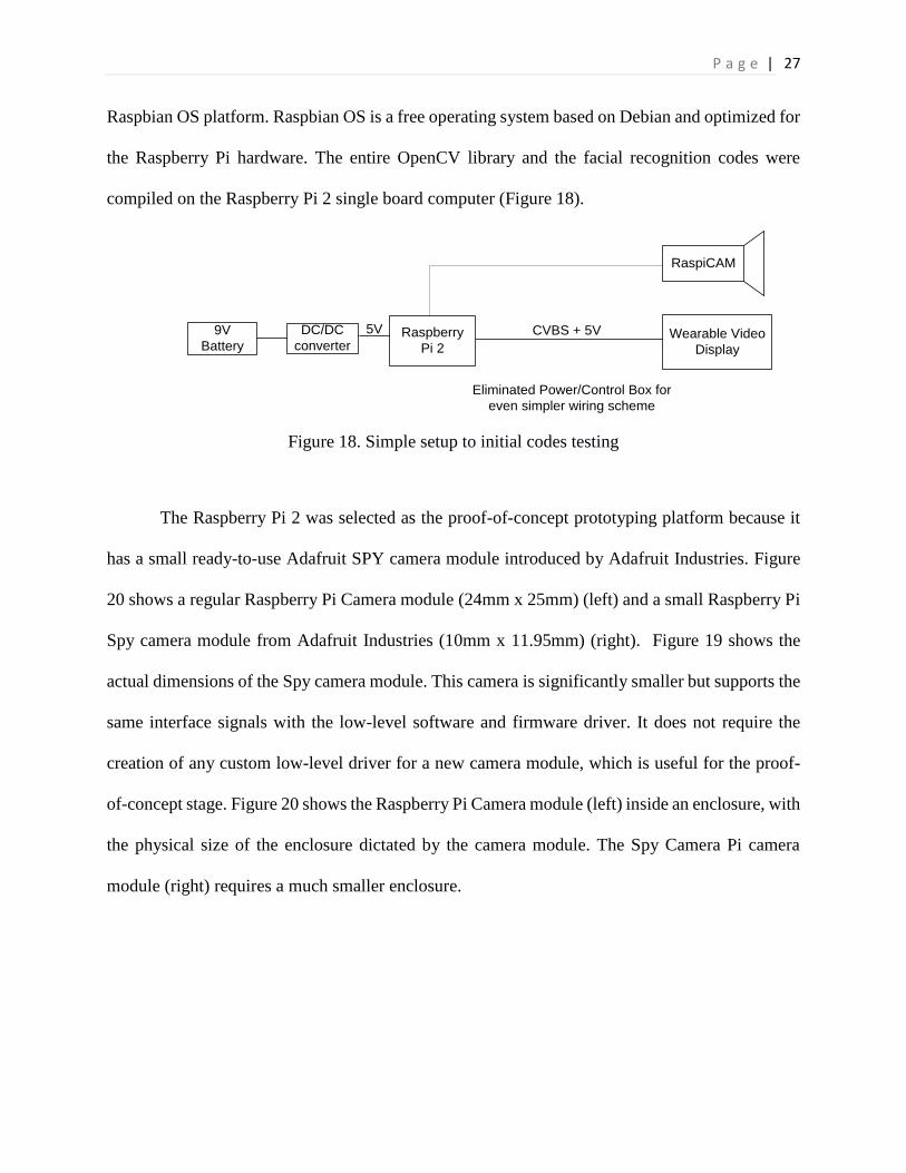
P a g e |
27
Raspbian OS platform. Raspbian OS is a free operating system based on Debian and optimized for
the Raspberry Pi hardware. The entire OpenCV library and the facial recognition codes were
compiled on the Raspberry Pi 2 single board computer (Figure 18).
Figure 18. Simple setup to initial codes testing
The Raspberry Pi 2 was selected as the proof-of-concept prototyping platform because it
has a small ready-to-use Adafruit SPY camera module introduced by Adafruit Industries. Figure
20 shows a regular Raspberry Pi Camera module (24mm x 25mm) (left) and a small Raspberry Pi
Spy camera module from Adafruit Industries (10mm x 11.95mm) (right). Figure 19 shows the
actual dimensions of the Spy camera module. This camera is significantly smaller but supports the
same interface signals with the low-level software and firmware driver. It does not require the
creation of any custom low-level driver for a new camera module, which is useful for the proof-
of-concept stage. Figure 20 shows the Raspberry Pi Camera module (left) inside an enclosure, with
the physical size of the enclosure dictated by the camera module. The Spy Camera Pi camera
module (right) requires a much smaller enclosure.
DC/DC
converter
9V
BatteryWearable Video
Display
CVBS + 5VRaspberry
Pi 2
RaspiCAM
5V
Eliminated Power/Control Box for
even simpler wiring scheme

P a g e |
28
Figure 19. Raspberry Pi Camera module (left) and Spy Camera module (right and bottom) [27]
Figure 20. Raspberry Pi Camera module in enclosure (right) and Spy Camera Module (left)
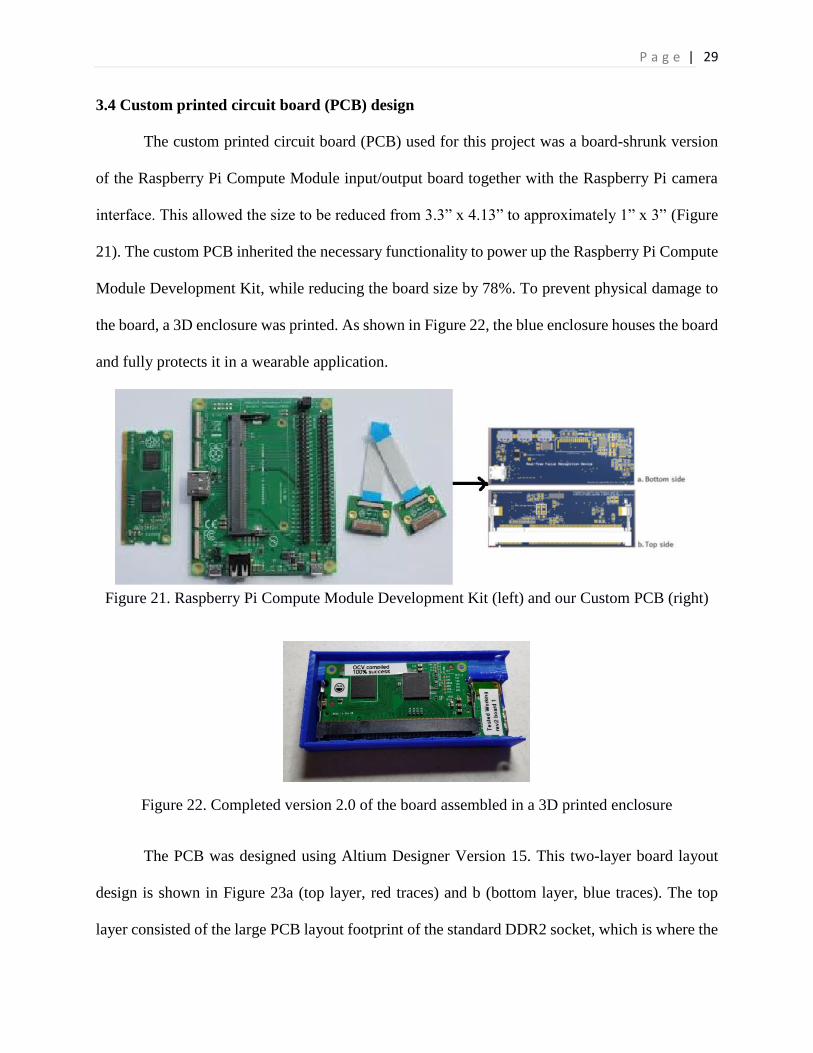
P a g e |
29
3.4 Custom printed circuit board (PCB) design
The custom printed circuit board (PCB) used for this project was a board-shrunk version
of the Raspberry Pi Compute Module input/output board together with the Raspberry Pi camera
interface. This allowed the size to be reduced from 3.3” x 4.13” to approximately 1” x 3” (Figure
21). The custom PCB inherited the necessary functionality to power up the Raspberry Pi Compute
Module Development Kit, while reducing the board size by 78%. To prevent physical damage to
the board, a 3D enclosure was printed. As shown in Figure 22, the blue enclosure houses the board
and fully protects it in a wearable application.
Figure 21. Raspberry Pi Compute Module Development Kit (left) and our Custom PCB (right)
Figure 22. Completed version 2.0 of the board assembled in a 3D printed enclosure
The PCB was designed using Altium Designer Version 15. This two-layer board layout
design is shown in Figure 23a (top layer, red traces) and b (bottom layer, blue traces). The top
layer consisted of the large PCB layout footprint of the standard DDR2 socket, which is where the

P a g e |
30
Raspberry Pi Compute Module would reside. The top layer also contains general-purpose input-
output (GPIO) interface voltage levels selection jumper selection circuits, which allows for the
changing of the system-on-module’s IO interface voltage levels (ARM processor interfaces). The
remaining PCB parts include basic pull-up and pull-down resistors and decoupling capacitors for
signal conditioning, with the blue traces supporting the two USB interfaces (discussed in more
detail in the following section). The left side of the bottom layer of the board contains the power
section, which provides all necessary voltages to the board. The top middle connector is the camera
interface connector, which interfaces with the Raspberry Pi Camera module. On the right side of
the board, there is a USB switch chip that switches between USB programming to upgrade the
operating system image or firmware or normal mode (the device will boot-up normally for facial
recognition). This feature can be enabled by setting the jumper to J4. If there is no jumper on J4,
it will boot up in normal operating mode, which is what the user would see normally for facial
recognition. The right side of the board has an HDMI interface footprint, which is installed for
demonstration purposes and will be removed on the final production revision of the board.
(a) Top Layer (b) Bottom Layer
Figure 23. PCB layout for the custom board showing the top layer (a) and bottom layer (b)

P a g e |
31
Figure 24 shows the similar circuit routing, but with more red area shown meaning that
copper has been poured over the entire board area for better high-frequency noise performance.
This red solid area is usually the system ground (GND). As the original board was a four-layer-
board, a full copper pour is beneficial for better noise performance.
Figure 24. Custom board PCB layout top side with copper poured shown in red
The schematic in Figure 27 shows the Raspberry Pi camera module interface. The
schematic diagrams of the Custom PCB were routed to eliminate the camera interface board. The
traces were routed with differential pairs with differential impedance of 100-Ω.4 The two pairs of
differential data signal pairs (four wires – CAM1D0_N, CAM1D0_P, CAM1D1_N, and
CAM1D1_P) were needed to transmit the camera video frames, and data were synchronized by
the differential pair’s clock signals (CAMK_N and CAMK_P). The CMAIO_N and CAMIO_P
differential pairs were used for the control signals, to control the on/off state of the LEDs on the
Raspberry Pi camera board.
The Raspberry Pi camera has the standard unidirectional low-power, high-speed Mobile
Industry Processor Interface (MIPI) and Camera Serial Interface Type 2 (CSI-2), Versions 1.01,
which connect the BCM2935 and Raspberry Pi Camera Module. The camera interface supports up
to four data lanes, each with a maximum of 1 Gbps bandwidth, for a total bandwidth of 4 Gbps.
Using the Raspberry Pi camera with MIPI interface was found to significantly improve the frame
4 http://techdocs.altium.com/display/ADOH/Differential+Pair+Routing

P a g e |
32
performance compared to a regular USB webcam. The original size of the HDMI on the Raspberry
Pi Compute Module I/O board was a type A full-size HDMI, which is very bulky. For the custom
I/O board, the type D Micro DHMI was used to save board space. The uHDMI is an optional
interface, normally used for demonstration purposes, while an RCA composite video output is
required in most applications.
3.5 Schematics design
The main objective of the schematics design of the custom board was to achieve board
space reduction, battery component selection, and power section redesign while maintaining the
same functionality.
3.5.1 DDR2 connector
The DDR2 connector was used to provide signal interface between the Compute Module
and the custom board. Signals include the camera module interface, USB, HDMI, and composite
video output. Input power lines include the VBAT, 3.3V, 1.8V, VDAC (which is 2.5V), GPIO0-
27_VREF, and GPIO28-45_VREF (Figure 25).

P a g e |
33
Figure 25. DDR2 connector
GPIO28-45_VREF
GPIO46_1V8
GPIO47_1V8
HDMI_CEC
HDMI_SDA
HDMI_SCL
USB_OTGID
TVDAC
RUN
VDD_CORE
GPIO44
GPIO45
GPIO30
GPIO31
GPIO28
GPIO29
GPIO0-27_VREF
USB_D_P
USB_D_N
EMMC_DISABLE_N
HDMI_CK_P
HDMI_D0_P
HDMI_D1_P
HDMI_D2_P
HDMI_CK_N
HDMI_D0_N
HDMI_D1_N
HDMI_D2_N
CAM1_DN0
CAM1_CP
CAM1_CN
CAM1_DP1
CAM1_DN1
CAM1_DP0
GPIO28-45_VREF
GPIO0-27_VREF
11
33
55
77
99
1111
1313
1515
1717
1919
2121
2323
2525
2727
2929
3131
3333
3535
3737
3939
22
44
66
88
1010
1212
1414
1616
1818
2020
2222
2424
2626
2828
3030
3232
3434
3636
3838
4040
4141
4343
4545
4747
4949
5151
5353
5555
5757
5959
6161
6363
6565
6767
6969
7171
7373
7575
7777
7979
8181
8383
8585
8787
8989
9191
9393
9595
9797
9999
101101
103103
105105
107107
109109
111111
113113
115115
117117
119119
121121
123123
125125
127127
129129
131131
133133
135135
137137
139139
141141
143143
145145
147147
149149
151151
153153
155155
157157
159159
161161
163163
165165
167167
169169
171171
173173
175175
177177
179179
181181
183183
185185
187187
189189
191191
193193
195195
197197
199199
4242
4444
4646
4848
5050
5252
5454
5656
5858
6060
6262
6464
6666
6868
7070
7272
7474
7676
7878
8080
8282
8484
8686
8888
9090
9292
9494
9696
9898
100100
102102
104104
106106
108108
110110
112112
114114
116116
118118
120120
122122
124124
126126
128128
130130
132132
134134
136136
138138
140140
142142
144144
146146
148148
150150
152152
154154
156156
158158
160160
162162
164164
166166
168168
170170
172172
174174
176176
178178
180180
182182
184184
186186
188188
190190
192192
194194
196196
198198
200200
J1
DDR2 SODIMM
CM_3V3
CM_VBATCM_VBAT
CM_VDAC CM_VDAC
CM_1V8 CM_1V8
CM_3V3
HDMI_CK_NHDMI_CK_P
HDMI_D0_NHDMI_D0_P
HDMI_D1_NHDMI_D1_P
HDMI_D2_NHDMI_D2_P
CAM1_CPCAM1_CN
CAM1_DP1CAM1_DN1
CAM1_DP0CAM1_DN0
USB_D_PUSB_D_N
HDMI_CECHDMI_SDAHDMI_SCL
Route ringed signals as matched
length 100R differential pairs
Route bold-ringed signals as matched
length 90R differential pair
GPIO 28, 29, 44, 45 DO NOT
HAVE PULLS ENABLED AT BOOT
SO PROVIDE 100K PULL DOWNS
TO AVOID THEM FLOATING
CD1_SDACD1_SCL
CAM1_IO1CAM1_IO0
CD1_SDA
CD1_SCL
CAM1_IO1
CAM1_IO0
TVDAC
Composite Video Output
Need a connector here!!!
R3
060
3 1
00
k
R4
060
3 1
00
k
R6
06
03 1
00
k
R7
06
03 1
00
k
R120603 1k
TP2
GPIO46_1V8

P a g e |
34
3.5.2 Camera module interface
Normally, the camera module would be connected through a Compute Module
Camera/Display Adapter Board (CMCDA). Detailed connections are illustrated in Figure 26, with
the Raspberry PI I/O board on the left, the CMCDA in the middle, and the Raspberry Pi Camera
Module on the right. To optimize space utilization, the schematics design purposely bypassed and
eliminated this CMCDA.
Figure 26. Raspberry Pi camera connection to the Raspberry Pi I/O board [26]
Figure 27 shows the schematics diagram with the signal routing to the SFW15R-2STE1LF
connectors. This connector has a 1mm pin-to-pin spacing, Flexible Flex Cable (FFC), and a
Flexible Printed Circuit made by Amphenol. Each schematics trace was specified with 100-Ω
difference impedance schematic routing and ‘matched-length’ routing for better signal integrity
and enhanced signal quality for face image capture. The signal to the connector pinout was
purposely routed so that the CMCDA could be eliminated altogether.

P a g e |
35
Figure 27. Raspberry Pi camera interface connector and signal
3.5.3 HDMI connection
The AP2331 is a 200mA single-channel current-limited load switch, intended to prevent
overcurrent loading during short-circuit at the HDMI connection (Figure 28 - left). This provides
an interface between the facial recognition device and an external display. The purpose of the
ESD5384, a 5-Line HDMI Control Line ESD chip is for ESD protection, to protect the differential
pairs on the HDMI line (Figure 28 - right).
3V3
CAM1IO_NCAM1IO_P
CD1_SCLCD1_SDA
CAM1
123456789
101112131415
J6
SFW15R-2STE1LF
3V3
CD1_SCL
CD1_SDA
CAM1D0_NCAM1D0_P
CAM1D1_NCAM1D1_P
CAM1C_NCAM1C_P
DIFF100DIFF100
DIFF100DIFF100
DIFF100DIFF100
DIFF100DIFF100
CAM1D0_NCAM1D0_P
CAM1D1_NCAM1D1_P
CAM1C_NCAM1C_P
CAM1IO_NCAM1IO_P
R150805 1K8
R160805 1k8
CD1_SCL
CD1_SDA
CAM1IO_NCAM1IO_P
CAM1D0_NCAM1D0_P
CAM1D1_NCAM1D1_P
CAM1C_NCAM1C_P

P a g e |
36
Figure 28. Current limit load switch (left) and HDMI connection (right)
Connector J7 is a standard-size HDMI connector. The first revision of the board has a micro
HDMI connector, while Revision 2 included an HDMI interface. The micro HDMI is a machine
placed component and is difficult to manually install (solder) the connector under a microscope
with a reflow heat gun. Instead, it is normally placed on the board using a pick-and-place machine
and soldered in place using a reflow oven. Revision 2 of the board involved a standard HDMI
connector for ease of manual manufacturability. During the prototyping phase, it was easier to use
an HDMI interface and to extend the board by half an inch (Figure 29). This second revision of
the facial recognition processing module was found to be fully functional. Revision 2 of the device,
with the Raspberry Pi Camera and regular size HDMI output, is for demonstration purposes only,
in order to demonstrate the working device to a large audience. The HDMI connector will be
removed and an extra half an inch of length reduced during the final design and mass production
phase.
HDMI_CEC
HDMI_HPD
CEC
HDMI_D2_P
HDMI_D2_N
HDMI_D1_P
HDMI_D1_N
HDMI_D0_P
HDMI_D0_N
HDMI_CK_P
HDMI_CK_N
HDMI_SCL
HDMI_SDA
CEC
SCL
SDA
HPD
CEC_VDD
5V
I2C_5V
C2B2
C3B3A3A2
C1B1A1
U3
ESD5384
H5V
3V3
H5V
1V8
HDMI_CEC
HDMI_SCLHDMI_SDA
HDMI_CK_N
HDMI_CK_PHDMI_D0_N
HDMI_D0_PHDMI_D1_N
HDMI_D1_PHDMI_D2_N
HDMI_D2_P
HDMI
R17
0603 2
7k 1
%
R18
0603
100k 1
%
GPIO46_1V8GPIO46_1V8
DIFF100
DIFF100DIFF100
DIFF100DIFF100
DIFF100DIFF100
DIFF100
Q6
DMG1012T
Q4
DMG1012T
123456789
10111213141516171819
20
21
22
23
J7CON_HDMI_RA
GND1
OUT2
IN3
U2
AP2331W
H5V5V
C6
060
3 0
u1F
C70603 0u1F

P a g e |
37
Figure 29. Revision 2 of our facial recognition processing module
3.5.4 I/O voltage selection connector
The DDR2 connector interfaces with the SOC (Figure 25) and has the input-output voltage
selection of 1.8V and 3.3V using the jumper connector. Figure 30 shows the connector bank
voltage operating level. For the current application, an I/O voltage of 3.3V was selected because
all the peripheral attaches to these I/O lines are 3.3V voltage level. For board space reduction, the
composite video output signal was routed to a test point so that no connector is required. The signal
was directly wired to the board.

P a g e |
38
Figure 30. I/O voltage selection circuit
3.5.5 USB interface
The PCB includes two USB interfaces: one for the 5V feed from the power bank, and the
other used to upload trained images or to interface with a keyboard and mouse so that the device
itself could be used to train facial images. The USB switch circuit Figure 31 is used to select
between the USB host and the USB slave. When a USB connection is selected to USB B, it is in
USB slave mode, and the wearable device is connected to a PC so that the entire operating system
can be reprogrammed. When the USB connector is selected to USB A, the device behaves as a
USB host. In USB host mode, a keyboard, a mouse, and a USB storage device can be connected
to the device via a USB hub in order to upload training data from a smartphone or a computer.
GPIO0-27_VREF
GPIO28-45_VREF
1 23 45 6
J3
6W 0.1" PIN HDR
VG0 3V31V8 3V3 1V8VG1
Jumper Positions VG0 / VG1:
1-3 / 2-4 = 3V3
3-5 / 4-6 = 1V8
NC = external source
GPIO BANK 0/1 VOLTAGE SELECT:
R5
0603 0R0
R8
0603 0R0
C10603 1uf 25V X5R
C20603 1uf 25V X5R

P a g e |
39
Alternatively, training images can be downloaded from a USB on-the-go flash drive and
transferred to the wearable device.
Figure 32 shows a jumper connector used to control the USB boot enable. When the USB
boot is enabled, the device will boot from a bootloader located on a PC connected via a USB cable
between the USB B and the PC running RPIBoot.exe.
Figure 31. USB host and slave connection
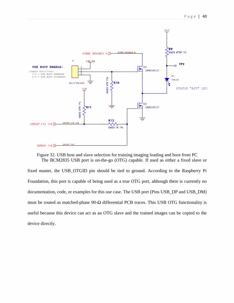
P a g e |
40
Figure 32. USB host and slave selection for training imaging loading and boot from PC
The BCM2835 USB port is on-the-go (OTG) capable. If used as either a fixed slave or
fixed master, the USB_OTGID pin should be tied to ground. According to the Raspberry Pi
Foundation, this port is capable of being used as a true OTG port, although there is currently no
documentation, code, or examples for this use case. The USB port (Pins USB_DP and USB_DM)
must be routed as matched-phase 90-Ω differential PCB traces. This USB OTG functionality is
useful because this device can act as an OTG slave and the trained images can be copied to the
device directly.

P a g e |
41
3.5.6 Video display
The composite video signal is an important signal because it is used to drive the display for
the small overhead display (Appendix D). Thus, the composite video signal can come directly from
the custom board, without any signal condition, translation, or conversion. Figure 33 shows the
display driver board and LCD display (left), as well as the same display mounted inside a custom
designed protective 3D printed enclosure (right).
Figure 33. 1.5” composite video display module (left) and with enclosure (right) [29]
3.5.7 Power section and power management
The PAM2306AYPKE, a Dual DC output step-down converter (DC/DC conversion
switcher), was initially selected to produce 1.8V and 3.3V, while the 2.5V output was produced
by using a low-dropout (LDO) regulator (part number AP7115). The microUSB is an input voltage
interface to the power section (Figure 34), located next to the DC/DC conversion switcher
producing 3.3V and 1.8V. The 3.3V output was also used to feed the LDO to produce 2.5V. Three
low-pass filters were located on the right, to populate any low-pass filter value at a later time with
the proper cutoff frequency targeted to suppress any existing system noise. The inductor initially
used a Bourns SRN4018-4R7M with DC resistance (DCR) of 84mΩ. The initial design for the
device replaced the inductor with Coilcraft’s MSS6132- 472MLB, which has a DCR of 43mΩ.

P a g e |
42
Figure 34. Power section
The Raspberry Pi CM required lower voltage (3.3V and 1.8V), and had to be stepped down
using a DC/DC converter. In order to improve the power efficiency and board space utilization of
the device, another DC/DC converter was proposed. This solution required a custom designed
DC/DC switch mode converter, and the Linear Technology LT3521 IC was selected for use
(discussed in greater detail in the following chapter). The design involving this IC reduced the
board space usage and provided high power efficiency. This was critical to increase the run time
and reduce the weight per watt of battery power delivered to the wearable device, leading to
increase battery life. The high efficiency of this DC/DC converter design meant that very little heat
was dissipated and that the junction-to-ambient temperature rise was well below the converter’s
maximum operating temperature, removing the need for any form of heat sink (adding to device
weight, size, ergonomics, and cost). The intended portable power supply (battery or a power bank)
provides 5V input. A 3D printed enclosure was designed to enable the power bank to be truly
wearable on a belt (Figure 35).
PAM2306AYPKEDual Outputs
DC/DC Converter
3.3V
1.8V
VBAT LDO 2.5VuUSB
LPF
LPF
LPF
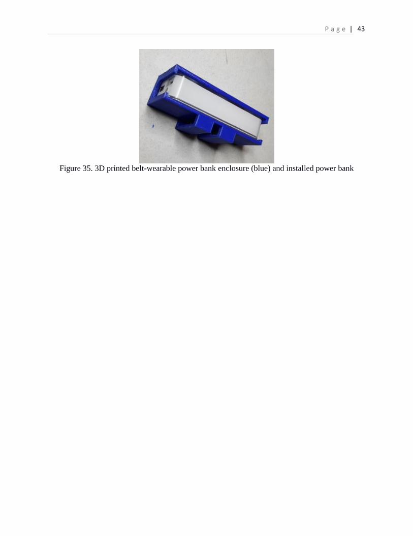
P a g e |
43
Figure 35. 3D printed belt-wearable power bank enclosure (blue) and installed power bank

P a g e |
44
3.6 Conclusion
As described in this chapter, the initial prototype for the wearable facial recognition device
was found to be implementable on a single-board computer (SBC), which makes the idea of
wearability a reality. This board can be powered by a portable battery pack. Inspired by the
Raspberry Pi Compute Module Board and the Raspberry Pi Camera Interface Board, a custom
PCB was designed for board size reduction and improved power efficiency while maintaining the
critical functionality. To ensure portability, a Spy camera module more than four times smaller
than the regular Raspberry Pi Camera Module was used. The complete Raspberry Pi Raspbian
operating system was used to maintain all working low-level drivers (rather than redesigning these
drivers), saving a significant amount of time. The facial recognition code, originally run on the PC
environment, was ported over to the board and recompiled with success. The OpenCV library
codes were recompiled successfully in the Raspbian OS environment. This was considered a
critical achievement in the design, demonstrating that all the software and hardware components
could operate on a wearable platform. The design and simulation of the device’s power section is
described in greater detail in the following chapter.

P a g e |
45
Chapter 4. Power Section Design and Simulation
4.1 Introduction
The design of the custom PCB involved the redesign of the entire power section, to allow
for better power efficiency, smaller circuit surface area, lower components count, higher supply
current, and a wider input voltage range. This chapter describes the power section design and
simulation process, beginning with the initial DC/DC converter evaluations informing power
circuit redesign. The circuit simulation intended to test the design functionality before assembling
the PCB is then outlined, followed by a brief description of the schematics capture and PCB layout
design. The chapter ends with a description of the DC/DC circuit tests.
4.2 Redesigning the power section
The original Compute Module Development kits include a Computer Module and a
Compute Module Input/Output (CMIO) board. The CMIO board uses a dual-output DC/DC
converter, with 3.3V and 1.8V outputs. The 3.3V supply is used to power the BCM2835 processor
core. At the core, it has an internal switched-mode power supply (SMPS) circuit taking in the
voltage and producing the chip core voltage. The 3.3V supply is also used to power BCM2835
PHYs, I/O and the eMMC Flash.5 On the board level, this 3.3V supply is used to power up the
camera module and the USB switch chip; an inefficient Low Dropout Regulator (LDO) is used to
bring the voltage from 3.3V down to 2.5V, functioning as a reference voltage for the core internal
composite video ADC (digital-to-analog conversion) circuit [30]. The 1.8V supply is used to
BCM2835 PHYs, I/O and the SDRAM power [30].
For the custom PCB design, the entire power section was redesigned to allow for better
power efficiency, a smaller circuit surface area, lower components count, a higher supply current,
5 https://www.raspberrypi.org/documentation/hardware/computemodule/cm-designguide.md

P a g e |
46
and a wider input voltage range. The wide input voltage range would accommodate LiPo battery.
The direct power feed from the LiPo to the device is intended for better power efficiency. The use
of the power bank would require a power management module. Currently, the highest efficiency
module is the Texas Instruments BQ24195 charge and power management module, with an
advertised efficiency of 90%.6 The power bank must be connected to another DC/DC converter,
such as the PAM2306, with a reported 89 % efficiency. The resulting efficiency is reduced to
80.1%, since the efficiency of the module connected in series is calculated as 0.90 x 0.85 = 0.81.
This efficiency curve data was measured using an adjustable B&K Precision 8540 DC electronic
load configured to the constant current mode. The efficiency of these components is described in
the following sections.
4.3 Efficiency of PAM2306 DC/DC converter on CMIO
The DC/DC converter used on the CMIO board is the PAM2306AYPKE dual-output
DC/DC converter from Diode Incorporated. The power efficiency of the original DC/DC
converter’s 3.3V output peaks at 89% (Figure 36), while the input voltage range is 2.5V to 5.5V.
As a comparison, efficiency measurements were performed for the original CMIO DC/DC
converter. A graph was plotted as references and comparisons for 3.3V, 1.8V and 2.5V outputs,
which serve as a point of reference for the improvements on the new power section circuit and
PCB design.
4.3.1 Power efficiency for 3.3V output
The efficiency of the power supply was evaluated using the PAM2306 DC/DC converter.
As illustrated in Figure 36, efficiency is highest (89 %) at current draws of 0.15A to 0.3A and it
drops at higher currents, reaching 80 % at 0.78A. This experiment was conducted using B&K
6 http://www.ti.com/tool/bq2419xevm#descriptionArea

P a g e |
47
Precision 8540 DC electronic load, with the current draw first beginning at almost 0A, moving up
to the highest load current before 3.3V fell out of the +/-5 % tolerance. The maximum load was
measured at 780mA.
Figure 36. 3.6V output efficiency peak at 89 %
4.3.2 Power efficiency for 1.8V output
The DC/DC converter’s second output (1.8V) has a power efficiency peak of only 79 %
(Figure 37). This output can provide a maximum current draw of only 350mA. This experiment
was conducted using B&K Precision 8540 DC electronic load, with the current draw first
beginning at almost 0A, moving up to the highest load current before the 1.8V fell out of the +/-5
% tolerance. The maximum load was measured at 340mA.
Figure 37. 1.8V output efficiency peak at 79.5%
35
45
55
65
75
85
95
0 0.2 0.4 0.6 0.8
Effi
cie
ncy
(%
)
3.3V Current Draw (Amp)
0
20
40
60
80
100
0 0.1 0.2 0.3 0.4
Effi
cie
ncy
(%
)
1.8V Current Draw (Amp)

P a g e |
48
4.3.3 Power efficiency for 2.5V LDO output
The 2.5V output was produced from a 3.3V input to a Low Drop Out (LDO) Voltage
Regulator. A LDO is a DC linear voltage regulator that can regulate output voltage even when the
supply voltage is very close to the output voltage. This type of linear regulator is typically not very
efficient when there is a large differential between input and output voltage level, as it works by
taking the difference between the input and output voltages to dissipate it as waste heat. However,
the benefit of using an LDO after the switcher is that it minimizes switching regulator residue in
linear regulator outputs (with linear regulators commonly employed to post-regulate switching
regulator outputs). Benefits include improved stability, accuracy, transient response, and lowered
output impedance.7 While LDO voltage conversion is highly inefficient, it also produces a quieter
output voltage supply. The efficiency of the LDO was found to be only 66 % at 150mA current
draw (Figure 38), with LDO efficiency calculated as: 𝜂 =𝑉𝑂𝑈𝑇
𝑉𝐼𝑁, where 𝜂 is the percentage efficiency
assuming the quiescent current is sufficiently small and can be neglected.8 Although changing the
quieter switcher-to-LDO circuit to a switcher to produce the 2.5V directly presented the risk of
having greater switching noise, the decision was made to use a switcher to produce the 2.5V,
emphasizing efficiency over quietness. Ultimately, this switcher circuit actually performed better
(more quietly) than the LDO solution by means of proper output capacitors deployment without
resorting to any form of output filtering. The switcher solution is described in detail in section
4.5.4.
7 http://cds.linear.com/docs/en/application-note/an101f.pdf 8 http://www.ti.com/lit/an/slva079/slva079.pdf

P a g e |
49
Figure 38. 2.5V LDO output efficiency peak at 66%
4.4 Output ripple of the original PAM2306 DC/DC converter
Understanding the artifacts of output ripple is critical to the DC/DC converter design. The
test and measurement of the output ripple and switching transient is of the utmost importance in
designing low-noise, high-efficiency converters. Measurement techniques included time and
frequency domains analysis, conducted using a 50-Ω end terminated coaxial cable as well as a
Line-Impedance-Stabilization-Network (LISN). The output ripple and switching transient were
measured using an oscilloscope, and ripple levels and harmonics were further confirmed using a
spectrum analyzer.9 These tests served as a comparison baseline for the power section design. The
Raspberry Pi compute module development kit used the output dual ripple of the PAM2306
DC/DC converter. Three voltage levels were tested in the current study: 3.3V, 2.5V, and 1.8V.
The 3.3V and 1.8V outputs were produced directly from the PAM2306 DC/DC converter, while
the 2.5V output was produced by an LDO taking in the 3.3V output.
9 http://www.analog.com/library/analogdialogue/archives/48-08/ripple_measurement.pdf
0
10
20
30
40
50
60
70
0 0.02 0.04 0.06 0.08 0.1 0.12
Effi
cie
ncy
(%
)
2.5V Current Draw(Amp)

P a g e |
50
4.4.1 Output ripple for 3.3V
The 3.3V output ripple is 21.4 milli-volts peak-to-peak. The maximum allowable peak-to-
peak output voltage level is approximately 16.5 milli-volts. This power supply falls into the
acceptable range of the input voltage requirement of the Raspberry Pi Computer Module. The
switching frequency is 1.7MHz (Figure 39). The input voltage is at 3V, but the voltage was swept
across to the supported voltage range and the 3.3V was very stable and within the +/-5 % tolerance.
Figure 39. 3.3V output ripple and switching frequency
4.4.2 Output ripple for 2.5V
As previously mentioned, the 3.3V output was passed through a low-dropout (LDO)
regulator to produce the 2.5V output. Ideally, the output would be expected to be a horizontal line
(Figure 40), but experimental measurement produced an output ripple of 6.45 milli-volts peak-to-

P a g e |
51
peak. This was due to the switching frequency of the 3.3V source conductive frequency emission
through the LDO (Figure 41). In contrast, in the new power section design using LTC3521 chips
and eliminating the LDO, the output ripple was found to be only 4.286mV. While the new design
demonstrated better output ripple performance, both solutions fell within the +/-5 % tolerance. The
LDO requires only input and output capacitors where the output performance is typically believed
to be more superior, although this experiment demonstrated that its output ripple performance is
not always superior to a DC/DC switcher’s output. The PAM2306 plus an LDO solution is noisier
than the proposed triple-output solution, described in the following section 4.5. Without requiring
output low-pass-filter, the switcher equipped with proper output capacitance value can outperform
the LDO in this case. The PAM2306 has a 6.45mVpeak-to-peak ripple, whereas the custom design
using LTC3521 produced a 0.5mVpeak-to-peak ripple under full-load of 600mA.
Figure 40. Conceptual linear regulator and filter capacitors theoretically reject switching
regulator ripple and spikes10
10 http://cds.linear.com/docs/en/application-note/an101f.pdf

P a g e |
52
Figure 41. 2.5V output ripple is 6.45mV peak-to-peak
4.4.3 Output ripple for 1.8V
The Diode Incorporated’s DC/DC converter number PAM2306AYPKE is a dual-output
DC/DC converter, supplying 3.3V and 1.8V. The 2.5V is produced by an AP7115-25SEG, a
150mA LDO linear regular with a shutdown control input signal pin. The 1.8V was found to have
a 7.65mV peak-to-peak output ripple under the no load condition (Figure 42).
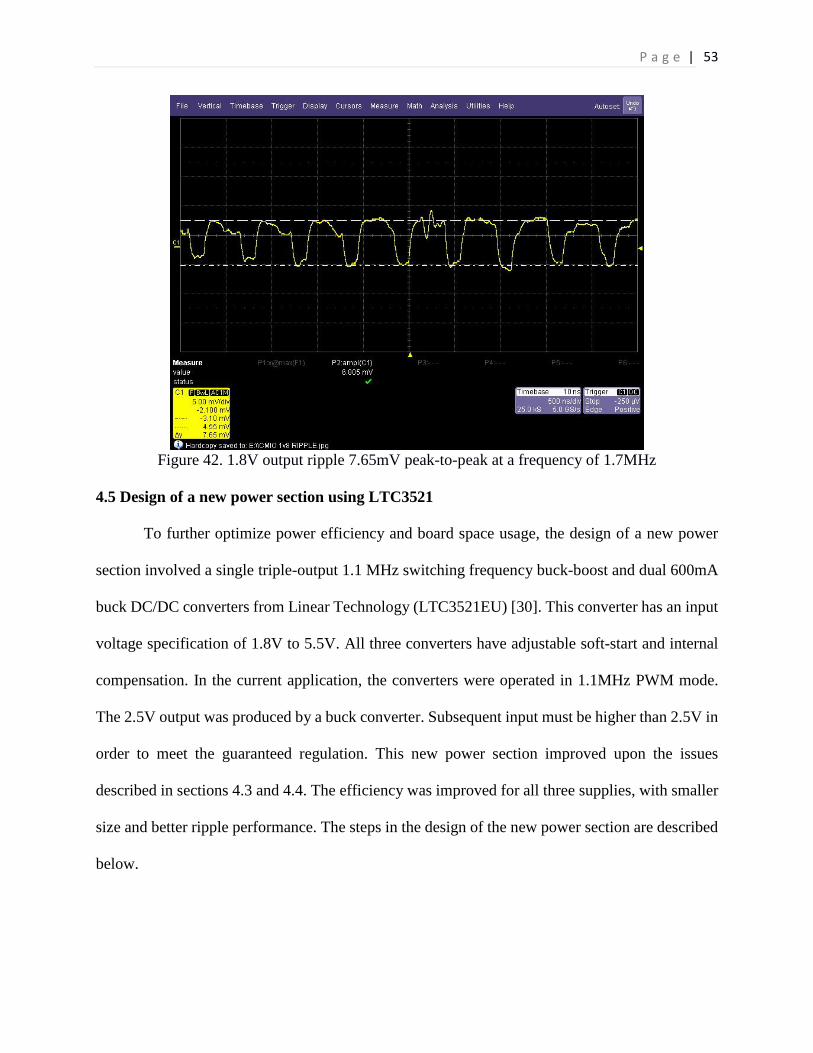
P a g e |
53
Figure 42. 1.8V output ripple 7.65mV peak-to-peak at a frequency of 1.7MHz
4.5 Design of a new power section using LTC3521
To further optimize power efficiency and board space usage, the design of a new power
section involved a single triple-output 1.1 MHz switching frequency buck-boost and dual 600mA
buck DC/DC converters from Linear Technology (LTC3521EU) [30]. This converter has an input
voltage specification of 1.8V to 5.5V. All three converters have adjustable soft-start and internal
compensation. In the current application, the converters were operated in 1.1MHz PWM mode.
The 2.5V output was produced by a buck converter. Subsequent input must be higher than 2.5V in
order to meet the guaranteed regulation. This new power section improved upon the issues
described in sections 4.3 and 4.4. The efficiency was improved for all three supplies, with smaller
size and better ripple performance. The steps in the design of the new power section are described
below.

P a g e |
54
4.5.1 Power circuit design
The design of the application required an IC with triple output capability, more current
capability on all outputs, higher operating efficiency than the existing IC, less supporting
components, smaller packaging size, and wider input voltage that the original DC/DC converter
from Diode Incorporated (PAM2306AYPKE). After a long search, a chip was identified that
fulfilled these requirements: the LTC3521 1A Buck-Boost DC/DC and Dual 600mA Buck DC/DC
Converters from Linear Technology [30], which has two of the three output voltages (Figure 43).
Therefore, the circuit had to be designed to produce 2.5V instead of 1.2V at 600mA. The reason
that we pick this chip is mainly because it is a single chip solution which fulfills our requirement
of three output voltages at a compact size and low passive components count.
Examining the efficiency versus input voltage graph (Figure 43), the ‘marketing efficiency’
of the chip was advertised to be over 94 % at some input voltage. This design was verified by
simulating and testing the circuit’s stability under different input voltages, and a stable constant
current load and varying current load. The varying current load is used to ensure the DC/DC
converter design is able to respond quickly under this transient condition. The circuit was tested
under a different input voltage and output load current. This was to ensure that the output voltage
and ripple were within the tolerance level specified under the computer module hardware design
requirements.
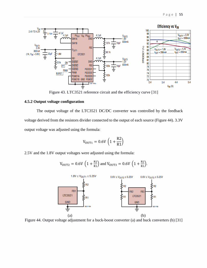
P a g e |
55
Figure 43. LTC3521 reference circuit and the efficiency curve [31]
4.5.2 Output voltage configuration
The output voltage of the LTC3521 DC/DC converter was controlled by the feedback
voltage derived from the resistors divider connected to the output of each source (Figure 44). 3.3V
output voltage was adjusted using the formula:
VOUT1 = 0.6V (1 +R2
R1)
2.5V and the 1.8V output voltages were adjusted using the formula:
VOUT2 = 0.6V (1 +R2
R1) and VOUT3 = 0.6V (1 +
R2
R1).
(a) (b)
Figure 44. Output voltage adjustment for a buck-boost converter (a) and buck converters (b) [31]

P a g e |
56
4.5.3 Power section and output capacitors of the DC/DC converter
According to the datasheet, the LTC3521 DC/DC converter has three output sections. The
output section, where the 3.3V is produced, is a DC/DC buck converter that steps down the voltage
from 5V to 3.3V. It is also capable of boosting the voltage to 3.3V in case the input voltage drops
below 3.3V, with a maximum output current of 1000mA. The other two converter sections,
producing 1.8V and 2.5V, are a buck-converter, which steps down input voltage of 5V. For the
current design, only multilayer ceramic capacitors (MLCCs) were selected for use due to their low
ESR, which is best used for minimizing output voltage ripple. These MLCCs typically come in a
smaller footprint. The 0603 footprint components were used for this design (0805 components can
also be used, although they are slightly larger in size). Larger physical sized capacitors tend to
have lower ESR than smaller counterparts with the same capacitance value.
According to the datasheet, minimum and maximum output capacitor values must be used
to sets the loop crossover frequency. Going beyond this suggested limit would result in an unstable
power supply, where a slight change of load would result in power supply oscillation or resonation.
When the capacitance is too small, “the loop crossover frequency will increase to the point where
the switching delay and the high-frequency parasitic poles of the error amplifier will degrade the
phase margin” [31]. In addition, the wider bandwidth produced by a small output capacitor will
make the loop more susceptible to switching noise. If the output capacitor is too large, the
crossover frequency can decrease too far below the compensation ‘zero’ and lead to a degraded
phase margin. Guidelines for the range of allowable values of low ESR output capacitors are
outlined in Table 2. Larger value output capacitors can be accommodated if they have sufficient
ESR to stabilize the loop [31].

P a g e |
57
Table 2. Recommended capacitance for buck DC/DC converter [31]
Figure 45 shows different frequency responses with various output capacitors. Each
capacitance value is used to suppress various ripples and harmonics frequency at the output of the
DC/DC converters. These tests aim to examine the use different capacitance value to suppress
different harmonics of the DC/DC converter voltage output.
Figure 45. Output capacitors frequency response [32]

P a g e |
58
4.5.4 Maximum outputs current (2.5V output ripple and filtering)
The design takes a 2.4V to 5.5V input voltage. The maximum output current for each
DC/DC controllers was measured as followed: 1.8V at 597mA, 2.5V at 151mA, and 3.3V at 829
mA (Table 3). The DAC_2V5 was initially dropped down from 3.3V to 2.5, using the Digital-to-
Analog Converter (DAC) reference voltage, which is a fairly quiet supply. In the LTspice design,
the peak-to-peak output ripple was found to be 188.054μV for the 2.5V (DAC_2V5) output. These
tests used two 47uF low ESR ceramic output capacitors with X7R temperature coefficient, and a
1210 package size (0.126” x 0.098”) output capacitor mounted in parallel without using the PCB
footprint for a two-stage LC π-filter design. The design was balanced between switching loss and
inductor size. With the switching frequency at 1.1MHz (-74.179dB), the next harmonic was at -
74.98dB. With the input power at 3.54W and 5V input, the expected efficiency is approximately
92.3 %.
Table 3. DC/DC controllers maximum current output tested data
Voltage (Volt) 3.3 2.5 1.8
Maximum current tested (mA) 829 151 597
4.5.5 Cutoff voltage consideration for battery application
In the design, the cutoff was set to 3.0V (Figure 46). The cutoff was required in order to
prevent the battery from exploding when it is over-discharged. For the future design, Li-Po battery
can be used with under voltage lockout at 3.0V. To lockout below 3.0V provides an advantage
because over 90 % of the battery capacitor has been used, and the use of the remaining 10 % would
not be beneficial, as it would present a risk of battery overhead or explosion.

P a g e |
59
Figure 46. Lithium-polymer battery discharge curve with 3.0V cutoff voltage [33]
4.5.6 Inductor selection
According to the datasheet, a reasonable choice for ripple current is ΔIL = 240mA. This
represents 40 % of the maximum load current of 600mA. The DC current rating of the inductor
should be at least equal to the maximum load current, plus half the ripple current, in order to
prevent core saturation and loss of efficiency during operation:
According to the Linear Technology LTC3521 datasheet, the recommended inductance for 2.5V
is at least 4.7µH and at most 8.2µH [31].

P a g e |
60
4.6 LTspice simulation
The design process involved a circuit simulation, intended to test the design functionality.
The simulation was used to determine the theoretical efficiency of the circuit. This allows the
circuit to be proven before being built, thus enabling any design issues and concerns to be
addressed before the actual PCB is produced and assembled. The simulation was conducted using
the Linear Technology LTspice simulation circuit model, illustrated in Figure 47. The LTspice
simulation software is a very powerful simulation package where simulation models for all Linear
Technology solutions can be found, as well as simulations for any general-purpose commonly used
parts. LTspice simulation software is free to download from the Linear Technology website. Using
LTspice, the behavior of the DC/DC converter could be studied and any design issues addressed.
The circuit was simulated under 150mA of constant load on the 2.5V output (Figure 49). The steps
of the simulation are described below.
Figure 47. Schematics of the initial LTspice simulation model

P a g e |
61
Figure 48. LTspice simulation model of the triple outputs DC/DC controller
4.6.1 Crude power sequencing simulation
In this design, the outputs were sequenced as per the Raspberry Pi Compute Module
hardware design requirements. This sequencing was achieved using the output of the 3.3V feeding
to the active low shutdown (SHDN2 and SHDN3) pins of the 1.8V and 2.5V, respectively. The
3.3V SHDN1 pin is connected to the input power (IN), and will come up first once the voltage is
applied at the IN. The active low input signal SHDN3 of 2.5V and the active low input signal
SHDN2 enable the 1.8V to detect the presence the 3.3V, which will in turn command the DC/DC
controller to initiate the 1.8V and 2.5V output. The 3.3V output is stabilized after 158µs.
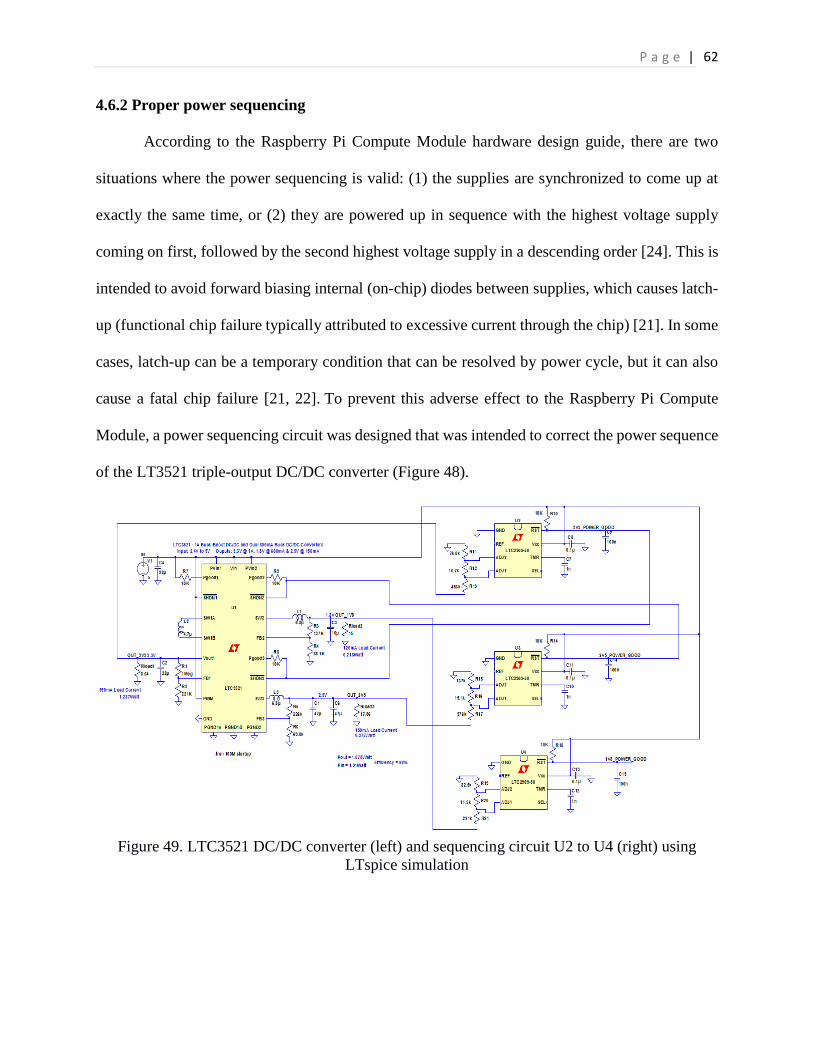
P a g e |
62
4.6.2 Proper power sequencing
According to the Raspberry Pi Compute Module hardware design guide, there are two
situations where the power sequencing is valid: (1) the supplies are synchronized to come up at
exactly the same time, or (2) they are powered up in sequence with the highest voltage supply
coming on first, followed by the second highest voltage supply in a descending order [24]. This is
intended to avoid forward biasing internal (on-chip) diodes between supplies, which causes latch-
up (functional chip failure typically attributed to excessive current through the chip) [21]. In some
cases, latch-up can be a temporary condition that can be resolved by power cycle, but it can also
cause a fatal chip failure [21, 22]. To prevent this adverse effect to the Raspberry Pi Compute
Module, a power sequencing circuit was designed that was intended to correct the power sequence
of the LT3521 triple-output DC/DC converter (Figure 48).
Figure 49. LTC3521 DC/DC converter (left) and sequencing circuit U2 to U4 (right) using
LTspice simulation

P a g e |
63
This power sequencing circuit design works as follows. As the 5V is supplied, 3.3V will
turn on without a constraint, as this is the highest voltage. The U2 will verify if this 3.3V is within
+/-5 % tolerance (in compliance with the hardware design guide). If it falls within the tolerance,
the U2 will issue a 3V3_Power_Good signal to turn on the 2.5V supply through its active low
SHDN3 (shutdown pin). After about 10ms, the 2.5V turns on. The 2.5V output level is then
checked by the U2, which then issues a 2V5_Power_Good signal to turn on the active low SHDN2
of the 1.8V supply. The 1.8V will turn on 10ms later, with the 10ms configured by the TMR pin
of the voltage monitor IC (LTC2909) [25]. The 1.8V is checked by U4 to make sure it falls within
+/-5 % tolerance. The U4 will issue a signal 1V8_Power_Good to an LED status indicator that
confirms that the power section is functioning correctly when the voltage falls within the tolerance
level. As expected, the voltage monitor circuit would not initiate the next voltage in the sequence.
This circuit provides the proper sequencing requirement and serves as a protection circuit to
monitor over-voltage and under-voltage conditions. The power-up sequencing is illustrated in
Figure 50. The higher voltage (3.3V) turns on first, followed by the sequence of lower voltages
(2.5V and 1.8V). All three output voltages are stabilized approximately 1.4ms after power up. The
final solution will be selected for power sequencing.

P a g e |
64
Figure 50. Power sequencing using LTspice simulation
4.6.3 Transient load simulation and testing of the LTC3521 DC/DC converter 2.5V output
The purpose of this test is to confirm that the change in load condition would affect the
DC/DC converter output power supplies. This change of transience could be caused by USB plug
and un-plug. The HDMI insertion and removal would cause the same issue as well. Additionally,
the load would change when the device switched from detection mode to recognition mode where
the current draw is significantly higher. Furthermore, the supply is also able to work properly
initially but handle the initial inrush current during startup with stability.11
The 2.5V design circuit was simulated with 1V steps, using a rapid rise of 1ns for the
duration of 1ms. The circuit was found to hold steady under this load condition. The simulation
plots demonstrated the stability of the circuit under such conditions (Figure 51). The LTC3521
DC/DC converter was equipped with internal compensation for the purpose of minimizing
11 http://www.ti.com.cn/cn/lit/an/slva037a/slva037a.pdf

P a g e |
65
footprint. To ensure that the internal compensation circuit worked correctly for the 2.5V design, it
was tested with a load transient simulation circuit.
Figure 51. 2.5V circuit under test (left) and load transient circuit model (right)
When the output experienced a sudden load change, a 1V transient for the duration of 0.5ms
was recorded (Figure 53). The circuit was observed to react to the change before returning to
stability within 96.8µs (Figure 54). The load transient lab test was performed using the “Line
transient jig with CMOS switching driving two power supplies” figure of the 2013 SN0A895
application report on testing fast response point-of-load (POL) regulators.12 The behavior noted in
the report is similar to that of the simulation results.
12 http://www.ti.com/lit/an/snoa895/snoa895.pdf
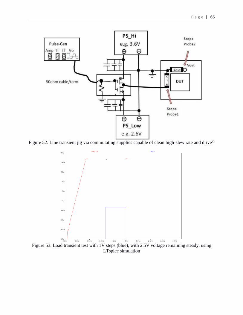
P a g e |
66
Figure 52. Line transient jig via commutating supplies capable of clean high-slew rate and drive12
Figure 53. Load transient test with 1V steps (blue), with 2.5V voltage remaining steady, using
LTspice simulation
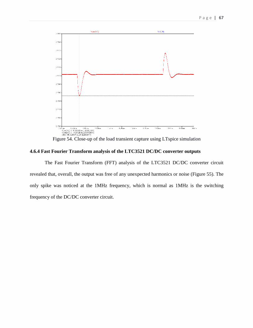
P a g e |
67
Figure 54. Close-up of the load transient capture using LTspice simulation
4.6.4 Fast Fourier Transform analysis of the LTC3521 DC/DC converter outputs
The Fast Fourier Transform (FFT) analysis of the LTC3521 DC/DC converter circuit
revealed that, overall, the output was free of any unexpected harmonics or noise (Figure 55). The
only spike was noticed at the 1MHz frequency, which is normal as 1MHz is the switching
frequency of the DC/DC converter circuit.

P a g e |
68
Figure 55. FFT analysis of the DC/DC converter outputs
4.6.5 Output of the 2.5V LTC3521 DC/DC converter simulation circuit
The LTspice simulation assessed 2.5V output ripple and noise for the LTC3521 DC/DC
converter (Figure 56). The circuit was found to be very quiet, with a 2.5V output ripple at a delta
of approximately 90µV.
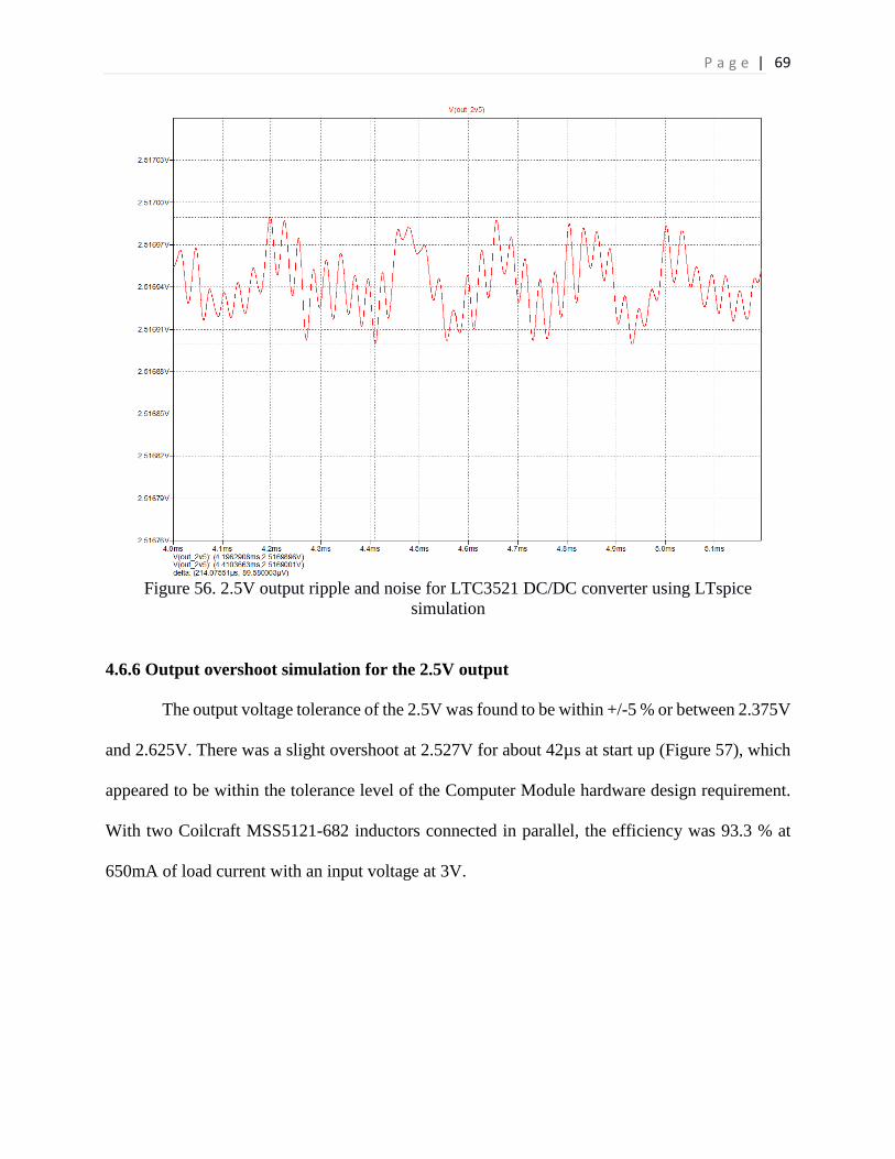
P a g e |
69
Figure 56. 2.5V output ripple and noise for LTC3521 DC/DC converter using LTspice
simulation
4.6.6 Output overshoot simulation for the 2.5V output
The output voltage tolerance of the 2.5V was found to be within +/-5 % or between 2.375V
and 2.625V. There was a slight overshoot at 2.527V for about 42µs at start up (Figure 57), which
appeared to be within the tolerance level of the Computer Module hardware design requirement.
With two Coilcraft MSS5121-682 inductors connected in parallel, the efficiency was 93.3 % at
650mA of load current with an input voltage at 3V.

P a g e |
70
Figure 57. Overshoot at startup at high efficiency using LTspice simulation
4.6.7 Power efficiency simulation
The accuracy of the LTspice simulation depends on the completeness of the passive parts,
including resistors, capacitors, and inductors. A real capacitor would have some equivalent series
resistance (ESR), while an inductor would also have some ESR as well as some parasitic
capacitance. In most cases, a ceramic capacitor has much smaller ESR and can be modeled using
ideal capacitors, which will accept the slight margin of error. The output efficiency of the 1.8V,
2.5V output was found to reach 91.9 %, 93.4 % at maximum load provided a two inductor
connected in parallel, respectively. The power efficiency of the 3.3V output had an efficiency of
86.3 % at maximum load, which is consistent with the graph of actual measurement of 84.3 %.
The efficiency report with root-mean-square current draw, peak current draw, and power
dissipation is illustrated in Table 4.

P a g e |
71
Table 4. Power dissipation on electronics components using LTspice simulation Component
Reference
Irms
Root Mean Square Current
Ipeak
Peak Current
Power
Dissipation
C1, C4, C7, C8, C9 0mA 0mA 0mW
C2 39mA 69mA 0mW
C3 45mA 79mA 0mW
C5 15mA 26mA 0mW
C6 18mA 31mA 0mW
C10 33mA 58mA 0mW
L1 598mA 675mA 36mW
L2 830mA 928mA 45mW
L3 157mA 232mA 2mW
R1 0mA 0mA 7µW
R2 0mA 0mA 2µW
R3 0mA 0mA 10µW
R4 0mA 0mA 5µW
R5 0mA 0mA 16µW
R6 0mA 0mA 5µW
R7 0mA 0mA 0µW
R8 0mA 0mA 0µW
R9 0mA 0mA 0µW
U1 830mA 928mA 267mW
Rload1 829mA 829mA 2748mW
Rload2 596mA 596mA 1066mW
Rload3 151mA 151mA 378mW
In the simulation, input power and output power supplied to the loads (Rload1, Rload2, and
Rload3) added up to 4.192 W (Table 5). This simulation demonstrated the peak output power of the
triple-output DC/DC converter, indicating the input power at 4.54W, as summarized in Table 5.
Table 5. Efficiency report using LTspice simulation
Input Power (5V) 4.54 Watt
Output Power1 (Rload1) 2.748 Watt
Output Power2 (Rload2) 1.066 Watt
Output Power3 (Rload3) 0.378 Watt
Total Output Power 4.192 Watt
Efficiency 92.33 %

P a g e |
72
4.6.8 3.3V output voltage
The simulation indicated that the output noise of the 3.3V power supply was the highest
amongst all output voltages in this design but still fell below the required limit of the Raspberry Pi
Compute Module, 3.3V ± 5 % (or 3.3V ± 165mV peak-to-peak). The switching frequency of the
design was found to be approximately 1 MHz, which has a magnitude of 461.938µV at a phase of
147.852 degrees and a group delay of 74.307nS. The highest noise peak was noted at the switching
frequency of 1MHz, which has a magnitude of -65.29dBm (Figure 58). The frequency analyses of
all three outputs are illustrated in Table 6, while the remaining magnitudes and their corresponding
output voltages are shown in Table 6. By adding sufficient output capacitor, the output ripple of
the 3.3V supply can be reduced. A 22uF output capacitor is introduced to reduce the output ripple
from 2.43mVpeak-to-Peak to as quiet as 139.0 µVpeak-to-peak.
Table 6. Output signals characteristics using LTspice simulation Simulation Signal Name Output Voltage (Volt) Magnitude (dB)
V(Out1) 3.3 -65.29
V(Out2) 1.8 -73.69
V(Out3) 2.5 -74.95

P a g e |
73
Figure 58. Frequency analysis of the LT3521 outputs using LTspice simulation
4.7 Schematics capture and PCB layout
The prototype of the power section was developed using the schematics the Altium
Designer Version 15 PCB design software. The schematics design was followed by the PCB layout
design. The schematics of the custom board closely followed the requirements stated in the
computer module hardware design guide.13 The requirements included: (1) the power section
design with the power sequencing, (2) the circuit supporting module booting and eMMC flashing,
and (3) compute module interfaces such as GPIOs, CSI MIPI Serial Camera interface, USB OTG,
HDMI, and composite video output (TVDAC). On the schematics symbols, the PCB footprint was
modified to be smaller, while the standard USB, HDMI, and display connector were retained.
Standard 100-Ω and 90-Ω impedance requirements were followed for camera and USB interfaces,
13 https://www.raspberrypi.org/documentation/hardware/computemodule/cm-designguide.md

P a g e |
74
respectively. The PCB was fully customized and routed to be a two-layers PCB in order to avoid
cross-talk and to carry the desirable current requirements. The top and bottom sides of the boards
were copper poured for better noise performance, and all components and the necessary signals
were successfully placed and routed on a 1” x 3” board area. The end result was a successful, low-
cost, small-size, and low-noise PCB design that tested fully functional.
4.7.1 Schematics capture
Figure 59 shows the schematic capture of the LTC3521 Triple output DC/DC converter.
Figure 59. Schematics for the LTC3521 DC/DC converter
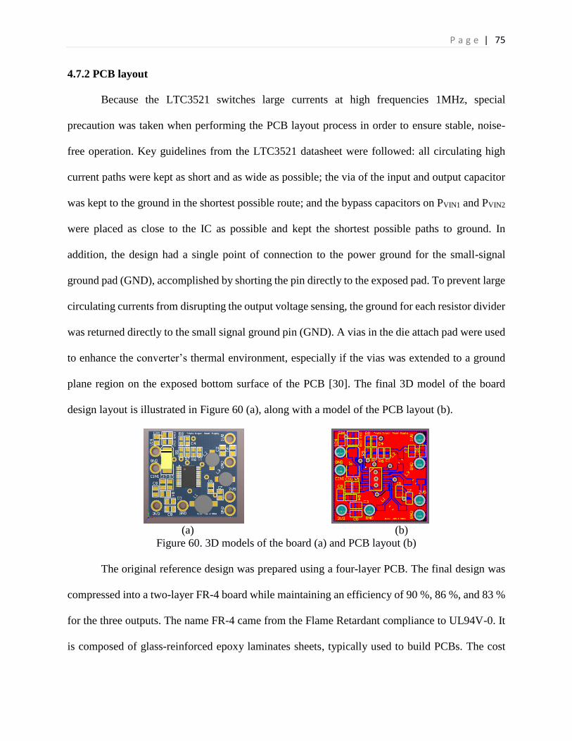
P a g e |
75
4.7.2 PCB layout
Because the LTC3521 switches large currents at high frequencies 1MHz, special
precaution was taken when performing the PCB layout process in order to ensure stable, noise-
free operation. Key guidelines from the LTC3521 datasheet were followed: all circulating high
current paths were kept as short and as wide as possible; the via of the input and output capacitor
was kept to the ground in the shortest possible route; and the bypass capacitors on PVIN1 and PVIN2
were placed as close to the IC as possible and kept the shortest possible paths to ground. In
addition, the design had a single point of connection to the power ground for the small-signal
ground pad (GND), accomplished by shorting the pin directly to the exposed pad. To prevent large
circulating currents from disrupting the output voltage sensing, the ground for each resistor divider
was returned directly to the small signal ground pin (GND). A vias in the die attach pad were used
to enhance the converter’s thermal environment, especially if the vias was extended to a ground
plane region on the exposed bottom surface of the PCB [30]. The final 3D model of the board
design layout is illustrated in Figure 60 (a), along with a model of the PCB layout (b).
(a) (b)
Figure 60. 3D models of the board (a) and PCB layout (b)
The original reference design was prepared using a four-layer PCB. The final design was
compressed into a two-layer FR-4 board while maintaining an efficiency of 90 %, 86 %, and 83 %
for the three outputs. The name FR-4 came from the Flame Retardant compliance to UL94V-0. It
is composed of glass-reinforced epoxy laminates sheets, typically used to build PCBs. The cost

P a g e |
76
ratio between the two-layer and four-layer boards is 1 to 5. The design result was a successful one,
where all three signals tested fully functional with desirable power efficiency, low output ripple,
and stability under full-load and zero-load.
4.8 DC/DC circuit test
After the board assembly was completed, actual power efficiency measurements were
performed to determine the input and output power to the LTC3521 DC/DC converter. These test
results were used to compare the new design and the original PAM2306 DC/DC converter design
on the compute module development kit. Test results demonstrated the improvement of the custom
power section design involving the LTC3521 DC/DC converter. Measurements were performed
using a BK Precision BK8540 and adjustable electronics load. Only one output was tested at a
time, with other outputs disabled by pulling the active low SHUTDOWN_N signal.
4.8.1 Linear Tech LTC3521 DC/DC converter efficiency measurements
As the LTC3521 is a triple-output DC/DC converter, each output voltage (3.3V, 2.5V,
1.8V) was measured with the other two output supplies at the zero-load condition in order to
simplify the process. Measurements were performed using a BK Precision BK8540 and adjustable
electronic load (E-Load), and the 5V input to the board was supplied using a lab power supply
(Figure 61). The current draw beginning at almost 0A, moving to the highest load current before
the 3.3V fell out of +/-5 % tolerance. The efficiency of the power supply for different outputs
(3.3V, 2.5V, 1.8V) was evaluated using the LTC3521 DC/DC converter. The completed circuit
prototype is shown in (Figure 62).

P a g e |
77
Figure 61. LT3521 efficiency measurement setup block diagram
Figure 62. Populated DC/DC switcher PCB under test
4.8.2 Efficiency study of 3.3V output
Efficiency for 3.3V output was found to be the highest (90 %) at current draws of 150mA
to 370mA, and began to drop at higher currents, reaching 80 % at 780mA (Figure 63). The
maximum load was measured at 780mA. This actual measurement was conducted on the populated
PCB with the Linear Technology LTC3521 DC/DC Converter. The original circuit was able to
handle less than 780mA, while the output supply current was capable of handling slightly more
than 1000mA. This can support future releases of hardware such as audio output or additional
processing power.
LT3521 DC/DC Converter
(Device Under Test)
5V Input
3.3V
2.5V
1.8V E-Load
3.3V SHUTDOWN_n
2.5V SHUTDOWN_n
1.8V SHUTDOWN_n
VCC
VCC

P a g e |
78
Figure 63. Efficiency graph for 3.3V output using the LTC3521 DC/DC converter
4.8.3 Efficiency study of 2.5V output
Efficiency for 2.5V output was found to be highest (86.64 %) at current draws of 10mA to
600mA (Figure 64), remaining from 300mA to 600mA. The original design used an LDO taking
in 3.3V from the PAM2306AYPKE, proven to be a low-efficiency approach. While it is a common
practice in the industry to use an LDO as the final stage to produce a quiet supply, this may not be
the best approach when developing a wearable device intended to minimize all power loss without
compromising the requirement of a quiet output. The issue of low-noise design will be addressed
using sufficient output capacitors and possibly pi-filters if required.
0.00
20.00
40.00
60.00
80.00
100.00
0.00 0.20 0.40 0.60 0.80 1.00 1.20
Effi
cie
ncy
(%
)
Load Current (Amp)
Efficiency for 3.3V output

P a g e |
79
Figure 64. Efficiency graph for 2.5V output using the LTC3521 DC/DC converter
4.8.4 Efficiency study of 1.8V output
Efficiency for 1.8V output was found to be highest (83.72 %) at current draws of 10mA to
600mA (Figure 65), remaining stable from 300mA to 600mA. This reflects an improvement in
power efficiency compared to the original circuit (79 %). The original circuit had an output current
of 350mA, whereas the newly designed circuit was capable of handling a load of 600mA.
0.00
10.00
20.00
30.00
40.00
50.00
60.00
70.00
80.00
90.00
100.00
0.000 0.100 0.200 0.300 0.400 0.500 0.600 0.700
Load Current (Amp)
Efficiency for 2.5V Output
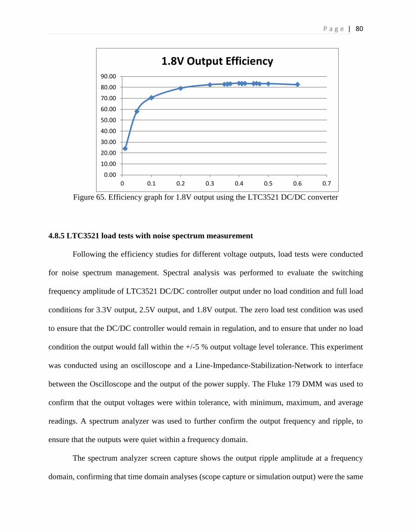
P a g e |
80
Figure 65. Efficiency graph for 1.8V output using the LTC3521 DC/DC converter
4.8.5 LTC3521 load tests with noise spectrum measurement
Following the efficiency studies for different voltage outputs, load tests were conducted
for noise spectrum management. Spectral analysis was performed to evaluate the switching
frequency amplitude of LTC3521 DC/DC controller output under no load condition and full load
conditions for 3.3V output, 2.5V output, and 1.8V output. The zero load test condition was used
to ensure that the DC/DC controller would remain in regulation, and to ensure that under no load
condition the output would fall within the +/-5 % output voltage level tolerance. This experiment
was conducted using an oscilloscope and a Line-Impedance-Stabilization-Network to interface
between the Oscilloscope and the output of the power supply. The Fluke 179 DMM was used to
confirm that the output voltages were within tolerance, with minimum, maximum, and average
readings. A spectrum analyzer was used to further confirm the output frequency and ripple, to
ensure that the outputs were quiet within a frequency domain.
The spectrum analyzer screen capture shows the output ripple amplitude at a frequency
domain, confirming that time domain analyses (scope capture or simulation output) were the same
0.00
10.00
20.00
30.00
40.00
50.00
60.00
70.00
80.00
90.00
0 0.1 0.2 0.3 0.4 0.5 0.6 0.7
1.8V Output Efficiency
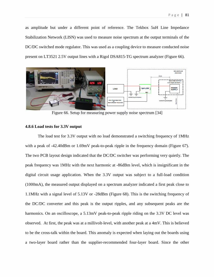
P a g e |
81
as amplitude but under a different point of reference. The Tekbox 5uH Line Impedance
Stabilization Network (LISN) was used to measure noise spectrum at the output terminals of the
DC/DC switched mode regulator. This was used as a coupling device to measure conducted noise
present on LT3521 2.5V output lines with a Rigol DSA815-TG spectrum analyzer (Figure 66).
Figure 66. Setup for measuring power supply noise spectrum [34]
4.8.6 Load tests for 3.3V output
The load test for 3.3V output with no load demonstrated a switching frequency of 1MHz
with a peak of -42.40dBm or 1.69mV peak-to-peak ripple in the frequency domain (Figure 67).
The two PCB layout design indicated that the DC/DC switcher was performing very quietly. The
peak frequency was 1MHz with the next harmonic at -86dBm level, which is insignificant in the
digital circuit usage application. When the 3.3V output was subject to a full-load condition
(1000mA), the measured output displayed on a spectrum analyzer indicated a first peak close to
1.1MHz with a signal level of 5.13V or -28dBm (Figure 68). This is the switching frequency of
the DC/DC converter and this peak is the output ripples, and any subsequent peaks are the
harmonics. On an oscilloscope, a 5.13mV peak-to-peak ripple riding on the 3.3V DC level was
observed. At first, the peak was at a millivolt-level, with another peak at a 4mV. This is believed
to be the cross-talk within the board. This anomaly is expected when laying out the boards using
a two-layer board rather than the supplier-recommended four-layer board. Since the other
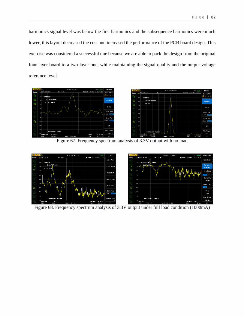
P a g e |
82
harmonics signal level was below the first harmonics and the subsequence harmonics were much
lower, this layout decreased the cost and increased the performance of the PCB board design. This
exercise was considered a successful one because we are able to pack the design from the original
four-layer board to a two-layer one, while maintaining the signal quality and the output voltage
tolerance level.
Figure 67. Frequency spectrum analysis of 3.3V output with no load
Figure 68. Frequency spectrum analysis of 3.3V output under full load condition (1000mA)

P a g e |
83
4.8.7 Load tests for 2.5V output
The 2.5V output circuit tested stable at 2.5V under no load condition (Figure 69). For the
load, the peak output ripple voltage for the 2.5V output was less than 1mV, indicating a very quiet
circuit. When the 2.5V output was subject to a full-load condition (600mA), the spectrum analyzer
indicated the first peak close to 1.1MHz with a signal level of 576.52µV or -51.29dBm (Figure
70). At first, the peak was at a microvolt level, with subsequent peaks representing the harmonics
of the switching frequency. With the first peak already as low as half of a microvolt level, the 2.5V
was a fairly quiet signal as the video module DAC reference voltage.
Figure 69. Frequency spectrum analysis for 2.5V output with no load
Figure 70. Frequency spectrum analysis for 2.5V output under full load condition (600mA)
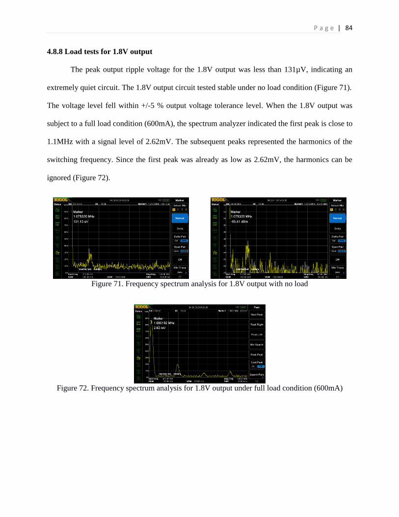
P a g e |
84
4.8.8 Load tests for 1.8V output
The peak output ripple voltage for the 1.8V output was less than 131µV, indicating an
extremely quiet circuit. The 1.8V output circuit tested stable under no load condition (Figure 71).
The voltage level fell within +/-5 % output voltage tolerance level. When the 1.8V output was
subject to a full load condition (600mA), the spectrum analyzer indicated the first peak is close to
1.1MHz with a signal level of 2.62mV. The subsequent peaks represented the harmonics of the
switching frequency. Since the first peak was already as low as 2.62mV, the harmonics can be
ignored (Figure 72).
Figure 71. Frequency spectrum analysis for 1.8V output with no load
Figure 72. Frequency spectrum analysis for 1.8V output under full load condition (600mA)

P a g e |
85
4.9 Conclusion
This chapter describes the design and simulation of the power section of the facial
recognition device. The power supply on the Raspberry Pi compute module development kit’s I/O
board was first tested for efficiency and ripples performance. Load tests, time domain, and
frequency tests were performed, which served as a basis for comparing the new power section.
The design and implementation of the low voltage cutoff and the power sequencing circuit were
also tested.
The power section provided three output voltage values to the Raspberry Pi Compute
Module and other peripheral interfaces, including HDMI, USB, camera module, and display
module. The power section was completely redesigned to use a triple-output DC/DC converter
(LTC3521), in order to optimize size and power efficiency following the evaluation of power
supply and output ripples using the PAM2306 DC/DC converter.
A circuit simulation was conducted using LTspice simulation software, in order to test the
design functionality before assembling the PCB. This involved simulations of power sequencing,
load simulation, output ripple and noise, output overshoot, and power efficiency. DC/DC circuit
tests were conducted, including efficiency measures and load tests at different output voltages. The
three outputs were found to have very low output voltage ripples, falling well within safety levels
and complying with the Compute Module hardware specifications. A prototype of the triple output
DC/DC converter was assembled and tested, and found to have an efficiency of over 90 %, 86 %,
and 83 % (Figure 74), representing an improvement compared to the original DC/DC converters
(Figure 73).
Lithium Polymer3.7V
(4.2V to 3.0V)
Power Manager and
Buck-Booster Circuit
Efficiency 90%
Local Facial Recognition DC/DC Buck Circuit
PAM23062.5V to 5.5V
5V
3.3V
1.8V
LDO 2.5V
Efficiency 81%
Efficiency 71%
Efficiency 59%

P a g e |
86
Figure 73. Existing design
Figure 74. New design
The Raspberry Pi Compute Module requires power sequencing to turn on the highest
voltage output in descending order, and the new design successfully achieved this using the
LTC3521 DC/DC converter. The schematics capture has been completed and a PCB design has
been fabricated and tested with the LTC3521 sequencing circuit. A block diagram of the new
design, involving a power sequencing circuit, is presented in Figure 74. Due to time constraints,
only the circuit simulation has been tested and was fabricated but not populated.
Lithium Polymer3.7V
(4.2V to 3.0V)
Local Facial Recognition DC/DC Buck Circuit
LTC35211.8V to 5.5V
5V
3.3V
1.8V
2.5V
Efficiency 90%
Efficiency 86%
Efficiency 83%

P a g e |
87
Chapter 5. Design of Software and Hardware for the Wearable Prototype
5.1 Introduction
This chapter describes a wearable prototype for the prosopagnosia facial recognition
device. Chapters 3 and 4 presented several solutions to address size, processing speed, and power
efficiency. This chapter describes the final design of the prototype. It provides an overview of the
wearable device prototype design, including the camera and ARM processor interface for running
the facial recognition software under OpenCV and the proposed graphical user interface (GUI),
allowing users to interact with the facial recognition algorithm. This chapter also describes
protection devices intended to prevent electrostatic discharge, overvoltage protection, and
undervoltage protection lockout, while considering privacy issues pertaining to this device.
5.2 Wearable device prototype design overview
A major performance improvement can be achieved by replacing the USB webcam with a
Raspberry Pi camera module. When a USB webcam is used, there is an I/O latency of any standard
USB. With the Raspberry Pi camera module, no CPU overhead is required, so more CPU cycles
are available for core facial recognition application needs.
5.2.1 Camera-to-processor interface connectivity
The Raspberry Pi Compute Module (CM) was the platform selected for this device. This
platform runs on the Raspbian OS, running on a Raspberry Pi single board computer and compute
module. Raspbian is a free operating system based on a Linux variant called Debian, although
Raspbian is optimized for Raspberry Pi hardware.
Low-level driver and API codes are required for the camera interface to the operating
system. It allows for the facial recognition software to receive camera frames from the camera
module and control its hardware. The RaspiCam low-level driver is firmware enabling the

P a g e |
88
Raspberry Pi camera to interface with OpenCV (Appendix E). It provides C++ class RaspiCam_Cv
for the control of the camera within OpenCV code [25]. The Raspberry Pi CM has a Mobile
Industry Processor Interface (MIPI) Camera Serial Interface Type 2 (CSI-2), which facilitates the
connection between the camera and the Broadcom BCM2835 processor [35]. The BCM2835 is an
ARM based SoC. This SoC-to-Camera direct interface option can result in significant performance
improvement when taking camera frames directly from the camera module into the processor. The
use of a Raspberry Pi camera module, connecting directly to the CM, has been widely used for
taking pictures and streaming videos. However, using the Raspberry Pi camera to capture camera
frames within the OpenCV for facial recognition purposes posed a new challenge. To solve this
problem, the RaspiCam library was identified after searching for an open source low-level library.
The library was natively recompiled from source on the CM (Appendix B and C). After several
iterative attempts of RaspiCam library and OpenCV code modifications and software testing, a
video was successfully fed from the CM MIPI camera serial interface onto OpenCV codes for
video frames manipulation and processing. A significant performance improvement of the frame
rate by two to three frames per second was achieved. In addition to contributing to improved
performance, this solution also allowed for a smaller sized camera to be used. The smallest camera
module supported was the Adafruit Spy Camera module (10mm x 11.95mm).
5.2.2 Firmware level greyscale conversion for speed optimization
The greyscale conversion of image frames was originally performed at the software level
in the OpenCV. To further improve the processor’s performance and optimize video throughput,
the RaspiCam low-level library and natively recompiled library C++ code were strategically
modified to allow the firmware to force the video feed into a greyscale format. This convenience
change allowed the facial recognition OpenCV software to the video stream via “/dev/video0”

P a g e |
89
directly in greyscale format without any color-to-greyscale conversion under OpenCV. This
alleviated the software from having to perform OpenCV RGB-to-greyscale conversion algorithm
concurrently with other facial recognition functions.
OpenCV Version 2.4.11 (released in February 2, 2015) was selected for this project
because it is the latest version that supports most operating systems (Windows, Linux/Mac,
Android, and iOS).14 This cross-platform portability allowed the training device to be used on
either a PC computer (as originally planned) or a common platform such as a smartphone or tablet
equipped with a built-in camera module. This version, that supports multiple platforms, also
ensures flexibility in future development, such as the development and release of a smartphone
app (for example, on Android smartphones and as Apple iOS applications).
5.2.3 HDMI to composite video converter elimination
The wearable device was also simplified through the elimination of the HDMI-to-CVBS
(composite) converter, which is shown on the first proof-of-concept block diagram (Figure 75).
The HDMI display was forced to switch off, and the video was directed to the output at the CVBS
interface on the wearable video display. This means that the Raspberry Pi compute module can be
connected directly to the wearable display (Figure 76). The Raspberry Pi OS /boot/config.txt file
was configured to output the signal through HDMI interface by introducing the commands
“sdtv_mode=0”, adding “hdmi_ignore_hotplug=1”, and commenting out
“hdmi_force_hotplug=1”. This forced video output through the CVBS (composite video) output,
instead of allowing video output to HDMI after any system power cycles or reboots. The resolution
14 https://sourceforge.net/projects/opencvlibrary/files/opencv-android/2.4.11/OpenCV-2.4.11-android-
sdk.zip/download
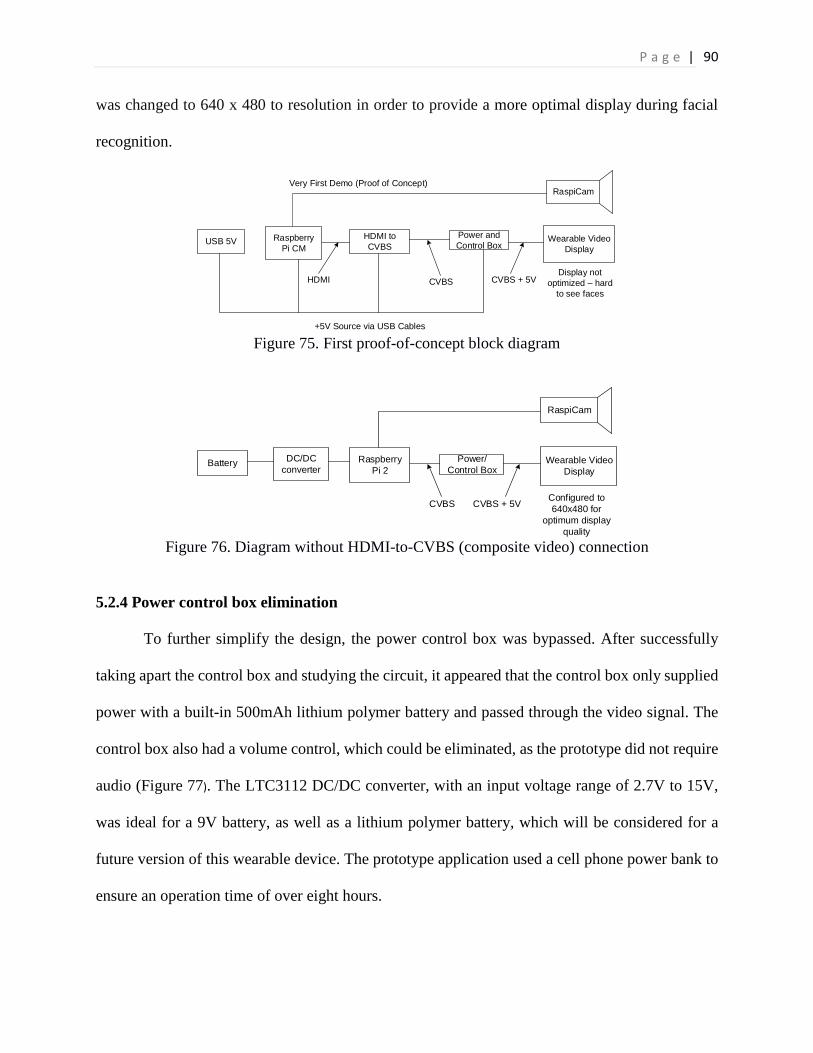
P a g e |
90
was changed to 640 x 480 to resolution in order to provide a more optimal display during facial
recognition.
Figure 75. First proof-of-concept block diagram
Figure 76. Diagram without HDMI-to-CVBS (composite video) connection
5.2.4 Power control box elimination
To further simplify the design, the power control box was bypassed. After successfully
taking apart the control box and studying the circuit, it appeared that the control box only supplied
power with a built-in 500mAh lithium polymer battery and passed through the video signal. The
control box also had a volume control, which could be eliminated, as the prototype did not require
audio (Figure 77). The LTC3112 DC/DC converter, with an input voltage range of 2.7V to 15V,
was ideal for a 9V battery, as well as a lithium polymer battery, which will be considered for a
future version of this wearable device. The prototype application used a cell phone power bank to
ensure an operation time of over eight hours.
USB 5V Wearable Video
Display
Power and
Control Box
HDMI
Raspberry
Pi CM
RaspiCam
CVBS + 5V
HDMI to
CVBS
CVBS
+5V Source via USB Cables
Very First Demo (Proof of Concept)
Display not
optimized – hard
to see faces
DC/DC
converterBattery Wearable Video
Display
Power/
Control Box
CVBS
Raspberry
Pi 2
RaspiCam
CVBS + 5VConfigured to
640x480 for
optimum display
quality

P a g e |
91
Figure 77. Power control box elimination
5.3 Facial Recognition Core Software and GUI
The embedded solution for face detection and recognition was built using the OpenCV
libraries and the C++ Application Programming Interface (API) RaspiCam. The software
application ran on a fully customized minimum version of Linux Raspbian Wheezy from the
Raspberry Pi Foundation. This version of the OS ran only necessary functionalities: graphical user
interface (GUI), face training, trained data, and facial recognition. The achieved facial recognition
functionality was based on a series of standard steps. First, a face was identified in an image frame
using Haar-Cascade classifier and Ada Boost. The identified face was then preprocessed, at which
point it could be easily identified using several well-known facial recognition algorithms such as
Eigenface, Fisherface, and Local Binary Patterns histogram. The source code was tuned to the
specific camera interface being used and optimized to the wearable processor’s low processing
power to maintain processing speed, and power usage was balanced to target at least eight hours
of operating time. The software code was written to automatically load the trained data by default.
The operating system was configured to spawn the facial recognition process upon power-up of
the wearable device, to eliminate any form of user interaction and to improve user friendliness.
When the device is turned on, it is always ready for facial recognition.
DC/DC
converterBattery Wearable Video
Display
CVBS + 5VRaspberry
Pi 2
RaspiCAM
5V
Eliminated Power/Control Box for
even simpler wiring scheme

P a g e |
92
5.3.1 Graphical User Interface
A graphical user interface (GUI) was proposed to make the product user-friendly, by
allowing users to interact with the facial recognition algorithm by adding faces to the training
setup, saving data for future use, recognizing faces, and deleting all trained faces to start over. The
proposed GUI consisted of a control panel, a Frame Per Seconds (FPS) indicator, a confidence
level and name display, a trained faces display, and software mode of operation display (Figure
78).
The control panel, located in the top left corner of the screen, consists of the following
menu: ‘Add Person’, ‘Delete All’, ‘Debug’, ‘Save’, ‘Load’, ‘Recognition’, and ‘Quit’. The FPS
indicator, located beside the control panel, compares the performance of the wearable display
software against the same software code operating in the PC environment in order to compare how
many frames can be processed (by the wearable device and by a desktop PC) in one second.
The GUI included a near real-time confidence level display, indicating the level of
confidence (percentage) with which the face recognition software classified the detected face. This
display was updated for every image frame that included a recognized face, regardless of whether
it was a correct classification (true positive) or a wrong one (false negative). The confidence level
display was linked to the name display, which showed the name of the recognized face and the
associated confidence level. Given that not all frames will be processed when a face is present, the
name and confidence level for the last matched face is displayed. When no face is detected, the
dynamic confidence level indicator will be blank. The static confidence level display will hold the
previous face detection confidence level percentage until the next recognized face. The real-time
display is used for code debugging.

P a g e |
93
All trained faces (faces that the software learns to recognize) are shown on the right side
of the GUI display. All saved faces are stored on a non-volatile NAND flash, even when the device
is powered off. This means that the trained faces will be automatically loaded to the RAM memory
when the device is powered on, so facial recognition can be performed without user intervention.
The mode of operation of the software is indicated at the bottom of the screen. Figure 78
shows the facial recognition software in action. In this image, the software has successfully
recognized the thesis author’s face with an 84 % to 85 % confidence level, regardless of whether
eye-glasses were on or off.
Figure 78. Facial recognition software GUI
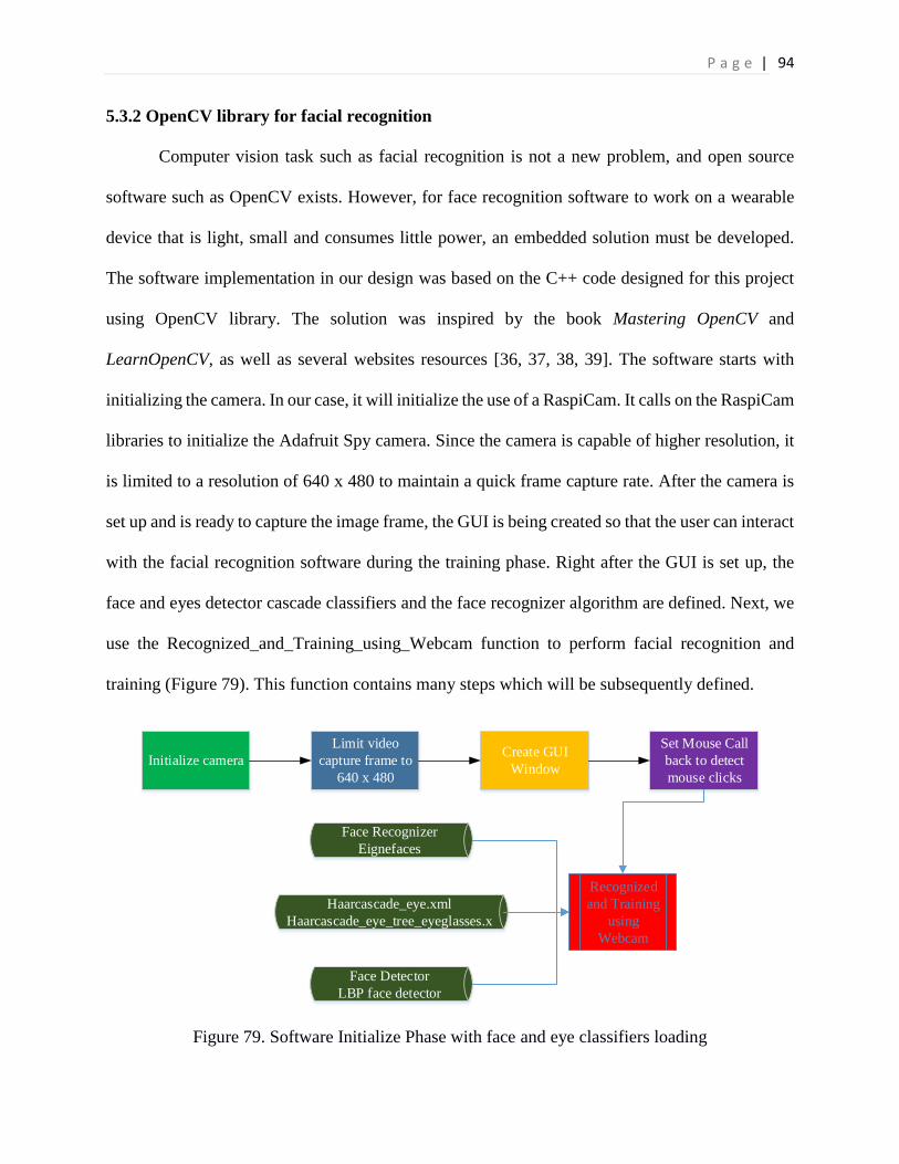
P a g e |
94
5.3.2 OpenCV library for facial recognition
Computer vision task such as facial recognition is not a new problem, and open source
software such as OpenCV exists. However, for face recognition software to work on a wearable
device that is light, small and consumes little power, an embedded solution must be developed.
The software implementation in our design was based on the C++ code designed for this project
using OpenCV library. The solution was inspired by the book Mastering OpenCV and
LearnOpenCV, as well as several websites resources [36, 37, 38, 39]. The software starts with
initializing the camera. In our case, it will initialize the use of a RaspiCam. It calls on the RaspiCam
libraries to initialize the Adafruit Spy camera. Since the camera is capable of higher resolution, it
is limited to a resolution of 640 x 480 to maintain a quick frame capture rate. After the camera is
set up and is ready to capture the image frame, the GUI is being created so that the user can interact
with the facial recognition software during the training phase. Right after the GUI is set up, the
face and eyes detector cascade classifiers and the face recognizer algorithm are defined. Next, we
use the Recognized_and_Training_using_Webcam function to perform facial recognition and
training (Figure 79). This function contains many steps which will be subsequently defined.
Figure 79. Software Initialize Phase with face and eye classifiers loading
Face Recognizer
Eignefaces
Face Detector
LBP face detector
Eye Detector
Haarcascade_eye.xml
Haarcascade_eye_tree_eyeglasses.x
ml
Initialize camera
Limit video
capture frame to
640 x 480
Create GUI
Window
Set Mouse Call
back to detect
mouse clicks
Recognized
and Training
using
Webcam

P a g e |
95
Detailed Explanation of Software Flow
At the start-up of the device, the FaceRecognizer and Cascade Classifiers are loaded,
followed by the initialization of the RaspiCam camera library. The software will first check if a
camera frame is detected. If not, the software will report a problem with the camera, and the
program will quit. If a frame is detected, it will keep a backup copy called displayedFrame
function. The next step is to call on the PreprocessedFace function (Figure 82). The purpose of
this function is to process a face to bring it to a standard size, contrast and brightness. This function
will be explained later with a flowchart and full-description. Once the PreprocessedFace function
execution is complete, it recognizes whether or not there is a face in the video frame. If a face is
present, the face detection counter is incremented, and a rectangle will be displayed around the
detected face. The software will do the same by placing a circle around one or both detected eyes.
Upon completion, it will be ready to check what mode it should be executing next (Figure 80).
First, it will check whether it is in detection mode.

P a g e |
96
Figure 80. Detailed Logic Flow of the Facial Recognition at Software Start-up Stage
END
Grab a camera
frame?
cameraFrame
No
start
Make a copy of the
cameraFrame
called it displayedFrame
Pre-process face
Pre-processsed face
Contain a face data?
GotFace&Eyes=true
Facedetectedcount++
Initialize
GotFace&Eyes=false
yes
FaceRect.width>0Draw rectangle around
detected face
Yes
Check if left eye
are detected?
Check if right eye
are detected?
Draw light-blue
anti-aliased circles
for left eye
Draw light-blue
anti-aliased circles
for right eye
Detection_Mode?
Yes
Yes Yes
No
NoNo
No

P a g e |
97
The flow diagram in Figure 80 is a continuation of that in Figure 79. After both the camera
and the classifier are initialized, the software is in detection mode and checks if the user makes
any change to another mode. If it is in detection mode, the software will display the face and no
other task will be performed. The modes and actions are provided below:
Face Collection Mode
The software will check if the collected face has been previously added to the face database.
If the face image is present in database, the software will add the collected face to the record of
the identified person. If not, it will create a new face ID to store the existing new face. It will check
whether the face is the same as the face from the previous video frame. Otherwise, it will not take
the face for training. Moreover, it will only collect a face every second or every other second to
prevent flooding of the database by too many faces. Only the significantly different faces will be
trained and recorded, and the limit for each post is at least 1 second.
Training Mode
After the faces are collected, the software enters the training mode. In the case of Eigenface
algorithm, the software will take the current collected face and compute an average face using all
the collected instances of this person’s face. In the case of Fisherface, the software will merely add
the current face to the existing database.
Recognition Mode
During recognition mode, the software will take an image from the camera and compare it
against the average faces in the database to determine the highest probability of matching to a face
from the database. The suggestion will be in the form of the face picture, name and the confidence
level of the face that is matched.

P a g e |
98
Delete All Mode
When the software enters this mode, it will delete all the faces in the database.
Load Mode
The face loading mode is to load the faces that have been previously trained and get the
software ready for facial recognition from the flash memory section of the device. This is typically
done right after the device is powered up.
Save Mode
This mode will save all the faces that have been collected and trained. During the
recognition phase, all faces trained are in volatile-memory (RAM). In save mode, the software will
copy the trained faces to the non-volatile-memory (Flash memory). These faces can be loaded
using the load mode on power up.

P a g e |
99
Figure 81. Mode Selection Flow Chart
Detection_Mode?
Mode_Collect_Faces
Mode_Training
Mode_Recognition
Do nothing
Check if face exist
Check if face is different
from previous
w/ noticiple time gap
Check to see if enough data
(Fisherface need at least 2 faces)
If not stay go back to collect
more faces
Reconstruct faces (back projection)
Predict if reconstruct faces = preprocessedfaces(current face on
camera)
If true, recognizePersonCounter++ else unknownperson++
Yes
yes
yes
yes
No
No
No
Mode_Delete_All
No
Mode_Load
Mode_SaveDelete all train
faces
Load Train Faces from
files
Save Train Faces from
files
Yes
Yes
Yes
No
No
No
Start after Camera and
Classifier are loaded
End
(go to Show GUI)

P a g e |
100
At the training phase, we added name entry. We added the saving and loading parts to the
software, and also the facial recognition confidence rate of the person detected with the name
displayed to show identity of whom the software thinks the person is.
When a face is detected, it will be passed onto the PreprocessedFace function where the
face can be preprocessed. The purpose of this preprocessing function is that all the eyes on the face
will be aligned horizontally and the face will be converted to greyscale and histogram equalized.
The implementation block diagram is shown as follows (Figure 82). The full implementation
details including the source codes are described.
Figure 82. PreprocessedFace() Function Implementation Block Diagram
recognizeAndTrainUsingWebcam()
PreprocessedFace()
detectLargestObject()
detectBothEyes()Get centr of eyes
Get angel between eyesGet transformation matrix for rotation &
scalingCv::WarpAffine
(Align face so to both eyes horizontal)
cv::equalizeHist(Perform Histogram Equalization on
either the entire face or individually on each side
cv::bilateralFilter
cv::ellipse(Apply elliptical mask)
cvtColor (faceImg, gray, CV_BGR2GRAY)Greyscale conversion
Return preprocessed Face
detectObjectCustom()
Greyscale conversion
Shrink Image
cv::equalizeHist()
cv::detectMultiscale()
estimated location of typical eyes on a face
(Left Eyes)
estimated location of typical eyes on a face
(Right Eyes)
detectLargestObject() in the region
detectLargestObject() in the region
Return left eyes coordinate
Return right eyes coordinates

P a g e |
101
5.4 Wearable prototype display hardware
The wearable facial recognition device requires a display to show the name of the
recognized subjects. To produce a color display, both display driver components and the display
itself are required. When considering the potential production of the device, some key designs for
manufacturability (DFT) requirements were identified.15
This section examines the ICs used on the display controller board: the A221 Display
Driver IC and the Ultra-Low-Power NTSC/PAL/SECAM Video Decoder, which are described
below. The video decoder takes the composite video output from the facial recognition device and
decodes the video signal into a digital format that the display driver IC can understand. The display
driver takes this decoded signal and maps the pixels on the on-eye overhead display (Figure 83).
Figure 83. Display circuit block diagram
5.4.1 Display drive IC and color display selection
To design the display for the facial recognition device, we used the Kopin A221 Display
Drive IC and the CyberDisplay 230K LV. The A221 Display Drive IC (part number KCD-A221-
BA, Version 0.1 released on August 10, 2006) (Figure 84). The KCD-A221-BA is a display driver
IC that supports Kopin’s low-voltage color displays, including CyberDisplay 113K LV, 152K LV,
230K LV, or WQVGA LV displays.16 The low-voltage 230K CyberDisplay series (part number
KD020230KS) was selected for use in this prototype device. The A221 display driver is designed
to accept a BT.656 or similar digital video source and to generate analog RGB for CyberDisplay
15 http://www.engineersedge.com/training_engineering/why_dfmdfa_is_business_critical_10046.htm 16 http://s1.q4cdn.com/801585987/files/doc_downloads/offerings/VGALVSFeatureSheet.pdf
Small Color
Display
Display
Driver ICVideo Decoder
Facial
Recognition
Device
Composite
Video Signal
Digital
Signals
Digital Signals &
Backlight Power
Control

P a g e |
102
products. It includes three 8-bit DACs, video amplifiers, one charge pump for -5V power supply
voltage to the display, and one PWM current sink control for the backlight. It supports both 2-wire
and 3-wire serial interfaces (Figure 84).17 The summary of information about these components is
shown in Table 7.
Table 7. Critical components for the wearable display
Hardware components Detailed description Manufacturer part
number
On-eye display Cyber Display 230K LV KD020230KS
Display controller/driver IC
(Current prototype)
WQVGA LV Color Displays
Driver IC. The A221 Display
Drive IC series
KCD-A221-BA
Display controller/ driver IC
(Future design consideration)
CyberDisplay WQVGA LVS
Shrink version of the A230K
WQVGA LVS
Figure 84. Kopin display drive IC internal features and architecture18
The current facial recognition prototype design uses the KCD-A221-BA and CyberDisplay
230K LV (KD020230KS), although the WQVGA LVS would achieve an even smaller wearable
17 http://www.itu.int/rec/R-REC-BT.656/en 18 http://www.electronicsdatasheets.com/download/51ab7e0ee34e24e752000077.pdf?format=pdf

P a g e |
103
display. The Kopin WQVGA LVS product line is available as a display/backlight module or as an
optical module, which can be used in conjunction with the A230 driver IC. A low-voltage color
filter display/backlight module will be selected for the wearable device. The low voltage
CyberDisplay WQVGA LVS color filter display/backlight module is an active-matrix liquid
crystal display with 428 240 3 color dot resolution, combined with a white LED backlight. The
display features a low-voltage interface for compatibility with CMOS driver ICs. Both the
horizontal and bidirectional vertical scanner circuits are integrated. A sleep mode is provided to
simplify the system power management.
Figure 85 illustrates the pixel array layout and block diagram of the display module used
for the prototype. Each square full-color pixel is composed of three primary color dots. The active
array of 1284 240 dots is surrounded by opaque dummy pixels, for a total array size of 1308
246 dots. This high-quality display is required to display not only the name of the recognized
subject but also the confidence level for recognition and other GUI information.
Figure 85. Pixel array layout and display module block diagram

P a g e |
104
5.4.2 Ultralow-power NTSC/PAL/SECAM video decoder
The prototype device uses a TVP5150AM1 NTSC/PAL/SECAM video decoder from
Texas Instruments, which comes in a 48-terminal PBGA package or a 32-terminal TQFP package
[38]. The TQFP package was selected because it could be hand-placed and soldered. The
TVP5150AM1 decoder converts NTSC, PAL and SECAM video signals to 8-bit ITU-R BT.656
format. Its optimized architecture allows for ultra-low power consumption, consuming 115-mW
under typical operating conditions and less than 1 mW in power-down mode, which considerably
increases the battery life in portable applications. The TVP5150AM1 decoder uses just one crystal
for all supported standards and can be programmed using an I2C serial interface.19 The
programming is stored on an 8-pin Flash-based, 8-Bit CMOS microcontroller PIC12F683 from
Microchip.
5.4.3 Initial display prototype
The initial prototype was built using the ICs described above, including the Kopin display
module and the display driver and the Texas Instruments video decoder. The design was inspired
by an overhead display from AliExpress.com, the High-quality Virtual Private Cinema Theater
Digital Video Eyewear Glasses 52" Wide Screen with Earphone. The system connection and
components for the initial 3D prototype design are illustrated in Figure 86. At the prototyping
stage, critical components that could be eliminated from the design were identified. The power
interface board, batteries, and power boards were eliminated, as the display would be in close
proximity to the facial recognition processor module, which could provide local clean power to
the display module.
19 http://www.ti.com/lit/ds/symlink/tvp5150am1.pdf

P a g e |
105
Figure 86. Initial prototype system connection and components
Video eyewear (on-eye display) is generally used for entertainment purposes (e.g. watching
movies). As such, the video signal input on the device was too far away from the source, while
providing USB power to the video eyewear would be noisy (potentially affecting the composite
video voltage reference, resulting in voltage jitter that might affect video quality). The composite
signal comes from a very long distance and picks up noise, with a local battery that acts as a signal
conditioning device and stable power reservoir. The current prototype application does not require
local power because the on-eye display is in close proximity to the processor board, and these
power-related boards were therefore eliminated (Figure 87). The board elimination could be
achieved by splicing the same signal together. To confirm that the signal would go through
correctly, a digital multi-meter (DMM) was used to perform a continuity check of the signal and
an oscilloscope was used to ensure the proper signals were correctly connected (Figure 88).
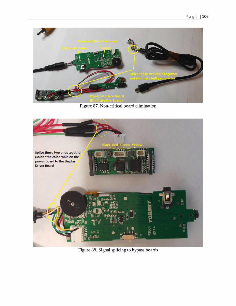
P a g e |
106
Figure 87. Non-critical board elimination
Figure 88. Signal splicing to bypass boards

P a g e |
107
5.4.4 Mechanical/industrial design prototype
The design of the enclosure for the wearable prototype was inspired by existing on-eyes
displays for different applications and hardware, such as wearable video glasses (e.g. Google
Glasses) intended for entertainment purposes. Specifically, the design was modeled using Google
Sketchup and was printed using a 3D printer manufactured by Dremel. The 3D printed enclosure,
made from polylactic acid or polylactide (PLA, Poly), serves to protect the electronic design from
the harsh operating environment of a human body (such as sweat and rough handling), and it is
both convenient and ergonomic. Figure 89 shows a 3D-printed enclosed-housing wearable on-eyes
display.
(a) (b)
Figure 89. Facial recognition module inside the 3D printed enclosure (a), with the on-eye display
attached to eyeglasses (b)
5.5 Transient voltage suppressions and over voltage protection
When a device is worn on a human body, electrostatic discharge (ESD) presents a known
risk. Any failure in the Raspberry Pi Compute Module could lead to a sudden input voltage surge
or ESD event to any of its input ports. As the proposed design is a medical device, it must function
as reliably as possible. To mitigate risks associated with ESD, overvoltage protection, and
undervoltage protection lockout, a number of protection devices were designed for the prototype
device.

P a g e |
108
5.5.1 TVS or Transorb Protection
A wearable device located close to the human body has a higher than normal probability
of experiencing an ESD event compared to a device statically mounted on a building, where a
permanent connection to the earth ground is available. Transient Voltage Suppressor (TVS) ICs
were implemented to protect key device components, including the HDMI output port, the USB
host input port, and the Raspberry Pi camera module interface port.
Two of the TVS ICs considered for use were the TPD4E1U06DBVR and the
TPD45009DBVR from Texas Instruments. These are used to protect high-speed differential pairs.
The ports are connected directly to the SoC IC. Since any ESD hits would damage the core IC of
the wearable device, the protection of these interface lines are crucial. These TVS are used to
protect the USB connection. As for the HDMI protection, the ST Micro HDMIULC6-4SC6Y and
the HDMIULC6-4SC6 are two alternative solutions to protect the HDMI output port specifically.
The HDMI interface signal is connected directly to the SoC IC, and any ESD hits would damage
the core IC of the wearable device. To protect the 3.3V input, the SRDA3.3-4BGT was identified
for use to protect the Raspberry Pi Compute Module’s 3.3V input. This 3.3V protection device is
designed on a custom PCB with 3.3V power rail to ensure it stays stable at 3.3V or lower. It will
conduct when the voltage goes above 3.4V. Without such protection, high voltage will damage the
Raspberry Pi computer module.
5.6 Privacy requirements
This device, in its early development stage, was targeted for early adopters who do not
have concerns about privacy. As an autonomous, standalone device, it functions independently of
any so-called ‘smart’ device and does not require any other hardware. With its own computation
capability, camera module, display, and storage, the device is able to perform both facial

P a g e |
109
recognition and face training. However, if others connected to devices such as smartphones (for
example, to collect images for training), privacy concerns may be raised, similar to those
encountered by most smartphone users who store personal pictures on their smartphones or social
media users who accept that their pictures are publicly available. Being reliant on a smart device
might incur infringements of privacy when gathering images of people, potentially placing the
person’s identity at risk should there be a leak of information.
To address privacy concerns, it is suggested that users delete trained images that are saved
on the smartphone or PC after transmission to the facial recognition device. This would ensure that
the identities of these people are secure. Moreover, in order to obtain this device, careful
examination of the patient’s condition would be required to ensure that only individuals with
prosopagnosia gain access to a device with such strong information storing capabilities. Only
patients with prosopagnosia would be granted permission by a medical official to use this device,
to prevent the misuse of facial recognition information. Once these privacy concerns have been
addressed, the user base of this device may be enlarged to include others who do not suffer from
prosopagnosia; however, initial usage will be restricted to such patients.

P a g e |
110
5.7 Conclusion
The design of a wearable prototype for prosopagnosia facial recognition is an iterative
process. The current prototype solution demonstrates the feasibility of building a wearable facial
recognition device. This chapter has described the design of the software and hardware for the
wearable facial recognition prototype. The Raspberry Pi Compute Module with ARM Processor
was the main platform used for the device. The power section was completely redesigned to
achieve an efficiency of over 90 % and to introduce a more robust power sequencing circuit. The
proposed use of a portable power bank can ensure a practical run-time, while the proposed GUI,
on a stand-alone display, can allow users to train and save faces for convenience and usability. The
user can interact with the GUI display in order to add, save, recognize, or delete faces.
A 3D on-eye enclosure was designed and printed to house the device’s electronic
components in order to prevent damage and to allow for a more realistic operating environment
for the software, camera, and hardware subsystems. Several protection devices were incorporated
in order to prevent electrostatic discharge. To mitigate privacy concerns, the device is intended for
the in-home environment. Following the design process, the prototype was subjected to a series of
experimental tests, which are discussed in the following chapter.

P a g e |
111
Chapter 6. Testing the Prototype
6.1 Introduction
The prototype testing process followed the standard hardware and software test procedures
deployed in the electrical engineering industry.20 We performed power consumption tests to
evaluate the performance of the hardware system in terms of low-power criterion. The face
detection and face recognition rates of the device were tested. Since the device uses video, we
calculated the face detection rate as the ratio of the number of frames with a detected face compared
to the entire number of frames recorded during a limited period of time. The purpose of this chapter
is to assess the performance and accuracy of the performance behaviour of the facial recognition
hardware system and its sub-systems.
6.2 Device power consumption during facial recognition mode
The performance of the device prototype was evaluated in terms of power consumption, as
a low power requirement is one of the objectives. Testing aimed to determine the feasibility of the
wearable design for eight hours of run time.
6.2.1 Raspberry Pi power consumption
The Raspberry Pi Compute Module, running facial recognition and using a Raspberry Pi
camera, is known to have a power consumption of 4.86V at 0.18A to 0.26A current draw, which
provides 0.8748W to 1.26W. With the portable power bank advertised at 4400mAh, this device
lasts for 14.36 hours with a 15 % de-rating (Table 8). This 15 % de-rating is believed to be due to
the power bank’s undervoltage protection (UVP) circuitry and DC/DC converter efficiency, which
converts the lithium polymer battery voltage to 5V of constant voltage output. The experiment
20 https://cdn.rohde-schwarz.com/pws/dl_downloads/dl_application/application_notes/1td04/1TD04_0e_RTO_DC-DC-Converter.pdf
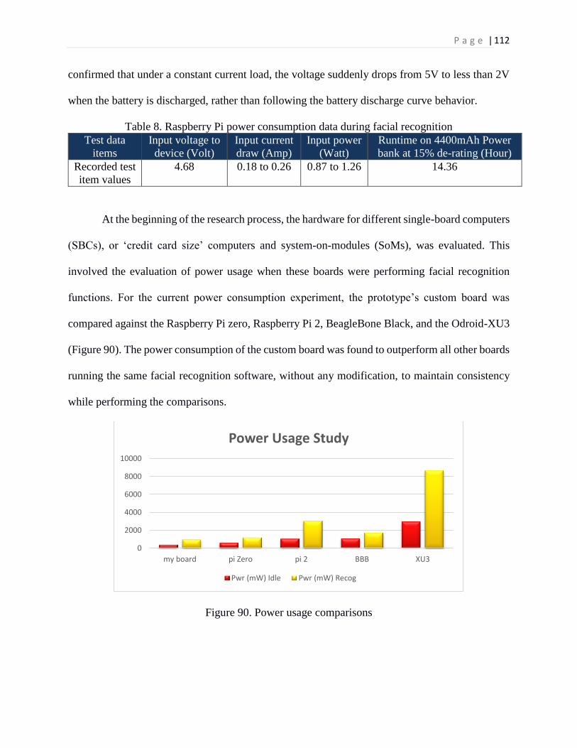
P a g e |
112
confirmed that under a constant current load, the voltage suddenly drops from 5V to less than 2V
when the battery is discharged, rather than following the battery discharge curve behavior.
Table 8. Raspberry Pi power consumption data during facial recognition
Test data
items
Input voltage to
device (Volt)
Input current
draw (Amp)
Input power
(Watt)
Runtime on 4400mAh Power
bank at 15% de-rating (Hour)
Recorded test
item values
4.68 0.18 to 0.26 0.87 to 1.26 14.36
At the beginning of the research process, the hardware for different single-board computers
(SBCs), or ‘credit card size’ computers and system-on-modules (SoMs), was evaluated. This
involved the evaluation of power usage when these boards were performing facial recognition
functions. For the current power consumption experiment, the prototype’s custom board was
compared against the Raspberry Pi zero, Raspberry Pi 2, BeagleBone Black, and the Odroid-XU3
(Figure 90). The power consumption of the custom board was found to outperform all other boards
running the same facial recognition software, without any modification, to maintain consistency
while performing the comparisons.
Figure 90. Power usage comparisons
0
2000
4000
6000
8000
10000
my board pi Zero pi 2 BBB XU3
Power Usage Study
Pwr (mW) Idle Pwr (mW) Recog

P a g e |
113
All the boards were powered by the same fully charged power portable power bank,
measuring 1.65" x 0.9" x 3.9" (42mm x 23mm x 100mm) and weighing about 140g. This power
bank enabled the facial recognition device to be a truly mobile and wearable device. With a USB
hub, USB-to-Ethernet interface, keyboard, and mouse installed, the power bank is estimated to
draw a current of about 0.48A at 5V when the face recognition device is used for face training.
6.2.2 Battery discharge testing
The complete design of a wearable device requires an actual battery discharge test
electrically loaded by running a real-life facial recognition application. This load test involved
training the device on the faces of five individuals and running the facial recognition mode on one
picture in the five-person database for 5.5 hours, using a used lithium polymer Samsung Galaxy
Note cell phone battery (i9220 3.7V 3080mAh High-Capacity Gold Battery). Two 3.7V lithium
polymer cell phone batteries were used in series. The cell voltage display was illustrated as per-
cell voltage under resistive load (Figure 91), with the voltage divided by two for easy
understanding of the battery characteristics under the true load in this facial recognition
application. The battery lasted for 5.5 hours before the device protection circuit shut down the
battery power connection to prevent possible battery explosion. The battery label of mAh is not
always accurate, or perhaps it is used for marketing purposes only.

P a g e |
114
Figure 91. Lithium polymer cell phone battery discharge curve under real device load
6.3 Face detection and recognition accuracy
The device’s performance in terms of facial recognition efficiency was preliminarily
assessed for on-line training and subsequent facial recognition for a small set of subjects. The
system was tested using an on-line video capture of six identities, including two real people and
four taken from a magazine cover. The resolution of the images was 640 x 480, and the cropped
facial images were grey-scaled and scaled down to 80 x 60 pixels for faster processing.
6.3.1 Face detection testing
The device’s face detection performance was assessed by the percentage of frames in which
each face was successfully detected using Haar cascades. The device detected faces when the test
subject did not move, and when the face was in front of the camera, depending on illuminance,
distance, and whether the subject was facing the camera or looking to the side. Experimental results
indicated that the device detected, on average, 96 faces in every 100 frames. The optimal
illuminance for face detection was about 420 lux (Table 9). The lux is the SI unit of illuminance
0
0.5
1
1.5
2
2.5
3
3.5
4
4.5
0.00 1.00 2.00 3.00 4.00 5.00 6.00
Cel
l Vo
ltag
e (V
olt
)
Time (hour)
LiPo Battery Discharge Under Face Recognition Mode

P a g e |
115
and luminous emittance, measuring luminous flux per unit area21. The face detection rate was 98
% in an indoor environment with relatively good lighting during the two-minute video recording.
The Raspberry Pi camera was able to detect faces in 80 % of cases even with poor lighting or in a
semi-dark environment.
Table 9. Face detection rates in different lightning conditions Face Detection Rate Condition Brightness (Lux)
98% Good Light 420
80% Poor Light 210
Face detection rates varied with distance between the device’s camera and the test subject,
with the best detection rate (between 78 % and 96 %) occurring at about two feet away (Table 10).
Detection rates were lower at distances of four feet (approximately 43 % to 60 %), and the camera
could not detect faces at six feet away.
Table 10. Face detection rates by distance and face position
Distance between
face and camera
Face detection rate when
subject faces the camera
Face detection rate when the face is at a 30°
angle to the side
2 feet away 90% 78%
4 feet away 60% 43%
6 feet away 0% 0%
According to proxemics, a distance of about two to four feet between the prosopagnosia
patients and the social interaction space is sufficient (Figure 92). To further enhance the device’s
face detection rate, optical lenses will be required. This design feature will be implemented for
future improvements, if necessary.
21 SI Derived Units, National Institute of Standards and Technology
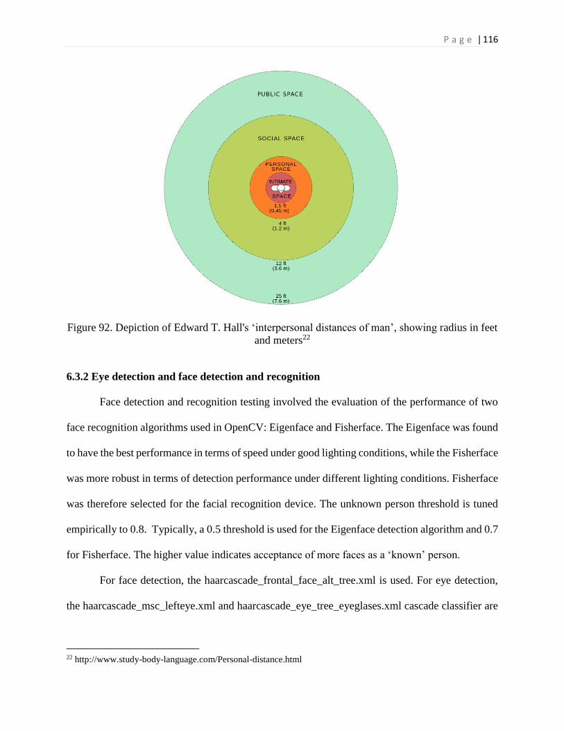
P a g e |
116
Figure 92. Depiction of Edward T. Hall's ‘interpersonal distances of man’, showing radius in feet
and meters22
6.3.2 Eye detection and face detection and recognition
Face detection and recognition testing involved the evaluation of the performance of two
face recognition algorithms used in OpenCV: Eigenface and Fisherface. The Eigenface was found
to have the best performance in terms of speed under good lighting conditions, while the Fisherface
was more robust in terms of detection performance under different lighting conditions. Fisherface
was therefore selected for the facial recognition device. The unknown person threshold is tuned
empirically to 0.8. Typically, a 0.5 threshold is used for the Eigenface detection algorithm and 0.7
for Fisherface. The higher value indicates acceptance of more faces as a ‘known’ person.
For face detection, the haarcascade_frontal_face_alt_tree.xml is used. For eye detection,
the haarcascade_msc_lefteye.xml and haarcascade_eye_tree_eyeglases.xml cascade classifier are
22 http://www.study-body-language.com/Personal-distance.html

P a g e |
117
used. The experimental results on recognition rate (when the face is matched to the correct person
in the database) are represented by confidence levels. Table 11 contains the test data for a database
of six people each trained for one minute.
Table 11. Facial recognition Rate Test after 60 seconds of training
Person # Frame
processed
# true matches
(true positive)
# of false matches
(false positive)
Average
confidence level
for true matches
Average
confidence level
for false matches
1 60 60 0 88% -
2 60 59 1 89% 30%
3 60 58 2 85% 33%
4 60 57 3 82% 29%
5 60 58 2 86% 35%
6 60 56 4 87% 34%
6.3.3 Testing the platform performance on a photo database
The testing of platform performance involved training the subject s1 at 1.pgm, using
AT&T’s The Database of Faces.23 After training on one of the photos, the device was presented
with nine other photographs of the same subject. The result indicated that all photographs were
detected and recognized as true positives with an average confidence level of 62 %. This
experiment was performed with four other trained faces in the device’s database.
6.4 Power consumption and thermal characteristics
The prototype device’s power consumption was found to be 1.26W during facial
recognition mode. This mode has the highest power consumption. When the system-on-chip (SoC)
is running full-speed during the facial recognition phase, it has a temperature of 38.6°C, operating
at 25°C ambient, indicating a temperature rise of 13.6°C. This experiment is recorded using the
23 http://www.cl.cam.ac.uk/research/dtg/attarchive/facedatabase.html

P a g e |
118
author’s FLIR One for iOS thermal imager attached to an iPhone 6. The FLIR thermal imaging
camera shows the hottest spot is the SoC, not the power supply section (Figure 93).
Figure 93. Thermal imaging camera reading of the system-on-chip IC
6.5 System latency
The prototype system latency was evaluated, assessing the delay between the image capture
and the final face detection, face recognition, and display. The facial recognition compiled code
was profiled to identify the specific functions consuming the most processing power. First, the test
stub codes were used to compute the system clock ticks between ‘before’ and ‘after’ the
‘PreprocessedFace’ function. The result was then subtracted and converted to seconds. System
latency was found to be approximately 950ms, with most of the processing time spent on the
‘PreprocessedFace’ C++ function. This was confirmed by using the Linux code profiling tool
(Linux open source GPROF GNU profiler), which indicated that the preprocessed face function
accounted for most of the computing resources. The call graph indicated that the preprocessed face
function was executed 74.72 % of the time with respect to the rest of the codes (Figure 94).

P a g e |
119
Figure 94. Facial recognition code profiling
Main96.77%
recognizedAndTrainUsingWebcam90.19%
getPreProcessedFace74.72%
detectBothEyes15.18%
detectLargestObject74.47%
videoCapture 7.76%
detectObjectsCustom74.47%
CascadeClassifier::detectMultiscale72.28%
Cv::resize::detectMultiscale5.07%
cvHaarDetectObjectsForROC12.06%
cv::detectMultiscale5.07%
51
x
cv::CascadeClassifier::detectSingleScale50.76%
LoopBody57.63%
EX
IT

P a g e |
120
6.6 Conclusion
The experimental testing of the prototype device confirmed that the facial recognition
software could run on a single system-on-module that consumes up to 1.2W from a portable power
bank. All battery powered wearable devices require the primary source of DC power to be
efficiently converted to achieve the longest possible runtime. The design of this wearable facial
recognition device requires a balance between speed, efficiency, and size. For proof-of-concept,
OpenCV was successfully recompiled on this target board. The functionality of the codes was
tested on the Raspberry Pi Compute Module platform, utilizing a miniature Raspberry Pi Spy
camera. A PCB was produced with better power efficiency and a smaller size.
This study has investigated all the steps required to create a near real-time face recognition
application using basic algorithms. With sufficient preprocessing, it allows some differences
between the training set conditions and the testing set conditions. In this implementation, the
device uses face detection to find the location of a face within the camera image, followed by
several forms of face preprocessing to reduce the effects of different lighting conditions, camera
and face orientations, and facial expressions. The machine-learning system is trained using an
Eigenface or Fisherface system with the preprocessed faces collected. Finally, the system performs
face recognition to identify the person, with face verification providing a confidence metric in the
case of a face that is unknown to the system (i.e. not in database). Rather than providing a
command-line tool that processes image files offline, the system combines these steps into a self-
contained near real-time GUI program to allow for immediate use of the face recognition system.
The behavior of the system can be modified for special application purposes, such as automatic
login to the user’s computer or improvement on recognition reliability.
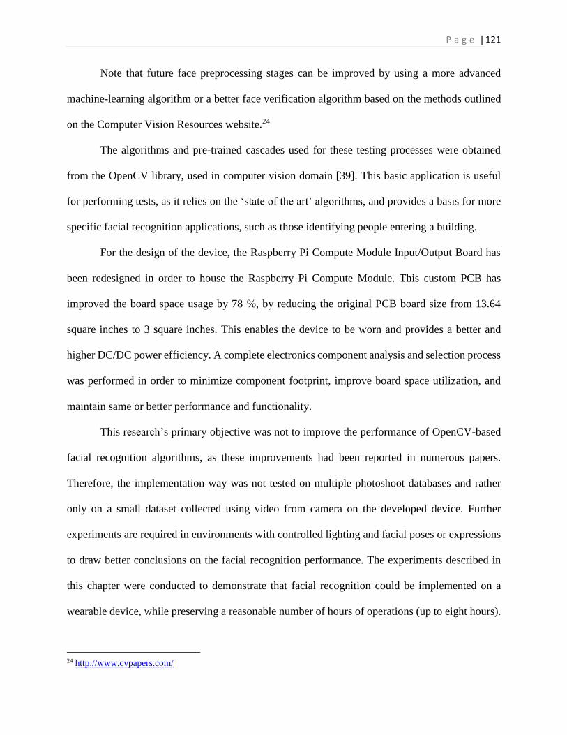
P a g e |
121
Note that future face preprocessing stages can be improved by using a more advanced
machine-learning algorithm or a better face verification algorithm based on the methods outlined
on the Computer Vision Resources website.24
The algorithms and pre-trained cascades used for these testing processes were obtained
from the OpenCV library, used in computer vision domain [39]. This basic application is useful
for performing tests, as it relies on the ‘state of the art’ algorithms, and provides a basis for more
specific facial recognition applications, such as those identifying people entering a building.
For the design of the device, the Raspberry Pi Compute Module Input/Output Board has
been redesigned in order to house the Raspberry Pi Compute Module. This custom PCB has
improved the board space usage by 78 %, by reducing the original PCB board size from 13.64
square inches to 3 square inches. This enables the device to be worn and provides a better and
higher DC/DC power efficiency. A complete electronics component analysis and selection process
was performed in order to minimize component footprint, improve board space utilization, and
maintain same or better performance and functionality.
This research’s primary objective was not to improve the performance of OpenCV-based
facial recognition algorithms, as these improvements had been reported in numerous papers.
Therefore, the implementation way was not tested on multiple photoshoot databases and rather
only on a small dataset collected using video from camera on the developed device. Further
experiments are required in environments with controlled lighting and facial poses or expressions
to draw better conclusions on the facial recognition performance. The experiments described in
this chapter were conducted to demonstrate that facial recognition could be implemented on a
wearable device, while preserving a reasonable number of hours of operations (up to eight hours).
24 http://www.cvpapers.com/

P a g e |
122

P a g e |
123
Chapter 7. Summary and Future Work
7.1 Summary
This study resulted in the successful hardware and software design and implementation of
a wearable prototype system for prosopagnosic patients. Software design involved three areas of
improvement:
1) fine-tuning the operating system, footprint minimization, and performance
optimization and improvement;
2) importing Linux drivers and libraries to allow the streaming of image frames from the
Raspberry Pi camera onto OpenCV functions, as well as fine-tuning, configuring, and
forcing video display to the composite video output with the correct resolution and
frame rate of the wearable display;
3) developing, modifying, and optimizing facial recognition software using OpenCV open
source libraries and codes.
The implementation is based on image processing and pattern recognition algorithms
embedded into a compact-scale processor, such as the Raspberry Pi. It uses the techniques
implemented in OpenCV (open source computer vision library). The custom PCB-based I/O
hardware solution with the Raspberry Pi Compute Module is optimized for size and has a power
efficiency of over 90 %, compared with 77 % for a non-custom Raspberry Pi I/O board with the
same CM. This solution makes the prototype design wearable when using a 5V portable power
bank or a 3.6V lithium polymer battery. In addition, we suggest five optimal designs of the PCB
I/O boards and components:
1) a DC/DC converter implemented on the board that provides a stable 5V power supply to
the processor; this solution requires a power bank;
P a g e |
124
2) a similar solution with a better DC/DC converter; no power bank is required when a 3.6V
LiPo battery is connected directly;
3) a solution which eliminates the need for the Raspberry Pi camera adaptor board (CMCDA)
via the proper impedance matching technique performed during the PCB routing process;
4) inclusion of a composite video output;
5) a combination of a display driver chip with composite video, in order to display facial
images and the name of a recognized person.
Hardware schematics and circuit board design of a custom PCB was completed, with a
custom PCB used to host the Raspberry Pi Compute Module (including a 4GB of Flash Memory
Chip, 512MB of RAM, and the SoC chip itself). The operating system was customized by retaining
only critical functions, including the operating system kernel, GUI, USB, HDMI, and the
composite video. The operating system, facial recognition software, and all supported libraries
were programmed onto the flash memory space using a desktop PC. This system uses an off-the-
shelf on-eyes display and a Raspberry Pi Camera Module. The software deployed consisted of
libraries of OpenCV open source functions and methods that perform various facial recognition
functions in conjunction with camera access, image preprocessing, and saving and loading of
trained data. With the system running, we performed code profiling to determine which part of the
facial recognition code was taking the most time to process. The image preprocessing function
consumes over 74 % of the processor’s computation capacity. During the facial recognition phase,
power consumption was identified as 1.26W.

P a g e |
125
7.2 Future Work
7.2.1 ARM processors and solutions
The existing completed custom boards solution housing the CM1 can accommodate the
future CM3, representing the quickest approach to the development and time to market of this
facial recognition device as a commercial product. At this point, the CM1 custom boards solution
has met the requirement of proof-of-concept where a facial recognition device is a viable wearable
solution. Subsequently, there is some level of risk associated with this solution if the release of
CM3 does not materialize.
We proposed two additional viable solutions. The first, a chip produced by Allwinner, has
the lowest cost and is a fully customizable single board solution but will take longer to produce
due to the complexity of the PCB routing of the boards. The second solution involves the iMX6
processor from an existing Variscite SoM board module, which is less costly than the CM3 and
will take less time than the Allwinner solution to be manufactured.
Our Allwinner solution strikes a balance between time-to-market, cost, and risk, which
represents a more viable solution for the future design and development of a commercial product.
However, before the board design begins, a full-cost and availability analysis will be required
when drawing up an electronics bill of materials (BOM). As a point of reference, all the solutions
mentioned would have twice the number of cores as the processor used on Google Glass, which is
a smartphone dependent device and is not targeted for our application. The Google Glass has a
dual-core OMAP 4430 system on a chip (SoC).25
25 http://www.theverge.com/2013/4/26/4270878/google-glass-processor-and-memory-revealed-uses-same-cpu-
family-as-galaxy-nexus

P a g e |
126
Raspberry Pi 3 Compute Module (pre-release)
In early 2016, the Raspberry Pi Foundation announced that the release of the BCM2837-
base Compute Module 3 (CM3) is anticipated by the end of the year and that the product demo has
already been completed.26 In an interview with PCWorld on July 15, 2016, Raspberry Pi
Foundation founder Eben Upton revealed that there will be a new version of the organization’s
Compute Module featuring the faster processor from the latest Raspberry Pi 3 boards, and it will
be available in a few months.27 The CM3 is a 1.2GHz 64-bit quad-core ARM Cortex-A53 CPU,
with approximately ten times the performance of the Raspberry Pi 1 (used for the current
prototype).28 The design of the current prototype’s custom board, based on the RPI Development
Kit, is expected to be compatible with the CM3. The use of the RPI CM is a quick proof-of-
concept.
Allwinner A31 Quad Core Cortex-A7 ARM Processor
Allwinner Technology is a Chinese fabless semiconductor company that designs mixed-
signal systems on chip (SoC). In case CM3 does not materialize, the A31 Quad-Core Cortex-A7
Processor can support the commercial development of the device, representing the second
proposed solution. The cheaper and more readily available ARM SoC process design can support
the device requirements (custom PCB, ARM processor, much-reduced-size PCB design, Flash,
RAM, USB, composite video, and HDMI). This final milestone for PCB hardware would allow
full control of the hardware availability and cost, and any change requested by the customer will
be promptly addressed. The target size of the board is about 0.85” x 2” with twice the computing
power at a similar power consumption level. The A31 Quad-Core Cortex-A7 @ 1Ghz, Octa-Core
26 http://www.pcworld.com/article/3094719/hardware/a-smaller-version-of-raspberry-pi-3-is-coming-soon.html 27 http://hackaday.com/2016/07/15/the-raspberry-pi-3-compute-module-is-on-its-way/ 28 https://www.raspberrypi.org/blog/raspberry-pi-3-on-sale/

P a g e |
127
Power VR SGX544MP2 GPU is designed for power efficiency, 1MB L2 Cache, 32K I-Cache,
32K D-Cache, FPU, and NEON SIMD.29 This approach would have a speed improvement in
comparison to CM3.
Variscite DART-MX6 Quad Core Cortex-A9 ARM Processor
The third solution involves the 20 x 50mm smallest i.MX6 Quad Module, manufactured
by NXP/Freescale Semiconductor, which consumes only 8mA in suspend mode with a 3.7V Li-
Po battery. The DART-MX6 from Variscite is the smallest System-on-Module (SoM) supporting
this quad core Cortex-A9™ processor. This miniature SoM is ideal for portable and battery
operated embedded systems such as the facial recognition device, offering more optimized power
consumption and scalability. The DART-MX6’s highly integrated connectivity includes useful
application interfaces (USB and A/V interfaces).30 The full schematics for the VAR-DT6 Custom
Board exist and the board is available for purchase to speed up software and firmware
development, which can be done while customizing the Raspberry Pi Compute module board.31
After weighting the advantages and disadvantages, this solution is the most viable, as it is the
smallest in size, with the lowest power consumption.
7.2.2 Overhead display
In order to optimize for size and power efficiency, the overhead display module will have
to be redesigned. New sets of display electronics will need to be designed, including careful
component selections for custom schematics and PCB footprint considerations to implement a
small circuit board using the latest WQVGA LV Color Displays.
29 http://linux-sunxi.org/A31 30 http://www.variscite.com/products/system-on-module-som/cortex-a9/dart-mx6-cpu-freescale-imx6 31 http://www.variscite.com/images/stories/DataSheets/DART-MX6/VAR-
DT6CUSTOMBOARD_SCH_V1_1_Doc_V1_3.pdf

P a g e |
128
7.2.3 User inputs
In terms of the usability of the device, target user inputs are very important and require
continuing efforts to communicate and understand the needs of prosopagnosia patients, as well as
the psychology behind using this device. The prototype presented in this thesis reveals that a
wearable device for prosopagnosia patients is possible. The next step is to understand how this
technology can be further developed and properly deployed for further customization for
prosopagnosia patients. User inputs can be obtained through field trials considering diverse
operating environments and contexts (including lighting conditions and operating hours), user
characteristics (including user demographics and technical competence), and differences in user
experiences and outcomes (including recognition rates, face detection rates, false positives, false
negatives, user comfort levels, and subjects’ detection comfort level).
Future work should expand on the current study. Device enhancement would address facial
recognition accuracy enhancement in low light conditions and at a distance farther than four feet
away, involving, for example, better optical lenses that can detect subjects at greater distances.
Additionally, device enhancement should also focus on the software’s ability to detect multiple
subjects simultaneously, displaying different names and accuracy levels. There exists a possibility
of making the product more discreet by eliminating the wearable display and using only audible
name announcements. Currently, the device detects, processes, and identifies the person closest to
the camera. This is an advantage when interacting with individuals in daily life, as one would wish
to identify the person directly before him or her; this feature would also greatly assist vision-
impaired individuals. However, further software feature development is required to identify
location announcement and to avoid confusion during simultaneous identification (and audible

P a g e |
129
announcement) of different names without reference to the location of the person positioned in
front of the camera.
7.2.4 Power section design and battery operation considerations
The facial recognition device receives power directly from the battery instead of from a
power bank, in order to further increase its operating hours. According to the battery’s discharge
curve, the battery voltage will remain level for a longer period of approximately 90 % of the time,
dropping slightly. At the end of the battery life, the voltage drops suddenly. To safely shut the
device off, the influence of the operating environment (temperature) must be considered: the
battery will perform poorly at a temperature of approximately 0°C and will perform slightly better
at a temperature above 25°C. When operating at higher temperatures, the battery life lasts longer,
which is beneficial given that the device will be worn by a human body with an average
temperature of 37°C. Being close to a human body actually increases the efficiency of the battery.
Moreover, the battery has a thermal cut-off which entails that it will cut-off battery usage when it
is over-discharged to prevent battery explosion. Future work should examine the proper cutoff
voltage or the under-voltage lockout voltage of the circuit, taking into consideration various
operating voltages, in order to ensure that the DC/DC converter can achieve up to 95 % efficiency,
fine-tuned to an operating power of 1.26W if possible, under different environmental operating
conditions.
Battery change and discharge rates are illustrated in Figure 95, which shows the constant
current (CC) discharge behavior at 1A load to 3V at various operating temperatures. For example,
a 1000mA battery if discharged at 1 hour is said to be discharged at 1C. When considering a battery
for a wearable device, the influence of temperature on battery behavior must be considered in order
to predict the device operating hours in different operating environments.

P a g e |
130
Figure 95. CC/CV charge at 4.2V, 1C, +25ºC and CC discharge at 1C to 3.0V, +25ºC32
7.2.5 Further testing
An enclosure for the device needs to be designed ergonomically for functionality and
aesthetics. In addition to protecting the electronic components, the enclosure that we will develop
allows for compliance with drop tests, shock test, and mechanical vibration tests in compliance
with IEC 68-2-27, 68-2-29, and 68-2-31. These test specifications and methods include classic
shock-bump and free-fall testing.33 The device must also undergo environment testing under
different humidity and temperature conditions, as well as Electrostatics Discharge (ESD) shock
testing. The transient-voltage-suppressor (TVS) should be able to withstand ESD tests at levels of
a few kilovolts.
Product safety testing is critical to the development of commercial products. Underwriters
Laboratories (UL) offers testing for IEC EN 60950 (safety for information technology), IEC
62368-1 (the new hazard-based safety standard), IEC 60601 (medical devices), UL 1069 (nurse
32 http://www.ibt-power.com/Battery_packs/Li_Polymer/Lithium_polymer_tech.html 33 http://www.elitetest.com/sites/default/files/downloads/mechanical_shock_and_vibration_testing.pdf

P a g e |
131
call), and UL 1431 (personal hygiene and healthcare).34 These tests have to be completed in order
for the product to be certified as a wearable device. In order to sell this device in the North
American market, Electromagnetic Compatibility (EMC) testing is also required, to ensure that
the device does not affect other products and to protect it from interference from other products
during normal operating conditions. Electromagnetic Compatibility (EMC) may be defined as the
branch of electrical engineering concerned with the unintentional generation, propagation, and
reception of electromagnetic energy which may cause unwanted effects such as Electromagnetic
Interference (EMI) or even physical damage in operational equipment.35 UL certified products
comply with EMC standards through tailored testing that uses software automation to enhance
process efficiency, analyze results, and reduce testing cycles.36
7.2.6 Software Improvement
In this study, the preprocessed face function was found to take over 70 % of the computing
time when the facial recognition program is executed. According to Adrian Rosebrock, one
strategy to improve the frames per seconds (FPS) of a webcam or a Raspberry Pi camera is to use
Python, OpenCV and threading.37 For example, one video streaming application had a frame rate
of 29.97 FPS when using a non-threaded camera I/O, but increased to 143.71 FPS (an increase by
a factor of 4.79) after switching to a threaded camera I/O. As the prototype code was written in
C++, it was not feasible to modify the code with the threading solution given the time constraints
of the present research. For future improvement, C++ multithreading can be introduced to the
code.38
34 http://industries.ul.com/wp-content/uploads/sites/2/2015/02/WT_Leaflet_SmartEarwear.pdf 35 http://www.williamson-labs.com/480_emc.htm 36 http://industries.ul.com/wp-content/uploads/sites/2/2015/02/WT_Leaflet_SmartGlasses.pdf 37 http://www.pyimagesearch.com/2015/12/21/increasing-webcam-fps-with-python-and-opencv/ 38 http://www.tutorialspoint.com/cplusplus/cpp_multithreading.htm

P a g e |
132

P a g e |
133
References
[1] Fox CJ, Iaria G, Barton JJS., Disconnection in prosopagnosia and face processing. Cortex,
44; 996-1009, 2008.
[2] Duchaine B.C., Nakayama K., Developmental prosopagnosia; a window to content-specific
face processing. Curr Opin Neurobiol, 16(2); 166-173, 2006.
[3] Kennerknecht I, Grueter T, Welling B,Wentek S, Horst J, Edwards S, Grueter M., First report
of prevalence of non-syndromic hereditary prosopagnosia (HPA). Am J Med Genet A, 140(15);
1617-22, 2006.
[4] Ivor Bowden, “Proposal for a Face Recognition Device”,
https://dl.dropboxusercontent.com/u/15421695/FaceRecognitionDevice.pdf
[5] BabyCenter Expert Advice, “When will my baby recognize me? “
http://www.babycenter.com/408_when-will-my-baby-recognize-me_1368483.bc/. January 2nd,
2015
[6] Grüter T, Grüter M, Carbon CC (2008). "Neural and genetic foundations of face recognition
and prosopagnosia". J Neuropsychol 2 (1): 79
97.doi:10.1348/174866407X231001. PMID 19334306.
[7] Chellappa R., C.L. Wilson, and S. Sirohey, Human and machine recognition of faces; A
survey. Proceedings of the IEEE, 83(5); 705-740, May 1995.
[8] Turk M., and A. Pentland, Eigenfaces for recognition, Journal of Cognitive neuro Science,
3(1); 71-86, 1991.
[9] Paul Viola and Michael J. Jones. Rapid Object Detection using a Boosted Cascade of Simple
Features. IEEE CVPR, 2001. The paper is available online at http://research.microsoft.com/en-
us/um/people/viola/Pubs/Detect/violaJones_CVPR2001.pdf
[10] Rainer Lienhart and Jochen Maydt. An Extended Set of Haar-like Features for Rapid Object
Detection. IEEE ICIP 2002, Vol. 1, pp. 900-903, Sep. 2002. This paper, as well as the extended
technical report, can be retrieved at
http://www.multimedia-computing.de/mediawiki//images/5/52/MRL-TR-May02-revised
Dec02.pdf
[11] T. Ojala, M. Pietik¨ainen, and D. Harwood, “A comparative study of texture measures with
classification based on featured distributions,” Pattern Recognition, vol. 29, no. 1, pp. 51–59,
Jan. 1996. [Online]. Available: http://dx.doi.org/10.1016/0031-3203(95)00067-4
[12]T. Ahonen, A. Hadid, and M. Pietikainen, “Face Recognition with Local Binary Patterns,”
Computer Vision - ECCV, 2004.

P a g e |
134
[13] ——, “Face description with local binary patterns: Application to face recognition,” IEEE
Transactions on Pattern Analysis and Machine Intelligence, vol. 28, no. 12, pp. 2037–2041,
Dec 2006.
[14] M. Pietikainen, G. Zhao, A. Hadid, and T. Ahonen, Computer Vision Using Local Binary
Patterns. Springer-Verlag London, 2011.
[15] E. Arubas, “Face Detection and Recognition (Theory and Practice)”
http://eyalarubas.com/face-detection-and-recognition.html
[16] M. Turk and A. Pentland, “Face recognition using eigenfaces,” in IEEE Conference on
Computer Vision and Pattern Recognition (CVPR), Jun 1991, pp. 586–591
[17] R. O. Duda, P. E. Hart, and D. G. Stork, Pattern Classification (2nd Edition). Wiley
Interscience, 2000.
[18] M. Msgna, K. Markantonakis, and K. Mayes, “Precise instruction-level side channel
profiling of embedded processors,” in Information Security Practice and Experience, ser.
113 Lecture Notes in Computer Science, X. Huang and J. Zhou, Eds. Springer International
Publishing, 2014, vol. 8434, pp. 129–143. [Online]. Available: http://dx.doi.org/10.1007/
978-3-319-06320-1 11
[19] P. Belhumeur, J. Hespanha, and D. Kriegman, “Eigenfaces vs. fisherfaces: recognition us
ing class specific linear projection,” IEEE Transactions on Pattern Analysis and Machine
Intelligence, vol. 19, no. 7, pp. 711–720, Jul 1997.
[20] X. Wang, X.Zhao, V. Prakash, W. Shi, O. Gnawali, Computerized-Eyewear Based Face
Recognition System for Improving Social Lives of Prosopagnosics, Proc. Of the 2013 7th
International Conference on Pervasive Computing Technologies for Healthcare and Workshops,
pp. 77-80.
[21] S. Krishna, G. Little, J. Black, and S. Panchanathan, A Wearable Face Recognition System
for Individuals with Visual Impairments, Proc of the International ACM SIGACCESS
Conference on Computers and Accessibility (ASSETS 2005), Baltimore, MD (2005).
[22] Raspberry Pi foundation, “Compute Module Development Kit”
https://www.raspberrypi.org/products/compute-module-development-kit/
[23] Barry Olney, “Differential Pair Routing”, In Circuit Design Pty Ltd, Australia
http://www.icd.com.au/articles/Differential_Pair_Routing_PCB-Oct2011.pdf
[24] CMC Microsystems, “Altium Designer”,
http://www.cmc.ca/en/WhatWeOffer/Design/Tools/Altium.aspx
[25] Aplicaciones de la Visión Artificial, “RaspiCam: C++ API for using Raspberry camera
with/without OpenCv” http://www.uco.es/investiga/grupos/ava/node/40

P a g e |
135
[26] K.Y. Lu, Yanushkevich, S. N., Wearable system-on-module for prosopagnosia
rehabilitation, 2016 IEEE Canadian Conference on Electrical and Computer Engineering
(CCECE), Vancouver, 2016.
[27] Raspberry Pi Foundation, “Compute Module IO Board and Camera/display Adapter Board
Design Data”,
https://www.raspberrypi.org/documentation/hardware/computemodule/designfiles.md
[28] Arducam, “New Spy Camera for Raspberry Pi”, http://www.arducam.com/spy-camera-
raspberry-pi/
[29] Adafruit Industries, “NTSC/PAL (Television) TFT Display - 1.5" Diagonal”,
https://www.adafruit.com/product/910
[30] Raspberry Pi Foundation, “Compute Module Hardware Design Guide”
https://www.raspberrypi.org/documentation/hardware/computemodule/cm-designguide.md
[31] Linear Technology, “LTC3521 1A Buck-Boost DC/DC and Dual 600mA Buck DC/DC
Converters” http://www.linear.com/product/LTC3521
[32] John Ardizzoni, “A Practical guide to High-Speed Printed-Circuit-Board Layout”,
http://www.analog.com/library/analogDialogue/archives/39-09/layout.pdf
[33] Sparkfun, “Battery Technologies”, https://learn.sparkfun.com/tutorials/battery-
technologies/lithium-polymer
[34] Tekbox Digital Solution, “5µH Line Impedance Stabilisation Network”,
http://assets.tequipment.net/assets/1/26/TekBox_TBOH01_5uH_DC_Line_Impedance_Stabilisat
ion_Network_LISN_User_Manual.pdf
[35] Peter vis, “Raspberry Pi CSI Camera Interface”,
http://www.petervis.com/Raspberry_PI/Raspberry_Pi_CSI/Raspberry_Pi_CSI_Camera_Interface
.html
[36] Shervin Emami. "Face Recognition using Eigenfaces or Fisherfaces" in Mastering OpenCV
with Practical Computer Vision Projects. Pact Publishing, 2012. ISBN 1849517827.
[37] LearnOpenCV.“Learn OpenCV By Examples”,
http://opencvexamples.blogspot.com/2013/10/face-detection-using-haar-cascade.html
[38] OpenCV.org “The OpenCV Tutorials, Release 2.4.13.0”, Chapter 8 , page 374,
http://docs.opencv.org/2.4/opencv_tutorials.pdf
[39] Lenka Ptackova, “FaceRec Face Recognition with OpenCV - Final Project”,
http://w3.impa.br/~lenka/IP/IP_project.html

P a g e |
136

P a g e |
137
Appendixes
Appendix A - Raspbian Slim-Down
The Operating System used for this thesis project is Raspbian. Raspbian is the Raspberry
Pi Foundation’s official supported operating system. The latest OS image is downloaded from the
official location and is useable in our application. We have made several attempts to load the
extracted image onto the CM flash memory storage but it exceeds the 4GB of memory size. This
makes it impossible to use the image from the latest download location. We have reverted to the
older version of the Raspbian image and it is located at
http://downloads.raspberrypi.org/raspbian/images/, because it was not displayed on the official
webpage. Below is a table of commands that remove unnecessary applications and free up space
for OpenCV, RaspiCam, and others (Table 12).
Table 12. Application removal command and descriptions
Description
Space
Saving
(MB)
Parameter
Java 186 sudo apt-get remove --purge oracle-java7-jdk oracle-java7-jdk
Media player 10.7 sudo apt-get remove --purge omxplayer
Penguins Puzzle 4 sudo apt-get remove --purge penguinspuzzle
Python Packages 10 sudo apt-get remove --purge python-pygame
sudo apt-get remove --purge python-tk python3-tk
Wolfram Language & Mathematica 460 sudo apt-get remove --purge wolfram-engine
Visual programming language 92.9 sudo apt-get remove --purge scratch
Web server sudo apt-get remove --purge samba*
Jigsaw puzzle game 5 sudo apt-get remove --purge penguinspuzzle
A programming language for real-time audio
synthesis & algorithmic composition
113 sudo apt-get remove --purge supercollider*
Web-browser 9.5 sudo apt-get remove --purge ^epiphany-browser
Live Coding Music Synthesis sudo apt-get remove --purge sonic-pi
Raspberry Pi artwork sudo apt-get remove --purge raspberrypi-artwork
Openbox configuration tool sudo apt-get remove --purge obconf
Desktop theme and window manager 3.3 sudo apt-get remove --purge openbox
Remove dependencies that no other
programs are using it.
sudo apt-get autoremove -y
Upgrade all installed packages to latest
versions
sudo apt-get upgrade -y
Clean up unused dependencies sudo apt-get clean

P a g e |
138
Appendix B - OpenCV Native Compilation
The follow scripts are for OpenCV native compilation on a Linux environment. In our case,
we use these scripts to natively compile the OpenCV on a Raspberry Pi computer module.
Description Command Line Install OpenCV dependencies sudo apt-get install build-essential cmake pkg-config python-dev libgtk2.0-
dev libgtk2.0 zlib1g-dev libpng-dev libjpeg-dev libtiff-dev libjasper-dev
libavcodec-dev swig unzip
Download latest OpenCV version git clone https://github.com/Itseez/opencv.git
Unzip the opencv-2.4.12.zip Unzip opencv-2.4.12.zip
Navigate to the extracted folder cd opencv-2.4.9
Generate a Makefile in the current
directory called CMakeLists.txt
cmake -DCMAKE_BUILD_TYPE=RELEASE -
DCMAKE_INSTALL_PREFIX=/usr/local -DBUILD_PERF_TESTS=OFF
-DBUILD_opencv_gpu=OFF -DBUILD_opencv_ocl=OFF
Natively Compile OpenCV sudo make
Install OpenCV sudo make install
The OS Image format is written to SD Card using Win32DiskImager utility on a SD card that is 8GB or
larger. The image used for this instruction is version: May 2016 with release date: 2016-05-27.

P a g e |
139
Appendix C - OpenCV Installation
The operating system used is Raspbian Linux. This procedure assumes Raspbian Linux is
used. This install was done on a fresh Raspbian install.
Note: The ssh is enabled and if the installation is done on a remote terminal at a desktop machine.
The follow scripts are self-documenting procedures to prepare libraries and dependencies
necessary to set up the OpenCV.
Make sure Raspbian is up to date:
sudo apt-get update
sudo apt-get upgrade
sudo apt-get -y install build-essential cmake cmake-curses-gui pkg-config libpng12-0 libpng12-
dev libpng++-dev libpng3 libpnglite-dev zlib1g-dbg zlib1g zlib1g-dev pngtools libtiff4-dev
libtiff4 libtiffxx0c2 libtiff-tools libeigen3-dev
Note: add in cmake-qt-gui if GUI for cmake is required. Othewise, ccmake would work the same
Then do:
sudo apt-get -y install libjpeg8 libjpeg8-dev libjpeg8-dbg libjpeg-progs ffmpeg libavcodec-dev
libavcodec53 libavformat53 libavformat-dev libgstreamer0.10-0-dbg libgstreamer0.10-0
libgstreamer0.10-dev libxine1-ffmpeg libxine-dev libxine1-bin libunicap2 libunicap2-dev swig
libv4l-0 libv4l-dev python-numpy libpython2.6 python-dev python2.6-dev libgtk2.0-dev
Install OpenCV
The OpenCV can be downloaded from the official site: http://opencv.org/downloads.
html. The following is the script to install OpenCV on a Raspbian environment:
sudo apt-get update
sudo apt-get install build-essential cmake pkg-config python-dev libgtk2.0-dev libgtk2.0 zlib1g-
dev libpng-dev libjpeg-dev libtiff-dev libjasper-dev libavcodec-dev swig unzip
git clone https://github.com/Itseez/opencv.git
unzip opencv-2.4.12.zip

P a g e |
140
cd opencv-2.4.12
cmake -DCMAKE_BUILD_TYPE=RELEASE -
DCMAKE_INSTALL_PREFIX=/usr/local -DBUILD_PERF_TESTS=OFF -
DBUILD_opencv_gpu=OFF -DBUILD_opencv_ocl=OFF
sudo make clean
sudo make
sudo make install
Force Display back to HDMI
The display signal was normally output to the HDMI. The following are procedures
to force the video signal to be output to the composite video output:
Add these two lines to /boot/config.txt and reboot Raspbmc:
hdmi_force_hotplug=1
hdmi_drive=2
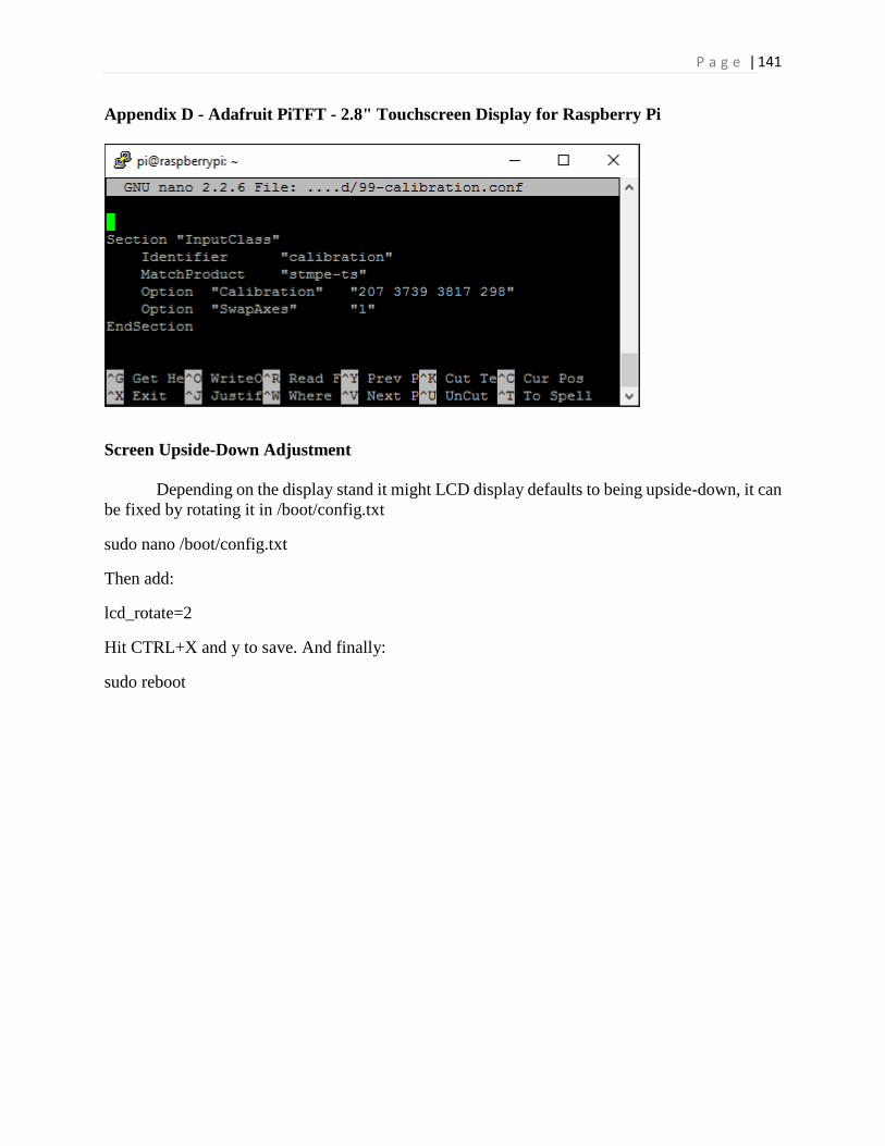
P a g e |
141
Appendix D - Adafruit PiTFT - 2.8" Touchscreen Display for Raspberry Pi
Screen Upside-Down Adjustment
Depending on the display stand it might LCD display defaults to being upside-down, it can
be fixed by rotating it in /boot/config.txt
sudo nano /boot/config.txt
Then add:
lcd_rotate=2
Hit CTRL+X and y to save. And finally:
sudo reboot

P a g e |
142
Appendix E - RaspiCam
The RaspiCam is a critical component of this thesis project. With a Raspberry Pi Camera,
it will greatly improve the frame rate. Additionally, if a Webcam were used, we would have to
find one that is small enough to be wearable. The following link is the official location for the
RaspiCam:
http://www.uco.es/investiga/grupos/ava/node/40
There is limited documentation for this library. We have to resort to reading the source code as the
documentation.
Official location of the RaspiCam:
Download the file to your raspberry. Then, decompress the file and compile
wget https://sourceforge.net/projects/raspicam/files/latest/download/raspicam.zip
unzip raspicam.zip
rm raspicam.zip
cd raspicam-0.1.3
mkdir build
cd build
cmake ..