Design and Implementation of a Micro-Inverter for ...
125
Munster Technological University Munster Technological University SWORD - South West Open Research SWORD - South West Open Research Deposit Deposit Masters Engineering 1-1-2018 Design and Implementation of a Micro-Inverter for Photovoltaic Design and Implementation of a Micro-Inverter for Photovoltaic Applications Applications Chi-Thang Phan-Tan Cork Institute of Technology Follow this and additional works at: https://sword.cit.ie/engmas Part of the Electrical and Electronics Commons Recommended Citation Recommended Citation Phan-Tan, Chi-Thang, "Design and Implementation of a Micro-Inverter for Photovoltaic Applications" (2018). Masters [online]. Available at: https://sword.cit.ie/engmas/2 This Thesis is brought to you for free and open access by the Engineering at SWORD - South West Open Research Deposit. It has been accepted for inclusion in Masters by an authorized administrator of SWORD - South West Open Research Deposit. For more information, please contact [email protected].
Transcript of Design and Implementation of a Micro-Inverter for ...

Munster Technological University Munster Technological University
SWORD - South West Open Research SWORD - South West Open Research
Deposit Deposit
Masters Engineering
1-1-2018
Design and Implementation of a Micro-Inverter for Photovoltaic Design and Implementation of a Micro-Inverter for Photovoltaic
Applications Applications
Chi-Thang Phan-Tan Cork Institute of Technology
Follow this and additional works at: https://sword.cit.ie/engmas
Part of the Electrical and Electronics Commons
Recommended Citation Recommended Citation Phan-Tan, Chi-Thang, "Design and Implementation of a Micro-Inverter for Photovoltaic Applications" (2018). Masters [online]. Available at: https://sword.cit.ie/engmas/2
This Thesis is brought to you for free and open access by the Engineering at SWORD - South West Open Research Deposit. It has been accepted for inclusion in Masters by an authorized administrator of SWORD - South West Open Research Deposit. For more information, please contact [email protected].

DESIGN AND IMPLEMENTATION OF A MICRO-INVERTER
FOR PHOTOVOLTAIC APPLICATIONS
CHI-THANG PHAN-TAN

DESIGN AND IMPLEMENTATION OF A MICRO-INVERTER
FOR PHOTOVOLTAIC APPLICATIONS
CHI-THANG PHAN-TAN
Department of Electrical Engineering
Cork Institute of Technology
Submitted in fulfillment of the degree of
Master of Engineering by Research in Electrical Engineering
Supervisors:
Joe Connell
Martin Hill
Noel Barry
Cork Institute of Technology, November, 2017

ACKNOWLEDGEMENTS
I would like to appreciate to my supervisors for assisting me to finish this hard project.
Firstly, I am very thankful to Prof. Noel Barry who has supported me from the beginning
when I was lonely and everything was strange to me. Through many conversations with you,
I gained confidence and the courage to keep moving forward. Then, I would like to thank Dr.
Martin Hill who gave me valuable comments and ideas for the thesis. He was busy but he
still spent time to talk and gave advice for my problems. I also want to express appreciation
to Dr. Nam Nguyen-Quang who has built a strong foundation for me in the electrical field,
especially the photovoltaic inverters. He has advised and inspired me in practical approach
such as designing the hardware circuit and microcontroller programming. As well, I wish to
acknowledge Dr. Joe Connell who is my main supervisor and he has supported me in general
to guarantee the successful completion of my thesis.
I am really grateful to Cork Institute of Technology where I can find support from many kind
people. I would like to say thank you to Mrs. Orla Flynn and Mr. An Phan who gave me the
opportunity to study in this lovely institute. I also want to thank Pio, Geraldine, Andrea,
Carmel, Niamh and Alan who helped and assisted me in the new environment and paper
works. Pertaining to electrical supports, I am thankful to Gary, Kevin and Liam who helped
me in designing and building the hardware circuit.

DECLARATION
I hereby declare that this submission is my own work and that, to the best of my knowledge
and belief, it contains no material previously published or written by another person nor
material to a substantial extent has been accepted for the award of any other degree or
diploma by a university of higher learning, except where due acknowledge has been made in
the text.
Signature of author: …………………………………..
Certified by: …………………………………..
Date: …………………………………..

ABSTRACT
The objective of this work is to design and build a novel topology of a micro-inverter to
directly convert DC power from a photovoltaic module to AC power. In the proposed micro-
inverter, a structure with two power stages, which are DC/DC and then DC/AC converters, is
used. The inverter is designed capable for future integration of battery as a buffer in between
the DC/DC and DC/AC converters.
A novel MPPT algorithm is implemented and evaluated in the DC/DC converter to optimize
the solar panel energy production. The new method operates with an efficiency of 99.23%,
which is a 2.5% improvement on the standard method, and a response time of less than 0.2s.
A modification of designing the inductor and transformer using Litz wires is also mentioned.
The core using Litz wires may reduce the Eddy current effect and is 15% smaller than the
coil using a single conductor.
In this research, the following approach is taken. A literature review was conducted, to
identify potential converter topologies. A topology for both converters was selected by
comparison of performance through simulations. Maximum Power Point Tracking
algorithms were also investigated, to select an appropriate control scheme. A design for two
converters was then performed, leading to a prototype for experimental verification.

TABLE OF CONTENT
CHAPTER 1. INTRODUCTION ................................................................................... 1
1.1. Micro-inverter ....................................................................................................... 1
1.1.1. Introduction ............................................................................................... 1
1.1.2. Topology ................................................................................................... 2
1.2. Research Context and Contribution to the Research Field ................................. 4
1.3. Research methodology .......................................................................................... 5
CHAPTER 2. STATE OF THE ART ............................................................................ 6
2.1. DC/DC converter ................................................................................................... 6
2.2. MPPT algorithms .................................................................................................. 8
2.2.1. Perturb and Observe method ...................................................................... 9
2.2.2. Incremental Conductance method ............................................................ 11
2.3. Micro-inverter topology ...................................................................................... 12
2.4. Distribution code and grid-connection requirements ........................................ 16
2.4.1. Grid standard ........................................................................................... 16
2.4.2. Grid-connection requirements .................................................................. 18
CHAPTER 3. DC/DC CIRCUIT DESIGN .................................................................. 20
3.1. Theory .................................................................................................................. 20
3.1.1. DC/DC converter ..................................................................................... 20
3.1.2. MPPT algorithm ...................................................................................... 28
3.1.2.1. Modified Perturb & Observe method ........................................ 28
3.1.2.2. Binary-search-based Perturb & Observe method ...................... 30
3.2. Refinement of MPPT algorithms ........................................................................ 32
3.3. Simulation ............................................................................................................ 35
3.4. Circuit board design ............................................................................................ 39
3.4.1. Power Supply .......................................................................................... 40
3.4.2. MOSFET gate driver ............................................................................... 41
3.4.3. Current sensor ......................................................................................... 42
3.4.4. Voltage sensor ......................................................................................... 43
3.4.5. Inductor and capacitor conditions ............................................................ 44
3.4.6. Inductor design ........................................................................................ 45
3.4.6.1. Methodology ............................................................................. 45
3.4.6.2. Calculation for the inductor ...................................................... 50
3.5. Programming....................................................................................................... 54
3.6. Experimental results ........................................................................................... 56

3.6.1. SEPIC circuit ........................................................................................... 56
3.6.2. MPPT test ................................................................................................ 60
3.6.2.1. Efficiency test ........................................................................... 62
3.6.2.2. Response test ............................................................................ 66
CHAPTER 4. DC/AC CIRCUIT DESIGN .................................................................. 68
4.1. Theory .................................................................................................................. 68
4.1.1. Power topology........................................................................................ 68
4.1.2. Power control theory................................................................................ 73
4.2. Simulation ............................................................................................................ 75
4.3. Circuit board design ............................................................................................ 78
4.3.1. Transformer design .................................................................................. 79
4.3.1.1. Methodology ............................................................................. 79
4.3.1.2. Calculation for the transformer ................................................ 81
4.3.2. Grid measuring ........................................................................................ 83
4.3.2.1. Grid filtering ............................................................................ 84
4.3.2.2. Grid zero-crossing detector ...................................................... 85
4.3.2.3. Grid peak detector .................................................................... 85
4.3.3. MOSFET gate driver ............................................................................... 86
4.4. Programming....................................................................................................... 87
4.4.1. SPWM generating ................................................................................... 87
4.4.2. Frequency control .................................................................................... 88
4.4.3. Phase control ........................................................................................... 88
4.4.4. Operation ................................................................................................. 88
4.5. Experimental results ........................................................................................... 90
4.5.1. Grid measuring ........................................................................................ 91
4.5.1.1. Grid filtering ............................................................................ 91
4.5.1.2. Grid zero-crossing detector ...................................................... 92
4.5.1.3. Grid peak detector .................................................................... 92
4.5.2. DC/AC circuit ......................................................................................... 93
CHAPTER 5. CONCLUSION ..................................................................................... 96
5.1. Achievements ....................................................................................................... 96
5.2. Problems and future work .................................................................................. 97

LIST OF FIGURES
Figure 1.1: Power density vs. energy density of various energy storage systems [14] ............ 2
Figure 1.2: Two-stage PV inverter topologies ....................................................................... 3
Figure 1.3: The block diagram of the micro-inverter ............................................................. 4
Figure 2.1: Isolating DC/DC converter topologies [15] ......................................................... 6
Figure 2.2: Non-isolating DC/DC converter topologies [15][16] ........................................... 7
Figure 2.3: Typical PV Current-Voltage & Power-Voltage Curves [17] ................................ 8
Figure 2.4: Flowchart of traditional Perturb & Observe method ............................................ 9
Figure 2.5: Illustration of P&O with small step ................................................................... 10
Figure 2.6: Illustration of P&O with large step ................................................................... 11
Figure 2.7: Flowchart of traditional Incremental Conductance method ............................... 12
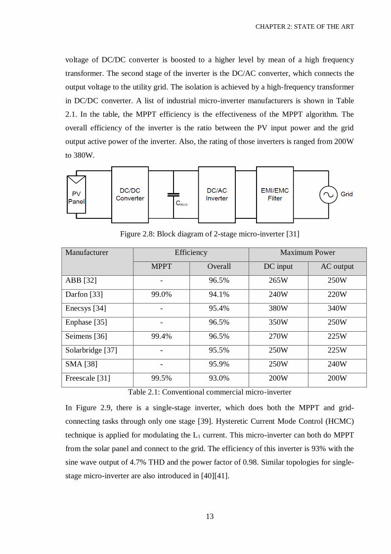
Figure 2.8: Block diagram of 2-stage micro-inverter [31] ................................................... 13
Figure 2.9: Single-stage micro-inverter [39] ....................................................................... 14
Figure 2.10: Boost half-bridge micro-inverter [42] ............................................................. 14
Figure 2.11: Topology of CIDBI [44] ................................................................................. 14
Figure 2.12: MEB micro-inverter [45] ................................................................................ 15
Figure 2.13: H-bridge LLC topology [46] ........................................................................... 15
Figure 2.14: Single-stage Isolated High-frequency link Series Resonant Inverter [47] ........ 16
Figure 3.1: Schematic of SEPIC circuit .............................................................................. 21
Figure 3.3: Voltage waveforms of components of SEPIC circuit......................................... 26
Figure 3.4: Current waveforms of components of SEPIC circuit ......................................... 27
Figure 3.2: Relation of SEPIC input voltage and current with output resistor ...................... 28
Figure 3.5: Flowchart of Modified P&O method ................................................................ 29
Figure 3.6: Flowchart of BS-P&O method .......................................................................... 30
Figure 3.7: Illustration of BS-P&O method ........................................................................ 31
Figure 3.8: Flowchart of Modified P&O in simulation and programming ........................... 32
Figure 3.9: Flowchart of INC in simulation and programming ............................................ 33
Figure 3.10: Flowchart of BS-P&O in simulation and programming ................................... 34
Figure 3.11: MATLAB simulation model for MPPT verification ........................................ 35
Figure 3.12: Modified P&O and INC simulation results ..................................................... 36
Figure 3.13: Binary-Search-Based P&O simulation results ................................................. 37
Figure 3.14: Solar module of the experiment ...................................................................... 39
Figure 3.15: Laboratory prototype of DC/DC board............................................................ 40
Figure 3.16: Schematic of 5V and 12V power supplies ....................................................... 41

Figure 3.17: Schematic of low-side MOSFET driver .......................................................... 42
Figure 3.18: Current transducer LTS 6-NP ......................................................................... 42
Figure 3.19: Schematic of DC voltage sensor ..................................................................... 43
Figure 3.20: Basic E-core inductor ..................................................................................... 45
Figure 3.21: Litz wire ......................................................................................................... 46
Figure 3.22: Implemented inductors ................................................................................... 53
Figure 3.23: Measurement of the inductor .......................................................................... 54
Figure 3.24: Pin diagram of TM4C123G LaunchPad Evaluation Board [57] ....................... 54
Figure 3.25: Tiva C Series TM4C123G LaunchPad Evaluation Board [58] ......................... 55
Figure 3.26: Example of ADC 4-sample averaging of sequencer SS0 ................................. 56
Figure 3.27: Experimental SEPIC circuit for performance testing ....................................... 57
Figure 3.28: Experiment result of SEPIC input and output voltages .................................... 57
Figure 3.29: Experiment and simulation results of SEPIC 𝐶1 voltage ................................. 58
Figure 3.30: Experiment and simulation results of SEPIC 𝐿1 voltage ................................. 58
Figure 3.31: Experiment and simulation results of SEPIC 𝐿2 voltage ................................. 59
Figure 3.32: Experiment and simulation results of SEPIC switch voltage ........................... 59
Figure 3.33: Experiment and simulation results of SEPIC diode voltage ............................. 60
Figure 3.34: MPPT testing set-up ....................................................................................... 60
Figure 3.35: Block connection of the MPPT testing ............................................................ 61
Figure 3.36: Output resistors for MPPT testing ................................................................... 61
Figure 3.37: Pyranometer SP Lite2 ..................................................................................... 62
Figure 3.38: PV Current-Voltage curve of different temperatures [61] ................................ 62
Figure 3.39: Temperature sensor location for the experiment .............................................. 63
Figure 3.40: Experiment and simulation results of modified P&O ...................................... 64
Figure 3.41: Experiment and simulation results of BS-P&O ............................................... 65
Figure 3.42: Experiment results of modified P&O response ................................................ 66
Figure 3.43: Experiment results of BS-P&O response......................................................... 67
Figure 4.1: Inverter output waveform before filtering at 4kHz (Illustration) ........................ 69
Figure 4.2: FFT analysis of the inverter waveform before filtering at 40kHz in 0.1s ........... 69
Figure 4.3: Waveform to pass through transformer at 4kHz (Illustration) ............................ 70
Figure 4.4: FFT analysis of waveform used for transformer at 40kHz in 0.1s ...................... 70
Figure 4.5: Schematic of DC/AC circuit ............................................................................. 71
Figure 4.6: Output voltage of transformer ........................................................................... 72
Figure 4.7: Output voltage of rectifier ................................................................................. 72
Figure 4.8: Output voltage of polar reverse bridge .............................................................. 72

Figure 4.9: Output voltage of filter ..................................................................................... 73
Figure 4.10: Power transfer model ...................................................................................... 73
Figure 4.11: Phasor diagram between grid and inverter voltage .......................................... 74
Figure 4.12: MATLAB simulation model DC/AC converter ............................................... 75
Figure 4.13: Simulated output voltage and current of polar reverse bridge .......................... 76
Figure 4.14: Simulated output voltage and current of filter ................................................. 76
Figure 4.15: Simulated output active power and reactive power of inverter......................... 77
Figure 4.16: Inverter amplitude and phase angle versus output power ................................. 77
Figure 4.17: Laboratory prototype of DC/AC board............................................................ 78
Figure 4.18: Basic E-core 2-coil transformer ...................................................................... 79
Figure 4.19: Laboratory prototype of grid sensing board ..................................................... 83
Figure 4.20: ICL7660 circuit of -5V supply ........................................................................ 83
Figure 4.21: Schematic circuit of 2nd-order Sallen-Key Low-pass-filter [62] ....................... 84
Figure 4.22: Bode diagram of the active filter ..................................................................... 84
Figure 4.23: Schematic circuit of ZCD ............................................................................... 85
Figure 4.24: Schematic circuit of peak detector .................................................................. 85
Figure 4.25: Schematic of high-side MOSFET driver ......................................................... 86
Figure 4.26: Schematic of isolated 5V&12V supplies for MOSFET driver ......................... 86
Figure 4.27: Example of 50Hz sine values with sampling of 4kHz...................................... 87
Figure 4.28: ZCD signal and grid voltage ........................................................................... 88
Figure 4.29: Simple flowchart of inverter programming ..................................................... 89
Figure 4.30: Block connection of the experiment ................................................................ 90
Figure 4.31: Grid voltage and grid filtered signal ................................................................ 91
Figure 4.32: Zero-crossing detector output and grid filtered signal...................................... 92
Figure 4.33: Peak detector output and grid filtered signal ................................................... 93
Figure 4.34: Experimental result of transformer output voltage ........................................... 94
Figure 4.35: Experimental result of the inverter output ....................................................... 94

LIST OF TABLES
Table 2.1: Conventional commercial micro-inverter ........................................................... 13
Table 2.2: Harmonic voltage distortion for individual orders .............................................. 17
Table 3.1: Average voltage and current values of SEPIC components................................. 25
Table 3.2: Simulation values for SEPIC components .......................................................... 35
Table 3.3: Simulation values for MPPT parameters ............................................................ 35
Table 3.4: Comparison of MPPT methods .......................................................................... 38
Table 3.5: Technical information of PLM-280M-72 solar module ...................................... 39
Table 3.6: Values of the air gap correction.......................................................................... 50
Table 3.7: Initial values for calculating inductor ................................................................. 51
Table 3.8: Specifications of ferrite core ETD49 [56] ........................................................... 51
Table 3.9: Experimental efficiency comparison of MPPT methods ..................................... 65
Table 4.1: Simulation values for inverter parameters .......................................................... 75
Table 4.2: Initial values for calculating transformer ............................................................ 82

ACRONYMS
AC Alternative Current
ADC Analog to Digital Converter
BS-P&O Binary-Search-Based Perturb and Observe method
BST Bisection search theorem
CCC Charge Control Circuit
CCS Code Composer Studio (integrated development environment)
CIDBI Couple-inductor double-boost inverter
DC Direct Current
FFT Fast Fourier Transform
HCMC Hysteretic Current Mode Control
HF High-Frequency
HV High Voltage
ICDI In-circuit Debug Interface
INC Incremental Conduction method
LC filter Filter which has an inductor (L) and a capacitor (C) connected to each other
LPF Low-pass filter
LV Low Voltage
MEB Multilevel Energy Buffer
MOSFET Metal-Oxide Semiconductor Field-Effect Transistor
MPP Maximum Power Point
MPPT Maximum Power Point Tracking
MLT Mean Length of a Turn of winding wires
Op-amp Operational Amplifier
P&O Perturb and Observe method
PCB Printed Circuit Board
PV Photovoltaic
PWM Pule-Width-Modulation
RMS Root-Mean-Square value
SCEB Switched-Capacitor Energy Buffer
SEPIC Single-Ended Primary-Inductor Converter
SPWM Sinusoidal Pule-Width-Modulation
STC Standard Test Condition
THD Total Harmonic Distortion
ZCD Zero-crossing Detector

NOMENCLATURE
INDUCTOR and TRANSFORMER DESIGNING SECTION
Label Description Unit
𝐴𝑐 cross-sectional area of the core m2
𝐴𝐿 induction factor H
𝐴𝐿𝑖𝑡𝑧 overall cross-sectional area of a Litz wire m2
𝐴𝑝 product of 𝐴𝑐 and 𝐴𝑤𝑑 m4
𝐴𝑠𝑡𝑎𝑛𝑑 strand wire area m2
𝐴𝑠𝑡𝑎𝑛𝑑_𝑝 strand wire area of primary side of transformer m2
𝐴𝑠𝑡𝑎𝑛𝑑_𝑠 strand wire area of secondary side of transformer m2
𝐴𝑡 surface area of core m2
𝐴𝑤 overall cross-sectional area of the winding m2
𝐴𝑤𝑑 window area of core for winding m2
𝐵𝑚𝑎𝑥 maximum flux density (typical 𝐵𝑚𝑎𝑥 ≈ (0.6 − 0.7)𝐵𝑠𝑎𝑡) T
𝐵𝑜 optimum flux density of transformer T
𝐵𝑠𝑎𝑡 saturation flux density T
∆𝐵 flux density ripple T
𝑑𝑠𝑡𝑎𝑛𝑑 strand wire diameter m
𝑓 frequency of current Hz
𝑁 number of turns of inductor 1
𝑁𝑝 number of primary turns of transformer 1
𝑁𝑠 number of secondary turns of transformer 1
𝑛𝐿𝑖𝑡𝑧 number of Litz wires of inductor 1
𝑛𝐿𝑖𝑡𝑧_𝑝 number of Litz wires of primary side of transformer 1
𝑛𝐿𝑖𝑡𝑧_𝑠 number of Litz wires of secondary side of transformer 1
ℎ𝑐 heat transfer coefficient (typical ℎ𝑐 = 10) W/m2 °C
𝐼𝐿_𝑚𝑎𝑥 maximum current of inductor A
𝐼𝐿_𝑟𝑚𝑠 RMS of inductor current A
𝐼𝑟𝑚𝑠_𝑝 RMS current of primary side of transformer A
𝐼𝑟𝑚𝑠_𝑠 RMS current of secondary side of transformer A
𝐽0 current density A/m2
𝑘𝑎 coefficient; 𝑘𝑎 = 𝐴𝑡/𝐴𝑝1/2
(typical 𝑘𝑎 = 40) 1
𝑘𝑐 coefficient; 𝑘𝑐 = 𝑉𝑐/𝐴𝑝3/4
(typical 𝑘𝑐 = 5.6) 1
𝑘𝑐𝑜𝑟𝑒 material parameter (N87 material 𝑘𝑐 = 16.9) 1
𝑘𝑖 current coefficient; 𝑘𝑖 = 𝐼𝐿_𝑟𝑚𝑠/𝐼𝐿_𝑚𝑎𝑥 1
𝑘𝑔 air gap correction coefficient 1
𝑘𝑡 coefficient (typical 𝑘𝑡 = 48.2 × 10³) (A2/m3 °C)1/2
𝑘𝑢 window utilization factor; 𝑘𝑢 = 𝐴𝑤/𝐴𝑤𝑑 1

𝑘𝑣 waveform factor 1
𝑘𝑤 coefficient; 𝑘𝑤 = 𝑉𝑤/𝐴𝑝3/4
(typical 𝑘𝑤 = 10) 1
𝐿 needed inductance H
𝑙𝑐 effective magnetic path length M
𝑙𝑔 length of the air gap M
𝑙𝑡𝑢𝑟𝑛 mean length of a turn (MLT) of winding wires M
𝑃𝑐𝑜𝑟𝑒 power loss of the core W
𝑃𝐷 maximum dissipation power of the core W
𝑃𝑖𝑛 input power of transformer W
𝑃𝑙𝑜𝑠𝑠 total power loss of the inductor; 𝑃𝑙𝑜𝑠𝑠 = 𝑃𝑐𝑜𝑟𝑒 + 𝑃𝑤𝑖𝑟𝑒 W
𝑃𝑤𝑖𝑟𝑒 power loss of the winding wire W
𝑅𝑤𝑖𝑟𝑒 resistance of the copper winding wire Ω
𝑅𝑤𝑖𝑟𝑒_𝑝 resistance of the copper winding wire in primary side Ω
𝑅𝑤𝑖𝑟𝑒_𝑠 resistance of the copper winding wire in secondary side Ω
𝑅𝜃 thermal resistance of the core °C/W
ℛ𝑒𝑞 equivalent magnetic reluctance 1/H
ℛ𝑐 magnetic reluctance of the core 1/H
ℛ𝑔 magnetic reluctance of the air gap 1/H
𝑇 Temperature °C
𝑇𝑚𝑎𝑥 maximum temperature; 𝑇𝑚𝑎𝑥 = 𝑇 + ∆𝑇 °C
∆𝑇 temperature rise °C
𝑉𝑐 volume of the core m3
𝑉𝑟𝑚𝑠_𝑝 RMS voltage of primary side of transformer V
𝑉𝑤 volume of the winding m3
𝛼 material parameter (N87 material 𝛼 = 1.25) 1
𝛼0 temperature coeff. of resistivity at 20°C (𝛼0_𝑐𝑢 = 0.004) 1/°C
𝛽 material parameter (N87 material 𝛽 = 2.35) 1
𝛾 coefficient; 𝛾 = 𝑃𝑐𝑜𝑟𝑒/𝑃𝑤𝑖𝑟𝑒 1
𝛿 skin depth M
𝜇0 magnetic permeability of free space; 𝜇0 = 4𝜋 × 10−7 H/m
𝜇𝑟 relative permeability 1
𝜇𝑒 effective relative permeability 1
𝜇𝑒_𝑜𝑝𝑡 optimum effective relative permeability 1
𝜌 resistivity of conductor Ωm
𝜌0 resistivity of conductor at 20°C (𝜌0_𝑐𝑢 = 1.72 × 10⁻⁸) Ωm

CHAPTER 1: INTRODUCTION
1
CHAPTER 1. INTRODUCTION
In this section, the motivation to select the research topic is presented. The potential
contributions of this research are outlined and the method of conducting the research is
also shown.
1.1. Micro-inverter
1.1.1. Introduction
Energy sources are amongst the most important challenges facing both the world’s
industrialized and developing countries. The amount of fossil fuel is now decreasing and
this kind of energy causes a lot of environmental problems. Renewable or green energy is
therefore being developed at high speed recently, especially solar energy. One of methods
to harvest the solar energy is using the photovoltaic (PV) modules, which absorb the sun’s
photonic energy and transfer it to electricity with a p-n junction. In comparison to other
kinds of renewable energy systems, there is no moving part in a solar system, which means
that the solar systems may last for a long time with minimum maintenance [1].
In PV systems, inverters are used for converting DC from a solar panel to AC to connect
directly to the utility grid. Inverters used in PV applications in the market are mainly
configured in central and string formats with the power ratings above 5kW. Residential PV
projects are increasing because of the steadily decreasing prices of solar installations and
devices [2]. This requires other kinds of inverter with low power rating. Micro-inverters
are designed for use of low power input. The micro-inverter converts DC to AC and
connects to the grid from a solar module whose maximum power rating is about 350W.
Micro-inverters have many advantages in comparison with string-inverters [3]. As reported
in [4], micro-inverters supply 11.36% higher energy output than string-inverters in the case
of partial shading. In clear sky condition, micro-inverters produce 20% more power than
string inverters [5]. Inverters are the most unreliable components in solar systems [6], and
the micro-inverters should be more desirable than string-inverters with failure rates are
lower than that of string-inverters [1]. Moreover, according to [1] the cost of installing a
system, including equipment, maintenance and labor, using string-inverters is higher than
that of a system with micro-inverters. Another aspect to be considered is safety, where
high DC voltage is the likely cause of arc faults and can also sustain arcs better than AC

CHAPTER 1: INTRODUCTION
2
voltage [7][8]. Since the operating DC voltage of micro-inverters is much lower than
string-inverters, the micro-inverter should lower the risk of arc faults or system fires [1][9].
In comparison to string-inverters, micro-inverters are simpler, as they deal with a lower
power range [10]. In addition, the flexibility of PV systems could be increased by avoiding
connecting several solar modules into strings.
1.1.2. Topology
The purpose of this research is to design a micro-inverter which can integrate a small
battery. The reasons for designing a topology which is capable for a battery to be a buffer
are introduced as the following. First, in comparison to capacitors, the capacity of a battery
is higher. As seen in Figure 1.1, the batteries have larger energy density than capacitors,
this means in the same size and weight, the batteries can store larger amount of energy than
the capacitors. Second, the batteries can also be used as a power supply for the control
circuit at night while there is no power from the sun. Third, the batteries can balance the
input and output of the inverter by storing or supplying energy. These features of batteries
can be used for smart inverters in micro-grid and smart-grid applications [11][12][13].
Figure 1.1: Power density vs. energy density of various energy storage systems [14]
The design difference between the string inverter and micro-inverter is the DC input
voltage. As seen in Figure 1.2(a), the input of string inverter is an array of PV panels. The
input of the inverter is usually up to 600V, the inverter does not need to increase the
voltage to grid level, therefore the DC/DC and DC/AC topologies are simple. For instance,
the DC/AC circuit is just a H-bridge of four switches.

CHAPTER 1: INTRODUCTION
3
The input of a micro-inverter is around 30V while its output is over 350V-peak. Therefore,
a transformer is needed to boost low input voltage to grid level. The common topology of
micro-inverter is shown in Figure 1.2(b). The low input voltage is boosted to high DC
voltage by a DC/DC converter integrated with a high-frequency transformer (typical
topologies of this DC/DC converter are presented in Figure 2.1). The DC buffer is usually
made of capacitors of high-voltage rating.
Figure 1.2: Two-stage PV inverter topologies
(a) String inverter (b) Micro-inverter with capacitor buffer
(c) Micro-inverter with battery buffer and low-frequency transformer
(d) Micro-inverter with battery buffer and high-frequency transformer
As mentioned, the goal of this research is to integrate a battery. However, the battery
voltage is low, for example a Li-ion cell is 3.7V, so that to make higher voltage, several
cells are connected in series. By putting the battery in the DC-link, the topology of micro-
inverter is presented in Figure 1.2(c). The micro-inverter has similar topology to the two-
stage string inverter. After the DC/AC converter, the 50Hz low voltage AC will pass
through a transformer to boost the voltage to grid level. However, it is known that the

CHAPTER 1: INTRODUCTION
4
lower the frequency, the larger the transformer. Hence, the 50Hz transformer is large in
comparison to the size of the inverter.
Another approach is shown in Figure 1.2(d). The power flow is similar to the topology in
Figure 1.2(c), but in the DC/AC converter, a high-frequency transformer is integrated
making the size of the transformer small enough for a micro-inverter. The power flow
topology as shown in Figure 1.2(d) is adopted in this work.
1.2. Research Context and Contribution to the Research Field
The research is concerned about the design and construction of a micro-inverter, which
takes maximum power from a solar module and produces AC power at the output. The
research deals with the design of a power circuit and its control algorithms.
The power circuit composes of two parts, the DC/DC and the DC/AC converters. The
DC/DC converter is responsible for obtaining the maximum power from the solar module.
The DC/AC inverter produces AC power for the output load. The DC/DC converter should
have a continuous input current for efficient power extraction. A high quality output will
be needed for the inverter. For safety and compactness, a high frequency transformer is
also used. The diagram of the micro-inverter structure is shown in Figure 1.3.
Figure 1.3: The block diagram of the micro-inverter
Contributions of the research to the general field research are:
- Selection of topologies for DC/DC and DC/AC converters.
- Design inverter topology which is able to integrate the battery as a buffer in between the
DC/DC and DC/AC converter.
- A novel Maximum Power Point Tracking (MPPT) algorithm.
- Design inductors and transformer using Litz wires
The design of this inverter contributes a new control algorithm of MPPT for the PV
applications. It also introduces a different type of DC/AC power circuit in which the high-

CHAPTER 1: INTRODUCTION
5
frequency transformer is applied with pule-width-modulation (PWM) waveform. In
addition, it is the introduction for the inverter topology which is able to have a battery
application in the future. Note that, the control of optimizing the use of the battery is
beyond the scope of this thesis. The battery will be investigated later in other work. In this
thesis, the topology of the DC/DC and DC/AC is the focus.
1.3. Research methodology
The methodology of this research is laboratory work consisting of experiment and
simulation. The first task is literature review, which includes identifying suitable power
topologies and control algorithms for the micro-inverter. It was made by reviewing papers
from academic conferences and journals. After selecting the potential circuits and
algorithms, simulations were conducted using MATLAB software. The final power and
control schemes were chosen by comparing simulated performance and suitability. A
hardware power circuit was built for experimental verification. Power components and
measuring equipment were required for this task.
The micro-inverter is the combination of the DC/DC and the DC/AC converters.
Therefore, this thesis is divided into two main parts which are DC/DC and DC/AC circuit
designs. In Chapter 2, the review of topologies of the converters and the MPPT methods is
introduced. The review is the basis for selecting the suitable converter topologies for the
micro-inverter. Chapter 3 describes the design of the DC/DC converter from theory,
simulation, implementation, programming to the experiment. One of the main parts of this
chapter is the introduction of a novel MPPT algorithm which is based on the binary-
searching method. This MPPT method is verified in the simulation and the experiment for
a better performance in comparison to the conventional MPPT methods. The introduction
of the inductor design using Litz wires is also described in detail. In Chapter 4, the DC/AC
topology is presented. The DC/AC topology is analyzed and simulated for its operation.
The sensor circuits for measuring the grid are also introduced in this chapter. The
methodology in the programming and control of the microcontroller is described. Similar
to the inductor design, the detailed development of a high frequency transformer design is
presented in this chapter. The conclusion in Chapter 5 summarizes the achievements of the
project and problems encountered in the design process. Also, the detailed code for the
microcontroller is shown in the Appendix.

CHAPTER 2: STATE OF THE ART
6
CHAPTER 2. STATE OF THE ART
In this section, the conventional topologies of DC/DC and DC/AC converters used for PV
applications are presented. A review of algorithms for tracking the maximum power point
(MPP) of a solar module is also presented. Finally, the state of the art for micro-inverter
technology is reviewed and the main topologies and their characteristics are outlined.
2.1. DC/DC converter
There are many types of DC/DC converter, which are suitable for the PV applications. The
main duty of the DC/DC converter is to track the MPP of PV panels. It does so by
increasing or decreasing the duty cycle of one or several active switches.
Figure 2.1: Isolating DC/DC converter topologies [15]
There are two main types of DC/DC converter. The first type is isolating converters with
high-frequency transformers for isolation. The input and output of the converter are

CHAPTER 2: STATE OF THE ART
7
electrically isolated by the transformer because the input and output are using separated
ground connection. Moreover, the transformer has a function of boosting the low level
input voltage to a higher level. There are many topologies for this kind of converter such as
fly-back, push-pull, forward, half-bridge and full-bridge [15].
The isolating converter has the transformer which acts as an isolating component. In the
isolating converter, the direct current is transformed to AC to pass through the transformer.
After that, the power is rectified and a typical LC filter at the output takes the
responsibility of filtering high frequency components. In addition, its output is at high
voltage level, which helps the following DC/AC circuit to be designed smaller. However,
the purpose of this project is to apply the battery buffer in between the DC/DC and DC/AC
converters, so that the output of the converter should be low level and defined by the
battery.
The second type of DC/DC converter is non-isolating converters. This type does not
include a transformer so that it does not have magnetic and electrical isolation. Figure 2.2
shows the topologies of buck-boost DC/DC converters, which are able to make the output
voltage lower or higher relative to the input voltage. Four typical topologies are buck-
boost, Cuk, continuous input current buck-boost and SEPIC [15] [16].
Figure 2.2: Non-isolating DC/DC converter topologies [15][16]
One compulsory requirement is that the output current of the PV, or the input current of the
DC/DC converter, must be continuous. The continuous mode means that the input current
of the converter will never go down to zero during the operation. In the case of
discontinuous input current mode, the output current of PV panel is interrupted or goes
down to zero which leads to the failure of getting maximum power. The buck-boost

CHAPTER 2: STATE OF THE ART
8
converter has a switch in the input which means the input current would be interrupted or
equal to zero when the switch is turned off. The buck-boost converter does not meet the
continuous input current condition so that it is not chosen. The remaining three converters
fulfill the requirement of continuous input current and they can buck or boost the input
voltage as required by this project. However, output voltages of Cuk and continuous input
current buck-boost converters are inversed with respect to the input voltages, leading to
some difficulties in implementation. Therefore, we finally chose the SEPIC as the DC/DC
converter for this application.
2.2. MPPT algorithms
In Figure 2.3, the typical characteristic I-V and P-V curves are shown at different
irradiation values. It can be seen that with the higher irradiant, more power can be
harvested from the solar panel. However, the operating power point may be anywhere in
the P-V curve and it depends on the operating voltage of the panel. The energy of the solar
panel should be converted as much as possible when it is available, and this can be done by
applying MPPT algorithms. These methods are used to control the DC/DC converters to
dynamically adapt its operating point to the MPP of the PV.
Figure 2.3: Typical PV Current-Voltage & Power-Voltage Curves [17]
There are many algorithms for finding the MPP of solar panels. Some methods are simple
and easy to control such as: Fractional Open-Circuit Voltage VOC [18], Fractional Short-
Circuit Current ISC [19], Perturb-and-Observe (P&O) [20][21][22] and the Incremental

CHAPTER 2: STATE OF THE ART
9
Conductance (INC) [23][24][25]. However, there are complex methods for doing the task
of tracking MPP [26][27] such as Current Sweep [28], Fuzzy Logic Control [29] and
Artificial Neural Network [30]. These complex methods require a lot of calculations and
memory, implying the need to use more powerful microcontrollers due to heavier
computational load than that of simple methods. Hence, this project focuses on simple and
effective MPPT method. The following is the detail explanation of two common MPPT
algorithms P&O and INC, which will be mentioned on the later section.
2.2.1. Perturb and Observe method
One of the most popular ways of MPPT is the P&O method, with flowchart being shown
in Figure 2.4.
Figure 2.4: Flowchart of traditional Perturb & Observe method
The P&O is a straightforward, simple and fairly effective algorithm. In the initial state, the
PV voltage V1 and I1 is measured. Then the voltage is changed by an amount of δV0. The
algorithm compares the previous power value to the current one. If there is difference, the
controller will adjust the voltage by an amount of δV0. The value of “k” is calculated to
make the decision of increasing or decreasing the voltage. When the operation power point

CHAPTER 2: STATE OF THE ART
10
is in the left of MPP, the value of “k” is positive and the voltage is increased to move
closer to the MPP. And when the power point is in the right of MPP, the value of k is
negative and the voltage is decreased. The efficiency of this algorithm depends on the
perturbation size δV0. The illustration is shown in Figure 2.5 and Figure 2.6 below.
Figure 2.5 shows the step δV0 in small value. The operation point is started in the left of
MPP and it takes many steps to reach the MPP.
Figure 2.5: Illustration of P&O with small step
In Figure 2.6, when δV0 is large, the algorithm can quickly move with large step but it
cannot to find the exact MPP and the perturbation is higher with the larger δV0.
In both cases of small and large δV0 values, the power point cannot get to the MPP and just
fluctuates around it. The second common MPPT algorithm is described in the next section.

CHAPTER 2: STATE OF THE ART
11
Figure 2.6: Illustration of P&O with large step
2.2.2. Incremental Conductance method
The second well-known algorithm of MPPT is the INC method. For this type of MPPT, the
slope dP/dV of the P-V curve is used as the control variable. The slope is equal to zero at
the MPP, positive on the left of MPP and negative on the right of MPP. The practical
algorithm makes use of the approximation below, avoiding power calculations and
derivations:
dP
dV=
d(VI)
dV= I + V
dI
dV≈ I + V
∆I
∆V (2.1)

CHAPTER 2: STATE OF THE ART
12
Then it can be concluded that:
{
dP/dV = 0dP/dV > 0dP/dV < 0
→ {
ΔI/ΔV = −I/V ΔI/ΔV > −I/V ΔI/ΔV < −I/V
at MPP
left of MPPright of MPP
(2.2)
This leads to the flowchart as shown in Figure 2.7.
Figure 2.7: Flowchart of traditional Incremental Conductance method
This method has an advantage of keeping the voltage from constantly fluctuate and
therefore can increase the overall efficiency. Similar to the P&O method, the INC method
depends on the value of δV0 or the perturbation of voltage is fixed to the values of δV0.
2.3. Micro-inverter topology
Micro-inverters are just widely applied and commercially used from 2005. However, there
are many topologies with advanced technologies and control, which are introduced in the
following.
The common topology of a micro-inverter of solar companies is shown in Figure 2.8. It is
a 2-stage system; the first stage is a DC/DC converter for getting the MPP. Then the output
CHAPTER 2: STATE OF THE ART
13
voltage of DC/DC converter is boosted to a higher level by mean of a high frequency
transformer. The second stage of the inverter is the DC/AC converter, which connects the
output voltage to the utility grid. The isolation is achieved by a high-frequency transformer
in DC/DC converter. A list of industrial micro-inverter manufacturers is shown in Table
2.1. In the table, the MPPT efficiency is the effectiveness of the MPPT algorithm. The
overall efficiency of the inverter is the ratio between the PV input power and the grid
output active power of the inverter. Also, the rating of those inverters is ranged from 200W
to 380W.
Figure 2.8: Block diagram of 2-stage micro-inverter [31]
Manufacturer Efficiency Maximum Power
MPPT Overall DC input AC output
ABB [32] - 96.5% 265W 250W
Darfon [33] 99.0% 94.1% 240W 220W
Enecsys [34] - 95.4% 380W 340W
Enphase [35] - 96.5% 350W 250W
Seimens [36] 99.4% 96.5% 270W 225W
Solarbridge [37] - 95.5% 250W 225W
SMA [38] - 95.9% 250W 240W
Freescale [31] 99.5% 93.0% 200W 200W
Table 2.1: Conventional commercial micro-inverter
In Figure 2.9, there is a single-stage inverter, which does both the MPPT and grid-
connecting tasks through only one stage [39]. Hysteretic Current Mode Control (HCMC)
technique is applied for modulating the L1 current. This micro-inverter can both do MPPT
from the solar panel and connect to the grid. The efficiency of this inverter is 93% with the
sine wave output of 4.7% THD and the power factor of 0.98. Similar topologies for single-
stage micro-inverter are also introduced in [40][41].

CHAPTER 2: STATE OF THE ART
14
Figure 2.9: Single-stage micro-inverter [39]
The 2-stage inverter is represented in Figure 2.10. In the first stage-DC/DC-a haft-bridge
of two switches is used for tracking the MPP. The efficiency of this topology is 98.2% at
the power input of 210W [42][43].
Figure 2.10: Boost half-bridge micro-inverter [42]
In Figure 2.11, the topology is the Couple-inductor double-boost inverter (CIDBI) [44]. It
uses four switches for generating a sine wave and connecting to the grid. A DC source B1
helps to increase the stability of the inverter. The experimental results for the power of
217.8W show the inverter’s efficiency of 97.5% and total harmonic content of less than
3%. However, there is no isolation between the inverter and the utility grid.
Figure 2.11: Topology of CIDBI [44]

CHAPTER 2: STATE OF THE ART
15
The next type of micro-inverter is represented in Figure 2.12 as the Multilevel Energy
Buffer (MEB) [45]. The MEB is connected in cascade between the input capacitor and a
DC/AC converter block. The MEB consists of a Switched-Capacitor Energy Buffer
(SCEB) and uses an optional Charge Control Circuit (CCC). The SCEB is used to
modulate the DC/AC converter block’s input voltage, functioning as an active energy
buffer to reduce the total energy storage requirement. The optional CCC provides an
additional means to balance the total charge entering and leaving the SCEB over a line
cycle. The DC/AC converter stage is operated above the resonant frequency to achieve
zero-voltage switching (ZVS) operation of 300kHz. This design can help the efficiency
improve to more than 98%.
Figure 2.12: MEB micro-inverter [45]
The topology in Figure 2.13 shows the full bridge LLC inverter [46]. Its overall efficiency
is 96% and it is able to provide reactive power to the grid.
Figure 2.13: H-bridge LLC topology [46]
The topology in Figure 2.14 is the series resonant inverter using soft-switching controlling
[47]. This micro-inverter comprises two active bridges, a series resonant tank and a high

CHAPTER 2: STATE OF THE ART
16
frequency transformer. This system can help by reducing the component quantity number
based on single-stage conversion. It also lowers the power losses due to the operation of
soft-switching. Moreover, because it uses high frequency, the circuit can be reduced in
size. The frequency used for this application is 100kHz with ZVS.
Figure 2.14: Single-stage Isolated High-frequency link Series Resonant Inverter [47]
In conclusion, the soft-switching technique to achieve the ZCS in very high frequency
switching shows many advantages. This method can help lower the losses in the switches
and reduce the size of components, especially the sizes of inductors and transformer.
However, in this research, the switching frequency is not taken too high because of
difficulties in design of MOSFET gate-drivers and control. Therefore, the soft-switching
operation is not applied in this project.
The single-stage micro-inverter is a good way to for PV applications because of its
simplicity. Nevertheless, in the 2-stage inverter, the control is easier than the single-stage.
Moreover, the MPPT algorithms can be tested separately in the DC/DC converter without
connecting to the grid or affecting the other. Therefore, in this research, the 2-stage micro-
inverter is chosen.
2.4. Distribution code and grid-connection requirements
To connect to the grid, the understanding the grid requirement is needed. The following is
the summary of standards and requirements for the grid connection in low voltage level.
The information is mainly taken from the Distribution Code [48] of ESB Group which is
the licensed operators of the electricity distribution system in the Republic of Ireland.
2.4.1. Grid standard
The first quality of the inverter is to generate an AC which meets all standards of a
distribution network.
CHAPTER 2: STATE OF THE ART
17
Harmonic
The fundamental voltage component U1 is the root-mean-square (RMS) voltage value at
nominal frequency of 50Hz. The individual of nth order component Un is the RMS voltage
value at the frequency of n×50Hz. The individual harmonic distortion of nth order is
calculated as the RMS value of nth order component to the fundamental RMS voltage
component or Un/U1. The detail values of harmonic distortions are specified as in Table
2.2 below.
Harmonic Order (nth) Maximum % Harmonic Distortion (Un
U1× 100%)
2nd 0.70
3rd 0.75
4th 0.70
5th 2.00
6th 0.50
7th 2.00
8th 0.50
9th 0.50
10th 0.50
11th 1.50
12th 0.50
13th 1.50
14th 0.50
15th 0.50
16th 0.75
17th 0.75
18th 0.50
19th 1.00
Table 2.2: Harmonic voltage distortion for individual orders
Moreover, the total harmonic distortion (THD) of all individual harmonic orders is
calculated as:
THD =
√∑ Un240
n=2
U1 (2.3)

CHAPTER 2: STATE OF THE ART
18
As the grid requirement, the total harmonic distortions THD should not exceed 5% as
required in IEEE 519-1992 standard.
Frequency
The nominal grid frequency value is 50Hz. For a normal operating, the grid frequency is
ranged from 49.8Hz to 50.2Hz.
Voltage
For a distribution network with low voltage, the nominal value of phase-to-phase voltage is
400VAC and the value of phase-to-neutral is 230VAC. The tolerance of the voltage is +/-
10%, so that the allowed highest phase-to-neutral voltage is 253VAC and the lowest is
207VAC.
2.4.2. Grid-connection requirements
Connection to the grid needs to follow requirements
Power factor
The power factor of the grid is defined as the ratio between the real/active power P to the
apparent power S or P/S. As required, the power factor of the connection point for
exporting electricity should be in between 0.95 lagging to 1. The lagging power factor
means that the reactive power Q is absorbed by the generator.
The Customer shall take all reasonable steps to operate the Plant and the facility to keep
the power factor of the total load at the Connection Point for exported electricity between
0.95 lagging and unity. For the purpose of this code, lagging power factor refers to the
absorption of Reactive Power.
Equipment insulation
The inverter which is connected to the grid should have the insulation to withstand voltage
of 3kVAC.
Islanding mode
There are two modes for a grid-connected inverter. The first one is the synchronized mode
in which the inverter is connected to the distribution system. The second one is the
islanding mode in which the inverter works without connecting to the grid. This happens
when the distribution system is damaged or there are some emergency conditions. The
inverter needs to be able to switch between the two modes during the operation.
In islanding mode, the inverter does not need to stop and it works to supply power to a
local load. In designing a grid-connected inverter, there should be a relay switch between

CHAPTER 2: STATE OF THE ART
19
the inverter’s output and the grid. This relay has function to connect or disconnect the
inverter to the grid, and to help the inverter exchange between the two modes. A voltage
sensor is installed in the output of the inverter. This sensor continuously measures the grid
voltage for both synchronizing and detecting unusual conditions. If the grid is lost, the
relay will be turned off and the controller will change to islanding mode. In islanding
mode, the inverter just supplies power to the local load and the output power of the inverter
depends on the load. Voltage and frequency values are stored in the microcontroller.
In this chapter, many types of DC/DC and DC/AC converters were presented. The criteria
for selecting the suitable topology for the research were also mentioned briefly. The next
chapter is the presentation of the design of DC/DC converter circuit. Also, in the following
chapter, the MPPT methods are tested in this DC/DC converter.

CHAPTER 3: DC/DC CIRCUIT DESIGN
20
CHAPTER 3. DC/DC CIRCUIT DESIGN
The detailed analyzing, design and implementation of the selected DC/DC converter is
presented in this chapter. The novel MPPT method is also described and simulated for
verification. Then, the MPPT algorithms are tested in the constructed DC/DC circuit for
experimental results.
3.1. Theory
3.1.1. DC/DC converter
In this section, a DC/DC converter is analyzed. As discussion on section 2.1, the SEPIC
circuit is chosen because it is a buck-boost converter with non-inverting voltage and
continuous input current. SEPIC stands for Single-Ended Primary-Inductor Converter,
which is mentioned in many textbooks and papers [49][50][51]. However, the detail and
complete analysis of this circuit cannot be found in those materials. Therefore, in this part,
the formulas were developed from basic theory. In addition, there was a complete
illustration of current and voltage waveforms of all components in the circuit.
The topology of SEPIC is developed from the Boost and Cuk converters. In the Cuk
converter, the output inductor is used for filtering high ripples of the diode. By
interchanging the diode and output inductor of Cuk converter, the SEPIC is realized. This
makes the output inductor of Cuk converter to change from a filter to a part of the
switching circuit and makes the output voltage to have the same polarity with the input.
SEPIC is also called by an unofficial interpretation of Secondary-Polarity-Inverted-Cuk for
its original development from Cuk converter with no polarity reversal.
The schematic of the SEPIC consists of two inductors and a bipolar capacitor in between.
This series capacitor, which is used for energy transfer, gives protection between the input
and output voltages when the switch is turned off. A diode, which is placed at the end of
the converter, prevents reverse current from the output feeding back.
Operation:
When the switch is closed, the diode is reverse biased and turns off. The inductors 𝐿1 and
𝐿2 are charged by the input source 𝑉𝐼 and the capacitor 𝐶1, respectively. So that the energy
is stored in both inductors and the output capacitor 𝐶2 supplies the load current.

CHAPTER 3: DC/DC CIRCUIT DESIGN
21
When the switch is opened, the current of 𝐿1 flows through capacitor 𝐶1, diode and into the
output capacitor 𝐶2. Both 𝐶1 and 𝐶2 are charged to store energy. The energy in inductor 𝐿2
supplies to the capacitor 𝐶2 and the output load.
Figure 3.1: Schematic of SEPIC circuit
Initial assumptions:
The operation of the circuit is observed when the switch is closed for the time of 𝐷𝑇 and is
opened for (1 − 𝐷)𝑇, where 𝑓 = 1/𝑇 is the switching frequency and 𝐷 is the duty cycle.
The circuit was analyzed with the following assumptions. First, the switch and diode are
ideal which means there is no voltage drop when the diode and switch conduct. Second,
the inductance values are large so that the currents in the inductors remain constant at their
average values.
𝐼𝐿1_𝑜𝑝𝑒𝑛 = 𝐼𝐿1_𝑐𝑙𝑜𝑠𝑒 = 𝐼𝐿1 (3.1)
and 𝐼𝐿2_𝑜𝑝𝑒𝑛 = 𝐼𝐿2_𝑐𝑙𝑜𝑠𝑒 = 𝐼𝐿2 (3.2)
Third, the capacitances are large so that the voltages in the capacitors remain constant at
their average values.
𝑉𝐶1_𝑜𝑝𝑒𝑛 = 𝑉𝐶1_𝑐𝑙𝑜𝑠𝑒 = 𝑉𝐶1 (3.3)
and 𝑉𝐶2_𝑜𝑝𝑒𝑛 = 𝑉𝐶2_𝑐𝑙𝑜𝑠𝑒 = 𝑉𝐶2 (3.4)

CHAPTER 3: DC/DC CIRCUIT DESIGN
22
Finally, the circuit is investigated in steady-state which means the current and voltage
waveforms are periodic. Hence, the average voltages across the inductors are zero for
periodic operations.
𝑖𝐿(𝑡 + 𝑇) = 𝑖𝐿(𝑡) (3.5)
then 𝑉𝐿 =1
𝑇∫ 𝑣𝐿(𝜏)
𝑡+𝑇
𝑡
𝑑𝜏 = 0 (3.6)
or 𝑉𝐿1= 𝑉𝐿2
= 0 (3.7)
In addition, the average currents in capacitors are zero for periodic voltage.
𝑣𝐶(𝑡 + 𝑇) = 𝑣𝐶(𝑡) (3.8)
then 𝐼𝐶 =1
𝑇∫ 𝑖𝐶(𝜏)
𝑡+𝑇
𝑡
𝑑𝜏 = 0 (3.9)
or 𝐼𝐶1= 𝐼𝐶2
= 0 (3.10)
General voltage and current equations:
Using Kirchhoff’s voltage law of the circuit:
𝑣𝐼 = 𝑣𝐿1+ 𝑣𝐶1
− 𝑣𝐿2 (3.11)
After that, the Kirchhoff’s current law is used:
𝑖𝐿2= 𝑖𝐷 − 𝑖𝐶1
(3.12)
and 𝑖𝐷 = 𝑖𝐶2+ 𝑖𝑂 (3.13)
then 𝑖𝐿2= 𝑖𝐶2
+ 𝑖𝑂 − 𝑖𝐶1 (3.14)
Taking the average values for a period from equation (3.11):
𝑉𝐼 = 0 + 𝑉𝐶1− 0 (3.15)
so 𝑉𝐶1= 𝑉𝐼 (3.16)
When the switch is closed, the voltage of inductor 𝐿1 is equal to the input voltage:
𝑉𝐿1_𝑐𝑙𝑜𝑠𝑒 = 𝑉𝐼 (3.17)
Taking the average values of voltages from equations (3.11) when the switch is opened:
𝑉𝐼 = 𝑉𝐿1_𝑜𝑝𝑒𝑛 + 𝑉𝐶1+ 𝑉𝑂 (3.18)
From equation (3.16), the equation (3.18) becomes:
𝑉𝐼 = 𝑉𝐿1_𝑜𝑝𝑒𝑛 + 𝑉𝐼 + 𝑉𝑂 (3.19)
then 𝑉𝐿1_𝑜𝑝𝑒𝑛 = −𝑉𝑂 (3.20)
For periodic operation, the voltage of inductor 𝐿1 is zero so:
(𝑉𝐿1_𝑐𝑙𝑜𝑠𝑒)𝐷𝑇 + (𝑉𝐿1_𝑜𝑝𝑒𝑛)(1 − 𝐷)𝑇 = 0 (3.21)

CHAPTER 3: DC/DC CIRCUIT DESIGN
23
or 𝑉𝐼𝐷𝑇 − 𝑉𝑂(1 − 𝐷)𝑇 = 0 (3.22)
then 𝑉𝑂 = 𝑉𝐼
𝐷
1 − 𝐷 (3.23)
Thus, the output and input voltages are related by the duty cycle. The next step is to
calculate the ripple of currents and voltages on inductors and capacitors.
Current ripples of inductors:
When switch is closed, the relation between the current variation and voltage of 𝐿1 is:
𝑉𝐿1_𝑐𝑙𝑜𝑠𝑒 = 𝐿1
𝑑𝑖𝐿1
𝑑𝑡= 𝐿1
∆𝑖𝐿1
∆𝑡= 𝐿1
∆𝑖𝐿1
𝐷𝑇 (3.24)
From equation (3.17), the current ripple of 𝐿1 then calculated:
∆𝑖𝐿1=
𝑉𝐼𝐷
𝐿1𝑓 (3.25)
Similarly, the relation between the current variation and voltage of 𝐿2 when switch is
closed is:
𝑉𝐿2_𝑐𝑙𝑜𝑠𝑒 = 𝐿2
𝑑𝑖𝐿2
𝑑𝑡= 𝐿2
∆𝑖𝐿2
∆𝑡= 𝐿2
∆𝑖𝐿2
𝐷𝑇 (3.26)
When the switch is closed, the voltages of 𝐿2 and 𝐶1 are equal together. From equation
(3.16), then:
𝑉𝐿2_𝑐𝑙𝑜𝑠𝑒 = 𝑉𝐶1_𝑐𝑙𝑜𝑠𝑒 = 𝑉𝐼 (3.27)
The current ripple of 𝐿2 is then calculated:
∆𝑖𝐿2=
𝑉𝐼𝐷
𝐿2𝑓 (3.28)
Voltage ripples of capacitors:
Taking the average values from equation (3.14) for a period:
𝐼𝐿2= 0 + 𝐼𝑂 − 0 (3.29)
then 𝐼𝐿2= 𝐼𝑂 (3.30)
When switch is closed, the current of diode is zero so the average values from equations
(3.12), (3.13) and (3.30) are:
𝐼𝐶2_𝑐𝑙𝑜𝑠𝑒 = −𝐼𝑂 (3.31)
and 𝐼𝐶1_𝑐𝑙𝑜𝑠𝑒 = −𝐼𝐿2= −𝐼𝑂 (3.32)
When switch is closed, the change in charge of capacitor 𝐶1 is:
∆𝑄𝐶1= 𝐶1∆𝑣𝐶1
= |𝐼𝐶1_𝑐𝑙𝑜𝑠𝑒|𝐷𝑇 = 𝐼𝑂𝐷𝑇 (3.33)

CHAPTER 3: DC/DC CIRCUIT DESIGN
24
then ∆𝑣𝐶1=
𝐷𝐼𝑂
𝐶1𝑓 (3.34)
Similar for capacitor 𝐶2:
∆𝑄𝐶2= 𝐶2∆𝑣𝐶2
= 𝐶2∆𝑣𝑂 = |𝐼𝐶2_𝑐𝑙𝑜𝑠𝑒|𝐷𝑇 = 𝐼𝑂𝐷𝑇 (3.35)
then ∆𝑣𝑂 =𝐷𝐼𝑂
𝐶2𝑓 (3.36)
After calculating ripples of currents and voltages of inductors and capacitors, the
conditions for the inductance and capacitance values were determined.
Continuous current condition for inductors:
For the condition of continuous current in inductor 𝐿1, its current value should not be
lower than zero.
𝐼𝐿1_𝑚𝑖𝑛 = 𝐼𝐿1
−∆𝑖𝐿1
2= 𝐼𝐼 −
𝑉𝐼𝐷
2𝐿1𝑓≥ 0 (3.37)
then 𝐿1 ≥𝑉𝐼𝐷
2𝐼𝐼𝑓 (3.38)
The same with inductor 𝐿2 for the continuous current condition:
𝐼𝐿2_𝑚𝑖𝑛 = 𝐼𝐿2
−∆𝑖𝐿2
2= 𝐼𝑂 −
𝑉𝐼𝐷
2𝐿2𝑓≥ 0 (3.39)
then 𝐿2 ≥𝑉𝑂𝐷
2𝐼𝑂𝑓 (3.40)
Continuous voltage condition for capacitors:
The continuous voltage condition for the capacitor 𝐶1 is that the minimum voltage value
should not be lower than zero.
𝑉𝐶1_𝑚𝑖𝑛 = 𝑉𝐶1
−∆𝑣𝐶1
2= 𝑉𝐼 −
𝐷𝐼𝑂
2𝐶1𝑓≥ 0 (3.41)
𝐶1 ≥
𝐷𝐼𝑂
2𝑉𝐼𝑓 (3.42)
Similar for the capacitor 𝐶2 of the continuous voltage condition:
𝑉𝐶2_𝑚𝑖𝑛 = 𝑉𝐶2
−∆𝑣𝐶2
2= 𝑉𝑂 −
𝐷𝐼𝑂
2𝐶2𝑓≥ 0 (3.43)
𝐶2 ≥
𝐷𝐼𝑂
2𝑉𝑂𝑓 (3.44)
Hence, conditions for values of inductors and capacitors are shown above. They are the
base for choosing suitable values of SEPIC components.

CHAPTER 3: DC/DC CIRCUIT DESIGN
25
Relation of input voltage and current when the output is connected to a resistor:
The case of the SEPIC output is connected to a resistor 𝑅 is considered for the simulation
and experiment in sections 3.3 and 3.6. Assume that there is no loss of the SEPIC circuit,
the input and output power will be the same:
𝑉𝐼𝐼𝐼 = 𝑃𝑖𝑛 = 𝑃𝑜𝑢𝑡 = 𝑉𝑂2/𝑅 (3.45)
From the equation (3.23), it is then:
𝑉𝐼
𝐼𝐼= (
1
𝐷− 1)
2
𝑅 (3.46)
Hence, the relation of the input voltage and input current is controlled on the duty cycle 𝐷
of the switch. The relationship the input voltage and current to the duty cycle and resistor
is illustrated in Figure 3.4.
To sum up, average values on one period, the time of switch closed and the time of switch
opened are shown in the following Table 3.1. Also, the theoretical voltage and current
waveforms of SEPIC components are illustrated in Figure 3.2 and Figure 3.3.
Period 𝑇 Switch closed 𝐷𝑇 Switch opened (1 − 𝐷)𝑇
𝑉𝑆𝑊 0 𝑉𝐼 + 𝑉𝑂
𝐼𝑆𝑊 𝐼𝐼 + 𝐼𝑂 0
𝑉𝐿1 0 𝑉𝐼 −𝑉𝑂
𝐼𝐿1 𝐼𝐼 𝐼𝐼 𝐼𝐼
𝑉𝐿2 0 𝑉𝐼 −𝑉𝑂
𝐼𝐿2 𝐼𝑂 𝐼𝑂 𝐼𝑂
𝑉𝐶1 𝑉𝐼 𝑉𝐼 𝑉𝐼
𝐼𝐶1 0 −𝐼𝑂 𝐼𝐼
𝑉𝐶2 𝑉𝑂 𝑉𝑂 𝑉𝑂
𝐼𝐶2 0 −𝐼𝑂 𝐼𝐼
𝑉𝐷 −(𝑉𝐼 + 𝑉𝑂) 0
𝐼𝐷 0 𝐼𝐼 + 𝐼𝑂
Table 3.1: Average voltage and current values of SEPIC components

CHAPTER 3: DC/DC CIRCUIT DESIGN
26
Figure 3.2: Voltage waveforms of components of SEPIC circuit

CHAPTER 3: DC/DC CIRCUIT DESIGN
27
Figure 3.3: Current waveforms of components of SEPIC circuit

CHAPTER 3: DC/DC CIRCUIT DESIGN
28
Figure 3.4: Relation of SEPIC input voltage and current with output resistor
3.1.2. MPPT algorithm
In this part, the modified MPPT method of P&O is described and studied for comparison
purpose. The operating power point using the original version of this algorithm can only
oscillate at the vicinity of MPP, meaning it cannot get to the exact MPP. Therefore, a
modified P&O method is developed, being able to keep power point not fluctuating when
it gets close to MPP. This modified P&O method is then similar to the traditional INC,
which keeps the PV voltage at certain points near the MPP. By combining the traditional
P&O and binary-search technique, a novel algorithm that performs at high precision with
fast convergence time is demonstrated. This technique is easy to build and simple to
control. The flowcharts of these MPPT methods under consideration are presented in the
next sections.
3.1.2.1. Modified Perturb & Observe method
As mentioned in section 2.2.1, the traditional P&O method is simple but it makes the
operating power point of solar panel fluctuate around the MPP and can lead to power loss
by the oscillatory effect; this would be seen in the simulation section 3.3. In the modified
P&O, a stop condition is added for preventing the oscillation. When the absolute value of
power variation ΔP is less than an amount of εPO, which means that the operating power

CHAPTER 3: DC/DC CIRCUIT DESIGN
29
point is near the MPP and the converter should remain at this operating point. Changes of
temperature and/or irradiation which cause large variation in power (|ΔP| ≥ εPO) will make
the system to search for a new optimum operating point. The flowchart of the modified
P&O method is shown in Figure 3.5.
Figure 3.5: Flowchart of Modified P&O method
In the beginning, the DC/DC converter is set to the initial PV voltage of V1. Then the panel
voltage is set higher than the previous one by an amount of δV0. The PV voltage and
current are measured to determine ΔP and ΔV. In the case that the absolute value of ΔP is
smaller than εPO, the converter is unchanged. In other circumstances, the PV voltage is
added or subtracted by an amount of δV0 to track to the MPP. In case of ΔV equals to zero,
the value of ΔP/ΔV is incalculable so that the two cases of ΔP and ΔP/ΔV are considered.
The values of ΔP and ΔP/ΔV are negative when the operating point is on the right side of
MPP and vice versa. Therefore, the signs of ΔP and ΔP/ΔV can be used to determine the
required change of the panel voltage for better power extraction from the PV.

CHAPTER 3: DC/DC CIRCUIT DESIGN
30
To improve the efficiency of this method, a variable δV is proposed at different stages of
the MPPT. For tracking MPP, δV should have a large value to quickly reach near the MPP.
For maintaining MPP, δV will be reduced to get as close as possible to MPP. Therefore, a
novel and simple method to achieve all the conditions above is introduced in the following
section.
3.1.2.2. Binary-search-based Perturb & Observe method
The bisection search theorem (BST) applied for MPPT is presented in [52][53], where the
searching scans in large range of panel voltage from zero to VOC. With any changes in
irradiation or temperature the algorithm starts from the beginning. This reduces the
efficiency and causes power loss.
Figure 3.6: Flowchart of BS-P&O method

CHAPTER 3: DC/DC CIRCUIT DESIGN
31
The novel binary-search-based P&O (BS-P&O) algorithm introduces the variable step of
finding the MPP. The algorithm of this MPPT is shown in Figure 3.6.
In the beginning, a large δV is used for quickly tracking to near MPP. It is known that
ΔP/ΔV is negative when the operating point is at the right side of MPP and vice versa.
Therefore, every time the value ΔP/ΔV changes its sign, the MPP must be between the two
latest operating points. Thus, the change of voltage δV will be divided by 2 when
approaching closer to the exact MPP. This simple method helps reach close to MPP with
an exponential convergence rate. The operation of this method can be easier understood by
the illustration in Figure 3.7.
Figure 3.7: Illustration of BS-P&O method

CHAPTER 3: DC/DC CIRCUIT DESIGN
32
When δV equals zero, if there is any change of environment making the value of ΔP larger
than the previous one, the algorithm will immediately set δV to δV0 and start to search for
the next MPP. When the δV becomes too small and less than εV, the value of δV is set
zero.
3.2. Refinement of MPPT algorithms
In the simulation and the programming, the voltage of the solar panel is set by duty cycle
of the converter. The absolute and precise values of measured voltage and current cannot
be achieved in practice because there is always noise and measurement errors, which affect
the measured results. Therefore, the flowcharts of the MPPT methods need to be adjusted
to suit the control of the microcontroller in practice. The SEPIC circuit is selected for the
DC/DC converter, so that the duty cycle D is the controlling signal of this circuit.
Figure 3.8: Flowchart of Modified P&O in simulation and programming
CHAPTER 3: DC/DC CIRCUIT DESIGN
33
The flowchart in Figure 3.8 is based on Figure 3.5. In the beginning, the duty cycle D is set
to D0 and the initial panel voltage and current are measured. Then the panel voltage is
controlled by adding or subtracting to the duty cycle D an amount of ΔD0. The detailed
description is already mentioned in the previous section.
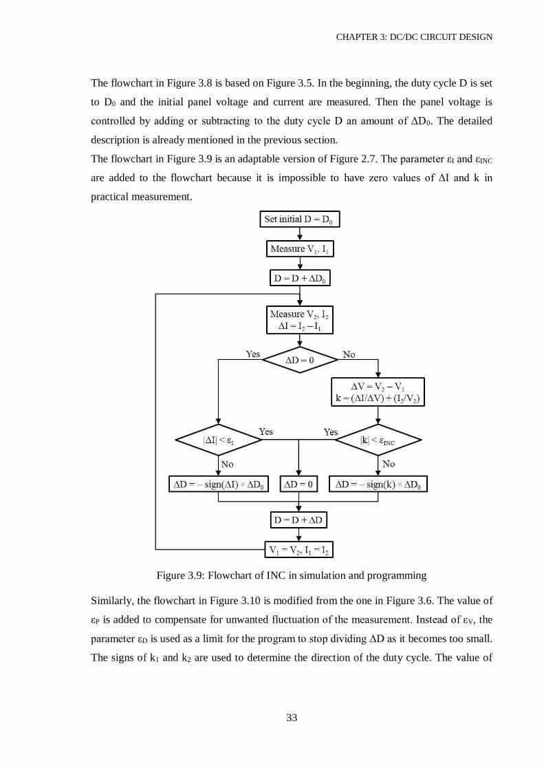
The flowchart in Figure 3.9 is an adaptable version of Figure 2.7. The parameter εI and εINC
are added to the flowchart because it is impossible to have zero values of ΔI and k in
practical measurement.
Figure 3.9: Flowchart of INC in simulation and programming
Similarly, the flowchart in Figure 3.10 is modified from the one in Figure 3.6. The value of
εP is added to compensate for unwanted fluctuation of the measurement. Instead of εV, the
parameter εD is used as a limit for the program to stop dividing ΔD as it becomes too small.
The signs of k1 and k2 are used to determine the direction of the duty cycle. The value of

CHAPTER 3: DC/DC CIRCUIT DESIGN
34
them is not necessary, therefore k2 is calculated as the product of ΔP2 and ΔV2. This avoids
having large values for k2 when ΔV2 is small.
Figure 3.10: Flowchart of BS-P&O in simulation and programming
Hence, the three MPPT algorithms of modified P&O, INC and BS-P&O in Figure 3.5,
Figure 2.7 and Figure 3.6 are refined to suit the practical approach in Figure 3.8, Figure 3.9
and Figure 3.10 respectively. These flowcharts are applied and simulated in the next
section.

CHAPTER 3: DC/DC CIRCUIT DESIGN
35
3.3. Simulation
The simulation model is built on MATLAB/Simulink. A SEPIC is used for testing the
performance of MPPT algorithm. Its output is connected to a resistor R. A capacitor C3 is
put between the PV panel and the SEPIC to reduce drastic change and oscillation of the
panel voltage.
Figure 3.11: MATLAB simulation model for MPPT verification
The MOSFET switch is driven by a PWM block, which operates at the frequency of fsw.
The duty cycle for controlling the switch is updated at the sampling period of Ts.
Component values of the SEPIC circuit are listed in Table 3.2.
C1 = 10μF L1 = 2mH
C2 = C3 = 1000μF L2 = 2mH
Ts = 0.02s R = 5Ω
Table 3.2: Simulation values for SEPIC components
The solar panel used for the simulation is the Perlight Solar PLM-280P-72. The irradiance
is set at 1000W/m2 for the first 0.36s, 800W/m2 from 0.36s to 0.72s and back to 1000W/m2
from 0.72s to 1.08s. The temperature of the solar module is kept constant of 25°C.
D0 = 0.5 ΔD0 = 0.016
εPO = 3.5W εI = 0.04A
εINC = 0.03A/V εD = 0.001
εP = 0.5W fsw = 40kHz
Table 3.3: Simulation values for MPPT parameters

CHAPTER 3: DC/DC CIRCUIT DESIGN
36
In the simulation, the change of duty cycle ΔD0 is set large enough to notice easily. In
practice, it can be chosen for smaller values compared to this simulation. The values of
εPO, εI and εINC are chosen so that the stop conditions are nearly the same for both modified
P&O and INC methods.
Figure 3.12: Modified P&O and INC simulation results
The simulation results of the modified P&O and traditional INC methods with set values in
Table 3.3 to give similar performance are shown in Figure 3.12. At irradiance of
1000W/m2, the operating power point PPV cannot get close to PMPP because of the large
ΔD0. The panel voltage VPV keeps moving up and down or oscillating around the VMPP and
cannot settle down because the |ΔP| is larger than the εPO and the |k| is larger than εINC in
the modified P&O and INC respectively. In this section, the modified P&O and INC
operate as the traditional P&O. At irradiance of 800W/m2, the duty cycle keeps unchanged
but the difference between the operating power point and the MPP is 1.9W. It can be

CHAPTER 3: DC/DC CIRCUIT DESIGN
37
concluded that the two algorithms may not fluctuate in some certain circumstances but not
for all conditions.
Figure 3.13: Binary-Search-Based P&O simulation results
For the BS-P&O result in Figure 3.13, the change of duty cycle ΔD is decreased
exponentially from a large initial value to small values near MPP (in the simulation, ΔD
declines to less than 0.001). This helps operate near the MPP with an error less than 0.05W
in comparison to the theoretic MPP. The response time of the algorithm is less than 0.2s,
which is quick enough for changes of the irradiance. In steady state, the efficiency in the
simulation of the modified P&O and INC is 98.9% and the BS-P&O is 99.9%. Hence,
through the simulation, the new BS-P&O method has been proven to perform better than
the tradition INC and modified P&O methods. Moreover, the novel method has shown its
effectiveness in efficiency and fast response time.

CHAPTER 3: DC/DC CIRCUIT DESIGN
38
Features
Traditional P&O Modified P&O and INC BS-P&O
ΔD0 (fixed) ΔD0 (fixed) εPO, εI, εINC ΔD (variable)
Large Small Large Small Large Small LargeSmall
Accurate
Fast - -
Not fluctuating - -
Table 3.4: Comparison of MPPT methods
Table 3.4 is the summary of the performance of the MPPT methods. For the traditional
P&O, the operating points always fluctuate around the MPP. The step size of the
traditional P&O is fixed. With a large step size, the system can respond quickly to changes
of the environment but the accuracy is low. With a small step size, the system can get a
high MPPT efficiency, however the response time of this method is low. Choosing either
large or a small step size in the traditional P&O would lead to advantage of one feature and
disadvantage of the other.
For a modified P&O and INC, the problem is the same as the traditional P&O for their
fixed step size. However, there are added conditions where the operating points stop
fluctuating. The stop conditions are defined by parameters εPO, εI and εINC. If these
parameters are large, the system may stop at a point which is far from the MPP. But if the
parameters are small, the operating point can stop at a point which is close to the MPP,
however the noise of the measurements can make the system stop at any point. So that, the
stop parameter would be very careful chosen and the measurement noise should be
considered.
For the BS-P&O method, the problems of the P&O and INC are solved by applying
variable step size. The step size is large in the beginning and becomes smaller when the
operating point has just passed the MPP. By doing this, the method can achieve both
accuracy and fast response. The stop condition occurs when the step size gets close to zero
which means that the system stops fluctuate without using stop parameters as in the
modified P&O and INC methods.
The experiment for these MPPT methods are carried out for verifying the theory and
simulation results in section 3.6.2.

CHAPTER 3: DC/DC CIRCUIT DESIGN
39
3.4. Circuit board design
The solar panel used for the experiment is monocrystalline solar module of Perlight Solar
manufacturer. The detail information of this panel at Standard Test Condition (STC) is
listed in Table 3.5. The STC is used to indicate the performance of solar module. A solar
cell at STC has its temperature of 25°C, irradiance of 1000W/m2 and air mass of 1.5
(AM1.5 or solar irradiation angle of 45°).
Figure 3.14: Solar module of the experiment
Manufacturer part number PLM-280M-72
Peak power 𝑃𝑚𝑎𝑥 _𝑆𝑇𝐶 280W
Short circuit current 𝐼𝑠𝑐_𝑆𝑇𝐶 8.32A
Open circuit voltage 𝑉𝑜𝑐_𝑆𝑇𝐶 44.2V
Maximum power current 𝐼𝑚𝑝_𝑆𝑇𝐶 7.73A
Maximum power voltage 𝑉𝑚𝑝_𝑆𝑇𝐶 35.9V
Temperature coefficient of open-circuit voltage 𝜂𝑉𝑜𝑐 –0.333%/°C
Temperature coefficient of power 𝜂𝑃 –0.459%/°C
Power tolerance ±3%
Table 3.5: Technical information of PLM-280M-72 solar module

CHAPTER 3: DC/DC CIRCUIT DESIGN
40
Figure 3.15: Laboratory prototype of DC/DC board
A 10A fuse is put at the input to protect the circuit from unexpected high current. The two
power components, which consume most power, are the MOSFET and diode. Therefore,
two heat-sinks 6399BG with the thermal resistance of 3.3°C/W are used for dissipating
heat from the MOSFET and diode.
The board also includes the power supply circuit, gate driver, sensors and inductors, which
will be presented in the following sections.
3.4.1. Power Supply
The circuit needs power supplies for the sensors and gate drivers of about 5W. The sensor
circuits consist of op-amps and comparators that use a 5V supply. In addition, a 12V
supply is used for the MOSFET gate driver circuits. These 5V and 12V power supplies
will be used for both DC/DC and DC/AC boards. The estimated power of all the sensor,
gate-driver and control circuits is 4W for 5V power supply and 1W for 12V supply or the
output current of 0.8A for 5V supply and 0.083A for 12V supply.
The source for the power supplies can be taken from the input of the PV panel or from the
battery. There are two common methods of regulating from high to low voltage.
The first way is using the linear regulators. However, the power losses are considerable.
For the PV input of 35V, the power losses of these regulators are:

CHAPTER 3: DC/DC CIRCUIT DESIGN
41
Ploss_5V = (Vin – 5) × Iout = (35 – 5) × 0.8 = 24W (3.47)
Ploss_12V = (Vin – 12) × Iout = (35 – 12) × 0.083 = 1.9W (3.48)
The loss of the linear regulators is large, so that the switching regulators TL2575HV-05
and TL2575HV-12 are chosen. These regulators are able to output the 1A current with the
efficiency about 80%. This means the power loss of both is less than the one of linear
regulators. The highest operation voltage of these regulators is 60V, which is higher than
the open-circuit voltage 𝑉𝑜𝑐 of the solar module. However, extra components will be used
for these ones.
Figure 3.16: Schematic of 5V and 12V power supplies
Among the external components, two inductors of 330μH and 680μH are used. The
combination of tantalum and electrolytic capacitors help stabilize voltage and reduce noise.
The electrolytic capacitors with high capacitance can maintain the voltage while the
tantalum is used for getting rid of noise and high frequency pulses.
There are two diodes, which are put at the output of the input sources VPV and Vbat. The
supply can be taken from both PV panel and battery. One of the two diodes will conduct
when one of the two voltage levels is higher than the other. This helps to provide the
source uninterruptedly at night or in shaded conditions.
3.4.2. MOSFET gate driver
To switch the MOSFET on and off with a control signal from a microcontroller, a gate
driver circuit is needed. In this application, TC4428A is used for driving the MOSFET.
The driver typically has the delay time of 30ns, rise time and fall time of 25ns, which is

CHAPTER 3: DC/DC CIRCUIT DESIGN
42
suitable for switching frequency of the MOSFET. Moreover, TC4428A has one non-
inverting and one inverting driver, which can be used for not only low-side but also high-
side MOSFET driving applications.
Figure 3.17: Schematic of low-side MOSFET driver
A combination of ceramic and tantalum capacitors between the power supply and ground
of the driver is applied to get rid of noises caused during the switching.
3.4.3. Current sensor
There are many way of measuring current. One of the most common ways is using a
resistor with a very low resistance. The resistor will be connected in series to the circuit
and the current flowing through it makes a voltage drop on this resistor. This voltage value
is then read by a microcontroller and the current value is measured by simply dividing the
voltage drop to the resistance. The resistor needs to be small enough that it will not
consume too much power from the source. However, if the value of resistor is too small,
the voltage drop in it is small too and it is challenging to read the exact value of current.
Figure 3.18: Current transducer LTS 6-NP

CHAPTER 3: DC/DC CIRCUIT DESIGN
43
The other way of measuring current is using the Hall Effect. This kind of current
measurement is energy effective and precise. The current transducer LTS 6-NP is chosen
for it has bidirectional current input and multiple ranges. Because the current can flow bi-
directionally, it can be used for both DC and AC measurement. Moreover, with multiple
ranges this sensor may be adjusted for different current levels. The maximum current value
that can pass through it is 19.2A and the accuracy of this sensor is ±0.2% which is suitable
for this application. The sensor voltage supply is 5V, which is available from the circuit. In
addition, there is no external component needed.
3.4.4. Voltage sensor
The PV voltage is above 30V but the maximum input voltage for a microcontroller is 3.3V.
Therefore, a simple voltage follower with an op-amp is applied.
Figure 3.19: Schematic of DC voltage sensor
The input voltage is stepped down by two resistors R1 and R2 before coming to the op-
amp. The relation of the input and output voltages is shown in the equation below.
Vout =
R2
R1 + R2Vin (3.49)
In the experiment, the maximum input voltage of the solar panel at 0°C and irradiation of
1000W/m2 is calculated as:
𝑉𝑜𝑐_0℃ = 𝑉oc _𝑆𝑇𝐶(1 + 𝜂𝑉𝑜𝑐(0 − 𝑇𝑆𝑇𝐶)) (3.50)
or 𝑉𝑜𝑐_0℃ = 44.2(1 + 0.00333 × 25) = 47.9V (3.51)
The output voltage should be less than 3.3V, therefore:
R2
R1 + R247.9 ≤ 3.3 (3.52)

CHAPTER 3: DC/DC CIRCUIT DESIGN
44
or R1
R2≥ 13.5 (3.53)
Choose R1 of 150kΩ and R2 of 10kΩ. The ratio of R1 to R2 is 15 and the ratio of the input
to output voltage is 16.
3.4.5. Inductor and capacitor conditions
The chosen switching frequency for the SEPIC is 40kHz. The noise is created at switching
frequency by reactive components such as inductors and transformer. The human hearing
frequency ranges from 20Hz to 20kHz, so that the switching frequency needs to be higher
than this range to make the noise inaudible to human ears. The size of inductors is
proportionally reduced when the switching frequency is increased or the higher the
frequency gives a smaller inductor. Nonetheless, too high value of frequency causes
difficulties in designing the MOSFET gate-drivers and control, thus 40kHz was selected
for this project.
The conditions for inductance and capacitance values can be determined by the chosen
switching frequency. The solar panel in the experiment has the maximum power of 280W.
In the case of just 100W output is obtained, as seen in the datasheet of the solar panel, the
panel voltage at MPP is about 33V, so that the output current is calculated as 3A. From the
equation (3.38), the condition of 𝐿1 is calculated as below:
𝐿1 ≥
𝐷𝑚𝑎𝑥
2𝑓(
𝑉𝐼
𝐼𝐼)
𝑚𝑎𝑥
=1
2 × 40000
33
3= 0.14mH (3.54)
Similar to the 𝐿1 inductor, the condition of inductor 𝐿2 is taken from equation (3.40) as:
𝐿2 ≥
𝐷𝑚𝑎𝑥
2𝑓(
𝑉𝑂
𝐼𝑂)
𝑚𝑎𝑥
=1
2 × 40000
33
3= 0.14mH (3.55)
The next step is the condition of capacitor 𝐶1 from equation (3.42). The maximum input
current of the solar panel is 8A, so that the output current is chosen for the case of 10A.
The input voltage of the solar panel is at around the MPP and is taken as 30V.
𝐶1 ≥
𝐼𝑂_𝑚𝑎𝑥𝐷𝑚𝑎𝑥
2𝑉𝐼_𝑚𝑖𝑛𝑓=
10 × 1
2 × 30 × 40000= 4.17μF (3.56)
Hence, the chosen capacitor 𝐶1 is 10μF metallized polypropylene film capacitor. This kind
of capacitor is bipolar and suitable for high frequency switching. The values of two
inductors are chosen as twice the calculated value or 𝐿1 = 𝐿2 = 0.28mH.

CHAPTER 3: DC/DC CIRCUIT DESIGN
45
3.4.6. Inductor design
Unlike capacitors, which may be bought in the market by the rating of capacitance and
voltage range, inductors for switching power applications have to be designed and wound
separately.
3.4.6.1. Methodology
An inductor consists of a winding, magnetic core and an air gap. The function of the core
is to conduct magnetic field and increase the effect of the magnetic force. A core usually
includes an air gap which has a number of advantages. First, it stores most of the energy of
an inductor. Second, with the same limit of core saturation, the current flowing in the
winding with an air gap can reach higher values than without the air gap. Third, the air gap
is less dependent on temperature than the core, so it helps the inductance value be more
stable than the core without an air gap.
Figure 3.20: Basic E-core inductor
General formulas:
The formula of inductance of an inductor is:
𝐿 =
𝑁2
ℛ𝑒𝑞 (3.57)

CHAPTER 3: DC/DC CIRCUIT DESIGN
46
Where 𝑁 is the number of winding turns, ℛ𝑒𝑞 is the equivalent magnetic reluctance of the
inductor and it consists of reluctances of core ℛ𝑐 and the air gap ℛ𝑔.
ℛ𝑒𝑞 = ℛ𝑐 + ℛ𝑔 (3.58)
ℛ𝑒𝑞 =
𝑙𝑐
𝜇𝑟𝜇0𝐴𝑐+
𝑙𝑔
𝜇0𝐴𝑐=
𝑙𝑐
𝜇𝑒𝜇0𝐴𝑐 (3.59)
with 𝜇𝑒 = (1
𝜇𝑟+
𝑙𝑔
𝑙𝑐)
−1
(3.60)
where 𝑙𝑐 is the effective magnetic path length, 𝑙𝑔 is the length of the air gap, 𝐴𝑐 cross-
sectional area of core, 𝜇0 is the magnetic permeability of free space, 𝜇𝑟 is the relative
permeability and 𝜇𝑒 is the effective relative permeability of the core.
From equations (3.57) and (3.59), the inductance value of an inductor is calculated as:
𝐿 =
𝑁2𝜇𝑒𝜇0𝐴𝑐
𝑙𝑐 (3.61)
Litz wire application:
To reduce the effect of Eddy current, Litz wires are used for winding the coil. In this
design, 7 insulated strands are used and they are twisted together to make a Litz wire. Litz
wire has the advantage of reducing the effect of Eddy current losses since it contains
several small diameter strand wires. Moreover, the Litz wire may be easier to bend in
comparison to a large solid conductor. For carrying large value of current, several Litz
wires are used.
In this section, the formulas are mainly based on the book “Transformers and inductors for
power electronics” [54]. In this book, the formulas are applied for single-conductor
winding, thus they are different for Litz wires. Therefore, all the formulas will be
constructed for this application.
Figure 3.21: Litz wire

CHAPTER 3: DC/DC CIRCUIT DESIGN
47
Let 𝐴𝑠𝑡𝑟𝑎𝑛𝑑 be the area, 𝑑𝑠𝑡𝑟𝑎𝑛𝑑 be the diameter of each strand. Also for the Litz wire,
𝑛𝐿𝑖𝑡𝑧 is the number of Litz wires and 𝐴𝐿𝑖𝑡𝑧 is the overall area of a Litz wire. The diameter
of the Litz wire is approximately three times larger than the strand wire, therefore:
𝐴𝐿𝑖𝑡𝑧 = 9𝐴𝑠𝑡𝑟𝑎𝑛𝑑 (3.62)
Because of winding by hand, the ratio of the winding to the window area of the core is 𝑘𝑢.
The relation of the cross-sectional area of the winding to the core window area 𝐴𝑤𝑑 is
shown in the following equation.
𝑁𝐴𝐿𝑖𝑡𝑧𝑛𝐿𝑖𝑡𝑧 = 9𝑁𝑛𝐿𝑖𝑡𝑧𝐴𝑠𝑡𝑟𝑎𝑛𝑑 = 𝑘𝑢𝐴𝑤𝑑 (3.63)
The Litz wire is made of seven strand wires so that the resistance of the winding 𝑅𝑤𝑖𝑟𝑒 is
calculated by the resistance of a strand wire divided by seven. In the case of 𝑛𝐿𝑖𝑡𝑧 Litz
wires, the winding resistance is reduced because of 𝑛𝐿𝑖𝑡𝑧 connected in parallel.
𝑅𝑤𝑖𝑟𝑒 =
𝜌𝑙𝑤𝑖𝑟𝑒
7𝑛𝐿𝑖𝑡𝑧𝐴𝑠𝑡𝑟𝑎𝑛𝑑=
𝜌𝑁𝑙𝑡𝑢𝑟𝑛
7𝑛𝐿𝑖𝑡𝑧𝐴𝑠𝑡𝑟𝑎𝑛𝑑 (3.64)
where 𝜌 is the resistivity of conductor and 𝑙𝑡𝑢𝑟𝑛 is the mean length of a turn of winding
wires. The winding wires have resistance so that there is power loss 𝑃𝑤𝑖𝑟𝑒 when the current
flows. Let 𝐼𝐿_𝑟𝑚𝑠 be the RMS current and 𝑘𝑖 be the ratio between RMS and the maximum
values of current.
𝑃𝑤𝑖𝑟𝑒 = 𝑅𝑤𝑖𝑟𝑒𝐼𝐿_𝑟𝑚𝑠
2 =𝜌𝑁𝑙𝑡𝑢𝑟𝑛
7𝑛𝐿𝑖𝑡𝑧𝐴𝑠𝑡𝑟𝑎𝑛𝑑𝑘𝑖
2𝐼𝐿_𝑚𝑎𝑥2 (3.65)
or 𝐼𝐿_𝑚𝑎𝑥 =1
𝑘𝑖√
7𝑛𝐿𝑖𝑡𝑧𝐴𝑠𝑡𝑟𝑎𝑛𝑑 𝑃𝑤𝑖𝑟𝑒
𝜌𝑁𝑙𝑡𝑢𝑟𝑛 (3.66)
Also the relationship of inductor current and the flux density is that the largest current
flowing to the inductor 𝐼𝐿_𝑚𝑎𝑥 causes the flux density to get its maximum value 𝐵𝑚𝑎𝑥.
𝐼𝐿_𝑚𝑎𝑥 =
𝐵𝑚𝑎𝑥𝑙𝑐
𝜇𝑒𝜇0𝑁 (3.67)
Calculating optimum effective permeability:
As seen in (3.65) and (3.67), the higher the current, the higher the power loss and flux
density. The dissipation value of the core has to be larger than the loss value of the
winding. It is needed for an optimum condition where the maximum current still makes the
core under saturation and be lower than the dissipation value. The optimum effective
relative permeability 𝜇𝑒_𝑜𝑝𝑡 occurs when 𝐵𝑚𝑎𝑥 = 𝐵𝑠𝑎𝑡 and power loss of the winding wire

CHAPTER 3: DC/DC CIRCUIT DESIGN
48
equals to the maximum dissipation of the winding 𝑃𝐷 or 𝑃𝑤𝑖𝑟𝑒 = 𝑃𝐷 [54]. From equations
(3.67) and (3.66), the value of 𝜇𝑒_𝑜𝑝𝑡 is calculated as following:
𝜇𝑒_𝑜𝑝𝑡 =𝐵𝑚𝑎𝑥𝑘𝑖𝑙𝑐
𝜇0
√9𝜌𝑙𝑡𝑢𝑟𝑛
7𝑃𝐷𝑘𝑢𝐴𝑤𝑑 (3.68)
Where 𝑃𝐷 is calculated by the change in temperature ∆𝑇 and the thermal resistance 𝑅𝜃 of
the core.
𝑃𝐷 = ∆𝑇/𝑅𝜃 (3.69)
The value of thermal resistance 𝑅𝜃 can be found in the datasheet of the manufacturer. But
in case that the value is not provided, it can be calculated by the volume of the core 𝑉𝑐 as:
𝑅𝜃 = 0.06/√𝑉𝑐 (3.70)
Calculating current density:
The next step is to calculate the current density and it is shown as follow:
𝐽0 =
𝐼𝐿_𝑟𝑚𝑠
7𝑛𝐿𝑖𝑡𝑧𝐴𝑠𝑡𝑟𝑎𝑛𝑑 (3.71)
The relationship between winding loss and current density is taken from equation (3.65):
𝑃𝑤𝑖𝑟𝑒 = 7𝜌𝑁𝑙𝑡𝑢𝑟𝑛𝑛𝐿𝑖𝑡𝑧𝐴𝑠𝑡𝑟𝑎𝑛𝑑𝐽02 (3.72)
The volume of the wire winding 𝑉𝑤 is calculated from equation (3.63) as below:
𝑉𝑤 = 𝑙𝑡𝑢𝑟𝑛𝐴𝑤𝑑 = 9𝑙𝑡𝑢𝑟𝑛𝑁𝑛𝐿𝑖𝑡𝑧𝐴𝑠𝑡𝑟𝑎𝑛𝑑/𝑘𝑢 (3.73)
Combining equations (3.72) and (3.73):
𝑃𝑤𝑖𝑟𝑒 =
7
9𝜌𝑉𝑤𝑘𝑢𝐽0
2 (3.74)
Besides the winding loss 𝑃𝑤𝑖𝑟𝑒, there is loss from the core 𝑃𝑐𝑜𝑟𝑒. These two power losses
are related by the ratio 𝛾. The total loss of the inductor 𝑃𝑙𝑜𝑠𝑠 is calculated as:
𝑃𝑐𝑜𝑟𝑒 = 𝛾𝑃𝑤𝑖𝑟𝑒 (3.75)
and 𝑃𝑙𝑜𝑠𝑠 = 𝑃𝑐𝑜𝑟𝑒 + 𝑃𝑤𝑖𝑟𝑒 = (1 + 𝛾)𝑃𝑤𝑖𝑟𝑒 (3.76)
Moreover, the total loss 𝑃𝑙𝑜𝑠𝑠 depends on the change of temperature ∆𝑇, heat transfer
coefficient ℎ𝑐 and the core surface area 𝐴𝑡.
𝑃𝑙𝑜𝑠𝑠 = ℎ𝑐𝐴𝑡∆𝑇 (3.77)
then (1 + 𝛾)𝑃𝑤𝑖𝑟𝑒 =7
9(1 + 𝛾)𝜌𝑉𝑤𝑘𝑢𝐽0
2 = ℎ𝑐𝐴𝑡∆𝑇 (3.78)
Let 𝐴𝑝 be the product of core window area 𝐴𝑤𝑑 and cross-sectional area 𝐴𝑐. The values of
𝑉𝑤 and 𝐴𝑡 are related with 𝐴𝑝 through coefficients 𝑘𝑤 and 𝑘𝑎. These coefficients vary for

CHAPTER 3: DC/DC CIRCUIT DESIGN
49
different types of cores. The typical values of these is found based on extensive studies of
several core types and sizes that 𝑘𝑤 = 10 and 𝑘𝑎 = 40 [54].
𝐴𝑝 = 𝐴𝑐𝐴𝑤𝑑 (3.79)
𝑉𝑤 = 𝑘𝑤𝐴𝑝3/4
(3.80)
𝐴𝑡 = 𝑘𝑎𝐴𝑝1/2
(3.81)
From (3.78) to (3.81), the current density is:
𝐽0 =1
√𝐴𝑝8
√9ℎ𝑐𝑘𝑎∆𝑇
7𝜌𝑘𝑤𝑘𝑢(1 + 𝛾)=
𝑘𝑡
√𝐴𝑝8
√9∆𝑇
7𝑘𝑢(1 + 𝛾) (3.82)
with 𝑘𝑡 = √ℎ𝑐𝑘𝑎
𝜌𝑘𝑤 (3.83)
Calculating inductor size:
Combining these equations (3.61), (3.67), (3.71) and (3.79), then:
𝐿𝐼𝐿_𝑚𝑎𝑥
2 =𝐵𝑚𝑎𝑥𝐴𝑝𝑘𝑢𝐽0
𝑘𝑖 (3.84)
After that, substitute 𝐽0 from equation (3.82) to the (3.84), the value of 𝐴𝑝 is calculated as:
𝐴𝑝 = (𝑘𝑖𝐿𝐼𝐿_𝑚𝑎𝑥
2
𝑘𝑡𝐵𝑚𝑎𝑥
√7(1 + 𝛾)
9𝑘𝑢∆𝑇)
87
(3.85)
Those above equations are used for calculating and choosing the size for the inductor. The
following are the steps taken.
Calculating air gap length:
First, the size of the core is determined by the value of 𝐴𝑝 from equation (3.85). After that,
the length of air gap is chosen by the value of 𝜇𝑒_𝑜𝑝𝑡 from equation (3.68).
𝑙𝑔 ≤
𝑙𝑐
𝜇𝑒_𝑜𝑝𝑡 (3.86)
With the chosen air gap length 𝑙𝑔, the number of turns is calculated as below:
𝑁 = √𝐿/𝐴𝐿 (3.87)
where 𝐴𝐿 is the induction factor and depends on the length of the air gap. If the value of
the induction factor is not provided, it may be calculated as following:
𝐴𝐿 =
𝜇0𝐴𝑐
(𝑙𝑐
𝜇𝑟+
𝑙𝑔
𝑘𝑔)
(3.88)

CHAPTER 3: DC/DC CIRCUIT DESIGN
50
With 𝑘𝑔 is the air gap correction coefficient and is the practical correction for 𝑙𝑔. The table
below shows the values of 𝑘𝑔 [55].
𝑙𝑔 (mm) 0.1 0.2 0.5 1.0 2.0 3.0 4.0
𝑘𝑔 1.1 1.2 1.3 1.4 1.5 1.65 1.8
Table 3.6: Values of the air gap correction
Calculating Litz wire:
The next step is choosing the size of the strand wires. The diameter of the wire should be
close to half of the skin depth 𝛿.
𝛿 = √𝜌
𝜋𝑓𝜇0 (3.89)
and 𝑑𝑠𝑡𝑟𝑎𝑛𝑑 ≈𝛿
2 (3.90)
With the chosen wire size, the number of Litz wire needed to use for carrying enough
current is calculated through the current density 𝐽0 from equation (3.71):
𝑛𝐿𝑖𝑡𝑧 =
𝑘𝑖𝐼𝐿_𝑚𝑎𝑥
7𝐽0𝐴𝑠𝑡𝑟𝑎𝑛𝑑 (3.91)
Calculating the power losses:
The following step is determining the wire and core losses. The power loss of the winding
is calculated:
𝑃𝑤𝑖𝑟𝑒 = 𝑅𝑤𝑖𝑟𝑒𝐼𝐿_𝑟𝑚𝑠
2 =𝜌𝑁𝑙𝑡𝑢𝑟𝑛
7𝑛𝐿𝑖𝑡𝑧𝐴𝑠𝑡𝑟𝑎𝑛𝑑𝐼𝐿_𝑟𝑚𝑠
2 (3.92)
with 𝜌 = 𝜌0[1 + 𝛼0(𝑇𝑚𝑎𝑥 − 20)] (3.93)
The core loss is proportional to the volume 𝑉𝑐 of the core, the frequency 𝑓 of current and
the change of flux density ∆𝐵.
𝑃𝑐𝑜𝑟𝑒 = 𝑉𝑐𝑘𝑐𝑜𝑟𝑒𝑓𝛼 (
∆𝐵
2)
𝛽
(3.94)
Where 𝛼, 𝛽 and 𝑘𝑐𝑜𝑟𝑒 are coefficients of material making the core.
3.4.6.2. Calculation for the inductor
The material for the core of this application is ferrite N87, which is suitable for high
frequency. With the initial conditions in the table below, the size of the core will be

CHAPTER 3: DC/DC CIRCUIT DESIGN
51
determined. The maximum operating temperature of both the core and winding wire is
155°C, so that the maximum temperature 𝑇𝑚𝑎𝑥 for calculation is taken half of it or 70°C.
𝐿 = 0.28mH 𝑘𝑢 = 0.5 𝐵𝑚𝑎𝑥 = 0.2T
𝐼𝐿_𝑚𝑎𝑥 = 8.5A 𝛾 = 0 𝑘𝑐𝑜𝑟𝑒 = 16.9
𝑘𝑖 = 1 ∆𝑇 = 40°C 𝛼 = 1.25
𝑓 = 40kHz 𝑇𝑚𝑎𝑥 = 70°C 𝛽 = 2.35
Table 3.7: Initial values for calculating inductor
From equation (3.85), 𝐴𝑝 is calculated as:
𝐴𝑝 = ((0.28 × 10−3) × 8.52
(48.2 × 103) × 0.2√
7
9 × 0.5 × 40)
87
= 5.07cm4 (3.95)
Choose the core ETD49 which has the 𝐴𝑝_𝐸𝑇𝐷49 = 5.8cm4.
𝐴𝑤𝑑 = 2.75cm2 𝑙𝑡𝑢𝑟𝑛 = 8.7cm 𝑉𝑐 = 24.1cm3
𝐴𝑐 = 2.11cm2 𝜇𝑟 = 1630 𝑙𝑐 = 11.4cm
Table 3.8: Specifications of ferrite core ETD49 [56]
Thermal resistance can be taken from equation (3.70) as:
𝑅𝜃 = 0.06/√24.1 × 10−6 = 12.2℃/W (3.96)
Therefore, the maximum dissipation power of the core is:
𝑃𝐷 = 40/12.2 = 3.27W (3.97)
From equation (3.93), the resistivity of conductor at the temperature of 𝑇𝑚𝑎𝑥 is:
𝜌 = (1.72 × 10⁻⁸)[1 + 0.004(70 − 20)] = (2.06 × 10⁻⁸)Ωm (3.98)
Then the optimum effective relative permeability is taken from equation (3.68) as:
𝜇𝑒_𝑜𝑝𝑡 =0.2 × 0.114
4𝜋 × 10−7√
9(2.06 × 10−8) × 0.087
7 × 3.27 × 0.5 × (2.75 × 10−4)= 41.13 (3.99)
The condition for choosing the gap length is then taken from equation (3.86):
𝑙𝑔 ≤
0.114
41.13= 2.77mm (3.100)
Choose the length of air gap 𝑙𝑔=2.5mm, then to calculate the number turn, the value of 𝐴𝐿
needs to be determined. However, the datasheet of the core does not show the value for a

CHAPTER 3: DC/DC CIRCUIT DESIGN
52
gap of 2.5mm. Therefore, it is determined from equation (3.88). From Table 3.6, the value
of 𝑘𝑔 is calculated as 1.575, then:
𝐴𝐿 =
(4𝜋 × 10−7)(2.11 × 10⁻⁴)
(0.1141630 +
(2.5 × 10⁻³)1.575 )
= 1.6nH (3.101)
The number of turn is calculated from equation (3.87):
𝑁 = √(0.28 × 10⁻³)/(1.6 × 10−9) = 41.8 (3.102)
Choose 𝑁 = 42 turns. The next step is to determine the size of winding wire. First, the
skin depth is calculated:
𝛿 = √(2.06 × 10⁻⁸)
40000𝜋(4𝜋 × 10−7)= 0.362mm (3.103)
From the condition in (3.90), choose 𝑑𝑠𝑡𝑟𝑎𝑛𝑑 = 0.4mm or 𝐴𝑠𝑡𝑟𝑎𝑛𝑑 = 0.136mm2. The
current density is calculated as below from equation (3.82):
𝐽0 =(48.2 × 10³)
√(5.8 × 10⁻⁸)8√
9 × 40
7 × 0.5= 3.924A/mm2 (3.104)
Use the value of 𝐽0 to calculate the number Litz wires 𝑛𝐿𝑖𝑡𝑧 from equation (3.91):
𝑛𝐿𝑖𝑡𝑧 =
8.5
7(3.924 × 10⁶)(0.136 × 10⁻⁶)= 2.28 (3.105)
Choose 𝑛𝐿𝑖𝑡𝑧 = 3. From equation (3.63), the window utilization factor is calculated as:
𝑘𝑢_𝑎𝑓𝑡𝑒𝑟 =
9𝐴𝑠𝑡𝑟𝑎𝑛𝑑𝑛𝐿𝑖𝑡𝑧𝑁
𝐴𝑤𝑑=
9 × (0.136 × 10−6) × 3 × 42
(2.75 × 10⁻⁴)= 0.56 (3.106)
The window utilization factor is about 0.6 which is hard for winding manually. Therefore,
the designer should make the winding very carefully. Parameters needed for making an
inductor are now all calculated. The laboratory inductors are shown in Figure 3.22.
The next step is to calculate the power loss of the inductor. From equation (3.65), the wire
loss is then calculated as:
𝑃𝑤𝑖𝑟𝑒 =
(2.06 × 10−8) × 42 × 0.087 × 8.52
7 × 3 × (0.136 × 10−6)= 1.91W (3.107)
Core loss is determined with the value ∆𝐵 = 0.2T which is chosen to be equal the
maximum flux density of the core. Therefore from equation (3.94), 𝑃𝑐𝑜𝑟𝑒 is calculated as:
𝑃𝑐𝑜𝑟𝑒 = (24.1 × 10−6) × 16.9 × 400001.25 (
0.2
2)
2.35
= 1.03W (3.108)

CHAPTER 3: DC/DC CIRCUIT DESIGN
53
Then the total loss of the core and the winding is:
𝑃𝑙𝑜𝑠𝑠 = 1.03 + 1.91 = 2.94W (3.109)
The maximum total loss of one inductor is calculated of 2.94W. The loss in practical
operation may be less than this value because the loss is calculated in the most extreme
condition.
Figure 3.22: Implemented inductors
In Figure 3.23, the inductance of the implemented inductor is measured by an LCR meter
and the result is 0.280mH which is the exact value needed.
In comparison to the method using single wire, the core size is calculated as below [54].
𝐴𝑝_𝑠𝑖𝑛𝑔𝑙𝑒 = (𝑘𝑖𝐿𝐼𝐿_𝑚𝑎𝑥
2
𝑘𝑡𝐵𝑚𝑎𝑥√
1 + 𝛾
𝑘𝑢∆𝑇)
87
(3.110)
The difference between the method of using a single conductor and using Litz wires is:
𝐴𝑝_𝐿𝑖𝑡𝑧
𝐴𝑝_𝑠𝑖𝑛𝑔𝑙𝑒= (√7/9)
87 = 0.866 (3.111)
From equation above, the core size using single conductor is 15% larger than the core
using Litz wires.

CHAPTER 3: DC/DC CIRCUIT DESIGN
54
Figure 3.23: Measurement of the inductor
3.5. Programming
A Tiva C Series TM4C123G LaunchPad Evaluation Board from Texas Instruments is used
for control system. The board includes In-circuit Debug Interface (ICDI) that allows easy
programming and debugging of the microcontroller. It also includes two PWM modules
and two 12-bit Analog-to-Digital Converter (ADC) modules, which are convenient to get
measured quantities and control all power converters.
Figure 3.24: Pin diagram of TM4C123G LaunchPad Evaluation Board [57]

CHAPTER 3: DC/DC CIRCUIT DESIGN
55
Figure 3.25: Tiva C Series TM4C123G LaunchPad Evaluation Board [58]
The environment for programming is the CCS software, which the values of variables in
the microcontroller memory can be exported to a laptop.
Timer0 is set at 50Hz and is used for updating duty cycle and measuring values of voltage
and current.
To measure current and voltage values of PV, the ratio of real voltage and sensor is
measured in advance. As mentioned in section 3.4.4, the ratio of voltage is measured of
14.1, therefore the PV voltage is calculated as the equation below.
VPV = (VADC×3.3/4095)×14.1 (3.112)
For the current, the formula is based on the datasheet of the current transducer.
IPV = ((VADC×3.3/4095)×1.03 – 2.524)×9.6 (3.113)
Pins PD0 and PD1 are taken to be the input pins to measure PV current and voltage
respectively.
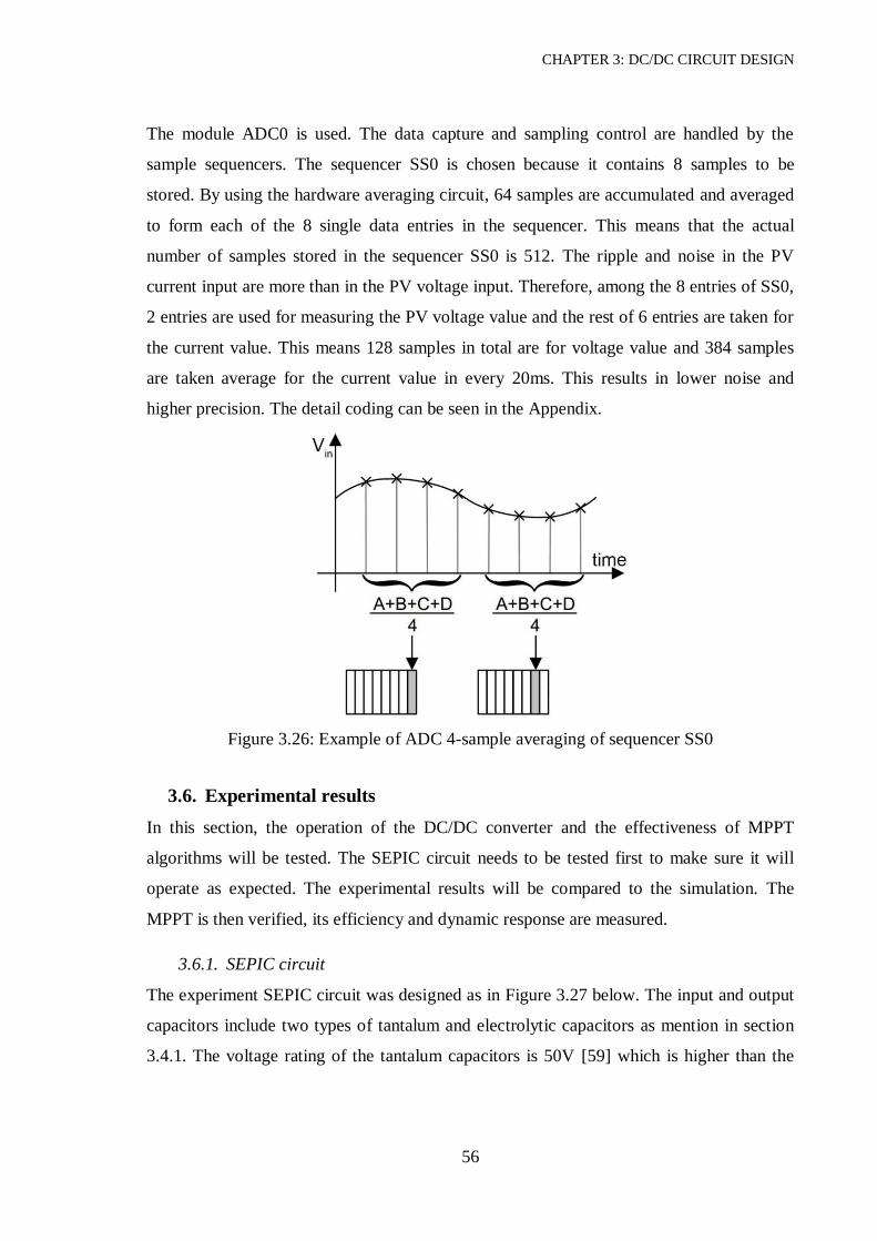
CHAPTER 3: DC/DC CIRCUIT DESIGN
56
The module ADC0 is used. The data capture and sampling control are handled by the
sample sequencers. The sequencer SS0 is chosen because it contains 8 samples to be
stored. By using the hardware averaging circuit, 64 samples are accumulated and averaged
to form each of the 8 single data entries in the sequencer. This means that the actual
number of samples stored in the sequencer SS0 is 512. The ripple and noise in the PV
current input are more than in the PV voltage input. Therefore, among the 8 entries of SS0,
2 entries are used for measuring the PV voltage value and the rest of 6 entries are taken for
the current value. This means 128 samples in total are for voltage value and 384 samples
are taken average for the current value in every 20ms. This results in lower noise and
higher precision. The detail coding can be seen in the Appendix.
Figure 3.26: Example of ADC 4-sample averaging of sequencer SS0
3.6. Experimental results
In this section, the operation of the DC/DC converter and the effectiveness of MPPT
algorithms will be tested. The SEPIC circuit needs to be tested first to make sure it will
operate as expected. The experimental results will be compared to the simulation. The
MPPT is then verified, its efficiency and dynamic response are measured.
3.6.1. SEPIC circuit
The experiment SEPIC circuit was designed as in Figure 3.27 below. The input and output
capacitors include two types of tantalum and electrolytic capacitors as mention in section
3.4.1. The voltage rating of the tantalum capacitors is 50V [59] which is higher than the

CHAPTER 3: DC/DC CIRCUIT DESIGN
57
input and output of the circuit so that they can be placed in parallel to the large electrolytic
capacitors for reducing noise.
Figure 3.27: Experimental SEPIC circuit for performance testing
The duty cycle D is set to the value of 0.5, so that from equation (3.23), the input and
output voltage theoretically should be equal to each other. The DC input voltage of SEPIC
is set to be 15.6V and the output is connected to a 6Ω resistor. The MATLAB simulation
of the SEPIC whose component values are the same as in Figure 3.27 is also conducted
and put to the graph with the experimental results for comparison.
Figure 3.28: Experiment result of SEPIC input and output voltages
In Figure 3.28, the measured output voltage is 14.6V, which is 1V less than the input level
because of the voltage drop of the output diode. In comparison to the input voltage, the
output voltage does not consist of large ripples. The following figures show the voltage
waveforms of components in the circuit.

CHAPTER 3: DC/DC CIRCUIT DESIGN
58
In Figure 3.29, the 𝐶1 voltage oscillated around the input voltage of 15.6V. From equation
(3.34), the voltage ripple of the capacitor is calculated as:
∆𝑣𝐶1=
𝐷𝐼𝑂
𝐶1𝑓=
𝐷𝑉𝑂
𝐶1𝑓𝑅=
0.5 × 14.6
(10 × 10−6) × 40000 × 6= 3V (3.114)
As seen in Figure 3.29, the voltage variation of the capacitor 𝐶1 is around 3V which is
similar to the calculated one. Besides, the capacitor voltage consists of high frequency
harmonics but they are not too high to affect the output results of the converter.
Figure 3.29: Experiment and simulation results of SEPIC 𝐶1 voltage
In Figure 3.30, the voltage of 𝐿1 is in positive side when the switch is closed and in
negative side when the switched is opened. When 𝑉𝐿1is positive, its value is 15.6V which
is equal the input voltage. At the negative side, the voltage ripples is about 3V which is
similar to the ripple in the capacitor 𝐶1.
Figure 3.30: Experiment and simulation results of SEPIC 𝐿1 voltage

CHAPTER 3: DC/DC CIRCUIT DESIGN
59
Similar to the 𝐿1, in Figure 3.31, the voltage of the inductor 𝐿2 is positive when the
switched is closed and negative when the switch is opened. The average value in the
positive side equal to 15.6V and the voltage variation is also around 3V. In both
waveforms of the two inductors, the high frequency contents still exist but their amplitudes
are small and are filtered by the capacitor at the output.
Figure 3.31: Experiment and simulation results of SEPIC 𝐿2 voltage
As seen in Figure 3.32, the switch voltage is nearly zero when it is closed. When the
switch is opened, the measured average value is 31.1V which as twice as the input voltage.
As the theory shown in Figure 3.2, the rise of the voltage when the switch is opened equals
to the sum of ripples in the capacitor 𝐶1 and the output voltage. Since the output voltage
has insignificant ripple so that the voltage rise of the switch when it is opened is similar to
the ripple of 𝐶1 or 3V.
Figure 3.32: Experiment and simulation results of SEPIC switch voltage

CHAPTER 3: DC/DC CIRCUIT DESIGN
60
In Figure 3.33, the diode voltage is negative when the switch is closed and its average
value is about -31V. When the switch is opened, the diode conducts and the voltage drop
on it is measured about 1V.
Figure 3.33: Experiment and simulation results of SEPIC diode voltage
In conclusion, the results from the experiment are similar to the theory depicted in Figure
3.2. Therefore, the design of SEPIC satisfies the continuous mode and qualifies for the
next step, which is the testing the effectiveness of MPPT methods.
3.6.2. MPPT test
The test for MPPT was carried out in the Zero2020 electrical control room of Cork
Institute of Technology.
Figure 3.34: MPPT testing set-up

CHAPTER 3: DC/DC CIRCUIT DESIGN
61
DC wires from the tested solar module are routed to the room for the experiment. The
voltage and current values of the panel are recorded in the microcontroller memory and
then are read by the CCS software installed in a laptop.
The circuit is connected as Figure 3.35 below. The component values of the SEPIC circuit
are the same as in Figure 3.27. The voltage and current sensors are connected to get data
for the microcontroller. The microcontroller makes decisions using the MPPT algorithm
and outputs the PWM signal to the MOSFET gate driver for controlling the circuit.
Figure 3.35: Block connection of the MPPT testing
The output of the SEPIC is connected to four 1.5Ω–100W resistors connected in series
giving an equivalent 6Ω–400W output resistor. The maximum output power of PV panel is
about 280W and voltage of 35V, therefore a 6Ω resistor is suitable.
Figure 3.36: Output resistors for MPPT testing
Controlling and switching frequencies for the circuit are the same as the Table 3.3. Other
controlling values for the experiment are: εP = 1 W, εD = 0.001. Current and voltage values
are obtained by the ADC of the microcontroller every 0.02s.

CHAPTER 3: DC/DC CIRCUIT DESIGN
62
Two criteria for an MPPT method are the efficiency of the algorithm and the response time
to the change in irradiance.
3.6.2.1. Efficiency test
In the test, the pyranometer SP Lite2 [60] is used for measuring the incident irradiance. It
is placed and tilted with the same angle as the tested solar module.
Figure 3.37: Pyranometer SP Lite2
The output power of the solar module depends not only the irradiance but also the
temperature of the panel.
Figure 3.38: PV Current-Voltage curve of different temperatures [61]
In Figure 3.38, the MPP of the PV module decrease when the cell temperature increases.
To determine the efficiency of the algorithm, the power at MPP taken from the solar panel
is theoretically calculated as below. The parameters are taken from Table 3.5.

CHAPTER 3: DC/DC CIRCUIT DESIGN
63
𝑃𝑀𝑃𝑃 = 𝑃max _𝑆𝑇𝐶
𝐺
𝐺𝑆𝑇𝐶
(1 + 𝜂𝑃(𝑇 − 𝑇𝑆𝑇𝐶)) (3.115)
or 𝑃𝑀𝑃𝑃 = 280𝐺
1000(1 − 0.00459(𝑇 − 25)) (3.116)
Where 𝐺 is the irradiance value read from the pyranometer. The temperature 𝑇 is taken
from the temperature sensor installed under a solar module, which is near the tested one as
in Figure 3.39 below.
Figure 3.39: Temperature sensor location for the experiment
The efficiency of the MPPT algorithm is then calculated by the formula below.
𝜂𝑀𝑃𝑃𝑇 =
𝑃𝑚𝑒𝑎𝑠𝑢𝑟𝑒𝑑
𝑃 𝑀𝑃𝑃 (3.117)
There are errors in measurement from the solar module power tolerance, temperature and
irradiance sensors. In addition, because there is just one solar module for the experiments,
each test is conducted in a specific condition and the experiments for different MPPT
methods are carried out in different time, irradiation and temperature. Thus, the results of
the experimental efficiency are relative and used for comparison among different MPPT
algorithms.
In this experiment, the algorithms are tested to investigate the most efficient method and
validate the simulation and theory. In Figure 3.40, the results of modified P&O are
presented. As the previous discussion, the voltage fluctuation leads to ripples in the power

CHAPTER 3: DC/DC CIRCUIT DESIGN
64
result. In the experiment, the algorithm operates as the traditional P&O because the |ΔP| is
larger than the value εPO as shown in the simulation section. The efficiency of this method
is 96.76%.
Figure 3.40: Experiment and simulation results of modified P&O
The experimental results of BS-P&O algorithm are shown in Figure 3.41. The efficiency of
this method is measured at 99.23%. It is 2.5% higher than the tested modified P&O.
Moreover, the BS-P&O method makes the PV voltage and current values not vary at the
MPP. In addition, it can be seen that the time for the algorithm to reach the MPP is fast and
less than 0.2s.

CHAPTER 3: DC/DC CIRCUIT DESIGN
65
Figure 3.41: Experiment and simulation results of BS-P&O
The table below is the summary for the experimental results of the efficiency of the two
methods.
MPPT method Modified P&O BS-P&O
Step size ΔD0 0.016 0.016
Irradiation 𝐺 758W/m2 732W/m2
Temperature 𝑇 40.9°C 46.3°C
𝑃 𝑀𝑃𝑃 196.75W 184.92W
𝑃𝑚𝑒𝑎𝑠𝑢𝑟𝑒𝑑 (average steady state) 190.38W 183.50W
Efficiency 𝜂𝑀𝑃𝑃𝑇 96.76% 99.23%
Ripple (steady state) 5W 0.3W
Table 3.9: Experimental efficiency comparison of MPPT methods
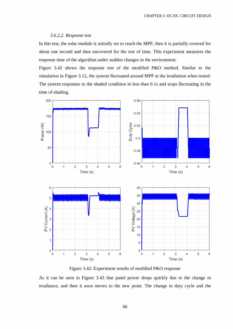
CHAPTER 3: DC/DC CIRCUIT DESIGN
66
3.6.2.2. Response test
In this test, the solar module is initially set to reach the MPP, then it is partially covered for
about one second and then uncovered for the rest of time. This experiment measures the
response time of the algorithm under sudden changes in the environment.
Figure 3.42 shows the response test of the modified P&O method. Similar to the
simulation in Figure 3.12, the system fluctuated around MPP at the irradiation when tested.
The system responses to the shaded condition in less than 0.1s and stops fluctuating in the
time of shading.
Figure 3.42: Experiment results of modified P&O response
As it can be seen in Figure 3.43 that panel power drops quickly due to the change in
irradiance, and then it soon moves to the new point. The change in duty cycle and the

CHAPTER 3: DC/DC CIRCUIT DESIGN
67
voltage are large in the transition and become smaller to get closer to the MPP. The
response time of BS-P&O algorithm is less than 0.2s, which is similar to the simulation
and proves its effectiveness.
Figure 3.43: Experiment results of BS-P&O response
In conclusion, the BS-P&O has been proven the effectiveness and quick response for the
MPPT task from the simulation to the experiment. This method can reach MPP of solar
modules exactly and quickly and is better than the traditional P&O and modified P&O
methods.
In this chapter, the SEPIC was selected and it was proven to meet criteria of the research.
The SEPIC was also used for verifying the novel BS-P&O method which had a better
performance than the modified P&O. The next chapter is the DC/AC circuit design which
includes the power topology and grid measurement method.

CHAPTER 4: DC/AC CIRCUIT DESIGN
68
CHAPTER 4. DC/AC CIRCUIT DESIGN
In this chapter, the design and implementation of the DC/AC converter is presented. The
topology of the converter is tested in simulation and experiment. The design of grid
measurement methods is also mentioned and the sensor circuits are tested with the grid.
4.1. Theory
In this section, the topology of the DC/AC converter is introduced and its operating is
described. In addition, an approach of controlling the inverter to export the active and
reactive powers to the grid is presented.
4.1.1. Power topology
The output voltage of the DC/DC converter is low in comparison to grid level. Therefore,
using a transformer to boost voltage is needed in the DC/AC converter. It is known that
higher the frequency of the signal, the smaller the size of transformer needed. To keep the
size of transformer small, its input should be at high frequency. The topology for the
inverter will be discussed to meet all the above criteria.
Figure 4.1 is the typical 3-level sinusoidal PWM (SPWM) waveform of a H-bridge output.
The PWM waveform is created by comparing a high frequency triangle waveform to a
reference sine waveform. The frequency of SPWM is also the frequency of the triangle
waveform. This SPWM waveform is then filtered to output the pure sinusoidal wave. The
amplitude of the filtered sine wave is depended on the ratio of the reference sine waveform
to the triangle one. The frequency in Figure 4.1 is 4kHz which is used for just the
illustration purpose. With higher frequencies, the PWM waveform cannot be seen. The
frequency used in the application is 40kHz.
In Figure 4.2, the Fast Fourier Transform (FFT) is applied for the waveform which is
similar the one in Figure 4.1 but at the frequency of 40kHz. The main component with the
highest amplitude is at 50Hz with the amplitude of 0.5923, while the carriers of 40050Hz
and 39950Hz have the levels of 0.3619 and 0.3788 respectively. For this reason, the
waveform in Figure 4.1 cannot be used to pass through a high frequency transformer.
Another approach is carried out to avoid the low frequency spectrums.

CHAPTER 4: DC/AC CIRCUIT DESIGN
69
Figure 4.1: Inverter output waveform before filtering at 4kHz (Illustration)
Figure 4.2: FFT analysis of the inverter waveform before filtering at 40kHz in 0.1s

CHAPTER 4: DC/AC CIRCUIT DESIGN
70
Figure 4.3: Waveform to pass through transformer at 4kHz (Illustration)
In Figure 4.3, the pulses of Figure 4.1 are flipped alternatively. By doing this, the
frequency of waveform in Figure 4.1 changes to a much higher frequency one. Again,
4kHz in Figure 4.3 is for illustration purpose. The FFT response of the 40kHz waveform is
shown Figure 4.4 below.
Figure 4.4: FFT analysis of waveform used for transformer at 40kHz in 0.1s
The amplitude component of the 50Hz is just 1.9497×10⁻⁶ and the main component is
0.9179 at 20kHz. Therefore, with a desire output waveform of 40kHz, the frequency pass
through the transformer is half of it or 20kHz.

CHAPTER 4: DC/AC CIRCUIT DESIGN
71
Figure 4.5: Schematic of DC/AC circuit
The final topology of DC/AC converter is shown in Figure 4.5. The first stage is H-bridge,
which creates the high frequency PWM pulses. These pulses then pass through a
transformer to boost the voltage to grid level. After that, a passive diode rectifier bridge is
used to flip all pulses in negative side to positive side. There is no need to have an active
rectifier because the current does not flow backward and the control is much simpler with
the rectifier in comparison to an active switched rectifier. The next stage of the inverter is
the polar reverse bridge to flip pulses at the frequency of 50Hz. And the final stage is LC
filter which blocks all high frequency components and just let the fundamental frequency
signal or 50Hz sinusoidal wave pass through. The passive LC filter is selected for its
simplicity and it does not need to be controlled by the microcontroller.
The 400V is the amplitude of the carrier waveform of the SPWM method. The 400V
square PWM waveform is then filtered by LC filter and outputs the pure sine wave of
230VAC. According to the distribution code, the highest grid voltage is 230VAC+10% or
253VAC. This means the peak voltage of grid is 358V. Therefore, a 400V carrier
waveform is chosen.
The illustration of the waveform at stages of DC/AC topology is shown from Figure 4.6 to
Figure 4.9 below.

CHAPTER 4: DC/AC CIRCUIT DESIGN
72
Figure 4.6: Output voltage of transformer
Figure 4.7: Output voltage of rectifier
Figure 4.8: Output voltage of polar reverse bridge

CHAPTER 4: DC/AC CIRCUIT DESIGN
73
Figure 4.9: Output voltage of filter
The topology of this DC/AC converter is simulated and characterized experimentally in
sections 4.2 and 4.5.
4.1.2. Power control theory
The output of the inverter will pass through an LC filter before connecting to grid. Let the
grid voltage and current be 𝑽𝑔𝑟𝑖𝑑 and 𝑰𝑔𝑟𝑖𝑑, respectively. Also, let 𝑽𝑖𝑛𝑣 and 𝑰𝑖𝑛𝑣 be the
fundamental voltage and current of the inverter before the filter, respectively. A model for
studying power transfer can be built as shown in the figure below.
Figure 4.10: Power transfer model
The capacitor current 𝑰𝑐 and inductor voltage 𝑽𝐿 are calculated as:
𝑰𝑐 = 𝑗𝐶𝜔𝑽𝑔𝑟𝑖𝑑 (4.1)
𝑽𝐿 = 𝑗𝐿𝜔𝑰𝑖𝑛𝑣 (4.2)
Let 𝛿 be the angle between 𝑽𝑔𝑟𝑖𝑑 and 𝑽𝑖𝑛𝑣 as the following figure.
𝑽𝑔𝑟𝑖𝑑 = 𝑉𝑔𝑟𝑖𝑑∠0° (4.3)
𝑽𝑖𝑛𝑣 = 𝑉𝑖𝑛𝑣∠𝛿 = 𝑉𝑖𝑛𝑣(cos 𝛿 + 𝑗 sin 𝛿) (4.4)
Using Kirchhoff’s voltage and current laws of the circuit, so:

CHAPTER 4: DC/AC CIRCUIT DESIGN
74
𝑰𝑖𝑛𝑣 = 𝑰𝑐 + 𝑰𝑔𝑟𝑖𝑑 (4.5)
𝑽𝑖𝑛𝑣 = 𝑽𝐿 + 𝑽𝑔𝑟𝑖𝑑 (4.6)
Figure 4.11: Phasor diagram between grid and inverter voltage
Therefore, the grid current 𝑰𝑔𝑟𝑖𝑑 can be calculated from the above equations as:
𝑰𝑔𝑟𝑖𝑑 =
𝑉𝑖𝑛𝑣 sin 𝛿
𝐿𝜔− 𝑗 (
𝑉𝑖𝑛𝑣 cos 𝛿
𝐿𝜔+ 𝑉𝑔𝑟𝑖𝑑 (𝐶𝜔 −
1
𝐿𝜔)) (4.7)
The complex output power of the grid is:
𝑺 =
1
2𝑽𝑔𝑟𝑖𝑑 𝑰𝑔𝑟𝑖𝑑
∗ (4.8)
or 𝑺 =1
2𝑉𝑔𝑟𝑖𝑑 (
𝑉𝑖𝑛𝑣 sin 𝛿
𝐿𝜔+ 𝑗 (
𝑉𝑖𝑛𝑣 cos 𝛿
𝐿𝜔+ 𝑉𝑔𝑟𝑖𝑑 (𝐶𝜔 −
1
𝐿𝜔))) (4.9)
The active and reactive powers of the output to the grid are then calculated:
𝑃 = 𝑅𝑒(𝑺) =
𝑉𝑔𝑟𝑖𝑑 𝑉𝑖𝑛𝑣 sin 𝛿
2𝐿𝜔 (4.10)
𝑄 = 𝐼𝑚(𝑺) =
𝑉𝑔𝑟𝑖𝑑
2(
𝑉𝑖𝑛𝑣 cos 𝛿
𝐿𝜔+ 𝑉𝑔𝑟𝑖𝑑 (𝐶𝜔 −
1
𝐿𝜔)) (4.11)
From the two equations above, the value of angle 𝛿 is determined as:
sin 𝛿 =
2𝐿𝜔𝑃
𝑉𝑔𝑟𝑖𝑑 𝑉𝑖𝑛𝑣 (4.12)
cos 𝛿 =
2𝐿𝜔𝑄
𝑉𝑔𝑟𝑖𝑑 𝑉𝑖𝑛𝑣+
𝑉𝑔𝑟𝑖𝑑 𝐿𝜔
𝑉𝑖𝑛𝑣(
1
𝐿𝜔− 𝐶𝜔) (4.13)
And with Pythagorean Theorem of:
sin2𝛿 + cos2𝛿 = 1 (4.14)
The peak value of inverter output 𝑉𝑖𝑛𝑣 and the angle 𝛿 is then calculated.
𝑉𝑖𝑛𝑣 =2𝐿𝜔
𝑉𝑔𝑟𝑖𝑑
√𝑃2 + (𝑄 +𝑉𝑔𝑟𝑖𝑑
2
2(
1
𝐿𝜔− 𝐶𝜔))
2
(4.15)

CHAPTER 4: DC/AC CIRCUIT DESIGN
75
and 𝛿 = sin−1 (2𝐿𝜔𝑃
𝑉𝑔𝑟𝑖𝑑𝑉𝑖𝑛𝑣) (4.16)
Hence, from equations (4.15) and (4.16) the amplitude and phase angle of the inverter can
be calculated by grid amplitude 𝑉𝑔𝑟𝑖𝑑 , active power 𝑃 and reactive power 𝑄. The grid
amplitude 𝑉𝑔𝑟𝑖𝑑 can be measured by the sensor at the inverter output. The active power 𝑃
is the MPP taken from the solar panel through the DC/DC converter. The reactive 𝑄 is
usually set to be zero and it is set in the case of supporting the grid.
4.2. Simulation
MATLAB model is used for simulating the DC/AC converter and verifying the controlling
theory in section 4.1.2. The model is designed and shown in Figure 4.12 and values used
for the simulation are listed in Table 4.1.
Figure 4.12: MATLAB simulation model DC/AC converter
P = 200W Q = 20VAR
C = 0.1μF L = 20mH
R1 = 0.1Ω R2 = 10Ω
fgrid = 50Hz fH-bridge = 40kHz
VDC = 30VDC Vgrid = 230VAC (325.269V peak)
Table 4.1: Simulation values for inverter parameters
The inverter is set to output the active power of 200W and reactive power of 20VAR. The
output of the inverter is connected to the grid of 230VAC and 50Hz. In the model, the H-
bridge is controlled by signals LL and LR and the polar reverse bridge is switched by the
signal R. These control signals are program to output the PWM based on the reference
signal calculated from equations (4.15) and (4.16). From these equations the peak output of
the inverter 𝑉𝑖𝑛𝑣 is calculated as 322.9823V and the phase angle 𝛿 is 1.384°.

CHAPTER 4: DC/AC CIRCUIT DESIGN
76
Figure 4.13: Simulated output voltage and current of polar reverse bridge
Figure 4.14: Simulated output voltage and current of filter

CHAPTER 4: DC/AC CIRCUIT DESIGN
77
Figure 4.15: Simulated output active power and reactive power of inverter
From Figure 4.15, it can be seen that the output power of the inverter can be controlled by
the phase and amplitude of the grid as shown in the equations (4.15) and (4.16).
Figure 4.16: Inverter amplitude and phase angle versus output power
In Figure 4.16, the calculated amplitude 𝑉𝑖𝑛𝑣 and phase angle 𝛿 are calculated for different
active power 𝑃 values. It can be seen that the change in 𝑉𝑖𝑛𝑣 and 𝛿 are too small for every
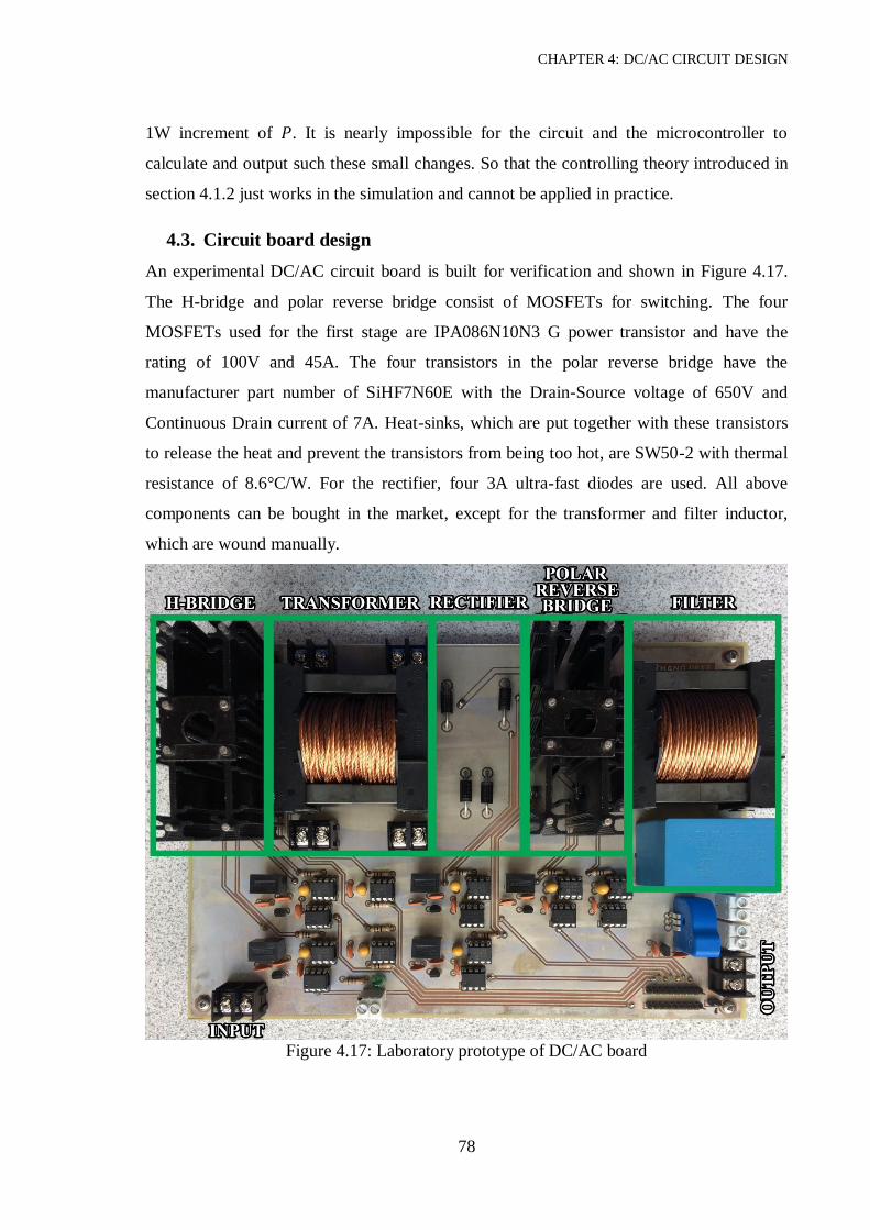
CHAPTER 4: DC/AC CIRCUIT DESIGN
78
1W increment of 𝑃. It is nearly impossible for the circuit and the microcontroller to
calculate and output such these small changes. So that the controlling theory introduced in
section 4.1.2 just works in the simulation and cannot be applied in practice.
4.3. Circuit board design
An experimental DC/AC circuit board is built for verification and shown in Figure 4.17.
The H-bridge and polar reverse bridge consist of MOSFETs for switching. The four
MOSFETs used for the first stage are IPA086N10N3 G power transistor and have the
rating of 100V and 45A. The four transistors in the polar reverse bridge have the
manufacturer part number of SiHF7N60E with the Drain-Source voltage of 650V and
Continuous Drain current of 7A. Heat-sinks, which are put together with these transistors
to release the heat and prevent the transistors from being too hot, are SW50-2 with thermal
resistance of 8.6°C/W. For the rectifier, four 3A ultra-fast diodes are used. All above
components can be bought in the market, except for the transformer and filter inductor,
which are wound manually.
Figure 4.17: Laboratory prototype of DC/AC board

CHAPTER 4: DC/AC CIRCUIT DESIGN
79
4.3.1. Transformer design
Similar to the design of inductors in the DC/DC section, the transformer needed to be
designed for specific voltage ratings, input power, transformer ratio and frequency.
4.3.1.1. Methodology
In this section, a 2-coil transformer is considered. The purpose of re-building the formulas
from the book [54] is that the Litz wire is used instead of a single conductor. Therefore,
some steps, which do not affect the change of formulas, will be skipped. Moreover, same
parameters, which are mentioned in the inductor design, will not be defined again in this
section.
Figure 4.18: Basic E-core 2-coil transformer
General equations:
The equation below shows the input power 𝑃𝑖𝑛 is related with elements which are
mentioned in the inductor design section and the waveform factor 𝑘𝑣.
2𝑃𝑖𝑛 = 𝑓𝑘𝑣𝑘𝑢𝐵𝑚𝑎𝑥𝐴𝑝𝐽0 (4.17)
The area of the winding 𝐴𝑤 consists of the primary and secondary windings.
𝐴𝑤 = 9𝑁𝑝𝑛𝐿𝑖𝑡𝑧_𝑝𝐴𝑠𝑡𝑟𝑎𝑛𝑑_𝑝 + 9𝑁𝑠𝑛𝐿𝑖𝑡𝑧_𝑠𝐴𝑠𝑡𝑟𝑎𝑛𝑑_𝑠 = 𝑘𝑢𝐴𝑤𝑑 (4.18)
Power loss:
The power loss of the wire consists with two parts of primary and secondary sides.
𝑃𝑤𝑖𝑟𝑒 = 𝑅𝑤𝑖𝑟𝑒_𝑝𝐼𝑟𝑚𝑠_𝑝2 + 𝑅𝑤𝑖𝑟𝑒_𝑠𝐼𝑟𝑚𝑠_𝑠
2 (4.19)

CHAPTER 4: DC/AC CIRCUIT DESIGN
80
or 𝑃𝑤𝑖𝑟𝑒 = 𝜌𝑙𝑡𝑢𝑟𝑛 (𝑁𝑝𝐼𝑟𝑚𝑠_𝑝
2
7𝑛𝐿𝑖𝑡𝑧_𝑝𝐴𝑠𝑡𝑟𝑎𝑛𝑑_𝑠+
𝑁𝑠𝐼𝑟𝑚𝑠_𝑠2
7𝑛𝐿𝑖𝑡𝑧_𝑠𝐴𝑠𝑡𝑟𝑎𝑛𝑑_𝑠) (4.20)
Current density 𝐽0 is equal in both primary and secondary sides, so:
𝐽0 =
𝐼𝑟𝑚𝑠_𝑝
7𝑛𝐿𝑖𝑡𝑧_𝑝𝐴𝑠𝑡𝑟𝑎𝑛𝑑_𝑝=
𝐼𝑟𝑚𝑠_𝑠
7𝑛𝐿𝑖𝑡𝑧_𝑠𝐴𝑠𝑡𝑟𝑎𝑛𝑑_𝑠 (4.21)
Combine the equations (4.18), (4.20) and (4.21), the power loss of the winding is:
𝑃𝑤𝑖𝑟𝑒 = 7𝜌𝑙𝑡𝑢𝑟𝑛𝐽02(𝑛𝐿𝑖𝑡𝑧_𝑝𝐴𝑠𝑡𝑟𝑎𝑛𝑑_𝑝𝑁𝑝 + 𝑛𝐿𝑖𝑡𝑧_𝑠𝐴𝑠𝑡𝑟𝑎𝑛𝑑_𝑠𝑁𝑠) (4.22)
or 𝑃𝑤𝑖𝑟𝑒 =7
9𝜌𝑙𝑡𝑢𝑟𝑛𝐽0
2𝑘𝑢𝐴𝑤𝑑 (4.23)
With volume of the winding is
𝑉𝑤 = 𝑙𝑡𝑢𝑟𝑛𝐴𝑤𝑑 (4.24)
So combine (4.23) and (4.24), the power loss of the winding 𝑃𝑤𝑖𝑟𝑒 is then:
𝑃𝑤𝑖𝑟𝑒 =
7
9𝜌𝑉𝑤𝑘𝑢𝐽0
2 (4.25)
The total loss in the transformer is defined as in equations (3.76) and (3.77) with 𝛾 = 1.
𝑃𝑙𝑜𝑠𝑠 = ℎ𝑐𝐴𝑡∆𝑇 = 2𝑃𝑤𝑖𝑟𝑒 (4.26)
so ℎ𝑐𝐴𝑡∆𝑇 =14
9𝜌𝑉𝑤𝑘𝑢𝐽0
2 (4.27)
Calculating current density:
Thus, from equation (4.27), the current density 𝐽0 of transformer is calculated as:
𝐽0 = √9ℎ𝑐𝐴𝑡Δ𝑇
14𝜌𝑉𝑤𝑘𝑢 (4.28)
With 𝐴𝑡, 𝑉𝑤 and 𝑘𝑡 are defined in the equations below.
𝐴𝑡 = 𝑘𝑎𝐴𝑝1/2
(4.29)
𝑉𝑤 = 𝑘𝑤𝐴𝑝3/4
(4.30)
and 𝑘𝑡 = √ℎ𝑐𝑘𝑎
𝜌𝑘𝑤 (4.31)
Then the current density 𝐽0 from equation (4.28) is:
𝐽0 = 𝑘𝑡√9Δ𝑇
14𝑘𝑢
1
√𝐴𝑝8
(4.32)
Calculating transformer size:
From equations (4.17) and (4.32), 𝐴𝑝 is calculated as follows:

CHAPTER 4: DC/AC CIRCUIT DESIGN
81
𝐴𝑝 = (2𝑃𝑖𝑛
𝑓𝑘𝑡𝑘𝑣𝐵𝑚𝑎𝑥√
14
9𝑘𝑢Δ𝑇)
87
(4.33)
Calculating optimum flux density:
The following equation is used for calculating the optimum flux density 𝐵𝑜:
(
𝑃𝑙𝑜𝑠𝑠
2)
23
= 𝑃𝑤𝑖𝑟𝑒
112 𝑃𝑐𝑜𝑟𝑒
712 (4.34)
Where 𝑃𝑐𝑜𝑟𝑒 is the core loss and is similar to the equation (3.94). Taken 𝛽 = 2, the core
loss is then calculated by the optimum flux density 𝐵𝑜 as:
𝑃𝑐𝑜𝑟𝑒 = 𝑉𝑐𝑘𝑐𝑜𝑟𝑒𝑓𝛼𝐵𝑜𝛽
= 𝑉𝑐𝑘𝑐𝑜𝑟𝑒𝑓𝛼𝐵𝑜2 (4.35)
Hence, combining three equations (4.25), (4.26) and (4.35) to equation (4.34):
(ℎ𝑐𝐴𝑡∆𝑇
2)
23
= (7
9𝜌𝑘𝑤𝐴𝑝
34 𝑘𝑢𝐽0
2)
112
(𝑘𝑐𝐴𝑝
34 𝑘𝑐𝑜𝑟𝑒𝑓𝛼𝐵𝑜
2)
712
(4.36)
or (ℎ𝑐𝑘𝑎∆𝑇
2)
23
= (7
9𝜌𝑘𝑤𝑘𝑢)
112
(𝑘𝑐𝑘𝑐𝑜𝑟𝑒𝑓𝛼𝐵𝑜2)
712(𝐴𝑝𝐽0)
16 (4.37)
Taken 𝐴𝑝𝐽0 from equation (4.17), then:
𝐴𝑝𝐽0 =
2𝑃𝑖𝑛
𝑓𝑘𝑣𝑘𝑢𝐵𝑜 (4.38)
After that, substitute 𝐴𝑝𝐽0 from equation (4.38) to (4.37), the value of 𝐵𝑜 is calculated.
𝐵𝑜 =(
12 ℎ𝑐𝑘𝑎∆𝑇)
23
(79 𝜌𝑘𝑤𝑘𝑢)
112
(𝑘𝑐𝑘𝑐𝑜𝑟𝑒𝑓𝛼)7
12 (2𝑃𝑖𝑛
𝑓𝑘𝑣𝑘𝑢)
16
(4.39)
The value of optimum flux density 𝐵𝑜 should not be larger than the saturation value 𝐵𝑠𝑎𝑡.
Calculating winding turns:
Finally, the number of primary winding turns is determined as the formula below.
𝑁𝑝 =
𝑉𝑟𝑚𝑠_𝑝
2𝑘𝑣𝑓𝐵𝑜𝐴𝑐 (4.40)
The value of secondary turns 𝑁𝑠 will be calculated through 𝑁𝑝 and the transformer ratio.
4.3.1.2. Calculation for the transformer
Similar to calculating inductor, a ferrite core is chosen for this application. The transformer
is used to boost the low voltage of battery to grid level. Then the initial values needed for
calculating are listed in the following table.

CHAPTER 4: DC/AC CIRCUIT DESIGN
82
𝑓 = 20kHz 𝑘𝑢 = 0.5 ∆𝑇 = 30°C
𝑃𝑖𝑛 = 280W 𝑘𝑣 = 4 𝑇𝑚𝑎𝑥 = 70°C
𝑉𝑟𝑚𝑠_𝑝 = 33.6V 𝑁𝑠/𝑁𝑝 = 14 𝐵𝑠𝑎𝑡 = 0.2T
Table 4.2: Initial values for calculating transformer
First from (4.39), the optimum flux density is calculated.
𝐵𝑜 =(
12 × 10 × 40 × 30)
23
(79
(2.06 × 10−8) × 10 × 0.5)
112
(5.6 × 16.9 × 200001.25)7
12 (2 × 280
20000 × 4 × 0.5)
16
= 0.135T (4.41)
The value of 𝐵𝑜 is less than the saturation flux density 𝐵𝑠𝑎𝑡 of ferrite core, then the next
step is carried out. The core size is determined from equation (4.33) as follows.
𝐴𝑝 = (2 × 280
20000 × (48.2 × 103) × 4 × 0.13√
14
9 × 0.5 × 30)
87
= 4.14cm4 (4.42)
Choose the core ETD49 which has the 𝐴𝑝_𝐸𝑇𝐷49 = 5.8cm4. Specifications of the coil are
based on the Table 3.8. From equation (4.40), the number of primary turns is calculated as
below:
𝑁𝑝 =
33.6
2 × 4 × 20000 × 0.13 × (2.11 × 10−4)= 7.4 (4.43)
Choose 𝑁𝑝 = 8 turns. With the ratio of 14, therefore 𝑁𝑠 = 112 turns. The core loss of the
transformer is calculated from equation (4.35).
𝑃𝑐𝑜𝑟𝑒 = (2.41 × 10−5) × 16.9 × 200001.250.1352 = 1.76W (4.44)
The current density is calculated from equation (4.32):
𝐽0 = (48.2 × 10³)√9 × 30
14 × 0.5
1
√(5.8 × 10⁻⁸)8= 2.4A/mm2 (4.45)
The power loss of the winding is taken from equation (4.23) and the value of 𝜌 is the same
as in equation (3.98):
𝑃𝑤𝑖𝑟𝑒 =7
9(2.06 × 10−8) × 0.087 × (2.4 × 106)2 × 0.5 × (2.75 × 10−4) = 0.66W (4.46)
Therefore, the total power loss of the transformer is then:
𝑃𝑙𝑜𝑠𝑠 = 𝑃𝑐𝑜𝑟𝑒 + 𝑃𝑤𝑖𝑟𝑒 = 1.76 + 0.66 = 2.42W (4.47)
After winding, the measured inductance of the primary side is 0.272mH and the inductance
of the secondary side is 53.6mH. Similar to the equation (3.111), the core size using Litz
wires is 15% smaller than the core size using a single conductor.

CHAPTER 4: DC/AC CIRCUIT DESIGN
83
4.3.2. Grid measuring
To synchronize to the grid, the frequency, phase and amplitude values need to be
determined. To measure the grid values, a small transformer is used to step down the high
voltage of grid to the lower level for the microcontroller.
Figure 4.19: Laboratory prototype of grid sensing board
Because the input grid voltage is bipolar, 5V and -5V power supplies are needed for the
op-amps to operate. The 5V power supply can be taken from the DC/DC board. To get -5V
supply from 5V, a voltage converter ICL7660 is used.
Figure 4.20: ICL7660 circuit of -5V supply
In this research, a peak detector is used for capturing the grid voltage amplitude and a zero-
crossing detector (ZCD) is used for measuring the grid frequency and phase. However,
both detectors depend on the grid quantities, which contain not only the fundamental
component, but also a lot of harmonics. An active low-pass filter (LPF) is therefore
required to remove all harmonics.

CHAPTER 4: DC/AC CIRCUIT DESIGN
84
4.3.2.1. Grid filtering
An active filter is a good choice in comparison with a passive filter in signal conditioning
applications. A 2nd-order Sallen-Key Low-pass-filter [62] was selected for the system
under consideration.
Figure 4.21: Schematic circuit of 2nd-order Sallen-Key Low-pass-filter [62]
The cut-off frequency 𝑓𝑐 of this filter is:
𝑓𝑐 =1
2𝜋√𝑅1𝑅2𝐶1𝐶2
=1
2𝜋𝑅𝐶 (4.48)
In the design, the resistor and capacitor values are equal or 𝑅1 = 𝑅2 = 𝑅 and 𝐶1 = 𝐶2 = 𝐶.
With the chosen capacitors of 0.1μF and the cut-off frequency of 150Hz, the resistor value
is then calculated as 10kΩ. With the selected values, the transfer function of this filter is:
𝐻(𝑠) =
1𝑅2𝐶2
𝑠2 +2
𝑅𝐶 𝑠 +1
𝑅2𝐶2
=1000000
𝑠2 + 2000𝑠 + 1000000 (4.49)
The Bode diagram of the transfer function is shown in Figure 4.22.
Figure 4.22: Bode diagram of the active filter

CHAPTER 4: DC/AC CIRCUIT DESIGN
85
The filter can get rid of high frequency noise but it causes the signal to be delayed. The
phase delay at the frequency 50Hz is calculated as 34.88° or 1.94ms. This value is verified
by the experiment with a hardware circuit.
4.3.2.2. Grid zero-crossing detector
The circuit for the ZCD is simple and does not consist of many components. The grid
signal will be compared to the zero level or ground. A voltage comparator LM311 is
selected for this task.
Figure 4.23: Schematic circuit of ZCD
The output of ZCD is 5V when the grid voltage is positive and is zero when grid is
negative. By this, the phase and the frequency of grid can be read by the microcontroller.
4.3.2.3. Grid peak detector
The amplitude of grid may vary because of the load, so that it needs to be checked every
cycle. The following Figure 4.24 shows the circuit to measure the grid peak value.
Figure 4.24: Schematic circuit of peak detector

CHAPTER 4: DC/AC CIRCUIT DESIGN
86
An electrolytic capacitor is used to store the maximum value of the input of every cycle.
After storing the peak value in one cycle, the capacitor needs to be discharged for the next
cycle. Therefore, a small PNP transistor is placed in parallel with the capacitor for this
task. The output of ZCD is utilized to switch the transistor on and off. By this way, the
microcontroller requires one less PWM channel and the programming is easier.
4.3.3. MOSFET gate driver
The controlling PWM signals are generated by the microcontroller. The design of the low-
side driver is similar to the one of DC/DC converter circuit. The challenge of this part is to
design a high-side MOSFET driver.
The optocoupler HCPL-2400 is used. Its output is inverted, so that the output of the
optocoupler is connected to the inverting driver of TC4428.
Figure 4.25: Schematic of high-side MOSFET driver
For the high-side driver circuit, not only the input signals but also the power supplies need
to be isolated. The converter RI-1212S is used for converting 12V input to isolated 12V
output.
Figure 4.26: Schematic of isolated 5V&12V supplies for MOSFET driver

CHAPTER 4: DC/AC CIRCUIT DESIGN
87
The isolated 5V supply is taken from a linear converter 78L05 because this power supply
is just used for the optocoupler. The HCPL-2400 current load is 4mA, so that the power
loss in the 78L05 is about 28mW which is acceptable.
4.4. Programming
There are H-bridge and polar reverse bridges in the circuit, therefore two PWM modules 0
and 1 are used. The PWM signals in the H-bridge are at 40kHz while the signals in the
polar reverse bridge are at 50Hz.
4.4.1. SPWM generating
There are many methods to generate the SPWM to the H-bridge. The first way is using the
analog generators by comparing a reference sinusoidal wave to a triangular one. This way
requires a lot of components and has noise.
The other way is using a digital method to calculate the sine values by the microcontroller.
However, getting sine values in the microcontroller requires many calculating cycles and
the microcontroller needs to work harder and longer for every switching cycle.
A simple digital way to get the SPWM output is a look-up table. In this method, values of
sine are pre-calculated and stored in a table. For the switching frequency of 40kHz and the
grid output frequency of 50Hz, there are 800 sine values for every cycle of 20ms. Because
the sine wave is symmetric, a half of these values or 400 points are enough for generating
the whole cycle.
Figure 4.27: Example of 50Hz sine values with sampling of 4kHz

CHAPTER 4: DC/AC CIRCUIT DESIGN
88
4.4.2. Frequency control
Because the grid frequency is not fixed and may vary around 50Hz, the output PWM
should be adapted to the grid frequency. The distribution code for transmission systems
states that the frequency of normal operation ranges from 49.8Hz to 50.2Hz [48].
Therefore, by adding or removing a few points in the peak of the sine waveform, the
frequency may be controllable. It is nearly flat at the peak of the sinusoidal waveform and
adding or subtracting a few points there does not affect the shape of the output.
At the peak values of frequency or 49.8Hz and 50.2Hz, the algorithm will add or minus at
maximum 4 points for every cycle.
4.4.3. Phase control
Figure 4.28 shows the time delay of the ZCD output with respect to the grid voltage. The
time difference from the falling-edge of the ZCD signal to the grid is 8ms, which is shown
in Figure 4.31.
Figure 4.28: ZCD signal and grid voltage
To synchronize the grid with the ZCD input, the output of the PWM needs to be delayed
by the program. For the switching of 40kHz frequency or 25μs period, the program will
delay 320 cycles or 8ms for synchronizing to the grid.
4.4.4. Operation
The flowchart of the programming is shown in Figure 4.29. The signals of LL, LR and R
are the PWM output to control the MOSFETs as shown in Figure 4.12. There are two
interrupts in the coding which are the 40kHz PWM timer and the falling-edge of the ZCD
signal.

CHAPTER 4: DC/AC CIRCUIT DESIGN
89
Figure 4.29: Simple flowchart of inverter programming

CHAPTER 4: DC/AC CIRCUIT DESIGN
90
The 40kHz PWM interrupt is used to update the duty cycle values for controlling the
switches. The values of LL and LR are determined by an array Dsin pre-calculated and
stored in the microcontroller memory. Because the output waveform of the H-bridge is at
high frequency, LL and LR are updated alternately or LL is updated duty cycle while LR is
turned off and vice versa.
The ZCD interrupt occurs when the falling-edge of the signal is detected by the
microcontroller. This interrupt is used for counting the period of the grid, the counted point
pcount is set to be zero when the ZCD interrupt happens. Then pcount is incremented in each
25μs period and should be 800 with a standard grid frequency of 50Hz.
The controlling signal R is used for switching the Polar Reverse Bridge at 50Hz therefore
it does not need to be updated as fast as the LL and LR. The updating frequency of R is the
same as the ZCD interrupt.
In the flowchart in Figure 4.29, the ADC of grid peak is not mentioned because the output
voltage of the inverter is controlled manually. The detail program is shown in the
Appendix.
4.5. Experimental results
The designed circuit is built to verify the prototype and the coding. In the experiment, the
transformer, low-side and high-side gate drivers are evaluated. The sensor circuit is also
tested before experimenting with the inverter.
The connection of the experiment is shown in Figure 4.30. Instead of connecting to the
grid, the output of the inverter is connected to a resistor.
Figure 4.30: Block connection of the experiment

CHAPTER 4: DC/AC CIRCUIT DESIGN
91
Grid voltage is connected to the sensor circuit for measuring the frequency and amplitude
of the grid. The outputs of the sensors are then read by a microcontroller. After that, the
microcontroller outputs the PWM signals to the gate-driver circuits to drive the MOSFETs
of the H-bridge and polar reverse bridge.
4.5.1. Grid measuring
The grid measurement is important for the coding and synchronizing of the inverter. The
sensor circuit includes ZCD, peak detector and filter, which were calibrated and measured
to compensate the delay time and peak ratio data for the programming.
4.5.1.1. Grid filtering
As mentioned previously, a small transformer is used for decreasing the grid voltage. The
output of the transformer is then passed through an active filter to get rid of unexpected
noise and harmonic spectrums. This is important because the accuracy of the sensor
depends on the quality of the input signal. Figure 4.31 below shows the grid voltage and
the filtered signal from the transformer.
Figure 4.31: Grid voltage and grid filtered signal
The output of the signal transformer has the phase leading the grid voltage, and it is
measured of 0.4ms. The theory calculation of the phase lag of the filter is 1.94ms as

CHAPTER 4: DC/AC CIRCUIT DESIGN
92
mentioned in 4.3.2.1. So the phase lag of the filtered signal to the grid is 1.54ms. The
measured phase lag of the filtered signal to the grid voltage is 2ms. The difference of the
calculated value to the measure one is 0.46ms which is caused by the tolerance of
component values. The phase-shifted value is used for the programming.
4.5.1.2. Grid zero-crossing detector
The circuit design and the output of the ZCD are simple, but this signal is very important
for controlling both the frequency and phase angle of the grid. As can be seen in Figure
4.32, the output voltage of the ZCD immediately change from zero to a higher level when
the input signal changes from negative to positive values. By measuring the time between
two consecutive falling-edges of ZCD signals, the period of the grid can be collected.
Moreover, the rising-edge and falling edge also indicate the phase of the grid when it
passes zero.
Figure 4.32: Zero-crossing detector output and grid filtered signal
4.5.1.3. Grid peak detector
The peak detector in section 4.3.2.3 stores the maximum input value to the capacitor and
then discharges it for the next period. As seen in Figure 4.33, during half of the grid period,
the output signal of the peak detector increases its level and maintains its highest value. In

CHAPTER 4: DC/AC CIRCUIT DESIGN
93
the other half, the capacitor voltage drops slowly for refreshing to the next period. The
maximum value of the input signal is kept unchanged for a quarter of the period till the
falling-edge of the ZCD signal. Therefore, in the coding, the falling-edge interrupt is
chosen instead of rising-edge.
Figure 4.33: Peak detector output and grid filtered signal
4.5.2. DC/AC circuit
After testing the measuring sensors, the circuit performance is then experimentally
measured. The input of the circuit is a 30VDC source and the output is connected to a
1.13kΩ resistor.
In Figure 4.34, the output of the transformer is shown and it is at 20kHz frequency. In a
transformer, there are many parasitic parameters such as inter-winding capacitance, self-
capacitance and winding resistance. The parasitic capacitance values are the cause of the
ringing of the transformer waveform [63]. The winding of the transformer is made
manually so that the effect of the parasitic values is high. The ripples and overshoot of this
signal are nearly double the signal but after the LC filter, the output of the inverter is clear
of high frequency harmonics and synchronized to the frequency and phase of the grid as
shown in Figure 4.35.

CHAPTER 4: DC/AC CIRCUIT DESIGN
94
Figure 4.34: Experimental result of transformer output voltage
Figure 4.35: Experimental result of the inverter output
In the experiment, the inverter was not connected to the grid. In Figure 4.35, the grid
voltage and the inverter output nearly match each other in amplitude, frequency and phase.

CHAPTER 4: DC/AC CIRCUIT DESIGN
95
The circuit is built for verification purposes and this result has proven the topology of the
DC/AC converter.
The output of the DC/AC converter was connected to a resistor. The connection between
the inverter and the grid were not conducted. The output amplitude of the inverter was set
manually because there were problems with the coding and gate driver circuit. The
microcontroller worked with the interrupt input of ZCD and the inverter could export a
sinusoidal output voltage which was synchronized to the grid frequency. The ADC module
was supposed to read the data from the peak detector and updated every cycle of the grid
frequency. However, when adding the ADC module to the programming code, one of the
PWM output pins was broken by the feedback current of the gate driver circuit.
In conclusion, the DC/AC converter and the sensor circuits were tested for their
performances. The experimental results were proven the topology of the DC/AC converter.
The converter could export the output which was similar to the theory and the simulation.
However, there were problems in coding and the implementation of the circuit which made
the incompleteness of the experiment for the grid connection.

CHAPTER 5: CONCLUSION
96
CHAPTER 5. CONCLUSION
In this section, the achievements, contributions and the successful work of this project are
presented. In addition, during the time of the research, there were problems and difficulties
in implementation and experiments. Proposed solutions for the problems and
improvements are suggested in the future work.
5.1. Achievements
The research is to build a micro-inverter, which converts DC power from a solar module to
supply AC grid power. A literature review has been carried out to select a suitable
topology for the converter. The two-stage micro-inverter is chosen with a DC/DC
converter, a DC/AC converter and a Li-ion battery in between.
The selected DC/DC converter is SEPIC and the formulas for its operation and theoretical
waveform of each component were presented in detail. The hardware circuit designed in
this research including sensors, power supplies, heat-sinks and MOSFET gate drivers are
shown. The design of an inductor is described in depth in this research. The inductor is
wound by Litz wires, which perform better than a single conductor. The core size of using
Litz wires is calculated to be 15% smaller than the core size using single conductor. The
implemented SEPIC is tested and the output results are similar to the theory which means
that the circuit meets the design requirements and the continuous current conditions.
The SEPIC is then used for testing the effectiveness of a novel MPPT algorithm called BS-
P&O. A modified P&O method is introduced and then used for comparison to the BS-
P&O. The BS-P&O has been proven to perform better than the traditional P&O, INC and
modified P&O methods in both simulation and experiment. The efficiency of the BS-P&O
is measured to be 1% higher than the traditional methods. The response time for the
sudden change in the environment of this novel algorithm is less than 0.2s, which has been
proven in both simulation and experiment.
The second stage of the micro-inverter is a DC/AC converter, which is more complicated
than the DC/DC converter. The topology is designed for both boosting the low input
voltage to grid level and converting DC to AC at 50Hz. The converter topology and PWM
control are selected for the use of a high frequency transformer. Similar to the inductor, the

CHAPTER 5: CONCLUSION
97
design and winding of the transformer are introduced using Litz wires and the detailed
construction formulas are presented in this research.
The design of grid measurements is also described from theory to practical hardware
circuit. These sensors are able to detect the frequency, amplitude and phase of both grid
current and voltage. The measurement sensors are implemented and tested with the utility
grid and the output results are read by the microcontroller to control MOSFET switches
through PWM signals.
In the simulation, the DC/AC converter is controlled and connected to the utility grid. In
the simulated version, the converter is able to output a pure sinusoidal wave and
synchronize to the grid. It can also transfer active power to the grid by applying the
formulas to control the voltage amplitude and phase of the converter before filtering.
In the experiment, the hardware DC/AC circuit can produce a sinusoidal output that is able
to synchronize to the grid frequency and phase.
5.2. Problems and future work
Physical connection of the inverter to the grid was not carried out in the experiment
because of the time limit and safety requirements. The theory of controlling the converter
voltage and phase to export both active and reactive powers is just applied for the
simulation. In practice, the controlled voltage and phase variations for power level control
are too small for the sensor to measure and the microcontroller to calculate. Therefore, the
approach of current controlling will be applied for the future work. Moreover, the
microcontroller programming is challenged because there are many things involved such
as timers, interrupt, PWM and ADC modules. There are in total 9 PWM outputs and 8
ADC inputs of the microcontroller for controlling both DC/DC and DC/AC circuits.
Therefore, the design of the inverter will be modified for more efficient code execution.
In the process, the DC/DC and DC/AC converters were tested separately without affecting
the other and their combined operation has not yet been experimentally demonstrated. The
effectiveness of the battery as a buffer between these converters will also be considered in
the future.
The use of the battery limits the output voltage of DC/DC converter at a low level. This
requires more components and makes the inverter circuit more complicated to design and
control. More effective and simpler topologies with energy storage will be investigated in
the future studies.

CHAPTER 5: CONCLUSION
98
Lastly, the sensor and gate driver circuits need to be designed in a smaller size and with
less noise by using surface-mount devices (SMD). The method of measuring the grid by
ZCD, peak detector and current sensor may be changed by more powerful devices in the
market.

99
PUBLICATIONS
Chi-Thang Phan-Tan and Nam Nguyen-Quang, “A P&O MPPT method for photovoltaic
applications based on binary-searching,” 2016 IEEE International Conference on
Sustainable Energy Technologies (ICSET), Hanoi, 2016, pp. 78-82.
Chi-Thang Phan-Tan and Nam Nguyen-Quang, “A SEPIC-Based Single-Phase Grid-
Connected Micro-Inverter for Photovoltaic Applications,” 2015 International Symposium
on Electrical and Electronics Engineering (ISEE2015), Ho Chi Minh city, Oct. 2015, pp.
540-549.

100
APPENDIX
Program for MPPT BS-P&O method
#include <stdint.h> #include <stdbool.h> #include <stdlib.h> #include <stdio.h> #include "inc/hw_memmap.h" #include "inc/hw_gpio.h" #include "inc/hw_types.h" #include "inc/tm4c123gh6pm.h" #include "driverlib/sysctl.h" #include "driverlib/gpio.h" #include "driverlib/pin_map.h" #include "driverlib/interrupt.h" #include "driverlib/debug.h" #include "driverlib/adc.h" #include "driverlib/pwm.h" #include "driverlib/timer.h" //********************Variables_[start]********************// uint8_t eP = 2, eD = 1, time = 1; uint16_t i = 0; uint16_t volatile D = 500, dD, dD0 = 16; uint32_t fSW, fSampling; ADC0value[8]; float I1, I2, V1, V2, P1, P2, Vo; float V_d[300], D_d[300], P_d[300]; float dP1 = 1, dP2, dV, k1 = 1, k2; //********************Variables_[end]********************// //********************Main Code_[start]********************// int main(void){
//SysClkFreq = (400MHz/2)/10 = 20MHz SysCtlClockSet(SYSCTL_SYSDIV_10|SYSCTL_USE_PLL|SYSCTL_OSC_MAIN|SYSCTL_XTAL_16MHZ); //=====TIMER0A_[start]=====// SysCtlPeripheralEnable(SYSCTL_PERIPH_TIMER0); //Enable TIMER0 TimerConfigure(TIMER0_BASE, TIMER_CFG_PERIODIC); //TIMER0 fSampling = (SysCtlClockGet()/50); //50Hz = 0.02s TimerLoadSet(TIMER0_BASE, TIMER_A, fSampling); //TIMER0A-50Hz IntEnable(INT_TIMER0A); //TIMER0A TimerIntEnable(TIMER0_BASE, TIMER_TIMA_TIMEOUT); //TIMER0A IntMasterEnable(); TimerEnable(TIMER0_BASE, TIMER_A); //TIMER0A //=====TIMER0A_[end]=====// //=====PWM_setup_[start]=====// //SEPIC_40kHz M1PWM5-PF1 SysCtlPWMClockSet(SYSCTL_PWMDIV_1); //20MHz/1=20MHz for PWM clock SysCtlPeripheralEnable(SYSCTL_PERIPH_PWM1); //PWM Module1 //=====PortF=====// SysCtlPeripheralEnable(SYSCTL_PERIPH_GPIOF); //PortF GPIOPinTypePWM(GPIO_PORTF_BASE, GPIO_PIN_1); //PF1 GPIOPinConfigure(GPIO_PF1_M1PWM5); //PF1[M1PWM5] fSW = (SysCtlClockGet()/40000); //40kHz switching

101
//=====Module1=====// PWMGenConfigure(PWM1_BASE, PWM_GEN_2, PWM_GEN_MODE_DOWN); //GEN2_M1PWM5 PWMGenPeriodSet(PWM1_BASE, PWM_GEN_2, fSW); //GEN2_M1PWM5_40kHz PWMPulseWidthSet(PWM1_BASE, PWM_OUT_5, fSW*D/1000); //M1PWM5, Duty PWMOutputState(PWM1_BASE, PWM_OUT_5_BIT, true); //M1PWM5 PWMGenEnable(PWM1_BASE, PWM_GEN_2); //M1_GEN2 //=====PWM_setup_[end]=====// //=====ADC setup [start]=====// //Ipv AIN7-PD0 & Vpv AIN6-PD1 SysCtlPeripheralEnable(SYSCTL_PERIPH_ADC0); //ADC0
//ADC0 = average of 64 samples ADCHardwareOversampleConfigure(ADC0_BASE, 64);
//ADC0-Sequencer0-8 samples-use default trigger-highest priority
ADCSequenceConfigure(ADC0_BASE, 0, ADC_TRIGGER_PROCESSOR, 0);
//ADC0-Sequencer0-sample0-AIN7 ADCSequenceStepConfigure(ADC0_BASE,0,0,ADC_CTL_CH7);
//ADC0-Sequencer0-sample1-AIN7 ADCSequenceStepConfigure(ADC0_BASE,0,1,ADC_CTL_CH7);
//ADC0-Sequencer0-sample2-AIN7 ADCSequenceStepConfigure(ADC0_BASE,0,2,ADC_CTL_CH7);
//ADC0-Sequencer0-sample3-AIN7 ADCSequenceStepConfigure(ADC0_BASE,0,3,ADC_CTL_CH7);
//ADC0-Sequencer0-sample4-AIN7 ADCSequenceStepConfigure(ADC0_BASE,0,4,ADC_CTL_CH7);
//ADC0-Sequencer0-sample5-AIN7 ADCSequenceStepConfigure(ADC0_BASE,0,5,ADC_CTL_CH7);
//ADC0-Sequencer0-sample6-AIN6 ADCSequenceStepConfigure(ADC0_BASE,0,6,ADC_CTL_CH6);
//ADC0-Sequencer0-sample7-AIN6 ADCSequenceStepConfigure(ADC0_BASE,0,7,ADC_CTL_CH6|ADC_CTL_IE|ADC_CTL_END); ADCSequenceEnable(ADC0_BASE,0); //Enable ADC0-Sequencer0 //=====ADC setup [end]=====// while(1) {} } //********************Main Code [end]********************// //********************TIMER0 Interrupt [start]********************// void TIMER0_Int(void) { TimerIntClear(TIMER0_BASE, TIMER_TIMA_TIMEOUT); //Clear TIMER0 interrupt ADCIntClear(ADC0_BASE, 0); //ADC0-Sequencer0 ADCProcessorTrigger(ADC0_BASE, 0); //ADC0-Sequencer0 while(!ADCIntStatus(ADC0_BASE, 0, false)) //ADC0-Sequencer0 {} ADCSequenceDataGet(ADC0_BASE, 0, ADC0value); //ADC0-Sequencer0 I2 = (((ADC0value[0]+ADC0value[1]+ADC0value[2]+ADC0value[3]+
ADC0value[4]+ADC0value[5])*3.3/(6*4095))*1.03 - 2.524)*9.6; V2 = ((ADC0value[6]+ADC0value[7])*3.3/(2*4095))*14.1; P2 = V2*I2;

102
//=====Data reading [start]=====// //Data for 6s (0.02s * 300 = 6s)
if (i < 300) { V_d[i] = V2; D_d[i] = D; P_d[i] = P2; i++; } //=====Data reading [end]=====// //=====MPPT BS-P&O [start]=====// if (time == 1) { V1 = V2; I1 = I2; P1 = P2; dD = dD0; D = D + dD; time = 2; } else { if ((D > 900) || (D < 100)) { D = 500; } dP2 = P2 - P1; dV = V2 - V1; if ((dD == 2) && (abs(dP2) > eP)){ dD = dD0; D = D + dD; } else { k2 = dP2*dV; if (((k2*k1) < 0) && (dD > 2)){ dD = dD/2; D = D - ((k2 >= 0) - (k2 < 0))*dD; } else { D = D - ((k2 >= 0) - (k2 < 0))*dD; } if (dD < eD) { dD = 0; } } k1 = k2; V1 = V2; P1 = P2; dP1 = dP2; } //=====MPPT BS-P&O [end]=====// PWMPulseWidthSet(PWM1_BASE, PWM_OUT_5, fSW*D/1000); //M1PWM5, Duty } //********************TIMER0 Interrupt [end]********************//

103
Program for DC/AC converter
#include <stdint.h> #include <stdbool.h> #include <stdlib.h> #include <stdio.h> #include "inc/hw_memmap.h" #include "inc/hw_gpio.h" #include "inc/hw_types.h" #include "inc/tm4c123gh6pm.h" #include "driverlib/sysctl.h" #include "driverlib/gpio.h" #include "driverlib/pin_map.h" #include "driverlib/interrupt.h" #include "driverlib/debug.h" #include "driverlib/pwm.h" #include "driverlib/adc.h" //********************Variables [start]********************// int8_t volatile halfadd = 0; uint8_t volatile ll, lr; uint16_t volatile Dr = 1, Dlr = 500, Dll = 500; uint16_t volatile i = 0, period = 800, period_count = 0, delay = 0; uint32_t freq; float volatile ma; uint16_t Dsin[205] = { 0, 8, 16, 24, 31, 39, 47, 55, 63, 71, 78, 86,
94, 102, 110, 118, 125, 133, 141, 149, 156, 164, 172, 180, 187, 195, 203, 210, 218, 226, 233, 241, 249, 256, 264, 271, 279, 287, 294, 302, 309, 316, 324, 331, 339, 346, 353, 361, 368, 375, 383, 390, 397, 404, 412, 419, 426, 433, 440, 447,
454, 461, 468, 475, 482, 489, 495, 502, 509, 516, 522, 529, 536, 542, 549, 556, 562, 569, 575, 581, 588, 594, 600, 607, 613, 619, 625, 631, 637, 643, 649, 655, 661, 667, 673, 679, 685, 690, 696, 702, 707, 713, 718, 724, 729, 734, 740, 745, 750, 755, 760, 765, 771, 775, 780, 785, 790, 795, 800, 804,
809, 814, 818, 823, 827, 831, 836, 840, 844, 849, 853, 857, 861, 865, 869, 872, 876, 880, 884, 887, 891, 895, 898, 901, 905, 908, 911, 915, 918, 921, 924, 927, 930, 933, 935, 938, 941, 944, 946, 949, 951, 953, 956, 958, 960, 962, 965, 967, 969, 971, 972, 974, 976, 978, 979, 981, 982, 984, 985, 986,
988, 989, 990, 991, 992, 993, 994, 995, 996, 996, 997, 998, 998, 998, 999, 999, 1000,1000,1000,1000,1000,1000,1000,1000,1000};
//********************Variables [end]********************// //********************Main Code [start]********************// int main(void) { SysCtlClockSet(SYSCTL_SYSDIV_5|SYSCTL_USE_PLL|SYSCTL_OSC_MAIN|SYSCTL_XTAL_16MHZ); //=====PWM setup [start]=====// /*H-bridge_40kHz * Left High M1PWM2-PA6 Low M1PWM3-PA7 * Right High M1PWM6-PF2 Low M1PWM7-PF3 *Polar Reverse Bridge_50Hz * Left High M0PWM0-PB6 Low M0PWM1-PB7 * Right High M0PWM6-PC4 Low M0PWM7-PC5 */

104
SysCtlPWMClockSet(SYSCTL_PWMDIV_1); // PWM clock = 20MHz/1 = 20MHz SysCtlPeripheralEnable(SYSCTL_PERIPH_PWM0); //PWM Module0 SysCtlPeripheralEnable(SYSCTL_PERIPH_PWM1); //PWM Module1 //-----PortA-----// SysCtlPeripheralEnable(SYSCTL_PERIPH_GPIOA); //PortA GPIOPinTypePWM(GPIO_PORTA_BASE, GPIO_PIN_6|GPIO_PIN_7); //PA6-PA7 GPIOPinConfigure(GPIO_PA6_M1PWM2); //PA6[M1PWM2] GPIOPinConfigure(GPIO_PA7_M1PWM3); //PA7[M1PWM3] //-----PortB-----// SysCtlPeripheralEnable(SYSCTL_PERIPH_GPIOB); //PortB GPIOPinTypePWM(GPIO_PORTB_BASE, GPIO_PIN_6|GPIO_PIN_7); //PB6-PB7 GPIOPinConfigure(GPIO_PB6_M0PWM0); //PB6[M0PWM0] GPIOPinConfigure(GPIO_PB7_M0PWM1); //PB7[M0PWM1] //-----PortC-----// SysCtlPeripheralEnable(SYSCTL_PERIPH_GPIOC); //PortC GPIOPinTypePWM(GPIO_PORTC_BASE, GPIO_PIN_4|GPIO_PIN_5); //PC4-PC5 GPIOPinConfigure(GPIO_PC4_M0PWM6); //PC4[M0PWM6] GPIOPinConfigure(GPIO_PC5_M0PWM7); //PC5[M0PWM7] //-----PortF-----// SysCtlPeripheralEnable(SYSCTL_PERIPH_GPIOF); //PortF GPIOPinTypePWM(GPIO_PORTF_BASE, GPIO_PIN_2|GPIO_PIN_3); //PF2-PF3 GPIOPinConfigure(GPIO_PF2_M1PWM6); //PF2[M1PWM6] GPIOPinConfigure(GPIO_PF3_M1PWM7); //PF3[M1PWM7] freq = (SysCtlClockGet()/40000); //40kHz switching //-----PWM Module0-----// PWMGenConfigure(PWM0_BASE, PWM_GEN_0, PWM_GEN_MODE_DOWN); //GEN0_M0 PWMGenPeriodSet(PWM0_BASE, PWM_GEN_0, freq); //GEN0_M0PWM0-M0PWM1_50Hz PWMPulseWidthSet(PWM0_BASE, PWM_OUT_0, freq*Dr); //M0PWM0, Duty PWMPulseWidthSet(PWM0_BASE, PWM_OUT_1, freq*Dr); //M0PWM1, Duty PWMOutputInvert(PWM0_BASE, PWM_OUT_1_BIT, true); //M0PWM1 PWMOutputState(PWM0_BASE, PWM_OUT_0_BIT, true); //M0PWM0 PWMOutputState(PWM0_BASE, PWM_OUT_1_BIT, true); //M0PWM1 PWMGenConfigure(PWM0_BASE, PWM_GEN_3, PWM_GEN_MODE_DOWN); //GEN3_M0 PWMGenPeriodSet(PWM0_BASE, PWM_GEN_3, freq); //GEN3_M0PWM6-M0PWM7_50Hz PWMPulseWidthSet(PWM0_BASE, PWM_OUT_6, freq*Dr); //M0PWM6, Duty PWMPulseWidthSet(PWM0_BASE, PWM_OUT_7, freq*Dr); //M0PWM7, Duty PWMOutputInvert(PWM0_BASE, PWM_OUT_6_BIT, true); //M0PWM6 PWMOutputState(PWM0_BASE, PWM_OUT_6_BIT, true); //M0PWM6 PWMOutputState(PWM0_BASE, PWM_OUT_7_BIT, true); //M0PWM6 //-----PWM Module1-----// PWMGenConfigure(PWM1_BASE, PWM_GEN_1, PWM_GEN_MODE_DOWN); //GEN1_M1 PWMGenPeriodSet(PWM1_BASE, PWM_GEN_1, freq); //GEN1_M1PWM2-M1PWM3_40kHz PWMPulseWidthSet(PWM1_BASE, PWM_OUT_2, freq*Dll/1000); //M1PWM2, Duty PWMPulseWidthSet(PWM1_BASE, PWM_OUT_3, freq*Dll/1000); //M1PWM3, Duty PWMOutputInvert(PWM1_BASE, PWM_OUT_2_BIT, true); //M1PWM2 PWMOutputState(PWM1_BASE, PWM_OUT_2_BIT, true); //M1PWM2 PWMOutputState(PWM1_BASE, PWM_OUT_3_BIT, true); //M1PWM3 PWMGenConfigure(PWM1_BASE, PWM_GEN_3, PWM_GEN_MODE_DOWN); //GEN3_M1 PWMGenPeriodSet(PWM1_BASE, PWM_GEN_3, freq); //GEN3_M1PWM6-M1PWM7_40kHz PWMPulseWidthSet(PWM1_BASE, PWM_OUT_6, freq*Dlr/1000); //M1PWM6, Duty

105
PWMPulseWidthSet(PWM1_BASE, PWM_OUT_7, freq*Dlr/1000); //M1PWM7, Duty PWMOutputInvert(PWM1_BASE, PWM_OUT_6_BIT, true); //M1PWM6 PWMOutputState(PWM1_BASE, PWM_OUT_6_BIT, true); //M1PWM6 PWMOutputState(PWM1_BASE, PWM_OUT_7_BIT, true); //M1PWM7 //-----PWM Interrupt-----// PWMIntEnable(PWM1_BASE, PWM_INT_GEN_1); PWMGenIntTrigEnable(PWM1_BASE, PWM_GEN_1, PWM_INT_CNT_ZERO); IntEnable(INT_PWM1_1); IntPrioritySet(INT_PWM1_1, 1); //Highest(0)-->Lowest(224) PWMGenEnable(PWM0_BASE, PWM_GEN_0); //M0_GEN0 PWMGenEnable(PWM0_BASE, PWM_GEN_3); //M0_GEN3 PWMGenEnable(PWM1_BASE, PWM_GEN_1); //M1_GEN1 PWMGenEnable(PWM1_BASE, PWM_GEN_3); //M1_GEN3 //=====PWM setup [end]=====// //=====GPIO Interrupt [start]=====// GPIOPinTypeGPIOInput(GPIO_PORTB_BASE, GPIO_PIN_4); //PB4 GPIOIntTypeSet(GPIO_PORTB_BASE, GPIO_PIN_4, GPIO_FALLING_EDGE); //PB4 GPIOIntEnable(GPIO_PORTB_BASE, GPIO_PIN_4); //PB4 IntEnable(INT_GPIOB); //Port B IntPrioritySet(INT_GPIOB, 0); //Highest(0)-->Lowest(224) //=====GPIO Interrupt [end]=====// IntMasterEnable(); while(1) {} } //********************Main Code [end]********************// //********************PWM1-GEN1 Interrupt [start]********************// void PWM1GEN1_Int() { PWMGenIntClear(PWM1_BASE, PWM_GEN_1, PWM_INT_CNT_ZERO); ma = 0.9; if ((period < 796) || (period > 804)) { halfadd = 0; } else { halfadd = period/2 - 400; //halfadd <= |2| } if (period_count < 808) {period_count++;} else {} if (delay < 320) {delay++;} //320*0.025ms=8ms else if (delay == 320) {i = 678; delay++;} else {} if (i <= (200 + halfadd)) { ll = (i%2 == 0)?i:0; lr = (i%2 == 0)?0:i; Dll = 1000 - ma*Dsin[ll]; Dlr = 1000 - ma*Dsin[lr]; i++; }

106
else if (i <= (399 + halfadd)) { ll = (i%2 == 0)?(400 + halfadd - i):0; lr = (i%2 == 0)?0:(400 + halfadd - i); Dll = 1000 - ma*Dsin[ll]; Dlr = 1000 - ma*Dsin[lr]; i++; } else if (i < 405) { Dll = 1000; Dlr = 1000; Dr = 1 - Dr; i = 1; } else { Dll = 1000; Dlr = 1000; Dr = 0; i = 1; } PWMOutputState(PWM0_BASE, PWM_OUT_0_BIT, Dr); //M0PWM0 PWMOutputState(PWM0_BASE, PWM_OUT_1_BIT, Dr); //M0PWM1 PWMOutputState(PWM0_BASE, PWM_OUT_6_BIT, Dr); //M0PWM6 PWMOutputState(PWM0_BASE, PWM_OUT_7_BIT, Dr); //M0PWM7 PWMPulseWidthSet(PWM1_BASE, PWM_OUT_2, freq*Dll/1000); //M1PWM2, Duty PWMPulseWidthSet(PWM1_BASE, PWM_OUT_3, freq*Dll/1000); //M1PWM3, Duty PWMPulseWidthSet(PWM1_BASE, PWM_OUT_6, freq*Dlr/1000); //M1PWM6, Duty PWMPulseWidthSet(PWM1_BASE, PWM_OUT_7, freq*Dlr/1000); //M1PWM7, Duty } //********************PWM1-GEN1 Interrupt [end]********************// //********************GPIOB Interrupt [start]********************// void GPIOB_Int(void) { GPIOIntClear(GPIO_PORTB_BASE, GPIO_INT_PIN_4); //Clear the GPIO interrupt period = period_count; period_count = 0; delay = 0; } //********************GPIOB Interrupt [end]********************//

107
REFERENCES
[1] S. Harb, M. Kedia, H. Zhang, R. S. Balog, “Microinverter and String Inverter Grid-
connected Photovoltaic System – A Comprehensive Study,” IEEE 39th PV Specialists
Conference, 2013.
[2] World Energy Resources Solar 2016, World Energy Council, 2016.
[3] Jay A.Pate, Pratik D.Solanki, “Comparative Analysis of String Inverter and Micro
Inverter for Solar Based Power System,” International Journal of Advanced Research in
Electrical, Electronics and Instrumentation Engineering, vol.3, 2014.
[4] F. S. Gazis, G. Α. Vokas, I. J. Katsimardou, J. K. Kaldelis, “Micro inverters for PV
plants compared to the ordinary string or central inverters,” in Conference for International
Synergy in Energy, Environment, Tourism and contribution of Information Technology in
Science, Economy, Society and Education, at Piraeus, Greece, Sep. 2013.
[5] David M. Lee, Brian W. Raichle, “A Side-By-Side Comparison of Micro and Central
Inverters in Shaded and Unshaded Conditions,” World Renewable Energy Forum, Denver,
USA. 2012.
[6] A. Golnas, “PV System Reliability: An Operator's Perspective,” IEEE Journal of
Photovoltaics, vol. 3, pp. 416-421, 2013.
[7] B. Novak, “Implementing Arc Detection in Solar Applications: Achieving Compliance
with the new UL 1699b Standard,” Texas Instruments, 2012.
[8] P. Chapman, S. Wurmlinger, “Safety Advantages of AC-Module System for Solar
Power,” Solarbridge Technologies, Oct. 2010.
[9] Enphase Fire Safety Handout, Enphase Energy, 2015.
[10] H. A. Sher, K. E. Addoweesh, “Micro-inverters – Promising Solutions in Solar
Photovoltaics,” Energy for Sustainable Development, vol. 16.4, pp. 389-400, 2012.
[11] M. P. Behera, P. K. Ray and G. H. Beng, “Single-phase grid-tied photovoltaic inverter
to control active and reactive power with battery energy storage device,” 2016 IEEE
Region 10 Conference (TENCON), Singapore, 2016, pp. 1900-1904.
[12] J. Khajesalehi, K. Sheshyekani, M. Hamzeh and E. Afjei, “High-performance hybrid
photovoltaic -battery system based on quasi-Z-source inverter: application in microgrids,”
in IET Generation, Transmission & Distribution, vol. 9, no. 10, pp. 895-902, 7 2 2015.
[13] C. L. Nge, O. M. Midtgård and L. Norum, “Energy efficiency analysis of grid-
connected photovoltaic inverter with storage battery,” Proceedings of the 14th European
Conference on Power Electronics and Applications, Birmingham, 2011, pp. 1-10.
[14] “Electrochemical Energy Storage Systems.” [Online]. Available:
https://www.seas.ucla.edu/~pilon/EES.html. [Accessed May 24, 2018].

108
[15] Lazar Rozenblat, “Switching mode power supply (SMPS) topologies,” 2015.
[Online]. Available: http://www.smps.us/topologies.html. [Accessed May 24, 2018].
[16] J.C. Mayo-Maldonado et al., “Dynamic Modeling and Current Mode Control of a
Continuous Input Current Buck-Boost DC-DC Converter,” in World Congress on
Engineering and Computer Science, San Francisco, USA, 2011.
[17] Jinko Solar, “JKM315P-72 295-315 Watt Poly Crystalline Module,” datasheet, 2015.
[18] J. J. Schoeman and J. D. van Wyk, “A simplified maximal power controller for
terrestrial photovoltaic panel arrays,” in 13th Annual IEEE Power Electron. Specialists
Conf., 1982, pp. 361-367.
[19] G. W. Hart, H. M. Branz, and C. H. Cox, “Experimental tests of openloop maximum-
power-point tracking techniques,” Solar Cells, vol. 13, 1984, pp. 185-195.
[20] C. Zhang and D. Zhao, “A novel MPPT method with variable perturbation step for
photovoltaic system,” 4th IEEE Conference on Industrial Electronics and Applications,
Xi'an, 2009, pp. 2184-2187.
[21] L. Tang, W. Xu, C. Zeng, J. Lv and J. He, “One novel variable step-size MPPT
algorithm for photovoltaic power generation,” IECON 2012 - 38th Annual Conference on
IEEE Industrial Electronics Society, Montreal, QC, 2012, pp. 5750-5755.
[22] A. Al-Diab and C. Sourkounis, “Variable step size P&O MPPT algorithm for PV
systems,” Optimization of Electrical and Electronic Equipment (OPTIM), 2010 12th
International Conference on, Basov, 2010, pp. 1097-1102.
[23] K. B. Shah and L. P. Joshi, “Comparative analysis of incremental conductance base
MPPT for multi-string photovoltaic system,” Nirma University International Conference
on Engineering (NUiCONE), Ahmedabad, 2013, pp. 1-6.
[24] Q. Mei, M. Shan, L. Liu and J. M. Guerrero, “A Novel Improved Variable Step-Size
Incremental-Resistance MPPT Method for PV Systems,” in IEEE Transactions on
Industrial Electronics, vol. 58, no. 6, 2011, pp. 2427-2434.
[25] H. Kumar and R. K. Tripathi, “Simulation of variable incremental conductance
method with direct control method using boost converter,” Engineering and Systems
(SCES), 2012 Students Conference on, Allahabad, Uttar Pradesh, 2012, pp. 1-5.
[26] T. Esram, and P. L. Chapman, “Comparison of Photovoltaic Array MPPT Techniques,
Energy Conversion,” IEEE Transactions on, vol. 22, no. 2, 2007, pp. 439-449.
[27] Ali Reza Reisi, Mohammad Hassan Moradi, and Shahriar Jamasb, “Classification and
Comparison of MPPT Techniques for Photovoltaic System: A Review,” Renewable and
Sustainable Energy Reviews, vol. 19, 2013, pp. 433-443.
[28] M. Bodur and M. Ermis, “MPPT for low power photovoltaic solar panels,” in Proc.
7th Mediterranean Electrotechnical Conf., 1994, pp. 758-761.

109
[29] A. Mathew and A. I. Selvakumar, “New MPPT for PV arrays using fuzzy controller in
close cooperation with fuzzy cognitive network,” IEEE Trans. Energy Conv., vol. 21, no.
3, 2006, pp. 793–803.
[30] T. Hiyama, S. Kouzuma, and T. Imakubo, “Identification of optimal operating point
of PV modules using neural network for real time maximum power tracking control,”
IEEE Trans. Energy Conversion, vol. 10, 1995, pp. 360-367.
[31] Freescale Semiconductor, Appl. Note AN4664, 2013.
[32] ABB, “MICRO-0.25/0.3-I-OUTD,” datasheet, 2014.
[33] Darfon Electronics, “G320 Micro Inverter,” datasheet, 2018.
[34] Enecsys Micro Inverters, “SMI-D360W-72,” datasheet, 2012.
[35] Enphase, “Enphase M250 Microinverter,” datasheet, 2017.
[36] Siemens, “Siemens Microinverter System,” datasheet, 2017.
[37] SolarBridge Technologies, “Solarbridge Pantheon™ Microinverter,” datasheet, 2011.
[38] SMA, “Sunny Boy 240-US,” datasheet, 2017.
[39] Petreuş, Dorin, et al. “Low C ost Single Stage Micro-Inverter with MPPT for Grid
Connected Applications.” Solar Energy, vol. 92, 2013, pp. 241–255.
[40] C. M. Lai, M. J. Yang and W. C. Liu, "Parallel-operated single-stage flyback-type
single-phase solar micro-inverter," 2014 International Conference on Intelligent Green
Building and Smart Grid (IGBSG), Taipei, 2014, pp. 1-5.
[41] H. Hu, S. Harb, N. H. Kutkut, Z. J. Shen and I. Batarseh, "A Single-Stage
Microinverter Without Using Eletrolytic Capacitors," in IEEE Transactions on Power
Electronics, vol. 28, no. 6, pp. 2677-2687, June 2013.
[42] Youwei Jia; Yuan Li, “A 200-W Grid-Connected Single Phase Micro- Photovoltaic
Inverter and Its Control Strategy,” in Power and Energy Engineering Conference
(APPEEC), 2012 Asia-Pacific, pp. 1-4, 27-29 March 2012.
[43] Dong Cao; Shuai Jiang; Peng, F.Z.; Yuan Li, “Low cost transformer isolated boost
half-bridge micro-inverter for single-phase grid-connected Photovoltaic system,” in
Applied Power Electronics Conference and Exposition (APEC), 2012 Twenty-Seventh
Annual IEEE, pp. 71-78, 5-9 Feb. 2012.
[44] Yu Fang; Xudong Ma, “A Novel PV Microinverter With Coupled Inductors and
Double-Boost Topology,” in Power Electronics, IEEE Transactions on, vol. 25, no. 12, pp.
3139-3147, Dec. 2010.
[45] Minjie Chen; Afridi, K.K.; Perreault, D.J., “A multilevel energy buffer and voltage
modulator for grid-interfaced micro-inverters,” in Energy Conversion Congress and
Exposition (ECCE), 2013 IEEE, pp. 3070-3080, 15-19 Sept. 2013.

110
[46] Harfman-Todorovic et al., “A high efficiency PV micro-inverter with grid support
functions,” in Energy Conversion Congress and Exposition (ECCE), 2014 IEEE, pp. 4244-
4250, 14-18 Sept. 2014.
[47] Krishnaswami, Hariharan, “Photovoltaic microinverter using single-stage isolated
high-frequency link series resonant topology,” in Energy Conversion Congress and
Exposition (ECCE), 2011 IEEE, pp. 495-500, 17-22 Sept. 2011.
[48] Distribution Code, ESB Networks Limited, 2016.
[49] Daniel W. Hart, “DC-DC converters,” in Power Electronics, McGraw-Hill, 2011,
ch.6, sec. 6.8, pp. 231-235.
[50] Jeff Falin, “Designing DC/DC converters based on SEPIC topology,” Texas
Instruments, 2008.
[51] Ray Ridley, “Analyzing the Sepic Converter,” Ridley Engineering, Nov. 2006.
[52] N. Shiota, V. Phimmasone, T. Abe and M. Miyatake, “A MPPT algorithm based on
the binary-search technique with ripples from a converter,” Electrical Machines and
Systems (ICEMS), 2013 International Conference on, Busan, 2013, pp. 1718-1721.
[53] P. Wang, et al., “A novel approach of maximizing energy harvesting in PV systems
based on bisection search theorem,” Applied Power Electronics Conference and Exposition
(APEC), 2010 Twenty-Fifth Annual IEEE, Palm Springs, CA, 2010, pp. 2143-2148.
[54] W. G. Hurley, and W. H. Wolfle, Transformers and Inductors for Power Electronics:
Theory, Design and Applications, Wiley, 2014.
[55] MMG, “Soft Ferrite Materials & Components for Power, Signal and EMC
Applications,” datasheet, pp. 176.
[56] TDK, “ETD49/25/16 Core and accessories,” datasheet, 2013.
[57] Texas Instruments, “Tiva™ C Series TM4C123G LaunchPad Evaluation Kit – EK-
TM4C123GXL BoosterPack connector,” guide note, 2013.
[58] Texas Instruments, “Tiva™ C Series TM4C123G LaunchPad Evaluation Board,”
SPMU296 manual, 2013.
[59] AVX, “Dipped Radial Capacitors,” TAP475K050SCS datasheet, 2017.
[60] Kipp & Zonen, “SP Lite2 Silicon Pyranometer,” 4414396-V1401 datasheet, 2017.
[61] Perlight Solar, “PLM-300M-72 SERIES Monocrystalline Silicon Solar Modules,”
datasheet, 2013.
[62] Ron Mancini, “Op Amps for Everyone: Design Reference,” Texas Instruments, 2002,
ch.16.
[63] Chris Trask, “Designing wide-band transformers for HF and VHF power amplifiers,”
QEX, Apr 2005, p. 3.