DESIGN AND IMPLEMENTATION OF A HIGHER LEVEL … · microcontroller for performing specific task.The...
15
88 Space with a font size 28 DESIGN AND IMPLEMENTATION OF A HIGHER LEVEL ELECTRONIC SECURITY LOCK Space with a font size 24 Ayad Qays Abdul Kareem Space with a font size 12 M. Sc. Assist Lecturer, Electronic Engineering Department, Diyala University, Diyala, Iraq.pa with a font s Space with a font size 24 Abstract: This work describes the design and the implementation of a low cost high security electronic lock system based on PIC microcontroller embedded system. The proposed system includes a thirty-eight buttons keypad panel interface, 16x2 LCD and a PIC16F887 microcontroller.This work introduces two main challenges; The first one in physical matching the proposed 38 buttons keypad to the proposed PIC microcontroller, so that each button will represent a specific unique single digit (number or character) without interfering to each other. The second one is in writing the PIC program (firmware) that will handle and recognize each input digit in order to be processed by the internal center processing unit of the microcontroller for performing specific task.The proposed system is implemented using PIC16F887 microcontroller because of it low cost then capsulated as an integrated system and tested under real conditions. The results of the tests shows a highly reliable security lock system with a completely error- free design which makes so practical for security application such as doors, gates, garages and safes. Space with a font size 6 Keywords: Security lock, microcontroller, BJT switching, embedded system, PIC16F887. Space with a font size 12 مستوى عالية الكتروني ذو قفل حمايفيذ نظاميم وتن تصمSpace with a font size 12 صة: الخيم وتنفيذعمل تصم يصف هذا ال نظامكلفةي منخفض اللكترون قفل امني عالي مستوى ا وذوعتماد على باتحكم ميق من دق نوعPIC كمقترح علىم اللنظاضمن.ويشمل ا م نظامحتوية مفاتيح ت لوحثين ثمانية وث زر نوع و شاشة عرض من كريستا لسائل ال وبحجم16X2 تحكم وم نوعيق من دقPIC16F887 . إنعمل ي هذا ال قدمين رئيسيين تحدي. ل يكونو التحدي ا في كيفية مطابقة لوحةلمفاتيح ا المقترحة ذات38 ليا مع زر عمتحكم وم نوعقترح منيق الم دقPIC16F887 ، بحيث ان كلقم واحد فريد زر سيمثل ر و معينون التد د)قم أو حرفر( ا خل معلثاني هو في كتابة برنامج البعض. والتحدي ا بعضها المقترح والتييقتحكم الدقلخاص بالم ا شأنه منى كلرف عل والتعامل مع التع إدخالجتها من قبل وحدة معال من أجل ال معالجة التحكملمية لداخل مركزية اليق من اجل أداء الدقهمة م معينة. يم والتنفيذ الن التصمنتهاء م بعد ا عمليكل جزء من ل أجزاء المقترحلنظاميم ا تصمتحكم بواسطة المPIC16F887 كلفة اليلقل ال، تم تجميعم واحدكامل وتصبح نظاجزاء لتت اختبار وتم ا ه عمليا نتائج . أظهرت ا ختبا ر إن ال نظام هو نظامم المصملغاية أمني موثوق ل وخالي منخطاء ااما تمما يجعل م ه عملي جدا ومناسب ل ل تطبيق اتبات،، البواواببمنية مثل ا ا مراب و ال خزائن.Space with a font size 24 1. Introduction With the development of digital systems design and digital signal processing www.jeasd.org Vol. 20, No.05, September 2016 ISSN 2520-0917
Transcript of DESIGN AND IMPLEMENTATION OF A HIGHER LEVEL … · microcontroller for performing specific task.The...
Journal of Engineering and Sustainable Development Vol. 20, No. 05, September 2016 www.jeasd.org (ISSN 2520-0917)
88
Space with a font size 28 DESIGN AND IMPLEMENTATION OF A HIGHER LEVEL
ELECTRONIC SECURITY LOCK
Space with a font size 24 Ayad Qays Abdul Kareem
Space with a font size 12 M. Sc. Assist Lecturer, Electronic Engineering Department, Diyala University, Diyala, Iraq.pa with a
font s
Space with a font size 24 Abstract: This work describes the design and the implementation of a low cost high security electronic
lock system based on PIC microcontroller embedded system. The proposed system includes a thirty-eight
buttons keypad panel interface, 16x2 LCD and a PIC16F887 microcontroller.This work introduces two
main challenges; The first one in physical matching the proposed 38 buttons keypad to the proposed PIC
microcontroller, so that each button will represent a specific unique single digit (number or character)
without interfering to each other. The second one is in writing the PIC program (firmware) that will
handle and recognize each input digit in order to be processed by the internal center processing unit of the
microcontroller for performing specific task.The proposed system is implemented using PIC16F887
microcontroller because of it low cost then capsulated as an integrated system and tested under real
conditions. The results of the tests shows a highly reliable security lock system with a completely error-
free design which makes so practical for security application such as doors, gates, garages and safes. Space with a font size 6
Keywords: Security lock, microcontroller, BJT switching, embedded system, PIC16F887.
Space with a font size 12
تصميم وتنفيذ نظام قفل حماية الكتروني ذو مستوى عالي
Space with a font size 12
دقيق من متحكم باالعتماد على وذو مستوى امني عاليقفل اإللكتروني منخفض الكلفة نظام يصف هذا العمل تصميم وتنفيذ الخالصة:
السائل لكريستاو شاشة عرض من نوع زرثمانية وثالثين لوحة مفاتيح تحتوي نظام مضمن.ويشمل النظام المقترح علىك PICنوع
لوحة مطابقة كيفية في التحدي األول يكون . تحديين رئيسيين قدمهذا العمل يإن .PIC16F887دقيق من نوع ومتحكم 16X2وبحجم
معين و زر سيمثل رقم واحد فريد ان كل ، بحيث PIC16F887دقيق المقترح من نوع ومتحكمزر عمليا مع 38 ذات المقترحةالمفاتيح
من شأنه الخاص بالمتحكم الدقيق المقترح والتي بعضها البعض. والتحدي الثاني هو في كتابة برنامج مع خل ا)رقم أو حرف( دون التد
.معينةمهمة الدقيق من اجل أداءمركزية الداخلية للمتحكم المعالجة المن أجل معالجتها من قبل وحدة إدخالالتعامل مع والتعرف على كل
تجميع تم،القليل الكلفة PIC16F887بواسطة المتحكم تصميم النظام المقترحأجزاء لكل جزء من عمليبعد االنتهاء من التصميم والتنفيذ ال
من وخاليأمني موثوق للغاية المصمم هو نظام نظامر إن الختبااال. أظهرت نتائج ه عملياوتم اختبار األجزاء لتتكامل وتصبح نظام واحد
خزائن.الو مراباألمنية مثل األبواب، البوابات، اتتطبيقللومناسب عملي جدا همما يجعل تماما األخطاء
Space with a font size 24 1. Introduction
With the development of digital systems design and digital signal processing
www.jeasd.org
Vol. 20, No.05, September 2016
ISSN 2520-0917
Journal of Engineering and Sustainable Development Vol. 20, No. 05, September 2016 www.jeasd.org (ISSN 2520-0917)
89
techniques, the field of digital security system had been witnessed a noticeable
development and deployed in several applications, presented in many schemes such as
finger print security system, password verification security systems, eye recognition
security system…etc.[1, 2]. Such systems are considered embedded security systems, an
embedded system is a combination of computer hardware and software, and perhaps
additional mechanical or other parts, designed to perform a specific function. A good
example is the microwave oven. Almost every household has one, and tens of millions
of them are used every day, but very few people realize that a processor and software
are involved in the preparation of their lunch or dinner [3].
The core of the embedded system is the controlling unite, which responsible for any
action that performed by the embedded system, in general the main processor types
available in the markets are the digital processor (such as 8085 and 8086) and PIC
microcontroller (such as PIC16F877A and atmeg 328).
Among these embedded security system, the password verification system is
considered preferable, since it is hard to forget the password by the user, also, using
complex combination of characters as a password is too difficult to be broken by others,
in the other hand, these system easy to fabricate and cost effective what make it suitable
for commercial markets that it can be used by ordinary humans and do not enclosed to
companies or government facilities.
In sequel the hardware and software of the proposed system will be described.
Section 2 discusses the proposed design of the system hardware parts: keypad
designation and interfacing it to the controller unit and the details of the control unit
represented by characterizing the proposed PIC microcontroller, system software
program (PIC firmware). Section 3 displays the system parts integrating, testing and
results discussion, the conclusion are given in section 4.
Space with a font size 12
2. Proposed System Design
2.1 Proposed System Hardware Design
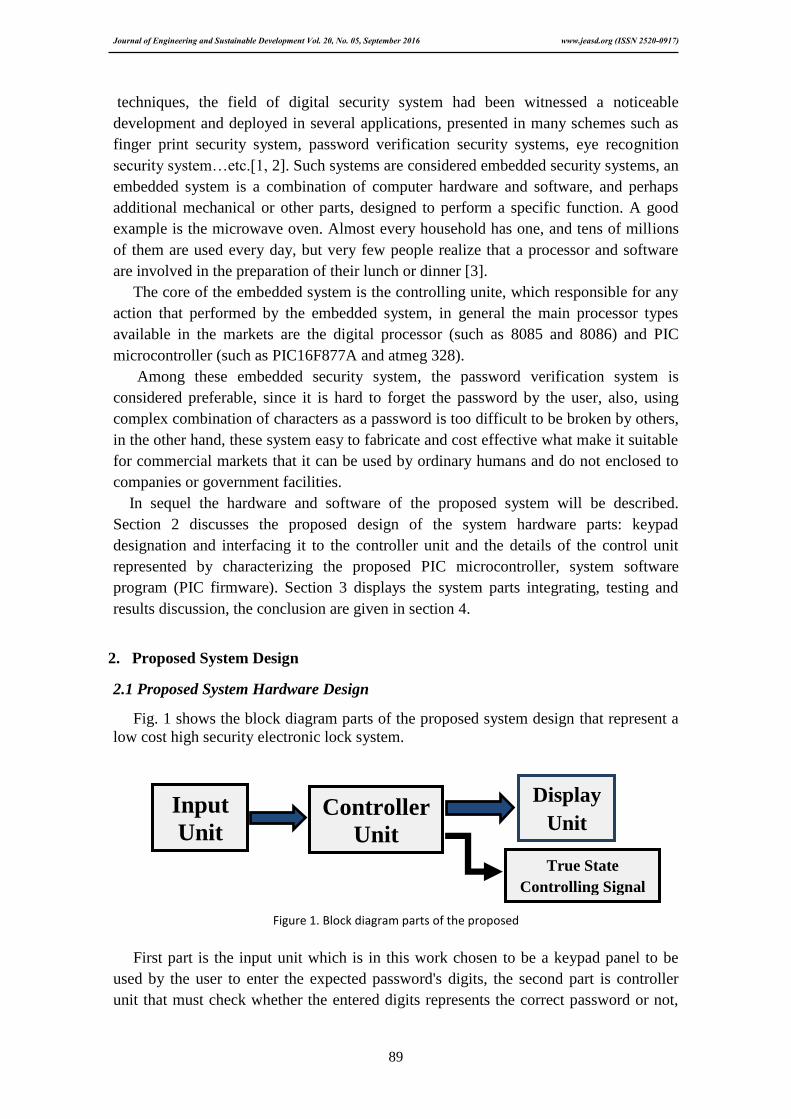
Fig. 1 shows the block diagram parts of the proposed system design that represent a
low cost high security electronic lock system.
Figure 1. Block diagram parts of the proposed
First part is the input unit which is in this work chosen to be a keypad panel to be
used by the user to enter the expected password's digits, the second part is controller
unit that must check whether the entered digits represents the correct password or not,
Input
Unit Controller
Unit
Display
Unit
True State
Controlling Signal
Journal of Engineering and Sustainable Development Vol. 20, No. 05, September 2016 www.jeasd.org (ISSN 2520-0917)
90
the third part is user interactive method explain the instantaneous system state, the
following subsection will discuss the details of hardware and software design
considerations for the proposed system.
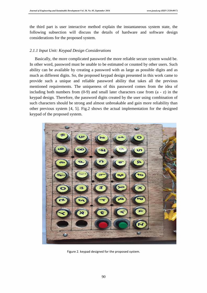
Space with a font size 6 2.1.1 Input Unit: Keypad Design Considerations
Basically, the more complicated password the more reliable secure system would be.
In other word, password must be unable to be estimated or counted by other users. Such
ability can be available by creating a password with as large as possible digits and as
much as different digits. So, the proposed keypad design presented in this work came to
provide such a unique and reliable password ability that takes all the previous
mentioned requirements. The uniqueness of this password comes from the idea of
including both numbers from (0-9) and small later characters case from (a - z) in the
keypad design. Therefore, the password digits created by the user using combination of
such characters should be strong and almost unbreakable and gain more reliability than
other previous system [4, 5]. Fig.2 shows the actual implementation for the designed
keypad of the proposed system.
Figure 2. keypad designed for the proposed system.
Journal of Engineering and Sustainable Development Vol. 20, No. 05, September 2016 www.jeasd.org (ISSN 2520-0917)
91
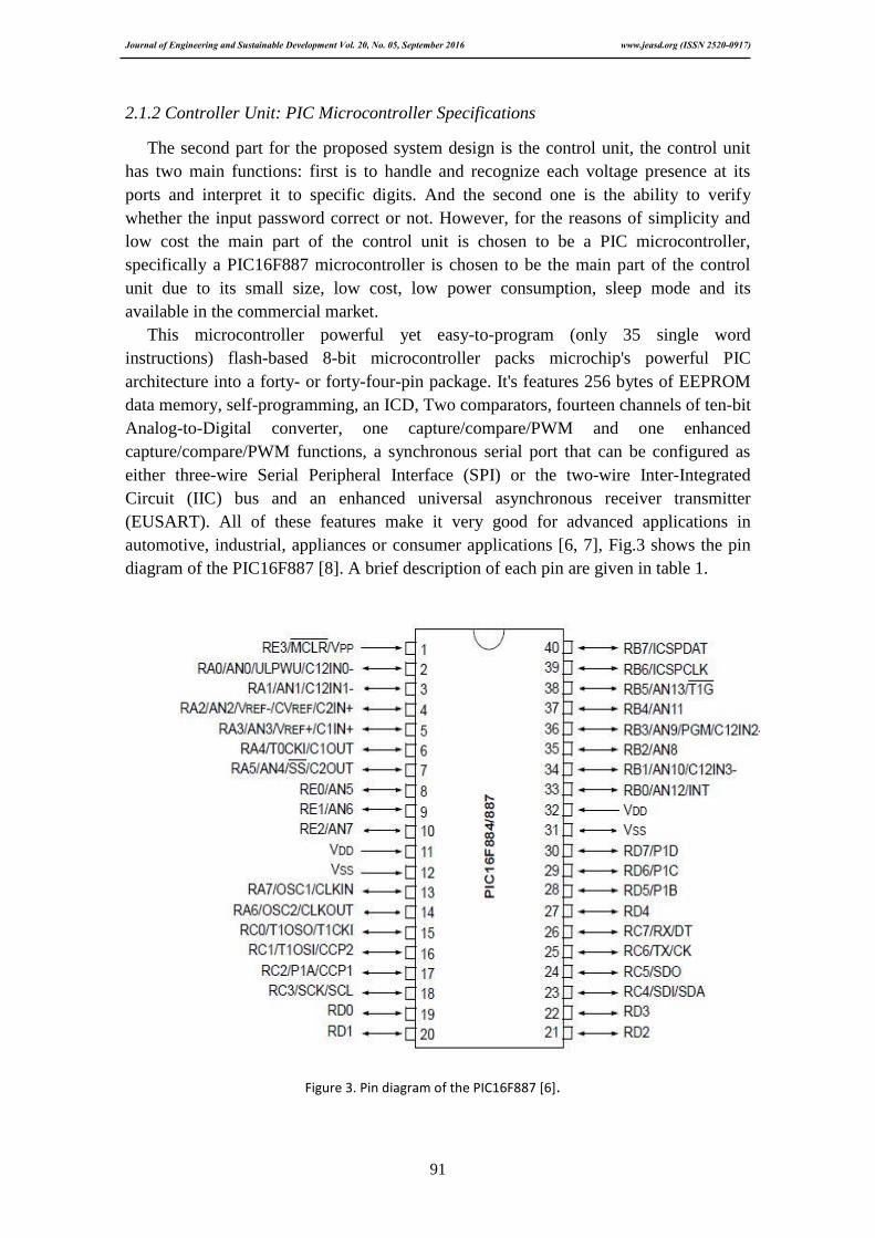
2.1.2 Controller Unit: PIC Microcontroller Specifications
The second part for the proposed system design is the control unit, the control unit
has two main functions: first is to handle and recognize each voltage presence at its
ports and interpret it to specific digits. And the second one is the ability to verify
whether the input password correct or not. However, for the reasons of simplicity and
low cost the main part of the control unit is chosen to be a PIC microcontroller,
specifically a PIC16F887 microcontroller is chosen to be the main part of the control
unit due to its small size, low cost, low power consumption, sleep mode and its
available in the commercial market.
This microcontroller powerful yet easy-to-program (only 35 single word
instructions) flash-based 8-bit microcontroller packs microchip's powerful PIC
architecture into a forty- or forty-four-pin package. It's features 256 bytes of EEPROM
data memory, self-programming, an ICD, Two comparators, fourteen channels of ten-bit
Analog-to-Digital converter, one capture/compare/PWM and one enhanced
capture/compare/PWM functions, a synchronous serial port that can be configured as
either three-wire Serial Peripheral Interface (SPI) or the two-wire Inter-Integrated
Circuit (IIC) bus and an enhanced universal asynchronous receiver transmitter
(EUSART). All of these features make it very good for advanced applications in
automotive, industrial, appliances or consumer applications [6, 7], Fig.3 shows the pin
diagram of the PIC16F887 [8]. A brief description of each pin are given in table 1.
Figure 3. Pin diagram of the PIC16F887 [6].

Journal of Engineering and Sustainable Development Vol. 20, No. 05, September 2016 www.jeasd.org (ISSN 2520-0917)
92
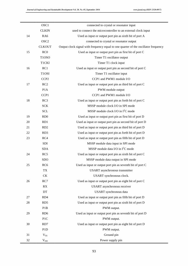
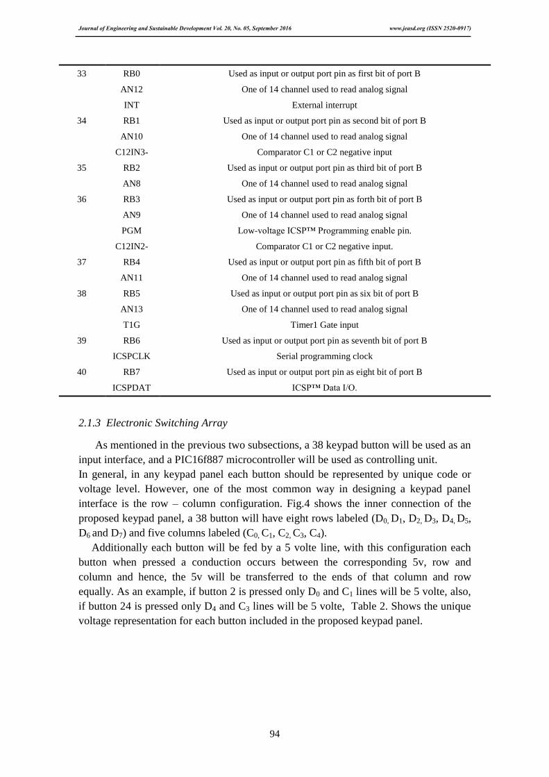
Table 1. General specifications of the PIC16f887 microcontroller [8].
PIN Description PIN
Assignment
PIN
Number
Used as input or output port pin as third bit of port E RE3 1
An active low pin and Stands for Master Clear and can be used to reset the
microcontroller MCLR 1
Programming voltage pin Vpp 1
Used as input or output port pin as first bit of port A RA0 2
Channel 0 which is one of 14 channel used to read analog signal AN0 2
Stands for Ultra Low Power Wake UP used for standby mode deactivation ULPWU 2
Comparator channel 1 or channel 2 negative input C12IN0- 2
Used as input or output port pin as Second bit of port A RA1 3
Channel 1 which is one of 14 channel used to read analog signal AN1 3
Comparator channel 1 or channel 2 negative input C12IN1- 3
Used as input / output port pin as third bit of port A RA2 4
Channel 2 which is one of 14 channel used to read analog signal AN2 4
Analogue to digital convertor negative voltage reference input VREF- 4
Comparator negative voltage reference output CVREF- 4
Comparator C2 positive input C2IN+ 4
Used as input or output port pin as fourth bit of port A RA3 5
Channel 3 which is one of 14 channel used to read analog signal AN3 5
Analogue to digital convertor positive voltage reference input VREF+ 5
Comparator C1 positive input C1IN+ 5
Used as input or output port pin as fifth bit of port A RA4 6
Timer 0 clock signal input pin T0CK1 6
Comparator C1 output C1OUT 6
Used as input or output port pin as sixth bit of port A RA5 7
Channel 4 which is one of 14 channel used to read analog signal AN4 7
Stand foe Slave Select input pin SS 7
Comparator C2 output C2OUT 7
Used as input or output port pin as first bit of port E RE0 8
Channel 5 which is one of 14 channel used to read analog signal AN5 8
Used as input or output port pin as second bit of port E RE1 9
Channel 6 which is one of 14 channel used to read analog signal AN6 9
Used as input or output port pin as third bit of port E RE2 10
Channel 7 which is one of 14 channel used to read analog signal AN7 10
Ground pin VSS 11
Power supply pin VDD 12
Used as input or output port pin as seventh bit of port A RA7 13
Journal of Engineering and Sustainable Development Vol. 20, No. 05, September 2016 www.jeasd.org (ISSN 2520-0917)
93
connected to crystal or resonator input OSC1 13
used to connect the microcontroller to an external clock input CLKIN 13
Used as input or output port pin as sixth bit of port A RA6 14
connected to crystal or resonator output OSC2 14
Output clock signal with frequency equal to one quarter of the oscillator frequency CLKOUT 14
Used as input or output port pin as first bit of port C RC0 15
Timer T1 oscillator output T1OSO 15
Timer T1 clock input T1CKI 15
Used as input or output port pin as second bit of port C RC1 16
Timer T1 oscillator input T1OSI 16
CCP1 and PWM1 module I/O CCP2 16
Used as input or output port pin as third bit of port C RC2 17
PWM module output P1A 17
CCP1 and PWM1 module I/O CCP1 17
Used as input or output port pin as forth bit of port C RC3 18
MSSP module clock I/O in SPI mode SCK 18
MSSP module clock I/O in I2C mode SCL 18
Used as input or output port pin as first bit of port D RD0 19
Used as input or output port pin as second bit of port D RD1 20
Used as input or output port pin as third bit of port D RD2 21
Used as input or output port pin as forth bit of port D RD3 22
Used as input or output port pin as fifth bit of port D RC4 23
MSSP module data input in SPI mode SDI 23
MSSP module data I/O in I2C mode SDA 23
Used as input or output port pin as sixth bit of port C RC5 24
MSSP module data output in SPI mode SDO 24
Used as input or output port pin as seventh bit of port C RC6 25
USART asynchronous transmitter TX 25
USART synchronous clock. CK 25
Used as input or output port pin as eight bit of port C RC7 26
USART asynchronous receiver RX 26
USART synchronous data DT 26
Used as input or output port pin as fifth bit of port D RD4 27
Used as input or output port pin as sixth bit of port D RD5 28
PWM output. P1B 28
Used as input or output port pin as seventh bit of port D RD6 29
PWM output. P1C 29
Used as input or output port pin as eight bit of port D RD7 30
PWM output. P1D 30
Ground pin VSS 31
Power supply pin VDD 32
Journal of Engineering and Sustainable Development Vol. 20, No. 05, September 2016 www.jeasd.org (ISSN 2520-0917)
94
Used as input or output port pin as first bit of port B RB0 33
One of 14 channel used to read analog signal AN12 33
External interrupt INT 33
Used as input or output port pin as second bit of port B RB1 34
One of 14 channel used to read analog signal AN10 34
Comparator C1 or C2 negative input C12IN3- 34
Used as input or output port pin as third bit of port B RB2 35
One of 14 channel used to read analog signal AN8 35
Used as input or output port pin as forth bit of port B RB3 36
One of 14 channel used to read analog signal AN9 36
Low-voltage ICSP™ Programming enable pin. PGM 36
Comparator C1 or C2 negative input. C12IN2- 36
Used as input or output port pin as fifth bit of port B RB4 37
One of 14 channel used to read analog signal AN11 37
Used as input or output port pin as six bit of port B RB5 38
One of 14 channel used to read analog signal AN13 38
Timer1 Gate input T1G 38
Used as input or output port pin as seventh bit of port B RB6 39
Serial programming clock ICSPCLK 39
Used as input or output port pin as eight bit of port B RB7 40
ICSP™ Data I/O. ICSPDAT 40
2.1.3 Electronic Switching Array
As mentioned in the previous two subsections, a 38 keypad button will be used as an
input interface, and a PIC16f887 microcontroller will be used as controlling unit.
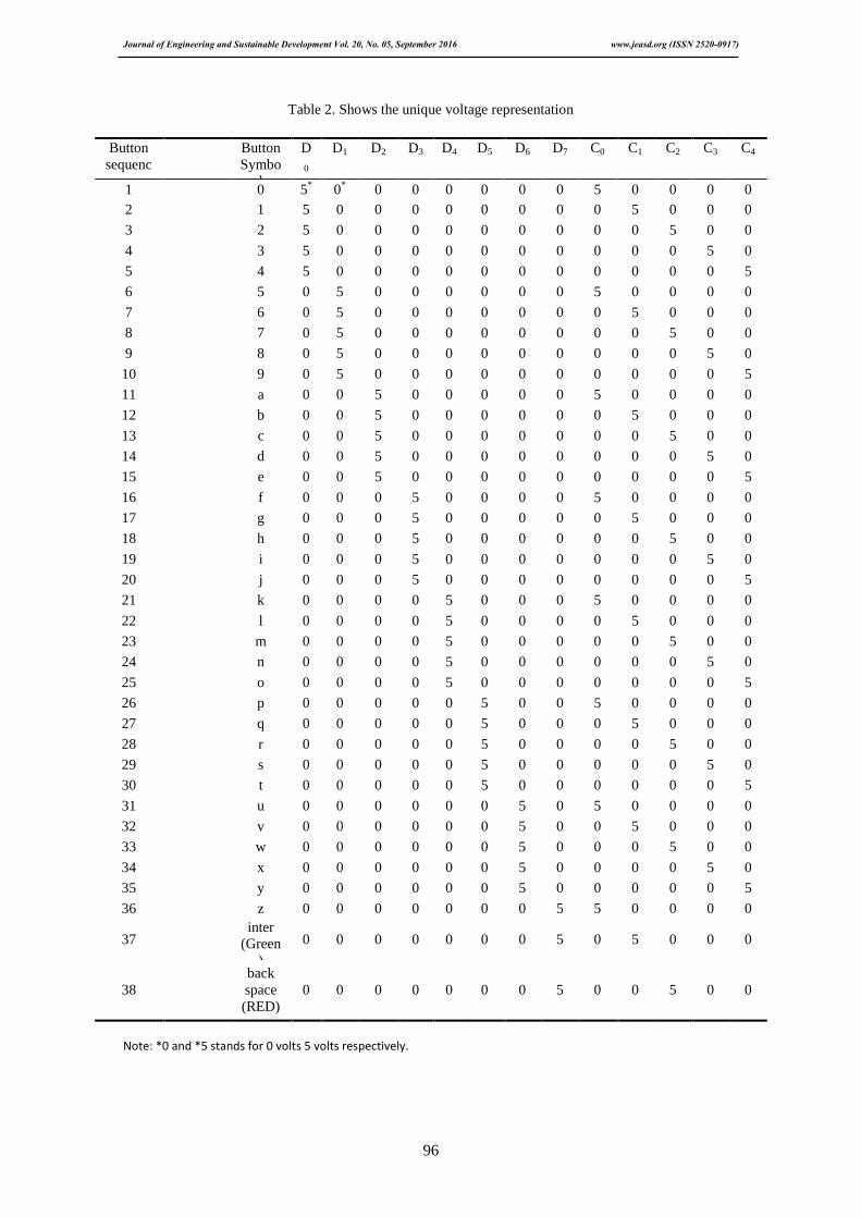
In general, in any keypad panel each button should be represented by unique code or
voltage level. However, one of the most common way in designing a keypad panel
interface is the row – column configuration. Fig.4 shows the inner connection of the
proposed keypad panel, a 38 button will have eight rows labeled (D0, D1, D2, D3, D4, D5,
D6 and D7) and five columns labeled (C0, C1, C2, C3, C4).
Additionally each button will be fed by a 5 volte line, with this configuration each
button when pressed a conduction occurs between the corresponding 5v, row and
column and hence, the 5v will be transferred to the ends of that column and row
equally. As an example, if button 2 is pressed only D0 and C1 lines will be 5 volte, also,
if button 24 is pressed only D4 and C3 lines will be 5 volte, Table 2. Shows the unique
voltage representation for each button included in the proposed keypad panel.

Journal of Engineering and Sustainable Development Vol. 20, No. 05, September 2016 www.jeasd.org (ISSN 2520-0917)
95
Figure 4. Row – Column configuration of the proposed keypad panel.
Button
1
Button
2
Button
3
Button
4
Button
5
Button
6
Button
7
Button
8
Button
9
Button
10
Button
11
Button
12
Button
13
Button
14
Button
15
Button
16
Button
17
Button
18
Button
19
Button
20
Button
26
Button
27
Button
28
Button
29 Button
30
Button
31
Button
32
Button
33
Button
34
Button
35
C0 C1 C2 C3 C4
D0
D1
Button
21
Button
22
Button
23
Button
24
Button
25
5v 5v 5v 5v 5v
5v 5v 5v 5v 5v
5v 5v 5v 5v 5v
5v 5v 5v 5v 5v
5v 5v 5v 5v 5v
5v 5v 5v 5v 5v
5v 5v 5v 5v 5v
Button
36
Button
37
Button
38
5v 5v 5v
D2
D3
D4
D5
D6
D7
Journal of Engineering and Sustainable Development Vol. 20, No. 05, September 2016 www.jeasd.org (ISSN 2520-0917)
96
Table 2. Shows the unique voltage representation
C4 C3 C2 C1 C0 D7 D6 D5 D4 D3 D2 D1 D
0
Button
Symbo
l
Button
sequenc
e 0 0 0 0 5 0 0 0 0 0 0 0
* 5
* 0 1
0 0 0 5 0 0 0 0 0 0 0 0 5 1 2
0 0 5 0 0 0 0 0 0 0 0 0 5 2 3
0 5 0 0 0 0 0 0 0 0 0 0 5 3 4
5 0 0 0 0 0 0 0 0 0 0 0 5 4 5
0 0 0 0 5 0 0 0 0 0 0 5 0 5 6
0 0 0 5 0 0 0 0 0 0 0 5 0 6 7
0 0 5 0 0 0 0 0 0 0 0 5 0 7 8
0 5 0 0 0 0 0 0 0 0 0 5 0 8 9
5 0 0 0 0 0 0 0 0 0 0 5 0 9 10
0 0 0 0 5 0 0 0 0 0 5 0 0 a 11
0 0 0 5 0 0 0 0 0 0 5 0 0 b 12
0 0 5 0 0 0 0 0 0 0 5 0 0 c 13
0 5 0 0 0 0 0 0 0 0 5 0 0 d 14
5 0 0 0 0 0 0 0 0 0 5 0 0 e 15
0 0 0 0 5 0 0 0 0 5 0 0 0 f 16
0 0 0 5 0 0 0 0 0 5 0 0 0 g 17
0 0 5 0 0 0 0 0 0 5 0 0 0 h 18
0 5 0 0 0 0 0 0 0 5 0 0 0 i 19
5 0 0 0 0 0 0 0 0 5 0 0 0 j 20
0 0 0 0 5 0 0 0 5 0 0 0 0 k 21
0 0 0 5 0 0 0 0 5 0 0 0 0 l 22
0 0 5 0 0 0 0 0 5 0 0 0 0 m 23
0 5 0 0 0 0 0 0 5 0 0 0 0 n 24
5 0 0 0 0 0 0 0 5 0 0 0 0 o 25
0 0 0 0 5 0 0 5 0 0 0 0 0 p 26
0 0 0 5 0 0 0 5 0 0 0 0 0 q 27
0 0 5 0 0 0 0 5 0 0 0 0 0 r 28
0 5 0 0 0 0 0 5 0 0 0 0 0 s 29
5 0 0 0 0 0 0 5 0 0 0 0 0 t 30
0 0 0 0 5 0 5 0 0 0 0 0 0 u 31
0 0 0 5 0 0 5 0 0 0 0 0 0 v 32
0 0 5 0 0 0 5 0 0 0 0 0 0 w 33
0 5 0 0 0 0 5 0 0 0 0 0 0 x 34
5 0 0 0 0 0 5 0 0 0 0 0 0 y 35
0 0 0 0 5 5 0 0 0 0 0 0 0 z 36
0 0 0 5 0 5 0 0 0 0 0 0 0 inter
(Green
)
37
0 0 5 0 0 5 0 0 0 0 0 0 0
back
space
(RED)
38
Note: *0 and *5 stands for 0 volts 5 volts respectively.

Journal of Engineering and Sustainable Development Vol. 20, No. 05, September 2016 www.jeasd.org (ISSN 2520-0917)
97
Since all the buttons available in the commercial markets contain two terminals only
a problem rises about how to be able to join the three terminals column, row and five
volte, to overcome this problem transistor configurations functioning as switching
circuit is used, where one pole of the button is connected to the five volte terminal and
the other pole is connected to a two switching transistor circuits as shown in Fig.5
below.
Figure 5. Proposed BJTs Switching Circuit.
When the button is pressed the two transistor will conduct and the 5 volt will
instantly transferred to the corresponding row and column. And since the designed
keypad panel contain a 38 button its required 76 transistor to fulfillment the complete
design. As a result, an electronic switching array based on bipolar junction transistor
(BJT) was designed and implemented, so that each button in the keypad panel when
pressed a crossponding unique presence of input voltages across the pins of the
proposed microcontroller, which in turn programmed to handle such voltage presence
and interpret it to processed for specific task. This BJT array implemented to work only
when the system is activated by the user otherwise it will not consume any power. Fig.6
shows the implementation of the designed BJT switching array. The basic element used
in the design is a C1815 NPN BJT [9].
5 v
To Specific column
To Specific row
Vcc
Vcc
Journal of Engineering and Sustainable Development Vol. 20, No. 05, September 2016 www.jeasd.org (ISSN 2520-0917)
98
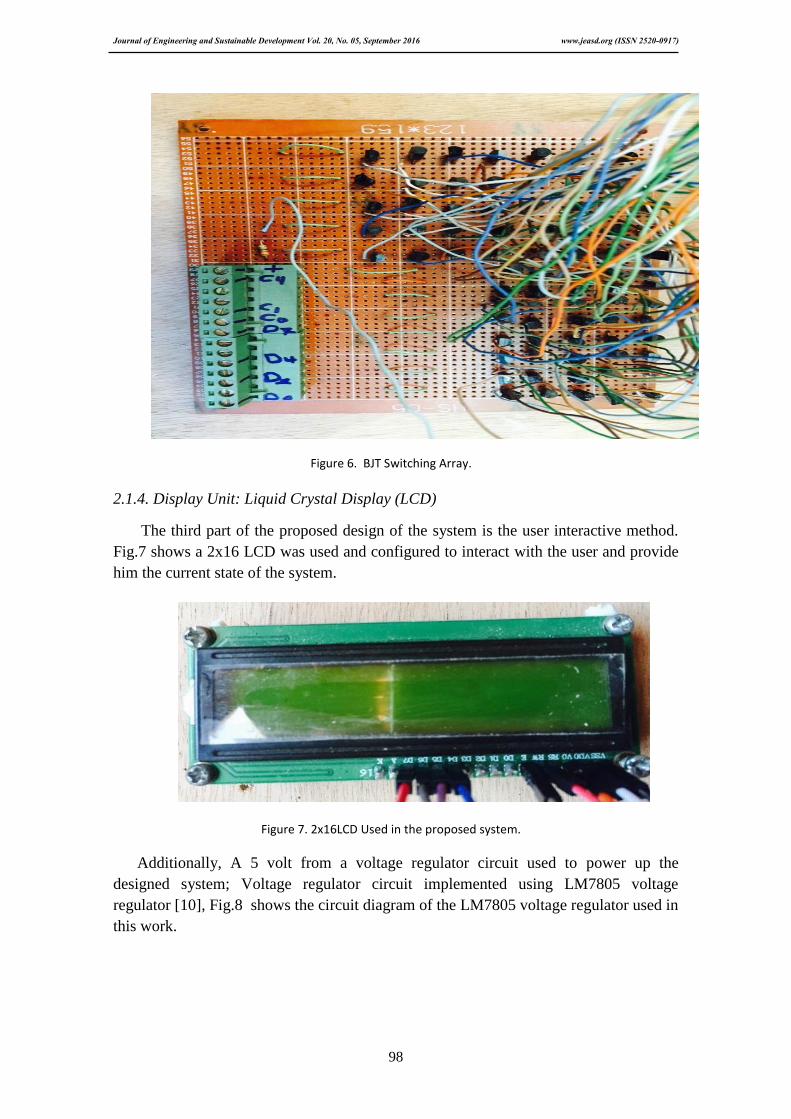
Figure 6. BJT Switching Array.
2.1.4. Display Unit: Liquid Crystal Display (LCD)
The third part of the proposed design of the system is the user interactive method.
Fig.7 shows a 2x16 LCD was used and configured to interact with the user and provide
him the current state of the system.
Figure 7. 2x16LCD Used in the proposed system.
Additionally, A 5 volt from a voltage regulator circuit used to power up the
designed system; Voltage regulator circuit implemented using LM7805 voltage
regulator [10], Fig.8 shows the circuit diagram of the LM7805 voltage regulator used in
this work.

Journal of Engineering and Sustainable Development Vol. 20, No. 05, September 2016 www.jeasd.org (ISSN 2520-0917)
99
Figure 8. LM7805 voltage regulator circuit [10].
2.2 Proposed System Software (PIC Firmware)
The PIC microcontroller program (Firmware) written using micro C environment, in
addition an EasyPic7 trainer board shown in Fig.9 is a PIC microcontroller trainer
which was used for two operations; first one was essential test and second one was
transferring the Intel hex file to the PIC microcontroller chip [6].
Figure 9. EasyPic7 trainer board.
In general, in this work firmware program software can be divided into two main
part; first part is the PIC16F887 microcontroller firmware program that is written to
handle each input unique voltage presence and interpret to a crossponding character or
number, this operation does not depend on the built-in PIC microcontroller standard
keypad library provided by the microcontroller manufacture as in [4, 5], where in this
work, a new whole library is needed and written and a lookup table is made in order to
make the proposed PIC microcontroller able to handle each unique voltage presence and
interpret it to specific unique character.
The second part of the firmware program software is responsible for the main task of
the implemented system, which is password check operation, where, an algorithm is
written to store in sequence each input digits entered by the user via keypad panel
Journal of Engineering and Sustainable Development Vol. 20, No. 05, September 2016 www.jeasd.org (ISSN 2520-0917)
100
interface until the user hits the check button, then this algorithm will check whether the
aggregation of the entered expected password digits perfectly matching the originally
stored correct password or not and perform a specific action corresponding to each state.
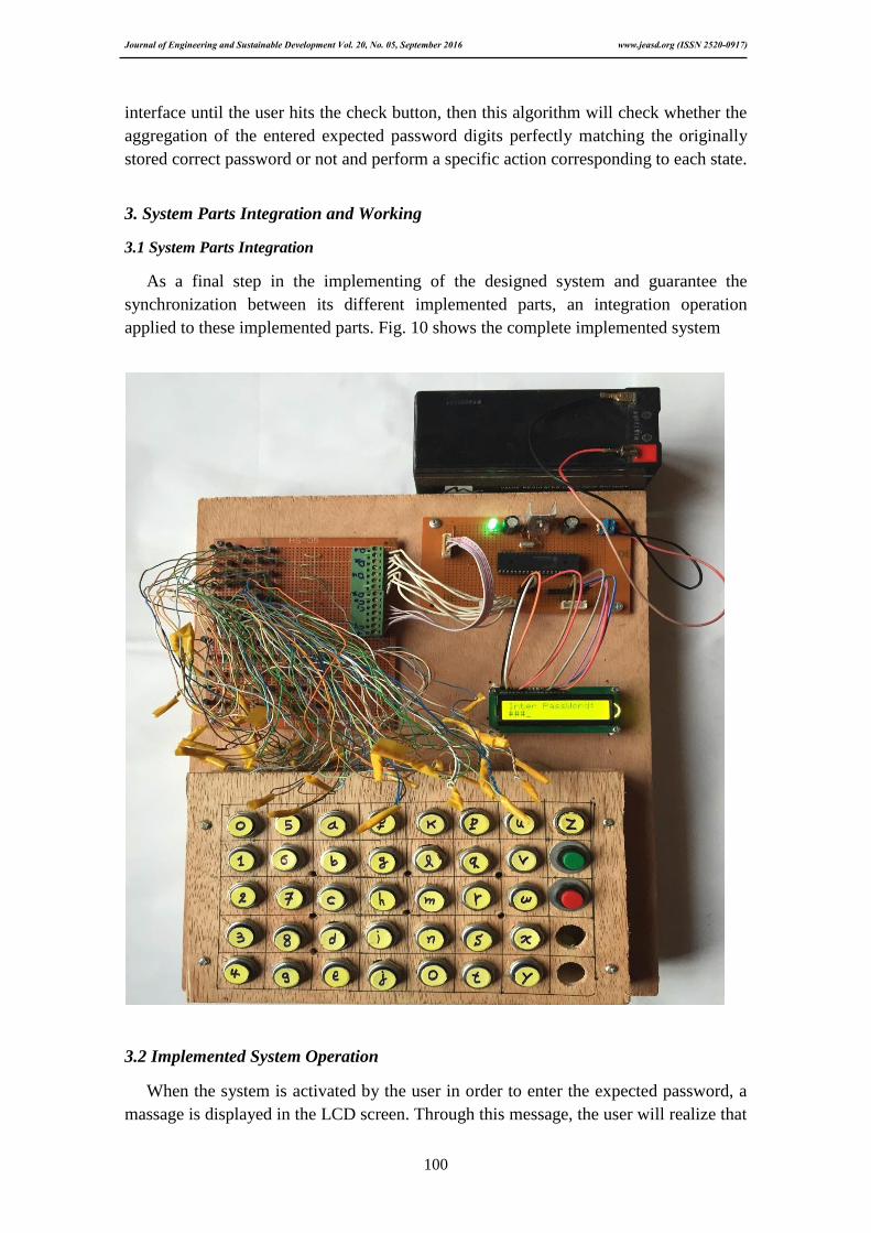
3. System Parts Integration and Working
3.1 System Parts Integration
As a final step in the implementing of the designed system and guarantee the
synchronization between its different implemented parts, an integration operation
applied to these implemented parts. Fig. 10 shows the complete implemented system
3.2 Implemented System Operation
When the system is activated by the user in order to enter the expected password, a
massage is displayed in the LCD screen. Through this message, the user will realize that

Journal of Engineering and Sustainable Development Vol. 20, No. 05, September 2016 www.jeasd.org (ISSN 2520-0917)
101
the system is locked and a password is needed to be unlocked. As the user is entering
the expected password digit by digit via keypad panel, the PIC microcontroller handle
each digit interpret to its crossponding character and stored in sequence order, and
encoded to special symbol " # " to be displayed on the LCD screen to tell the user that a
digit is received and stored as shown in Fig.11.
Figure 11. LCD displaying system status.
when the user complete entering the expected password digits and hits the check
password button to open the system, the microcontroller will check if the aggregation of
the stored entered digits in sequence perfectly match the correct originally stored
password or not and hence, unlock the system or not. If the entered password are true
then a control signal via one of the PORTB pins. In contrast, a rejection message via
LCD screen is displayed to inform the user in case of an incorrect entered password.
It's important to know that in this work, to increase the reliability of the system the
password setting operation done by the system manufacturer only, were the customer
should have a chance to setup his own secret password and then final programming
operation is done for the PIC microcontroller chip. This is mean the password cannot be
set on the field because of the nature work of the PIC microcontroller and It can be reset
through the active low MCLR pin what will make it easy to break up the system by
reset the PIC microcontroller or simply by restarting the system. In both cases and
according to its program it will be forced to ask for the password to be stored, and
hence, a new password can be entered by the 3rd
person and the uses the same password
to unlock the system.
Also, in writing the program algorithm, the number password digits chosen to be six
digits in minimum case and ten digits in maximum case. These numbers can be changed
according to the customer request. However, in this work, since it contains LCD with
maximum row digits to be displayed is sixteen digit, then the maximum number
password digits can be handled by the implemented system is sixteen.
Finally, the user has only three attempts to enter the correct password and bypass the
system otherwise, the system programmed to shut down automatically for desired time
period of twelve hours when the test applied. Also, if the user press more than one
button at the same time the system will not response to such action and stay in its state
without any change.

Journal of Engineering and Sustainable Development Vol. 20, No. 05, September 2016 www.jeasd.org (ISSN 2520-0917)
102
A multiple attempts applied to the implemented system with different passwords, the
response of the implemented system were as expected and no error detected through the
applied test what make the system successfully built and suitable for security
application such as doors, gates, garage and safes.
4. Conclusion
The design and implementation of a cost effective, higher level security electronic
lock based PIC microcontroller was presented in this work. The implemented system
includes a 38 keypad buttons, 16x2 LCD and a PIC16F887 microcontroller. After
integrating the implemented parts of system design, a test is applied and the response is
perfect. However, during the design and implementation the following considerations
were concluded; building physical 38 button keypad and interface it to a such PIC
microcontroller is not easy that is require a specialized knowledge and skills,
additionally, designing an electronic switching array based BJT devices make it
possible to expand the ports of the PIC microcontroller, also, writing and testing the
firmware of the PIC microcontroller shows that it can programmed to perform extra
complex function and not enclosed by simple and basic control operations, and finally,
with good programming abilities such simple, low cost and low power consumption
controller can be used to build system that performs complex task what will lead to
reduce cost and size of that system.
Space with a font
6. References
1. Thomas Norman, (2011). "Electronic Access Control" 1st ed. Butterworth-
Heinemann.
2. Joel Konicek and Karen Little,(1997). "Security, ID Systems and Locks: The Book
on Electronic Access Control" 1st ed., Butterworth-Heinemann;.
3. Michael Barry, (1999)."Programing Embedded Systemsin C and C++" 1st ed.,
O'Reilly.
4. Muhanad H. Mohammed, (2012). Secure Electronic Lock Using PIC16F628A
Microcontroller. International Journal of Research in Computer Science, Vol. 2 No. 5
pp. 43-47.
5. Hamsa F. Thanoon, (2015). "Safetyand Securityofthe PersonalBelongs Using
Microcontroller" Diyala Journal of Engineering Sciences, Vol. 08, No. 02, pp. 28-37.
6. Tim Wilmshurst. (2009). "Designing embedded system with microcontroller
principle and application".2nd
ed.,
7. Lucio Di Jasio … [et al.]. (2007)."PIC Microcontrollers: Know It All", 1sted,Newnes.
8. www.datasheetcatalog.com, "PIC16F PIC16F882/883/884/886/887 data sheet".
9. www.datasheetcatalog.com, "NPN BJT c1815 data sheet".
10. www.datasheetcatalog.com, "BJT LM7805 data sheet".