Design and Implementation of 32 Bit Unsigned Multiplier Using...
5
Design and Implementation of 32 Bit Unsigned Multiplier Using CLAA and CSLA V.Vijayalakshmil, R.Seshadd, Dr.S.Ramakrishnan3 1 , 2 Arunai Engineering College, 3 Sakthi Marianan Engineering College, 1 , 2 Tiruvnamalai, 3 Thandalam, Chennai. I [email protected], 2 [email protected], 3 [email protected] Ahsact-This project deals with the comparison of the VLSI design of the carry look-ahead adder (CLAA) based 32-bit unsigned integer multiplier and the VLSI design of the carry select adder (CSLA) based 32-bit unsigned integer multiplier. Both the VLSI design of multiplier mUltiplies two 32-bit unsigned integer values and gives a product term of 64-bit values. The CLAA based multiplier uses the delay time of 99ns for performing mUltiplication operation where as in CSLA based multiplier also uses nearly the same delay time for mUltiplication operation. But the area needed for CLAA multiplier is reduced to 31 % by the CSLA based multiplier to complete the mUltiplication operation. These multipliers are implemented using Altera Quartus II and timing diagrams are viewed through avan waves. Keywords-CLAA; CSLA; Delay; Area; Array Multiplier; VL Modeling & Simulation. T. I NTRODUCTI ON Digital computer arimetic is an aspect of logic design with the objective of developing appropriate algorims in order to achieve an efficient utilization of the available hardware. The basic operations are addition, subtraction, multiplication and division. In this, we are going to deal with the operation of additions implemented to the operation of multiplication. The repeated form of the addition operations and shiſting results in the multiplication operations. Given that the hardware can only perform a relatively simple and primitive set of Boolean operations, arimetic operations are based on a hierarchy of operations that are built upon the simple ones. In VLSI designs, speed, power and chip area are the most oſten used measures for determining the performance and efficiency of the VLSI architecture. Multiplications and additions are most widely and more oſten used arimetic computations performed in all digital signal processing applications. Addition is a ndamental operation for any digital multiplication. A fast, area efficient and accurate operation of a digital system is greatly influenced by the performance of the resident adders. Adders are also very important component in digital systems because of their extensive use in these systems. In this project we are going to compare the performance of different adders implemented to the multipliers based on area and time needed for calculation. On comparison with the carry look-ahead adder (CLAA) based multiplier the area of calculation of the carry select adder (CSLA) based multiplier is smaller and better with nearly same delay time. Here we are dealing with the comparison in the bit range of n*n (32*32) as input and 2n (64) bit output. Hence, to design a better architecture the basic adder blocks must have reduced delay time consumption and area efficient architectures. The demand is of DSP style systems for both less delay time and less area requirement for designing the systems. Our interest is in the basic building blocks of arithmetic circuits that dominate in DSP applications, VLSI architectures, computer applications and where ever reduced area computation is needed. IT. CARRY LOOK-AHEAD ADDER Carry Look Ahead Adder can produce carries faster due to parallel generation of the carry bits by using additional circuiy. This technique uses calculation of carry signals in advance, based on input signals. The result is reduced carry propagation time. For example, ripple adders are slower but use the least energy. Figurel. Carry Look-Ahead Adder 978-1-4673-5301-4/13/$31.00 ©2013 EE
Transcript of Design and Implementation of 32 Bit Unsigned Multiplier Using...

Design and Implementation of 32 Bit Unsigned
Multiplier Using CLAA and CSLA
V.Vijayalakshmil, R.Seshadd, Dr.S.Ramakrishnan3 1,2 Arunai Engineering College,
3 Sakthi Mariannnan Engineering College,
1,2Tiruvannamalai, 3Thandalam, Chennai.
[email protected], [email protected]
Ahstract-This project deals with the comparison of the VLSI design of the carry look-ahead adder (CLAA) based 32-bit unsigned integer multiplier and the VLSI design of the carry
select adder (CSLA) based 32-bit unsigned integer multiplier. Both the VLSI design of multiplier mUltiplies two 32-bit unsigned integer values and gives a product term of 64-bit values. The CLAA based multiplier uses the delay time of 99ns for performing mUltiplication operation where as in CSLA based multiplier also uses nearly the same delay time for mUltiplication operation. But the area needed for CLAA multiplier is reduced to 31 % by the CSLA based multiplier to
complete the mUltiplication operation. These multipliers are implemented using Altera Quartus II and timing diagrams are viewed through avan waves.
Keywords-CLAA; CSLA; Delay; Area; Array Multiplier; VHDL Modeling & Simulation.
T. INTRODUCTION
Digital computer arithmetic is an aspect of logic
design with the objective of developing appropriate
algorithms in order to achieve an efficient utilization of the
available hardware. The basic operations are addition,
subtraction, multiplication and division. In this, we are going
to deal with the operation of additions implemented to the
operation of multiplication. The repeated form of the
addition operations and shifting results in the multiplication
operations.
Given that the hardware can only perform a
relatively simple and primitive set of Boolean operations,
arithmetic operations are based on a hierarchy of operations
that are built upon the simple ones. In VLSI designs, speed,
power and chip area are the most often used measures for
determining the performance and efficiency of the VLSI
architecture.
Multiplications and additions are most widely and
more often used arithmetic computations performed in all
digital signal processing applications. Addition is a
fundamental operation for any digital multiplication. A fast,
area efficient and accurate operation of a digital system is
greatly influenced by the performance of the resident adders.
Adders are also very important component in digital systems
because of their extensive use in these systems.
In this project we are going to compare the
performance of different adders implemented to the
multipliers based on area and time needed for calculation.
On comparison with the carry look-ahead adder (CLAA)
based multiplier the area of calculation of the carry select
adder (CSLA) based multiplier is smaller and better with
nearly same delay time. Here we are dealing with the
comparison in the bit range of n*n (32*32) as input and 2n
(64) bit output.
Hence, to design a better architecture the basic
adder blocks must have reduced delay time consumption and
area efficient architectures. The demand is of DSP style
systems for both less delay time and less area requirement
for designing the systems. Our interest is in the basic
building blocks of arithmetic circuits that dominate in DSP
applications, VLSI architectures, computer applications and
where ever reduced area computation is needed.
IT. CARRY LOOK-AHEAD ADDER
Carry Look Ahead Adder can produce carries faster
due to parallel generation of the carry bits by using
additional circuitry. This technique uses calculation of carry
signals in advance, based on input signals. The result is
reduced carry propagation time. For example, ripple adders
are slower but use the least energy.
Figurel. Carry Look-Ahead Adder
978-1-4673-5301-4/13/$31.00 ©2013 IEEE

Let Gi is the carry generate function and Pi be the
carry propagate function, Then we can rewrite the carry
function as follows:
Gi = Ai· Bi.
Pi = (Ai xor Bi).
Si = Pi xor Ci.
Ci+l= Gi + Pi.Ci.
(1)
(2)
(3)
(4)
Thus, for 4-bit adder, we can compute the carry for
all the stages as shown below:
C1 = Go + Po.Co. (5)
C2 = G1 + P1.C1 = G1 + P1.GO + P1.PO.CO (6)
C3 = G2 + P2.C2 = G2 + P2.G1 + P2.P I.GO
+ P2.P1.PO.CO (7) C4 = G3 + P3.C3 = G3 + P3.G2 + P3.P2 .G1 + P3.P2.P1.GO
+ P3.P2.Pl.PO.CO (8)
In general, we can write:
The sum function:
In general, we can write the algorithm as:
If Carry in =1, then the sum and carry out are given by,
Sum (i) =a (i) xor b (i) xor '1'. (11)
Carry (i+ 1) = (a (i) and b (i)) or (b (i) or a (i)). (12)
If Carry in =0, then the sum and carry out are given by,
The sum function:
Sum (i) = a (i) xor b (i).
Carry (i+ 1) = (a (i) and b (i)).
The carry function:
IV. MUL TIPLTER FOR UNSIGNED DATA
(13)
(14)
(IS)
(16)
(9) Multiplication involves the generation of partial
The carry function:
Ci+l= Gi + Pi.Ci. (10)
TTL CARRY SELECT ADDER
The concept of CSLA is to compute alternative
results in parallel and subsequently selecting the correct
result with single or multiple stage hierarchical techniques.
In CSLA both sum and carry bits are calculated for two
alternatives Cin=O and 1. Once Cin is delivered, the correct
computation is chosen using a mux to produce the desired
output. Instead of waiting for Cin to calculate the sum, the
sum is correctly output as soon as Cin gets there. The time
taken to compute the sum is then avoided which results in
good improvement in speed.
Cin
S7:4 5:3:0
Figure2. Carry Select Adder
products, one for each digit in the multiplier, as in
Figure3.These partial products are then summed to produce
the final product. The multiplication of two n-bit binary
integers results in a product of up to 2n bits in length [2].
b (0)
b (1)
b (2)
b (31)
32
roj(63 downto 32) prod(31 ) [lrod(O)
Figure3. A partial schematic ofthe multiplier
We used the following algorithm to implement the
multiplication operation for unsigned data.
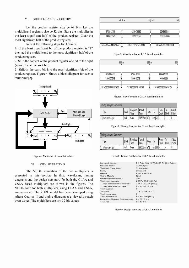
v. MULTIPLICATION ALGORITHM
Let the product register size be 64 bits. Let the
multiplicand registers size be 32 bits. Store the multiplier in
the least significant half of the product register. Clear the
most significant half of the product register.
Repeat the following steps for 32 times:
1. If the least significant bit of the product register is "1"
then add the multiplicand to the most significant half of the
product register.
2. Shift the content of the product register one bit to the right
(ignore the shifted-out bit.)
3. Shift-in the carry bit into the most significant bit of the
product register. Figure 4.Shows a block diagram for such a
multiplier [2].
Multiplicand
Shll'land Add Con 11'01 Lugie
Figure4. Multiplier of two n-bit values.
VI. VHDL SIMULATIONS
The VHDL simulation of the two multipliers is
presented in this section. Tn this, waveforms, timing
diagrams and the design summary for both the CLAA and
CSLA based multipliers are shown in the figures. The
VHDL code for both multipliers, using CLAA and CSLA,
are generated. The VHDL model has been developed using
Altera Quartus IT and timing diagrams are viewed through
avan waves. The multipliers use two 32-bit values.
40.0ns 500ns 601 I I I
3782682799 X 4230476960 1 3048485111 ) 1404927549 X 1699019376 1 1908060884 )
5314395273443529651 X 7187662324761576960 + 5816695195755493124 )
FigureS. Waveform for a CLAA based multiplier
40.0ns 5O.0ns 601 I I
3782682799 1 4230476S60 X 3048485111
1404927549 1699019376 X 1908060884
5314395273443529651 t 7187662324761576960 X 5816695195755493124
Figure6. Waveform for a CSLA based multiplier
Timing Analyzer Summary
Type Slack .. .
1 Worst·case t� �/A
ReqJred I�� If IT Time Tine rom 0
from
ITo
C� Cb:k
Nooe T9Il.5b5 �a[3] -"-lIl{S:3] .. }
Figure7. Timing Analysis for CLAA based multiplier
Timing Analyzer Summary
Type Slack Required Actual
From To From To
Time Time Clock Clock
I Worst·case tpd NIA None 99.553 m all] suml63] .. ..
FigureS. Timing Analysis for CSLA based multiplier
F��d P�tm
0
Failed Paths
0
Quartus II Version
Revision Name
8.1 Build 163 1012812008 SJ Web Ed�ion
CLAmuttiplier
Top-level Entrty Name CLAmultiplier
Family Cyclone II
Device EP=35F672C6
Timing Models Rnal
Met timing requirements Yes
Total logic elements 2.957/33.216 (9 %)
Total combinational functions 2.957 I 33.216 (9 %)
Dedicated logic registers 0 / 33.216 ( 0 % )
Total registers 0
Total pins 129 / 475 (27 %)
Total virtual pins 0
Total memory b�s 0/48.3.840 (0 %)
Embedded Multiplier 9-bit elements 0 / 70 ( 0 % )
Total PLLs 0/4(0%)
Figure9. Design summary ofCLAA multiplier
I
j.

Quartus II Version
Revision Name
T op�evel Entity Name
Family
Device
Timing Models
8.1 Build 163 1012812008 SJ Web Ed�ion
cs amultiplier
csamultiplier
Cyclone II
EP2C35F672C6
Rnal
Met timing requirements Yes
Total logic elements 2,039/33.216 (6'4)
Total combinational functions 2,03:9 / 3.3.216 ( 6 +4 )
Dedicated logic registers 0 / 3.3.216 ( 0 % )
Total registers 0
Total pins 129/475 ( 27 %)
Total virtual pins 0
Total memory b�s 0 1 483,840 ( 0 "'. )
Embedded Mu�iplier 9-b� elements 0 I 70 ( 0 '4 )
Total PLLs 0/4(0%)
FigurelO, Design summary ofCSLA multiplier
Under the worst case, the multiplier with a carry
look-ahead adder uses time = 98.5 ns, while the multiplier
with the carry select adder uses time = 99.5 ns.
VII, PERFORMANCE ANALYSTS
A. Area Analysis
The performance analysis for the area of CLAA and
CSLA based multipliers are represented in the form of the
diagram shown in figure II.
Figure I I , Area analysis chart
B. Delay Analysis
The performance analysis for the delay time of
CLAA and CSLA based multipliers are represented in the
form of the diagram shown in figure 12.
CLAA CSLA
Figure I 2, Delay analysis chart
C.Area Delay Product Analysis
The performance analysis for the area delay product
of CLAA and CSLA based multipliers are represented in the
form of the diagram shown in figure13.
CLAA
Figure I 3, Area delay product analysis chart
The area needed and delay for both the CLAA and
CSLA implemented to the multiplier was analyzed and the
comparison was shown in the figure 14 in the form of a table.
D.Analysis Table
Tn this analysis table shown in figurel4, the delay
time is nearly same, the area and the area delay product of
CSLA based multiplier is reduced to 31 % when compared to
CLAA based multiplier.

Figurel4. Analysis Table
Multiplier type Delay Delay Area Area
(ns) Product
CLAA based 2957
multiplier 98. 5 logic 291264.5
cells
CSLA based 2039
multiplier 99. 5 logic 202880.5
cells
VITI. CONCLUSION
A design and implementation of a VHDL-based 32-
bit unsigned multiplier with CLAA and CSLA was
presented. VHDL, a Very High Speed Integrated Circuit
Hardware Description Language, was used to model and
simulate our multiplier. Using CSLA improves the overall
performance of the multiplier.
Thus a 31 % area delay product reduction is
possible with the use of the CSLA based 32 bit unsigned
parallel multiplier than CLAA based 32 bit unsigned parallel
multiplier.
IX. FUTURE WORK
This 32 bit multiplier can be further extended to 64
bit multiplier and 128 bit multiplier using the proposed
method for multiplication operation can be done as future
work.
REFERENCES
[I] P. Asadi and K. Navi, "A novel highs-speed 54-54 bit multiplier", Am. J Applied Sci., vol. 4 (9), pp. 666-672. 2007.
[2] W. Stallings, Computer Organization and Architecture Designing for
Peljormance, 71h ed., Prentice Hall, Pearson Education International, USA, 2006, ISBN: 0-13-185644-8.
[3] 1. F. Wakerly, Digital Design-Principles and Practices, 4th ed. , Pearson Prentice Hall, USA, 2006. ISBN: 0131733494.
[4] A. Sertbas and R.S. Ozbey, "A performance analysis of classified binary adder architectures and the VHDL simulations", J Elect.
Electron. Eng., Istanbul, Turkey, vol. 4, pp. 1025-1030,2004.
[5] P. S. Mohanty, "Design and Implementation of Faster and Low Power Multipliers", Bachelor Thesis. National Institute of Technology, Rourkela, 2009.
[6] S. Brown and Z. Vranesic, Fundamentals of Digital Logic with VHDL
Design, 2nd ed. , McGraw-Hill Higher Education, USA, 2005. ISBN: 0072499389.
[7] J. R. Armstrong and F.G. Gray, VHDL Design Representation and
Synthesis, 2nd ed. , Prentice Hall, USA, 2000. ISBN: 0-13-021670-4.
[8] Z. Navabi, VHDL Modular Design and Synthesis of Cores and
Systems, 3rd ed. , McGraw-Hill Professional, USA, 2007. ISBN: 9780071508926.
[9] P. C. H. Meier, R. A. Rutenbar and L. R. Carley, "Exploring
Multiplier Architecture and Layout for low Power", CIC'96, 1996.
[10] Software Simulation Package: Direct VHDL, Version 1.2, 2007, Green Mounting Computing Systems, Inc., Essex, VT, UK.
[II] Hasan Krad and Aws Yousi( "Design and Implementation of a Fast Unsigned 32-bit Multiplier Using VHDL", 20 I O.
Dr.S.Ramakrishnan was born in Tirunelveli, India in 1969. He received his Bachelors of Engineering degree fi'om the deprniment of Electronics and Instrumentation fi'om Annamalai University, Chidambaram, India and Masters Degree & Ph.D in Electrical
Engineering fi'om Anna University, Chennai India. He has over 15 years of teaching experience after 5 years experience in the industry. He is currently working as Principal & HeadlDeprniment of IT in Sakthi MrnTiamman Engineering College, Chennai, India.He is the member of IEEE & IETE. He has published in many peer refelTed international and national journals and conferences.
Mr.R.Seshadri received the B.E and M.E degrees, both in Electronics and communication engineering fi'om the S.K.P Engineering College, Tiruvannamalai, Tamilnadu, India. He has doing the Ph.D degree in Digital Signal Processing Architecture at Anna University, India. Currently, he is working as a Assistant
Professor in Arunai Engineering College, Tiruvannamalai, Tamilnadu, India. He has having 4 years of teaching Experience.
V.Vijayalakshmi was born on October 12, 1990 in
Tiruvannamalai, Tamilnadu, India. She has received the B.E degree in Electrical and Electronics Engineering from Arunai College of Engineering, Anna University, Chennai, Tamilnadu, India, in May 2011. She is currently pursuing her M.E degree in Applied Electronics fi'om Arunai Engineering College, Anna University, Chennai, Tamilnadu, India from 2011 to 2013. She has published a journal in National conference conducted by Sri Balaji Chockalingam Engineering College on January, 2013. Her areas of
interest include VLSI and Control Systems.

![OpenGL 4.3 API Reference Card Page 1 · OpenGL 4.3 API Reference Card Page 1 OpenGL Operation Floating-Point Numbers [2.3.3] 16-Bit 1-bit sign, 5-bit exponent, 10-bit mantissa Unsigned](https://static.fdocuments.in/doc/165x107/601446bff9d8373bea23177c/opengl-43-api-reference-card-page-1-opengl-43-api-reference-card-page-1-opengl.jpg)