Design and Implementation 4-Bit Quaternary MVL Arithmetic ...
9
330 Technical Gazette 25, Suppl. 2(2018), 330-338 ISSN 1330-3651 (Print), ISSN 1848-6339 (Online) https://doi.org/10.17559/TV-20170210143503 Original scientific paper Design and Implementation 4-Bit Quaternary MVL Arithmetic and Logic Unit Wissam ALJANABI, Mehmet ALBAYRAK Abstract: In the recent years, there were major importance to Multiple Valued Logic (MVL), where the most common reasons for considering the implementation of MVL circuits better then binary valued circuits are that reducing wiring congestion as compared to binary circuits, using a single conductor to transmit three or more discrete voltage or current values allows for greater information content per wire and the circuit cost models would be more economical. Therefore, in this paper the MVL concepts have been used to design 4-bit quaternary MVL Arithmetic and Logic Unit, which is considered a basic unit of a MVL microprocessor. It is the "heart" of a microprocessor and we could say that everything else in the microprocessor is there to support the ALU. The proposed Arithmetic and Logic Unit will do the operations as Addition, Subtraction, Maximum, Minimum and Invert. Simulation Program with Integrated Circuit Emphasis (SPICE) tool in Cadence simulator used in simulation the proposed Arithmetic and Logic Unit. The simulation results tells that the design is more efficient compared with the binary ALU and the circuit will be less area and less number of transistors. Keywords: Current Mode Logic; full adder; full subtractor; MVL (Multiple Valued Logic); MVL ALU (Multiple Valued Logic Arithmetic and Logic Unit) 1 INTRODUCTION Multiple Valued Logic (MVL) or Many-Valued Logic (in some references) is a discrete p-valued system where p > 2, or in other words, non-binary valued system [1]. In MVL, the number of discrete logic levels is not confined to two. This is unlike binary, which only has two levels, logic level 0 and logic level 1, but discrete variables with an infinite number of values can be considered as MVL [2]. MVL has many useful applications and it has been used in design of electronic circuits, which employ more than two discrete levels of signals such as multiple-valued memories, multiple-valued arithmetic circuits, Field Programmable Gate Arrays etc. Multiple valued logic circuits can be designed in Current-mode, Voltage-mode and Mixed-mode. Due to the limited supply voltages, higher radices cannot be obtained using voltage mode circuits. On the other hand, current mode circuits have the advantages of current scaling, copying and sign changing with a simple current mirror, but unlike binary logic circuits, they are not self-restoring. Thus, in this work current mode has been used to design MVL arithmetic and logic unit. In the current mode realization the data are interpreted and transferred by distinct current levels, that are integer multiples of a reference current Ir. The primary rewards of this realization are: 1) Allowing higher radix realization rather than voltage mode circuits. 2) Have larger static power consumption. 3) No need for supplementary circuit for the addition operations. Only we need to collect the wires together. 4) Current fashion is easy for replication or copying, scaling and algebraically sign-change with a simple current mirror circuit [3]. Several factors have influence in deciding the best radix usable. Obviously, in MVL, higher radix would be best to represent as many numbers as possible. However, in practice Quaternary numeral system has many advantages. Quaternary is the base-4 numeral system. It uses the digits 0, 1, 2 and 3 to represent any real number. As with the octal and hexadecimal numeral systems, quaternary has a special relation to the binary numeral system. Each radix 4, 8 and 16 is a power of 2, so the conversion to and from binary is implemented by matching each digit with 2, 3 or 4 binary digits, or bits [4]. The main advantage of Quaternary logic is that it reduces the number of required computation steps for developing digital design leading to increase computational ability. Quaternary logic also offers greater utilization of communication lines because of the higher information content carried by every line. Quaternary logic is a promising alternative for the complex binary circuit as it will reduce the circuit area and circuit cost and power efficiency at the same time. Despite all these advantages, the MVL implementation is still a challenge for the researchers because it is not standardized and is not easy, so the realization of some functions is easy and the others is complex. The successful MVL should have less logical gates, be capable of realizing with a smaller number of transistors as much as possible and can be narrowed in VLSI technologies. Therefore, the aim of this work is to design the MVL ALU with only three MVL current mode elements. Organization of paper is as follows: section 2 presents the motivation, section 3 contains the related works, and section 4 presents elements of MVL Implementation. The design of quaternary MVL arithmetic and logic unit is presented in section 5, Section 6 contains Current-mode Realization of MVL arithmetic and logic unit. Then we provide our conclusions in Section 7. 2 MOTIVATION The major challenges in VLSI design are reducing the area of chip and increasing speed of the circuit. The traditional binary logic faced many problems nowadays such as routing, speed, the number of instructions, power dissipation and silicon area, in addition to the increasing of the number of transistors according to Moore’s law [5]. The widespread use of binary logic was due to their simple realization by available relays, vacuum tube, diodes, and final transistors [6]. The new microprocessor fabrication needs about 10 9 transistors while the number of connections is approximately 10 11 [7]. The engineering
Transcript of Design and Implementation 4-Bit Quaternary MVL Arithmetic ...
330 Technical Gazette 25, Suppl. 2(2018), 330-338
ISSN 1330-3651 (Print), ISSN 1848-6339 (Online) https://doi.org/10.17559/TV-20170210143503 Original scientific paper
Design and Implementation 4-Bit Quaternary MVL Arithmetic and Logic Unit
Wissam ALJANABI, Mehmet ALBAYRAK
Abstract: In the recent years, there were major importance to Multiple Valued Logic (MVL), where the most common reasons for considering the implementation of MVL circuits better then binary valued circuits are that reducing wiring congestion as compared to binary circuits, using a single conductor to transmit three or more discrete voltage or current values allows for greater information content per wire and the circuit cost models would be more economical. Therefore, in this paper the MVL concepts have been used to design 4-bit quaternary MVL Arithmetic and Logic Unit, which is considered a basic unit of a MVL microprocessor. It is the "heart" of a microprocessor and we could say that everything else in the microprocessor is there to support the ALU. The proposed Arithmetic and Logic Unit will do the operations as Addition, Subtraction, Maximum, Minimum and Invert. Simulation Program with Integrated Circuit Emphasis (SPICE) tool in Cadence simulator used in simulation the proposed Arithmetic and Logic Unit. The simulation results tells that the design is more efficient compared with the binary ALU and the circuit will be less area and less number of transistors. Keywords: Current Mode Logic; full adder; full subtractor; MVL (Multiple Valued Logic); MVL ALU (Multiple Valued Logic Arithmetic and Logic Unit) 1 INTRODUCTION
Multiple Valued Logic (MVL) or Many-Valued Logic (in some references) is a discrete p-valued system where p > 2, or in other words, non-binary valued system [1]. In MVL, the number of discrete logic levels is not confined to two. This is unlike binary, which only has two levels, logic level 0 and logic level 1, but discrete variables with an infinite number of values can be considered as MVL [2]. MVL has many useful applications and it has been used in design of electronic circuits, which employ more than two discrete levels of signals such as multiple-valued memories, multiple-valued arithmetic circuits, Field Programmable Gate Arrays etc.
Multiple valued logic circuits can be designed in Current-mode, Voltage-mode and Mixed-mode. Due to the limited supply voltages, higher radices cannot be obtained using voltage mode circuits. On the other hand, current mode circuits have the advantages of current scaling, copying and sign changing with a simple current mirror, but unlike binary logic circuits, they are not self-restoring. Thus, in this work current mode has been used to design MVL arithmetic and logic unit. In the current mode realization the data are interpreted and transferred by distinct current levels, that are integer multiples of a reference current Ir. The primary rewards of this realization are: 1) Allowing higher radix realization rather than voltage
mode circuits. 2) Have larger static power consumption. 3) No need for supplementary circuit for the addition
operations. Only we need to collect the wires together. 4) Current fashion is easy for replication or copying,
scaling and algebraically sign-change with a simple current mirror circuit [3]. Several factors have influence in deciding the best
radix usable. Obviously, in MVL, higher radix would be best to represent as many numbers as possible. However, in practice Quaternary numeral system has many advantages. Quaternary is the base-4 numeral system. It uses the digits 0, 1, 2 and 3 to represent any real number. As with the octal and hexadecimal numeral systems,
quaternary has a special relation to the binary numeral system. Each radix 4, 8 and 16 is a power of 2, so the conversion to and from binary is implemented by matching each digit with 2, 3 or 4 binary digits, or bits [4].
The main advantage of Quaternary logic is that it reduces the number of required computation steps for developing digital design leading to increase computational ability. Quaternary logic also offers greater utilization of communication lines because of the higher information content carried by every line. Quaternary logic is a promising alternative for the complex binary circuit as it will reduce the circuit area and circuit cost and power efficiency at the same time.
Despite all these advantages, the MVL implementation is still a challenge for the researchers because it is not standardized and is not easy, so the realization of some functions is easy and the others is complex. The successful MVL should have less logical gates, be capable of realizing with a smaller number of transistors as much as possible and can be narrowed in VLSI technologies. Therefore, the aim of this work is to design the MVL ALU with only three MVL current mode elements.
Organization of paper is as follows: section 2 presents the motivation, section 3 contains the related works, and section 4 presents elements of MVL Implementation. The design of quaternary MVL arithmetic and logic unit is presented in section 5, Section 6 contains Current-mode Realization of MVL arithmetic and logic unit. Then we provide our conclusions in Section 7.
2 MOTIVATION
The major challenges in VLSI design are reducing the area of chip and increasing speed of the circuit. The traditional binary logic faced many problems nowadays such as routing, speed, the number of instructions, power dissipation and silicon area, in addition to the increasing of the number of transistors according to Moore’s law [5].
The widespread use of binary logic was due to their simple realization by available relays, vacuum tube, diodes, and final transistors [6]. The new microprocessor fabrication needs about 109 transistors while the number of connections is approximately 1011 [7]. The engineering
Wissam ALJANABI, Mehmet ALBAYRAK: Design and Implementation 4-Bit Quaternary MVL Arithmetic and Logic Unit
Tehnički vjesnik 25, Suppl. 2(2018), 330-338 331
viewpoint can easily lead to the number of connections is 100 more than the number of transistors. Thus, this will bring that the silicon region of active elements less than the silicon area of the passive elements. That great problem is being raised a new challenge starting from power consumption to the routing complexity [8].
To overcome the above limitations in binary systems realization and fabrication, the solutions may portion into two main parts: 1) Hardware solutions (circuit level). 2) Software solutions (computer-based solutions).
The hardware solutions taken many considerations like
the decreasing number of transistors [5], changing the realization from voltage mode to the current mode [8], pipeline technologies [9] and finally they tried to move from binary to fully multi-valued logic [10].
The software solutions take the minimization of algorithms for arithmetic operations [11]. Developing simulation algebra for gate level logic circuits that used for analyzing and simulated transients, errors, unknown and states in the binary logic [12].
For all the above problems MVL, appear as a real solution, which may be indispensable for the realization of integrated circuits in the near future. 3 RELATED WORK
According to paper [13] present a full adder prototype based on the designed LUT, fictitious in a standard 130-nm CMOS technology, able to work at 100 MHz while overriding 122 μW. The experimental results express the correct quaternary operation and confirm the power efficiency of the proposed design.
According to paper [14] here, they propose an arithmetic unit based on QSD number system based on quaternary system. The proposed design is developed with VHDL and implemented on FPGA device and results are compared with conventional arithmetic unit.
According to paper [15] circuits,the proposed approach yields very good results for the circuits studied in this paper, with almost optimal results for binary full adders up to 32 bits. For 64-bit, 128 bit and more, this method is not cost efficient and more complexity.
By using only three current mode MVL elements, we designed Arithmetic and logical unit, which is not presented in these papers. 4 ELEMENTS OF MVL IMPLEMENTATION
There are elements used in realization of current-mode MVL will be presented below: 1) Sum: Addition of current branches based on Kirchhoff
current low (KCL) at a node simply performed and this property gained current-mode implementation in MVL (do not need for additional circuits).
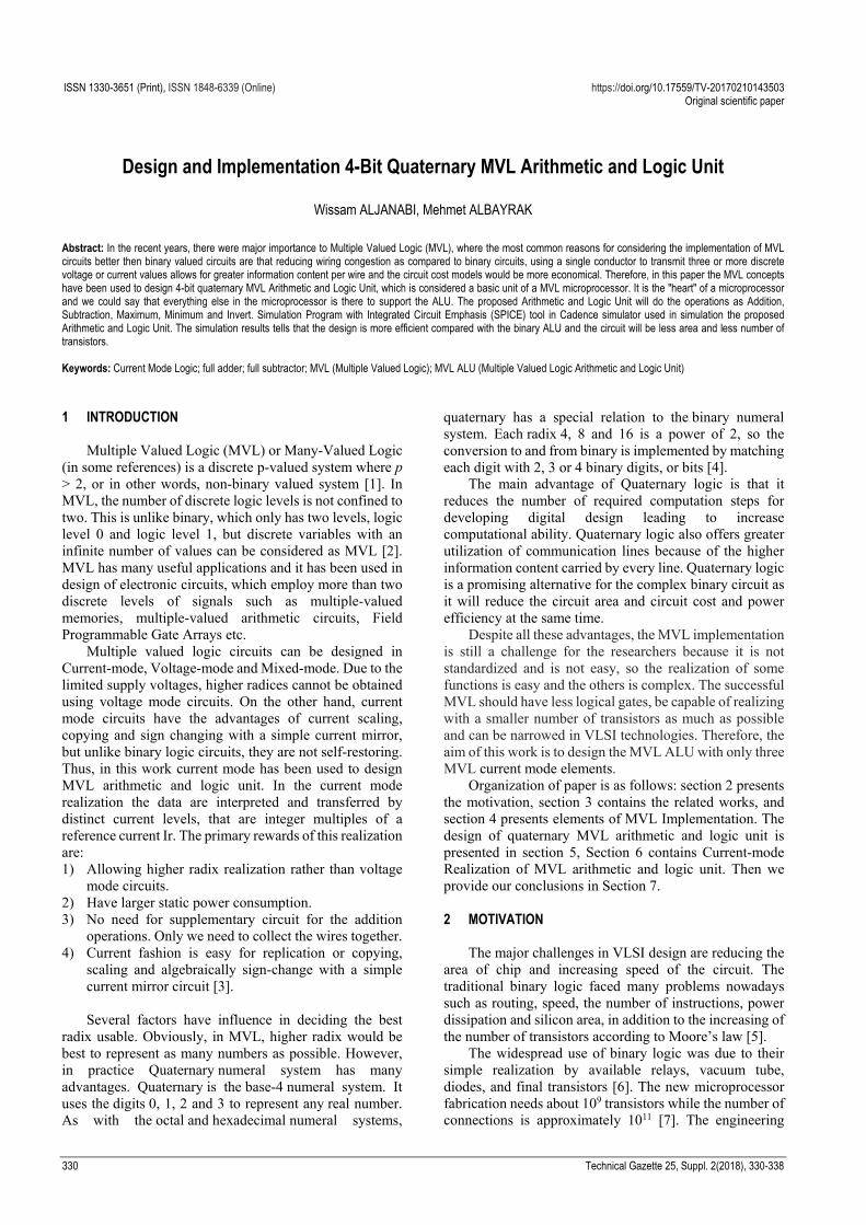
2) Current mirror: Circuits that producing the multiple of current are called mirrors circuits. The simple current mirror shown in Fig. 1. This operation attribute is very important in the current-mode implementation.
Figure 1 Current mirror
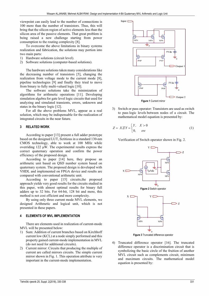
3) Switch or pass operator: Transistors are used as switch
to pass logic levels between nodes of a circuit. The mathematical model equation is presented by:
0
0Y , X
Z X Y, ow
Ξ>
= =
(1)
Verification of Switch operator shown in Fig. 2.
Figure 2 Switch operator
Figure 3 Truncated difference operator
4) Truncated difference operator [16]. The truncated
difference operator is a discrimination circuit that is symbolizing the basic circle of the fruition of another MVL circuit such as complements circuit, minimum and maximum circuits. The mathematical model equation is presented by:

Wissam ALJANABI, Mehmet ALBAYRAK: Design and Implementation 4-Bit Quaternary MVL Arithmetic and Logic Unit
332 Technical Gazette 25, Suppl. 2(2018), 330-338
X Y0
X Y , X YZ
, owΞ
− ≥= =
(2)
Verification of truncated difference circuit requires an n-type CMOS current mirror circuit.
5 DESIGN OF QUATERNARY MVL ARITHMETIC AND
LOGIC UNIT The proposed ALU is one of the most important
components in a MVL microprocessor, and is typically the part of the processor that is designed first. Once the MVLALU is designed, the rest of the MVL microprocessor is implemented to feed operands and control codes to the MVL ALU. This unit typically need to be able to perform operations as an Addition, Subtraction, Maximum, Minimum and Invert. A basic MVL ALU design involves a collection of "MVL ALU Slices", which each can perform the specified operation. The block diagram of 1-bit MVL ALU shown in Fig. 4.
Figure 4 Block diagram of 1 bit MVL ALU
Figure 5 Block diagram of 4-bit MVL ALU
To extend the MVL ALU from 1 bit to 4-bit not require
more than connect 4 circuits in cascade. Thus, the block diagram of 4-bit MVL ALU shown in Fig. 5.
6 CURRENT-MODE REALIZATION OF MVL ARITHMETIC AND LOGIC UNIT
In this work, for realizing the "MVL ALU Slices",
current-mode realization has been used and the reference current level Ir, is chosen as 5 μA and increases with its integer multiples as indicated in Tab. 1.
Table 1 Current levels and logic levels equivalent
Logic level Current Level (μA) 0 0 1 5 2 10 3 15
The specified current levels can vary from their
original values due to some differences in active element dimension, power supplies, technology parameters, etc. This difference can be tolerated and output can be sensed correctly for a range of value that is called noise margin. Considering the presence of current deviances from their original values, logic levels be specified as follows,
0, 2.5 μA1, 2.5 μA 7.5 μA2, 7.5 μA 12.5 μA3, 12.5 μA 15 μA
II
II
I
< ≤ <= ≤ < ≤ <
(3)
Computer Aided Design (CAD) for simulating the
integrated circuits is also another issue facing the development and design of IC’s, so that the choice of best simulation software package is another challenge. Packages existed a many simulation software for realizing an RTL circuits like, FPGA, Microprocessor, etc. The famous CAD packages now days are MATLAB, CADENCE, HSPICE, PSIM and others. In this work will use cadence package for achieving design and implementation targets. Simulation Program with Integrated Circuit Emphasis (SPICE) tool in Cadence simulator used in simulation the proposed MVL ALU.
6.1 Implementation of Quaternary Full Adder
One of the most important "MVL ALU Slices" is the
full adder circuit, which represent a core of MVL ALU; therefore, the design and implementation of such circuit is very significant. The proposed design of full adder circuit depends mainly on the truncated difference operator, switch or pass operator and Current mirror, all of which has been mentioned before. The mathematical model for full adder is presented by:
{ , 3( , , )
( ) (4),A B Cin A B Cin
Sum A B CinA B Cin ow
+ + + + ≤=
+ + − (4)
{0, 31,
A B CinCout
ow+ + ≤
= (5)
For verification the first conditional part of Eq. (4), (if
A + B + Cin ≤ 3, Sum(A, B, Cin) = A + B + Cin), the design requires two truncated difference operator and one switch

Wissam ALJANABI, Mehmet ALBAYRAK: Design and Implementation 4-Bit Quaternary MVL Arithmetic and Logic Unit
Tehnički vjesnik 25, Suppl. 2(2018), 330-338 333
operator. In addition, there is no need for supplementary circuit for the addition of (A + B + Cin). Only we need collect the wires together based on Kirchhoff current low (KCL). Fig. 6 illustrated the transistor schematic diagram for this part.
Figure 6 Transistor schematic diagram for first conditional part of Eq. (4)
For verification the second conditional part of Eq. (4),
(if A + B + Cin > 3, Sum(A, B, Cin) = (A + B + Cin) – (4)),it is clear this design not requires more than one truncated difference operator. Fig. 7 illustrated the transistor schematic diagram for this part.
Figure 7 Transistor diagram for second conditional part of Eq. (4)
In order to implement the Eq. (4) entirely, that does not
require more than collect the two design above together. For verification the Eq. (5) entirely, this design
requires one truncated difference operator and one switch operator. Fig. 8 illustrated the transistor schematic diagram for this function.
Figure 8 Transistor schematic diagram for Eq. (5).
Fig. 9 give the transistor level design for the 1-bit
quaternary full adder circuit. This design requires 12 transistors. It was also noted in this design requires a value of (A + B + Cin) in three different nodes to solve the problem we can use internal current mirror, which produces identical copies for current value of (A + B + Cin).
Figure 9 The transistor level design for the 1-bit quaternary full adder circuit
6.2 Implementation of Quaternary Full Subtractor
The quaternary full subtractor is an electronic
circuit which is used to perform subtraction of three input quaternary bits: the minuend (A), subtrahend (B) and borrow in (Bin). The full subtractor generates two output bits: the difference (D) and borrow out (Bout) is set when the previous digit borrowed from (A). Thus, (Bin) is also subtracted from (A) as well as the subtrahend (B). On the other hand, in symbols: D = A – B − Bin.
In mathematic sand computing, the method of complements is a technique used to subtract one number from another using only addition of positive numbers. This method was commonly used in mechanical calculators and is still used in modern computers.
In binary system, when we want to subtract 4-bit binary number from another 4-bit binary number by using complements method, first: we must get the one's complement for subtrahend number, where the one's complement of a binary digit is the number that must be added to it to produce 1, second: we must add 1to the first bit of the one's complement number in order to convert the negative number to its positive representation and third: making ordinary addition operation and the output will be the result of subtraction.
In quaternary system, we can repeat the same steps with some modification. Therefore, when we want to subtract 4-bit quaternary number from another 4-bit quaternary number by using complements method, first: we must get the three's complement for subtrahend number, where the three's complement of a quaternary digit is the number that must be added to it to produce 3, thus the three's complement for (0=3), (1=2), (2=1) and (3=0), second: we must add 1to the first bit of the three's complement number in order to convert the negative number to its positive representation and third: making ordinary addition operation and the output will be the result of subtraction. For example:

Wissam ALJANABI, Mehmet ALBAYRAK: Design and Implementation 4-Bit Quaternary MVL Arithmetic and Logic Unit
334 Technical Gazette 25, Suppl. 2(2018), 330-338
• The subtrahend number is 1302. • The three's complement of 1302 is 2031 (because
three's complement of 0=3, three's complement of 1=2, three's complement of 2=1 and three's complement of 3=0).
• Adding 1 to the first bit of 2031 will be 2032
• This number (2032) represents the positive form of this negative number (−1302).
• Adding (2032) to (3012)
According to the above information the proposed quaternary full subtractor is implemented within the quaternary full adder but the first bit of subtrahend number must enter into three's complement circuit and adding 1 for the result before entering to full adder circuit and the others bits of subtrahend number must enter into three's complement circuit before entering to full adder circuit. Fig. 10 shows the block diagram of the proposed 4-bit quaternary full subtractor circuit. The mathematical model for three's complement is presented by:
0, 31, 2
( )2, 13, 0
BB
Three's complement BBB
= == = =
(6)
Figure 10 The block diagram of the proposed 4-bit quaternary full subtractor
circuit In transistor level realization of three's complement
circuit, we noted, there is possible to get the three's complement for quaternary number by subtract it from 3.
Therefore, we adjusted the Eq. (6) to be simpler and presented by:
( ) 3Three's complement B B= − (7)
For verification the Eq. (7), it is clear this design requires only one truncated difference operator. Fig. 11 illustrated the transistor schematic diagram for this function.
Figure 11 The transistor schematic diagram for Eq. (7)
From the disadvantages of truncated difference
operator, when the two inputs for this operator be large and equal, for example 15 µA, the output will not be 0. Therefore, to improve the performance of this circuit, one switch operator and two truncated difference operator have been added to the design. Fig. 12 illustrated the transistor schematic diagram of final three's complement circuit.
Figure 12 Transistor schematic diagram of final three's complement circuit One of the challenges that we faced in the design of the
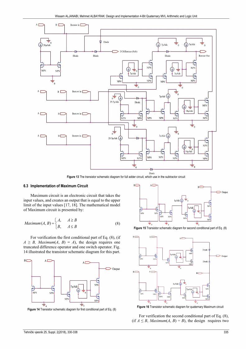
proposed full subtractor circuit is that, when the subtrahend (B = 0), the three's complement of B is 3 and by adding 1 to this number to convert it to the positive representation, the second input value of full adder circuit will be 4 with assuming that A = 3 and borrow in = 1. Therefore, in this case: D = 3 + 4 + 1 = 8. The quaternary representation of 8 is 0 with borrow out = 2. Consequently, to solve this problem the design of full adder circuit, which use in the subtractor circuit, require some modification in order to be able to generate in this case two output bits: the difference (D = 0) and borrow out (Bout =2). Fig. 13 illustrated the transistor schematic diagram for full adder circuit after the modification.
Wissam ALJANABI, Mehmet ALBAYRAK: Design and Implementation 4-Bit Quaternary MVL Arithmetic and Logic Unit
Tehnički vjesnik 25, Suppl. 2(2018), 330-338 335
Figure 13 The transistor schematic diagram for full adder circuit, which use in the subtractor circuit
6.3 Implementation of Maximum Circuit
Maximum circuit is an electronic circuit that takes the
input values, and creates an output that is equal to the upper limit of the input values [17, 18]. The mathematical model of Maximum circuit is presented by:
,
( , ),
A A BMaximum A B
B A B≥
= ≤ (8)
For verification the first conditional part of Eq. (8), (if
A ≥ B, Maximum(A, B) = A), the design requires one truncated difference operator and one switch operator. Fig. 14 illustrated the transistor schematic diagram for this part.
Figure 14 Transistor schematic diagram for first conditional part of Eq. (8)
Figure 15 Transistor schematic diagram for second conditional part of Eq. (8)
Figure 16 Transistor schematic diagram for quaternary Maximum circuit
For verification the second conditional part of Eq. (8),
(if A ≤ B, Maximum(A, B) = B), the design requires two

Wissam ALJANABI, Mehmet ALBAYRAK: Design and Implementation 4-Bit Quaternary MVL Arithmetic and Logic Unit
336 Technical Gazette 25, Suppl. 2(2018), 330-338
truncated difference operator and one switch operator. Fig. 15 illustrated the transistor schematic diagram for this part.
Fig. 16 give the transistor level design for quaternary Maximum circuit. This design requires 12 transistors. 6.4 Implementation of Minimum Circuit
Minimum circuit is an electronic circuit that takes the
input values, and creates an output that is equal to the lower limit of the input values. The mathematical model of Maximum circuit is presented by:
,
( , ),
A A BMinimum A B
B A B≤
= ≥ (9)
The transistor level design for quaternary Minimum
circuit somewhat similar to the transistor level design for quaternary Maximum circuit because of the similarities in mathematical models of these circuits (except ≥ in the first model has reversed in the second model). Therefore, the transistor level design for quaternary Minimum circuit is the design for quaternary Maximum circuit with a reverse of switch operators inputs from A to B and vice versa.
Figure 17 Transistor schematic diagram of quaternary Minimum circuit
6.5 Implementation of Quaternary Inverter Circuit
In digital logic, an inverter or NOT is a logic circuit
which implements logical negation. The mathematical model for quaternary inverter is presented by:
0, 31, 2
( )2, 13, 0
BB
Inverter BBB
= == = =
(10)
It is very clear the similarity between the mathematical
model for quaternary inverter and the mathematical model for three's complement. Therefore, the transistor level design for quaternary Inverter circuit similar to the transistor level design for quaternary three's complement circuit, that has been previously explained in detail.
6.6 Implementation of Selector Circuit The MVL selector or (multiplexer) is classified as a
combinational circuit that choose one of the run input lines based on a set of selection lines and leads it to a single output wire [3]. In the proposed selector, there are 6 run input lines and 6 selection lines whose value groupings control which input to pass. The design of the proposed selector is shown in Fig. 18 and the operators is given in Tab. 2.
Figure 18 The design of the proposed MVL selector
Table 2 The operators of MVL selector
S OUT 0 µA I0 5 µA I1 10 µA I2 15 µA I3 20 µA I4 25 µA I5
There is no need for maximum circuit when the
realization of selector circuit using current mode. This gain because of zero cost addition process in current mode realization.
Before the realization of selector gates (Gate1, Gate2, Gate3, Gate4, Gate5 and Gate6), we must put the mathematical models for these gates. The mathematical models for selector gates are presented by:
0
0, 0
Gate1( , )0,I S
I Sow=
=
(11)
11
, 5 μAGate2( , )
0,I S
I Sow=
=
(12)
22
, 10 μAGate3( , )
0,I S
I Sow
==
(13)
33
, 15 μAGate4( , )
0,I S
I Sow
==
(14)

Wissam ALJANABI, Mehmet ALBAYRAK: Design and Implementation 4-Bit Quaternary MVL Arithmetic and Logic Unit
Tehnički vjesnik 25, Suppl. 2(2018), 330-338 337
44
, 20 μAGate5( , )
0,I S
I Sow
==
(15)
55
, 25 μAGate6( , )
0,I S
I Sow
==
(16)
In the transistor level design for these gates, for
verification the Eq. (11) entirely; the design requires one truncated difference operator and one switch operator. Fig. 19 illustrated the transistor schematic diagram for this function.
Figure 19The transistor schematic diagram for Eq. (11)
Figure 20 The transistor schematic diagram for other functions
For verification the other functions, the design of these
gates is similar but the parameters which have been indicated inside the boxes in Fig. 20 below, must change according to each function so as to be in the higher box smaller than the conditional value of S in this function by 2 µA and in the lower box Larger than S value by 2 µA. The design requires three truncated difference operator and one switch operator. Fig. 20 illustrated the transistor schematic diagram for these functions.
Fig. 21 represents cadence simulation results for MVL ALU circuit.
Figure 21 Cadence simulation results for the proposed MVL ALU circuit
7 CONCLUSION
Proposed 4-bit Quaternary MVL ALU is designed and
implemented using 848 n-type transistors, 392 p-type transistors and 112 diodes. However, the 4-bit binary Intel 4004 ALU was subsequently designed using silicon gate

Wissam ALJANABI, Mehmet ALBAYRAK: Design and Implementation 4-Bit Quaternary MVL Arithmetic and Logic Unit
338 Technical Gazette 25, Suppl. 2(2018), 330-338
technology and built of approximately 2300 transistors [21] as the 4-bit Quaternary MVL ALU is equivalent in efficiency and performance to 8 bit binary ALU because the largest number in 4-bit quaternary system is 3333, which is equivalent in the decimal system 255 and the largest number in 8 bit binary system is 11111111, which is equivalent to decimal system 255.
From the analysis of Fig. 21 the propagation delay (gate delay) was nearly 0.25 μs. Consequently, the Proposed MVL ALU is designed with small size, more efficient and low cost. All simulations have been performed in cadence package simulator.
There are many opportunities for extending the scope of this work particularly what relevant in designing and implementing of MVL microprocessor based on Current mode elements, design a high radix ALU and microprocessors for reducing the size and power consumptions and redesign a new microprocessor instructions to be more suitable for MVL in general. The future may need MVL clock as all current works in the sequential MVL circuits are using binary clock that open a new research field. We think the improvement of the ALU design can be really a promising field for future researchers and extensive research in this sector will enhance the performance of processor, as ALU is the heart of computer system.
8 REFERENCES [1] Elena, D. (1999). Multiple-Valued Logic in VLSI:
Challenges and Opportunities. Proceedings of NORCHIP'99 / Oslo, Norway, November 8-9, 340-350.
[2] Michael, M. & Mitchell, A. T. (2008). Multiple Valued Logic: Concepts and Representations. A Publication in the Morgan & Claypool Publishers series. https://doi.org/10.2200/S00065ED1V01Y200709DCS012
[3] Hisham, L. S. & Dhafer, R. Z. (2014). Design and Implementation of a Multiple-Valued Logic FPGA Based on Convert-Coded-Collect (CCCi) Space Theory. International Journal of Computer Science Engineering and Information Technology Research (IJCSEITR), 4(4), 95-102.
[4] Leela, B. R. & Narayana, R. (2005). VLSI Implementation of Fast Addition Subtraction and Multiplication (Unsigned) Using Quaternary Signed Digit Number System. International Journal & Magazine of Engineering Technology Management and Research, 2(12), 2060-2073.
[5] Haissam, E. (2014). Structural and Hardware Complexities of Microprocessor Design According to Moore’s Law. International Journal of Computer Science and Information Technology, 6(4), 175-183. https://doi.org/10.5121/ijcsit.2014.6411
[6] Zvonko, G. V. & Kenneth, C. S. (1974). Engineering Aspects of Multi-Valued Logic Systems. IEEE Transection on Computer, 7(9), 34-41. https://doi.org/10.1109/MC.1974.6323306
[7] Haissam, E. (2015). Increasing the Transistor Count by Constructing a Two-Layer Crystal Square on a Single Chip. International Journal of Computer Science & Information Technology (IJCSIT), 7(3), 97-105. https://doi.org/10.5121/ijcsit.2015.7308
[8] Kenneth, C. S. (1988). Multiple-Valued Logic: A Tutorial and Appreciation. IEEE Transection on Computer, Survey & Tutorial Series, 4, 17-27.
[9] Michell, J. A. (2013). Design and Architecture for Digital Signal Processing. Ed. Ruiz, G. Published by InTech. https://doi.org/10.5772/3456
[10] Muzio, J. C. & Rosenerg, I. C. (1986). Introduction-Multiple-Valued Logic. IEEE Transections on Computers, 35(2), 97-98. https://doi.org/10.1109/TC.1986.1676726
[11] Luccio, F. & Pinotti, M. C. (1991). Minimal Synthesis of Multivalued Functions with New Operators. Computers and Digital Techniques IEEE Proceedings, 138(6), 419-423.
[12] Hayes, J. P. (1986). Digital Simulation with Multiple Logic Values. IEEE Transections on Computer-Aided Design, 5(2), 274-283. https://doi.org/10.1109/TCAD.1986.1270196
[13] Brito, D., Rabuske, T. G., Fernandes, J. R., Flores, P., & Monteiro, J. (2015). Quaternary Logic Look up Table in Standard CMOS. IEEE Transaction on Very Large Scale Integration System, 23(2), 306-316. https://doi.org/10.1109/TVLSI.2014.2308302
[14] Nagamani, A. N. & Nischai, S. (2011). Quaternary High Performance Arithmetic Logic Unit Design. 14th Euromica Conference / Oulu, Finland, 148-153. https://doi.org/10.1109/DSD.2011.23
[15] Marcus, R., Carlos, A. L., Luigi, C., Cristiano, L. (2010). A cost effective Technique for Mapping BLUTs to QLUTs in FPGAs. International Conference on Field Programmable Logic and Applications / Milano, Italy, 332-335. https://doi.org/10.1109/FPL.2010.72
[16] Turgay, T. & Avni, M. (2004). Implementation of Multi-Valued Logic Gates Using Full Current-Mode CMOS Circuits. Analog Integrated Circuits and Signal Processing, 39, 191-204. https://doi.org/10.1023/B:ALOG.0000024066.66847.89
[17] Fatima, S. & Avni, M. (2013). AB Flip-Flop, a First Step to Multilevel Sequential Logic. Journal of Analog Integrated Circuits and Signal Processing, 74(1), 91-96.
[18] Turgay, T. & Avni, M. (2002). Multi-Valued Logic Function Implementation with Novel Current-Mode Logic Gates. IEEE International Symposium on Circuits and Systems / Phoenix-Scottsdale, AZ, USA, 881-884.
[19] Current, K. (1995). Memory Circuits for Multiple Valued Logic Voltage Signals. Proceedings of the 25th International Symposium on Multiple Valued Logic / Bloomington, IN, USA, 52-57. https://doi.org/10.1109/ISMVL.1995.513509.
[20] Gauri, P. & Seema, S. W. (2015). Design of CMOS Galois Field Arithmetic Logic Unit Using 120nm BSIM-4 model. International Research Journal of Engineering and Technology (IRJET), 2(3), 1372-1376.
[21] Federico, F. (2015). The MOS Silicon Gate Technology and the First Microprocessors. La Rivista del Nuovo Cimento, 38(12), 575-621. https://doi.org/10.1393/ncr/i2015-10119-7
Contact information: Wissam ALJANABI, M.Sc, PhD student Department of Electronics and Communication Engineering, Suleyman Demirel University, Cunur, 32260 Isparta, Turkey [email protected] Mehmet ALBAYRAK, Asst. Prof. Dr. Department of Computer Tech., Distance Learning Voc. Sch. Suleyman Demirel University Cunur, 32260 Isparta, Turkey [email protected]