Design and Fabrication - University of California, San...
28
© 2002 by CRC Press LLC II Design and Fabrication 15 Materials for Microelectromechanical Systems Christian A. Zorman, Mehran Mehregany Introduction • Single-Crystal Silicon • Polysilicon • Silicon Dioxide • Silicon Nitride • Germanium-Based Materials • Metals • Silicon Carbide • Diamond • III–V Materials • Piezoelectric Materials • Conclusions 16 MEMS Fabrication Marc J. Madou Micromachining: Introduction • Historical Note • Silicon Crystallography • Silicon as a Substrate and Structural Material • Wet Isotropic and Anisotropic Etching • Etching With Bias and/or Illumination of the Semiconductor • Etch-Stop Techniques • Problems with Wet Bulk Micromachining • Wet Bulk Micromachining Examples • Surface Micromachining: Introduction • Historical Note • Mechanical Properties of Thin Films • Surface Micromachining Processes • Poly-Si Surface Micromachining Modifications • Non-Poly-Si Surface Micromachining Modifications • Resists as Structural Elements and Molds in Surface Micromachining • Materials Case Studies • Polysilicon Surface Micromachining Examples 17 LIGA and Other Replication Techniques Marc J. Madou Introduction • LIGA Processes—Introduction to the Technology • LIGA Applications • Technological Barriers and Competing Technologies 18 X-Ray-Based Fabrication Todd Christenson Introduction • DXRL Fundamentals • Mold Filling • Material Characterization and Modification • Planarization • Angled and Re-entrant Geometry • Multilayer DXRL Processing • Sacrificial Layers and Assembly • Applications • Conclusions 19 Electrochemical Fabrication (EFAB™) Adam L. Cohen Introduction • Background • A New SFF Process • Instant Masking • EFAB • Detailed Process Flow • Microfabricated Structures • Automated EFAB Process Tool • Materials for EFAB • EFAP Performance • EFAB Compared with Other SFF Processes • EFAB Compared with Other Microfabrication Processes • EFAB Limitations and Shortcomings • EFAB Applications • The Future of EFAB 20 Fabrication and Characterization of Single-Crystal Silicon Carbide MEMS Robert S. Okojie Introduction • Photoelectrochemical Fabrication Principles of 6H-SiC • Characterization of 6H-SiC Gauge Factor • High-Temperature Metallization • Sensor Characteristics • Summary
Transcript of Design and Fabrication - University of California, San...

IIDesign and Fabrication
15 Materials for Microelectromechanical Systems Christian A. Zorman, Mehran MehreganyIntroduction • Single-Crystal Silicon • Polysilicon • Silicon Dioxide • Silicon Nitride• Germanium-Based Materials • Metals • Silicon Carbide • Diamond • III–V Materials• Piezoelectric Materials • Conclusions
16 MEMS Fabrication Marc J. MadouMicromachining: Introduction • Historical Note • Silicon Crystallography • Silicon as aSubstrate and Structural Material • Wet Isotropic and Anisotropic Etching • Etching WithBias and/or Illumination of the Semiconductor • Etch-Stop Techniques • Problems withWet Bulk Micromachining • Wet Bulk Micromachining Examples • SurfaceMicromachining: Introduction • Historical Note • Mechanical Properties of ThinFilms • Surface Micromachining Processes • Poly-Si Surface MicromachiningModifications • Non-Poly-Si Surface Micromachining Modifications • Resists as StructuralElements and Molds in Surface Micromachining • Materials Case Studies • PolysiliconSurface Micromachining Examples
17 LIGA and Other Replication Techniques Marc J. MadouIntroduction • LIGA Processes—Introduction to the Technology • LIGA Applications• Technological Barriers and Competing Technologies
18 X-Ray-Based Fabrication Todd ChristensonIntroduction • DXRL Fundamentals • Mold Filling • Material Characterization andModification • Planarization • Angled and Re-entrant Geometry • Multilayer DXRLProcessing • Sacrificial Layers and Assembly • Applications • Conclusions
19 Electrochemical Fabrication (EFAB™) Adam L. CohenIntroduction • Background • A New SFF Process • Instant Masking • EFAB• Detailed Process Flow • Microfabricated Structures • Automated EFAB Process Tool• Materials for EFAB • EFAP Performance • EFAB Compared with Other SFFProcesses • EFAB Compared with Other Microfabrication Processes • EFAB Limitations and Shortcomings • EFAB Applications • The Future of EFAB
20 Fabrication and Characterization of Single-Crystal Silicon Carbide MEMS Robert S. OkojieIntroduction • Photoelectrochemical Fabrication Principles of 6H-SiC • Characterizationof 6H-SiC Gauge Factor • High-Temperature Metallization • Sensor Characteristics• Summary
© 2002 by CRC Press LLC
21 Deep Reactive Ion Etching for Bulk Micromachining of Silicon Carbide Glenn M. BeheimIntroduction • Fundamentals of High-Density Plasma Etching • Fundamentals of SiCEtching Using Fluorine Plasmas • Applications of SiC DRIE: Review • Applications of SiCDRIE: Experimental Results • Applications of SiC DRIE: Fabrication of a BulkMicromachined SiC Pressure Sensor • Summary
22 Microfabricated Chemical Sensors for Aerospace Applications Gary W. Hunter, Chung-Chiun Liu, Darby B. MakelIntroduction • Aerospace Applications • Sensor Fabrication Technologies• Chemical Sensor Development • Future Directions, Sensor Arrays andCommercialization • Commercial Applications • Summary
23 Packaging of Harsh-Environment MEMS Devices Liang-Yu Chen, Jih-Fen LeiIntroduction • Material Requirements for Packaging Harsh-Environment MEMS• High-Temperature Electrical Interconnection System • Thermomechanical Propertiesof Die-Attach • Discussion
© 2002 by CRC Press LLC
15Materials for
MicroelectromechanicalSystems
15.1 Introduction15.2 Single-Crystal Silicon15.3 Polysilicon15.4 Silicon Dioxide15.5 Silicon Nitride15.6 Germanium-Based Materials15.7 Metals15.8 Silicon Carbide15.9 Diamond15.10 III–V Materials15.11 Piezoelectric Materials15.12 Conclusions
15.1 Introduction
Without question, one of the most exciting technological developments during the last decade of the20th century was the field of microelectromechanical systems (MEMS). MEMS consists of microfabri-cated mechanical and electrical structures working in concert for perception and control of the localenvironment. It was no accident that the development of MEMS accelerated rapidly during the 1990s,as the field was able to take advantage of innovations created during the integrated circuit revolution ofthe 1960s to the 1980s, in terms of processes, equipment and materials. A well-rounded understandingof MEMS requires a mature knowledge of the materials used to construct the devices, as the materialproperties of each component can influence device performance. Because the fabrication of MEMSstructures often depends on the use of structural, sacrificial and masking materials on a commonsubstrate, issues related to etch selectivity, adhesion, microstructure and a host of other properties areimportant design considerations. A discussion of the materials used in MEMS is really a discussion ofthe material systems used in MEMS, as the fabrication technologies rarely utilize a single material, butrather a collection of materials, each providing a critical function. It is in this light that this chapter isconstructed. This chapter does not attempt to present a comprehensive review of all materials used inMEMS because the list of materials is just too long. It does, however, detail a selection of material systemsthat illustrate the importance of viewing MEMS in terms of material systems as opposed to individualmaterials.
Christian A. ZormanCase Western Reserve University
Mehran MehreganyCase Western Reserve University
© 2002 by CRC Press LLC

15.2 Single-Crystal Silicon
Use of silicon (Si) as a material for microfabricated sensors can be traced to 1954, when the first paperdescribing the piezoresistive effect in germanium (Ge) and Si was published [Smith, 1954]. The resultsof this study suggested that strain gauges made from these materials could be 10 to 20 times larger thanthose for conventional metal strain gauges, which eventually led to the commercial development of Sistrain gauges in the late 1950s. Throughout the 1960s and early 1970s, techniques to mechanically andchemically micromachine Si substrates into miniature, flexible mechanical structures on which the straingauges could be fabricated were developed and ultimately led to commercially viable, high-volumeproduction of Si-based pressure sensors in the mid 1970s. These lesser known developments in Simicrofabrication technology happened concurrently with more popular developments in the areas of Si-based solid-state devices and integrated-circuit (IC) technologies that have revolutionized modern life.The conjoining of Si IC processing with Si micromachining techniques during the 1980s marked theadvent of MEMS, and positioned Si as the primary material for MEMS.
There is little question that Si is the most widely known semiconducting material in use today. Single-crystal Si has a diamond (cubic) crystal structure. It has an electronic band gap of 1.1 eV, and, like manysemiconducting materials, it can be doped with impurities to alter its conductivity. Phosphorus (P) is acommon dopant for n-type Si and boron (B) is commonly used to produce p-type Si. A solid-phase oxide(SiO2) that is chemically stable under most conditions can readily be grown on Si surfaces. Mechanically, Siis a brittle material with a Young’s modulus of about 190 GPa, a value that is comparable to steel (210 GPa).Si is among the most abundant elements on Earth that can readily be refined from sand to produceelectronic-grade material. Mature industrial processes exist for the low-cost production of single-crystalSi wafered substrates that have large surface areas (>8-in. diameter) and very low defect densities.
For MEMS applications, single-crystal Si serves several key functions. Single-crystal Si is perhaps themost versatile material for bulk micromachining, owing to the availability of well-characterized aniso-tropic etches and etch-mask materials. For surface micromachining applications, single-crystal Si sub-strates are used as mechanical platforms on which device structures are fabricated, whether they are madefrom Si or other materials. In the case of Si-based integrated MEMS devices, single-crystal Si is theprimary electronic material from which the IC devices are fabricated.
Bulk micromachining of Si uses wet and dry etching techniques in conjunction with etch masks and etchstops to sculpt micromechanical devices from the Si substrate. From the materials perspective, two keycapabilities make bulk micromachining a viable technology: (1) the availability of anisotropic etchants suchas ethylene-diamine pyrocatecol (EDP) and potassium hydroxide (KOH), which preferentially etch single-crystal Si along select crystal planes; and (2) the availability of Si-compatible etch-mask and etch-stopmaterials that can be used in conjunction with the etch chemistries to protect select regions of the substratefrom removal.
One of the most important characteristics of etching is the directionality (or profile) of the etching process.If the etch rate in all directions is equal, the process is said to be isotropic. By comparison, etch processes thatare anisotropic generally have etch rates in the direction perpendicular to the wafer surface that are muchlarger than the lateral etch rates. It should be noted that an “anisotropic” sidewall profile could also beproduced in virtually any Si substrate by deep reactive ion etching, ion beam milling or laser drilling.
Isotropic etching of a semiconductor in liquid reagents is commonly used for removal of work-damaged surfaces, creation of structures in single-crystal slices, and patterning single-crystal or polycrys-talline semiconductor films. For isotropic etching of Si, the most commonly used etchants are mixturesof hydrofluoric (HF) and nitric (HNO3) acid in water or acetic acid (CH3COOH), usually called theHNA etching system.
Anisotropic Si etchants attack the (100) and (110) crystal planes significantly faster than the (111)crystal planes. For example, the (100) to (111) etch-rate ratio is about 400:1 for a typical KOH/wateretch solution. Silicon dioxide (SiO2), silicon nitride (Si3N4) and some metallic thin films (e.g., Cr, Au)provide good etch masks for most Si anisotropic etchants. In structures requiring long etching times inKOH, Si3N4 is the preferred masking material, due to its chemical durability.
© 2002 by CRC Press LLC

In terms of etch stops, heavily B-doped Si (>7 × l019
/cm3), commonly referred to as a p+ etch stop, is
effective for some etch chemistries. Fundamentally, etching is a charge transfer process, with etch ratesdependent on dopant type and concentration. Highly doped material might be expected to exhibit higheretch rates because of the greater availability of mobile carriers. This is true for isotropic etchants such asHNA, where typical etch rates are 1 to 3 µm/min for p- or n-type dopant concentrations greater than10
18/cm
3 and essentially zero for concentrations less than 10
17/cm
3. On the other hand, anisotropic
etchants such as EDP and KOH exhibit a much different preferential etching behavior. Si that is heavilydoped with B (>7 × 10
19/cm3) etches at a rate that is about 5 to 100 times slower than undoped Si when
etched in KOH and 250 times slower when etched in EDP. Etch stops formed by the p+ technique areoften less than 10 µm thick, as the B doping is often done by diffusion. Using high diffusion temperatures(e.g., 1175°C) and long diffusion times (e.g., 15 to 20 hours), thick (∼20 µm) p+ etch stop layers can becreated. It is also possible to create a p+ etch stop below the Si surface using ion implantation; however,the implant depth is limited to a few microns and a high-energy/high-current ion accelerator is requiredfor implantation. While techniques are available to grow a B-doped Si epitaxial layer on top of a p+ etchstop to increase the thickness of the final structure, this is seldom utilized due to the expense of theepitaxial process step.
Due to the high concentration of B, p+ Si has a high density of defects. These defects are generatedas a result of stresses created in the Si lattice due to the fact that B is a smaller atom than Si. Studies ofp+ Si report that stress in the resultant films can either be tensile [Ding et al., 1990] or compressive[Maseeh and Senturia, 1990]. These variations may be due to post-processing steps. For instance, thermaloxidation can significantly modify the residual stress distribution in the near-surface region of p+ Sifilms, thereby changing the overall stress in the film. In addition to the generation of crystalline defects,the high concentration of dopants in the p+ etch-stops prevents the fabrication of electronic devices inthese layers. Despite some of these shortcomings, the p+ etch-stop technique is widely used in Si bulkmicromachining due to its effectiveness and simplicity.
A large number of dry etch processes are available to pattern single-crystal Si. The process spectrumranges from physical etching via sputtering and ion milling to chemical plasma etching. Two processes,reactive ion etching (RIE) and reactive ion beam etching (RIBE) combine aspects of both physical andchemical etching. In general, dry etch processes utilize a plasma of ionized gases, along with neutralparticles to remove material from the etch surface. Details regarding the physical processes involved indry etching can be found elsewhere [Wolfe and Tauber, 1999].
Reactive ion etching is the most commonly used dry etch process to pattern Si. In general, fluorinatedcompounds such as CF4, SF6 and NF3 or chlorinated compounds such as CCl4 or Cl2 sometimes mixedwith He, O2 or H2 are used. The RIE process is highly directional, thereby enabling direct pattern transferfrom the masking material to the etched Si surface. The selection of masking material is dependent onthe etch chemistry and the desired etch depth. For MEMS applications, photoresist and SiO2 thin filmsare often used. Si etch rates in RIE processes are typically less than 1 µm/min, so dry etching is mostlyused to pattern layers on the order of several microns in thickness. The plasmas selectively etch Si relativeto Si3N4 or SiO2, so these materials can be used as etch masks or etch-stop layers. Recent developmentof deep reactive ion etching processes has extended Si etch depths well beyond several hundred microns,thereby enabling a multitude of new designs for bulk micromachined structures.
15.3 Polysilicon
Without doubt the most common material system for the fabrication of surface micromachined MEMSdevices utilizes polycrystalline Si (polysilicon) as the primary structural material, SiO2 as the sacrificialmaterial and Si3N4 for electrical isolation of device structures. Heavy reliance on this material systemstems in part from the fact these three materials find uses in the fabrication of ICs and, as a result, filmdeposition and etching technologies are readily and widely available. Like single-crystal Si, polysiliconcan be doped during or after film deposition using standard IC processing techniques. SiO2 can be grownor deposited over a broad temperature range (e.g., 200 to 1150°C) to meet various process and material
© 2002 by CRC Press LLC
requirements. SiO2 is readily dissolvable in hydrofluoric acid (HF), an IC-compatible chemical, withoutetching the polysilicon structural material [Adams, 1988]. HF does not wet bare Si surfaces; as a result,it is automatically rejected from microscopic cavities in between polysilicon layers after a SiO2 sacrificiallayer is completely dissolved.
For surface micromachined structures, polysilicon is an attractive material because it has mechanicalproperties that are comparable to single-crystal Si, the required processing technology has been developedfor IC applications, and it is resistant to SiO2 etchants. In other words, polysilicon surface microma-chining leverages on the significant capital investment made by the IC industry in the important areasof film deposition, patterning and material characterization.
For MEMS and IC applications, polysilicon thin films are commonly deposited by a process knownas low-pressure chemical vapor deposition (LPCVD). This deposition technique was first commercializedin the mid-1970s [Rosler, 1977] and has since been a standard process in the microelectronics industry.The typical polysilicon LPCVD reactor (or furnace) is based on a hot-wall, resistance-heated, horizontal,fused-silica tube design. The temperature of the wafers in the furnace is maintained by heating the tubeusing resistive heating elements. The furnaces are equipped with quartz boats that have closely spaced,vertically oriented slots that hold the wafers. The close spacing requires that the deposition process beperformed in the reaction-limited regime to obtain uniform deposition across each wafer surface. In thereaction-limited deposition regime, the deposition rate is determined by the reaction rate of the reactingspecies on the substrate surface, as opposed to the arrival rate of the reacting species to the surface (whichis the diffusion-controlled regime). The relationship between the deposition rate and the substratetemperature in the reaction-limited regime is exponential; therefore, precise temperature control of thereaction chamber is required. Operating in the reaction-limited regime facilitates conformal depositionof the film over the substrate topography, an important aspect of multilayer surface micromachining.Commercial equipment is available to accommodate furnace loads exceeding 100 wafers.
Typical deposition conditions utilize temperatures from 580 to 650°C and pressures ranging from 100to 400 mtorr. The most commonly used source gas is silane (SiH4), which readily decomposes into Si onsubstrates heated to these temperatures. Gas flow rates depend on the tube diameter and other conditions.For processes performed at 630°C, the polysilicon deposition rate is about 100 Å/min. The gas inlets aretypically at the load door end of the tube, with the outlet to the vacuum pump located at the opposite end.For door injection systems, depletion of the source gas occurs along the length of the tube. To keep thedeposition rate uniform, a temperature gradient is maintained along the tube so that the increased depo-sition rate associated with higher substrate temperatures offsets the reduction due to gas depletion. Typicaltemperature gradients range from 5 to 15°C along the tube length. Some systems incorporate an injectorinside the tube to allow for the additional supply of source gas to offset depletion effects. In this case, thetemperature gradient along the tube is zero. This is an important modification, as the microstructure andphysical properties of the deposited polysilicon are a function of the deposition temperature.
Polysilicon is made up of small single-crystal domains called grains, whose orientations and/or alignmentvary with respect to each other. The roughness often observed on polysilicon surfaces is due to the granularnature of polysilicon. The microstructure of the as-deposited polysilicon is a function of the depositionconditions [Kamins, 1998]. For typical LPCVD processes (e.g., 100% SiH4 source gas, 200 mtorr depositionpressure), the amorphous-to-polycrystalline transition temperature is about 570°C, with amorphous filmsdeposited below this temperature (Figure 15.1) and polycrystalline films above this temperature (Figure 15.2).As the deposition temperature increases significantly above 570°C, the grain structure of the as-depositedpolysilicon films changes in dramatic fashion. For example, at 600°C, the grains are very fine and equiaxed,while at 625°C, the grains are larger and have a columnar structure that is aligned perpendicular to theplane of the substrate [Kamins, 1998]. In general, the grain size tends to increase with film thickness acrossthe entire range of deposition temperatures. As with grain size, the crystalline orientation of the polysil-icon grains is dependent on the deposition temperature. For example, under standard LPCVD conditions(100% SiH4, 200 mtorr), the crystal orientation of polysilicon is predominantly (110) for substratetemperatures between 600 and 650°C. In contrast, the (100) orientation is dominant for substratetemperatures between 650 and 700°C.
© 2002 by CRC Press LLC

During the fabrication of micromechanical devices, polysilicon films typically undergo one or morehigh-temperature processing steps (e.g., doping, thermal oxidation, annealing) after deposition. Thesehigh-temperature steps can cause recrystallization of the polysilicon grains, leading to a reorientation ofthe film and a significant increase in average grain size. Consequently, the polysilicon surface roughnessincreases with the increase in grain size, an undesirable outcome from a fabrication point of view becausesurface roughness limits pattern resolution. Smooth surfaces are desired for many mechanical structures,as defects associated with surface roughness can act as initiating points of structural failure. To addressthese concerns, chemical–mechanical polishing processes that reduce surface roughness with minimalfilm removal can be used.
Three phenomena influence the growth of polysilicon grains, namely strain-induced growth, grain-boundary growth, and impurity drag [Kamins, 1998]. If the dominant driving force for grain growth isthe release of stored strain energy caused by such things as doping or mechanical deformation (waferwarpage), grain growth will increase linearly with increasing annealing time. To minimize the energyassociated with grain boundaries, the gains tend to grow in a way that minimizes the grain boundary area.
FIGURE 15.1 TEM micrograph of an amorphous Si film deposited at 570°C.
FIGURE 15.2 TEM micrograph of a polysilicon film deposited at 620°C.
© 2002 by CRC Press LLC
This driving force is inversely proportional to the radius of curvature of the grain boundary, and thegrowth rate is proportional to the square root of the annealing time. Heavy P-doping causes significantgrain growth at temperatures as low as 900°C because P increases grain boundary mobility. If otherimpurities are incorporated in the gain boundaries, they may retard grain growth, which then results inthe growth rate being proportional to the cube root of the annealing time.
Thermal oxidation of polysilicon is carried out in a manner essentially identical to that of single-crystalSi. The oxidation rate of undoped polysilicon is typically between that of (100)- and (111)-oriented single-crystal Si. Heavily P-doped polysilicon oxidizes at a rate significantly higher than undoped polysilicon.However, this impurity-enhanced oxidation effect is smaller in polysilicon than in single-crystal Si. Theeffect is most noticeable at lower oxidation temperatures (<1000°C). Like single-crystal Si, oxidation ofpolysilicon can be modeled by using process simulation software. For first-order estimates, however, theoxidation rate of (100) Si can be used to estimate the oxidation rate of polysilicon.
The resistivity of polysilicon can be modified by impurity doping using the methods developed forsingle-crystal doping. Polysilicon doping can be achieved during deposition (called in situ doping) orafter film deposition either by diffusion or ion implantation. In situ doping is achieved by adding reactiongases such as diborane (B2H6) and phosphine (PH3) to the Si-containing source gas. The addition ofdopants during the deposition process not only affects the conductivity of the as-deposited films, butalso affects the deposition rate. Relative to the deposition of undoped polysilicon, the addition of Preduces the deposition rate while the addition of B increases the deposition rate. In situ doping can beused to produce conductive films with uniform doping profiles through the film thickness without theneed for high-temperature steps commonly associated with diffusion or ion implantation. Nonuniformdoping through the thickness of a polysilicon film can lead to microstructural variations in the thicknessdirection that can result in stress gradients in the films and subsequent bending of released structuralcomponents. In addition, minimizing the maximum required temperature and duration of high-temperature processing steps is important for the fabrication of micromechanical components on wafersthat contain temperature-sensitive layers.
The primary disadvantage of in situ doping is the complexity of the deposition process. The controlof film thickness, deposition rate, and deposition uniformity is more complicated than the process usedto deposit undoped polysilicon films, in part because a second gas with a different set of temperature-and pressure-related reaction parameters is included. Additionally, the cleanliness standards of the reactorare more demanding for the doped furnace. Therefore, many MEMS fabrication facilities use diffusion-based doping processes. Diffusion is an effective method for doping polysilicon films, especially for veryheavy doping (e.g., resistivities of 10
−4 Ω-cm) of thick (>2 µm) films. However, diffusion is a high-
temperature process, typically from 900 to 1000°C. Therefore, fabrication processes that require longdiffusion times to achieve uniform doping at significant depths may not be compatible with pre-MEMS,complementary metal-oxide-semiconductor (CMOS) integration schemes. Like in situ doping, diffusionprocesses must be performed properly to ensure that the dopant distribution through the film thicknessis uniform, so that dopant-related variations in the mechanical properties through the film thickness areminimized. As will be discussed below, the use of doped oxide sacrificial layers relaxes some of theconcerns associated with doping the film uniformly by diffusion, because the sacrificial doped SiO2 canalso be used as a diffusion source. Phosphorous, which is the most commonly used dopant in polysiliconMEMS, diffuses significantly faster in polysilicon than in single-crystal Si, due primarily to enhanceddiffusion rates along grain boundaries. The diffusivity in polysilicon thin films (i.e., small equiaxed grains)is about 1 × 10
12 cm
2/s.
Ion implantation is also used to dope polysilicon films. The implantation energy is typically adjusted sothat the peak of the concentration profile is near the midpoint of the film. When necessary, several implantsteps are performed at various energies in order to distribute the dopant uniformly through the thicknessof the film. A high-temperature anneal step is usually required to electrically activate the implanted dopant,as well as to repair implant-related damage in the polysilicon film. In general, the resistivity of implantedpolysilicon films is not as low as films doped by diffusion. In addition, the need for specialized implan-tation equipment limits the use of this method in polysilicon MEMS.
© 2002 by CRC Press LLC
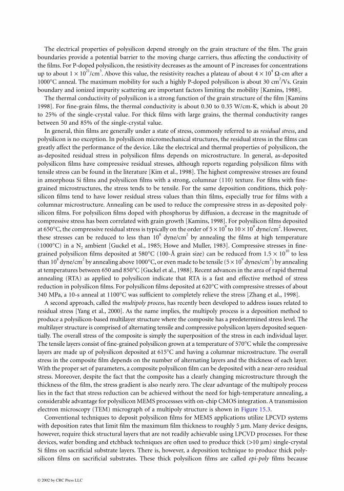
The electrical properties of polysilicon depend strongly on the grain structure of the film. The grainboundaries provide a potential barrier to the moving charge carriers, thus affecting the conductivity ofthe films. For P-doped polysilicon, the resistivity decreases as the amount of P increases for concentrationsup to about 1 × 10
21/cm
3. Above this value, the resistivity reaches a plateau of about 4 × 10
4 Ω-cm after a
1000°C anneal. The maximum mobility for such a highly P-doped polysilicon is about 30 cm2/Vs. Grain
boundary and ionized impurity scattering are important factors limiting the mobility [Kamins, 1988].The thermal conductivity of polysilicon is a strong function of the grain structure of the film [Kamins
1998]. For fine-grain films, the thermal conductivity is about 0.30 to 0.35 W/cm-K, which is about 20to 25% of the single-crystal value. For thick films with large grains, the thermal conductivity rangesbetween 50 and 85% of the single-crystal value.
In general, thin films are generally under a state of stress, commonly referred to as residual stress, andpolysilicon is no exception. In polysilicon micromechanical structures, the residual stress in the films cangreatly affect the performance of the device. Like the electrical and thermal properties of polysilicon, theas-deposited residual stress in polysilicon films depends on microstructure. In general, as-depositedpolysilicon films have compressive residual stresses, although reports regarding polysilicon films withtensile stress can be found in the literature [Kim et al., 1998]. The highest compressive stresses are foundin amorphous Si films and polysilicon films with a strong, columnar (110) texture. For films with fine-grained microstructures, the stress tends to be tensile. For the same deposition conditions, thick poly-silicon films tend to have lower residual stress values than thin films, especially true for films with acolumnar microstructure. Annealing can be used to reduce the compressive stress in as-deposited poly-silicon films. For polysilicon films doped with phosphorus by diffusion, a decrease in the magnitude ofcompressive stress has been correlated with grain growth [Kamins, 1998]. For polysilicon films depositedat 650°C, the compressive residual stress is typically on the order of 5 × 10
9 to 10 × 10
9 dyne/cm
2. However,
these stresses can be reduced to less than 108 dyne/cm
2 by annealing the films at high temperature
(1000°C) in a N2 ambient [Guckel et al., 1985; Howe and Muller, 1983]. Compressive stresses in fine-grained polysilicon films deposited at 580°C (100-Å grain size) can be reduced from 1.5 × 10
10 to less
than 108 dyne/cm
2 by annealing above 1000°C, or even made to be tensile (5 × 10
9 dynes/cm
2) by annealing
at temperatures between 650 and 850°C [Guckel et al., 1988]. Recent advances in the area of rapid thermalannealing (RTA) as applied to polysilicon indicate that RTA is a fast and effective method of stressreduction in polysilicon films. For polysilicon films deposited at 620°C with compressive stresses of about340 MPa, a 10-s anneal at 1100°C was sufficient to completely relieve the stress [Zhang et al., 1998].
A second approach, called the multipoly process, has recently been developed to address issues related toresidual stress [Yang et al., 2000]. As the name implies, the multipoly process is a deposition method toproduce a polysilicon-based multilayer structure where the composite has a predetermined stress level. Themultilayer structure is comprised of alternating tensile and compressive polysilicon layers deposited sequen-tially. The overall stress of the composite is simply the superposition of the stress in each individual layer.The tensile layers consist of fine-grained polysilicon grown at a temperature of 570°C while the compressivelayers are made up of polysilicon deposited at 615°C and having a columnar microstructure. The overallstress in the composite film depends on the number of alternating layers and the thickness of each layer.With the proper set of parameters, a composite polysilicon film can be deposited with a near-zero residualstress. Moreover, despite the fact that the composite has a clearly changing microstructure through thethickness of the film, the stress gradient is also nearly zero. The clear advantage of the multipoly processlies in the fact that stress reduction can be achieved without the need for high-temperature annealing, aconsiderable advantage for polysilicon MEMS processses with on-chip CMOS integration. A transmissionelectron microscopy (TEM) micrograph of a multipoly structure is shown in Figure 15.3.
Conventional techniques to deposit polysilicon films for MEMS applications utilize LPCVD systemswith deposition rates that limit film the maximum film thickness to roughly 5 µm. Many device designs,however, require thick structural layers that are not readily achievable using LPCVD processes. For thesedevices, wafer bonding and etchback techniques are often used to produce thick (>10 µm) single-crystalSi films on sacrificial substrate layers. There is, however, a deposition technique to produce thick poly-silicon films on sacrificial substrates. These thick polysilicon films are called epi-poly films because
© 2002 by CRC Press LLC

epitaxial Si reactors are used to deposit these films using a high-temperature process. Unlike conventionalLPCVD polysilicon deposition processes which have deposition rates of 100 Å/min, epi-poly processeshave deposition rates on the order of 1 µm/min [Gennissen et al., 1997]. The high deposition rates area result of the deposition conditions used—specifically, much higher substrate temperatures (>1000°C) anddeposition pressures (>50 torr). The polysilicon films are usually deposited on SiO2 sacrificial substratelayers and have been used in the fabrication of mechanical properties test structures [Lange et al., 1996;Gennissen et al., 1997; Greek et al., 1999], thermal actuators [Gennissen et al., 1997], electrostaticallyactuated accelerometers [Gennissen et al., 1997] and gryoscopes [Funk et al., 1999]. An LPCVD polysil-icon seed layer is used in order to control nucleation, grain size and surface roughness. In general, themicrostructure and residual stress of epi-poly films is related to deposition conditions, with compressivefilms having a mixture of (110) and (311) grains [Lange et al., 1996; Greek et al., 1999] and tensile filmshaving a random mix of (110), (100), (111) and (311) grains [Lange et al., 1996]. The Young’s modulusof epi-poly measured from micromachined test structures is comparable to LPCVD polysilicon [Greeket al., 1999].
Porous Si is a “type” of Si finding applications in MEMS technology. Porous Si is made by room-temperature electrochemical etching of Si in HF. Under normal conditions, Si is not etched by HF, henceits widespread use as an etchant of sacrificial oxide in polysilicon surface micromachining. In an elec-trochemical circuit using an HF-based solution, however, positive charge carriers (holes) at the Si surfacefacilitate the exchange of F atoms with the H atoms terminating the Si surface bonds. The exchangecontinues with the exchange of subsurface bonds, leading to the eventual removal of the fluorinated Si.The quality of the etched surface is related to the density of holes at the surface which is controlled bythe applied current density. For high current densities, the density of holes is high and the etched surfaceis smooth. For low current density, the density of holes is low and they are clustered in highly localizedregions associated with surface defects. The surface defects become enlarged by etching, leading to theformation of pores. Pore size and density are related to the type of Si used and the conditions of theelectrochemical cell. Both single-crystal and polycrystalline Si can be converted to porous Si, withporosities of up to 80% possible.
The large surface-to-volume ratios make porous Si attractive for many MEMS applications. As onemight expect, use of porous Si has been proposed for a number of gaseous and liquid applications,including filter membranes and absorbing layers for chemical and mass sensing [Anderson et al., 1994].The large surface-to-volume ratio also permits the use of porous Si as the starting material for the formation
FIGURE 15.3 TEM micrograph of a polysilicon multilayer film created using the multipoly process.
© 2002 by CRC Press LLC
of thick thermal oxides, as the proper pore size can be selected to account for the volume expansion ofthe thermal oxide. When single-crystal substrates are used in the formation of porous Si films, the unetchedmaterial remains single crystalline, thus providing the appropriate template for epitaxial growth. It hasbeen shown that CVD coatings will not penetrate the porous regions, but rather overcoat the pores at thesurface [Lang et al., 1995]. The formation of localized, surface-micromachinable, Si on insulator structuresis possible by simply combining electrochemical etching, epitaxial growth, dry etching (to create accessholes) and thermal oxidation. A third, MEMS-related application is the direct use of porous Si as a sacrificiallayer in polysilicon and single-crystalline Si surface micromachining. The process involves the electricalisolation of the structural Si layer either by the formation of pn-junctions through selective doping or byuse of electrically insulating thin films [Lang, 1995]. In essence the formation of pores only occurs onelectrically charged surfaces. A weak Si etchant aggressively attacks the porous regions with little damageto the structural Si layers. Porous Si may be an attractive option for micromachining processes that arechemically stable in HF but are tolerant of high-temperature processing steps.
With the possible exception of porous Si, all of the above-mentioned processes to prepare polysiliconfor MEMS applications utilize substrate temperatures in excess of 570°C, either during film depositionor in subsequent stress-relieving annealing steps. Such high-temperature processing restricts the use ofnon-Si derivative materials, such as aluminum for metallization and polymers for sacrificial layers, bothof which are relatively straightforward to deposit and pattern and would be of great benefit to polysiliconmicromachining if they could be used throughout the process. Work in developing low-temperaturedeposition processes for polysilicon has focused on sputter deposition techniques [Abe and Reed, 1996;Honer and Kovacs, 2000]. Early work [Abe and Reed, 1996] emphasized the ability to deposit very smooth(25-Å roughness average) films at reasonable deposition rates (191 Å/min) and with low residual com-pressive stresses. The process involved DC magnitron sputtering from a Si target using an Ar sputteringgas, a chamber pressure of 5 mtorr and a power of 100 W. The substrates consisted of thermally oxidizedSi wafers. The authors reported that a post-deposition anneal at 700°C in N2 for 2 hr was performed tocrystallize the deposited film and perhaps lower the stress. A second group [Honer and Kovacs, 2000]sought to develop a polymer-friendly, Si-based, surface-micromachining process. The Si films were sputter-deposited on polyimide sacrificial layers. To improve the conductivity of the micromachined Si struc-tures, the sputtered Si films were sandwiched between two TiW cladding layers. The device structureswere released by etching the polyimide in a O2 plasma. The processing step with the highest temperaturewas the polyimide cure, which was performed for 1 hr at 350°C. To test the robustness of the process,sputter-deposited Si microstructures were fabricated on substrates containing CMOS devices. Asexpected from thermal budget considerations, the authors reported no measurable degradation of deviceperformance.
15.4 Silicon Dioxide
SiO2 can be grown thermally on Si substrates as well as also deposited using a variety of processes to satisfya wide range of different requirements. In polysilicon surface micromachining, SiO2 is used as a sacrificialmaterial, as it can be easily dissolved using etchants that do not attack polysilicon. In a less prominent role,SiO2 is used as an etch mask for dry etching of thick polysilicon films, as it is chemically resistant to drypolysilicon etch chemistries.
The SiO2 growth and deposition processes most widely used in polysilicon surface micromachiningare thermal oxidation and LPCVD. Thermal oxidation of Si is performed at high temperatures (e.g., 900to 1000°C) in the presence of oxygen or steam. Because thermal oxidation is a self-limiting process (i.e.,the oxide growth rate decreases with increasing film thickness), the maximum practical film thicknessthat can be obtained is about 2 µm, which for many sacrificial applications is sufficient.
SiO2 films for MEMS applications can also be deposited using an LPCVD process known as low-temperature oxidation (LTO). In general, LPCVD provides a means for depositing thick (>2 µm) SiO2
films at temperatures much lower than thermal oxidation. Not only are LTO films deposited at lowtemperatures, but the films also have a higher etch rate in HF than thermal oxides which results in
© 2002 by CRC Press LLC

significantly faster releases of polysilicon surface-micromachined devices. An advantage of the LPCVDprocesses is that dopant gases can be included in the flow of source gases in order to dope the as-depositedSiO2 films. One such example is the incorporation of P to form phosphosilicate glass (PSG). PSG isformed using the same deposition process as LTO, with PH3 added to dope the glass with a P contentranging from 2 to 8 wt%. PSG has an even higher etch rate in HF than LTO, further facilitating therelease of polysilicon surface-micromachined components. PSG flows at high temperatures (e.g., 1000to 1100°C) which can be exploited to create a smooth surface topography. Additionally, PSG layerssandwiching a polysilicon film can be used as a P doping source, improving the uniformity of diffusion-based doping.
Phosphosilicate glass and LTO films are deposited in hot-wall, low-pressure, fused-silica reactors in amanner similar to the systems described previously for polysilicon. Typical deposition rates are about100 Å/min. Precursor gases include SiH4 as a Si source, O2 as an oxygen source and, in the case of PSG,PH3 as a source of phosphorus. Because SiH4 is pyrophoric (i.e., spontaneously combusts in the presenceof O2), door injection of the deposition gases would result in a large depletion of the gases at depositiontemperatures of 400 to 500°C and nonuniform deposition along the tube. Therefore, the gases areintroduced in the furnace through injectors distributed along the length of the tube. The wafers areplaced vertically in caged boats to ensure uniform gas transport to the wafers. In the caged boats, twowafers are placed back to back in each slot, thus minimizing the deposition of SiO2 on the back of thewafers. The typical load of an LTO system is over 100 wafers.
Low-temperature oxidation and PSG films are typically deposited at temperatures of 425 to 450°Cand pressures ranging from 200 to 400 mtorr. The low deposition temperatures result in LTO and PSGfilms that are slightly less dense than thermal oxides due to incorporation of hydrogen in the films. LTOfilms can, however, be densified by an annealing step at high temperature (1000°C). The low densityof LTO and PSG films is partially responsible for the increased etch rate in HF, which makes themattractive sacrificial materials for polysilicon surface micromachining. LTO and PSG deposition pro-cesses are not typically conformal to nonplanar surfaces because the low substrate temperatures resultin low surface migration of reacting species. Step coverage is, however, sufficient for many polysiliconsurface-micromachining applications, although deposited films tend to thin at the bottom surfaces ofdeep trenches and therefore must be thoroughly characterized for each application.
The dissolution of the sacrificial SiO2 to release free-standing structures is a critical step in polysiliconsurface micromachining. Typically, 49% (by weight) HF is used for the release process. To pattern oxidefilms using wet chemistries, etching in buffered HF (28 ml 49% HF, 170 ml H2O, 113 g NH4F), alsoknown as buffered oxide etch (BOE), is common for large structures. A third wet etchant, known asP-etch, is traditionally used to selectively remove PSG over undoped oxide (e.g., to deglaze a wafer straightfrom a diffusion furnace).
Thermal SiO2, LTO, and PSG are electrical insulators suitable for many MEMS applications. Thedielectric constants of thermal oxide and LTO are 3.9 and 4.3, respectively. The dielectric strength ofthermal SiO2 is 1.1 × 10
6 V/cm, and for LTO it is about 80% that of thermal SiO2 [Ghandhi, 1983].
Thermal SiO2 is in compression with a stress level of about 3 × l09 dyne/cm
2 [Ghandhi, 1983]. For LTO,
however, the as-deposited residual stress is tensile, with a magnitude of about 1 to 4 × 10⁹ dyne/cm
2
[Ghandhi, 1983]. The addition of phosphorous to LTO (i.e., PSG) decreases the tensile residual stress toabout 10
8 dyne/cm
2 for a phosphorus concentration of 8% [Pilskin, 1977]. These data are representative
of oxide films deposited directly on Si substrates under typical conditions; however, the final value ofthe stress in an oxide film can be a strong function of the process parameters as well as any post-processing steps.
A recent report documents the development of another low-pressure process, known as plasma-enhanced chemical vapor deposition (PECVD), for MEMS applications. The objective was to depositlow-stress, very thick (10 to 20 µm) SiO2 films for insulating layers in micromachined gas turbine engines[Zhang et al., 2000]. PECVD was selected, in part, because it offers the possibility to deposit films of thedesired thickness at a reasonable deposition rate. The process used a conventional parallel plate reactorwith tetraethylorthosilicate (TEOS), a commonly used precursor in LPCVD processes, as the source gas.
© 2002 by CRC Press LLC

As expected, the authors found that film stress is related to the concentration of dissolved gases in thefilm and that annealed films tend to suffer from cracking. By using a thin Si3N4 film in conjunction withthe thick SiO2 film, conditions were found where a low-stress, crack-free SiO2 film could be produced.
Two other materials in the SiO2 family are receiving increasing attention from MEMS fabricators,especially now that the material systems have expanded beyond conventional Si processing. The first ofthese is crystalline quartz. The chemical composition of quartz is SiO2. Quartz is optically transparentand, like its amorphous counterpart, quartz is electrically insulating. However, the crystalline nature ofquartz gives it piezoelectric properties that have been exploited for many years in electronic circuitry. Likesingle-crystal Si, quartz substrates are available as high-quality, large-area wafers. Also like single-crystalSi, quartz can be bulk micromachined using anisotropic etchants based on heated HF and ammoniumfluoride (NH4F) solutions, albeit the structural shapes that can be etched into quartz do not resemble theshapes that can be etched into Si. A short review of the basics of quartz etching and its applications to thefabrication of a micromachined acceleration sensor can be found in Danel et al. (1990).
A second SiO2-related material that has found utility in MEMS is spin-on-glass (SOG), which is usedin thin-film form as a planarization dielectric material in IC processing. As the name implies, SOG isapplied to a substrate by spin coating. The material is polymer based with a viscosity suitable for spin-coating, and once dispensed at room temperature on the spinning substrate, it is cured at elevatedtemperatures to form a solid thin film. Two recent publications illustrate the potential uses of SOG inMEMS. In the first example, SOG was developed as a thick-film sacrificial molding material to patternthick polysilicon films [Yasseen et al., 1999]. The authors reported a process to produce SOG films thatwere 20 µm thick, complete with a chemical–mechanical polishing (CMP) procedure and etching tech-niques. The thick SOG films were patterned into molds that were filled with 10-µm-thick LPCVDpolysilicon films, planarized by selective CMP and subsequently dissolved in a HCl:HF:H2O wet etchantto reveal the patterned polysilicon structures. The cured SOG films were completely compatible with thepolysilicon deposition process, indicating that SOG could be used to produce MEMS devices withextremely large gaps between structural layers. In the second example, high-aspect-ratio channel-platemicrostrucures were fabricated from SOG [Liu et al., 1999]. The process required the use of molds tocreate the structures. Electroplated nickel (Ni) was used as the molding material, with Ni channel platemolds fabricated using a conventional LIGA process. The Ni molds are then filled with SOG, and thesacrificial Ni molds are removed in a reverse electroplating process. In this case, the fabricated SOGstructures were over 100 µm tall, essentially bulk micromachined structures fabricated using a sacrificialmolding material system.
15.5 Silicon Nitride
Si3N4 is widely used in MEMS for electrical isolation, surface passivation, etch masking and as a mechan-ical material. Two deposition methods are commonly used to deposit Si3N4 thin films: LPCVD andPECVD. PECVD Si3N4 is generally nonstoichiometric and may contain significant concentrations ofhydrogen. Use of PECVD Si3N4 in micromachining applications is somewhat limited because its etchrate in HF can be high (e.g., often higher than that of thermally grown SiO2) due to the porosity of thefilm. However, PECVD offers the potential to deposit nearly stress-free Si3N4 films, an attractive propertyfor many MEMS applications, especially in the area of encapsulation and packaging. Unlike its PECVDcounterpart, LPCVD Si3N4 is extremely resistant to chemical attack, thereby making it the material ofchoice for many Si bulk and surface micromachining applications. LPCVD Si3N4 is commonly used asan insulating layer to isolate device structures from the substrate and from other device structures, becauseit is a good insulator with a resistivity of 10
16 Ω-cm and a field breakdown limit of 10
7 V/cm.
The LPCVD Si3N4 films are deposited in horizontal furnaces similar to those used for polysilicondeposition. Typical deposition temperatures and pressures range between 700 and 900°C and 200 to 500mtorr, respectively. A typical deposition rate is about 30 Å/min. The standard source gases are dichlo-rosilane (SiH2Cl2) and ammonia (NH3). SiH2Cl2 is used in place of SiH4 because it produces films witha higher degree of thickness uniformity at the required deposition temperature and it allows the wafers
© 2002 by CRC Press LLC
to be spaced close together, thus increasing the number of wafers per furnace load. To produce stoichi-ometric Si3N4, a NH3-to-SiH2Cl2 ratio of 10:1 is commonly used. The standard furnace configurationuses door injection of the source gases with a temperature gradient along the tube axis to accommodatefor the gas depletion effects. LPCVD Si3N4 films deposited between 700 and 900°C are amorphous;therefore, the material properties do not vary significantly along the length of tube despite the temperaturegradient. As with polysilicon deposition, a typical furnace can accommodate over 100 wafers. BecauseSi3N4 is deposited in the reaction-limited regime, film is deposited on both sides of each wafer with equalthickness.
The residual stress in stochiometric Si3N4 is large and tensile, with a magnitude of about 1010
dyne/cm2.
Such a large residual stress limits the practical thickness of a deposited Si3N4 film to a few thousandangstroms because thicker films tend to crack. Nevertheless, stoichiometric Si3N4 films have been usedas mechanical support structures and electrical insulating layers in piezoresistive pressure sensors[Folkmer et al., 1995]. To reduce the residual stress, thus enabling the use of thick Si3N4 films forapplications that require durable, chemically resistant membranes, nonstoichiometric silicon nitride(SixNy) films can be deposited by LPCVD. These films, often referred to as Si-rich or low-stress nitride,are intentionally deposited with an excess of Si by simply decreasing the NH3 to SiH2Cl2 ratio in thereaction furnace. For a NH3-to-SiH2Cl2 ratio of 1:6 at a deposition temperature of 850°C and pressureof 500 mtorr, the as-deposited films are nearly stress free [Sekimoto et al., 1982]. The increase in Sicontent not only leads to a reduction in tensile stress, but also decreases the etch rate of the film in HF.As a result, low-stress silicon nitride films have replaced stoichiometric Si3N4 in many MEMS applicationsand even have enabled the development of fabrication techniques that would otherwise not be feasiblewith stoichiometric Si3N4. For example, low-stress silicon nitride has been successfully used as a structuralmaterial in a surface micromachining process that uses polysilicon as the sacrificial material [Monk et al.,1993]. In this case, Si anisotropic etchants such as KOH and EDP were used for dissolving the sacrificialpolysilicon. A second low-stress nitride surface micromachining process used PSG as a sacrificial layer,which was removed using a HF-based solution [French et al., 1997]. Of course, wide use of Si3N4 as aMEMS material is restricted by its dielectric properties; however, its Young’s modulus (146 GPa) is onpar with Si (∼190 GPa), making it an attractive material for mechanical components.
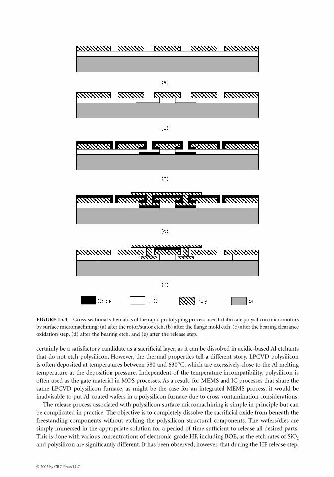
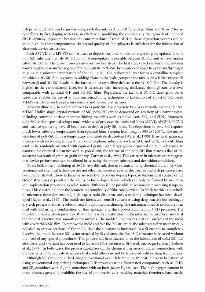
The essential interactions between substrate, electrical isolation layer, sacrificial layers, and structurallayers are best illustrated by examining the critical steps in a multilevel surface micromachining process.The example used here (shown in Figure 15.4) is the fabrication of a Si micromotor using a techniquecalled the rapid prototyping process. The rapid prototyping process utilizes three deposition and threephotolithography steps to implement flange-bearing, side-drive micromotors such as in the SEM ofFigure 15.5. The device consists of heavily P-doped LPCVD polysilicon structural components depositedon a Si wafer, using LTO both as a sacrificial layer and as an electrical isolation layer. Initially, a 2.4-µm-thick LTO film is deposited on the Si substrate. A 2-µm-thick doped polysilicon layer is then depositedon the LTO film. Photolithography and RIE steps are then performed to define the rotor, stator androtor/stator gap. To fabricate the flange, a sacrificial mold is created by etching into the LTO film withan isotropic etchant, then partially oxidizing the polysilicon rotor and stator structures to form what iscalled the bearing clearance oxide. This oxidation step also forms the bottom of the bearing flange mold.A 1- to 2-µm-thick, heavily doped polysilicon film is then deposited and patterned by photolithographyand RIE to form the bearing. At this point, the structural components of the micromotor are completelyformed, and all that remains is to release the rotor by etching the sacrificial oxide in HF and performingan appropriate drying procedure (detailed later in this chapter). In this example, the LTO film servesthree purposes: It is the sacrificial underlayer for the free-spinning rotor, it comprises part of the flangemold, and it serves as an insulating anchor for the stators and bearing post. Likewise, the thermal oxideserves as a mold and electrical isolation layer. The material properties of LTO and thermal oxide allowfor these films to be used as they are in the rapid prototyping process, thus enabling the fabrication ofmultilayer structures with a minimum of processing steps.
Without question, SiO2 is an excellent sacrificial material for polysilicon surface micromachining;however, other materials could also be used. In terms of chemical properties, aluminum (Al) would
© 2002 by CRC Press LLC
certainly be a satisfactory candidate as a sacrificial layer, as it can be dissolved in acidic-based Al etchantsthat do not etch polysilicon. However, the thermal properties tell a different story. LPCVD polysiliconis often deposited at temperatures between 580 and 630°C, which are excessively close to the Al meltingtemperature at the deposition pressure. Independent of the temperature incompatibility, polysilicon isoften used as the gate material in MOS processes. As a result, for MEMS and IC processes that share thesame LPCVD polysilicon furnace, as might be the case for an integrated MEMS process, it would beinadvisable to put Al-coated wafers in a polysilicon furnace due to cross-contamination considerations.
The release process associated with polysilicon surface micromachining is simple in principle but canbe complicated in practice. The objective is to completely dissolve the sacrificial oxide from beneath thefreestanding components without etching the polysilicon structural components. The wafers/dies aresimply immersed in the appropriate solution for a period of time sufficient to release all desired parts.This is done with various concentrations of electronic-grade HF, including BOE, as the etch rates of SiO2
and polysilicon are significantly different. It has been observed, however, that during the HF release step,
FIGURE 15.4 Cross-sectional schematics of the rapid prototyping process used to fabricate polysilicon micromotorsby surface micromachining: (a) after the rotor/stator etch, (b) after the flange mold etch, (c) after the bearing clearanceoxidation step, (d) after the bearing etch, and (e) after the release step.
© 2002 by CRC Press LLC

the mechanical properties of polysilicon, including residual stress, Young’s modulus and fracture strain,can be affected [Walker et al., 1991]. In general, the modulus and fracture strain of polysilicon decreaseswith increasing time of exposure to HF and with increasing HF concentration. This decrease in themodulus and fracture strain indicates a degradation of the film mechanical integrity. To minimize theHF release time, structures are designed with access holes and cuts of sufficient size to facilitate the flowof HF to the sacrificial oxide. In this manner, polysilicon structures can be released without appreciabledegradation to film properties and hence device performance.
Following the HF release step, the devices must be rinsed and dried. A simple process includes rinsesin deionized (DI) water then in methanol, followed by a drying step using N2. The primary difficultywith the wet release process is that surface tension forces, which are related to the surface properties ofthe material, tend to pull the micromechanical parts toward the substrate as the devices are immersedand pulled out of the solutions. Release processes that avoid the surface tension problem by using frozenalcohols that are sublimated at the final rinse step have been developed [Guckel et al., 1990]. Processesbased on the use of supercritical fluids [Mulhern et al., 1993], such as CO2 at 35°C and 1100 psi, toextinguish surface tension effects vanish are now commonplace in many MEMS facilities.
15.6 Germanium-Based Materials
Germanium (Ge) has a long history in the development of semiconducting materials, dating back to thedevelopment of the earliest transistors. The same is true in the development of micromachined trans-ducers and the early work on the piezoresistive effect in semiconducting materials [Smith, 1954]. Devel-opment of Ge for microelectronic devices may have continued if only a water-insoluable oxide could beformed on Ge surfaces. Nonetheless, there is a renewed interest in Ge for micromachined devices,especially for devices that require use of low-temperature processes.
Thin polycrystalline Ge (poly-Ge) films can be deposited by LPCVD at temperatures much lower thanpolysilicon, namely, 325°C at a pressure of 300 mtorr on Si, Ge or SiGe substrates [Li et al., 1999]. Gedoes not nucleate on SiO2 surfaces, which prohibits use of thermal oxides and LTO films as sacrificialsubstrate layers but does enable use of these films as sacrificial molds, as selective growth using SiO2
masking films is possible. Residual stress in poly-Ge films deposited on Si substrates is about 125 MPacompressive, which can be reduced to nearly zero after a 30-s anneal at 600°C. Poly-Ge is essentiallyimpervious to KOH, tetramethyl ammonium hydroxide (TMAH) and BOE, making it an ideal maskingand etch-stop material in Si micromachining. In fact, the combination of low residual stress and inertnessto Si anisotropic etches enables the fabrication of Ge membranes on Si substrates [Li et al., 1999]. Themechanical properties of poly-Ge are comparable with polysilicon, with a Young’s modulus measured at
FIGURE 15.5 SEM micrograph of a polysilicon micromotor fabricated using the rapid prototyping process.
© 2002 by CRC Press LLC

132 GPa and a fracture stress ranging between 1.5 GPa and 3.0 GPa [Franke et al., 1999]. Poly-Ge can alsobe used as a sacrificial layer. Typical wet etchants are based on mixtures of HNO3, H2O and HCl and H2O,H2O2 and HCl, as well as the RCA SC-1 cleaning solution. These mixtures do not etch Si, SiO2, Si3N4 andSixNy , thereby enabling the use of poly-Ge as a sacrificial substrate layer in polysilicon surface micro-machining. Using the above-mentioned techniques, poly-Ge-based thermistors and Si3N4-membrane-based pressure sensors using poly-Ge sacrificial layers have been fabricated [Li et al., 1999]. In addition,poly-Ge microstructures, such as lateral resonant structures, have been fabricated on Si substrates containingCMOS structures with no process-related degradation in performance, thus showing the advantages of lowdeposition temperatures and compatible wet chemical etching techniques [Franke et al., 1999].
SiGe is an alloy of Si and Ge and has recently received attention for its usefulness in microelectronics;therefore, deposition technologies for SiGe thin films are readily available. While the requirements forSiGe-based electronic devices require single-crystal material, the requirements for MEMS are much lessrestrictive, allowing for the use of polycrystalline material in many applications. Polycrystalline SiGe(poly-SiGe) films retain many properties comparable to polysilicon but can be deposited at lower substratetemperatures. Deposition processes include LPCVD, atmospheric pressure chemical vapor deposition(APCVD) and RTCVD (rapid thermal CVD) using SiH4 and GeH4 as precursor gases. Deposition temp-erature range from 450°C for LPCVD [Franke et al., 2000] to 625°C for RTCVD [Sedky et al., 1998].The LPCVD processes can be performed in horizontal furnace tubes similar in configuration and size tothose used for the deposition of polyslicon films. In general, the deposition temperature is related to theconcentration of Ge in the films, with higher Ge concentration resulting in lower deposition temperatures.Like polysilicon, poly-SiGe can be doped with B and P to modify its conductivity. In fact, it has been reportedthat as-deposited, in situ, B-doped poly-SiGe films have a resistivity of 1.8 mΩ-cm [Franke et al., 2000].
Poly-SiGe can be deposited on a number of sacrificial substrates, including SiO2 [Sedky et al., 1998],PSG [Franke et al., 1999] and poly-Ge [Franke et al., 1999], which, as detailed in previous sections ofthis chapter, can also be deposited at relatively low processing temperatures. For films rich in Ge, a thinpolysilicon seed layer is sometimes used on SiO2 surfaces, as Ge does not readily nucleate on oxide surfaces.Because poly-SiGe is an alloy, variations in film stoichiometry can result in changes in physical properties.For instance, attack of poly-SiGe by H2O2, a main component in some Ge etchants, becomes problematicfor Ge concentrations over 70%. As with most CVD thin films, residual stress is dependent on thesubstrate used and the deposition conditions; however, for in situ B-doped films, the as-deposited stressesare quite low at 10 MPa compressive [Franke et al., 2000].
In many respects, fabrication of devices made from poly-SiGe thin films follows processing methods usedin polysilicon micromachining, as Si and Ge are quite compatible. The poly-SiGe/poly-Ge material systemis particularly attractive for surface micromachining, as it is possible to use H2O2 as a release agent. It hasbeen reported that in H2O2, poly-Ge etches at a rate of 0.4 µm/min, while poly-SiGe with Ge concentrationsbelow 80% have no observable etch rate after 40 hr [Heck et al., 1999]. The ability to use H2O2 as a sacrificialetchant makes the poly-SiGe and poly-Ge combination perhaps the ideal material system for surfacemicromachining. To this end, several interesting devices have been fabricated from poly-SiGe. Due to theconformal nature of the poly-SiGe coating, poly-SiGe-based, high-aspect-ratio structural elements, such asgimbal/microactuator structures made using the Hexil process [Heck et al., 1999], can readily be fabricated.Capitalizing on the low substrate temperatures associated with the deposition of poly-SiGe and poly-Ge thinfilms, an integrated MEMS fabrication process on Si wafers has been demonstrated [Franke et al., 2000]. Inthis process, CMOS structures are first fabricated into standard Si wafers. Poly-SiGe thin-film mechanicalstructures are surface micromachined atop the CMOS devices using a poly-Ge sacrificial layer and H2O2 asan etchant. A significant advantage of this design lies in the fact that the MEMS structure is positioned directlyabove the CMOS structure, thus significantly reducing the parasitic capacitance and contact resistancecharacteristic of interconnects associated with the side-by-side integration schemes often used in integratedpolysilicon MEMS. Use of H2O2 as the sacrificial etchant means that no special protective layers are requiredto protect the underlying CMOS layer during release. Clearly, the unique properties of the poly-SiGe/poly-Ge material system, used in conjunction with the Si/SiO2 material system, enable fabrication of inte-grated MEMS that minimizes interconnect distances and potentially increases device performance.
© 2002 by CRC Press LLC

15.7 Metals
Metals are used in many different capacities, ranging from hard etch masks and thin film conductinginterconnects to structural elements in microsensors and microactuators. Metallic thin films can bedeposited using a wide range of deposition techniques, the most common being evaporation, sputtering,CVD and electroplating. Such a wide range of deposition methods makes metal thin films one of themost versatile classes of materials used in MEMS devices. A complete review would constitute a chapterin itself; the following illustrative examples are included to give the reader an idea of how different metalthin films can be used.
Aluminum (Al) is probably the most widely used metal in micrfabricated devices. In MEMS, Al thinfilms can be used in conjunction with polymers such as polyimide because the films can be sputter-deposited at low temperatures. In most cases, Al is used as a structural layer; however, Al can be used asa sacrificial layer, as well. The polyimide/aluminum combination as structural and sacrificial materials,respectively, has also been demonstrated to be effective for surface micromachining [Schmidt et al., 1988;Mahadevan et al., 1990]. In this case, acid-based Al etchants can be used to dissolve the Al sacrificiallayer. A unique feature of this material system is that polyimide is significantly more compliant thanpolysilicon and silicon nitride (e.g., its elastic modulus is nearly 50 times smaller). At the same time,polyimide can withstand large strains (up to 100% for some chemistries) before fracture. Finally, becauseboth polyimide and Al can be processed at low temperatures (e.g., below 400°C), this material systemcan be used subsequent to the fabrication of ICs on the wafer. A drawback of polyimide is its viscoelasticproperties (i.e., it creeps).
Tungsten (deposited by CVD) as a structural material and silicon dioxide as a sacrificial material havealso been used for surface micromachining [Chen and MacDonald, 1991]. In this case, HF is used forremoving the sacrificial oxide. In conjunction with high-aspect-ratio processes, nickel and copper arebeing used as structural layers with polyimide and other metals (e.g., chromium) as the sacrificial layers.The study of many of these material systems has been either limited or is just in the preliminary stages;as a result, their benefits are yet to be determined.
Metal thin films are among the most versatile MEMS materials, as alloys of certain metallic elementsexhibit a behavior known as the shape-memory effect. The shape-memory effect relies on the reversibletransformation from a ductile martensite phase to a stiff austenite phase upon the application of heat.The reversible nature of this phase change allows the shape-memory effect to be used as an actuationmechanism. Moreover, it has been found that high forces and strains can be generated from shape-memorythin films at reasonable power inputs, thus enabling shape memory actuation to be used in MEMS-basedmicrofluidic devices such as microvalves and micropumps. Alloys of Ti and Ni, collectively known as TiNi,are among the most popular shape-memory alloys owing to their high actuation work densities (reportedto be up to 50 MJ/m
3) and large bandwidth (up to 0.1 kHz) [Shih et al., 2001]. TiNi is also attractive
because conventional sputtering techniques can be employed to deposit thin films of the alloy, as detailedin a recent report [Shih et al., 2001]. In this study, TiNi films deposited by two methods—co-sputteringelemental Ti and Ni targets and co-sputtering TiNi alloy and elemental Ti targets—were compared foruse in microfabricated shape-memory actuators. In each case, the objective was to establish conditions sothat films with the proper stoichiometry, and hence phase transition temperature, could be maintained.The sputtering tool was equipped with a substrate heater in order to deposit films on heated substratesas well as to anneal the films in vacuum after deposition. It was reported that co-sputtering from TiNiand Ti targets produced better films than co-sputtering from Ni and Ti targets, due to process variationsrelated to roughening of the Ni target. The TiNi/Ti co-sputtering process has been successfully used as anactuation material in a silicon spring-based microvalve [Hahm et al., 2000].
Use of thin-film metal alloys in magnetic actuator systems is yet another example of the versatility ofmetallic materials in MEMS. From a physical perspective, magnetic actuation is fundamentally the samein the microscopic and macroscopic domains, with the main difference being that process constraintslimit the design options of microscale devices. Magnetic actuation in microdevices generally requires themagnetic layers to be relatively thick (tens to hundreds of microns), so as to create structures that can
© 2002 by CRC Press LLC

be used to generate magnetic fields of sufficient strength to generate the desired actuation. To this end,magnetic materials are often deposited by thick-film methods such as electroplating. The thicknesses ofthese layers often exceeds what can feasibly be patterned by etching, so plating is often conducted inmicrofabricated molds usually made from X-ray-sensitive materials such as polymethylmethacrylate(PMMA). The PMMA mold thickness can exceed several hundred microns, so X-rays are used as theexposure source. In some cases, a thin-film seed layer is deposited by sputtering or other conventionalmeans before the plating process begins. At the completion of the plating process, the mold is dissolved,freeing the metallic component. This process, commonly known as LIGA, has been used to producehigh-aspect-ratio structures such as microgears from NiFe magnetic alloys [Leith and Schwartz, 1999].LIGA is not restricted to the creation of magnetic actuator structures and, in fact, has been used to makesuch structures as Ni fuel atomizers [Rajan et al., 1999]. In this application, Ni was selected for its desirablechemical, wear and temperature properties, not its magnetic properties.
15.8 Silicon Carbide
Use of Si as a mechanical and electrical material has enabled the development of MEMS for a wide rangeof applications. Of course, use of MEMS is restricted by the physical properties of the material, whichin the case of Si-based MEMS limits the devices to operating temperatures of about 200°C in low-wearand benign chemical environments. Therefore, alternate materials are necessary to extend the usefulnessof MEMS to areas classified as “harsh environments.” In a broad sense, harsh environments include allconditions where use of Si is prohibited by its electrical, mechanical and chemical properties. Thesewould include high-temperature, high-radiation, high-wear and highly acidic and basic chemical envi-ronments. To be a direct replacement for Si in such applications, the material would have to be achemically inert, extremely hard, temperature-insensitive, micromachinable semiconductor. Theserequirements pose significant fabrication challenges, as micromachining requires the use of chemical andmechanical processes to remove unwanted material. In general, a class of wide bandgap semiconductorsthat includes silicon carbide (SiC) and diamond embodies the electrical, mechanical and chemicalproperties required for many harsh environment applications, but until recently these materials foundlittle usefulness in MEMS because the necessary micromachining processes did not exist. The followingtwo sections review the development of SiC and diamond for MEMS applications.
SiC has long been recognized as a semiconductor with potential for use in high-temperature and high-power electronics. SiC is a material that is polymorphic, meaning that it exists in multiple crystallinestructures, each sharing a common stoichiometry. SiC exists in three main polytypes: cubic, hexagonaland rhombehedral. The cubic polytype, called 3C-SiC, has an electronic bandgap of 2.3 eV, which is overtwice that of Si. Numerous hexagonal and rhombehedral polytypes have been identified, the two mostcommon being the 4H-SiC and 6H-SiC hexagonal polytypes. The electronic bandgap of 4H- and 6H-SiCis even higher than 3C-SiC, being 2.9 and 3.2 eV, respectively. SiC in general has a high thermalconductivity, ranging from 3.2 to 4.9 W/cm-K, and a high breakdown field (30 × 10
5 V/cm). SiC films
can be doped to create n- and p-type material. The stiffness of SiC is quite large relative to Si, withmeasured Young’s modulus values in the range of 300 to 700 GPa, which makes it very attractive formicromachined resonators and filters, as the resonant frequency increases with increasing modulus. SiCis not etched in any wet chemistries commonly used in Si micromachining. SiC can be etched in strongbases like KOH, but only at temperatures in excess of 600°C. SiC is a material that does not melt, butrather sublimes at temperatures in excess of 1800°C. Single-crystal 4H- and 6H-SiC wafers are commer-cially available, although they are smaller (3-in. diameter) and much more expensive than Si. With thislist of properties, it is little wonder why SiC is being actively researched for MEMS applications.
SiC thin films can be grown or deposited using a number of different techniques. For high-qualitysingle-crystal films, APCVD and LPCVD processes are most commonly employed. The high crystalquality is achieved by homoepitaxial growth of 4H- and 6H-SiC films on substrates of like crystal type.These processes usually employ dual precursors to supply Si and C, with the common sources being SiH4
and C3H8. Typical epitaxial growth temperatures range from 1500 to 1700°C. Epitaxial films with p- or
© 2002 by CRC Press LLC
n-type conductivity can be grown using such dopants as Al and B for p-type films and N or P for n-type films. In fact, doping with N is so effective at modifying the conductivity that growth of undopedSiC is virtually impossible because the concentrations of residual N in these deposition systems can bequite high. At these temperatures, the crystal quality of the epilayers is sufficient for the fabrication ofelectronic device structures.
Both APCVD and LPCVD can be used to deposit the only known polytype to grow epitaxially on anon-SiC substrate, namely 3C-SiC on Si. Heteroepitaxy is possible because 3C-SiC and Si have similarlattice structures. The growth process involves two key steps. The first step, called carbonization, involvesconverting the near-surface region of the Si substrate to 3C-SiC by simply exposing it to a propane/hydrogenmixture at a substrate temperature of about 1300°C. The carbonized layer forms a crystalline templateon which a 3C-SiC film is grown by adding silane to the hydrogen/propane mix. A 20% lattice mismatchbetween Si and 3C-SiC results in the formation of crystalline defects in the 3C-SiC film. The density ishighest in the carbonization layer, but it decreases with increasing thickness, although not to a levelcomparable with epitaxial 6H- and 4H-SiC films. Regardless, the fact that 3C-SiC does grow on Sisubstrates enables the use of Si bulk micromachining techniques to fabrication of a host of SiC-basedMEMS structures such as pressure sensors and resonant structures.
Polycrystalline SiC, hereafter referred to as poly-SiC, has proven to be a very versatile material for SiCMEMS. Unlike single-crystal versions of SiC, poly-SiC can be deposited on a variety of substrate types,including common surface micromachining materials such as polysilicon, SiO2 and Si3N4. Moreover,poly-SiC can be deposited using a much wider set of processes than epitaxial films; LPCVD, APCVD, PECVDand reactive sputtering have all been used to deposit poly-SiC films. The deposition of poly-SiC requiresmuch lower substrate temperatures than epitaxial films, ranging from roughly 500 to 1200°C. The micro-structure of poly-SiC films is temperature and substrate dependent [Wu et al., 1999]. In general, grain sizeincreases with increasing temperature. For amorphous substrates such as SiO2 and Si3N4, poly-SiC filmstend to be randomly oriented with equiaxed grains, with larger grains deposited on SiO2 substrates. Incontrast, for oriented substrates such as polysilicon, the texture of the poly-SiC film matches that of thesubstrate as a result of grain-to-grain epitaxy [Zorman et al., 1996]. This variation in microstructure suggeststhat device performance can be tailored by selecting the proper substrate and deposition conditions.
Direct bulk micromachining of SiC is very difficult, due to its outstanding chemical durability. Con-ventional wet chemical techniques are not effective; however, several electrochemical etch processes havebeen demonstrated. These techniques are selective to certain doping types, so dimensional control of theetched structures depends on the ability to form doped layers, which can only be formed by in situ orion implantation processes, as solid source diffusion is not possible at reasonable processing tempera-tures. This constraint limits the geometrical complexity of fabricated devices. To fabricate thick (hundredsof microns), three-dimensional, high-aspect-ratio SiC structures, a molding technique has been devel-oped [Rajan et al., 1999]. The molds are fabricated from Si substrates using deep reactive ion etching, adry etch process that has revolutionized Si bulk micromachining. The micromachined Si molds are thenfiled with SiC using a combination of thin epitaxial and thick polycrystalline film CVD processes. Thethin-film process, which produces 3C-SiC films with a featureless SiC/Si interface, is used to ensure thatthe molded structure has smooth outer surfaces. The mold-filling process coats all surfaces of the moldwith a very thick SiC film. To remove the mold and free the SiC structure, the substrate is first mechanicallypolished to expose sections of the mold, then the substrate is immersed in a Si etchant to completelydissolve the mold. Because SiC is not attacked by Si etchants, the final SiC structure is released withoutthe need of any special procedures. This process has been successful in the fabrication of solid SiC fuelatomizers, and a variant has been used to fabricate SiC structures in Si-based, micro, gas turbines [Lohneret al., 1999]. In both cases, the process capitalizes on the chemical inertness of SiC in conjunction withthe reactivity of Si to create structures that could otherwise not be fabricated with existing technologies.
Although SiC cannot be etched using conventional wet etch techniques, thin SiC films can be patternedusing conventional dry etching techniques. RIE processes using fluorinated compounds such as CHF3
and SF6 combined with O2 and sometimes with an inert gas or H2 are used. The high oxygen content inthese plasmas generally prohibits the use of photoresist as a masking material; therefore, hard masks
© 2002 by CRC Press LLC
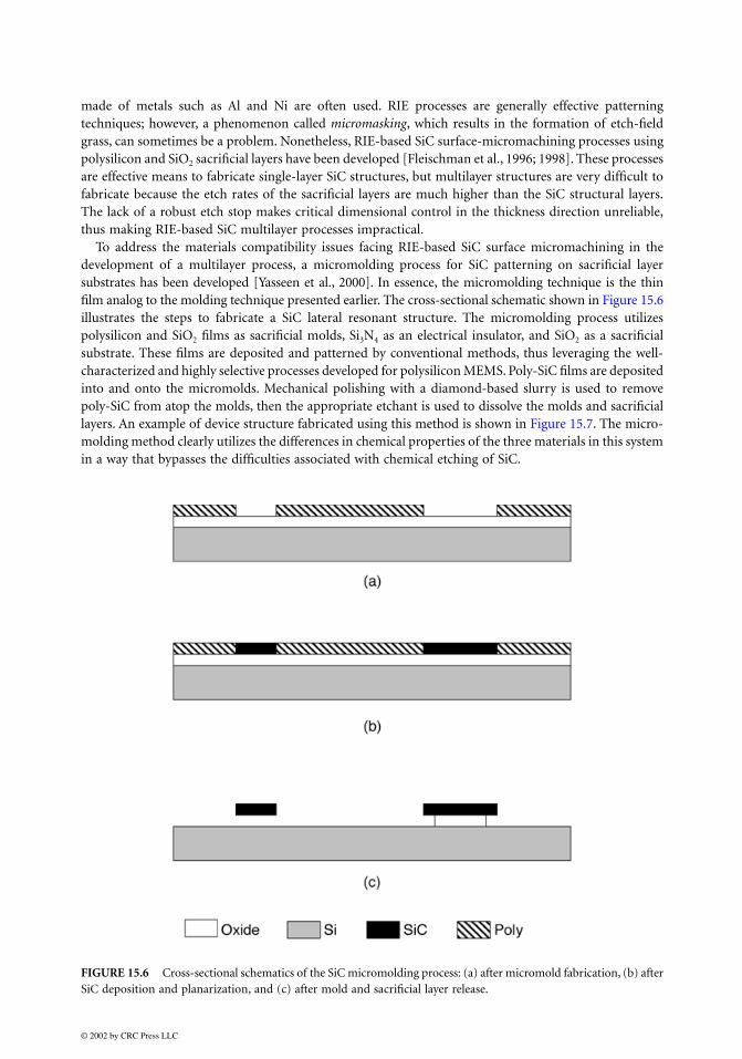
made of metals such as Al and Ni are often used. RIE processes are generally effective patterningtechniques; however, a phenomenon called micromasking, which results in the formation of etch-fieldgrass, can sometimes be a problem. Nonetheless, RIE-based SiC surface-micromachining processes usingpolysilicon and SiO2 sacrificial layers have been developed [Fleischman et al., 1996; 1998]. These processesare effective means to fabricate single-layer SiC structures, but multilayer structures are very difficult tofabricate because the etch rates of the sacrificial layers are much higher than the SiC structural layers.The lack of a robust etch stop makes critical dimensional control in the thickness direction unreliable,thus making RIE-based SiC multilayer processes impractical.
To address the materials compatibility issues facing RIE-based SiC surface micromachining in thedevelopment of a multilayer process, a micromolding process for SiC patterning on sacrificial layersubstrates has been developed [Yasseen et al., 2000]. In essence, the micromolding technique is the thinfilm analog to the molding technique presented earlier. The cross-sectional schematic shown in Figure 15.6illustrates the steps to fabricate a SiC lateral resonant structure. The micromolding process utilizespolysilicon and SiO2 films as sacrificial molds, Si3N4 as an electrical insulator, and SiO2 as a sacrificialsubstrate. These films are deposited and patterned by conventional methods, thus leveraging the well-characterized and highly selective processes developed for polysilicon MEMS. Poly-SiC films are depositedinto and onto the micromolds. Mechanical polishing with a diamond-based slurry is used to removepoly-SiC from atop the molds, then the appropriate etchant is used to dissolve the molds and sacrificiallayers. An example of device structure fabricated using this method is shown in Figure 15.7. The micro-molding method clearly utilizes the differences in chemical properties of the three materials in this systemin a way that bypasses the difficulties associated with chemical etching of SiC.
FIGURE 15.6 Cross-sectional schematics of the SiC micromolding process: (a) after micromold fabrication, (b) afterSiC deposition and planarization, and (c) after mold and sacrificial layer release.
© 2002 by CRC Press LLC
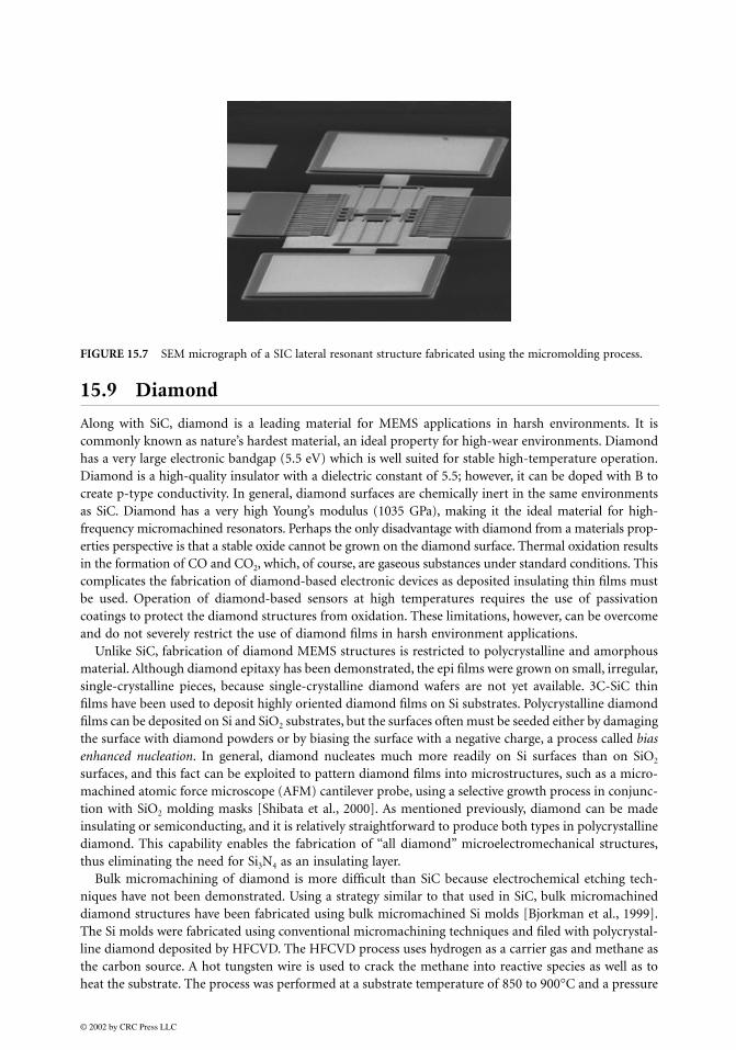
15.9 Diamond
Along with SiC, diamond is a leading material for MEMS applications in harsh environments. It iscommonly known as nature’s hardest material, an ideal property for high-wear environments. Diamondhas a very large electronic bandgap (5.5 eV) which is well suited for stable high-temperature operation.Diamond is a high-quality insulator with a dielectric constant of 5.5; however, it can be doped with B tocreate p-type conductivity. In general, diamond surfaces are chemically inert in the same environmentsas SiC. Diamond has a very high Young’s modulus (1035 GPa), making it the ideal material for high-frequency micromachined resonators. Perhaps the only disadvantage with diamond from a materials prop-erties perspective is that a stable oxide cannot be grown on the diamond surface. Thermal oxidation resultsin the formation of CO and CO2, which, of course, are gaseous substances under standard conditions. Thiscomplicates the fabrication of diamond-based electronic devices as deposited insulating thin films mustbe used. Operation of diamond-based sensors at high temperatures requires the use of passivationcoatings to protect the diamond structures from oxidation. These limitations, however, can be overcomeand do not severely restrict the use of diamond films in harsh environment applications.
Unlike SiC, fabrication of diamond MEMS structures is restricted to polycrystalline and amorphousmaterial. Although diamond epitaxy has been demonstrated, the epi films were grown on small, irregular,single-crystalline pieces, because single-crystalline diamond wafers are not yet available. 3C-SiC thinfilms have been used to deposit highly oriented diamond films on Si substrates. Polycrystalline diamondfilms can be deposited on Si and SiO2 substrates, but the surfaces often must be seeded either by damagingthe surface with diamond powders or by biasing the surface with a negative charge, a process called biasenhanced nucleation. In general, diamond nucleates much more readily on Si surfaces than on SiO2
surfaces, and this fact can be exploited to pattern diamond films into microstructures, such as a micro-machined atomic force microscope (AFM) cantilever probe, using a selective growth process in conjunc-tion with SiO2 molding masks [Shibata et al., 2000]. As mentioned previously, diamond can be madeinsulating or semiconducting, and it is relatively straightforward to produce both types in polycrystallinediamond. This capability enables the fabrication of “all diamond” microelectromechanical structures,thus eliminating the need for Si3N4 as an insulating layer.
Bulk micromachining of diamond is more difficult than SiC because electrochemical etching tech-niques have not been demonstrated. Using a strategy similar to that used in SiC, bulk micromachineddiamond structures have been fabricated using bulk micromachined Si molds [Bjorkman et al., 1999].The Si molds were fabricated using conventional micromachining techniques and filed with polycrystal-line diamond deposited by HFCVD. The HFCVD process uses hydrogen as a carrier gas and methane asthe carbon source. A hot tungsten wire is used to crack the methane into reactive species as well as toheat the substrate. The process was performed at a substrate temperature of 850 to 900°C and a pressure
FIGURE 15.7 SEM micrograph of a SIC lateral resonant structure fabricated using the micromolding process.
© 2002 by CRC Press LLC
of 50 mtorr. The Si substrate was seeded with diamond particles suspended in an ethanol solution priorto deposition. After diamond deposition, the top surface of the diamond structure was polished using ahot iron plate. The material removal rate was reported to be around 2 µm/hr. After polishing, the Simold was removed in a Si etchant, leaving behind the micromachined diamond structure. This processwas used to produce all-diamond, high-aspect-ratio, capillary channels for microfluidic applications[Rangsten et al., 1999].
Surface micromachining of polycrystalline diamond thin films requires modifications of conventionalmicromachining practices to compensate for the nucleation and growth mechanisms of diamond thinfilms on sacrificial substrates. Early work in this area focused on developing thin-film patterning tech-niques. Conventional RIE methods are generally ineffective, so effort was focused on developing selectivegrowth methods. One early method used selective seeding to form patterned templates for diamondnucleation. The selective seeding process was based on the lithographic patterning of photoresist mixedwith diamond powders [Aslam and Schulz, 1995]. The diamond-loaded photoresist was deposited ontoa Cr-coated Si wafer, exposed and then developed, leaving a patterned structure on the wafer surface.During the diamond deposition process, the photoresist rapidly evaporates, leaving behind the diamondseed particles in the desired structural shapes, which then serve as a template for diamond growth.
A second process has been developed for selective deposition directly on sacrificial substrate layers.This processes combines a conventional diamond seeding technique with photolithographic patterningand etching to fabricate micromachined diamond structures using SiO2 sacrificial layers [Ramesham,1999]. The process can be executed in one of two approaches. The first approach begins with the formationof a SiO2 layer by thermal oxidation on a Si wafer. The wafer is then seeded with diamond particles,coated with photoresist, and photolithographically patterned to form a mask for SiO2 etching. Unmaskedregions of the seeded SiO2 film are then partially etched in BOE to form a surface unfavorable for diamondgrowth. The photoresist is then removed and a diamond film is selectively deposited. The second approachbegins with an oxidized Si wafer, which is coated with photoresist. The resist is photolithographicallypatterned and the wafer is then seeded, with the photoresist protecting select regions of the SiO2 surfacefrom the damage caused by the seeding process. The photoresist is removed and selective diamonddeposition is performed. In each case, once the diamond film is patterned, the structures could be releasedusing conventional means. These techniques have been used to fabricate cantilever beams and bridgestructures.
A third method to surface-micromachine polycrystalline diamond films follows the conventionalapproach of film deposition, dry etching and release. The chemical inertness of diamond renders mostconventional plasma chemistries useless for etching diamond films. Oxygen-based ion beam plasmas,however, can be used to etch diamond thin films [Yang et al., 1999]. The oxygen ion beam prohibits theuse of photoresist masks, so hard masks made from metals such as Al are required. A simple ion-beam,etching-based, surface- micromachining process begins with the deposition of a Si3N4 film on a Si waferand is followed by the deposition of a polysilicon sacrificial layer. The polysilicon layer is seeded with adiamond slurry, and a diamond film is deposited by HFCVD. To prepare the diamond film for etching,an Al masking film is deposited and patterned. The diamond films are then etched in the O2 ion beamplasma, and the structures are released by etching the polysilicon with KOH. This process has been used tocreate lateral resonant structures; although the patterning process was successful, the devices were not operablebecause of a significant stress gradient in the film. With a greater understanding of the structure–propertyrelationships of diamond thin films, such problems with surface micromachined structures should besolvable, thus enabling the successful fabrication of a new class of highly functional devices.
15.10 III–V Materials
Galium arsenide (GaAs), indium phosphide (InP) and other III–V compounds are attractive electronicmaterials for various types of sensors and optoelectronic devices. In general, III–V compounds havefavorable piezoelectric and optoelectric properties, high piezoresistive constants and wide electronicbandgaps (relative to Si). In addition, III–V materials can be deposited as ternary and quaternary alloys
© 2002 by CRC Press LLC
that have lattice constants closely matched to the binary compounds from which they are derived (e.g.,AlxGa1–xAs and GaAs), thus permitting the fabrication of a wide variety of heterostructures that facilitatedevice performance. Although the III–V class of materials is quite large, this section of the chapter willfocus on GaAs and InP for MEMS applications.
Crystalline GaAs has a zinc-blend crystal structure. It has an electronic bandgap of 1.4 eV, enablingGaAs electronic devices to function at temperatures as high as 350°C [Hjort et al., 1994]. High-qualitysingle-crystal wafers are commercially available, as are well-developed metallorganic chemical vapordeposition (MOCVD) and molecular beam epitaxy (MBE) growth processes for epitaxial layers of GaAsand its alloys. GaAs does not outperform Si in terms of mechanical properties; however, its stiffness andfracture toughness are still suitable for micromechanical devices. A favorable combination of mechanicaland electrical properties makes GaAs attractive for certain MEMS applications.
Micromachining of GaAs is relatively straightforward, as many of its lattice-matched ternary andquaternary alloys have sufficiently varying chemical properties to allow their use as sacrificial layers. Forexample, the most common ternary alloy for GaAs is AlxGa1 − xAs. For values of x ≤ 0.5, etchants containingmixtures of HF and H2O etch AlxGa1–x As without attacking GaAs. In contrast, etchants consisting ofNH4OH and H2O2 mixtures attack GaAs isotropically but do not etch AlxGa1–x As, thereby enabling thebulk micromachining of GaAs wafers with lattice-matched etch stops. An extensive review of III–V etchprocesses can be found in Hjort (1996). By taking advantage of the single-crystal heterostructures thatcan be formed on GaAs substrates, both surface micromachined and bulk micromachined devices canbe fabricated from GaAs. The list of devices is widely varying and includes comb-drive lateral resonantstructures [Hjort, 1996], pressure sensors [Fobelets et al., 1994; Dehe et al., 1995b], thermopile sensors[Dehe et al., 1995a] and Fabry–Perot detectors [Dehe et al., 1998].
Micromachining of InP closely resembles the techniques used for GaAs. Many of the properties of InPare similar to GaAs in terms of crystal structure, mechanical stiffness and hardness; however, the opticalproperties of InP make it particularly attractive for micro-optomechanical devices to be used in the 1.3-to 1.55-µm wavelengths [Seassal et al., 1996]. Like GaAs, single-crystal wafers of InP are readily available.Ternary and quaternary lattice-matched alloys of InP include InGaAs, InAlAs, InGaAsP and InGaAlAscompounds, and, like GaAs, some of these can be used as either etch stop and/or sacrificial layers,depending on the etch chemistry. For instance, InP structural layers deposited on In0.53Al0.47As sacrificiallayers can be released using C6H8O7:H2O2:H2O etchants. At the same time, InP films and substrates canbe etched in HCl:H2O-based solutions with In0.53Ga0.47As films as etch stops. A comprehensive list of wetchemical etchs for InP and related alloys is reviewed in Hjort (1996). Using InP-based micromachiningtechniques, multi-air-gap filters [Leclerq et al., 1998], bridge structures [Seassal et al., 1996] and torsionalmembranes [Dehe et al., 1998] have been fabricated from InP and its related alloys.
15.11 Piezoelectric Materials
Piezoelectric materials play an important role in MEMS technology, mainly for mechanical actuationbut also to a lesser extent for sensing applications. In a piezoelectric material, mechanical stress polarizesthe material which results in the production of an electric field. The effect also works in reverse; that is,an applied electric field acts to produce a mechanical strain. Many materials retain some sort of piezo-electric behavior, such as quartz, GaAs and ZnO, to name a few. Recent work in MEMS has focused onthe development of the compound lead zirconate titanate, Pb(ZrxTi1–x)O3 (PZT). PZT is attractive becauseit has high piezoelectric constants that lead to high mechanical transduction.
PZT can be deposited by a wide variety of methods, including co-sputtering, CVD and sol-gel processing.Sol-gel processing has been receiving attention lately, due to being able to control the composition and thehomogeneity of the deposited material over large surface areas. The sol-gel process uses liquid precursorcontaining Pb, Ti, Zr and O to create PZT solutions [Lee et al., 1996]. The solution is then deposited onthe substrate using a spin-coating process. The substrates in this example consist of a Si wafer with aPt/Ti/SiO2 thin-film multilayer on its surface. The deposition process produces a PZT film in multilayerfashion, with each layer consisting of a spin-coated layer that is dried at 110°C for 5 min and then heat
© 2002 by CRC Press LLC

treated at 600°C for 20 min. After building up the PZT layer to the desired thickness, the multilayer washeated at 600°C for up to 6 hr. Prior to this anneal, a PbO top layer was deposited on the PZT surface. AAu/Cr electrode was then sputter-deposited on the surface of the piezoelectric stack. This process was usedto fabricate a PZT-based force sensor. Like Si, PZT films can be patterned using dry etch techniques basedon chlorine chemistries, such as Cl2/CCl4, as well as ion beam milling using inert gases such as Ar.
15.12 Conclusions
The early development of MEMS can be attributed to the recognition of silicon as a mechanical material.The rapid expansion of MEMS over the last decade is due in part to the inclusion of new structuralmaterials that have expanded the functionality of microfabricated devices beyond what is achievable insilicon. As shown by the examples in this chapter, the materials science of MEMS is not only about thestructural layers, but also about the associated sacrificial and masking layers and how these layers interactduring the fabrication process in order to realize the final device. In simple terms, MEMS is about materialsystems; therefore, analysis of what makes MEMS devices work (or, in many cases, not work) relies ona thorough understanding of this fact.
References
Abe, T., and Reed, M.L. (1996) “Low Strain Sputtered Polysilicon for Micromechanical Structures,” inProc. 9th Int. Workshop on Microelectromechanical Systems, February, 11–15, San Diego, CA,pp. 258–262.
Adams, A.C. (1988) “Dielectric and Polysilicon Film Deposition,” VLSI Technology, 2nd ed., McGraw-Hill, New York.
Alley, R.L., Cuan, C.J., Howe, R.T., and Komvopoulos, K. (1992) “The Effect of Release Etch Processingon Surface Microstructure Stiction,” Technical Digest—Solid-State Sensor and Actuator Workshop,June, Hilton Head, SC, pp. 202–207.
Anderson, R., Muller, R.S., and Tobias, C.W. (1994) “Porous Polycrystalline Silicon: A New Material ForMEMS,” J. MEMS 3, pp. 10–18.
Aslam, M., and Schulz, D. (1995) “Technology of Diamond Microelectromechanical Systems,” in Proc.8th Int. Conf. Solid-State Sensors and Actuators, June 25–29, Stockholm, Sweden, pp. 222–224.
Bjorkman, H., Rangsten, P., Hollman, P., and Hjort, K. (1999) “Diamond Replicas from MicrostructuredSilicon Masters,” Sensors and Actuators A 73, pp. 24–29.
Chen, L.Y., and MacDonald, N. (1991) “A Selective CVD Tungsten Process for Micromotors,” in TechnicalDigest—6th Int. Conf. on Solid-State Sensors and Actuators, June, San Francisco, CA, pp. 739–742.
Danel, J.S., Michel, F., and Delapierre, G. (1990) “Micromachining of Quartz and Its Application to anAcceleration Sensor,” Sensors and Actuators A 21-23, pp. 971–977.
Dehe, A., Fricke, K., and Hartnagel, H.L. (1995a) “Infrared Thermopile Sensor Based on AlGaAs-GaAsMicromachining,” Sensors and Actuators A 46-47, pp. 432–436.
Dehe, A., Fricke, K., Mutamba, K., and Hartnagel, H.L. (1995b) “A Piezoresistive GaAs Pressure SensorWith GaAs/AlGaAs Membrane Technology,” J. Micromech. Microeng., 5, pp. 139–142.
Dehe, A., Peerlings, J., Pfeiffer, J., Riemenschneider, R., Vogt, A., Streubel, K., Kunzel, H., Meissner, P.,and Hartnagel, H.L. (1998) “III–V Compound Semiconductor Micromachined Actuators for LongResonator Tunable Fabry–Perot Detectors,” Sensors and Actuators A 68, pp. 365–371.
Ding, X., Ko, W.H., and Mansour, J. (1990) “Residual and Mechanical Properties of Boron-Doped p+Silicon Films,” Sensors and Actuators A 21-23, pp. 866–871.
Fleischman, A.J., Roy, S., Zorman, C.A., and Mehregany, M. (1996) “Polycrystalline Silicon Carbide forSurface Micromachining,” in Proc. 9th Int. Workshop on Microelectromechanical Systems, February11–15, San Diego, CA, pp. 234–238.
Fleischman, A.J.,Wei, X., Zorman, C.A., and Mehregany, M. (1998) “Surface Micromachining of Poly-crystalline SiC Deposited on SiO2 by APCVD,” Mater. Sci. Forum 264-268, pp. 885–888.
© 2002 by CRC Press LLC

Fobelets, K., Vounckx, R., and Borghs, G. (1994) “A GaAs Pressure Sensor Based on Resonant TunnellingDiodes,’’ J. Micromech. Microeng. 4, pp. 123–128.
Folkmer, B., Steiner, P., and Lang, W. (1995) “Silicon Nitride Membrane Sensors with MonocrystallineTransducers,” Sensors and Actuators A 51, pp. 71–75.
Franke, A., Bilic, D., Chang, D.T., Jones, P.T., King, T.J., Howe, R.T., and Johnson, C.G. (1999) “Post-CMOS Integration of Germanium Microstructures,” in Proc. 12th Int. Conf. on Microelectrome-chanical Systems, January 17–21, Orlando, FL, pp. 630–637.
Franke, A.E., Jiao, Y., Wu, M.T., King, T.J., and Howe, R.T. (2000) “Post-CMOS Modular Integration ofPoly-SiGe Microstructures Using Poly-Ge Sacraficial Layers,” in Technical Digest—Solid-State Sensorand Actuator Workshop, June 4–8, Hilton Head, SC, pp. 18–21.
French, P.J., Sarro, P.M., Mallee, R., Fakkeldij, E.J.M., and Wolffenbuttel, R.F. (1997) “Optimization of aLow-Stress Silicon Nitride Process for Surface Micromachining Applications,” Sensors and ActuatorsA 58, pp. 149–157.
Funk, K., Emmerich, H., Schilp, A. Offenberg, M., Neul, R., and Larmer, F. (1999) “A Surface Microma-chined Silicon Gyroscope Using a Thick Polysilicon Layer,” in Proc. 12th Int. Conf. on Microelec-tromechanical Systems, January 17–21, Orlando, FL, pp. 57–60.
Gennissen, P., Bartek, M., French, P.J., and Sarro, P.M. (1997) “Bipolar-Compatible Epitaxial Poly forSmart Sensors: Stress Minimization and Applications,” Sensors and Actuators A 62, pp. 636–645.
Ghandhi, S.K. (1983) VLSI Fabrication Principles—Silicon and Gallium Arsenide, John Wiley & Sons, New York.Greek, S., Ericson, F., Johansson, S., Furtsch, M., and Rump, A. (1999) “Mechanical Characterization of
Thick Polysilicon Films: Young’s Modulus and Fracture Strength Evaluated with Microstructures,”J. Micromech. Microeng. 9, pp. 245–251.
Guckel, H., Randazzo, T., and Burns, D.W. (1985) “A Simple Technique for the Determination of Mechan-ical Strain in Thin Films with Application to Polysilicon,” J. Appl. Phys. 57, pp. 1671–1675.
Guckel, H., Burns, D.W., Visser, C.C.G., Tilmans, H.A.C., and Deroo, D. (1988) “Fine-Grained PolysiliconFilms with Built-In Tensile Strain,” IEEE Trans. Electron. Devices ED-35, pp. 800–801.
Guckel, H., Sniegowski, J.J., Christianson, T.R., and Raissi, F. (1990) “The Applications of Fine-GrainedPolysilicon to Mechanically Resonant Transducers,” Sensors and Actuators A 21-23, pp. 346–351.
Hahm, G., Kahn, H., Phillips, S.M., and Heuer, A.H. (2000) “Fully Microfabricated Silicon Spring BiasedShape Memory Actuated Microvalve,” in Technical Digest—Solid-State Sensor and Actuator Work-shop, June 4–8, Hilton Head Island, SC, pp. 230–233.
Heck, J.M., Keller, C.G., Franke, A.E., Muller, L., King, T.-J., and Howe, R.T. (1999) “High Aspect RatioPolysilicon-Germanium Microstructures,” in Proc. 10th Int. Conf. on Solid-State Sensors and Actu-ators, June 7–10, Sendai, Japan, pp. 328–334.
Hjort, K. (1996) “Sacrificial Etching of III–V Compounds for Micromechanical Devices,” J. Micromech.Microeng. 6, pp. 370–365.
Hjort, K., Soderkvist, J., and Schweitz, J.-A. (1994) “Galium Arsenide as a Mechanical Material,” J.Micromech. Microeng. 4, pp. 1–13.
Honer, K., and Kovacs, G.T.A. (2000) “Sputtered Silicon for Integrated MEMS Applications,” in TechnicalDigest—Solid-State Sensor and Actuator Workshop, June 4–8, Hilton Head, SC, pp. 308–311.
Howe, R.T., and Muller, R.S. (1983) “Stress in Polysilicon and Amorphous Silicon Thin Films,” J. Appl.Phys. 54, pp. 4674–4675.
Kamins, T. (1998) Polycrystalline Silicon for Integrated Circuits and Displays, 2nd ed., Kluwer Academic, Berlin.Kim, T.W., Gogoi, B., Goldman, K.G., McNeil, A.C., Rivette, N.J., Garling, S.E., and Koch, D.J. (1998)
“Substrate and Annealing Influences on the Residual Stress of Polysilicon,” in TechnicalDigest—Solid-State Sensor and Actuator Workshop, June 8–11, Hilton Head, SC, pp. 237–240.
Lang, W., Steiner, P., and Sandmaier, H. (1995) “Porous Silicon: A Novel Material For Microsystems,”Sensors and Actuators A 51, pp. 31–36.
Lange, P., Kirsten, M., Riethmuller, W., Wenk, B., Zwicker, G., Morante, J.R., Ericson, F., and Schweitz,J.A. (1996) “Thick Polycrystalline Silicon for Surface-Micromechanical Applications: Deposition,Structuring, and Mechanical Characterization,” Sensors and Actuators A 54, pp. 674–678.
© 2002 by CRC Press LLC

Leclerq, J., Ribas, R.P., Karam, J.M., and Viktorovitch, P. (1998) “III–V Micromachined Devices forMicrosystems,” Microelectron. J. 29, pp. 613–619.
Lee, C., Itoh, T., and Suga, T. (1996) “Micromachined Piezoelectric Force Sensors Based on PZT ThinFilms,” IEEE Trans. Ultrasonics, Ferroelectrics, Frequency Control 43, pp. 553–559.
Leith, S.D., and Schwartz, D.T. (1999) “High-Rate Through-Mold Electrodeposition of Thick (>200micron) NiFe MEMS Components with Uniform Composition,” J. MEMS 8, pp. 384–392.
Li, B., Xiong, B., Jiang, L., Zohar, Y., and Wong, M. (1999) “Germanium as a Versatile Material for Low-Temperature Micromachining,” J. MEMS 8, pp. 366–372.
Liu, R., Vasile, M.J., and Beebe, D.J. (1999) “The Fabrication of Nonplanar Spin-On Glass Microstruc-tures,” J. MEMS 8, pp. 146–151.
Lohner, K., Chen, K.S., Ayon, A.A., and Spearing, M.S. (1999) “Microfabricated Silicon CarbideMicroengine Structures,” Mater. Res. Soc. Symp. Proc. 546, pp. 85–90.
Mahadevan, R., Mehregany, M., and Gabriel, K.J. (1990) “Application of Electric Microactuators to SiliconMicromechanics,” Sensors and Actuators A 21-23, pp. 219–225.
Maseeh, F., and Senturia, D.D. (1990) “Plastic Deformation of Highly Doped Silicon,” Sensors andActuators A 21-22, pp. 861–865.
Monk, D.J., Soane, D.S., and Howe, R.T. (1993) “Enhanced Removal of Sacrificial Layers for SiliconSurface Micromachining,” in Technical Digest—The 7th Int. Conf. on Solid-State Sensors and Actu-ators, June, Yokohama, Japan, pp. 280–283.
Mulhern, G.T., Soane, D.S., and Howe, R.T. (1993) “Supercritical Carbon Dioxide Drying of Microstruc-tures,” in Technical Digest—7th Int. Conf. on Solid-State Sensors and Actuators, June, Yokohoma,Japan, pp. 296–299.
Pilskin, W.A. (1977) “Comparison of Properties of Dielectric Films Deposited by Various Methods,” J.Vacuum Sci. Technol. 21, pp. 1064–1081.
Rajan, N., Mehregany, M., Zorman, C.A., Stefanescu, S., and Kicher, T. (1999) “Fabrication and Testingof Micromachined Silicon Carbide and Nickel Fuel Atomizers for Gas Turbine Engines,” J. MEMS8, pp. 251–257.
Ramesham, R. (1999) “Fabrication of Diamond Microstructures for Microelectromechanical Systems(MEMS) by a Surface Micromachining Process,” Thin Solid Films 340, pp. 1–6.
Rangsten, P., Bjorkman, H., and Hjort, K. (1999) “Microfluidic Components in Diamond,” in Proc. ofthe 10th Int. Conf. on Solid-State Sensors and Actuators, June 7–10, Sendai, Japan, pp. 190–193.
Rosler. R.S. (1977) “Low Pressure CVD Production Processes for Poly, Nitride, and Oxide,” Solid-StateTechnol. 20, pp. 63–70.
Schmidt, M.A., Howe, R.T., Senturia, S.D., and Haritonidis, J.H. (1988) “Design and Calibration of aMicrofabricated Floating-Element Shear-Stress Sensor,” Trans. Electron. Devices ED-35, pp. 750–757.
Seassal, C., Leclercq, J.L., and Viktorovitch, P. (1996) “Fabrication of Inp-Based Freestanding Microstruc-tures by Selective Surface Micromachining,” J. Micromech. Microeng. 6, pp. 261–265.
Sedky, S., Fiorini, P., Caymax, M., Loreti, S., Baert, K., Hermans, L., and Mertens, R. (1998) “Structuraland Mechanical Properties of Polycrystalline Silicon Germanium for Micromachining Applica-tions,” J. MEMS 7, pp. 365–372
Sekimoto, M., Yoshihara, H., and Ohkubo, T. (1982) “Silicon Nitride Single-Layer X-ray Mask,” J. VacuumSci. Technol. 21, pp. 1017–1021.
Shibata, T., Kitamoto, Y., Unno, K., and Makino, E. (2000) “Micromachining of Diamond Film for MEMSApplications,” J. MEMS 9, pp. 47–51.
Shih, C.L., Lai, B.K., Kahn, H., Phillips, S.M., and Heuer, A.H. (2001) “A Robust Co-Sputtering Fabri-cation Procedure for TiNi Shape Memory Alloys for MEMS,” J. MEMS 10, pp. 69–79.
Smith, C.S. (1954) “Piezoresistive Effect in Germanium and Silicon,” Phys. Rev. 94, pp. 1–10. Walker, J.A., Gabriel, K.J., and Mehregany, M. (1991) “Mechanical Integrity of Polysilicon Films Exposed
to Hydrofluoric Acid Solutions,” J. Electronic Mater. 20, pp. 665–670.Wolfe, S., and Tauber, R. (1999) Silicon Processing for the VLSI Era, 2nd ed., Lattice Press, Sunset Beach,
CA.
© 2002 by CRC Press LLC
Wu, C.H., Zorman, C.A., and Mehregany, M. (1999) “Growth of Polycrystalline SIC Films on SiO2 andSi3N4 By APCVD,” Thin Solid Films 355-356, pp. 179–183.
Yang, Y., Wang, X., Ren, C., Xie, J., Lu, P., and Wang, W. (1999) “Diamond Surface MicromachiningTechnology,” Diamond Related Mater. 8, pp. 1834–1837.
Yang, J., Kahn, H., He, A.-Q., Phillips, S.M., and Heuer, A.H. (2000) “A New Technique for ProducingLarge-Area as-Deposited Zero-Stress LPCVD Polysilicon Films: The Multipoly Process,” J. MEMS9, pp. 485–494.
Yasseen, A., Cawley, J.D., and Mehregany, M. (1999) “Thick Glass Film Technology for Polysilicon SurfaceMicromachining,” J. MEMS 8, pp. 172–179.
Yasseen, A., Wu, C.H., Zorman, C.A., and Mehregany, M. (2000) “Fabrication and Testing of SurfaceMicromachined Polycrystalline SiC Micromotors,” Electron. Device Lett. 21, pp. 164–166.
Zhang, X., Zhang, T.Y., Wong, M., and Zohar, Y. (1998) “Rapid Thermal Annealing of Polysilicon ThinFilms,” J. MEMS 7, pp. 356–364.
Zhang, X., Ghodssi, R., Chen, K.S., Ayon, A.A., and Spearing, S.M. (2000) “Residual Stress Character-ization of Thick PECVD TEOS Film for Power MEMS Applications,” in Technical Digest—Solid-State Sensor and Actuator Workshop, June 4–8, Hilton Head, SC, pp. 316–319.
Zorman, C.A., Roy, S., Wu, C.H., Fleischman, A.J., and Mehregany, M. (1996) “Characterization ofPolycrystalline Silicon Carbide Films Grown by Atmospheric Pressure Chemical Vapor Depositionon Polycrystalline Silicon,” J. Mater. Res. 13, pp. 406–412.
For Further Information
A comprehensive review of polysilicon as a material for microelectronics and MEMS is presented inPolycrystalline Silicon for Integrated Circuits and Displays, 2nd ed., by Ted Kamins. The Materials ResearchSociety holds an annual symposium on the materials science of MEMS at the Fall meetings. The pro-ceedings from these symposia have been published as volumes 546B, 605B and 657B of the MaterialsResearch Society Symposium Proceedings. Several regularly published journals contain contributed andreview papers concerning materials aspects of MEMS, including: (1) The Journal of MicroelectromechanicalSystems, (2) Journal of Micromachining and Microengineering, (3) Sensors and Actuators and (4) Sensorsand Materials. These journals are carried by most engineering and science libraries and may be accessibleonline.
© 2002 by CRC Press LLC


![Essentials Fabrication Quality Plan Samplefirsttimequalityplans.com/.../03/1049_Essentials-Steel-fabrication... · Pat [Pick the date] Essentials Fabrication Quality Plan Sample.](https://static.fdocuments.in/doc/165x107/5a7a0fc17f8b9adf778c6330/essentials-fabrication-quality-plan-samplef-pick-the-date-essentials-fabrication.jpg)