
Design and Fabrication of Si Micro/Nanowires through ...
22
Design and Fabrication of Si Micro/Nanowires through Thermal Oxidation DINORAH SEGOVIA APRIL 12, 2020 TECHNICAL ADVISOR: DR. HEAYOUNG YOON UNIVERSITY OF UTAH DEPARTMENT OF ELECTRICAL AND COMPUTER ENGINEERING 1
Transcript of Design and Fabrication of Si Micro/Nanowires through ...
Design and Fabrication of Si Micro/Nanowires through Thermal OxidationDINORAH SEGOVIAA P R I L 1 2 , 2 0 2 0
T E C H N I C A L A D V I S O R : D R . H E AY O U N G Y O O N
U N I V E R S I T Y O F U TA H D E PA R T M E N T O F E L E C T R I C A L A N D C O M P U T E R E N G I N E E R I N G
1
OutlineApplications
Fabrication: Thermal Oxidation
Characterization: ◦ Scanning Electron Microscopy
◦ Nanospec 3000
Future Projects
References
Acknowledgements
Contact Information
2
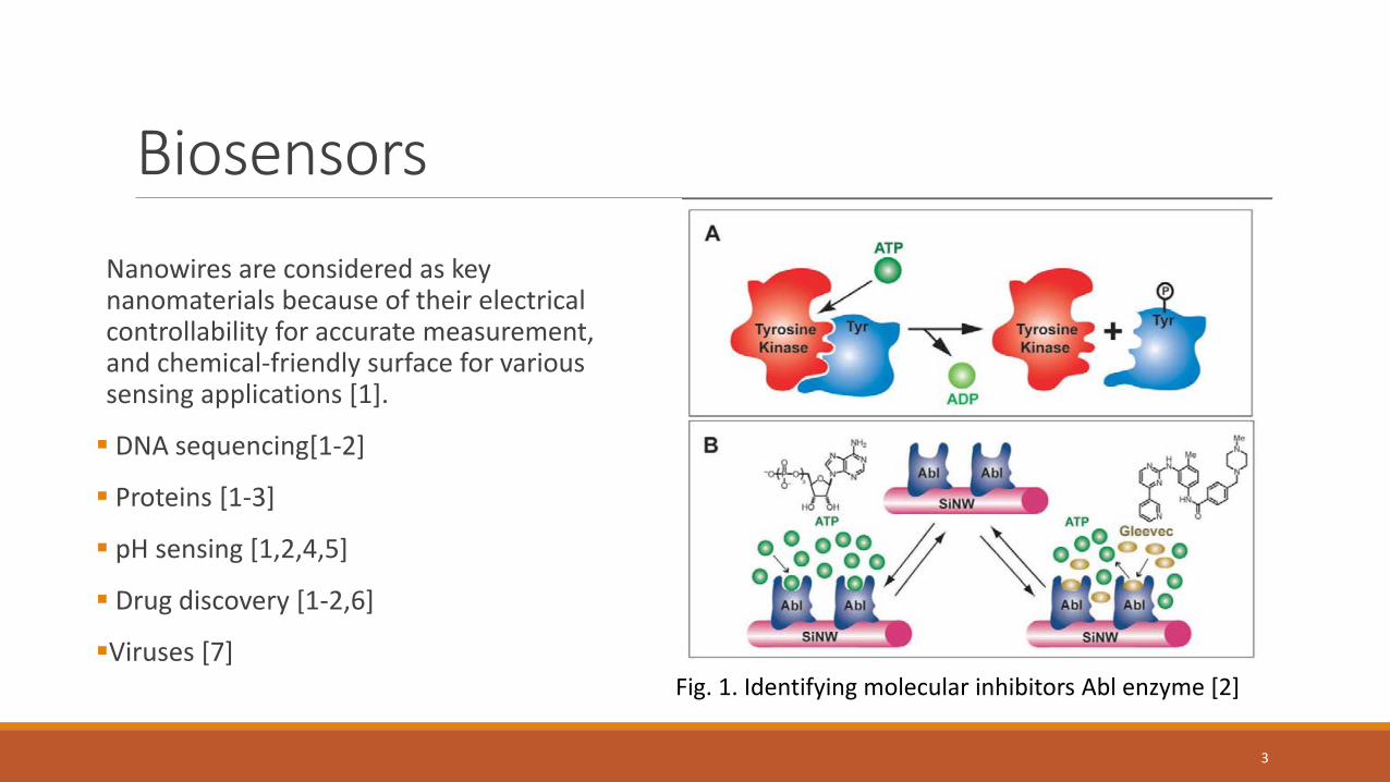
Biosensors
Nanowires are considered as key nanomaterials because of their electrical controllability for accurate measurement, and chemical-friendly surface for various sensing applications [1].
▪ DNA sequencing[1-2]
▪ Proteins [1-3]
▪ pH sensing [1,2,4,5]
▪ Drug discovery [1-2,6]
▪Viruses [7]Fig. 1. Identifying molecular inhibitors Abl enzyme [2]
3
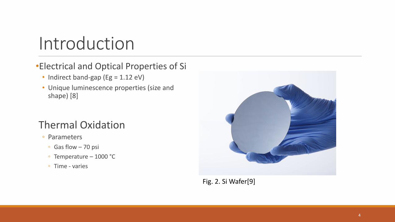
Introduction•Electrical and Optical Properties of Si• Indirect band-gap (Eg = 1.12 eV)
• Unique luminescence properties (size and shape) [8]
Thermal Oxidation◦ Parameters
◦ Gas flow – 70 psi
◦ Temperature – 1000 °C
◦ Time - varies
Fig. 2. Si Wafer[9]
4
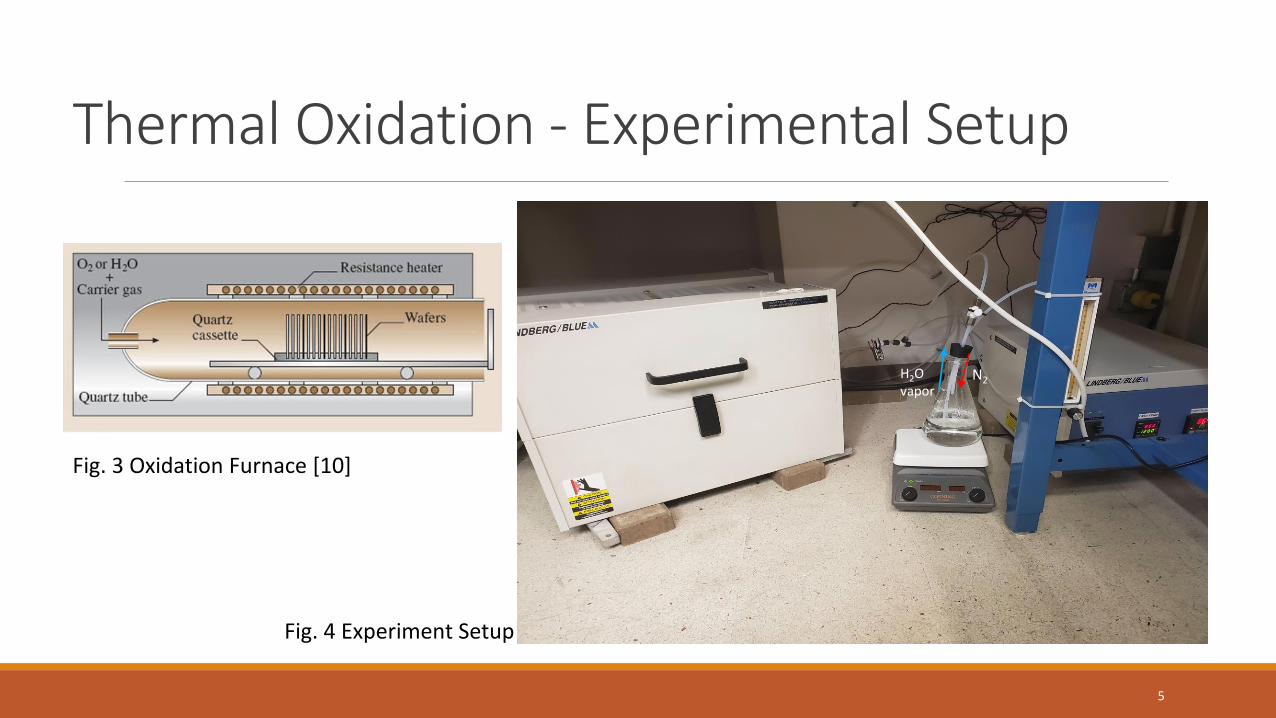
Thermal Oxidation - Experimental Setup
5
Fig. 3 Oxidation Furnace [10]
Fig. 4 Experiment Setup
N2H2O vapor

What is Wet Thermal Oxidation?
Si
Si + 2H20 SiO2 + 2H2
SiO2
Fig. 5. Explanation of thermal oxidation
6
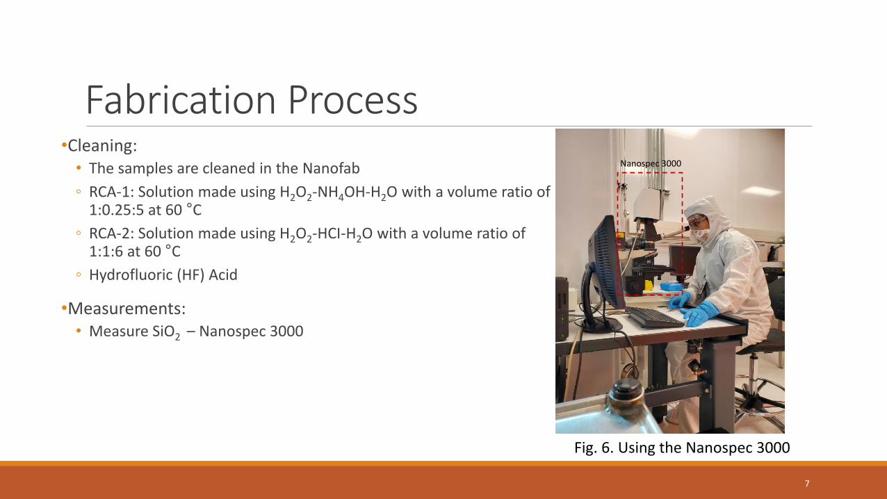
Fabrication Process•Cleaning:• The samples are cleaned in the Nanofab
◦ RCA-1: Solution made using H2O2-NH4OH-H2O with a volume ratio of 1:0.25:5 at 60 °C
◦ RCA-2: Solution made using H2O2-HCI-H2O with a volume ratio of 1:1:6 at 60 °C
◦ Hydrofluoric (HF) Acid
•Measurements:• Measure SiO2 – Nanospec 3000
7
Fig. 6. Using the Nanospec 3000
Nanospec 3000
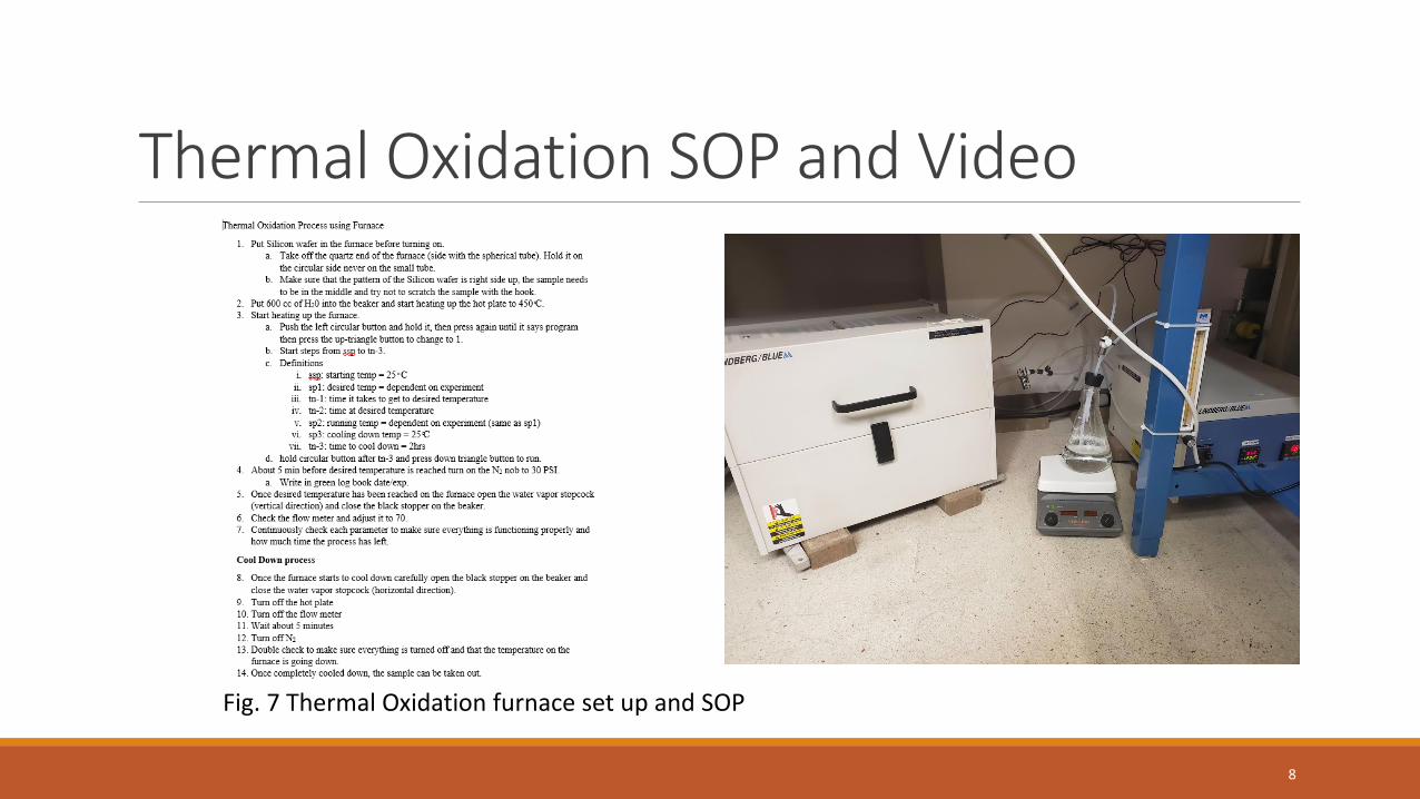
Thermal Oxidation SOP and Video
Fig. 7 Thermal Oxidation furnace set up and SOP
8

Scanning Electron Microscope (SEM)Allows for high resolution imaging at the nano and microscale [11].
Backscattered Electron Detector (BSED): Intercepts the surface and return to the surface - composition
SE – surface detail
Monte Carlo simulation◦ Interaction Volume
◦ Energy Dispersive X-Ray Spectroscopy (EDS)
Fig. 9 Monte Carlo Simulation 3 kV – 30° tilt
Fig. 8 Monte Carlo Simulation 10 kV – 0° tilt
9

Results and Discussion1. Planar
2. Trenches
3. Si Micropillars
4. Si Nanowires
10
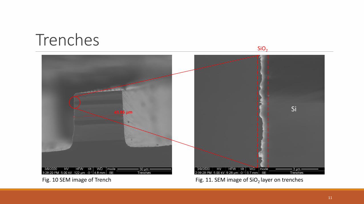
Trenches
Fig. 10 SEM image of Trench Fig. 11. SEM image of SiO2 layer on trenches
SiO2
Si
11

Fig. 12 Si Planar Sample Thermal Oxidation Graph time vs. SiO2
Growth Rate ~ 3.4049 nm/min
0
25
50
75
100
125
150
175
200
225
250
0 10 20 30 40 50 60 70 80 90 100
SiO
2th
ickn
ess
(nm
)
Time (min)
Si Planar Sample - 1000 °C
Average Thickness Average Linear (Average)
Fig. 13. Si Planar sample 1000° C (30 min)
12
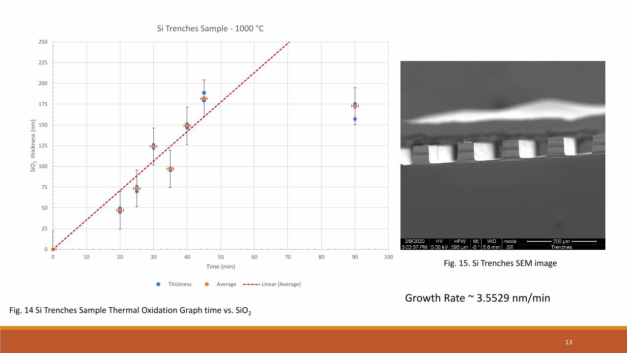
Fig. 14 Si Trenches Sample Thermal Oxidation Graph time vs. SiO2
0
25
50
75
100
125
150
175
200
225
250
0 10 20 30 40 50 60 70 80 90 100
SiO
2th
ickn
ess
(nm
)
Time (min)
Si Trenches Sample - 1000 °C
Average Thickness Average Linear (Average)
Growth Rate ~ 3.5529 nm/min
Fig. 15. Si Trenches SEM image
13

Fig. 16 Si Planar on Trenches Sample Thermal Oxidation Graph time vs. SiO2
0
25
50
75
100
125
150
175
200
225
250
0 10 20 30 40 50 60 70 80 90 100
SiO
2th
ickn
ess
(nm
)
Time (min)
Planar on Trenches Sample - 1000 °C
Average Thickness Average Linear (Average)
Growth Rate ~ 3.5346 nm/min
Fig. 17. Si Trenches sample 1000° C (30 min)
14

Fig. 18 Comparison of graphs
0
25
50
75
100
125
150
175
200
225
250
0 10 20 30 40 50 60 70 80 90 100
SiO
2th
ickn
ess
(nm
)
Time (min)
Si Trenches Sample - 1000 °C
Average Thickness Average Linear (Average)
0
25
50
75
100
125
150
175
200
225
250
0 10 20 30 40 50 60 70 80 90 100
SiO
2th
ickn
ess
(nm
)
Time (min)
Si Planar Sample - 1000 °C
Average Thickness Average Linear (Average)
Growth Rate ~ 3.4049 nm/min Growth Rate ~ 3.5529 nm/min
15
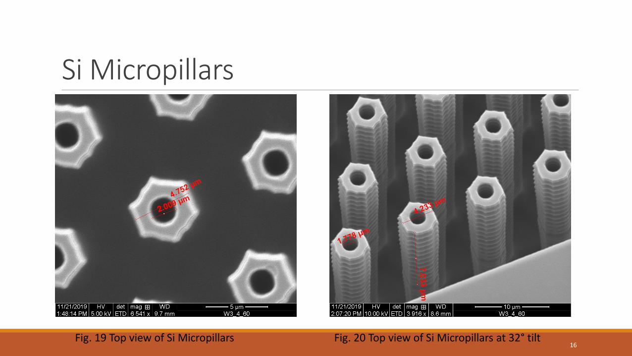
Si Micropillars
Fig. 19 Top view of Si Micropillars Fig. 20 Top view of Si Micropillars at 32° tilt16
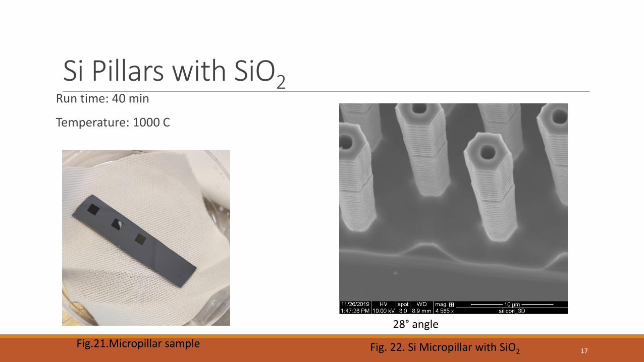
Si Pillars with SiO2Run time: 40 min
Temperature: 1000 C
28° angle
Fig.21.Micropillar sample Fig. 22. Si Micropillar with SiO2 17

Si Nanowires
Fig. 23 SEM image of Si Nanowires Fig. 24. Si Nanowires sample
18
Conclusion•Fabrication: Thermal Oxidation (shape and size)
•Characterization:• SEM and Nanospec 3000
•Growth Rate of SiO2 ~ 3.4049 nm/min
•Future Projects• Use Photoluminescence to measure optoelectrical properties
• Optimization of thermal oxidation for Si nanowires or Si micropillars
19
Resources[1] Z. Wang, S. Lee, K. Koo, and K. Kim*, “Nanowire-Based Sensors for Biological and Medical Applications,” IEEE Transactions on NanoBioscience, vol. 15, no. 3, pp. 186–199, Apr. 2016, doi: 10.1109/TNB.2016.2528258.
[2] F. Patolsky and C. M. Lieber, “Nanowire nanosensors,” Materials Today, vol. 8, no. 4, pp. 20–28, Apr. 2005, doi: 10.1016/S1369-7021(05)00791-1.
[3]Duan, X., Li, Y., Rajan, N. et al. Quantification of the affinities and kinetics of protein interactions using silicon nanowire biosensors. Nature Nanotech 7, 401–407 (2012). https://doi.org/10.1038/nnano.2012.82
[4] B. Huang, C. Hsu, Y. Wang and W. Yang, "Core-Shell P-N Junction Si Nanowires as Rapid Response and High-Sensitivity pH Sensor," in IEEE Sensors Journal, vol. 17, no. 13, pp. 3967-3974, 1 July1, 2017.
[5] Lee, J., Jang, J., Choi, B. et al. A Highly Responsive Silicon Nanowire/Amplifier MOSFET Hybrid Biosensor. Sci Rep 5, 12286 (2015). https://doi-org.ezproxy.lib.utah.edu/10.1038/srep12286
[6] M. Gu, X. Wang, T. B. Toh, and E. K.-H. Chow, “Applications of stimuli-responsive nanoscale drug delivery systems in translational research,” Drug Discovery Today, vol. 23, no. 5, pp. 1043–1052, May 2018, doi: 10.1016/j.drudis.2017.11.009.
[7] Y. Xia et al., “Label-Free Virus Capture and Release by a Microfluidic Device Integrated with Porous Silicon Nanowire Forest,” Small, vol. 13, no. 6, p. 1603135, 2017, doi: 10.1002/smll.201603135.
[8]M. Singh, M. Goyal, and K. Devlal, “Size and shape effects on the band gap of semiconductor compound nanomaterials,” Journal of Taibah University for Science, vol. 12, no. 4, pp. 470–475, 2018.
[9] Pi-Kem, Silicon Wafer. 2018.
[10]J. X. Zhang and K. Hoshino, “Fundamentals of nano/microfabrication and scale effect,” Molecular Sensors and Nanodevices Principles, Designs and Applications in Biomedical Engineering Micro and Nano Technologies, vol. 2, pp. 43–111, 2019. [E-book] Available: Elsevier
[11]Goldstein, J., Lyman, C., Newbury, D., Echlin, P., Joy, D., Lifshin, E., Michael, J. and Sawyer, L. (2003). Scanning electron microscopy and x-ray microanalysis. 3rd ed. New York [etc.]: Kluwer Academic.
20

Acknowledgements• Dr. Heayoung Yoon; Professor at the University of Utah ECE Department
• Yang Qian and David Magginetti
• Nanofab staff
• University of Utah Office of Undergraduate Research
• This work was supported by funding from Capstone Programs at the University of Utah awarded to Dinorah Segovia.
21