Design and fabrication of InN nanowire photodiode ...
7
1 13 December 2013 DRDC-RDDC-2013-L6 Produced for: LCol Luc Angiolini, CANSOFCOM COS FD Scientific Letter Design and fabrication of InN nanowire photodiode detectors for SWIR Background This scientific letter gives the status regarding the project 06cd19 to support CANSOFCOM. Cameras have, at their heart, photo detectors. The latter are made of materials that are sensitive to a specific wavelength band, such as visible, UV, short wave infrared (SWIR), etc. The efficiency of detecting incoming photons and convert them into information to perform imagery is a constant challenge and command to search for new materials to be used as detectors. Among these, InN nanowires were presented by McGill University as promising because InN can respond to a much wider wavelength range than conventional material such as InGaAs. Moreover, InN nanowires are grown directly on Si substrates and can be readily integrated with Si electronics on the same chip, which would reduce the integration cost by a factor of three to five. To investigate the feasibility to use InN nanowires for SWIR detection, a contract (W7701-135487) was granted to McGill University on 20 December 2012. The tasks comprised the design and the fabrication of a single detector using InN nanowires tuned for the absorption in the spectral range of 0.9 μm – 2.0 μm broadband which corresponds to the SWIR band. The single detector would be characterized to evaluate if the performance is better than conventional InGaAs detectors. The contract stipulated that after 12 months, a go-no-go decision would be taken on whether or not to grant an additional year of research to the contract. The decision would be based on the short term (12 months) realistic potential of the nanowires to perform better than the typical material used for SWIR detection, the InGaS thin film. On 20 November 2013, the decision was announced to McGill University that the optional year would not be granted. This letter gives the rational for the decision. The section Statement of Results summarizes the results obtained by McGill University. Interpretation of the results, our understanding and details of our rational for the decision are explained in the Discussion of Results section.
Transcript of Design and fabrication of InN nanowire photodiode ...
1
13 December 2013
DRDC-RDDC-2013-L6
Produced for: LCol Luc Angiolini, CANSOFCOM COS FD
Scientific Letter
Design and fabrication of InN nanowire photodiode detectors for SWIR Background This scientific letter gives the status regarding the project 06cd19 to support CANSOFCOM.
Cameras have, at their heart, photo detectors. The latter are made of materials that are sensitive to a specific wavelength band, such as visible, UV, short wave infrared (SWIR), etc. The efficiency of detecting incoming photons and convert them into information to perform imagery is a constant challenge and command to search for new materials to be used as detectors. Among these, InN nanowires were presented by McGill University as promising because InN can respond to a much wider wavelength range than conventional material such as InGaAs. Moreover, InN nanowires are grown directly on Si substrates and can be readily integrated with Si electronics on the same chip, which would reduce the integration cost by a factor of three to five.
To investigate the feasibility to use InN nanowires for SWIR detection, a contract (W7701-135487) was granted to McGill University on 20 December 2012.
The tasks comprised the design and the fabrication of a single detector using InN nanowires tuned for the absorption in the spectral range of 0.9 μm – 2.0 μm broadband which corresponds to the SWIR band. The single detector would be characterized to evaluate if the performance is better than conventional InGaAs detectors.
The contract stipulated that after 12 months, a go-no-go decision would be taken on whether or not to grant an additional year of research to the contract. The decision would be based on the short term (12 months) realistic potential of the nanowires to perform better than the typical material used for SWIR detection, the InGaS thin film.
On 20 November 2013, the decision was announced to McGill University that the optional year would not be granted.
This letter gives the rational for the decision.
The section Statement of Results summarizes the results obtained by McGill University. Interpretation of the results, our understanding and details of our rational for the decision are explained in the Discussion of Results section.

2
Statement of Results Using the molecular beam epitaxial (Figure 1), Prof Mi and his team succeeded to grow InN nanowires on Silicon wafers.
Figure 1: Molecular beam epitaxial (MBE) used to grow InN nanowires.
They investigated two designs for the photodiode: P-I-N (Positive-Intrinsic-Negative) photodiode (Figure 2a) and I-P (Intrinsic-Positive) (Figure 2b).
(Recall that doping intentionally introduces trace impurities (atoms) into an extremely pure (referred to intrinsic) semiconductor for the purpose of altering its electrical properties. The positive region is doped with atoms that increase significantly the number of electron vacancies (holes) and the negative region is a region doped to increase the concentration of electrons than holes.)
Figure 2:Photodiode design investigated: a) PIN, b) IP.
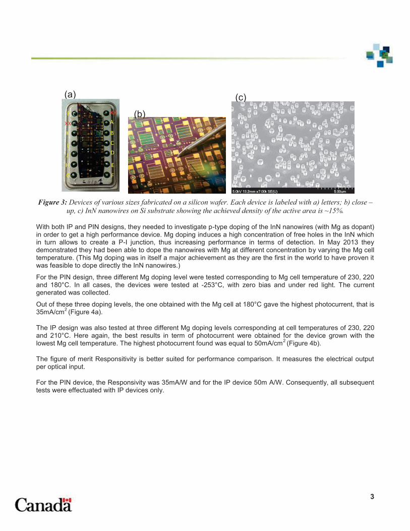
They built devices of various sizes from 1mm by 1mm to 300mm by 300mm (Figure 3). The achieved fill factor (density of nanowires in the active area) was calculated to be roughly 15%.
(a) (b)
3
Figure 3: Devices of various sizes fabricated on a silicon wafer. Each device is labeled with a) letters; b) close –
up, c) InN nanowires on Si substrate showing the achieved density of the active area is ~15%.
With both IP and PIN designs, they needed to investigate p-type doping of the InN nanowires (with Mg as dopant) in order to get a high performance device. Mg doping induces a high concentration of free holes in the InN which in turn allows to create a P-I junction, thus increasing performance in terms of detection. In May 2013 they demonstrated they had been able to dope the nanowires with Mg at different concentration by varying the Mg cell temperature. (This Mg doping was in itself a major achievement as they are the first in the world to have proven it was feasible to dope directly the InN nanowires.)
For the PIN design, three different Mg doping level were tested corresponding to Mg cell temperature of 230, 220 and 180°C. In all cases, the devices were tested at -253°C, with zero bias and under red light. The current generated was collected.
Out of these three doping levels, the one obtained with the Mg cell at 180°C gave the highest photocurrent, that is 35mA/cm2 (Figure 4a).
The IP design was also tested at three different Mg doping levels corresponding at cell temperatures of 230, 220 and 210°C. Here again, the best results in term of photocurrent were obtained for the device grown with the lowest Mg cell temperature. The highest photocurrent found was equal to 50mA/cm2 (Figure 4b).
The figure of merit Responsitivity is better suited for performance comparison. It measures the electrical output per optical input.
For the PIN device, the Responsivity was 35mA/W and for the IP device 50m A/W. Consequently, all subsequent tests were effectuated with IP devices only.
(a)
(b)
(c)

4
Figure 4: Best photocurrent response results obtained under red light at -253°C and zero bias with a) the PIN
design and b) the IP design.
In order to increase the generated photocurrent, the next experiments were conducted with negative bias down to -1.3V. To comply with the contract requirements the tests were done in the SWIR band (900-1500nm) and at room temperature (300 K).
Figure 5 illustrates respectively Photocurrent, Responsivity and D* obtained for the IP device in those testing conditions.
(a) (b)

5
Figure 5: a) Photocurrent response of IP device (only 1550nm is shown). In the inset, the dark current is reported; b) responsivity showing a max value of 0.2 A/W,) specific detectivity D* curve showing a maximum
value of 107 to 108 Jones.
(c)(b)
(a)

6
Discussion of Results
When negative bias was applied to the IP device, Figure 5b shows that the responsivity jumped three orders of magnitude going from 50mA/W under red light to 02 A/W under SWIR. That was good news.
However, it is the specific detectivity D* (equation 1) that is the most important figure of merit.
(1)
This figure of merit represents the ratio of the responsitivity (R) time the photosensitive region of the detector (A), over the noise spectral density (Sn).
The noise spectral density is greatly determined by the dark current which is an intrinsic electric current always present in a diode, even when no photons are entering the device. Low temperature minimizes this noise but cooling the detector is not an option for the application foreseen with this material.
As seen in the inset of Figure (5a), the dark current rises when a bias is applied. Therefore, the apparent gain in photocurrent is unfortunately counterbalanced by a rise of noise. The net effect is a D* that is not very good.
In Figure (5c), the D* of the IP prototype is 107 to 108 Jones, which is five orders of magnitude less than the typical D* value found for InGaAs thin film (1013 Jones). This gap is significant.
To explain this low D* value, McGill University pointed out many aspects of their fabrication process they intended to improve in the second year of the contract.
They first mention that the actual fill factor was only 15% and they are confident to increase it to 80% (the typical value for InGaAs thin film) by optimization of the seeding layer. They claim this achievement could be done easily within 12 months. We also agree with their affirmation.
McGill University added that the quantity of absorbed photons would increase (by less than an order of magnitude) with an ITO layer (antireflection material). Preliminary data not shown here, obtained with coated devices confirmed that.
Yet, absorbing more photons is desirable but the device must convert the photons in electrical current. This efficiency of conversion is critical. With their actual device, they calculated that the IQE (Internal quantum efficiency) to be somewhere in the range of 8 to 22%. With an ITO layer and a fill factor superior to 60%, they claim to be able to raise the IQE to 80% in one year. We are not as optimistic as them on this. Moreover, the responsivity curve in Figure 4b shows an important drop beyond 1080nm. Responsivity at 1500nm is half that of 1080nm. Knowing that 1500nm is the wavelength of interest in the SWIR band, this is not good news.
McGill University correctly recognised leakage current in the IP device, as a limiting factor for the improvement of the responsivity. They identified potential trouble sources in their fabrication process such as presence of over-etching and passivation surface problems. Optimizing micro-fabrication processes takes time and this challenge of getting rid of the leakage current is not to be minimized in our opinion.

7
But in the end, these above enhancements would improve performance of the nominator numbers in the D* equation. But at the denominator, the dark noise is still very high. It is the dark current McGill University has to decrease drastically to reach equivalent or better performance than the InGaAs film.
To address this problem, McGill University proposes to reduce the dark current using a core-shell structure they have developed for another project involving InN nanowires. The core-shell structure implies that another material, InGaN, is deposited around the InN nanowire in such a way that it forms a shell around it. This shell acts as a carrier confinement for the high density of electrons at the near-surface region of the nanowire. The shell thus greatly reduces generation of electrons and holes at this surface. That would reduce the dark current.
They estimated they could increase the D* to 108 to 109 Jones in 12 months with this core-shell strategy. Recall that typical InGaAs has D* of 1013 Jones. They further propose to cool down the detector with thermoelectric cooling to get 1013 Jones. Again, note that those actual SWIR detectors are not cooled.
Conclusion
The military mandate for this project was clear: to give the status on the maturity of this emerging technology for SWIR detection and grant funding for a second year if performance were expected to exceed those of InGaAs film within a year.
Considering all the above, we have acknowledged the great work McGill University has done throughout this project but we believe that exceeding performance of typical InGaAs film is not achievable in twelve months. Therefore, the optional year was not granted.
This objective of the project has been met.
Prepared by: Suzanne Paradis
Revised by: Philippe Mérel
This Scientific Letter is a publication of Defence Research and Development Canada. The reported results, their interpretation, and any opinions expressed therein, remain those of the authors and do not necessarily represent, or otherwise reflect, and official opinion of the Canadian Armed Forces (CAF), Department of National Defence (DND), or the Government of Canada.
© Her Majesty in Right of Canada (Department of National Defence), 2013.