Design and Fabrication of Antireflection ZnO Thin Film by ...
101
Republic of Iraq Ministry of Higher Education and Scientific Research AL-Nahrain University College of Science Department of physics Design and Fabrication of Antireflection ZnO Thin Film by Using Different Techniques A Thesis Submitted to the College of Science, Al-Nahrain University in Partial Fulfillment of the Requirements for Degree of Master of Science in Physics. By Nidaa Taha Yaseen B.Sc., Mustansiriya University (2005) Supervised by Dr. Alaa J. Ghazai (Assistant prof) July 2017 shawal 1438
Transcript of Design and Fabrication of Antireflection ZnO Thin Film by ...

Republic of Iraq
Ministry of Higher Education
and Scientific Research
AL-Nahrain University
College of Science
Department of physics
Design and Fabrication of
Antireflection ZnO Thin Film by
Using Different Techniques A Thesis
Submitted to the College of Science, Al-Nahrain University in Partial
Fulfillment of the Requirements for Degree of Master of Science in
Physics.
By
Nidaa Taha Yaseen
B.Sc., Mustansiriya University (2005)
Supervised by
Dr. Alaa J. Ghazai
(Assistant prof)
July 2017 shawal 1438

صدق الله العلي العظيم
1الآية سورة الفتح


DEDICATION
TO
MY, FATHER AND MOTHER SOIL
(ALLAH MERCY), DAUGHTER
SHAMS, BROTHERS, AND
FAMILY

ACKNOWLEDGEMENTS
First and foremost, I would like to thank Allah for granting me
good health and patience to complete this research. I would also like to
express sincere gratitude to my supervisor Asst.prof. Dr. Alaa Jabbar,
Ghazai for his intellectual guidance; devoted time and support for
completing this work. I would like to send my thanks to my fiance
Mohamed Fouad for valuable guidance, comments and support
throughout this thesis. I appreciate the help of Dr.Wisam, J. Aziz for
valuable suggestions, and I extend my thanks and gratitude to Dr.
Hassan to help me in this research, I also express my gratitude to my
friends especially in Physics Department, Science College, Al
Nahrain University whom help and guided me at all time during my
study. I would also like to thank the Lab staff of Physics
Department, Science College, Al Nahrain University and
Mustansiriya University, to allow me to used the Lab freely and
made all my Preparations and determinations and for the attention
and assistance they have given me through years.
I would like to express my gratitude to my dear brother Laith Taha
Yaseen for giving me great love, endless support, sympathy and
encouragement when I needed it.
Lastly, big thanks to my lovely country Iraq, and Al Nahrain
University, especially, the lectures and staff in Physics Department
and Science College.
I
List of Contents
Contents
List of Contents I
List of Table II
List of Figures II
List of Symbols V
List of Abbreviations VI
Summary VII-VIII
Chapter one: Introduction and Literature Review
1.1.Intruduction 1
1.2.Anti-Reflaction coating (ARCS) 1
1.3.Tin-Film Interference 2
1.4.Type of Interference Coating (ARCS) 4
1.5.ZnO Structure 7
1.6.Method of Thin Film Growth Technique 8
1.9.Literayure Review 9
1.10.Aim of the Work 14
1.11.Outline of Work 14
Chapter Two: Theoretical Part
2.1.Introduction 15
2.2.The Characteristic Matrix of Single Thin Film 15
2.3.Pulse laser ablation 18
2.4.Laser Beam Parameters 20
2.5.Spin Coating Parameters 22
2.6.Structure Parameters Analyses 23
2.10.Optical Properties 26
Chapter Three: Experimental Part
3.1.Introduction 31
3.2.Substrate parameter and Cleaning 32
3.3. ZN Target and Colloidal Solution 33
3.4.Laser Ablation System 34
3.5.Preperation ZnO thin film using sol gel method 35
3.6.The Characterization Instruments 36
3.7. Thickness Measurement 37
Chapter Four: Result and Discussion
4.1.Intruduction 38
4.2.Single Layer 38
4.3.Structure Result of ZO ARCS 40

II
4.4.Scanning Electron Microscopes (SEM) Results 48
4.5.Optical Properties 59
4.6 Optical Properties Results of ZO Nanoparticle by Sol-Gel
Technique
66
Chapter Five Conclusion and Future Works
5.1.Conclusion 68
5.2.Future Works 68
References
List of Tables
Figure
No.
Caption Page
No.
(1-1) properties of bulk wurtzite lattice structure of
ZnO
8
(4-1) Theoretical reflection values of uncoated and
coated with ZnO film substrates
39
(4-2) The result of the XDR for ZnO nanoparticles at
different
47
(4-3) Experimental result for different pulse laser
number
62
(4-4) Experimental result for different laser energy 64
(4-5) Experimental result 2000 pulse of different
solvent
66
List of Figures
Figure
No.
Caption Page
No.
1.1 The thin film interference at interfaces of film with
geometric thickness (d)
3
1.2 The system of antireflection layer (ARCS) of a-Single
layer b- Double layer c-Multi layer
4
1.3 The types of ARCS according to its optical performance 6
1.4 The wurtzite lattice of ZnO: small circles represent zinc
atoms, whereas large circles depict oxygen atoms
7
1.5 planned of thin film deposition techniques 9

III
2.1 Plane wave falling on the thin film 15
2.2 Laser ablation in Solution technique 19
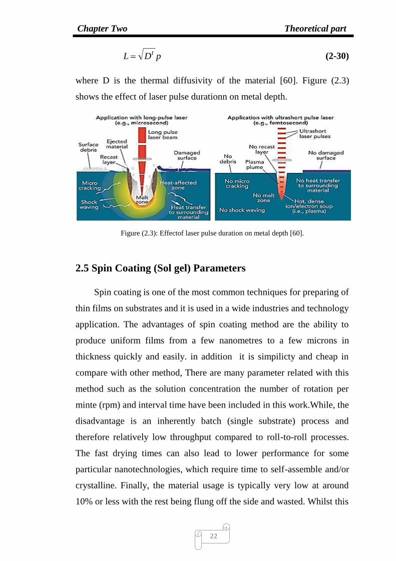
2.3 Effect of laser pulse duration on metal depth 22
2.4 FWHM of The Preferred Orientation of the X-Ray
Diffraction Pattern
24
2.5 an Edge Dislocation in a Simple Cubic Lattice 25
2.6 The Formation of Energy Bands in Silicon Lattice Crystal
By Bringing Together Isolated Atoms
27
2.7 Fundamental Absorption Edge of Crystal Semiconductor 28
2.8 the optical transitions (a) Allowed direct, (b) Forbidden
direct; (c) Allowed indirect, (d) Forbidden indirect
30
3.1 The Diagram of experiment steps of research under
studying
31
3.2 (a) Schematic of porous silicon set-up (b) the
electrochemical etching cell.
33
3.3 Experimental setup for nanoparticles synthesis by PLA
process
34
4.1 transmission curve as a function of wavelength of ZnO
thin film on glass substrate
40
4.2 The XRD pattern of ZnO nanoparticle on glass substrate
with laser pulses number of 1000, 1500, and 2000 pulse at
energy 700 mJ a- methanol solvent b- distilled water
solvent
42
4.3 The XRD pattern of ZnO nanoparticle on glass substrate
with laser pulses number of 1500 pulse at energy 600 mJ
,700 mJ and 800mJ
43
4.4 The XRD pattern of ZnO nanoparticle on glass substrate
with laser pulses number of 1500 pulse at energy 700 mJ
in distilled water and methanol solvents.
44
4.5 The XRD pattern of ZnO nanoparticle on glass and Si
substrates prepared using PLA method with laser pulses
number of 1500 pulse at energy 700 mJ dissolved in
distilled water solution
45
4.6 The XRD pattern of ZnO nanoparticle on glass and PSi
substrates prepared using sol gel method
46
4.7 SEM images of ZnO thin film on glass substrate prepared 49

IV
using PLA method in methanol solvent with energy 700
mj and pulses of a- 1000, b-1500, and c-2000 pulses
4.8 SEM cross section of ZnO thin film 50
4.9 EDX analysis of ZnO thin films prepared by PLA method
on glass substrate with energy 700 mj at pulses a-1000, b-
1500 and c-2000 pulses in methanol solvent
51
4.10 SEM images of ZnO thin film on glass substrate prepared
using PLA in distilled water solvent with energy of 700 mJ
and pulse of a-1000, b-1500, and c-2000
52
4.11 EDX analysis of ZnO thin films prepared by PLA method
on glass substrate with energy of 700 mj and at pulse
number a-1000, b-1500, and c-2000 pulses in distill water
solvent
53
4.12 SEM images of ZnO thin film on glass substrate prepared
using PLA at pulse number of 1500 and with energy of a-
600, b-700 and c-800 mJ
55
4.13 EDX analysis of ZnO thin films prepared by PLA method
on glass substrate with energy of a-600 ,b-700, and c-800
mj in methanol solvent
56
4.14 SEM images of ZnO thin film on Psi substrate prepared
using PLA with pulse 2000 and energy 700 mJ
57
4.15 EDX analysis of ZnO thin films prepared by PLA method
of PSi substrate in methanol solvent.
57
4.16 SEM images of ZnO thin film on a-glass substrate b-p si
sub prepared with sol-gel method with (3000) rotation
throw 10 minute.
58
4.17 EDX image of ZnO thin films a-Glass substrate b- pSi
substrate prepared using spin coating method
59
4.18 Transmittance spectra as function of wavelength of ZnO
thin films at different Pulses number of 1000, 1500 and
2000 dissolved in a- methanol solvent and b- distill
water solvent
60
4.19 A Plots of (αhν)2 verses photon energy (hν) of doped ZnO
thin films at different of pulses number a- methanol
solvent b- distilled water solvent
61
4.20 Transmittance spectra of ZnO thin films at different laser
energy with 600,700 and 800 mJ of methanol solvent.
63

V
4.21 A Plots of (αhν)2 verses photon energy (hν) of doped ZnO
thin films at different laser energy
64
4.22 Transmittance spectra of ZnO thin films at different
solvent type (methanol and distill water) solvent
respectively.
65
4.23 A plots of (αhν)2 verses photon energy (hν) of doped ZnO
thin films of different solvent type
66
4.24 Transmittance spectra of ZnO thin films in case of coated
and uncoated the substrate.
67
4.25 A plots of (αhν)2 verses photon energy (hν) of doped ZnO
thin films in sol gel method
67
List of Symbols
Symbols Description Units
A Absorption -
ARCs Antireflection coating system -
E Electric field vector N/Colum
H Magnetic field vector Tesla
J Current density Amp/m2
K Wave vector 1/nm
N Imaginary part of refractive index -
n Real part of refractive index -
σ Conductivity Siemens/m
R Reflection Siemens/m
r* Reflection coefficient -
S Panting vector -
T Transmission -
ω Angler momentum nt.m.s
ε Dielectric constant (Permeability) Fm-1
μ Permittivity Mm-1
α Absorption coefficient cm-1
λ Wavelength nm or A0
λd Design wavelength nm or A0
FE Field emission
Eg Energy gap eV
VI
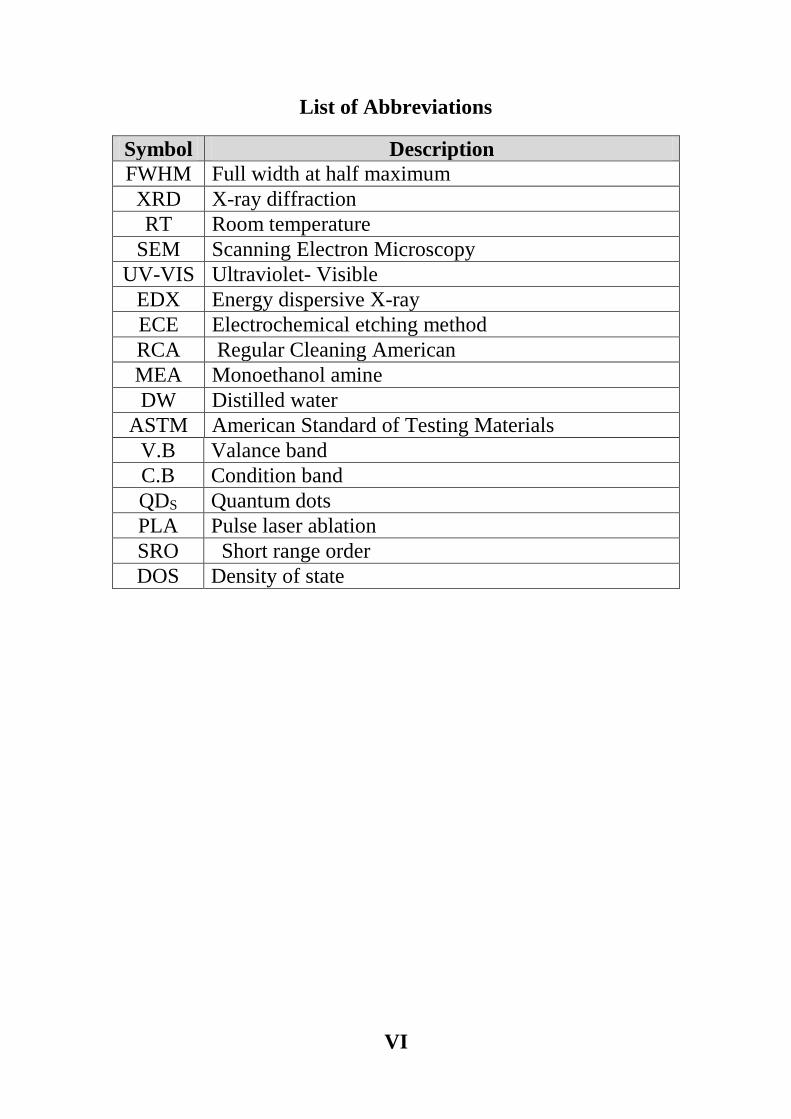
List of Abbreviations
Symbol Description
FWHM Full width at half maximum
XRD X-ray diffraction
RT Room temperature
SEM Scanning Electron Microscopy
UV-VIS Ultraviolet- Visible
EDX Energy dispersive X-ray
ECE Electrochemical etching method
RCA Regular Cleaning American
MEA Monoethanol amine
DW Distilled water
ASTM American Standard of Testing Materials
V.B Valance band
C.B Condition band
QDS Quantum dots
PLA Pulse laser ablation
SRO Short range order
DOS Density of state

VII
Summary
In this work single layer antireflection coating of ZnO thin film has
been designed and fabrication on glass and PSi substrates using pulse
laser ablation (PLA) and spin coating techniques.
Mainly, the work, divided into two parts, first: single antireflection
of ZnO thin film using modified characteristics matrix to satisfy zero
reflection condition theoretically. Second: ZnO nanoparticle deposited on
different substrates using PLA which including the effect of duration
pulse of 1000, 1500, 2000 pulses, Energy of 600, 700, 800 mJ and type of
solvent by methanol and distilled water have been fabricated studied. In
addition, spin coating method have been employed to synthesis this film.
Structural and optical properties of prepared films have been
characterized using XRD, SEM and EDX, and UV-Vis, respectively.
XRD results revealed that the ZnO thin film have hexagonal structure
with polycrystalline in nature with preferred orientation of (002). In
addition, crystalline size was increased with the increasing of duration
pulses at methanol solvent at fixed energy of 700 mJ, besides; in distilled
water solvent at 700 mJ have low crystalline size at duration pulse of
1500 pulse. While at fixed duration of 1500 pulse, the crystalline size has
low valne at energy of 700 mJ . As well as, the film deposited on glass
and PSi substrate using sol gel method have crystalline size of (96.83and
85.16) nm respectively.
Narrow FWHM and no phase change has been observed in all cases.
SEM images showed that for all cases the films were homogenous with
some island and cluster then cracking started to obtain with the increasing
of increase the pulse number. Expected of film on glass prepared using
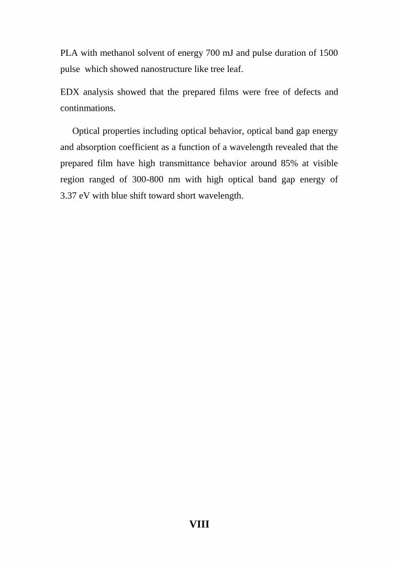
VIII
PLA with methanol solvent of energy 700 mJ and pulse duration of 1500
pulse which showed nanostructure like tree leaf.
EDX analysis showed that the prepared films were free of defects and
continmations.
Optical properties including optical behavior, optical band gap energy
and absorption coefficient as a function of a wavelength revealed that the
prepared film have high transmittance behavior around 85% at visible
region ranged of 300-800 nm with high optical band gap energy of
3.37 eV with blue shift toward short wavelength.

Chapter One
Introduction

Chapter One Introduction and Literature Review
1
1.1 Introduction
In order to make size and structure dependent properties and
phenomena, as distinct from those associated with individual atoms or
molecules with bulk materials to manipulate and control matter in
nanoscale, the nanotechnology have been applied. The term “nanoscale”
is called on the structure size ranged from 1 to 100 nanometers (nm),
which have great scientific interest as they are effectively a bridge
between bulk materials and atomic or molecular structures. In this size,
physical, chemical, and biological properties of substances are different
from that of the micrometer and larger scales and these new properties of
the materials, devices and systems could be develop unlimited [1,2].
There are two reasons for these unique properties could listed as
following:
1- At the scale of nanometers, particles and structures have a very high
surface-to-mass ratio. Makes them highly reactive compared to their
bulk structure.
2- Nanometers exist in the term of quantum physics, and quantum
properties are similarly valuable in developing enhanced materials [3].
In last a few years, zinc oxide (ZnO) nanostructure thin film have
been attracted more attention due to the unusual properties of high
transparency in the visible spectrum In addition , high chemical stability,
excellent electrical and optical properties; with a wide band gap energy
of 3.37 eV, which make it more suitable for short-wavelength
optoelectronic applications [4,5]. Besides, ZnO has a large exciting
binding energy of 60 mv at room temperature.
1.2 Antireflection Coating (ARC)
An anti-reflection coating (ARC) is widely used in most of
the optical applications to reduce the unwanted reflection on the

Chapter One Introduction and Literature Review
2
surfaces of the optical components [6] which improves the
efficiency by reduce the light lost, it's consiste of a thin layer or
multilayer, which may be isolating dielectric materials[7], metals, or a
mixture of isolating materials.[8,9]. The main property of isolating
films it's have low absorption (α < 103 cm-1) [7]
Anti-reflective coatings are used in a wide variety of
applications such as anti-glare coatings on corrective lenses, camera
lens elements, solar cells[7], arial survy camera, star sensors, and
thermal imaging system[10].
The anti-reflection phenomenon has been define firstly by
Rayleigh as results from the surfaces of optical components that are
coated with a particular substance (using chemical methods)[11].
Early references to the science of thin film deposition
include the research conducted by Michael Faraday in 1857.
Faraday created thin metallic films which thermally induced evaporation
using electrical heat resistance by allowed an electric current to pass
through a metallic wire and heat it to would evaporate[12].
1.3 Thin-Film Interference
Mathematical analysis of light interference at and through thin-
film boundaries carry out using the relations that described the spread
of the optical wave inside each layer on the interface that separate the
layers . let's consider a light beam coming from a light source (S)
fall on a thin film with a geometric thickness of d at a point ( A ).
Nnaturally, part of the light will be reflected back to the same
incident medium in the direction of the (1) ray and some will be
transmitted towards (AF), and when it arrives to point F, part of
this ray will reflect also to point B and another part will be
transmit towards H. as well as, at point B, the ray (FB) will continue
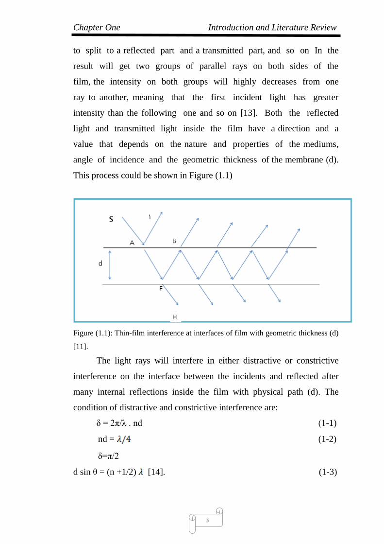
Chapter One Introduction and Literature Review
3
to split to a reflected part and a transmitted part, and so on In the
result will get two groups of parallel rays on both sides of the
film, the intensity on both groups will highly decreases from one
ray to another, meaning that the first incident light has greater
intensity than the following one and so on [13]. Both the reflected
light and transmitted light inside the film have a direction and a
value that depends on the nature and properties of the mediums,
angle of incidence and the geometric thickness of the membrane (d).
This process could be shown in Figure (1.1)
Figure (1.1): Thin-film interference at interfaces of film with geometric thickness (d)
[11].
The light rays will interfere in either distractive or constrictive
interference on the interface between the incidents and reflected after
many internal reflections inside the film with physical path (d). The
condition of distractive and constrictive interference are:
δ = 2π/λ . nd (1-1)
nd = (1-2)
δ=π/2
d sin θ = (n +1/2) [14]. (1-3)

Chapter One Introduction and Literature Review
4
where n represents of Refractive index , δ represents the Angle phase
difference.
The speed of propagation of electromagnetic wave in material
mediums is determined by nodular refraction coefficient (N) [14] :
N = n – ik (1-4)
where n represents the real part of refractive index N
k represents the extinction coefficient which is the imaginary part
of N , and is connected to absorption coefficient (α) by the relation :
α = 4πk / λ (1-5)
where λ is the wavelength of the incident light
1.4 Types of Antireflective Coatings (ARCs)
The main principle of the thin-film optical coating's is based
on the constructive and destructive interference principle between
the light rays emerging from thin-film coating after suffering
multiple internal reflections in the interfaces of these layers [7].
ARCs classified into several types according to:
Firstly, Number of Layer used into:
a- Single layer, b- Double layer, c- Multilayer
As shown in Figure (1-2)
III
Figure (1.2) the system of antireflection layer (ARCS) of a- Single layer b- Double layer c-
Multi layer [8].
2n
mn
s Substrate n
snSubstrate
Substrate ns ns
1,d1n 1,d1n
1n
2,d2n
OI
O
R
on R
c
OI
O
R
OI
O
R
b a

Chapter One Introduction and Literature Review
5
where …n1 ,n2 …,d1 , d2 … refractive indices and geometric
thicknesses of layers, respectively.
Secondly, Optical performance : which As the reflectance or
transmittance or absorbance is a function of the wavelength or
frequency so it is defined according to the following optical per
formant:
a- V-type : Where the reflectance equal zero at the design
wavelength λo [15].
b- W-type : This type is characterized by the presence of
two regions of the spectrum where the reflectance equal
zero , and in the middle a narrow area where the
reflectivity is equal to the reflectivity of the substrate
[15,16].
c- U-type: Where the reflectivity equals zero at a specific range
of wavelengths [10].
d- Extended U-type : Where the reflectivity equals zero at a
wide range of wavelengths [10].
e- π-type : This type is designed to operate at two specific
wavelengths at the same time , where reflectivity equals
zero at these two wavelengths and is high at other
wavelengths[17].
Each one of these types has it's specific use for instance :
V-type is used in LASER systems specifically at the
Nd:YAG wavelength, [18] while W-type is used in the same
LASER systems but at two wavelengths that are very close
to each other . These types of ARCS according to its optical
performance is show in Figure (1.3).

Chapter One Introduction and Literature Review
6
Figure (1.3)
Types of ARCS according to its optical performance [18].
Thirdly: Substrates refractive index which is divided in to: a-Low-
refractive index substrate; In this type the coating is precipitated
on a substrate of low refractive index which used to study the
spectrum distribution in the visible region and the near-infrared
region, such as BK-7 glass [(ns = 1.52) at a design wavelength (λ0 =550
nm)] [11].
b-High – refractive index substrate; In this type the coating is
precipitated on a substrate of high refractive index which used
to study the spectrum distribution in the infrared region of the
electromagnetic spectrum , such as Germanium (Ge) [(ns = 4.0) at
design wavelength (λ0 = 2.3 µm)] and Silicon (Si) [(ns = 3.42) at
design wavelength (λ0 =1.7 µm)] [19].
λ
oλ
W_ Type
λ
R
λ
R
λ
R
λ
oλ
V_ Type
π-Type Extended U-Type U-Type

Chapter One Introduction and Literature Review
7
1.5 ZnO Structure
Zinc oxide (ZnO) is a wide-bandgap semiconductor of the II-VI
semiconductor group. polar hexagonal structure; the c axis is parallel
to z axis and has prefer orientation of (0002). In almost
ZnO, zinc atoms arrangement in hexagonal close packing (hcp). While,
the oxygen atom have tetrahedral structure surrounding by four zinc
atoms as shown in Figure 1.4.The two lattice parameters, a and c of
hexagonal unit cell in wurtzite structure with ratio of
c/a=1.633 and belongs to the space group of P63mc - C46ν
are= (0.3296 and c = 0.52065 nm) [20].
Figure (1.4): The wurtzite lattice of ZnO: small circles represent zinc atoms, whereas
large circles depict oxygen atoms [20].

Chapter One Introduction and Literature Review
8
Table (1.1): shown the properties of bulk wurtzite lattice structure of
ZnO [20].
Value Property
a= b=3.25 A
c= 5.21 A
u= 0.348
c/a= 1.593-1.6035
Lattice parameter
5.606 gm/cm3 Density
2248 K Melting point
Wurtzite Stable crystal structure
8.66 Dielectric constant
2.008 Refractive index
3.37 eV,(direct) Band gap (Eg)
60 me V Exciton binding energy
0.24 /0.59 Electron/ Hole effective mass
5-50 cm3/Vs Hole mobility (300) K
100-200 cm2/ Vs Electron mobility (300) K
1.6 Method of Thin Film Growth Technique
There are different methods to growth the thin film, in present
work ZnO films have been prepared using chemical process spin coating
(sol gel) and physical process pulse laser ablation (PLA) techniques [21].
These techniques are planned in Figure (1.5) as method of thin film
deposition.

Chapter One Introduction and Literature Review
9
Figure (1.5): planned of thin film deposition techniques [21].
1.7 Literature Review
There are many studied in regard with design and fabrication of
ZnO thin film. The reviews the ZnO materials properties and the relevant
research's on the structural and optical properties of ZnO films and its
associated preparation techniques have been reported.
Two techniques were used throughout the study to fabricate ZnO thin
films. The techniques include the PLA, and sol-gel.as fallows:

Chapter One Introduction and Literature Review
10
Firstly, review on prepared ZnO thin film using PLA techniques
are studied, In 2001, Singh et al. prepared highly conductive and
transparent Al-doped zinc oxide (ZnO:Al) thin films by (PLA) technique
with irradiation time of 10-60 min (6000-36000 laser shots)[22]. Then,
in 2006, Ishikawa, et al. successfully, produced zinc oxide nanorods
using (PLA) in deionized water media at high temperature and at room
temperature[23]. In addition, Chen and Zhang Prepared Nano-ZnO thin
film by PLA and studied different factors that effect on the prepared
films. Besides[24], in 2007, Thareja and Shukla formatted colloidal
suspension of zinc oxide nanoparticles by (PLA) of a zinc metal target at
room temperature in different liquid environment[25]. In 2008, Ajimsha
et al. prepared ZnO quantum dots (QDs) in various liquid media using
LP-PLA without using any surfactant. They concluded that, the emission
wavelength was tuned due to the defect and varying in the laser fluency.
After that [26], in 2009, Cho et al. produced ZnO Nanoparticles by
(PLA) in deionized water. They revealed that there are strong in fluency
of parameters such as, laser power, ablation time, and aging[27]. In
2010, Virt, et al. studied the properties of ZnO and ZnMnO thin films
prepared by (PLA) that have polycrystalline behavior with average sizes
of particles of ZnMnO film at 300 K and at 473 K were 50 Å and 400 Å,
respectively [28]. In 2011, Raid, et al. synthesized ZnO by (PLA) in
double distilled water with various laser fluencies at RT. They founded
that, the optical properties, size, and the morphology of prepared ZnO
have influenced by laser fluency and wavelength [29]. In 2012,
Atanasova, et al. prepared of ZnO nanostructure by (PLA) and some
changes occurring on the surface of the films after continued exposure in
air [30]. In 2013, Nakamura, et al. succeeded in synthesized ZnO
nanoparticle by (PLA) method by Q-switched Nd:YAG laser in the air
with spheres shape of diameters 10-20 μm [31]. In 2015, Fadhil and

Chapter One Introduction and Literature Review
11
Hadi prepared zinc oxide nanoparticles by (PLA) of in isopropanol at
room temperature at different laser fluency [32]. In 2016, Salim et al.
fabricated ZnO Nanoparticles using LP-PLA system at a different laser
wavelength (1.06 and 0.532μm), laser fluency and number of the laser
pulse. They studied the effect of these parameters on surface morphology
and found that the grain size of the films increased with laser fluency and
decreased with number of laser pulses [33]. In 2016, Farahan, et al.
prepared ZnO nanoparticles by (PLA) and studied the effect of solvents
(methanol and distilled water) on the characterization of ZnO. They
found that the ZnO nanoparticles have a hexagonal crystal structure and
different size was formed due to the change of environment of laser
pulse. Additionally [34]. Ismail, et al. synthesized of pure and Er+3
doped ZnO nanoparticles by using (PLA) in ethanol at room temperature
and found that the surface in granular morphology [35]. Late, in 2017,
Khashan and Mahdi. Synthesized ZnO: Mg nanocomposite by (PLA)
in liquid and they found that, the sample has hexagonal wurtzite [36].
In addition, the sol-gel technique is important method in the
preparation of ZnO films, and several studies have focused on this
method. These studies belong the sol –gel technique to proper, ZnO thin
film is summarized below as following:-
The use of sol-gel chemistry started in 1956. The first scholar who
worked on it was Rustom Roy, a graduate student working under Elburt
F. Osborn. Roy used sol-gel chemistry to synthesize composites of
tetraethoxide and metal nitrate salts for phase equilibrium studies.
In 2001, Phani, et al. investigated the synthesis and characterization
of AZO thin films prepared by the sol-gel technique. The AFM and SEM
images reveal uniform, continuous, homogeneous films. XPS analysis
showed 17% Zn, 14% Al, and 60% O in the film treated at 700 °C for 5
h. The formation of 800 °C/5 h annealed films indicated the
Chapter One Introduction and Literature Review
12
stoichiometric formation of ZnAl2O4 [37].Then, in 2007, Murali.
examined the properties of sol-gel dip-coated ZnO thin films. The optical
absorption measurements of band gap energy ranged from 3.17 eV to
3.32 eV. The resistivity of the films ranged from 1000 to 10 000 Ω cm.
He showed that the resistivity can be decreased by doping impurities
such as Ga, Al, Mn, etc [38]. In addition, in 2007, Xiaofeng et al. used a
humidity sensor based on a quartz tuning fork (QTF) and the sensor
coated with a sol-gel-derived nanocrystalline thin film. The QTF coated
with sol-gel-derived nanocrystalline ZnO thin film made high sensitive
and rapid detection of water vapor, and they found that the uniformity of
the ZnO film is also important in the sensitivity of the sensors [39].
Besides, in 2007, Bhattacharyya et al. studied the fast response of a
methane sensor using nanocrystalline ZnO thin films derived from the
sol-gel method. The thin nanocrystalline ZnO films produced by the
well-known sol-gel method produce an efficient resistive gas sensor for
sensing methane [40]. After that, in 2009 Mehmet et al. conducted sol-
gel synthesis studies, comparative characterizations, and reliability
analyses of undoped and Al-doped ZnO thin films. The thin films of sol-
gel derived undoped and Al-doped ZnO material systems are fabricated
for transparent conducting oxide modules. The results of both
temperature cycling and accelerated delamination tests demonstrated a
high physical reliability [41].Then, in 2011 Jagadish and Pearton.
investigated the influence of the annealing temperature on the structural,
topographical, and optical properties of sol-gel derived from thin ZnO
films, they conclude that the crystallinity, degree of preferred
orientation, and average grain size of the films increase with the
annealing temperature. The annealed ZnO films also showed good
transparency within the wavelength region of 400–800 nm [42]. And
aging, in 2011 Shane et al. examined the effect of doping on the

Chapter One Introduction and Literature Review
13
morphology, microstructure and electrical properties of transparent ZnO
films prepared by the sol-gel method. The minimum doping
concentration was 2% throughout the study and Aluminum (Al) is
required to produce more conductive materials need to observe by sheet
resistance measurements. These measurements are susceptible to
variation depending on the annealing temperature. In terms of the
electrical properties of the films, the porous undoped ZnO films were
highly resistive and the AZO films were have a significantly lower sheet
resistance [43]. Also, in 2011 Sathya et al. studied thin films from a
fair share in the ever growing solar cell research and also in the market.
One of the most versatile materials grown as thin films today are from
derivatives of pure and doped Zinc Oxide .A combination of dip coating
and electrodeposition is a powerful tool in order to achieve good quality
thin films. The main advantage is that the basic precursor which is
Indium Tin Oxide (ITO) can be safely avoided since its procurement
enhances the cost and the availability if selective nowadays [44]. In
2012 Yang et al. studied the structure, morphology, and electrical
characterization of DC-sputtered ZnO thin films. The study revealed that
the grain size increased because of its low boundary scattering. This
attribute increases the value of the surface roughness and the variations
in electrical conductivit [45]. In addition, in 2014 Yarub Al-Douri et al.
studied the structural and optical properties of indium (In) doping in zinc
oxide (ZnO) using chemical spray deposition technique, they showed
that X-ray diffraction (XRD) peaks observed a change in preferential
orientation from (002) to (101) crystal plane with increasing in In dopant
concentration [46]. Then, In 2016, Alaa. Ghazai, et al. synthesized
pure zinc oxide (ZnO) and Al-doped ZnO thin films by sol gel method.
They found that the films have polycrystalline hexagonal wurtzite
structure and the lattice constants, crystallite size and strain decreased as

Chapter One Introduction and Literature Review
14
the Al dopant concentration increases in ZnO lattice. In addition, band
gap energy of ZnO is 3.37 eV with direct band to band transition and
decreased to 3.25 eV with increased Al-doping concentration [47]. In
the same year, Alaa. Ghazai, et al. fabricated (ZnO) thin film by sol gel
method with different zinc acitate to MEA ratio. XRD results showed
that the prepared films have a polycrystalline in nature. The referred
orientation ZnO (002) has the lower grain size to be 9.9 and 8.3 nm for
zinc acetate. SEM images are in agreement with the XRD results that
films with zinc acetate have a rough surface [48].
1.8 Aim of the work
The objectives of this work are to fabricate a nanostructure ZnO thin
film on glass and p Si using PLA and sol gel techniques. The prepared
films have been characterized to study the structural and optical
properties using XRD, SEM, EDX and UV-Vis spectroscopy. As well
as, the effect of pulse, types of solvent, types of substrate and energy on
the structural and optical properties studied.
1.9 Outline of the work
This thesis consists of five chapters. Chapter one provides a
background of ZnO thin film, the methods of fabricating ZnO thin film
and reviews the relevant literature about ZnO thin films. Chapter tow
presents the theoretical part of the work. Chapter three present the
methodologe of research and the general description of the equipment
used the experimental section also characterizes the preparation of ZnO
thin film. Chapter four presents and discusses the analysis results of the
properties of the fabricated ZnO film deposited on glass substrate.
Chapter five presents conclusions and suggestions for future research.

Chapter Two
Theoretical part

Chapter Two Theoretical part
15
2.1 Introduction
This chapter includes a general description of the theoretical part of
the present study and physical concepts that related to the calculated
parameters.The laser beam parameters including wavelengh of laser used
to prepare the samples, pulse laser duration, energy and peak power
density have been stated . In addition, the calculation of the crystal
structure parameters such as lattice constant, crystalline size, FWHM,
dislocation density and microstrain have also been discussed.
2.2 The Characteristic Matrix of Single Thin Film
The state of excitation in a vacuum caused by electric charge,
which known as an electromagnetic field, which represents the electric
field vector E (electric vector) and magnetic induction vector H. To
study the interaction of electromagnetic radiation with material that the
satisfy Maxwell's equation, depend on the solution of Maxwell's
equations, of homogeneous and isotropic medium [49].
The single thin film component from two interval boundary
(a and b) as show in Figure (2.4) the plane wave incident on a thin film
[15].
Figure (2.1): Plane wave falling on the thin film [58].
Incident plane
Wave front
d Physical thickness of film
Boundary a
Thin film 1n.
Boundary b
Substrates n.
Z
Normal to film boundaries
Chapter Two Theoretical part
16
The incident light at the interval boundary (a) will reflect and the
penetrating part from it will reflect at the interval boundary (b).
Symbolized to the incident wave with symbol (+) and the reflecting
wave with symbol (-); By applied the boundary condition of the Maxwell
equations, and suppose that the material is non-magnetic (i.e√휀°𝜇° = 1)
the components of the electric and magnetic fields at the the two interval
boundary a, b respectively are [15]:-
Eb = Eb+ +Eb- (2-18)
Hb = n1Eb+ - n1Eb- (2-19)
where the phase coefficients are neglected. By adding the two above, the
incident and reflected part of the electric and magnetic wave at b
boundary are.
Eb+ = 1/2 (Hb / n1 +Eb) (2-20)
Eb- = 1/2 (-Hb / n1 +Eb) (2-21)
Hb+ = n1Eb+ = 1/2 (Hb + n1 Eb) (2-22)
Hb- = - n1 Eb- = 1/2 (Hb - n1 Eb) (2-23)
These field's at the interval boundary a are similar to the field's at the
interval b multiply with the phase coefficient equal ( 𝑒𝑖𝛿) with relating to
the incident wave and (𝑒−𝑖𝛿) to the reflected wave , where :-
/2 1dn (2-24)
So, the equations become with the follow form:-
Ea+ = Eb+ ie = 1/2 (Hb / n1 +Eb) ie
Ea- = Eb- ie = 1/2 (-Hb / n1 +Eb)
ie
Ha+ = Hb+ ie = 1/2 (Hb + n1 Eb)
ie
Ha- = Hb- ie 1/2 (Hb - n1 Eb)
ie
Chapter Two Theoretical part
17
and the average at the boundary a as following :-
Ea = Ea+ + Eb = Eb (2
ii ee ) + Hb (
12n
ee ii ) (2-25)
Ea = Eb cosδ + Hb sin δ/n1
Ha = Ha+ + Hb = Eb n1 (2
ii ee ) + Hb (
2
ii ee ) (2-26)
Ha = i Eb n1 sin δ + Hb cos δ
The two equation (2-25) (2-26) written with the matrix formula
[𝐸𝑎
𝐻𝑏] = [
cos 𝛿1 𝑖 sin 𝛿1/𝑛1
𝑖𝑛1 sin 𝛿1 cos 𝛿1] (2-27)
The equation (2-27) associated between the continue tangent
components to each from the field's E
and H
incident on the system
and the outside from it. The right side of the equation define as the
characteristic matrix [50] .
The input optical admittance could express as following [51].
Y = a
a
E
H
(2-28)
and we can compute the reflecting coefficient of the film as follow :-
r = Yn
Yn
, r0 =(Yn
Yn
)
𝟎
R = rro = 2
r
R=
Yn
Yn
Yn
Yn (2-29)
And could re- writing the eq. (2-27) as follow :-
𝐸𝑎 [1𝑦
] = [cos 𝛿1 𝑖 sin 𝛿1/𝑛1
𝑖𝑛1 sin 𝛿1 cos 𝛿1] [
1𝑛𝑠
]

Chapter Two Theoretical part
18
And
[𝐵𝐶
] = [cos 𝛿1 𝑖 sin 𝛿1/𝑛1
𝑖𝑛1 sin 𝛿1 cos 𝛿1] [
1𝑛𝑠
]
Where Y = C/B and which describe the completely system . by using this
matrix for the coated substrate with film of reflection index n the eq (2-
29) show the reflection of a coated film on substrate, and to found the
refleative index of this film which satisfy zero reflection condition as
following:-
R=
2
21
21
nnn
nnn
s
s
coated film (2-30)
if R=0
so,
n0 ns- n12 =0
n12=n0 ns
n1= √𝑛0𝑛𝑠 (2-31)
2.3 Pulse Laser Ablation in Liquids
Pulsed laser ablation in liquid media (PLAL) is a promising top-down
technique for controlling the fabrication of nanomaterials through rapid
reactive quenching of ablated species at the interface between plasma
and liquid. PLAL is a simple method used to deposit a wide range of
materials such as noble metals, alloys, oxides and semiconductors. It is
simple and free from limitations because it can generate nanoparticles
without counter-ions or surface-active substances. It is consider a high-
power pulsed laser beam irradiates on a metal target in a transparent
liquid and produce a local plasma, with super high temperature (about
6000 K) and high pressure on the solid-liquid interface. This quench

Chapter Two Theoretical part
19
quickly after one pulse due to adiabatic expansion of the plasma and its
interaction with surrounding media [52]. This technique of pulsed laser
ablation and deposition is shown in Figure (1.6(.
Figure ( 2.2) : Laser ablation in Solution technique [22].
2.3.1 The Advantage of The Pulse Laser Ablation in Liquid
(PLAL) Technique
There are many advantage of the PLAL technique can listed as
follows:
1-Simple and clean well-crystallized (NPs) to the convention techniques
[53].
2-Preparing metal colloids with absence of chemical reagents in
solutions. Therefore, pure colloids, which will be useful for further
applications, can be produced [24.]
3-Easy to automate and not need to the extreme temperature and pressure
[53].

Chapter Two Theoretical part
20
4-Resizing and reshaping are also possible through melting and
fragmentation technique [54].
5 - The solvent can provide (i) physical effects such as confinement and
cooling, (ii) chemical effects such as oxidation and size controlling, and
(iii) coating effect to prevent particle size increase [55].
6-There is a possibility to prepare various kinds of nanoparticles such as:
metals, semiconductors, oxides, hetero structures and core–shell NS
[56].
2.4 Laser Beam Parameters
The beam of electromagnetic radiation is presented the energy of
laser. When the laser beam is incident on the selective substrate will be
react with it. There are many important parameters which the laser
performance depend on it such as, wavelength of laser used, pulse
duration or laser ablation time duration, number of laser pulses energy
and peak power, the solvent kind of the substrate and beam focusing,
whatever, some of these parameters will discussed in the following
subsections which including in this work [57].
2.4.1 Wavelength of Laser Used
The wavelength of laser radiation used is depend on the active region
or meduim of the laser. It is visible of (ruby, He-Ne) laser and invisible
of (Nd:YAG) laser. Table (2.1) show the wavelength values of some
lasers [58].

Chapter Two Theoretical part
21
Table (2.1): Wavelength values of some lasers and its active region [58].
The wavelength of the laser used is related with the reflectivity of
the metal which employed with laser system. In general, the reflectance
increases with the increasing of the wavelength which the lasers with
wavelength [54].
2.4.2 Pulse Laser Duration
Since all lasers should be broad line extremely monochromatic to
produce pulses of very short duration lasers, such as solid-state and
liquid lasers [65]. These propertly offer an advantages in compare with
the conventional sources, which start with its ability to ablate an atomic
in material in a very short time period and thermal diffusion is occured.
After the electron in atoms are absorped the laser energy, the electron
temperatures reached to be more than thousands of Kelvin degrees and
these energy transfer from the electrons to the atomic lattice, caused
material removal, ablation, and plasma have been occured. This
processing as well as, thermal relaxation is governed by the thermal
diffusion length (Lt) and thermal wave can propagate during the laser
pulse which related to the laser pulse width (tp) as following [59]:
Type Wavelength (μm)
Carbon dioxide 10.6
Carbon monoxide 5.4
Nd-YAG 1.06
Nd-glass 1.06
Excimer 0.249
Chapter Two Theoretical part
22
pDL t (2-30)
where D is the thermal diffusivity of the material [60]. Figure (2.3)
shows the effect of laser pulse durationn on metal depth.
Figure (2.3): Effectof laser pulse duration on metal depth [60].
2.5 Spin Coating (Sol gel) Parameters
Spin coating is one of the most common techniques for preparing of
thin films on substrates and it is used in a wide industries and technology
application. The advantages of spin coating method are the ability to
produce uniform films from a few nanometres to a few microns in
thickness quickly and easily. in addition it is simpilicty and cheap in
compare with other method, There are many parameter related with this
method such as the solution concentration the number of rotation per
minte (rpm) and interval time have been included in this work.While, the
disadvantage is an inherently batch (single substrate) process and
therefore relatively low throughput compared to roll-to-roll processes.
The fast drying times can also lead to lower performance for some
particular nanotechnologies, which require time to self-assemble and/or
crystalline. Finally, the material usage is typically very low at around
10% or less with the rest being flung off the side and wasted. Whilst this

Chapter Two Theoretical part
23
is not usually, an issue for research environments it is clearly wasteful
for manufacturing [61].
2.6 Structure parameters Analyses
There are many instruments have been used to characterize the Structural
properties of thin film under study, such as X ray diffraction
(XRD),Scanning electron microscobe (SEM), and energy dispersive X-
ray (EDX) as following:
2.6.1 X-Ray Diffraction (XRD) and Parameters Calculation
Normally XRD is used to calculate different parameters which
could be used to clarify the studies of the deposited films. In addition,
very useful and widely used technique for characterizing solid materials
is X-ray diffraction (XRD).The technique reveals detailed information
about the chemical composition, crystallographic structure, orientation
and various defects in a crystalline material. The process of interaction
between X-rays and the electrons in a matter are governed by inelastic
scattering and give rise to Compton scattering or elastic scattering
through Thomson scattering [62]
2.6.1.1 Lattice Constant (a)
Lattice Constant (a) can be calculated of a particular cubic system
through the following relation [63]:
dhkl =𝒂
√𝒉𝟐+𝒌𝟐+𝒍𝟐 (2-36)
and of hexagonal system

Chapter Two Theoretical part
24
222)22 \\(3\4
1
clakhkhdhkl
(2-37)
2.6.1.2 Averge crystalline size
The crystalline size in a nanomaterial can be determined using the
X-ray data and applying the Scherrer equation [64]:
D = kλ/βcosθ (2-38)
where D is the crystallite size, λ is the x-ray wavelength (λ = 0.14506
nm), β is the line broadening at FWHM (full width at half maximum
intensity), θ is the Bragg angle and K is the shape factor, when K is
unknown and cannot be determined, 0.9 is used as a good estimate, the
coefficient K depends on such factors such as the geometries of
crystallites
2.6.1.3 Full Width at Half Maximum (FWHM) (β)
The FWHM of the preferred orientation (peak) could be measured
directly from the X-ray diffraction pattern, since it is equal to the width
of the line profile (in our case in radian) at the half of the maximum
intensity as in Figure (2.6) [65].
Figure. (2.4): FWHM of The Preferred Orientation of the X-Ray Diffraction Pattern [65].

Chapter Two Theoretical part
25
2.6.1.4 Dislocations Density:
The number of dislocations in a material is defined as the
dislocation density δ the total dislocation length per unit volume or the
number of dislocations intersecting a unit area which are given by[67]:
δ =1
D2 (2-39)
Crystallographic lattices are never perfect, but contain lattice faults that
may be characterized by their spatial extension as zero-dimensional
point defects, one-dimensional line defects or two-dimensional area
defects. A dislocation causes the neighboring atoms to shift from their
ideal lattice sites and thereby introduces a strain field in the surrounding
volume see Figure (2.7). The strain field may extend over a distance of
some micrometers from the core of the dislocation and the defect line
thus affects a large volume.
Figure. (2.5): An Edge Dislocation in a Simple Cubic Lattice[67]

Chapter Two Theoretical part
26
2.6.1.5 Microstrain (ε)
The micro strains are caused during the growth of thin films, and
will be raised from stretching or compression in the lattice to make a
deviation. So the strain broadening is caused by varying displacements
of the atoms with respect to their reference lattice position [68]. This
strain can be calculated from the formula: [69]
ε=β cosθ/4 (2-40)
2.6.2 Scanning Electron Microscopies
Scanning electron microscopy (SEM) which combine with Energy
dispersive X-ray speectroscopy (EDX) is basically a type of electron
microscope. Electrons are thermionically emitted from a tungsten or
lanthanum hexa boride (LaB6) cathode which flies towards an anode;
alternatively electrons can be emitted via field emission (FE). Tungsten
is used because it has the highest melting point and lowest vapor
pressure of all metals, thereby allowing it to be heated for electron
emission. The electron beam, which typically has an energy ranging
from a few hundred eV to 50 keV.
2.7 Optical Properties
The optical properties of a semiconductor are related to intrinsic
effect. Based on the intrinsic location of the top of the valence band
(V.B.) and bottom of the conduction band (C.B.) in the band structure
Figure (2.8) the electron-hole pair generation occurs directly or
indirectly. The ZnO thin film is a wide direct band gap compound
semiconductor. It is highly transparent in the visible range (depends on

Chapter Two Theoretical part
27
the deposition technique and thickness). The n-type conductivity is due
to the lack of oxygen and an excess of zinc [70].
Figure :( 2.6) Formation of Energy Bands in Silicon Lattice Crystal By Bringing Together
Isolated Atoms [71].
2.7.1 Optical Absorption and Absorption Edge
The fundamental absorption is the most important absorption
process, which involves the transition of electrons from the valence to
the conduction band, which displays itself by a rapid rise in absorption,
and this can be used to determine the energy gap of the semiconductor
[72].
The semiconductor absorbs photon from the incident beam, the
absorption depends on the photon energy (hυ), where h is Planck's
constant, ν is the incident photon frequency, the absorption is associated
with the electronic transition between the V.B. and the C.B. in the
material starting at the absorption edge which corresponds to minimum
energy difference (Eg) between the lowest minimum of the C.B. and the
highest maximum of the V.B. If the photon energy (hυ) is equal or more
than energy gap (Eg) then, the photon can interact with a valence
electron, elevates the electron into the C.B. and creates an electron–hole .
The maximum wavelength (λc) of the incident photon which creates the
electron–hole pair is can be expressed in the following expression as
[73]:

Chapter Two Theoretical part
28
λ𝑐(𝜇𝑚) =ℎ𝑐
𝐸𝑔=
1.24
𝐸𝑔(𝑒𝑣) (2-41)
Figure. (2.7): Fundamental Absorption Edge of Crystal Semiconductor [94]
The intensity of the photon flux decreases exponentially with
distance through the semiconductor according to the following equation
[74].
𝐼 = 𝐼° exp (−𝛼𝑑) (2-42)
Where Io and I are the incident and the transmitted photon
intensity respectively and α is the absorption coefficient, which is
defined as the relative number of the photons absorbed per unit distance
of semiconductor, and d is the thickness of the film [75].
(α) Can also give as:
𝛼 = 2.303 𝐴
𝑑 (2-43)
Where A: represent the absorbance, d: represent is the sample
thickness
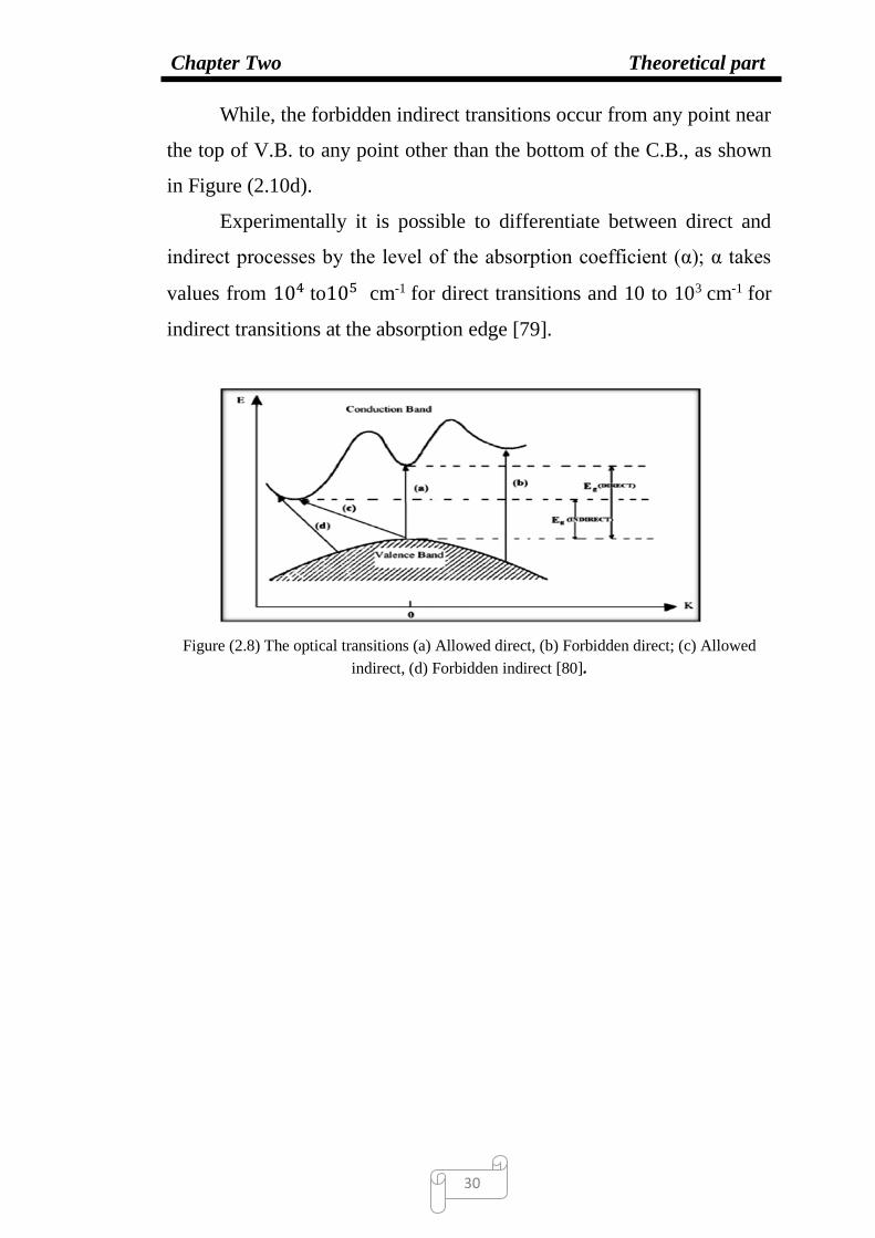
2.7.2 Direct Transitions
The direct transition in general occurs between top of valence
band and bottom of conduction band (vertical transition) Figure (2-10) at

Chapter Two Theoretical part
29
the same wave vector (Δk = 0) for conservation of momentum. The
allowed direct transition Figure(2-10a) refers to that transition which
occurs between top of the valence band and bottom of the conduction
band when the change in the wave vector equal to zero (Δk = 0).
This transition is described by the following relation [76].
𝛼ℎ𝑣 = 𝐵(ℎ𝑣 − 𝐸𝑔)1/2 (2-44)
Where B constant is inversely proportional to amorphusity.
hν is the photon energy.
Eg : is the band gap.
If the transition occurs between states of the same wave vector,
but the wave vector does not equal to zero, the transition is called
forbidden direct transition Figure (2-10b), it obeys the following relation
[77]:
𝛼ℎ𝑣 = 𝐵(ℎ𝑣 − 𝐸𝑔)3/2 (2-45)
2.7.3 Indirect Transitions
In indirect transition there is a large momentum difference
between the points to which the transition takes place in valence and
conduction bands, this means that the conduction band minimal are not
at the same value of K as the valence band maxima, then, assistance of a
phonon is necessary to conserve the momentum, therefore:
ℎ𝑣 = 𝐸𝑔 ± 𝐸𝑝 (2-46)
Where Ep is the energy of an absorbed or emitted phonon. For an
allowed indirect transition, the transition occurs from the top of the
valence band to the bottom of the conduction band as shown in Figure
(2.10c) so that [78]:
𝛼ℎ𝑣 = 𝐵(ℎ𝑣 − 𝐸𝑔)2 (2-47)
Chapter Two Theoretical part
30
While, the forbidden indirect transitions occur from any point near
the top of V.B. to any point other than the bottom of the C.B., as shown
in Figure (2.10d).
Experimentally it is possible to differentiate between direct and
indirect processes by the level of the absorption coefficient (α); α takes
values from 104 to105 cm-1
for direct transitions and 10 to 103 cm-1
for
indirect transitions at the absorption edge [79].
Figure (2.8) The optical transitions (a) Allowed direct, (b) Forbidden direct; (c) Allowed
indirect, (d) Forbidden indirect [80].

Chapter Three
Experimental Work

Chapter Three Experimental Work
31
3.1 Introduction
This chapter describes the experimental procedure and the basic
principle of the various physical techniques used to synthesize and
studying the properties of ZnO nanoparticles colloidal solution. In
addition, then studying of the preparation condition of ZnO in PLA
method with different liquid, and in spin coating environment. Figure
(3.1) show the steps of this work.
Figure (3.1):The Diagram of experiment steps of research under studying.
Structural Properties
EDX SEM XRD
Optical Properties
UV- Visible
Substrate Cleaning
Glass and P Si (electrochemical)
Substrates
Spin coating (sol gel)
Zn: MEA with
Methanol
Pulse laser ablation (PLA)
Zn target with Methanol and Distilled
water colloidal solution
Energy
effect
Type of
substrate
Type of
solvent
Laser Pulse
effect
Condition
ZnO Sample characterization

Chapter Three Experimental Work
32
3.2 Substrates Preparation and Cleaning
In present work, glass and porous silicon have been used as a
substrate, The description of the preparation of these substrates will be
mention more details in the next two section.
3.2.1 Glass Substrate
Glass substrate is used to deposit ZnO thin films with dimensions
(2.5×2.5) cm2.The cleaning of the substrate is very important because it
has a great effect on the properties of the films. The process can be
summarized by the following steps:
1. Using tap water to remove any dust that might be on the surface of
the substrates and then placed them in distilled water for 60
minutes.
2. Immersing the substrates in a pure acetone solution, which reacts
with contamination such as grease and some oxides, this process,
is fulfilled accurately by rewashing the substrates in the ultrasonic
bath for 10 minutes.
3. Drying the slides by wiping them with soft paper.
3.2.2 Porous Silicon(PSi) Substrates
The silicon wafer was n-type (111) orientation with
(1.5-4) Ω.cm resistivity and (300 ± 15 µm) thickness. cut to
Square-shaped of single crystal silicon substrates, each of (1x1) cm2
area. The silicon (Si) samples were cleaned by Radio cooperation of
America (RCA) and then by alcohol with ultrasonic bath in order to
remove the impurities and residuals and to remove the native oxide
from their surface. in order to make porous silicon substrate,

Chapter Three Experimental Work
33
electrochemical etching method (ECE) has been used. The
electrochemical etching cell is the important part of the fabrication
system as the homogeneity of Pours silicon (PSi) samples depends on
its structure. The electrochemical etching ECE cell, used in this work,
is schematically in Figure (3.2).
Figure (3.2): (a) Schematic of porous silicon set-up (b) the electrochemical etching cell.
The PSi formed under conditions 30 min of time with 1:3 mixture
of HF concentration 50% with ethanol and current densities 20–25
mA/cm2. All these requirements were considered as effective parameters
in the ECE process.
3.3 Zn Target and Colloidal Solution
The solid Zn target was taken from Fluka company ,(united-states,
product in 2015). with high purity 99.999%. The sheet of Zinc cut into
small piece with dimensions of (2×2) cm2 after that immersion the target
in the solution used.
-a- -b-

Chapter Three Experimental Work
34
3.4 Laser Ablation System
Figure (3.3) shows the experimental setup for synthesis of ZnO
nanoparticles. Glass container was applied as a cell, and the Zn target
placed on the bottom of this container filled with 3 ml of distilled water
or other solution. The cell holder rotates of 9 rpm to provide uniform
ablation and to avoid formation of a deep ablation trace due to repeated
laser pulses on same spot to help mix the solution as well. The laser
ablation process, which includes Nd:YAG laser of wavelength 1064 nm
or 532 nm, type of solvent, type of substrate and laser energy used. The
ablation process is done at room temperature. The target (Zn) (purity of
99.99%) has been immersed in water or aqueous solution, and fixed at
bottom of glass vessel container. The parameters, which effect on the
quality of thin films prepared in this method stated briefly, as following:
Figure (3.3): Experimental setup for nanoparticles synthesis by PLA process [82].
3.4.1 Laser Ablation Source
Nd:YAG laser system type Huafei providing pulses at 1064 nm
wavelength who was used as source for ablation of Zn target. Different
laser energies per pulses of (600,700 and 800) mJ, pulse duration is 10

Chapter Three Experimental Work
35
ns, repetition rate of 1Hz, effective beam diameter of 4.8 mm and the
number of laser pulse of 1000, 1500 and 2000 pulses have been used in
this work.
3.4.2 Solution Types
In present work, distilled water (DW), and methanol have been
used as a solvents.
3.4.2.1 Distilled Water
Distilled water (DW) represents a base medium for all samples
and solution to produce nanoparticles in this work. Even such water is
entirely pure; however, it is contaminated by salts ions, dissolved gases
and dissolved materials. Distilled water was prepared in our laboratory in
glasses containers to avoid the contamination
3.4.2.2 Methanol Solution
Absolute methanol (with purity 96%) was used as ablation
medium in this study. Compared to other solvents, methanol provides a
relatively inert environment for the production of nanoparticles. In
addition, it has special property to exclude the oxide layer and to
prevent the nanoparticles from oxidation.
3.5 Preparation ZnO thin film using Sol gel technique
In regard with spin coating method, the solution prepared by
mixed of zinc acetate as solvent and monoethanol amine MEA as
stabilizer of ratio 4:1 dissolved in 50 ml ethanol. To make sure that the
solution is homogeneous, the solution treatments using magnetic stirrer
and hot plate at temperature of 80 C for 1hour.

Chapter Three Experimental Work
36
3.6 The Characterization Instruments
The structural properties using XRD, Scanning electron
microscopy (SEM), Energy dispersive X-ray (EDX) have been
characterized. In addition, the optical properties using UV-Visible
spectrometer have been studied, as following:-
3.6.1 Instrument used for Structural Properties Analysis
3.6.1.1 XRD Measurement
In order to explain the structural properties, the nature and the
crystal growth of the deposited films, X-ray diffraction measurement had
been done according to either the ASTM (American Standard of Testing
Materials) or JCPD cards no. 36-1451 using Philips PW 1050 X-ray
diffract meter of 1.54 A° from Cu- kα. By using XRD result the
crystalline size (D) and FWHM could estimate and calculated using eq
(2.38).
3.6.1.2 Scanning Electron Microscope (SEM)
In this study the (SEM) a scanning electron microscopy
(INSPECT S50) equipped with energy dispersive X-ray. According to
the microscope specifications, resolution up to 7.0 nm at 3 KV (in high
vacuum mode) ensured, while magnification reported to be in the range
of 13-1000000X; though, these data is dependent on the characteristic of
each sample. It can be different depending on the sample components
like samples with heavier elements lead to obtaining analysis that is
much more accurate.

Chapter Three Experimental Work
37
3.6.1.3 Energy Dispersive X-ray (EDX)
In this study, the EDX analysis software was sourced from Oxford
Instruments Analytical Ltd. and was used to identify the elements in the
samples. All measurements were performed at an accelerated voltage of
10 kV. The electron beam current was controlled by adjusting the spot
size of the beam using the SEM control.
3.6.2 Instrument Used for Optical Properties Analysis
A double –beam UV-IR 210A Spectrophotometer is used to measure
the transmittance and absorption of ZnO film deposited at different
conditions within the wavelength range (300-900 nm) by using the data
given from this instrument, the absorption coefficients and transmission
have been calculated [83].
3.7 Thickness Measurement
In these work measured the film thickness which using SEM
method; this method was used to get the sample which was broken and
coated with gold for nonoconductive substrate. SEM micrographs of the
cross section of thin films at a tilt angle of 80 degrees where the sample
was mounted with the film on top.

Chapter Four
Result and Discussion
Chapter Four Result and Discussion
38
4.1 Introduction
In present chapter, firstly, the antireflection film with zero
reflectance condition have been design and the optical performance of
glass substrate examined using UV-V spectroscopy. Then, the structural
and optical properties of ZnO nanoparticles deposits on glass and Psi
substrates using PLA and Sol-Gel techniques have been discussed. The
effect of laser pulses number of 1000, 1500, and 2000 pulse at energies
of 600, 700 and 800 mJ with methanol and distilled water solvent have
also been studied. Over the results, the work divided into two main parts:
design of single antireflection coating layer and structural and optical
properties of the prepared films, which could divided into three sub-parts
too: preparation techniques (PLA and sol-gel), laser ablation conditions
(number of pulses, energy, and solvent type), and substrates type (glass
and PSi) as following:-
4.2 Single layer
Antireflection coating system (SL-ARCS) used to obtain zero
reflection condition of signal layer design, the modified characteristic
matrix have been employed (see section 2.4 ) . For this purpose, the
design wavelength (λd) was selected to be 1064 nm and the incident
beam consider to be normal, then the theoretical reflection values of
uncoated and coated with ZnO film on (glass and silicon substrates) are
calculated depend on the following equation [84] :
𝑹 = (𝒏𝟎−𝒏𝒔
𝒏𝟎+𝒏𝒔)𝟐 For uncoated substrate (4.1)
and
𝑹 = (𝒏𝟎𝒏𝒔−𝒏𝟏
𝟐
𝒏𝟎𝒏𝒔+𝒏𝟏𝟐)
𝟐
For coated substrate with film (4.2)
Where R: represent to the reflection, no: the air refractive index , ns:
substrate refractive index and n1: film refractive index

Chapter Four Result and Discussion
39
The reflection values of both cases are formulated in Table 4.1 as shown
below where, the refractive index of glass and silicon are 1.52 and 3.4 at
wavelength of 550 nm.
Table (4-1):
Theoretical reflection results of uncoated and coated with ZnO film
substrates
Structure Reflection Remark notice
Glass substrate 4% Satisfied zero reflection of
glass eq (4.1) without coated
Si substrate 30% Satisfied zero reflection of
glass eq (4.1) without coated
ZnO/glass substrate 20% Satisfied zero reflection of
glass eq (4.2) for coated
ZnO/Si substrate 0.6% Satisfied zero reflection of
glass eq (4.2) for coated
Note that ZnO deposited on PSi substrate gives better results than
glass substrates due to convergence of refractive index between ZnO and
silicon.
In this work, ZnO thin film used as antireflection layer (AR𝐶𝑠)
with optical path (nd) equal to quarter wavelength (λ/4) or multiply it.
Thus, the thickness measured to be 100 nm for film deposited on glass
and PSi substrates depend on [85]:
𝑛𝑑 = 𝜆/4 So, d=λ/4n (4.3)
The transmittance curve as function of wavelength shown in Figure (4.1)

Chapter Four Result and Discussion
40
Figure (4.1): Transmission curve as a function of wavelength of ZnO thin film on glass
substrate.
4.3 Structural Results of ZnO ARCS
The effect of fabrication conditions such as laser system
parameters including the influence of laser pulses number, energy,
solvent type, and substrate type on the structural properties of ZnO
nanoparticles prepared using PLA and sol-gel techniques have been
studied. These effects characterized using XRD analysis to study the
structure nature of prepared films and corresponding properties such as,
prefer diffraction peak, lattice parameters, FWHM, crystalline size,
strain and dislocation density. As well as, the morphology of the surface
of prepared films have been characterized using SEM, and EDX
spectroscopies.
4.3.1 X-Ray Diffraction (XRD) Results of ZnO Nanoparticle
by PLA Technique
Firstly, the PLA technique used to prepare ZnO nanoparticle and
related parameters will study as following:

Chapter Four Result and Discussion
41
4.3.1.1 The effect of laser pulses number
Figure (4.2) show the XRD pattern of ZnO nanoparticle on glass
substrate with laser pulses number of 1000, 1500, and 2000 pulse at
energy of 700 mJ in methanol and distilled water. This Figure revealed
that the ZnO films have hexagonal polycrystalline structure nature with
lattice parameter of samples dissolve in methanol c=5.130, 5.128 and
5.200, respectively and of samples dissolve in distilled water c= 5.179,
5.262 and 5.217, respectively. Figure (4.2.a) show that the diffraction
peaks of ZnO nanoparticle in methanol on glass substrate were at 34.42 ,
36.25 and 47.53 , which corresponding to the orientations of (0 0 2),
(101) and (1 0 2) . Figure (4.2.b) show that the diffraction peaks of ZnO
nanoparticle in distilied water on glass substrate were at 34.42 , 36.25 ,
47.35 , 56.60 and 66.37 , which corresponding to the orientations of (0 0
2), (1 0 1), (1 0 2), (1 1 0), and (1 1 2). The discussion of XRD results
will depend on the prefer orientation (0 0 2) ZnO. The increasing in the
intensity of the peaks of sample prepared in PLA method on 1000,1500
and 2000 pulses by methanol and distilled water solution attributed to the
increasing in crystal structure (crystility) of decreasing of the defect with
in the structure. The position miller indices, lattice constant, FWHM,
crystalline size and dislocation density of the above condition have been
summarized in Table (4.2)
-a-

Chapter Four Result and Discussion
42
-b-
Figure (4.2): The XRD pattern of ZnO nanoparticle on glass substrate with laser pulses
number of 1000, 1500, and 2000 pulse at energy 700 mJ a- methanol solvent b- distilled
water solvent.
4.3.1.2 The effect of laser energy
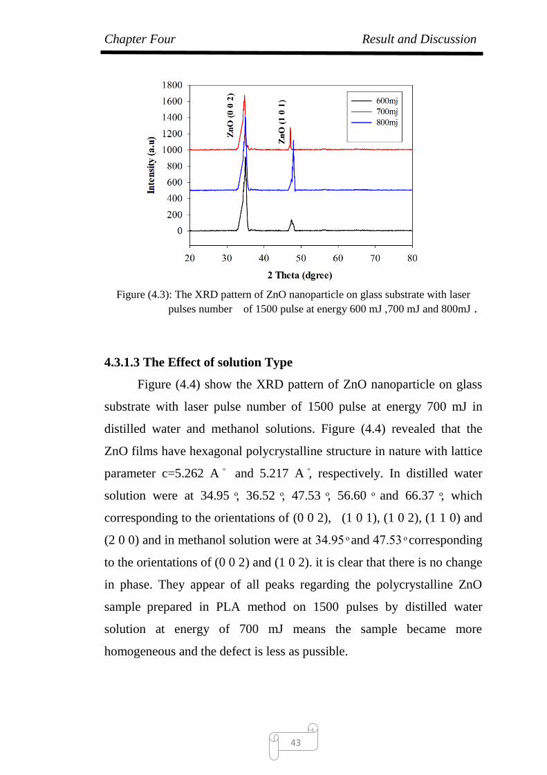
Figure (4.3) shows the XRD pattern of ZnO nanoparticle on glass
substrate with laser pulse number of 1500 pulse for energies of 600, 700
and 800 mJ dissolved in methanol. This Figure revealed that the ZnO
films have hexagonal polycrystalline structure nature with lattice
parameter c=5.230A , 5.128 and 5.137A respectively. The diffraction
peaks were at 34.90 and 36.17 A , which corresponding to the
orientations of (0 0 2), and (1 0 1). it is clear that there is no change in
phase and the optimal energy was at 700 mJ.
Chapter Four Result and Discussion
43
Figure (4.3): The XRD pattern of ZnO nanoparticle on glass substrate with laser
pulses number of 1500 pulse at energy 600 mJ ,700 mJ and 800mJ .
4.3.1.3 The Effect of solution Type
Figure (4.4) show the XRD pattern of ZnO nanoparticle on glass
substrate with laser pulse number of 1500 pulse at energy 700 mJ in
distilled water and methanol solutions. Figure (4.4) revealed that the
ZnO films have hexagonal polycrystalline structure in nature with lattice
parameter c=5.262 A and 5.217 A , respectively. In distilled water
solution were at 34.95 , 36.52 , 47.53 , 56.60 and 66.37 , which
corresponding to the orientations of (0 0 2), (1 0 1), (1 0 2), (1 1 0) and
(2 0 0) and in methanol solution were at 34.95 and 47.53 corresponding
to the orientations of (0 0 2) and (1 0 2). it is clear that there is no change
in phase. They appear of all peaks regarding the polycrystalline ZnO
sample prepared in PLA method on 1500 pulses by distilled water
solution at energy of 700 mJ means the sample became more
homogeneous and the defect is less as pussible.

Chapter Four Result and Discussion
44
Figure (4.4): The XRD pattern of ZnO nanoparticle on glass substrate with laser pulses
number of 1500 pulse at energy 700 mJ in distilled water and methanol solvents.
4.3.1.4 The effect of substrate type
Figure (4.5) show the XRD pattern of ZnO nanoparticle on glass
and PSi substrates respectively, with laser pulses number of 1500, pulse
at energy 700 mJ in distilled water solution. Figure (4.5) revealed that
the ZnO films have hexagonal with lattice parameter c=5.128 A and
5.217 A for a sample prepared on glass and PSi substrates respectively.
This Figure show that the diffraction peaks of ZnO nanoparticle on glass
substrate were at 34.95 , 36.25 , 47.53 , 56.60 and 66.37 , which
corresponding to the orientations of (0 0 2), (1 0 1), (1 0 2) , (1 1 0), and
(2 0 0). And on PSi substrate were at 34.95 and 56.60 which
corresponding to the orientations of (0 0 2) and (1 1 0). These results is
agreement with those given in JCPD data card no. 36-1451 and it is clear
that there is no change in phase for all peaks expected for (1 1 0) which
may be because the effect of created a heating treatment depending on
substrate type.

Chapter Four Result and Discussion
45
Figure (4.5): The XRD pattern of ZnO nanoparticle on glass and Si substrates
prepared using PLA method with laser pulses number of 1500 pulse at energy 700
mJ dissolved in distilled water solution.
4.3.2 X-Ray Diffraction (XRD) Results of ZnO Nanopartical
by Sol-Gel Technique
Secondly, the Sol-Gel method used to prepare ZnO nanoparticle
on glass and PSi substrates with concentration ratio of zinc acetate to
monoethanolamain (MEA) was 1:4, 3000 rotation per minutes for 30
second have been compared with that prepared using PLA technique.
Figure (4.6a) revealed that the ZnO films have hexagonal polycrystalline
structure in nature with lattice parameter c=5.199 and 5.206 for sample
prepared on glass and PSi substrates respectively. In addition the XRD
peaks of 34.475, 36.17, 47.57, and 56.17 which correspond to
orientation (0 0 2), (1 0 1), (1 0 2), and (2 0 0) respectively of ZnO thin
film on glass substrate. Theses peaks confirmed that the films are
polycrystalline in nature .Figure (4.6b) show the XRD peak of 34.425,
36.17, 47.57, and 66.73 which correspond to orientation (0 0 2), (1 0
1), (1 0 2), and (2 0 0) respectively of ZnO thin film on PSi substrate.
These results revealed that the phase between the glass and PSi

Chapter Four Result and Discussion
46
substrates has no changed. All these result in regarding the previous sub
section are summarized in Table (4-1).
Figure (4.6): The XRD pattern of ZnO nanoparticle a- on glass and b- on PSi
substrates prepared using sol gel method.

Chapter Four Result and Discussion
47
Table (4-2): The obtained result of the XDR for ZnO nanoparticles at
different (pulse, energy, solvent, method).

Chapter Four Result and Discussion
48
In summary and depend on the results especially on table (4.1), it is
possible to conclude that the best method to preaper ZnO was PLA
method with the optimal condition of preparation parameters were laser
energy of 700 MJ, laser pulses of 1500 pulse and methanol solution. In
addition, the using of P-Si as substrate was the best a recommended with
glass substrate.
4.4 Scanning Electron Microscopes (SEM) Results
Figure (4.7) show SEM images of ZnO nanoparticle prepared
using PLA with pulse laser ablation, at fixed energy of 700 mj and
different pulses of 1000, 1500 and 2000 dissolved in methanol solution
and deposition on glass substrate. It clear that the structure became as
island and then cracking observed with increases the pulse number
which attributed to interact of laser pulses with surface and may be
reformed it by reconstructed the atom on the surface. The partials size
was in nanoscale and it is seem like (cluster) at pulse number of 1500
which confirmed the XRD results.

Chapter Four Result and Discussion
49
-a-
-b-
-c- Figure (4.7): SEM images of ZnO thin film on glass substrate prepared using PLA method
in methanol solvent with energy 700 mj and pulses of a- 1000, b-1500, and c-2000 pulses
with scaling bar of 10 μm

Chapter Four Result and Discussion
50
4.4.1 Thickness Measurement
The thickness of the ZnO film prepared of 1500 pulse with 700
mJ, has been measured using cross section of SEM image as shown in
Figure (4.8) the average of thickness of film was 563 nm for all samples
used. These result is agreement with the theoretical calculation in
regared with design of single layer and with the weight method.
Figure (4.8): SEM cross section of ZnO thin film.
Figure (4.9) shows the EDX analysis which confirmed that the Zn and O
elements are including in the prepared films on glass substrate using
PLA method with energy of 700 mJ and at a- 1000 , b- 1500 , c- 2000
pulses in methanol solution.

Chapter Four Result and Discussion
51
Figure (4.9): EDX analysis of ZnO thin films prepared by PLA method on glass
substrate with energy 700 mj at pulses a-1000, b-1500 and c-2000 pulses in methanol
solvent
Figure (4.10) show SEM images of ZnO nanoparticle prepared
using PLA with pulse laser ablation, at fixed energy of 700 mJ and
different Pulses of 1000, 1500 and 2000 dissolved in distilled water
solution on glass substrate. It clear that the surface become spongy at
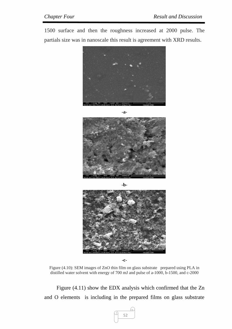
Chapter Four Result and Discussion
52
1500 surface and then the roughness increased at 2000 pulse. The
partials size was in nanoscale this result is agreement with XRD results.
-a-
-b-
-c-
Figure (4.10): SEM images of ZnO thin film on glass substrate prepared using PLA in
distilled water solvent with energy of 700 mJ and pulse of a-1000, b-1500, and c-2000
Figure (4.11) show the EDX analysis which confirmed that the Zn
and O elements is including in the prepared films on glass substrate

Chapter Four Result and Discussion
53
using PLA method with energy 700 mj and pulse number of at
1000,1500 , and 2000 pulses in distilled water solvent.
Figure (4.11): EDX analysis of ZnO thin films prepared by PLA method on glass
substrate with energy of 700 mj and at pulse number a-1000, b-1500, and c-2000 pulses
in distill water solvent.
Figure (4.12) show SEM images of ZnO nanoparticle prepared on
glass substrate using PLA with energy of 600, 700 and 800 mJ at pulse
number of 1500 pulse, dissolved in methanol solution. It clear that the

Chapter Four Result and Discussion
54
partials size is formed in nanoscale especially at energy 700 mJ which
seem like (flower) structure We have more uniform nanoparticles in this
case [31], while, at 600 mJ the surface look with various crystalline size
and at 800 mJ the surface became more sponge with pore size in range of
100-1000 nm.This result is agreement with XRD results and open the
door for more studies on this behavior.

Chapter Four Result and Discussion
55
-a-
-b-
-c-
Figure (4.12): SEM images of ZnO thin film on glass substrate prepared using PLA
at pulse number of 1500 and with energy of a-600, b-700 and c-800 mJ
in methanol solution.

Chapter Four Result and Discussion
56
Figure (4.13) show the EDX analysis which confirmed that the Zn and O
elements is including in the prepared films on glass substrate using PLA
method with energy of 700 mJ and at a- 1000, b- 1500 and c- 2000
pulses in methanol solution.
Figure (4.13): EDX analysis of ZnO thin films prepared by PLA method on glass
substrate with energy of a-600 ,b-700, and c-800 mj in methanol solution.

Chapter Four Result and Discussion
57
Figure (4.14) show SEM images of ZnO thin film prepared using
PLA with pulse laser ablation, with fixed energy of 700 mj and at
Pulse 1500 dissolved in methanol solution, porous silicon substrate. It
clear that the surface have pores with different size and different wall in
surround and partials size was in nanoscale.this result is agreement with
XRD results.
Figure (4.14): SEM images of ZnO thin film on Psi substrate prepared using PLA
with pulse 1500 and energy 700 mJ in methanol solvent.
Figure (4.15) show the EDX analysis which confirmed that the Zn and O
elements is including in the prepared films by PLA method on PSi
substrate of methanol solvent.
Figure (4.15): EDX analysis of ZnO thin films prepared by PLA method of P Si substrate in
methanol solvent.

Chapter Four Result and Discussion
58
Figure (4.16) show SEM images of ZnO nanoparticle prepared
using sol gel method. The surface morphology of fabricated ZnO thin
films on silicon substrate have smooth with light and dark color in
compared with that film on glass substrate and sample on glass substrate
have many folded which attributed to the high mismatching between the
epilayer and substrate.
-a-
-b-
Figure (4.16): SEM images of ZnO thin film on a-glass substrate b-p si substrate
prepared with sol-gel method with (3000) rotation through 10 minute.

Chapter Four Result and Discussion
59
Figure (4.17) show the EDX analysis which confirmed that the Zn
and O elements is including in the prepared films on both glass and
silicon substrate
Figure (4.17): EDX image of ZnO thin films a-Glass substrate b- pSi substrate
prepared using spin coating (sol gel) method
4.5 Optical Properties
The optical properties of the transparent conducting films depend
mainly on the deposition techniques and the preparation conditions in
this section the optical properties of ZnO thin films on glass substrate
prepared using PLA and sol gel techniques have been discussed. by UV-
Vis spectrophotometer are studied in the wavelength range from 200 nm

Chapter Four Result and Discussion
60
to 1100 nm, and study the effect of the laser pulses number, laser energy
and solvent type on the optical properties of the prepared samples.
4.5.1 Effect of pulses number
The effect of the pulse number with 1000, 1500 and 2000 pulses of
methanol and distilled water solutions on ZnO thin films is shown in
Figure (4.18). It is found that the films have high transmission at long
wavelengths reach to (90%) in the visible region. The optical
transmission of ZnO thin films found to be decreases with increasing
Pulses laser in methanol solution while the optical transmission of ZnO
thin films found to be increasing with increases pulses laser in distilled
water solution, which Attributed to satisfy the zero reflectance condition
and the film became more transparent in regard with pulse.
Figure (4.18): Transmittance spectra as function of wavelength of ZnO thin films at
different Pulses number of 1000, 1500 and 2000 dissolved in a- methanol solvent and b-
distill water solvent .
High transmittance in distilled water solution indicates that the obtained
films are of low impurities and have only few lattice defects [86]
Figure (4.19) show the effect of different laser pulse number with
different type of solution. The different pulse in methanol solution It is
found that the band gab energy increases with the increasing of laser

Chapter Four Result and Discussion
61
pulse number but in distilled water the energy band gap decrease with
increased pulses.which mean that the blue shift of energy band gab is
obtained . The energy band gap values depend in general on the film
crystal structure, the arrangement and distribution of atoms in the crystal
lattice also affected by crystal regularity. Attributed to the defect and
high confinement effect since the structure going to be in nano scale in
Table (4.3)
Figure (4.19): APlots of ( hν)2 verses photon energy (hν) of doped ZnO thin films
at different of pulses number a- methanol solvent b- distilled water solvent.
Table (4.3):
Experimental result for different pulse laser number.
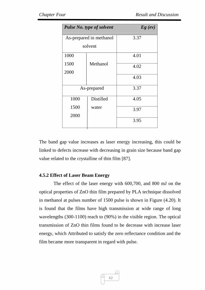
Chapter Four Result and Discussion
62
Pulse No. type of solvent Eg (ev)
As-prepared in methanol
solvent
3.37
1000
1500 Methanol
2000
4.01
4.02
4.03
As-prepared 3.37
1000 Distilled
1500 water
2000
4.05
3.97
3.95
The band gap value increases as laser energy increasing, this could be
linked to defects increase with decreasing in grain size because band gap
value related to the crystalline of thin film [87].
4.5.2 Effect of Laser Beam Energy
The effect of the laser energy with 600,700, and 800 mJ on the
optical properties of ZnO thin film prepared by PLA technique dissolved
in methanol at pulses number of 1500 pulse is shown in Figure (4.20). It
is found that the films have high transmission at wide range of long
wavelengths (300-1100) reach to (90%) in the visible region. The optical
transmission of ZnO thin films found to be decrease with increase laser
energy, which Attributed to satisfy the zero reflectance condition and the
film became more transparent in regard with pulse.

Chapter Four Result and Discussion
63
Figure (4.20): Transmittance spectra of ZnO thin films at different laser energy with
600,700 and 800 mj of methanol solvent.
Figure (4.21) show the direct band gap values for ZnO thin film
at different laser beam energy with 600, 700 and 800 mJ. The band gap
value increases as laser energy decreasing, this could be linked to defects
decrease with increasing in grain size because band gap value related to
the crystalline of thin film also this due to formation of sub band
between the band gap and conduction band [34]. as shown in Figure
(4.21) and these results summarized in table (4-4).
Figure (4.21): APlots of ( hν)2 verses photon energy (hν) of doped ZnO thin films
at different laser energy.

Chapter Four Result and Discussion
64
Table (4-4): Experimental result for different laser energy.
Laser beam energy (mJ) Eg(ev)
As-prepared 3.37
600 4.06
700 4.02
800 4.01
4.5.3 Effect of Solution Type
Figure (4.22) show the effect of solvent type of ZnO on the optical
performance. It clear that the films have high transmission at long
wavelengths reach to (90%) in the visible region. The optical
transmission of ZnO thin films found to be decreases in methanol solvent
while increase in distilled water solvent, which attributed to satisfy the
zero reflectance condition and the film became more transparent in
regard with pulse.
Figure (4.22): Transmittance spectra of ZnO thin films at different solvent type
(methanol and distill water) solvent respectively.

Chapter Four Result and Discussion
65
The energy bang gap of methanol and distill water solvent as
function of (αh𝑣)2 has been examined. The results revealed that the value
of energy band gap have blue shift toward the high energy band gap
which attributed to the defect through the synthesis and may be high
confinement effect occurred, since the structure became in nanoscale as
mention in SEM results. These results show in Figure (4.23) and
summarized in Table (4.5).
Figure (4.23): A plots of ( hν)2 verses photon energy (hν) of doped ZnO thin films
of different solvent type.
Table (4-5):
Experimental result 2000 pulse of different solvent.
2000 pulse of solvent type Eg(ev)
As-prepared 3.37
2000 pulse in methanol 4.03
2000 pulse in distill water 3.95

Chapter Four Result and Discussion
66
4.6 Optical Properties Results of ZnO Nanopartical by Sol-
Gel Technique
In sol gel method the optical properties founded the substrate
coated have high transmission at wide range of long wavelengths (300-
1100) reach to (90%) in the visible region Compared with uncoated.
attributed to satisfy the zero reflectance condition and the film became
more transparent in regard in comparison with uncoated substrate.as
shown in Figure (4.24).
Figure (4.24): Transmittance spectra of ZnO thin films in case of coated and uncoated the
substrate.
The energy bang gap of spin coating method as function of (α h𝑣)2
has been examined. The results revealed that the value of energy band
gap have blue shift toward the high energy band gap which attributed to
the defect through the synthesis and may be high confinement effect
occurred, since the structure became in nanoscale as mention in SEM
results. These results show in Figure (4.25)

Chapter Four Result and Discussion
67
Figure (4.25): A plots of ( hν)2 verses photon energy (hν) of doped ZnO thin films in sol
gel method.

47
Table (4.2): The obtained result of the XDR for ZnO nanoparticles at different (pulse, energy, solvent, method).
Structure Method to
prepare Solvent type
Energy
(mJ)
Pulses
Position (2
theta) (hkl)
Lattice
constant (c)
(nm)
FWHM Crystalline size
(nm) Strain
Dislocation
density
Zno/glass
PLA
Methanol
700 mJ
1000
34.85
(002) 5.130902 0.055721 81.83035 0.004234 0.000149
1500 34.95
(002) 5.12838
0.05721 79.47251 0.00436 0.00015833
2000 34.45
(002)
5.200524 0.041883 110.1309
0.003146 0.00082443
ZnO/glass
Distilled
water
700 mJ
1000 34.74 (002) 5.179515
0.05364 135.9722 0.002548 0.00054087
1500 34.05 (002) 5.26235
0.05016 193.03823 0.003724 0.0001155
2000 34.35 (002) 5.217756 0.0643 323.4993 0.001071 0.0009555
ZnO/glass
Methanol
600 mJ
1500
34.90 (002) 5.230902 0.05321 85.56919 0.004049 0.000136573
700 mJ 34.95 (002) 5.12838
0.05721 79.47251 0.00436 0.00015833
800 mJ 34.75 (002)
5.12838
0.03721 122.8914 0.00282 0.0006621
ZnO/glass
Sol -gel
-
-
-
34.475 (002) 5.1994 0.0476 96.833333 -0.003578 0.000106647
ZnO/Si 34.425 (002) 5.2067 0.05420 85.16533 0.004069 0.00013781

Chapter Five
Conclusion and
Future Works

Chapter Five Conclusion and Future Works
68
5.1 Conclusion
Zinc oxide thin film has been successfully prepared on glass and PSi
substrates using Pulse laser ablation (PLA) and sol gel methods. The
prepared films have hexagonal structure with preferred orientation
(0 0 2) and polycrystalline in nature. Additionally, narrow FWHM, low
strain and small crystalline size have been obtained. Crystalline size of
ZnO dissolved in methanol have been increased with increasing in the
Number of laser pulse at fixed of 700 mJ. While, low crystalline size of
ZnO dissolved in distilled water at fixed laser pulse of 1500 pulse was
obtained at energy of 700 mJ. In addition, the crystalline size of ZnO
thin film on glass and PSi substrates were 96.833 nm and 85.165 nm,
respectively.
Homogenous film with some cluster and Island, and then the cracking
started with increasing of the laser pulses for all cases, expected that the
film on glass substrate using PLA method with methanol as a solvent,
energy of 700 mJ and pulses of 1500 pulse which revealed Nanostructure
like tree leaf. All prepared thin film are free of impurities and
contaminations.
All the samples on glass substrates have smooth morphology with
transparent in range of 300-800 with high optical band gap energy of
3.37 eV with blue shift toward short wavelength.
5.2 Future works
1- Study the electrical properties of the prepared films.
2- Design of double and multilayer antireflection coating using ZnO.
3- Design single layer antireflection coating using another material
such as ZnS and SnO2.

Chapter Five Conclusion and Future Works
69
4- Fabricate ZnO thin film using different physical techniques such
DC and RF Sputtering and pulsed laser deposition (PLD).
5- Study the annealing temperature effect on the physical properties
of films.
6- Used the films in optoelectronic application such as solar cell,
photodetectors and gas sensor.
Reference

Reference
70
Reference
[1] S. Jei Hong and J. In Han"Fabrication of Indium Tin Oxide (ITO)
Thin Film withPre-Treated Sol Coating", Journal of Korean Physical
Society ,Vol. 45, No. 3, pp. 634-637, September (2004).
[2] P. K. BISWAS, A DE, L K DUA and L CHKODA"Surface
characterization of sol–gel derived indium tin oxide films on glass",
Indian Academy of Science, Vol. 29, No. 3, pp. 323–330 June
(2006).
[3] H. Kim and Y. Kim"Characteristics of Indium-Tin-Oxide
Nanoparticles Prepared by Controlled Chemical Coprecipitation
Method", Bull. Korean Chem. Soc., Vol. 29, No. 9,)2008).
[4] F. Quarantaa, R. Rellaa and P. Siciliano et al."Preparation and
characterization of nanostructured materials for an artificial olfactory
sensing system" , Elsevier Science ,Vol. 84,pp. 55–59,(2002).
[5] M. Ivanovkaya "Gas-sensitive properties of thin film heterojunction
based on In2O3 nanocomposites" ,Elsevier Science, Vol.7031,
PP.1–9,(2003).
[6] J. T. Cox and G. Hass " Triple – layer antireflection coatingon glass
for the visible and near- infare" , J.Opt.Soc. Am. 52 (1962) 965.
[7] H.K. Pulker "Characterization of Opticalbthin film", Appl. Opt 18
(1979) 1960.
[8] K.N.Chopra, O.P.Grover, and R. Hradaynath, "Antireflection coating
effective at two wavelength simultaneously in the visible region using
homogeneously mixed dielectric", Appl. 15 (1979)1750.
[9] R.M.A.Azzam, E. Bu. Habib, J. Casset, G. Chassaing and P.
Gravier,"Antireflaction of an absorbing substrate by absorbing thin film
at normal incident", Appl. Opt. 26 (1987) 719.
[10] C.L. Negendra, M. Viswanathan, and G. K. M. Thutupalli, ''Design
and optimization of low – loss wideband antireflection coating for the
visible and infrared regions: a new method'', Appl. Opt. 14(1985) 1156.

Reference
71
[11] H. A. Macleod, Thin Flim Optical Filters (McGraw-Hill, New York,
1986).
[12] K. L. Chopra,Thin – Flim Phenmena (McGraw – Hill, New Yrk,
1989).
[13] J and W, Fundmentals of Optics (McGraw – Hill Koganasha, Ltd,
1984)
[14] A. Hashim, M. S. Jaafar, A. J. Ghazai, N. Alrawi," Fabrication and
characterization of ZnO thin film using sol–gel method". International
Journal for Light and Electron Optics 124(6):491–492 · March 2013.
[15] A. Mussetand A, Thelen, ''Multilayer antireflections, in progress in
optics'' E. Wolf, ed (North – Holland, Amsterdam,1970), Vol. 18, p p.
201-233.
[16] A. Thelen, Design of Optical Interference Coating McGraw – Hill
Compqny, New York, 1989)
[17] H. Gh. Rashid, Z. T. Al- Dahan, and H. M. Ibrahim, ''Design of dual
– band antireflection coating'', accepted in the first conference on Physics
and materials research IAEC, Baghdad, 1999.
[18] K. Robinvitch and A. Pagis ''Influence of heat treatments on the
spectral performance of a V –type double antireflection coating at 1.06
μm'', Appl. Opt. 21(1982) 2160.
[19] H. L. Hartnagel, A.L.D., A. K. Jain, and C. Jagadish,
Semiconducting Transparent Thin Films. 1995, Bristol: Institute of
Physics. 358.
[20] U.A. Ozgur, , Y. I. Liu, C. Teke, A. Reshchikov, M. A. Dogan, S.
Avrutin, V. Cho, S. J. and Morkoc, H., A comprehensive review of ZnO
materials and devices. Journal of Applied Physics, 2005. 98(4): p. 103
[21] L. Kazmarski and A. H .Clark, "Polycrystalline and Amorphous Thin
Films and Device", Edited by Lawrence Academic Press, New York,
(1980).
[22] A.V. SIngh, M. kumar, R. M. Mehra, A. Wakahara and A.Yoshida,"
Al-doped zinc oxide (ZnO:Al) thin films by pulsed laser ablation". J.
Indian Inst. Sci., Sept –Oct. 2001, 81, 527-533.

Reference
72
[23] Y. Ishikawa, Y. Shimizu, T. Sasaki and N. Koshizaki," Preparation
of zinc oxide nanorods using pulsed laser ablation in water media at high
temperature". Journal of Colloid and Interface Science 300 (2006) 612–
615
[24] Q.H. Chen and W. G. Zhang," Successive preparation of decorated
zinc oxide organic sol by pulsed laser ablation and their luminescence
characteristics". j.apsusc.2006.06.065.
[25] R.K. Thareja and S. Shukla, "Synthesis and characterization of zinc
oxide nanoparticles by laser ablation of zinc in liquid. Applied Surface
Science 253 (2007) 8889–8895.
[26] R. S. Ajimsha, G. Anoop, A. Aravind, and M. K. Jayarajz,"
Luminescence from Surfactant-Free ZnO Quantum Dots Prepared by
Laser Ablation in Liquid". Electrochemical and Solid-State Letters,
(2008), 11 (2) K14-K17.
[27] J. M. Cho, J. K. Song, and S. M. Park," Characterization of ZnO
Nanoparticles Grown by Laser Ablation of a Zn Target in Neat Water".
Bull. Korean Chem. Soc. 2009, Vol. 30, No. 7.
[28] I.S. Virt, I.V. Hadzamana, I.S. Bilyka, I.O. Rudyic, I.V. Kuriloc And
et al. "Properties of ZnO and ZnMnO Thin Films Obtained by Pulsed
Laser Ablation", Oxide Materials for Electronic Engineering” (OMEE-
2009), Vol. 117, No. 1. 2010.
[29] R. A. Ismail, A. K. Ali, M. M. Ismail, K. I. Hassoon." Preparation
and characterization of colloidal ZnO nanoparticlesusing nanosecond
laser ablation in water". 1:45–49. Appl Nanosci (2011).
[30] G Atanasova1, A Og Dikovska, M Stankova, P Stefanov1 and P A
Atanasov. " XPS study of ZnO nanostructures prepared by laser
ablation". Journal ofPhysics:ConferenceSeries 356 012036. (2012).
[31] D. Nakamura, T. SImogaki, K. Okazaki, M. Higashihata, H. Ikenoue
and et al," Synthesis of Various Sized ZnO Microspheres by Laser
Ablation and Their Lasing Characteristics". JLMN-Journal of Laser
Micro/Nanoengineering,Vol. 8, No. 3, (2013), .
Reference
73
[32] F. A. Fadhil and I. H. Hadi, " Preparation and characterization of
zinc oxide nanoparticles by laser ablation of zinc in isopropanol". Eng.
&Tech, Vol.33 , Part (B), No.5, Journal, (2015).
[33] E. T. Salim, M. A. Fakhri, ,H. Hassan, Z. T. Salim and A. Z.
Mohamed, "PhysicochemAical properties of ZnO Nanoparticles prepared
using low energy low repetition rate Laser system" . Sci.Int. (Lahore),
28(5), 4501-4506(2016).
[34] S. V. Farahan, A. Mahmood and M. Goranneviss, " The effect of
laser environment on the characteristics of ZnO nanoparticles by laser
ablation". Int Nano Lett 6:45–49, (2016).
[35] R. A. Ismail, N. F. Habubi, E. H. Hadi, "Synthesized and
characterization of pure and Er+3 doped ZnO nanoparticles by using laser
ablation in ethanol". World Scientific News 33 67-78(2016), .
[36] K. S. Khashan and F. Mahdi, " Synthesis of ZnO: Mg
Nanocomposite by Pulsed Laser Ablation in liquid". Surf. Rev. Lett. 0,
(2017), 1750101.
[37] A.R. Phani, M. Passacantando, and S. Santucci, "Synthesis and
characterization of zinc aluminum oxide thin films by sol-gel technique".
Materials Chemistry and Physics, 68, pp. 66-71, (2001).
[38] K.R. Murali, Properties of sol-gel dip-coated zinc oxide thin films.
Journal of Physics and Chemistry of Solids, 68, pp. 2293-2296,(2007).
[39] Z. Xiaofeng, J. Tao, Z. Jian and W. Xiaohua, "Humidity sensor
based on quartz tuning fork coated with sol-gel-derived nanocrystalline
zinc oxide thin film". Sensors and Actuators B,123, pp.299-305,(2007).
[40] P. Bhattacharyya, P. K. Basu, H. Saha, and S. Basu, "Fast response
methane sensor using nanocrystalline zinc oxide thin films derived by
sol-gel method". Sensors and Actuators B,124, pp. 62-67,(2007). .
[41] C. Mehmet, O. Shine, and C. Gabriel, "Sol-gel synthesis,
comparative characterization, and reliability analyses of undoped and Al-
doped zinc oxide thin film". Thin Solid Films, 517, pp. 6323-
6326,(2009). .

Reference
74
[42] C. Jagadish, and S. J. Pearton, "Zinc Oxide Bulk, Thin Films, and
Nanostructures: Processing, Properties, and Applications". Elsevier,
Netherlands. (2006).
[43] O. Shane,C. Mehmet, Paul ,T. G. Mark, A. Jeff, P. Ian et al. "The
effect of dopants on the morphology, microstructure and electrical
properties of transparent zinc oxide films prepared by the sol-gel
method". Thin Solid Films, 520, pp. 1174-1177,(2011). .
[44] M. Sathya , A. Claude, P. Govindasamy and K. Sudha."Growth of
pure and doped ZnO thin films for solar cell applications", Advances in
Applied Science Research, 3 (5):2591-2598, 2012 .
[45] L.Yang, B. Duponchel, R.Cousin, C. Gennequin, G. Leroy, J. Gest,
et al. "Structure, morphology and electrical characterizations of direct
current sputtered ZnO thin films". Thin Solid Films, 520, pp. 4712-
4716(2012).
[46] Y. Al-Douri, A. H. Reshak, W. K. Ahmed, A. J. Ghazai “Structural
and optical investigations of In doped ZnO binary compound” Materials
Express 4,159-164,(2014) .
[47] A. J. Ghazaia, E. A. Salmanb, Z. A. Jabbarc." Effect of Aluminum
Doping on Zinc Oxide Thin Film Properties Synthesis by Spin Coating
Method". American Scientific Research Journal for Engineering,
Technology, and Sciences (ASRJETS) Volume 26, No 3, pp 202-211,
(2016).
[48] A. J. Ghazai1, E. A, Salman and Z. H. ------." Structural Properties
of Zno Thin Films Prepared Using Different Techniques". Swift Journal
of Physical Sciences Vol 2(1) pp. 001-004 May, 2016.
[49] M. Born and E. Wolf, Principle of Optics, 5th – ed. Program on
London, 1975.
[50] Z. Knittle, Optics of Thin – Flim (Wily, New York, 1976).
[52] M. Aziz, S. S. Abbas and W. Rosemaria "Size-controlled synthesis
of SnO2 nanoparticles by sol–gel method", Materials Letters,Vol. 91, PP.
31–34, (2013).
[53] N. Nadaud," Structural studies of tin-doped indium oxide (ITO) and
In4Sn3O12", J. Solid State Chem, Vol. 135, No. 1, pp. 140-148, (1998).

Reference
75
[54] R.Savu, M. Adlfo and E. Joanni," grain size effect on the electrical
response of SnO2 thin and thick film gas sonsor", Materials research,
Vol.12, NO.1, P.83-87, (2009).
[55] R. Chandran and G. Suresh, "A comparative study of physical and
optical properties pf cdZnS and cdNiS Nanocrystalline films deposition
by chemical bath method", Chalcogenide Lett ., Vol.8, No.11 ,pp. 689-
694,(2011).
[56] F. O. Adurodija, L. Semple and R. Bruning, "Crystalliza- tion
Process and Electro-Optical Properties of In2O3 and ITO Thin Films",
Journal of Materials Science, Vol. 41, No. 21, pp. 7096-7102,(2006).
[57] S. A. Bashar, "Study of Indium Tin Oxide (ITO) for Novel
Optoelectronic Devices", University of London Regulations for the
Degrees of M.Phil. and Ph.D., October (1997).
[58] Y. V. Gassenbauer and A. Klein, "Electronic and Chemical
Properties of Tin-Doped Indium Oxide (ITO) Surfaces and ITO/ZnPc
Interfaces Studied In-situ by Photoelectron Spectroscopy", J. Phys.
Chem,Vol.110, pp.4793-4801,(2006).
[59] XRD picture. Available from:
http://tap.iop.org/atoms/xray/530/img_full_47305.gif.
[60] T. Ungar, Microstructural parameters from X-ray diffraction peak
broadening. Scripta Materialia 51, 777–781, (2004).
[61] G. Maeder, X-ray diffraction and stress measurements. Chemica
Scripta a 26, 23–31, (1986).
[62] P. Pourgahramani, and P. Bal´aˇz, “Structural Changes and
Characterizations in the Powder Materials Obtained From Milling
Processes. In: M. Yekeler (Ed.) Powder Technology and
Characterization. Trivandrum, Kerala, pp. 217–250, (2008)
[63] T. Berg, E. Marosits, J. Maul1, P. Nagel, U. Ott, F. Schertz, S.
Schuppler, Ch. Sudek and G. Schönhense, “Quantum Confinement
Observed in the X-ray Absorption Spectrum of Size Distributed
Nanodiamonds Extracted From the Murchison Meteorite”, Lunar and
Planetary Science XXXIX (2008).

Reference
76
[64] T. Ogawa and Y. Kanemitsu “Optical Properties of Low-
Dimensional
Materials”, Word Scientific, Singapore, (1995).
[65] S. Boninelli, “Properties and Evolution of Si Nanoclusters Studied
by Energy Filtered Transmission Electron Microscopy”, University of
Catania, Ph.D thesis, December (2004).
[66] P. Harrison, “Quantum Wells, Wires and Dots”, John Wiley & Sons,
LTD., (2004).
[67] Y. Dan, S. Evoy and A. Johnson,"Chemical Gas sensors Based on
nanowires", Arxiv preprint arXiv:0804. 4828 (2008).
[78] J. Schaffer, A. Saxena, S. D. Antolovich, T. H. Sanders Jr. and S. B.
Warner: The Science and Design of Engineering Materials, 2nd ed.,
(McGraw-Hill International, pp. 65–75, (1999).
[69] A. Alivisatos,"Semiconductor Clusters, Nanocrystals, and Quantum
Dots. Science", 271, 933-937, (1996).
[70] A. Ivashchenko , and I. Kerner , "Moldavian J. Phys. Sci. ",
"Physical Approaches to Improvement of Semiconductor Gas Sensor
Based on SnO2 Thin Films" Moldavian Journal of the Physical Sciences,
Vol. 2, N1, , PP.95-102, (2003).
[71] V. Satish, Kailas, “Material Science”, Dept. of Mechanical
Engineering, Indian Institute of Science, Bangalore, India, (2005).
[72] J. Van Berkum , A. C. Varmcuch , R. Delhen , Th. H. Dinkeijser ,
and E. J. Hemeijer , "Applicabilities of the Warren-Averbach analysis and
an Alternative Analysis for Separation of Size and Strain Broadening," J.
Appl. Crys., Vol. 27, , PP. 345-357, (1994).
[73] T. Obata , K. Komeda , T. Nakao , H. Ueba , and C. Tasygama ,
"Structural Characterization of Si0.7Ge0.3 Layers Grown on Si(001)
Substrates by Molecular Beam Epitaxy," J. Appl. Phys. Vol. 81, P.199,
(1997) .
[74] S. Hussain, "Investigation of Structural and Optical Properties of
Nanocrystalline ZnO", Thesis Report, Linköpings Universitet, (2008).

Reference
77
[75] S. T. Ngqondo , “Hydrothermally grown Pb2+ doped ZnO Nanorods
for Hydrogen and Acetylene Gas sensing” Department of Physics,
University of Zululand, 2008.
[76] C. R. Blanchard “Atomic Force Microscopy”, the Chemical
Educator, Vol. 1, No. 5, P 5059, 1996.
[77] F. Guo, B. Yang, Y. Yuan, Z. Xiao, Q. Dong, Y. Bi and J. Huang,"
A Nanocomposite Ultraviolet, 2001.
[78] J. Goldstein (2003). Scanning Electron Microscopy and X-Ray
Microanalysis. Springer. ISBN 978-0-306-47292-3. Retrieved 26 May
2012.
[79]Jump up ^ Joseph Goldstein (2003). Scanning Electron Microscopy
and X-Ray Microanalysis. Springer. ISBN 978-0-306-47292-3. Retrieved
26 May 2012.
[80] R. J. Elliot and A. I. Gibson, "An Introduction to Solid State Physics
and Application", 1st edition, Macillian Inc. (1974).
[81] R. A. Grenier, "Semiconductors Device, Electronic Energy Series",
Mc Graw-Hill, Book Co.Inc. (1961).
[82] L. Kazmarski and A.H.Clark, "Polycrystalline and Amorphouse Thin
Films and Device", Edited by Lawrence Academic Press, New York,
(1980).
[83] G. Burns, "Solid State Physics, Academic Press, Inc.", Harcourt
Brace Jovanovich, New York, (1985).
[84] M. Grundmann, H.v. Wenckstern, R. Pickenhain, Th. Nobis, A.
Rahm, M. Lorenz, "Super lattices and Microstructures", Vol. 38, , PP.
317–328, (2005).
[85] M. Lorenz, H. Hochmuth, R. Schmidt, E. M. Grund, M. Kaidashev,
Grundmann, "Advances of Pulsed Laser Deposition of ZnO Thin Films",
Ann. Phys., V. 13, , P. 59, (2004).
[86] J. Taus, "Amorphous and Liquid Semiconductors", Plenums Press,
New York and London, (1974).
[87] T. S. Moss, "Optical Properties of Semiconductors", London Butter
Worthes Scientific Puplications, (1959).

الملخص
اغشية أوكسيد لانعكاس منر طبقة مفردة من طلاء مضاد في هذا البحث تم تصميم وتحضيسامي باستخدام طريقتي القشط من الزجاج والسيليكون المالزنك النقية على ارضيات أساس
بنبضات الليزر والطلاء البرمي.
أساسيين هما الأول.. تصميم طلاء مضاد للانعكاس في طبقة مفردة جزئيينيقسم العمل الى من اغشية أوكسيد الزنك الرقيقة باستخدام المصفوفة المميزة المعدلة لتحقيق شرط الانعكاس
الصفري نظريا.
PLAوالثاني.. تحضير اغشية أوكسيد الزنك النانوية على ارضيات أساس مختلفة بطريقتي ضربة, الطاقة المستخدمة 1000,1500,2000أثير عدد الضربات والتي تضمنت دراسة ت600,700,800 mJ ونوع المذيب )ماء منزوع الايون( والميثانول, وكذلك نوع الأرضية
هذا لترسيب ( spin coating)الطلاء البرمي طريقة استخدام تم ذلك, إلى وبالإضافة الأساسي .الغشاء
المحضرة باستخدام جهاز حيود الاشعة السينية للأغشيةتم دراسة الخصائص التركيبية والبصرية (XRD( المجهر الالكتروني الماسح ,)SEM( و مطياف تشتت اشعه سينية ,)EDX ,)
على التوالي. UV-Visومطياف
التبلور مع أظهرت ان اغشية أوكسيد الزنك المحضرة هي بتركيب سداسي متعدد XRD نتائج الليزر مع نبضاتعدد زيادةلذلك فان حجم البلوري ازداد مع بالإضافة( 002اتجاه سائد )
0011باستثناء عند عدد نبضات .mJ 700ثابته كمذيب وعند طاقه و الماء الايوني الميثانول مع الميثانول كمذيب فان الحجم البلوري هنا اصبح اقل ما يمكن mJ 700 نبضه و طاقه
على ارضيات الأساس من الزجاج المترسبة الأغشية. اضافه لذلك فان وظهور حاله نانو and 85.165طريقه الطلاء البرمي تمتلك حجما بلوريا باستخداموالسيلكون المسامي
96.833) nm ) .شده أعظمصف عرض النطاق عند منت على التواليFWHM ضيق ولم يتم ملاحظه أي تغيير في الطور لجميع الحالات.

أوضحت ان الأغشية في كل الحالات كانت متجانسه SEMصور المجهر الالكتروني الماسح مع بعض الجزر والتكتلات بعدها يبدا ظهور التشققات وتزداد بزياده عدد النبضات باستثناء
mJ 700مع محلول الميثانول بطاقه PLAالغشاء المرسب على الزجاج باستخدام طريقه ه ورق الشجز.نبضه والتي أوضحت تركيبا نانويا يشب 0011وعدد نبضه
فقد بينت ان الاغشية المحضرة خالية من الشوائب وهذه النتائج تتطابق مع EDXاما نتائج .XRDالنتائج
فجوة الطاقة البصرية البصرية,الخصائص البصرية متضمنة السلوكية UV-Visوكانت نتائج ية عالية لك نفاذتومعامل امتصاص كدالة للطول الموجي أوضحت ان الاغشية المحضرة تم
مع فجوة طاقة nm 800-300بحدود والتي مداها يتراوح في المنطقة المرئية %85حدود بمع حصول انحراف باتجاه الاطوال الموجية ... عند زيادة eV 3.37بصرية كبيرة نسبيا بحدود
الضربات والطاقة.

جمهورية العراق
العلمي والبحث العالي التعليم وزارة
النهرين جامعة
العلوم كلية
قسم الفيزياء
كاسيد الزنكا منغشاء رقيق وتصنيع صميمت
مختلفة ياتتقن باستخدامللانعكاس المضاد
رسالة
النهرين جامعة \العلوم مقدمة الى كلية
الفيزياء علوم في ماجستير درجة نيل متطلبات من جزءك
قبل من
داء طه ياسينن
5002الجامعة المستنصرية بكالوريوس
بأشراف
علاء جبار غزايد. م.أ.
5002 تموز شوال 0341