DESIGN AND COMPARATIVE MATERIAL ANALYSIS OF A …
172
DESIGN AND COMPARATIVE MATERIAL ANALYSIS OF A CAPACITIVE TYPE PRESSURE SENSOR FOR MEASUREMENT OF KNEE PRESSURE DISTRIBUTION OF RODENTS by Al Maqsudur Rashid A thesis submitted in partial fulfillment of the requirements for the degree of Master of Science in Mechanical Engineering MONTANA STATE UNIVERSITY Bozeman, Montana December, 2013
Transcript of DESIGN AND COMPARATIVE MATERIAL ANALYSIS OF A …

DESIGN AND COMPARATIVE MATERIAL ANALYSIS OF A CAPACITIVE TYPE
PRESSURE SENSOR FOR MEASUREMENT OF KNEE PRESSURE
DISTRIBUTION OF RODENTS
by
Al Maqsudur Rashid
A thesis submitted in partial fulfillment
of the requirements for the degree
of
Master of Science
in
Mechanical Engineering
MONTANA STATE UNIVERSITY
Bozeman, Montana
December, 2013

©COPYRIGHT
by
Al Maqsudur Rashid
2013
All Rights Reserved

ii
APPROVAL
of a thesis submitted by
Al Maqsudur Rashid
This thesis has been read by each member of the thesis committee and has been
found to be satisfactory regarding content, English usage, format, citation, bibliographic
style, and consistency and is ready for submission to The Graduate School.
Dr. Ronald June
Approved for the Department of Mechanical and Industrial Engineering
Dr. Christopher Jenkins
Approved for The Graduate School
Dr. Karlene A. Hoo

iii
ACKNOWLEDGEMENTS
I would like to express heartfelt gratitude to my supervisor and thesis committee
chair Dr. Ron June for supporting me from the very beginning of his project with many
encouragements and ideas and suggesting me a proper path to finish my degree. It was a
wonderful learning experience for me during the work presented here with proper
guidance and mentoring from him. Without his patience I wouldn't have finish this write-
up any sooner. Then I would like to give a special thanks to my former supervisor Dr.
Ahsan Mian for introducing me to MEMS at MSU and later presenting me this work
which eventually gave the foundation of my thesis. I am thankful to Tom Rose who
allowed me to cite his experimental data and updating me with experimental
measurements from time to time during the ongoing project upon which this work was
built on. I am grateful to Harris Mousoulis from Purdue University with whom I have
shared and exchanged knowledge about various MEMS clean room process and steps.
Also thanks to Donny Zignego for showing me quick tips on how to format this report
easily. Lastly all of these would have never been possible if I wouldn’t have received
support from my parents thousands mile away from here praying for me all the time.

iv
TABLE OF CONTENTS
1. INTRODUCTION TO MEMS BASED PRESSURE SENSOR .................................. 1
Mems Pressure Sensor Overview ................................................................................. 1
Piezoresistive and Capacitive MEMS Pressure Sensor ................................................ 3
Motivation ..................................................................................................................... 6
Osteoarthritis and Contact Pressure ........................................................................ 9
Role of Knee Loading in Osteoarthritis ................................................................ 10
Mouse as Experiment Model ................................................................................ 13
2. DESIGN AND MODELING ...................................................................................... 15
Array Configuration .................................................................................................... 15
Pressure Sensor for Rodents: Initial Design ............................................................... 19
First Iteration of Design .............................................................................................. 23
Upper and Lower Polymer Layer ......................................................................... 24
Upper Electrodes ................................................................................................... 24
Lower Electrodes .................................................................................................. 26
Thin Insulation Layer With Air Pocket ................................................................ 27
Second Iteration of Design .......................................................................................... 28
Full Sensor ............................................................................................................ 29
Upper and Lower Polymer Layer ......................................................................... 30
Upper and Lower Electrodes ................................................................................ 31
Insulation Layer .................................................................................................... 32
Connecting Pads ................................................................................................... 33
Drawbacks of This Design .................................................................................... 34
Third Iteration of Design: Micro-Fabrication Steps ................................................... 35
Photolithography ................................................................................................... 36
Cleaning Wafer ..................................................................................................... 36
Barrier Layer Deposition ...................................................................................... 37
Photoresists Layer ................................................................................................. 37
Soft Baking ........................................................................................................... 38
Alignment of Mask ............................................................................................... 38
Photoresist Development ...................................................................................... 38
Etching .................................................................................................................. 39
Recommended Fabrication Steps .......................................................................... 40
Final Design Parameters ....................................................................................... 43
Total Sensor .......................................................................................................... 43
Upper and Lower Polymer Layer ......................................................................... 44
Upper and Lower Electrodes ................................................................................ 45
Bump Layer Initial and Final design .................................................................... 46
Mask Design ............................................................................................................... 50
Metallization Masks .............................................................................................. 53
Bump Extrusion Mask .......................................................................................... 56

v
TABLE OF CONTENTS - CONTINUED
3. MATERIAL SELECTION ......................................................................................... 59
Polymers ..................................................................................................................... 59
PDMS .................................................................................................................... 60
Polyimide .............................................................................................................. 66
Electrode Material ....................................................................................................... 77
4. STRUCTURAL ANALYSIS ...................................................................................... 79
Finite Element Analysis .............................................................................................. 79
Properties Used for PDMS ................................................................................... 80
Properties Used for Polyimide .............................................................................. 80
Properties Used for Gold ...................................................................................... 80
Properties Used for Copper ................................................................................... 81
Properties of Tibia (bone material) ....................................................................... 81
Design Modeler Setup .......................................................................................... 81
Static Structural Analysis Settings .............................................................................. 83
Defining Contact and Target Surfaces ........................................................................ 84
Contact Region 1 and 2 ......................................................................................... 85
Contact Region 3 and 4 ......................................................................................... 86
Contact Region 5 and 6 ......................................................................................... 87
Generation of Mesh ..................................................................................................... 90
Boundary Conditions and Loading Condition ............................................................ 92
5. RESULTS AND DISCUSSIONS ............................................................................... 94
Thickness Effect ........................................................................................................ 112
6. VERIFICATION OF FE MODELING .................................................................... 118
7. THERMAL STRESS ................................................................................................ 121
8. READOUT CIRCUIT SCHEMATIC ...................................................................... 124
9. FUTURE WORK AND CONCLUSION ................................................................. 126
REFERENCE CITED ............................................................................................... 128
APPENDICES .......................................................................................................... 133
APPENDIX A: Contour Plots ............................................................................. 134
APPENDIX B: ANSYS Mechanical APDL Code ............................................... 151

vi
LIST OF TABLES
Table Page
1: Comparison of Contact stress between control knees and Symptomatic
OA case Knees found in (4) ......................................................................................... 12
2: Experimental Measurements of Tibial Plateau area of Mouse Knee (14) .................... 19
3: Experimental Measurements of Condyles area of Mouse Knee (14) ........................... 20
4: Numerical Calculation of Total contact Pressure in the Tibial Plateau
zone of Mouse Knee at different Percentage of contact (14) ....................................... 21
5: Calculation of Change of Capacitance and Sensitivity of the Sensor
For PDMS ..................................................................................................................... 70
6: Calculation of Change of Capacitance and Sensitivity of the Sensor For
Polyimide ...................................................................................................................... 71
7: Results obtained with PDMS and Gold as structural materials .................................... 96
8: Results obtained with PDMS and Copper as structural materials ................................ 97
9: Equivalent Stress developed in Each Individual Layer: Material PDMS
and Gold (20 Microns thickness) at 1kPa ................................................................... 102
10: Equivalent Stress developed in Each Individual Layer: Material PDMS
and Gold (20 Microns thickness) at 2 kPa .................................................................. 103
11: Equivalent Stress developed in Each Individual Layer: Material PDMS
and Gold (20 Microns thickness) at 3 kPa .................................................................. 103
12: Equivalent Stress developed in Each Individual Layer: Material PDMS
and Gold (20 Microns thickness) at 7 kPa .................................................................. 104
13: Equivalent Stress developed in Each Individual Layer: Material PDMS
and Gold (20 Microns thickness) at 65 kPa ................................................................ 104
14: Results obtained with Polyimide and Gold as structural materials ............................ 107
15: Results obtained with Polyimide and Copper as structural materials ........................ 108

vii
LIST OF TABLES - CONTINUED
Table Page
16: Equivalent Stress developed in Each Individual Layer: Material Polyimide
and Gold (20 Microns thickness) at 100 kPa .............................................................. 111
17: Results obtained with Polyimide and Gold(thickness of 5 microns) as
structural materials ...................................................................................................... 112
18: Results obtained with Polyimide and Copper(thickness of 5 microns) as
structural materials ..................................................................................................... 113
19: Total Equivalent stress and Total thermal and mechanical Strain
Considering different materials .................................................................................. 122

viii
LIST OF FIGURES
Figure Page
1: Cross section of a typical sensor Diaphragm and the Dotted line
represent un-deflected state. Image modified from (5) .................................................. 2
2: a) Typical Piezoresistive Sensor Assembly b) Wheatston bridge; Image
modified from (5) ........................................................................................................... 4
3: A Parallel plate Capacitor, Image modified from (7) ..................................................... 5
4: Schematic diagram of the knee joint showing synovial joint tissues
affected by OA; image modified from (8) ...................................................................... 7
5: Ground Reaction force vector (GRF) which is at a distance from
rotation center of the knee joint producing an external adduction
moment of force; image modified from (15) ................................................................ 11
6: Row and Column configuration .................................................................................... 15
7: Work of Hyung-Kew, Sun-II et al. (16) a) The 16 x 16 arrays
of capacitive cells b) Flexibility of the sensor structure due to PDMS;
Photo modified from reference (16) ............................................................................. 17
8: Work of Dagamseh, Wiegerink et al. (17); 128 SU-8 hairs on top of
array of parallel plate capacitors; Photo modified from reference (17) ....................... 17
9: Work of Cheng, Huang et al. 2009 (18), capacitive sensor arrays a) Both sensing
electrodes at the bottom b) The floating electrodes with no
interconnections act as top electrodes .......................................................................... 18
10: The Anatomy of Knee joint and view of Tibial Plateau; Image modified
from Reference (19) ..................................................................................................... 19
11: Exploded View of the different layers of the very first trial design of
the Pressure sensor ....................................................................................................... 23
12: Upper and Lower Polymer Layer of the sensor, Units in ‘mm’ ................................... 24
13: Upper Electrodes with dimensions; all units in mm .................................................... 24
14: Interconnecting wires for Upper Electrodes; Dimensions in mm unit ......................... 25

ix
LIST OF FIGURES - CONTINUED
Figure Page
15: Lower electrodes with interconnecting wires sideways; all units in mm ................... 26
16: Insulation layer with a single Air Pocket; All units in mm ........................................ 27
17: Thin insulation polymer layer containing air pocket, zoomed out view;
Units in mm................................................................................................................. 27
18: Upper and lower electrodes floating over insulation layer ......................................... 28
19: Full sensor design changes; All units in mm .............................................................. 29
20: Original Area of the sensor; All units in mm .............................................................. 30
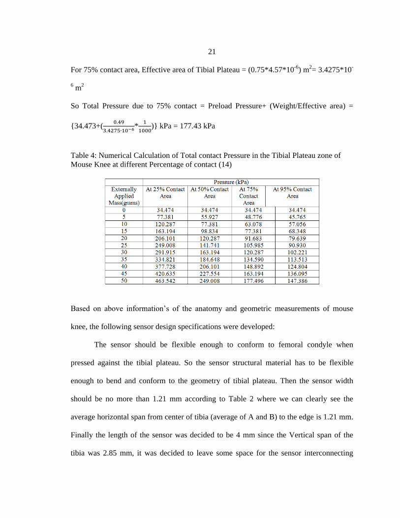
21: Upper and Lower Electrodes Side wirings: All units in mm ...................................... 31
22: High Density wiring part; All units in mm ................................................................. 32
23: Insulation layers with Modified Air Pocket; All units in mm .................................... 32
24: Air Pockets with Connected Air Channels; All units in mm ...................................... 33
25: Pads for All Electrodes; All units in mm .................................................................... 33
26: Design Drawbacks ...................................................................................................... 34
27: Silicon wafer with Primary and Secondary Flat and Orientation;
Image Modified from (5) ............................................................................................ 36
28: Mask Alignment Marks .............................................................................................. 38
29: a) Isotropic wet etching of silicon by KOH results occurs in 54.7
degrees b) Dry anisotropic etching in a plasma or reactive ion
etching environment .................................................................................................... 39
30: Step 1 of the Fabrication process ................................................................................ 40
31: Step 2 of the Fabrication process ................................................................................ 41
32: Step 3 of the Fabrication process ................................................................................ 42

x
LIST OF FIGURES - CONTINUED
Figure Page
33: Step 4 of the Fabrication process ................................................................................ 42
34: Exploded View of the Pressure sensor; Third and Final Iteration .............................. 43
35: Upper and Lower Polymer Layer Final Version; All units in mm ............................. 44
36: Four Upper Electrodes with dimensions in mm unit; b) Sixteen
lower electrodes with Dimensions in mm unit c) Side wiring
distribution of lower electrodes d) both upper and Lower Electrodes
in parallel position....................................................................................................... 45
37: Bump layers for bonding process; All units in mm .................................................... 46
38: created by casting polymer on silicon mold created by etching ................................. 47
39: Bumps layer created around the edge of the sensor .................................................... 48
40: Solid Continuous bump around the edge along with small bumps ............................. 49
41: Exploded view of the final configuration of different layers of the Sensor ............... 50
42: Modified bump Layer with Continuous Solid bumps ................................................ 50
43: Fabrication process outline (20) ................................................................................. 51
44: Optical Exposure system of Mask to wafer: Image redrawn
from textbook (20) ..................................................................................................... 51
45: Illustration of opaque and transparent part of the masks ............................................ 54
46: Electrodes layer Mask with the alignment marks a) wafer view
b) zoomed in view ..................................................................................................... 55
47: Illustration of opaque and transparent zone of the bump layer Mask ......................... 56
48: Layer Mask with the alignment marks a) wafer view b) zoomed in view .................. 57
49: Mask Alignment in progress: a) The bump layer mask is
brought near metal layer mask b) the alignment marks are about
to be overlapped on each other ................................................................................... 57

xi
LIST OF FIGURES - CONTINUED
Figure Page
50: The stress vs. strain curves of PDMS specimens with five different
mixing ratios of the pre-polymer and curing agent (12:1, 16:1, 20:1,
24:1, and 28:1); image modified from (25) ................................................................ 62
51: Stress Vs Strain plot of two different types of PDMS elastomer:
RTV 615 and Sylgard 184; image modified from (22)............................................... 64
52: The exponential curve fit of Thickness Vs frequency of two
PDMS silicone polymer; image modified from (22) .................................................. 65
53: Stress Vs Strain plot of polyimide( containing m-catenatedphenylene
rings) tensile test (29); image modified from (29) ...................................................... 67
54: Stress-strain Diagram of Dupontkapton polyimide from the data
sheet of original manufacturer (31); image modified from (31) ................................. 67
55: Change of Capacitance in a Parallel Plate capacitor ................................................... 69
56: Plot of Sensitivity Vs Applied Pressure; Material PDMS .......................................... 74
57: Plot of Sensitivity Vs Applied Pressure; Material Polyimide..................................... 74
58: of Change of Capacitance Vs Change of Gaps; Material PDMS ............................... 75
59: Plot of Change of Capacitance Vs Change of Gaps; Material Polyimide .................. 75
60: Sensitivity Vs Applied Pressure; Material PDMS and Polyimide .............................. 76
61: Change of Capacitance Vs Change of Gap; Material PDMS and Polyimide ............. 76
62: a) Extruded Cut operation of the model in SolidWorks
b) Imported geometry in ANSYSDesign Modeler c) half geometry
with plane of symmetry (red color) ............................................................................ 83
63: Bonded contact between 2 (due to symmetry plane) Upper
Electrodes (blue) and Upper Polymer layer (red) ....................................................... 85
64: Bonded contact between 16 lower Electrodes (blue) and
Lower Polymer layer (red grooves) ............................................................................ 86

xii
LIST OF FIGURES - CONTINUED
Figure Page
65: Bonded contact between thin insulation layer of polymer (Red)
and three faces in the Upper Polymer Layer (Blue) ................................................... 86
66: Bonded contact between thin insulation layer of polymer (Red)
and surfaces of bumps (Blue) ..................................................................................... 86
67: Bonded contact between lower polymer face (red) and bumps layer (blue) .............. 87
68: Frictionless contact pair between lower polymer layer (red)
and tibial support (blue) with pinball region............................................................... 88
69: SOLID186 Element type with homogeneous Structural Solid
Geometry; Image borrowed from ANSYS help documentation .................................. 90
70: Mesh Generation ......................................................................................................... 91
71: Boundary conditions of the analysis; blue shaded zones were the
fixed supports ............................................................................................................ 92
72: Applying Surface Pressure on top of Polymer............................................................ 93
73: Comparison of equivalent stress for same thickness of Gold
and Copper alternatively embedded in PDMS; electrode
thickness 20 microns ................................................................................................... 98
74: Comparison of equivalent stress for same thickness of Gold
and Copper alternatively embedded in PDMS; electrode thickness
20 micron .................................................................................................................... 98
75: Comparison of Maximum shear stress for same thickness of
Gold and Copper alternatively embedded in PDMS; electrode
thickness 20 microns ................................................................................................... 99
76: Comparison of Maximumdeflection (Z-axis) for same thickness
of Gold and Copper alternatively embedded in PDMS; electrode
thickness 20 microns ................................................................................................... 99
77: Comparison of equivalent stress for same thickness of Gold and
Copper alternatively embedded in Polyimide; electrode thickness
20 microns ................................................................................................................. 109

xiii
LIST OF FIGURES - CONTINUED
Figure Page
78: Comparison of Deflection (Z-direction) for same thickness of
Gold and Copper alternatively embedded in Polyimide; electrode
thickness 20 microns ................................................................................................. 110
79: Equivalent Stress in the Polyimide Structure considering Gold
Electrodes of 5 and 20 microns thickness alternatively ............................................ 114
80: Deflection (Z-directional) in the Polyimide Structure considering
Gold Electrodes of 5 and 20 microns thickness alternatively ................................... 114
81: Equivalent Stress in the Polyimide Structure considering Copper
Electrodes of 5 and 20 microns thickness alternatively ............................................ 115
82: Deflection (Z-directional) in the Polyimide Structure considering
Copper Electrodes of 5 and 20 microns thickness alternatively ............................... 115
83: Comparison of Equivalent Stress in the Polyimide Structure
considering both Copper and Gold Electrodes of 5 microns thickness .................... 116
84: A both End fixed beam under uniformly distributed load W ................................... 118
85: Both end Fixed Polyimide beam with surface pressure of 10kPa ............................ 120
86: Location of Maximum Stress at Fixed end and Maximum
downward deflection at 10kPa pressure ................................................................... 120
87: Typical Read-Out Circuit for Capacitive sensor ....................................................... 125
88: Capacitive Row and Column Senor Array with Scanning Circuits
using Multiplexers; Image and Idea inspired from (41) ........................................... 125
89: Equivalent (Von-mises) stress and directional deformation at
any point in the structure at 1 kPa pressure; material PDMS and Gold ................... 135
90: At 1 kPa,Von-mises Stress distribution on Upper and lower
electrodes and location of max stress; material PDMS and Gold ............................. 136
91: At 1 kPa ,Maximum Principal Stress on Upper and lower
electrodes and location of max stress; material PDMS and Gold ............................. 136
xiv
LIST OF FIGURES - CONTINUED
Figure Page
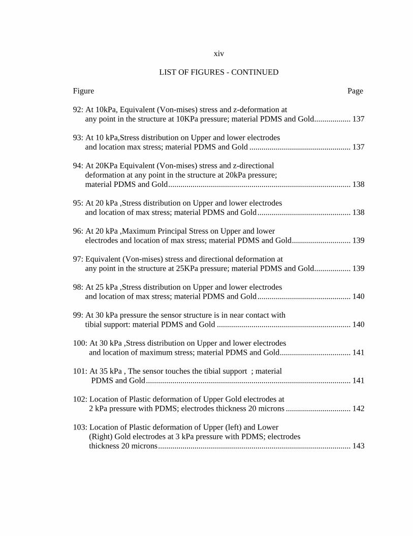
92: At 10kPa, Equivalent (Von-mises) stress and z-deformation at
any point in the structure at 10KPa pressure; material PDMS and Gold .................. 137
93: At 10 kPa,Stress distribution on Upper and lower electrodes
and location max stress; material PDMS and Gold .................................................. 137
94: At 20KPa Equivalent (Von-mises) stress and z-directional
deformation at any point in the structure at 20kPa pressure;
material PDMS and Gold .......................................................................................... 138
95: At 20 kPa ,Stress distribution on Upper and lower electrodes
and location of max stress; material PDMS and Gold .............................................. 138
96: At 20 kPa ,Maximum Principal Stress on Upper and lower
electrodes and location of max stress; material PDMS and Gold ............................. 139
97: Equivalent (Von-mises) stress and directional deformation at
any point in the structure at 25KPa pressure; material PDMS and Gold .................. 139
98: At 25 kPa ,Stress distribution on Upper and lower electrodes
and location of max stress; material PDMS and Gold .............................................. 140
99: At 30 kPa pressure the sensor structure is in near contact with
tibial support: material PDMS and Gold .................................................................. 140
100: At 30 kPa ,Stress distribution on Upper and lower electrodes
and location of maximum stress; material PDMS and Gold ................................... 141
101: At 35 kPa , The sensor touches the tibial support ; material
PDMS and Gold ..................................................................................................... 141
102: Location of Plastic deformation of Upper Gold electrodes at
2 kPa pressure with PDMS; electrodes thickness 20 microns ................................ 142
103: Location of Plastic deformation of Upper (left) and Lower
(Right) Gold electrodes at 3 kPa pressure with PDMS; electrodes
thickness 20 microns ............................................................................................... 143
xv
LIST OF FIGURES - CONTINUED
Figure Page
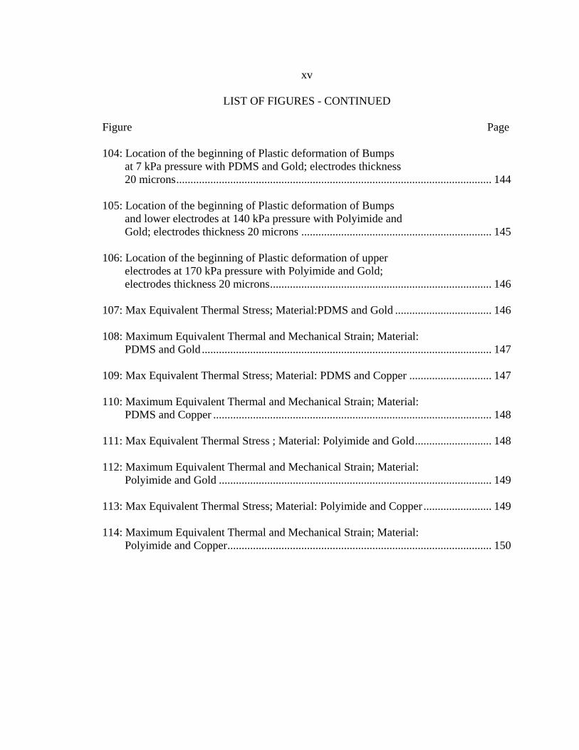
104: Location of the beginning of Plastic deformation of Bumps
at 7 kPa pressure with PDMS and Gold; electrodes thickness
20 microns ............................................................................................................... 144
105: Location of the beginning of Plastic deformation of Bumps
and lower electrodes at 140 kPa pressure with Polyimide and
Gold; electrodes thickness 20 microns ................................................................... 145
106: Location of the beginning of Plastic deformation of upper
electrodes at 170 kPa pressure with Polyimide and Gold;
electrodes thickness 20 microns .............................................................................. 146
107: Max Equivalent Thermal Stress; Material:PDMS and Gold .................................. 146
108: Maximum Equivalent Thermal and Mechanical Strain; Material:
PDMS and Gold ...................................................................................................... 147
109: Max Equivalent Thermal Stress; Material: PDMS and Copper ............................. 147
110: Maximum Equivalent Thermal and Mechanical Strain; Material:
PDMS and Copper .................................................................................................. 148
111: Max Equivalent Thermal Stress ; Material: Polyimide and Gold ........................... 148
112: Maximum Equivalent Thermal and Mechanical Strain; Material:
Polyimide and Gold ................................................................................................ 149
113: Max Equivalent Thermal Stress; Material: Polyimide and Copper ........................ 149
114: Maximum Equivalent Thermal and Mechanical Strain; Material:
Polyimide and Copper ............................................................................................. 150

xvi
ABSTRACT
Rodents are commonly used in biomedical and biomechanical research because of
their genetic and biological characteristics closely resemble those of humans. Rodents
have similar knee joint structures to human beings, and are commonly used as models for
human osteoarthritis. Biomechanical factors influencing the patterns of pressure
distribution within the joint are very important in the pathogenesis of osteoarthritis at the
knee joints. The pattern of pressure distribution of the femoral condyles of weight bearing
knee joints is therefore of great interest.
A flexible and biocompatible Polymer based Micro-Electromechanical (MEMS)
pressure sensor was designed for this purpose with capacitive sensor array embedded
inside the structure. The sensor structure comprises of a 4x16 arrays of sensors embedded
inside the Polymer structure with air gaps and insulation layers to provide a suitable
dielectric medium to achieve better capacitive sensitivity. A three dimensional model of
the sensor was created using ANSYS Workbench Design Modeler and analyzed with two
different types of polymers and metals as potential structural materials of the sensor.
A suitable clean-room fabrication process was proposed and analyzed for the
sensor and corresponding mask designs were created with a CAD (Computer Aided
Design) program. Residual stresses due to mismatch of thermal coefficient of expansion
were calculated along with proposing a schematic readout circuitry for high gain and
signal to noise ratio and failure analysis of the sensor.

1
INTRODUCTION TO MEMS BASED PRESSURE SENSOR
Mems Pressure Sensor Overview
Micro-electro mechanical systems (MEMS) is the technology of very small
devices which merges at the nano-scale into nano-electromechanical systems (NEMS)
and nanotechnology (1). MEMS are widely used to miniaturize sensitive devices like
pressure transducers, accelerometers, strain gauge etc. for specialized applications. Over
the past few years there has been increased interest in fabricating miniature absolute
pressure transducers using silicon integrated circuit technologies with the expectation that
silicon technology can reduce size, improve performance and minimize cost (1) . Several
types of MEMS sensors have been studied to detect pressure including capacitive,
piezoresistive, resonant and fiber optic (2). Among them capacitive pressure sensors are
one of the most widely studied devices for various types of applications such as
biomedical, automotive and aerospace etc.(2). MEMS capacitive sensors provide high
pressure sensitivity, low noise, low power consumption and low temperature sensitivity
(2). The critical constrains for MEMS capacitive sensors are nonlinearity for large
displacement and the low signal level; therefore a parallel plate structure with small
displacement (within the pressure range of interest) and noise suppression would be an
optimal solution (2) .
There are generally two types of pressure sensors which function mainly on the
principle of mechanical deformation and stresses of thin diaphragms induced by the input
pressure (5). The two types are absolute and gage pressure sensors (5). The absolute

2
pressure (absolute pressure is a summation of gauge pressure and atmospheric pressure)
sensor has an evacuated cavity on one side of the diaphragm and the measured pressure is
the “absolute “value with respect to vacuum as the reference pressure (5). The pressure is
applied on the diaphragm by either back-side or front-side pressurization (5). The sensing
element is usually made of thin silicon die and a cavity is created from one side of the die
by means of a microfabrication process (5). Figure 1 shows the cross section of a typical
pressure sensor diaphragm.
Figure 1: Cross section of a typical sensor Diaphragm and the Dotted line represent un-
deflected state. Image modified from (5)
The shape of the diaphragm is arbitrary but generally takes the form of a square or
circle. For the case of a both end fixed circular plate with small deflections (i.e. less than
half of the diaphragm thickness) the deflection is given by equation found in (6):
Equation 1
Where w,r,a and P are the deflection, radial distance from the center of the
diaphragm, diaphragm radius and applied pressure respectively. D is the flexural rigidity
which is given as in (6):

3
Equation 2
Here E, h and ν are young’s modulus, thickness and Poisson’s ratio of the
diaphragm respectively. From equation 1 we can clearly see that the amount of
deflection is directly proportional to the applied pressure. So in ideal case it is
advantageous to use a pressure system which is linear due to simplicity of the calibration
and measurement (6). The deformation of the diaphragm is later transduced into
electrical signals by different transduction methods and both are later packaged into a
robust casing made of metal, ceramic or polymer with proper passivation layer (5).
Piezoresistive and Capacitive MEMS Pressure Sensor
Certain crystals in nature can generate electric voltage upon deformation due to
applied force and this phenomenon is known as piezoelectric effect (5). Piezoresistance
is defined as the change in electrical resistance with applied stress fields (5). The
discovery of piezoresistivity enabled production of semiconductor based sensors. In this
type of pressure sensors there are piezoresistors mounted on or in a diaphragm (6).
Silicon is one of the widely used piezoresistors in micro sensors and actuators. Doping
the boron to silicon lattice produce p-type silicon crystal and doping with arsenic or
phosphorus results in n-type silicon and both p-type/n-type silicon exhibit excellent
piezoresistive effect (5). The piezoresistors convert the stress induced in the silicon
diaphragm by the externally applied pressure into change in electrical resistance which in
turns converted into voltage output by whetstone bridge circuit (5) shown in Equation 3.
The basic operating principle of this type of sensor is that piezoresistors are

4
deposited or diffused on top of the membrane and the resistors are usually connected to a
whetstone bridge configuration to compensate for temperature effect (7).Those
piezoresistors are essentially miniaturized semiconductor strain gauges which results in
change of electrical resistance induced by mechanically applied pressure (5).
Figure 2 demonstrates a typical piezoresistive pressure sensor assembly where
four piezoresistors (R1, R2, R3 and R4) are implanted beneath the surface of the silicon
die. The resistors R1 and R3 are subjected to a stress field by the applied pressure which
results in an increase of electrical resistance in these resistors (5). On the other hand the
resistors R2 and R4 experience a decrease in their electrical resistance because of their
orientation.
Figure 2: a) Typical Piezoresistive Sensor Assembly b) Wheatstone bridge; Image
modified from (5)
The output voltage Vo and the input voltage Vin to the whetstone bridge are
related by the following equation and the changes of resistance as induced from applied
pressure is measured using the equation found in (5) which is:
Equation 3

5
The main advantage of piezoresistive pressure sensors are the simple fabrication
process, high linearity and the output signal is conveniently available as a voltage (5).
However these sensors have very large temperature sensitivity and drift (5). Because of
the low sensitivity these sensors are not suitable for very low pressure differences (5).
There is another type of micro-pressure sensor that utilizes the change of capacitance
measurements. Two electrodes of thin metal films are deposited on bottom and top of the
diaphragm and parallel to each other (5). Whenever pressure is applied on the diaphragm
the gap between the two electrodes will narrow which leads to change of capacitance
across the electrodes (5). The simplest structure of a capacitive sensor can be described
by two flat parallel plates with area A and distance d as shown in Figure 3
Figure 3: A Parallel plate Capacitor, Image modified from (7)
The capacitance value C in a parallel –plate capacitor can be related with the gap
distance d by the following equation:
Equation 4
Where εr is the relative permittivity of the dielectric medium, ε0 is the permittivity
in the vacuum where ε0= 8.854x (Farad/meter) and A is the overlapping area
between the parallel plates (5). The capacitance value increases with the increase in either
6
effective area A or permittivity of the dielectric medium εr and decreases as the gap
distance increases. Based on the parameters on the above equation a capacitive sensor can
be of 3 types: a) ε-type where the capacitive sensors has a fixed value of A and d but the
dielectric properties are variable; b) D-type where the sensors has a fixed value of A and
ε but the distance is variable and c) A-type where the sensors has a fixed values of d and
ε but the area is variable.Since relative permittivity is not a fundamental variable and
can be temperature dependent, inhomogeneous or anisotropic for certain materials ε-
type sensors are generally not common (7). The D-type capacitive sensors are very
effective for small displacement measurements and most common type of capacitive
micro-pressure sensors usually used. However non-linearity in the measurement might be
caused by fringe fields or parasitic capacitance. The accuracy of A-type sensors highly
depends on the mechanical accuracy, flatness of the electrode surface, obliqueness,
deformation, frayed edges and gaps (12).
Capacitive based sensor mechanisms are inherently less sensitive to the variations
in the operating temperature and very low power consumption can be obtained from these
devices. However the capacitance to be measured is usually very small range so an
effective readout circuit interface needs to be constructed which can be either integrated
in the sensor die or at least to be positioned very close to the sensor chip (7).
Motivation
Osteoarthritis (OA) also known as degenerative arthritis is a group of mechanical
abnormalities involving degradation of joints including articular cartilage, limited

7
intraarticular inflammation with synovitis and subchondral bone (3). Some of the Major
symptoms of this disease are joint pain, stiffness, functional impairment, loss of mobility
and sometimes inflammation (3). A variety of other causes like developmental,
hereditary, metabolic disorders and mechanical deficits may initiate processes leading to
loss of cartilage. The integrity and quality of cartilage cell covering the knee joint plays
an important role in the development of Osteoarthritis.
Figure 4 : Schematic diagram of the knee joint showing synovial joint tissues affected by
OA; image modified from (8)
Biomechanical factors that influence the patterns of pressure distribution within
the joint are very important in the pathogenesis of Osteoarthritis. There are two
fundamental mechanisms that are related to the risk factors for development of OA which
are adverse effects of “abnormal” loading on normal cartilage or of “normal” loading on

8
abnormal cartilage (3). One of the main reasons that contribute to the “abnormal” state of
articular cartilage is “Aging”. Those persons who are vulnerable to development of OA,
some local mechanical factors such as abnormal joint congruity, joint misalignment,
muscle weakness, meniscal damage, ligament rupture etc. can aggravate the possibility of
OA progression (8). Also genetic factors can cause disruption of chondrocyte and
influence the composition and structure of the cartilage leading to abnormal
biomechanics (3). Conditions that produce increased load transfer and/or altered patterns
of load distribution can enhance the initiation and progression of OA (3).
Articular cartilage is subjected to a range of static and dynamic mechanical
loading in human knee joints (9). The ability of cartilage to withstand these different
types of compressive, tensile and shear loads depends on the composition and structural
integrity of its extracellular matrix (ECM) (9). Articular cartilage provides lubrication
and load bearing functionality during motion of synovial joints (9). Mechanical stresses
play an important role in the pathogenesis and progression of Osteoarthritis (10).
Structural failure due to mechanical stresses in OA can involve all tissues of the joint,
including the capsule, synovial membrane and subchondral bone, ligaments,
fibrocartilaginous menisci in joints such as knee and the articular cartilage (10).
Abnormal mechanical stress can cause the structural failure of articular cartilage
in OA, damaging initially normal tissues from the failure of pathologically impaired
articular cartilage (10). Articular cartilage injuries might occur due to either traumatic
mechanical destruction or progressive mechanical degeneration. As the loss of articular
cartilage lining continues the bone underneath becomes unprotected from mechanical

9
wear and tear and begins to break down which will eventually lead to osteoarthritis. The
pattern of contact pressure distribution of the weight bearing knee joints therefore is of
great interest.
Osteoarthritis and Contact Pressure
Recent studies have found that contact stress is a potential indicator of subsequent
symptomatic osteoarthritis development in the knee joint. The results of the study in (11)
indicated that higher tibiofemoral contact stress increased the risk of both worsening of
cartilage morphology and BMLs (Bone marrow lesions). These studies were consistent
with the hypothesis that excessive loading within tibiofemoral joint compartments
longitudinally contributes to pathology articular cartilage and subchondral bone (11). It
was evident from the studies done in (11) that contact stress estimation can predict the
mechanical degradation of a knee whether it is a normal or Osteoarthritis affected knee.
Contact stress has previously been shown to be efficient and accurate means of predicting
the risk of development of incident symptomatic knee Osteoarthritis which may also be
useful for predicting anatomic degradation (11).
Estimation of contact pressure may also guide development of specific therapies
to positively change the direction of knee OA and guide decisions regarding which
patients might benefit from surgery or prescribing a surgical or non surgical therapy
therefore planning to optimize reduction of contact stress (11).

10
Role of Knee Loading in Osteoarthritis
Joint alignment influences to the distribution of load on the articular cartilage and
other tissues of weight bearing joints. The external knee adduction moment is generated
while walking and this moment pushes the knee into the varus which results in a
compression of the medial joint compartment (10). It has been found that the magnitude
of the baseline adduction moment is a good indicator of progression of medial
compartment knee osteoarthritis (10).
In order to understand knee contact pressure mechanism and its relation to
osteoarthritis we need to study the interior of the knee joints. The anatomy of the knee
describes as it has 3 bones which are Tibia, femur and patella as shown in Figure 4. There
are three compartments which are medial, lateral and patellofemoral (Figure 3) and four
ligaments which are MCL, LCL, ACL and PCL (Medial, lateral, anterior and posterior
cruciate ligaments). Also there are 2 menisci and articular cartilages as shown in (Figure
4).
For knee osteoarthritis the most relevant and widely studied load is the external
knee adduction moment generated by ground reaction force vector passing medial to the
joint center as shown in Figure 5. This adduction moment forces the knee laterally into
varus (When a knee is perfectly aligned it has its load bearing axis on particular line that
goes through middle of the leg, hip, knee and ankle, but when the knee is not aligned
perfectly it is known as varus (bow legged) or valgus alignment (knock-kneed)) resulting

11
Figure 5: a) Ground Reaction force vector (GRF) which is at a distance from rotation
center of the knee joint producing an external adduction moment of force with knee co-
ordinate system (Medial view of Right knee) where The x-, y-, and z-axes correspond to
the tibial rotation, flexion extension, and varus-valgus axes, respectively; image modified
from (15)
in compression of the medial joint compartment causing the stretching of the lateral
structure (10). The adduction moment has a great influence on the load distribution
between medial and lateral plateau (10). The higher the adduction moment the greater the
load on the medial plateau relative to the lateral plateau and adduction moment is higher
in knee with osteoarthritis than in a normal knee (10).
Knee adduction moment could be measured during gait with laboratory based
measurement system or laboratory free settings like Ambulatory movement analysis
systems including instrumented force shoes (IFS), inertial and magnetic measurement
systems (IMMS) etc.(43)The mechanical alignment of the lower limb plays a vital role in
the distribution of load across the medial and lateral knee joint compartments. Sometimes
there could be preexisting mal-alignment that can contribute to the development of OA or
the mal-alignment could be a result of osteoarthritis process due to cartilage loss, bonny

12
attrition and meniscal damage (10). In a neutral knee position the ground reaction force
vector shown in Figure 5 slightly passes medial to the knee joint center (10). In a varus
position the ground force vector is medially more displaced to the knee joint center
thereby increases the knee adduction moment and compressive load across the medial
compartment (10). In a valgus knee the ground reaction force vector passes more laterally
with increasing valgus thereby increasing the load across the lateral compartment (10).
Varus mal-alignment is common in people with medial tibiofemoral joint OA (10).
Table 1: Comparison of Contact stress between control knees and Symptomatic OA case
Knees found in (4)
In Summary the development of tibiofemoral OA is strongly influenced by
contact geometry and loading factors that can alter the cartilage microstructure and
vitality. The combination of mal-alignment and altered anatomy are most likely
responsible for higher contact stress in the knees which in turn leads to OA (4).

13
Identifying the maximum contact stresses and distribution between a tibiofemoral OA
case and control knees are extremely important for the prediction of incident and
progressive knee OA. Contact stress is a stronger predictor of OA than demographic or
anthropometric measures which is evident from the above Table 1.
Mouse as Experiment Model
Animal modeling of Osteoarthritis is performed inorder to controllably reproduce
the scale and progression of joint damage so that opportunities to detect and modulate
symptoms and disease progression can be identified and new therapies be developed (12).
An ideal animal model is the one with relatively low cost and exhibits reproducible
disease progression with a magnitude of effect large enough to detect differences within a
short period of time and replicate human OA (12).
Although risk factors of OA were identified by various epidemiologic studies
limited to age, trauma history, occupation and gender, large contributing casue of OA is
accumulated mechanical stress (13). Due to rapid progress of mouse genomics and the
availability of transgenic and knockout mice it is the most ideal animal model to study
osteoarthritis progression and development by producing instability of joints through
surgical intervention (13). These genetically modified transgenic knockout mouse will
develop premature cartilage degeneration to observe the effect and prognosis of OA (14).
Surgically induced models are used where the meniscus of the specimen is removed
which will allow mechanical wear and degradation of the cartilage within the knee (14).
These knockout mice have permitted the validation of many mechanisms associated with
risk factors of OA such as biomechanical instability, injury, inflammation etc. These

14
mouse models will develop spontaneous or accelerated OA due to altered biomechanics
which might not have been possible with human as test subjects from research
perspective (15).
The pressure sensor for this report was designed based on the mouse dissection
data received in courtesy of the author of the work in (14). It was intended to be used for
measuring contact stress distribution in the tibiofemoral joint of mouse knee in order to
distinguish between a control knee cartilage contact stresses with a degenerated cartilage.
Thus mouse was an ideal model to perform osteoarthritis quantification as a disease in
the laboratory environment.

15
DESIGN AND MODELING
Array Configuration
Capacitors can be built in various ways with MEMS technologies. A distributed
array of capacitors in rows and columns of a matrix configuration was chosen in order to
map the pressure distribution inside knee joint. Each intersection of rows and columns
constructed from conductive strips of metal layers known as Electrodes were separated
by a suitable elastic dielectric medium and forms a single cell of coupling capacitor or a
unit sensor. These unit cells are the core sensing elements of the pressure sensor and the
higher the spatial density of the cells the higher the spatial resolution of the total sensor
will be.
Figure 6: Row and Column configuration
The unit cell is analogous to the ‘Pixel’ of an electronic display monitor where
higher pixels usually results in sharper and smoother images on the screen. Figure 6
displays a grid structure of rows and columns of electrodes and each intersection have
formed a coupling capacitance between the electrodes. When the dielectric layer between
16
the electrodes is squeezed due to pressure being exerted on the corresponding area of the
sensor the capacitance between the two overlapping area will change.
The sensor was designed based on an array configuration and it consisted of high
density capacitive cells in a grid format that will enable us to map the distribution of the
pressure inside the knee joints. The distribution will be based on location wise output
from each unit cell. The location of the output (capacitance or voltage change) can be
traced from relative position of column and row intersection when the scanning circuit
will scan the columns and rows sequentially. The values of the change of capacitance will
be inserted in a computer programming code to construct a matrix whose dimension will
be same as the sensor grid configuration. From there intensity of the pressure can be
easily distinguished based on location to form a complete pressure map of the desired
area.
Some previous works that were based on capacitive pressure sensor array could
be mentioned in this regard. Hyung-Kew, Sun-Il et al. 2006(16) worked on a fexible
polymer based tactile sensor which utilized a total of 16x16 of cell array made of copper
electrodes embedded in PDMS (Polydimethylsiloxane) with a spatial resolution of 1mm
and utlized the theory of capacitance change between the copper elctrodes separated by
12 microns gap (6 microns by a spacer creating air gaps in the middle and 6 microns by
insulation layer)with an initial capacitance of a single cell being 171 femtoFarad. Their
cell size and electrode size were 600 x 600 µm2 and 400 x 400 µm2 respecively.

17
Figure 7: Work of Hyung-Kew, Sun-II et al. (16) a) The 16 x 16 arrays of capacitive cells
b) Flexibility of the sensor structure due to PDMS; Photo modified from reference (16)
Figure 8: Work of Dagamseh, Wiegerink et al. (17); 128 SU-8 hairs on top of array of
parallel plate capacitors; Photo modified from reference (17)
Dagamseh, Wiegerink et al. 2012(17) created an artificial hair sensor arrays for
flow pattern observation. Their sensor was based on the capacitance changes between
two electrodes deposited on top of a silicon Nitride membrane and a common underlying
electrode which was the silicon substrate and implanted SU-8 hairs on top of the
membrane. They used two aluminum electrodes with the SU-8 hair in the middle as
upper electrodes and a conductive silicon substrate with deposited silicon nitride as
bottom electrode separated by 600 nm poly-silicon which defined the capacitors gap.
They connected 124 parallel hairs in this way and formed the array of capacitive sensors.

18
Figure 9: Work of Cheng, Huang et al. 2009 (18), capacitive sensor arrays a) Both
sensing electrodes at the bottom b) The floating electrodes with no interconnections act
as top electrodes
Another impressive implementation of capacitive type sensor arrays were
demonstrated by the work in (18). They fabricated a tactile sensor where the sensing row
and column electrodes made of copper (30 microns) were printed on a flexible printed
circuit board (FPCB) with the interconnects being printed on either side of the FPCB
having 100 microns thickness and the floating gold electrodes of 0.16 microns thickness
were patterned in to PDMS along with chromium as the bonding substance. They
improvised a solution to reduce the parasitic capacitance due to overlapping between the
row and column interconnects since the row and column interconnects were printed on
either side of the FPCB. In this way they were also able to avoid long and thin metal
interconnects which are usually vulnerable to bending. Their flexible tactile sensor
consisted of 8 x 8 arrays of sensing elements.

19
Pressure Sensor for Rodents: Initial Design
This pressure sensor was primarily designed to measure pressure intensity and
mapping of pressure distribution inside tibia-femoral interaction of a mouse knee joint.
The design was based on various dissection data on laboratory mouse (14).
Figure 10: The Anatomy of Knee joint and view of Tibial Plateau; Image modified from
Reference (19)
The average data received from experiment of various mouse dissections from (14) are
tabulated below:
Table 2: Experimental Measurements of Tibial Plateau area of Mouse Knee (14)

20
The Femoral condyles are going to interact with Tibial Plateau during various angles of
Knee movements. So the geometric measurements of Femoral Condyle area were also
included in Table 3.
Table 3: Experimental Measurements of Condyles area of Mouse Knee (14)
The anterior and posterior cruciate ligaments restrict movement of tibia and femur
from sliding backward over each other and the lateral and medial ligaments prevents the
femur from sliding side to side as well as lateral joint bending.
To perform loading on the mouse knee, the author in (26) fabricated a special type
of loading apparatus where a single mouse leg could be mounted and external force could
be applied along tibial axis to the femur. Based on experimental calculation of tibial area,
percentage of tibiofemoral contact area, amount of preload from the loading apparatus
and ranges of externally applied load the pressure range of our desired pressure sensor
was established.
Here is a sample calculation of pressure in the tibiofemoral contact zone based on
the above information:
From Table 2, Total area of Tibial Plateau = 4.57 mm2= 4.57x10⁻⁶m
2
For externally applied mass of 50 gram, weight=
Kg* 9.8
= 0.49 Newton
Preload Pressure from the Loading apparatus= 34.473 kPa
21
For 75% contact area, Effective area of Tibial Plateau = (0.75*4.57*10-6
) m2= 3.4275*10
-
6 m
2
So Total Pressure due to 75% contact = Preload Pressure+ (Weight/Effective area) =
{34.473+(
*
)} kPa = 177.43 kPa
Table 4: Numerical Calculation of Total contact Pressure in the Tibial Plateau zone of
Mouse Knee at different Percentage of contact (14)
Based on above information’s of the anatomy and geometric measurements of mouse
knee, the following sensor design specifications were developed:
The sensor should be flexible enough to conform to femoral condyle when
pressed against the tibial plateau. So the sensor structural material has to be flexible
enough to bend and conform to the geometry of tibial plateau. Then the sensor width
should be no more than 1.21 mm according to Table 2 where we can clearly see the
average horizontal span from center of tibia (average of A and B) to the edge is 1.21 mm.
Finally the length of the sensor was decided to be 4 mm since the Vertical span of the
tibia was 2.85 mm, it was decided to leave some space for the sensor interconnecting

22
terminals and for the convenience of routing the wires to the end of the sensor. The
sensor was designed to measure pressure distribution in either lateral or medial side of
Tibial plateau so this single sensor will work on both ‘A’ or ‘B’ region (Figure 10)
equally.
The working principle of the sensor was to measure the capacitive change to
estimate the applied pressure. When there will be no pressure on the sensor the
capacitance read out the sensor should be zero. When a pressure will be applied the
distance of the dielectric layer would be reduced and the capacitance among the sensing
electrodes will increase. Our pressure sensor design consisted of an upper polymer layer,
upper electrodes embedded inside the upper polymer layer, an insulation layer, a lower
polymer layer and lower electrodes embedded inside the lower polymer layer in general.
There have been some chronological improvements and changes that were made in the
sensor design based on the experimental data received from further mouse dissection
results. The sensor dimensions and configurations were modified time to time according
to the feedback received from the lab experimental data of mouse dissections performed
by the author of the work in (14).
There were several trial designs of the pressure sensor during the ongoing effort
to make a contact stress distribution measuring sensor for rodents. Each trial was later
adjusted carefully considering structural point of view as well as possible complexity of
readout circuitry, interconnectivity and ease of data acquisition from the sensor. Several
design changes were made to the sensor following the above approach. The final trial was
considered to be eligible to be fabricated as a prototype sensor but the implementation

23
was depended on the decision of proper material selection. In this thesis an effort was
also made for comparative material analysis of the sensor both from structural and
sensing material perspective so that an optimum material could be recommended before
moving onto actual fabrication of the sensor. A generalized micro-fabrication protocol
and mask designs based on those fabrication steps were recommended at the later chapter
of this work.
The following trial designs of the sensor were able to finally recommend and
establish an optimum dimension suitable to be used inside the knee joint. Description and
changes of each trial is given below:
First Iteration of Design
Figure 11: Exploded View of the different layers of the very first trial design of the
Pressure sensor

24
Upper and Lower Polymer Layer
Figure 12: Upper and Lower Polymer Layer of the sensor, Units in ‘mm’
The two identical upper and lower polymer structures constituted the total sensor
which encapsulated the metal electrodes inside the structure. The polymer structure
would also ensure the required flexibility of the sensor as well as structural rigidity. The
width of the polymer layer would define the total width of the sensor, which was
estimated to be 1.72 mm according to the preliminary studies (14) who was working on
the dissection of the mouse knees. Later it was found that the width that was initially
estimated was not convenient enough for the insertion of the sensor inside the knee joint
and readjusted later. The initial thickness of the upper and lower polymer layers were
decided to be 0.24mm each.
Upper Electrodes
Figure 13: Upper Electrodes with dimensions; all units in mm

25
The sensor was designed based on an array of parallel plate capacitors running
vertically and horizontally in two parallel planes but separated by a dielectric medium .
There were 4 upper electrodes that would be electroplated in the silicon wafer and then
polymer material would be casted on top of the electroplated electrodes with a sacrificial
coating that will act as bonding and adhesive material between the polymer and the
metals so that when the polymer was being peeled from the silicon wafer, the metal
electrodes would still adhere with the polymer surface. Each upper electrode extended
vertically straight downward to the sensing area and after the sensing area the
interconnecting metal wires extended with longer aspect ratio with metal pads at the end
having larger width to accommodate wire bonding/soldering electrical wires to be
connected with the readout circuit later as shown in Figure 14. The dimension of each
square plate was 200x200 microns and the pitch between each vertical electrode was 250
microns with 50 microns air gap both vertically and horizontally.
Figure 14: Interconnecting wires for Upper Electrodes; Dimensions in mm unit

26
Lower Electrodes
Figure 15: Lower electrodes with interconnecting wires sideways; all units in mm
The initial design contained 16 horizontal electrodes embedded in the lower
polymer layer and the metal deposition process was similar to upper electrodes
mentioned above by electroplating process. This array of lower electrodes produced high
density metal traces with minimum trace size of 20 microns with 20 microns air gap
between the high density interconnecting wires. The interconnecting wires were designed
to be routed from any one side of the sensor since that area of the sensor will be buried
under the gap between A and B region (Figure: 10) where least contact between tibial
plateau and femoral condyles would occur.
Due to space limitation of 1.72 mm width the routing of the interconnecting
terminals were very closely populated within spatial constraints. The square electrodes
had exactly the same dimension as the upper electrodes and the projection of the area
were similar. The actual sensing area was 3.95 mm for both upper and lower electrodes
and their overlapping state looked like the same as shown in figure 10 which constituted
the actually sensing area of the sensor.

27
Thin Insulation Layer With Air Pocket
A thin insulation layer was designed to be placed in between the upper and lower
electrodes which would provide a better dielectric coefficient (A composite dielectric
medium of air and polymer) and prevent the electrodes coming into direct physical
contact with each other. The insulation layer had a total thickness of 12 microns and it
contained a 6 microns air pocket inside the structure as shown in Figure 16 and 17.
Figure 16: Insulation layer with a single Air Pocket; All units in mm
Figure 17: thin insulation polymer layer containing air pocket, zoomed out view; Units in
mm

28
The 16 X 5 arrays of cells required 80 corresponding air pockets to be created
inside the thin insulation layer of polymer. Due to gap provided by this insulation layer,
electric charge will build up in the parallel plates between their projected overlapped area
once a source voltage will be applied to any one row or column of electrodes.
Finally the view of upper and lower electrodes sandwiching the insulation layer with air
pocket is demonstrated in Figure 18 below:
Figure 18: Upper and lower electrodes floating over insulation layer
The preliminary thickness of the upper electrodes, lower electrodes, insulation
layer and the two identical polymer layers were designed as 1 micron, 1 micron, 12
microns with 6 microns air gap and 240 microns respectively. But later we adjusted our
design in response to finite element analysis along with parallel plate capacitance
equations to achieve an optimum thickness of the metal layers, proper polymer material
selection and total thickness of the sensor as well.
Second Iteration of Design
The next design changes were solely based on the fabrication steps that were
decided for the fabrication of the pressure sensor. The circuit connectivity would require

29
more space compared to the previous design and ease of handling was another priority .
The sensor dimensions were adjusted once again and a tentative final estimation was
reached based on the laboratory experimental data of dissection of mouse knee’s courtesy
of the author in (26). The optimum dimension of the sensor part was decided to be 1.2 X
4 mm width and length respectively. Any sensor dimension beyond 1.2mm would not fit
within the tibiofemoral interaction zone and the rest of the dimensions outside the knee
joint interaction were flexible to choose. To allow this change of width, the total number
of vertical electrodes were reduced from five to four and total number of effective
capacitive cells were reduced from 80 (5X16) to 64 (4X16) in the second iteration of
design. The other changes that were made in the sensor structure were the insulation layer
containing the air pockets described later in this chapter.
Full Sensor
Figure 19: Full sensor design changes; All units in mm

30
The final optimum dimension of the sensor area containing the capacitive cells
were determined to be 1.2 mm by 4 mm as shown in the Figure 19 and it was introduced
since second iteration of design changes of the sensor. The dimensions were once again
set on the basis of previous experimental mouse dissections results received courtesy of
the author in (14). It was realized that the sensor electrical circuit connectivity would
demand more space which would result in ease of handling, calibration and data
collection after the completion of the sensor. As a result the lower part outside the
original capacitive sensing area was determined to be 30 mm by 60mm polymer structure
to house all metal wirings and connecting pads. The ratio of the length and width of the
sensor outside knee joint to inside knee joint (main sensor part) was approximately 10:1
and 50:1 respectively.
Upper and Lower Polymer Layer
Figure 20: Original Area of the sensor; All units in mm
As shown in Figure 20, the new optimum dimension of the sensor was determined
to be 1.2 mm by 4 mm since the new width would allow to provide more space for
routing the side wirings of the lower electrodes as well as fit inside the knee joint more
conveniently.
31
Upper and Lower Electrodes
Figure 21: Upper and Lower Electrodes Side wirings: All units in mm
Dimensions of the Upper and lower electrodes, air gaps and pitch were kept
exactly the same as first design except the dimensions of the side wirings and the wirings
projecting from the vertical electrodes. As shown in Figure 21 and 22, the trace size in
the high density side wirings of the horizontal electrodes were 8.75 microns and air gap
between the side wirings were 5 microns. For vertically running upper electrodes the size
of the wires was easier to solve since only four extended wires need to be accommodated
in this regard. The wirings non-uniformly extended at the end of the sensor (4mm) and
projected into a larger geometry with gradual increment in width of the wirings shown in
Figure 21. The width of the vertical wires started with 70 microns within knee joint and
extended to a final width of 1mm (1000 microns) outside of the knee joint. The initial
width ratio of horizontal side wires to vertical wires was 1:8 and final width ratio was

32
1:1. Both upper and lower electrodes were parallel to each other as before and lay in two
parallel planes with 12 microns gap between them.
Figure 22: High Density wiring part; All units in mm
Insulation Layer
Figure 23: Insulation layers with Modified Air Pocket; All units in mm
33
Figure 24: Air Pockets with Connected Air Channels; All units in mm
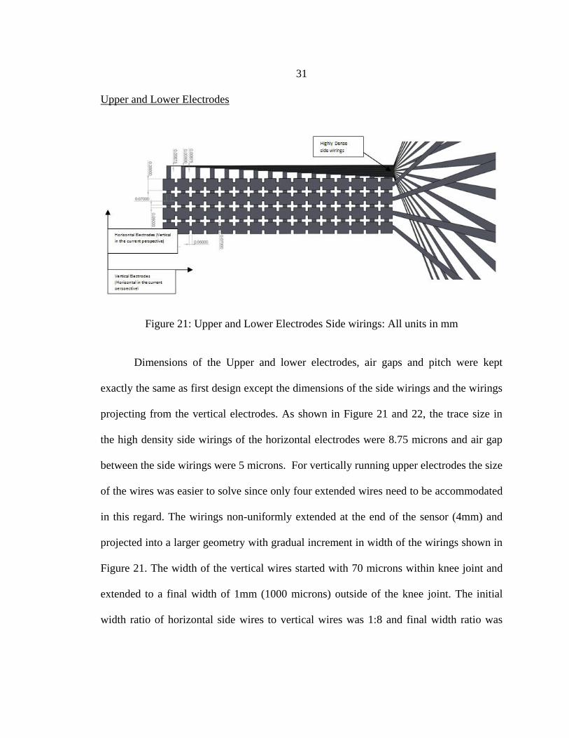
Due to reduction of one vertical electrode, the size of each air pockets were
adjusted to a new dimension of 225X225 microns with horizontal gap of 25 microns and
vertical gap of 20 microns shown in Figure 23. This time the air pockets were not isolated
but connected by tiny air channels of 20 microns width with each other and the entire air
channel finally opens to atmosphere at one end shown in Figure 24. As a result of these
micro-fluidic channels, when the insulation layer would be deformed under pressure, the
trapped air would be able to pass through these channels towards open atmosphere and
the pressure inside the sensor would initially remain atmospheric before deformation
starts.
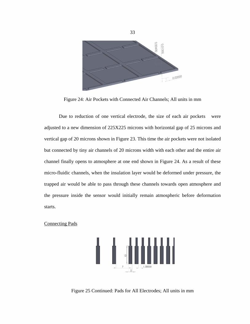
Connecting Pads
Figure 25 Continued: Pads for All Electrodes; All units in mm

34
One of the primary aspects of this second iteration of design for this sensor was,
the features were made as big as possible especially the part located outside the knee joint
and not so much space were left in the first design of the sensor compare to second
design. To be consistent with those criteria the sensor lower part was designed with larger
surface area to be accommodated in a single 100mm silicon wafer easily. Based on this
design it would be possible to fabricate a single sensor at a time over a 100mm silicon
wafer in the clean-room environment. The terminal pads of both 16 horizontal and 4
vertical electrodes were kept at 2mm width and 10 mm length. The air gap between
terminal pads of the vertical and horizontal electrodes were 7 mm and 1.5 mm
respectively as shown in Figure 25.
Drawbacks of This Design
Figure 26: Design Drawbacks

35
One of the major Drawbacks of the second iteration of the design for this pressure
sensor was overlapped wires for both Vertical and Horizontal electrodes in multiple
locations. As a result of overlapping there could be parasitic capacitance growing among
wires and connecting terminals which would be counted as gain and offset errors that
cannot be suppressed by auto calibration (7). Also because of the asymmetric distribution
of the side wires of the horizontal electrodes all 16 wires were routed in the same
direction which resulted in a high density metalized features of very small size. Since
they were not overlapping and all the 16 side wirings would be in same potential so there
were less chances of developing parasitic capacitance among the high density metal parts.
But asymmetric nature of the design could produce too much stress concentration in one
side of the sensor thereby leading to failure of the delicate metal layers. Also to
accommodate the big dimensions of the lower part of the sensor, only one sensor could
be fabricated on a wafer size of 100mm diameter which would not be so efficient and
cost effective considering the expensive nature of such clean-room micro fabrication.
These shortcomings were attempted to overcome in the third and final iteration of the
design.
Third Iteration of Design: Micro-Fabrication Steps
The Next iteration of the design parameters such as sensor width, number of
electrodes, thickness of metal layers, and total width of the sensor was modified
according to initial clean room micro- fabrication process steps. The sensor was designed
to be fabricated on a standard cleanroom environment over a silicon wafer following

36
micro-fabrication and photo-lithography techniques. A short description of different
Micro-fabrication terminologies before describing the sensor Micro-Fabrication steps is
given below:
Photolithography
Photolithography is one of the most significant steps in Micro-fabrication where
patterns are created in substrates with sub micrometer resolutions (5). It encapsulates all
the steps involved in transferring a pattern from a mask to the surface of the silicon wafer
(20). The basic steps in Photolithographic process are discussed below:
Cleaning Wafer
Figure 27: Silicon wafer with Primary and Secondary Flat and Orientation; Image
Modified from (5)
Micro-fabrication starts with n- or p- type silicon wafers with 1 to 8 inch
diameters are being widely used in the IC fabrication industry. They are indentified by a
standard straight edge known as wafer flats in their geometry. The wafer flats indicate the
wafer type (n-type or p-type) and the surface orientation (<100> or <111>) as shown in

37
the Figure 27. The cleaning of the wafer is mostly done by deionized water (DI) and a
solution of hydrofluoric acid removes any oxide that may have formed in the wafer
surface (20).
Barrier Layer Deposition
After the wafer is cleaned it will be covered with some barrier layer that will
either provide insulation or act as a etch mask during photo lithography. Some common
barrier layers are Silicon Dioxide, Silicon Nitride, Polysilicon, photoresists and metals
etc. The processes that are used to deposit these barrier layers are chemical vapor
deposition, physical vapor deposition, thermal oxidation, sputtering and vacuum
evaporation etc. (20)
Photoresists Layer
Once the barrier layers have been formed the silicon wafer is coated with some
light sensitive material known as photoresist. The wafer surface needs to be cleaned to
ensure good adhesion between the photoresist and surface. Photoresists are typically
applied over silicon wafer in liquid form by spin coating the wafer on a chuck at 1000-
5000 rpm resulting in 2.5 to 0.5 microns thickness respectively. The actual thickness of
the resist depends on its viscosity and is inversely proportional to the square root of the
speed. (20)

38
Soft Baking
This is a drying step used to improve adhesion and remove any solvent from the
photoresist and usually done from 5-30 minutes in an oven from 60 to 1000C in air or
nitrogen atmosphere following manufacturer specifications closely (20).
Alignment of Mask
Mask alignment is used to transfer any pattern to the wafer sequentially in case
multiple patterns are present. For that purpose special alignment marks are used in the
mask design to keep track of the reference point and orientation. Mask alignment could
be controlled by computer or manually depending on the accuracy requirement of the
alignment tolerances. The basic manual alignment equipment uses an adjustable x-y stage
to move into the position below mask and the mask is spaced 25 to 125 µm above the
wafer surface (20). The Figure 28 shows alignment marks in a mask design.
Figure 28: Mask Alignment Marks
Photoresist Development
After the mask alignment is done the photoresist is exposed to high intensity
ultraviolet light (20). Wherever the resist comes into contact with UV light that part of
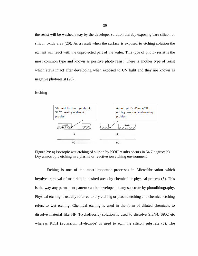
39
the resist will be washed away by the developer solution thereby exposing bare silicon or
silicon oxide area (20). As a result when the surface is exposed to etching solution the
etchant will react with the unprotected part of the wafer. This type of photo- resist is the
most common type and known as positive photo resist. There is another type of resist
which stays intact after developing when exposed to UV light and they are known as
negative photoresist (20).
Etching
Figure 29: a) Isotropic wet etching of silicon by KOH results occurs in 54.7 degrees b)
Dry anisotropic etching in a plasma or reactive ion etching environment
Etching is one of the most important processes in Microfabrication which
involves removal of materials in desired areas by chemical or physical process (5). This
is the way any permanent pattern can be developed at any substrate by photolithography.
Physical etching is usually referred to dry etching or plasma etching and chemical etching
refers to wet etching. Chemical etching is used in the form of diluted chemicals to
dissolve material like HF (Hydrofluoric) solution is used to dissolve Si3N4, SiO2 etc
whereas KOH (Potassium Hydroxide) is used to etch the silicon substrate (5). The

40
etching rate depends on the concentration of the etching solution, type of the material to
be etched and temperature of the solution. Dry etching is suitable to achieve highly
anisotropic profile like avoiding undercutting problem involved in wet processes shown
in Figure 29. Plasma dry etching system uses a stream of positive charge carrying ions of
a substance with large number of electrons diluted by inert carrier gas like argon, and it
can be generated by high voltage electric charge or RF in vacuum (5). Reactive ion
etching (RIE) is a combination of plasma and sputter etching processes where plasma
systems are used to ionize reactive gases and the surface is bombarded by the accelerated
ions. Both Plasma and RIE etching results in highly anisotropic etching process whereas
chemical etching results in isotropic etching (5).
Recommended Fabrication Steps
Figure 30: Step 1 of the Fabrication process
Step 1. a) Silicon Nitride (Si3N4) passivation layer would be used to act as
barrier layer or etch Mask shown in Figure 30.
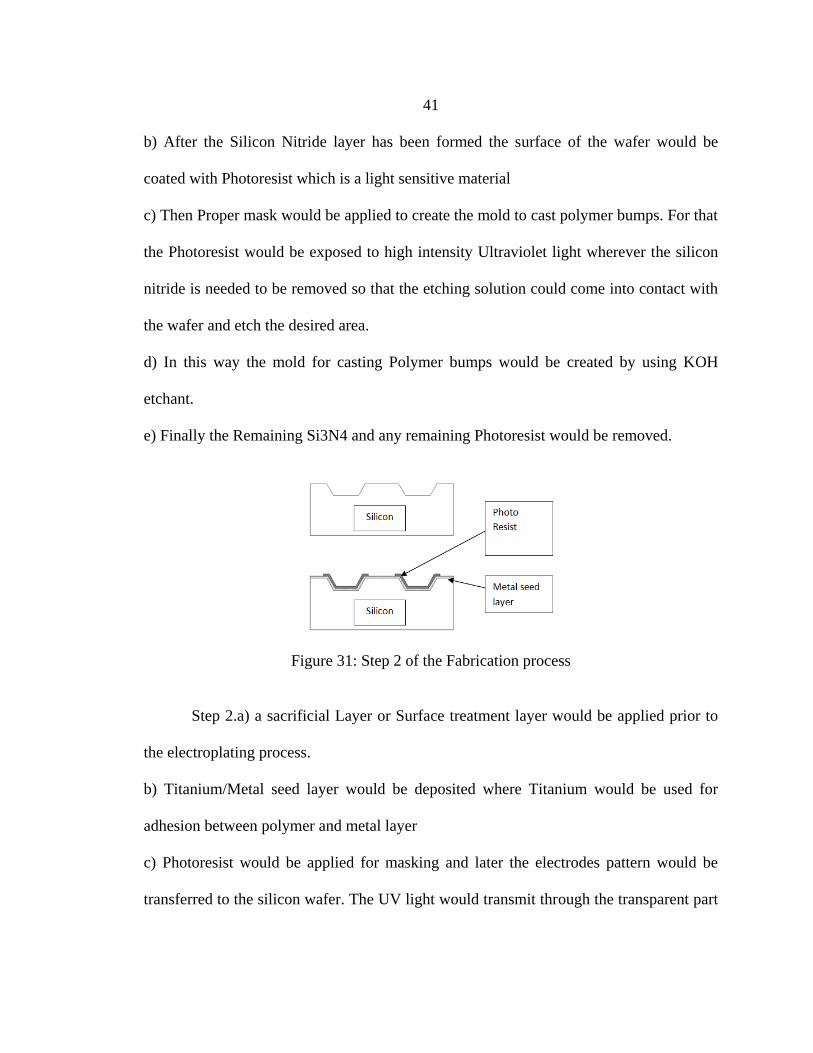
41
b) After the Silicon Nitride layer has been formed the surface of the wafer would be
coated with Photoresist which is a light sensitive material
c) Then Proper mask would be applied to create the mold to cast polymer bumps. For that
the Photoresist would be exposed to high intensity Ultraviolet light wherever the silicon
nitride is needed to be removed so that the etching solution could come into contact with
the wafer and etch the desired area.
d) In this way the mold for casting Polymer bumps would be created by using KOH
etchant.
e) Finally the Remaining Si3N4 and any remaining Photoresist would be removed.
Figure 31: Step 2 of the Fabrication process
Step 2.a) a sacrificial Layer or Surface treatment layer would be applied prior to
the electroplating process.
b) Titanium/Metal seed layer would be deposited where Titanium would be used for
adhesion between polymer and metal layer
c) Photoresist would be applied for masking and later the electrodes pattern would be
transferred to the silicon wafer. The UV light would transmit through the transparent part

42
of the mask and react with the Photoresist which would be later developed with the help
of developer solution and eventually expose the metal seed layer.
Step 3a) Metallization by electroplating technique would Produce Upper and
lower electrodes layer
b) Then Polymer material would be casted by spin coating technique on top of the metal
layers in silicon wafer as shown in Figure 32.
Figure 32: Step 3 of the Fabrication process
Figure 33: Step 4 of the Fabrication process
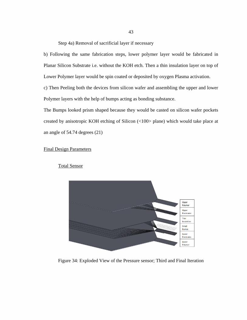
43
Step 4a) Removal of sacrificial layer if necessary
b) Following the same fabrication steps, lower polymer layer would be fabricated in
Planar Silicon Substrate i.e. without the KOH etch. Then a thin insulation layer on top of
Lower Polymer layer would be spin coated or deposited by oxygen Plasma activation.
c) Then Peeling both the devices from silicon wafer and assembling the upper and lower
Polymer layers with the help of bumps acting as bonding substance.
The Bumps looked prism shaped because they would be casted on silicon wafer pockets
created by anisotropic KOH etching of Silicon (<100> plane) which would take place at
an angle of 54.74 degrees (21)
Final Design Parameters
Total Sensor
Figure 34: Exploded View of the Pressure sensor; Third and Final Iteration

44
The Pressure sensor was modified for the third times based on the above
fabrication steps and later it was tweaked based on some recommendations. The
dimensions of the sensor were again modified to optimum values although the original
dimension of the main sensor area was unaltered from the second design iteration which
was 1.2 by 4 mm. The description of each layer is given below:
Upper and Lower Polymer Layer
Figure 35: Upper and Lower Polymer Layer Final Version; All units in mm
The dimension of the original capacitive sensing area was kept as before but the
area where it would encapsulate all the circuit wirings and connection terminals were
adjusted to an optimum dimension of 15X15 mm with the top edges at an inclined
position to coincide with the lower end of the rectangular sensor shown in Figure 35. The
ascending nature of the edges would allow the sensor to be inserted in the mouse knee
joint more conveniently without interference. The reduced dimension compared to the
2nd iteration of design would allow at least two of these sensors to be fabricated on a

45
100mm silicon wafer which would yield two sensors instead of one with the same
amount of resources like masks, chemicals for etching, metal deposition for
electroplating, polymer material during spin coating deposition and reduced waste of
materials during fabrication process.
Upper and Lower Electrodes
Figure 36: Four Upper Electrodes with dimensions in mm unit; b) Sixteen lower
electrodes with Dimensions in mm unit c) Side wiring distribution of lower electrodes d)
both upper and Lower Electrodes in parallel position

46
In the third iteration of design the most notable changes were the redistribution of
the side wirings for both upper and lower electrodes. This time connecting terminals for
the upper electrodes were much more concise and compactly located and projected at the
middle of the polymer housing symmetrically as shown in Figure 36(a). On the other
hand the side wirings for the lower electrodes were projecting from both sides of the
sensor at equal number this time shown in Figure 36(b). As a result it was possible to
avoid overlapping of connecting terminals of upper and lower electrodes completely as
shown in Figure 36(d) and the distance between the parallel wires were large enough to
avoid any substantial build up of parasitic capacitance. The dimensions of the parallel
plate capacitors were unchanged (200 X 200 microns) but the size of the connecting
terminals were changed. Both upper and lower electrodes had the same width and length
of their straight connecting terminals which were 14mm and 0.3mm respectively in
Figure 36(c) and the inclined lines were at 5.0250mm height vertically from the base of
the sensor projecting out symmetrically (Figure 36: a and c). The air gaps between the
electrodes were similar to their width which was 0.3 mm and the distance between the
symmetric electrodes located at the middle and the center line were 0.8mm and 2mm for
upper and lower electrodes respectively.
Bump Layer Initial and Final Design
Figure 37 Continued: Bump layers for bonding process; All units in mm
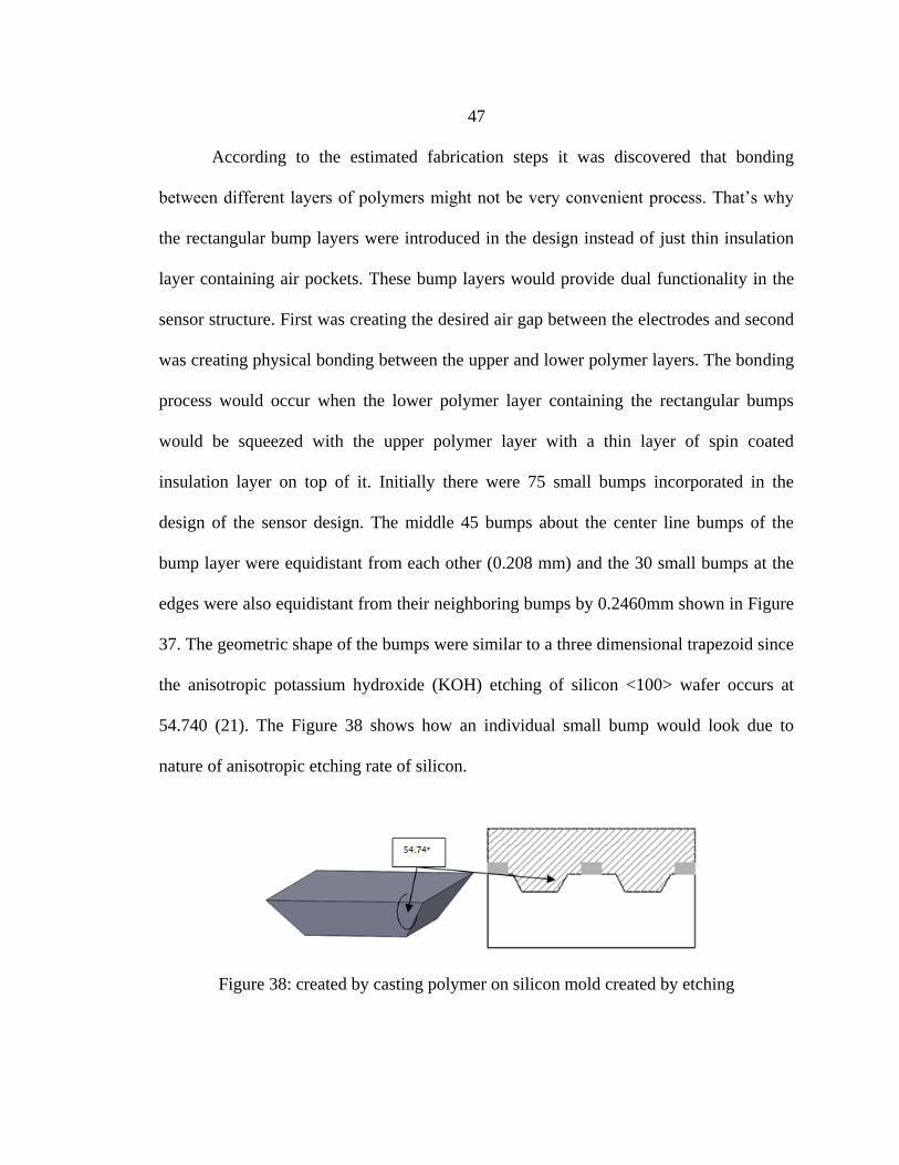
47
According to the estimated fabrication steps it was discovered that bonding
between different layers of polymers might not be very convenient process. That’s why
the rectangular bump layers were introduced in the design instead of just thin insulation
layer containing air pockets. These bump layers would provide dual functionality in the
sensor structure. First was creating the desired air gap between the electrodes and second
was creating physical bonding between the upper and lower polymer layers. The bonding
process would occur when the lower polymer layer containing the rectangular bumps
would be squeezed with the upper polymer layer with a thin layer of spin coated
insulation layer on top of it. Initially there were 75 small bumps incorporated in the
design of the sensor design. The middle 45 bumps about the center line bumps of the
bump layer were equidistant from each other (0.208 mm) and the 30 small bumps at the
edges were also equidistant from their neighboring bumps by 0.2460mm shown in Figure
37. The geometric shape of the bumps were similar to a three dimensional trapezoid since
the anisotropic potassium hydroxide (KOH) etching of silicon <100> wafer occurs at
54.740 (21). The Figure 38 shows how an individual small bump would look due to
nature of anisotropic etching rate of silicon.
Figure 38: created by casting polymer on silicon mold created by etching

48
Figure 39: Bumps layer created around the edge of the sensor
Here would be a technical difficulty due to these bump configuration which was
the pressure chambers were open on either side of the sensor as shown in the figure.
During pressure measurement inside mouse knee joint, the dissected knee needed to be
sprayed over time to time to keep it from getting dried out. Because of the spraying the
knee joint area would get wet and the sensor might also get wet when it would come into
contact with wet knee joint area. If liquid particle would get inside the capacitive cells it
would greatly alter the functionality and charge storage ability of those cells. So the
sensor surroundings needed to be insulated from any transfer of liquid. As a result a solid
continuous bump layer was designed all around the sensor structure to prevent any liquid
particle entering inside the pressure chambers except the very end where the circuit
connection terminals situated were kept open shown in Figure 40. The open end would be
located far away from the spray zone at the fixture part of the sensor. Trapped air inside
the pressure cells would travel to atmosphere through this open channel at the end of the
sensor and this would keep the pressure cells in atmospheric pressure under no load
condition. The modified bump design is shown in Figure 40.
As a result of the solid continuous bump, total numbers of small bumps were
reduced from 75 to 45 located within the matrix of capacitive cells. The solid bump

49
would seal the boundary around the edge of the sensor which was necessary for proper
functioning of the capacitive cells and it served as a good bonding media between the
wide parts of the polymer layers.
Figure 40: Solid Continuous bump around the edge along with small bumps
The 45 small bumps would provide the necessary air gap for proper operation of
each capacitive cell and the solid insulation layer will provide the dielectric medium as
well as prevent a pair of electrodes from coming into physical contact with each other
which would have greatly reduce the charge holding capacity of the electrodes.

50
Figure 41: Exploded view of the final configuration of different layers of the Sensor
Figure 42: Modified bump Layer with Continuous Solid bumps
Mask Design
The dimensional accuracy of the fabricated parts and in order to be able to
maintain that accurately through photolithography and etching processes is very
important (20). The micro patterns that we have designed would be created by
photolithography through using Photo-masks and masks are used for etching in both
surface/bulk micromachining and thin film deposition. These photmasks are physical
devices that would also need to be fabricated in order to perform photolithography. Mask

51
fabrication requires a series of photographic process and it begins with a large scale
drawing of each mask. The original mask could be 100 to 1000 times larger than the
actual feature size on the silicon wafer. The image of the desired mask would be first
created in the computer graphics system. Later an optical pattern generator would expose
the mask image directly onto a photographic plate known as reticle and an electron beam
projection system would draw the pattern directly over electron sensitive material. Reticle
images could be 1 to 10 times to its final size and a camera lens would reduce the reticle
image size to its final feature size and expose the two dimensional array of images on a
master copy of the final mask (20). The outline of mask fabrication process and the
optical exposure system is given in Figure 43 and 44 below:
Figure 43: Fabrication process outline (20)
Figure 44: Optical Exposure system of Mask to wafer: Image redrawn from textbook (20)

52
The preparation of mask is an essential step for the micro-fabrication procedure.
In order to transfer the desired pattern into the silicon wafer it would need the process-
steps and designs to be fixed at first. After the finalization of the design the pattern could
be optically transferred and projected onto the surface of the wafer as shown in figure: .
The minimum feature size that can be produced by photolithography would depend on
the wavelength of light used in the exposure (20). The exposure system could be of two
types which are contact printing and proximity/projection printing (20). Contact printing
might yield high resolution pattern transfer economically in terms of research and
prototyping but the projection printing on wafer is still most widely utilized and practiced
(20). Contact printing could damage the surface of the mask and wafer both. On the other
hand the mask would be brought into very close proximity of the wafer in projection
printing method but no contact would be made with wafer during exposure thereby
preventing damage to the mask (20). When designing the mask in the computer graphics
system it would need some rules to be followed like alignment marks, trace size,
dimensional consistency, repeatability, reusability and cost effectiveness.
From the fabrication steps of the third and final design it was evident that it would
require two masks for the metallization process and one mask for the bumps layer by
etching cavity on the silicon wafer. For the structural encapsulation with polymer
material it would not require a mask since we would not be etching any polymer material
instead it would be deposited by spin coating method over the etched cavity on silicon
wafer which would create bumps layer. Later with the help of alignment marks the
outside geometry would be cut according to the pattern dimension. The thickness of the

53
spin coated polymer material would be controlled by controlling the RPM (Revolution
per minute) of the platform of spin coating machine and time of spin coating process
according to the manufacturer specifications of the material.
The designed masks created in the CAD system would be presented based on the
fabrication steps for the micro-pressure sensor. The following rules were followed when
the masks were designed in the computer graphics system:
The scale of the whole drawing layout was kept in “Microns”.
All the features were drawn with respect to a 100 mm wafer system.
Whole wafer was centered with respect to the origin (zero co-ordinates) of the
layout.
All the patterns in the drawing were continuous line and closed polygon system.
The wafers were containing alignment marks so that the different masks could be
placed on the same spot and alignment marks were close to the center of the
wafer.
Both the metallization masks and bump layer mask were aligned (i.e. the devices
were on the same spot on each mask)
Metallization Masks
The metallization masks contained the pattern of upper and lower electrodes
layer. They were situated side by side on the silicon wafer so that both the upper polymer
layer containing the upper electrodes and the lower polymer layer containing the lower
electrodes would be fabricated at the same time by photo-lithography technique.
Moreover both patterns were located on the same mask so that only one mask

54
would be needed for the whole metallization process. In this way it would save
fabrication cost for additional masks for each individual pattern and this approach would
yield cost effectiveness. From the Figure 45, it is evident that the clear part (transparent
part) of the masks is the pattern we would like to print on the silicon wafer and anything
outside the transparent part would remain under photoresist since the photoresist that
would not come into contact with UV (Ultra violet) ray would remain intact and un-
developed. Therefore the geometry below the photoresist would not have any
metallization process except the clear part where the photoresist would come into contact
with UV ray and later developed and removed exposing the seed layer. As a result the
transparent exposed part of the wafer through the mask would undergo deposition of
metals through electroplating process with the help of exposed seed layer. The Figure 45
and 46(a) shows the upper and lower electrodes Mask on the same wafer with the solid
hatch line being applied to indicate which part of the mask would be opaque and which
part would remain clear.
Figure 45: Illustration of opaque and transparent part of the metallization masks Left one
for Upper and Right one for lower Electrodes
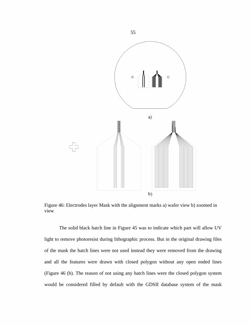
55
Figure 46: Electrodes layer Mask with the alignment marks a) wafer view b) zoomed in
view
The solid black hatch line in Figure 45 was to indicate which part will allow UV
light to remove photoresist during lithographic process. But in the original drawing files
of the mask the hatch lines were not used instead they were removed from the drawing
and all the features were drawn with closed polygon without any open ended lines
(Figure 46 (b). The reason of not using any hatch lines were the closed polygon system
would be considered filled by default with the GDSII database system of the mask

56
making machines. That’s why the masks were designed as a bright field since it would be
inverted at the mask making machine which would create dark filled zones in the mask.
Bump Extrusion Mask
The bump layer mask contained only a single feature in contrast to two features in
the metallization mask. In this case the bump layout was closer to the right alignment
mark which would make the feature exactly aligned with the traces of lower electrodes
as shown in figure: . The bumps would be created by anisotropic etching of silicon wafer
with KOH solution so UV light needed to be passed through wherever we wanted the
holes to be created on the silicon wafer defined by the mask. The clear zone will allow
UV light according to the pattern of the continuous solid bumps and forty five small
bumps to react with the photoresist applied on silicon wafer shown in Figure 47. After
reaction with the PR it will be developed and removed by developer solution thereby
exposing those locations on the silicon wafer to be etched and bump shaped holes to be
created. The dark zones would not allow any UV light thereby the PR on that region
would be undeveloped and silicon surface under the PR would stay intact and not be
exposed.
Figure 47: Illustration of opaque and transparent zone of the bump layer Mask

57
Figure 48: Layer Mask with the alignment marks a) wafer view b) zoomed in view
Figure 49: Mask Alignment in progress: a) The bump layer mask is brought near metal
layer mask b) the alignment marks are about to be overlapped on each other

58
The features in the bump layer mask were kept close to the right alignment mark
shown in Figure 48(a) and (b) in such a way that it was exactly in the same position as
the lower electrodes feature were located on the metallization mask. As a result the
bumps could be easily created below the lower electrodes according to the designed
fabrication process steps. The bump mask could have been easily accommodated on the
metallization mask but it was designed separately as an individual mask because the
creation of the bump layer involved separate process steps compared to the electroplating
and metal deposition process. According to the profile of the features on these masks it
could be easily estimated that the process steps would yield at least two fully functional
identical sensors (shown in Figure 46(a)) after the end of each individual fabrication
process.

59
MATERIAL SELECTION
There are different types of materials that can be used in building Microsystems.
But selecting the appropriate material based on proper application is paramount. One
major criteria for selecting the right material is to follow the process flow designed for
the particular requirements such as etchants, thin film deposition etc (5). Since our
photolithography process for the fabrication of micro-pressure-sensor involved polymer
as the passive substrate material and metals as the active substrate material as well as
sensing component in the Microsystems we will be concentrating mainly on those two
categories. We will also consider a composite polymer structure in our material selection
process of the pressure sensor.
Polymers
Polymers have become increasingly popular material for Microsystems and
MEMS in diverse application such as micro fluidic systems, biomedical devices, pressure
sensors, tactile sensors and so on. Polymers have been conventionally used as insulators,
sheathing, and capacitor encapsulation in electronic devices and die pads in IC’s (5). Few
advantages of polymers as structural material are light weight, electrical non
conductivity, high corrosion resistance, high flexibility in structures and ease of
processing. Thin polymer films are also used as electric insulators in micro-devices and
as a dielectric substance in micro-capacitors. They are ideal material for shielding against
electromagnetic and radio frequency interference and widely used for packaging of other
Microsystems (5).

60
The primary features that we were looking for during our material selection
process were: flexibility, ease of fabrication process, ease of availability, economical
feasibility, ease of machining, chemically inertness or non-reactive, good insulation and
dielectric properties, good adhesiveness and ease of bonding or good bonding
characteristics and above all biocompatibility. For our micro pressure sensor we primarily
considered two types of polymer materials from the perspective of above mentioned
characteristics. We considered Polyimide and PDMS (Polydimethylsiloxane) as two
possible candidates for the structural material as well as insulation and dielectric medium
of the sensor.
PDMS
It is an acronym for Polydimethylsiloxane which is a silicone elastomer: is
primarily used for embedding electronic components through casting in order to prolong
lifespan (22). It acts as a dielectric insulator and protects the components from influences
of environment, mechanical shock and vibration within a large temperature range (-50 to
2000C). It has been used in Micro and nanotechnologies since 1995 due to its good
contour accuracy (<10nm) (22). It has become one of the most popular materials in micro
Total analysis system (µ TAS) and polymer MEMS due to its attractive features such as
flexibility, elasticity, transparency and biocompatibility (23). Flexible and elastic features
are utilized effectively in pneumatic balloon actuator (PBA), piston mirror array device
(PMA), micro pump for µ TAS devices, fluidics (valves, pumps, fluidic circuits) (23)
and optical systems such as adaptive lenses, tilting mirrors, (22) and other sensors such as
acceleration sensors, tactile sensors, chemical sensors and medical sensors (22).

61
The dielectric constant and elasticity of the dielectric layer as well of the
embedding structure determines the sensitivity of the pressure sensor and they influence
the mechanical and electrical properties of a micro-sensor (25). The attractive flexibility,
good dielectric property and linear elastic behavior might be suitable for the construction
of the capacitive type micro-electronic pressure sensor. Some analysis based on elastic
properties of PDMS, relative capacitive changes in the PDMS based structure, stress
analysis simulation of the designed sensor with PDMS as the structural material would be
presented in the later chapters. The mechanical properties of PDMS found in various
journal articles would be discussed and capacitive characteristics under applied pressure
would be analyzed.
The structural properties of polymer networks are highly dependent to the
reaction by which they are formed (24). It is essential to know about the imperfections in
the network structure of polymers caused by cross linking in order to interpret their
modulus of elasticity properly (24). The elasticity of PDMS is tunable by different
mixing ratios of the PDMS pre-polymer and the curing agent during formation (25). The
ideal property of PDMS for our micro pressure sensor would be to have linear modulus
of elasticity and Poisson’s ratio. The PDMS stress-strain characteristics have been
investigated in (25) in-order to select a suitable mixing ratio for the insulation layer of the
sensor (25). The characterization procedure of the PDMS involved making cylindrical
PDMS samples by degassing the pre-polymer and curing agent in a vacuum chamber and
pouring into pre-fabricated cylindrical mold described in (25).Then each specimens made
by different mixing ratios were baked at 70 C for around two hours (25). The cylindrical

62
PDMS samples were subjected to uni-axial tensile test to find out stress-strain
relationship of five mixing ratio samples in (25). The five mixing ratios of the PDMS pre-
polymer and the curing agent performed in (25) resulted in different stiffness values of
PDMS and the stiffness increased as the portion of the PDMS pre-polymer increased in
the mixture (25). The stress-strain relationship acquired in (25) were non linear for the
mixtures containing high PDMS pre-polymer (25). The stress strain data of five different
mixtures of PDMS pre-polymer and curing agent will give the selection of the proper
mixing ratio based on the operating pressure range of our micro-pressure sensor. The
graphical representation of the summary of the stress-strain relationship published in (25)
is given in Figure 50 below:
Figure 50: The stress vs. strain curves of PDMS specimens with five different mixing
ratios of the pre-polymer and curing agent (12:1, 16:1, 20:1, 24:1, and 28:1); image
modified from (25)
Based on the operating pressure range of the sensor, It can decided on selecting
the proper mixing ratio of the PDMS that would yield highest linearity and highest

63
elasticity from the above graph. From Table 4 and free body diagram as well, it was
clearly evident that our maximum external applied pressure on the mouse knee would
result at 25% contact area for 50 gm load which was equivalent to 464 kPa (rounded
figure) or 0.464 MPa of pressure (Force over area). Since the interested range of pressure
was between 0.4 and 0.5 MPa the optimum highest linearity of stress-strain relationship
within this desired pressure zone could be found by 12:1 mixing ratio of PDMS pre-
polymer and curing agent. The capacitance vs. pressure characteristic graph would be
plotted for PDMS as the structural material. A certain gap between the parallel plate
capacitor was considered, started with zero loads and the initial capacitance between the
parallel plates sandwiching PDMS as dielectric material was calculated as well as PDMS
as embedding material in the top and bottom layer. Then the gaps were descended step by
step until it was completely closed. The capacitances as well as change of capacitance
with respect to initial capacitance at each step of gap changes and final capacitance value
at closed condition were calculated.
The article in (22) has discussed and characterized the mechanical properties of
PDMS elastomer. The mixing ratio of PDMS in (22) was 10:1 for two most commonly
used silicones: RTV 615 and Sylgard 184 with hardener solution. According to the
experimental work in (22) they have found a larger linear behavior of room-temperature-
vulcanized (RTV) silicones up to a strain of 100%. The experimental stress-strain
diagram obtained from (22) is given in Figure 51. From the graph it is clearly discernible
that both silicone polymers exhibit a linear stress-strain relationship up to a strain of 45%
which corresponded to a constant elastic modulus of 1.76 MPa for Sylgard 184 and 1.54
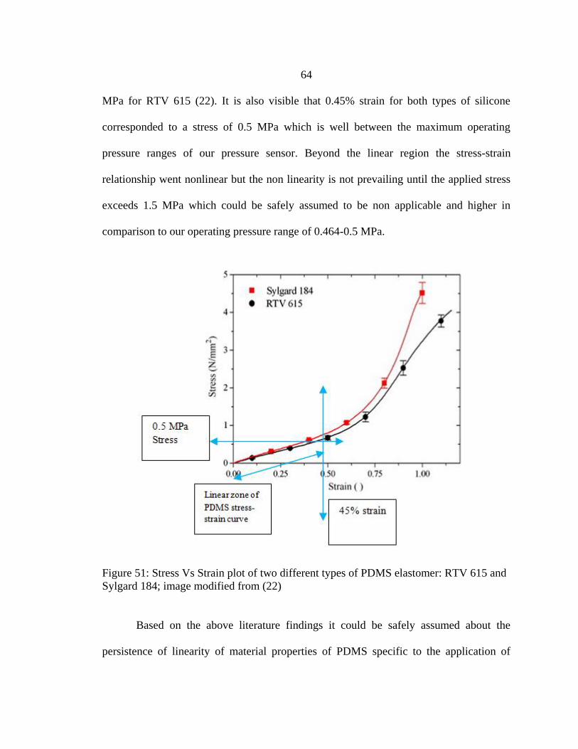
64
MPa for RTV 615 (22). It is also visible that 0.45% strain for both types of silicone
corresponded to a stress of 0.5 MPa which is well between the maximum operating
pressure ranges of our pressure sensor. Beyond the linear region the stress-strain
relationship went nonlinear but the non linearity is not prevailing until the applied stress
exceeds 1.5 MPa which could be safely assumed to be non applicable and higher in
comparison to our operating pressure range of 0.464-0.5 MPa.
Figure 51: Stress Vs Strain plot of two different types of PDMS elastomer: RTV 615 and
Sylgard 184; image modified from (22)
Based on the above literature findings it could be safely assumed about the
persistence of linearity of material properties of PDMS specific to the application of

65
pressure sensor during stress and structural analysis using finite element method and
during comparisons with other polymer materials for material selection.
It was required during the fabrication process to spin coat the structural polymer
over silicon substrate to achieve a desired thickness of the upper and lower polymer
layers of the pressure sensor. The thickness largely depended on viscosity and the spin
curve which is a rotational frequency dependent layer thickness (22). In a typical spin
curve for PDMS the relation between the thickness and rotational frequency is hyperbolic
which typically indicates that a thicker layer will result with small RPM (Revolution per
minute) and a thinner layer will result through higher rotational frequency (22). The spin
curve of RV 615 and Sylgard 184 is illustrated in the Figure 52 below.
Figure 52: The exponential curve fit of Thickness Vs frequency of two PDMS silicone
polymer; image modified from (22)
The dielectric constant of PDMS ranges from 2.3-2.8 (26). So compared with
same dimension of two parallel plates with same gap distance PDMS would generate
more capacitance compare to air (25) if it was filled as dielectric material in between the

66
parallel plates since the dielectric constant of air is 1 (25). The Poisson’s ratio and tensile
(fracture) strength for standard PDMS was found in (26) as 0.5 and 2.24 MPa
respectively.
Polyimide
Polyimide is another widely used material in micro-electronics fabrication
originally developed by the DuPont chemical company in 1950’s as high temperature
polymers (commercially known as kapton polyimide)(30) used as multilevel interconnect
technologies and flexible circuit board substrates due to its various attractive properties
(27) like biocompatibility, electrical insulation, thermal stability and magnetic
permeability (27). It offers a low residual structural stress and offers a dynamic
Microsystems fabrication due to its durability (27). Polyimide films (Abbreviated PI) are
also used on wafers as passivation layers, stress buffer layers, dry etch masks, structural
layers and re-distribution layers for chip scale and wafer level packaging (28). Polyimide
films are cured at very high temperature (350-400oC) to ensure proper mechanical and
electrical properties (28). Polyimide film deposition can be done by conventional micro-
fabrication techniques like spin coating method and curing at 300oC in nitrogen
atmosphere for certain amount of time (27). The tensile stress-strain relationship of
polyimide film is given in Figure 53:

67
Figure 53: Stress Vs Strain plot of polyimide( containing m-catenatedphenylene rings)
tensile test (29); image modified from (29)
The elastic modulus from the above stress-strain diagram for polyimide film
received was 1.46 GPa with tensile strength of 10.02 MPa (29). The mechanical
properties found for polyimide from the original manufacturer of this product is given
below:
Figure 54: Stress-strain Diagram of Dupont kapton polyimide from the data sheet of
original manufacturer (31); image modified from (31)

68
From the above stress-strain diagram for Dupont Kapton polyimide it can
observed that the linear portion of the diagram is situated within the range of
approximately 2% mechanical strain and the rest of the region is quite non linear. But the
stress-strain plot will stay linear within 0-6 MPa as evident from Figure 54 which is
conveniently within the operating range of the pressure sensor which is 0.463-0.5 MPa.
The modulus of elasticity from the manufacturer data could be found as 2.5 GPa (at 23
oC) (31) and yield strength of 231 MPa (at 23
oC) with Poisson’s ratio of 0.34 (at 23
oC)
(31). The dielectric constant for kapton polyimide of thickness ranging from 75-125 µm
was found to be 3.5 (31). Polyimide film thickness could be easily controlled during
micro-fabrication process by controlling speed of the spin chuck and time according to
manufacturer (Dupont) specifications found in (32).
Sample calculation of Sensitivity of the sensor with PDMS as structural and insulation
Material:
From equation 4 of Parallel plate capacitors: capacitance C is given by
Where C is capacitance in the parallel plate capacitor, ϵo is permittivity of free space
(vacuum); ϵo = 8.854 picoFarad/meter; and ϵr is the relative permittivity of the dielectric
medium (5).
In our pressure sensor, Overlapped area between the parallel plates, A=
(200X200) µm2 = 40000 µm
2, Initial Gap do = 12 µm, relative permittivity for PDMS as
dielectric medium, ϵr = 2.8, for initial gap of do, Initial Capacitance,
Co= ϵo ϵr A/do = (8.854*10-12
Farad)* 2.8* (40000*10-12
meter2)/ (12*10
-6 meter)

69
= (8.263*10-14
) Farad
= 82.63 femtoFarad
For PDMS polymer, Average Elastic Modulus, E = 1760 kPa with an initial knee
pressure of 34.474 kPa; Linear Strain, ε = (σ/E) = (34.474/1760) = 0.0195875
Figure 55: Change of Capacitance in a Parallel Plate capacitor
As a result, Change of Gap between the parallel plates after applied pressure of 34.474
kPa, d1= do-Δd=12-(12*ε) =11.764
So, final capacitance after the applied pressure of 34.4745 kPa, C1= (8.854*10-12
Farad/meter)* 2.8* (40000*10-12
meter2)/ (11.764*10
-6 meter)
=84.295 femtoFarad
So, Change of capacitance, ΔC = C1- Co = 1.665 femtoFarad.
The sensitivity of the sensor was calculated using Equation 5 found in (5) :
Equation 5
Where Vin is a constant supplied voltage and Vo is output voltage corresponding
to the change of capacitances, C is a known capacitance value and ΔC is the change of
capacitance in the micro-pressure sensor. In this way the theoretical change of
capacitances with respect to our applied range of pressure from 34.474 kPa to 463.543

70
kPa was calculated to observe sensitivity of the sensor (Vo/Vin) and for both PDMS and
Polyimide as structural material and tabulated the data in Table 5 and 6 and graphs in
Figure 57 to 61.
Table 5: Calculation of Change of Capacitance and Sensitivity of the Sensor for PDMS
Die
lect
ric
Mat
eria
l
Nam
e
You
ng'
s
Mo
du
lus(
Kp
a),
PD
MS
Rel
ativ
e
Per
mit
tivi
ty(ϵ
r )
Init
ial G
ap d
o(µ
m)
Pro
ject
ed P
late
area
(µm
2)
Ap
plie
d K
nee
Pre
ssu
re (
KP
a)
Per
mit
tivi
ty in
vacu
um
,ϵ0
(Far
ad/m
ete
r)
Init
ial
Cap
acit
ance
(Co)
(Fem
toFa
rad
)
Stra
ins
in P
DM
S, ε
Gap
aft
er a
pp
lied
stre
ss,d
1(µ
m)
Fin
al
Cap
acit
ance
(C1
)(Fe
mto
Fara
d)
Ch
ange
of
cap
acit
ance
(C1-
Co)(
Fem
toFa
rad
)
Vo
ltag
e R
atio
V0/V
i n
1.76E
+03
2.
8 12
4000
0
34.4
74
8.85E
-12 82.6373
0.019
6
11.76
50
84.28
83
1.651
0
0.005
0
1.76E
+03
2.
8 12
4000
0
45.7
65
8.85E
-12 82.6373
0.026
0
11.68
80
84.84
35
2.206
2
0.006
6
1.76E
+03
2.
8 12
4000
0
48.7
76
8.85E
-12 82.6373
0.027
7
11.66
74
84.99
28
2.355
5
0.007
0
1.76E
+03
2.
8 12
4000
0
55.9
27
8.85E
-12 82.6373
0.031
8
11.61
87
85.34
95
2.712
1
0.008
1
1.76E
+03
2.
8 12
4000
0
57.0
56
8.85E
-12 82.6373
0.032
4
11.61
10
85.40
61
2.768
7
0.008
2
1.76E
+03
2.
8 12
4000
0
63.0
78
8.85E
-12 82.6373
0.035
8
11.56
99
85.70
92
3.071
8
0.009
1
1.76E
+03
2.
8 12
4000
0
68.3
48
8.85E
-12 82.6373
0.038
8
11.53
40
85.97
61
3.338
8
0.009
9
1.76E
+03
2.
8 12
4000
0
77.3
81
8.85E
-12 82.6373
0.044
0
11.47
24
86.43
77
3.800
3
0.011
2
1.76E
+03
2.
8 12
4000
0
79.6
39
8.85E
-12 82.6373
0.045
2
11.45
70
86.55
38
3.916
5
0.011
6
1.76E
+03
2.
8 12
4000
0
90.9
30
8.85E
-12 82.6373
0.051
7
11.38
00
87.13
94
4.502
0
0.013
3
1.76E
+03
2.
8 12
4000
0
98.8
34
8.85E
-12 82.6373
0.056
2
11.32
61
87.55
40
4.916
7
0.014
4
1.76E
+03
2.
8 12
4000
0
102.
221
8.85E
-12 82.6373
0.058
1
11.30
30
87.73
29
5.095
6
0.015
0
1.76E
+03
2.
8 12
4000
0
105.
985
8.85E
-12 82.6373
0.060
2
11.27
74
87.93
25
5.295
2
0.015
5
1.76E
+03
2.
8 12
4000
0
113.
513
8.85E
-12 82.6373
0.064
5
11.22
61
88.33
45
5.697
2
0.016
7
1.76E
+03
2.
8 12
4000
0
120.
287
8.85E
-12 82.6373
0.068
3
11.17
99
88.69
95
6.062
2
0.017
7
1.76E
+03
2.
8 12
4000
0
124.
804
8.85E
-12 82.6373
0.070
9
11.14
91
88.94
45
6.307
2
0.018
4
1.76E
+03
2.
8 12
4000
0
134.
590
8.85E
-12 82.6373
0.076
5
11.08
23
89.48
00
6.842
7
0.019
9
1.76E
+03
2.
8 12
4000
0
136.
095
8.85E
-12 82.6373
0.077
3
11.07
21
89.56
30
6.925
6
0.020
1

71
PDMS
Table 5 Continued 1.76E
+03
2.
8 12
4000
0
141.
741
8.85E
-12 82.6373
0.080
5
11.03
36
89.87
54
7.238
1
0.021
0
1.76E
+03
2.
8 12
4000
0
147.
386
8.85E
-12 82.6373
0.083
7
10.99
51
90.19
01
7.552
7
0.021
9
1.76E
+03
2.
8 12
4000
0
148.
892
8.85E
-12 82.6373
0.084
6
10.98
48
90.27
43
7.637
0
0.022
1
1.76E
+03
2.
8 12
4000
0
163.
194
8.85E
-12 82.6373
0.092
7
10.88
73
91.08
29
8.445
6
0.024
3
1.76E
+03
2.
8 12
4000
0
177.
496
8.85E
-12 82.6373
0.101
0
10.78
98
91.90
61
9.268
8
0.026
6
1.76E
+03
2.
8 12
4000
0
184.
648
8.85E
-12 82.6373
0.105
0
10.74
10
92.32
33
9.686
0
0.027
7
1.76E
+03
2.
8 12
4000
0
206.
101
8.85E
-12 82.6373
0.117
0
10.59
48
93.59
79
10.96
06
0.031
1
1.76E
+03
2.
8 12
4000
0
227.
554
8.85E
-12 82.6373
0.129
0
10.44
85
94.90
82
12.27
09
0.034
6
1.76E
+03
2.
8 12
4000
0
249.
008
8.85E
-12 82.6373
0.141
0
10.30
22
96.25
58
13.61
84
0.038
1
1.76E
+03
2.
8 12
4000
0
291.
915
8.85E
-12 82.6373
0.166
0
10.00
97
99.06
90
16.43
16
0.045
2
1.76E
+03
2.
8 12
4000
0
334.
821
8.85E
-12 82.6373
0.190
0
9.717
1
102.0
516
19.41
42
0.052
6
1.76E
+03
2.
8 12
4000
0
377.
728
8.85E
-12 82.6373
0.215
0
9.424
6
105.2
193
22.58
20
0.060
1
1.76E
+03
2.
8 12
4000
0
420.
635
8.85E
-12 82.6373
0.239
0
9.132
0
108.5
901
25.95
27
0.067
9
1.76E
+03
2.
8 12
4000
0
463.
542
8.85E
-12 82.6373
0.263
0
8.839
5
112.1
839
29.54
65
0.075
8
Table 6: Calculation of Change of Capacitance and Sensitivity of the Sensor For
Polyimide
Die
lect
ric
Mat
eria
l Nam
e
You
ng'
s M
od
ulu
s(K
pa)
,
PD
MS
Rel
ativ
e P
erm
itti
vity
(ϵr
) In
itia
l Gap
do
(µm
)
Pro
ject
ed P
late
are
a(µ
m2
)
Ap
plie
d K
nee
Pre
ssu
re
(Kp
a)
Per
mit
tivi
ty in
vac
uu
m,ϵ
0
(Far
ad/m
ete
r)
Init
ial C
apac
itan
ce(C
o)
(Fem
toFa
rad
)
Stra
ins
in P
DM
S, ε
Gap
aft
er a
pp
lied
stre
ss,d
1(µ
m)
Fin
al
Cap
acit
ance
(C1
)(Fe
mto
Fara
d)
Ch
ange
of
cap
acit
ance
(C1
-
Co
)(Fe
mto
Fara
d)
Vo
ltag
e R
atio
V0
/Vin
2.50E
+06
3.
5 12
4000
0
34.4
74
8.85E
-12
103.29
667
1.38E-
05
11.999
83453
103.2
9809
0.0014
2
0.00
0003
4
2.50E
+06
3.
5 12
4000
0
45.7
65
8.85E
-12
103.29
667
1.83E-
05
11.999
78033
103.2
9856
0.0018
9
0.00
0004
6
2.50E
+0
3.
5 12
4000
0
48.7
76
8.85E
-12
103.29
667
1.95E-
05
11.999
76587
103.2
9868
0.0020
2 0.0000
049
72
P
ol
yi
m
Table 6 Continued
2.50E
+06
3.
5 12
4000
0
55.9
27
8.85E
-12
103.29
667
2.24E-
05
11.999
73155
103.2
9898
0.0023
1
0.00
0005
6
2.50E
+06
3.
5 12
4000
0
57.0
56
8.85E
-12
103.29
667
2.28E-
05
11.999
72613
103.2
9902
0.0023
6
0.00
0005
7
2.50E
+06
3.
5 12
4000
0
63.0
78
8.85E
-12
103.29
667
2.52E-
05
11.999
69722
103.2
9927
0.0026
1
0.00
0006
3
2.50E
+06
3.
5 12
4000
0
68.3
48
8.85E
-12
103.29
667
2.73E-
05
11.999
67193
103.2
9949
0.0028
2
0.00
0006
8
2.50E
+06
3.
5 12
4000
0
77.3
81
8.85E
-12
103.29
667
3.10E-
05
11.999
62857
103.2
9986
0.0032
0
0.00
0007
7
2.50E
+06
3.
5 12
4000
0
79.6
39
8.85E
-12
103.29
667
3.19E-
05
11.999
61773
103.2
9996
0.0032
9
0.00
0008
0
2.50E
+06
3.
5 12
4000
0
90.9
30
8.85E
-12
103.29
667
3.64E-
05
11.999
56354
103.3
0042
0.0037
6
0.00
0009
1
2.50E
+06
3.
5 12
4000
0
98.8
34
8.85E
-12
103.29
667
3.95E-
05
11.999
52560
103.3
0075
0.0040
8
0.00
0009
9
2.50E
+06
3.
5 12
4000
0
102.
221
8.85E
-12
103.29
667
4.09E-
05
11.999
50934
103.3
0089
0.0042
2
0.00
0010
2
2.50E
+06
3.
5 12
4000
0
105.
985
8.85E
-12
103.29
667
4.24E-
05
11.999
49127
103.3
0105
0.0043
8
0.00
0010
6
2.50E
+06
3.
5 12
4000
0
113.
513
8.85E
-12
103.29
667
4.54E-
05
11.999
45514
103.3
0136
0.0046
9
0.00
0011
4
2.50E
+06
3.
5 12
4000
0
120.
287
8.85E
-12
103.29
667
4.81E-
05
11.999
42262
103.3
0164
0.0049
7
0.00
0012
0
2.50E
+06
3.
5 12
4000
0
124.
804
8.85E
-12
103.29
667
4.99E-
05
11.999
40094
103.3
0182
0.0051
6
0.00
0012
5
2.50E
+06
3.
5 12
4000
0
134.
590
8.85E
-12
103.29
667
5.38E-
05
11.999
35397
103.3
0223
0.0055
6
0.00
0013
5
2.50E
+06
3.
5 12
4000
0
136.
095
8.85E
-12
103.29
667
5.44E-
05
11.999
34674
103.3
0229
0.0056
2
0.00
0013
6
2.50E
+06
3.
5 12
4000
0
141.
741
8.85E
-12
103.29
667
5.67E-
05
11.999
31964
103.3
0252
0.0058
6
0.00
0014
2
2.50E
+06
3.
5 12
4000
0
147.
386
8.85E
-12
103.29
667
5.90E-
05
11.999
29255
103.3
0276
0.0060
9
0.00
0014
7
73
id
e
Table 6 Continued
2.50E
+06
3.
5 12
4000
0
148.
892
8.85E
-12
103.29
667
5.96E-
05
11.999
28532
103.3
0282
0.0061
5
0.00
0014
9
2.50E
+06
3.
5 12
4000
0
163.
194
8.85E
-12
103.29
667
6.53E-
05
11.999
21667
103.3
0341
0.0067
4
0.00
0016
3
2.50E
+06
3.
5 12
4000
0
177.
496
8.85E
-12
103.29
667
7.10E-
05
11.999
14802
103.3
0400
0.0073
3
0.00
0017
8
2.50E
+06
3.
5 12
4000
0
184.
648
8.85E
-12
103.29
667
7.39E-
05
11.999
11369
103.3
0430
0.0076
3
0.00
0018
5
2.50E
+06
3.
5 12
4000
0
206.
101
8.85E
-12
103.29
667
8.24E-
05
11.999
01072
103.3
0518
0.0085
2
0.00
0020
6
2.50E
+06
3.
5 12
4000
0
227.
554
8.85E
-12
103.29
667
9.10E-
05
11.998
90774
103.3
0607
0.0094
0
0.00
0022
8
2.50E
+06
3.
5 12
4000
0
249.
008
8.85E
-12
103.29
667
9.96E-
05
11.998
80476
103.3
0696
0.0102
9
0.00
0024
9
2.50E
+06
3.
5 12
4000
0
291.
915
8.85E
-12
103.29
667
1.17E-
04
11.998
59881
103.3
0873
0.0120
6
0.00
0029
2
2.50E
+06
3.
5 12
4000
0
334.
821
8.85E
-12
103.29
667
1.34E-
04
11.998
39286
103.3
1050
0.0138
4
0.00
0033
5
2.50E
+06
3.
5 12
4000
0
377.
728
8.85E
-12
103.29
667
1.51E-
04
11.998
18690
103.3
1228
0.0156
1
0.00
0037
8
2.50E
+06
3.
5 12
4000
0
420.
635
8.85E
-12
103.29
667
1.68E-
04
11.997
98095
103.3
1405
0.0173
8
0.00
0042
1
2.50
E+06
3.
5 12
4000
0
463.
542
8.85E
-12
103.29
667
1.85E-
04
11.997
77500
103.3
1582
0.0191
6
0.00
0046
4

74
Figure 56: Plot of Sensitivity Vs Applied Pressure; Material PDMS
Figure 57: Plot of Sensitivity Vs Applied Pressure; Material Polyimide
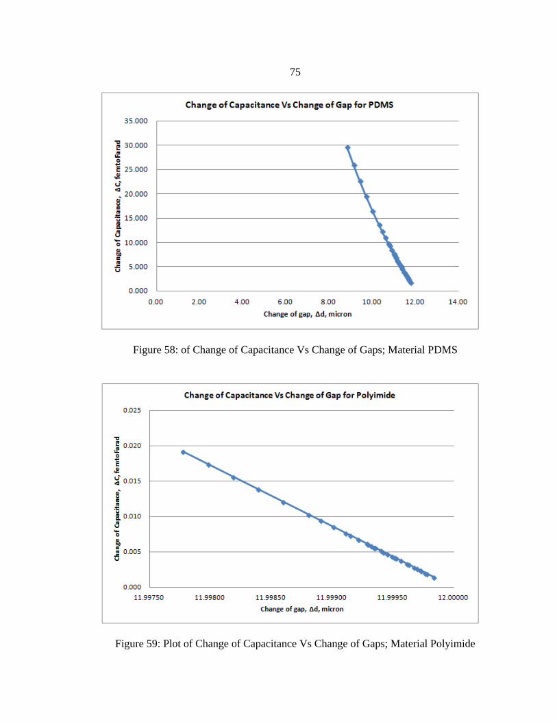
75
Figure 58: of Change of Capacitance Vs Change of Gaps; Material PDMS
Figure 59: Plot of Change of Capacitance Vs Change of Gaps; Material Polyimide
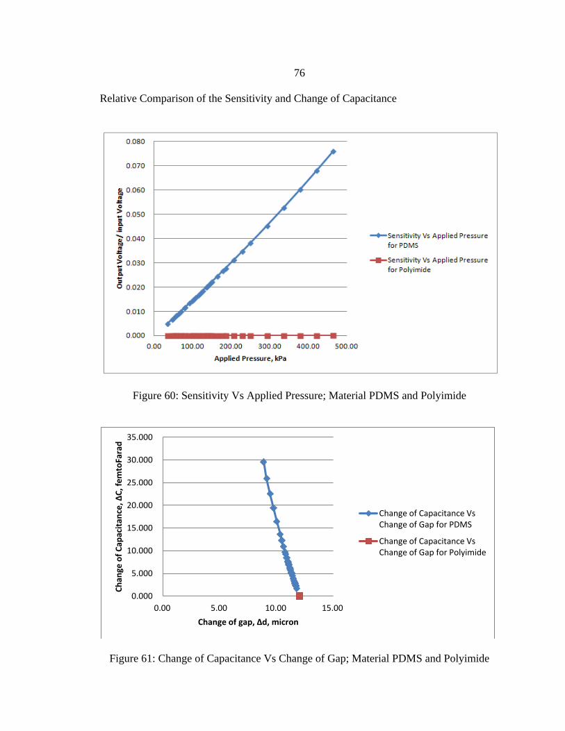
76
Relative Comparison of the Sensitivity and Change of Capacitance
Figure 60: Sensitivity Vs Applied Pressure; Material PDMS and Polyimide
Figure 61: Change of Capacitance Vs Change of Gap; Material PDMS and Polyimide
0.000
5.000
10.000
15.000
20.000
25.000
30.000
35.000
0.00 5.00 10.00 15.00
Ch
ange
of
Cap
acit
ance
, ΔC
, fe
mto
Fara
d
Change of gap, Δd, micron
Change of Capacitance Vs Change of Gap for PDMS
Change of Capacitance Vs Change of Gap for Polyimide

77
From Figure 56 and 57 plots we can clearly see the sensitivity of the sensor
increases almost linearly as the applied contact pressure rises inside the knee joint for
both PDMS and polyimide as structural material. On the other hand from Figure 58 and
59 we can observe that the change of capacitance is going down as the gap between the
parallel plate capacitors increases or in other words the change of capacitance increases
as the gap between the parallel plates decreases with the applied pressure which is
evident from Equation 4 where the capacitance is inversely proportional to the gap
between the parallel plates. From figure: 60 and 61 we can see a relative comparison of
sensitivity and change of capacitance of PDMS and polyimide. PDMS results in a more
responsive capacitive sensor system compare to Polyimide where the magnitude of
sensitivity was about 1648 times higher in PDMS than polyimide for an applied pressure
of 463.54 kPa. The similar thing happened in case of change of capacitance which was
1541 times higher in PDMS than Polyimide. This was obvious since the stiffness of the
polyimide was 1420 times higher than that of PDMS so PDMS resulted in a more flexible
behavior than Polyimide. So for better structural integrity, rigidity and robustness
polyimide would be a better structural material and on the other hand for greater
flexibility, sensitivity and ease of fabrication PDMS will be a good selection as both
dielectric and embedding substrate for the micro-pressure sensor.
Electrode Material
Gold and copper are most commonly used metallization materials in micro-electro
fabrication process. Selection of metal type as electrode materials would solely depend

78
on structural integrity, fracture/ micro crack resistance, higher yield point, electrical
conductivity, ease of fabrication and better bonding/adhesion with the polymer substrate.
For the capacitive type pressure sensors the sensitivity of the sensor would purely depend
on the distance between the parallel plates and the overlapped area between the plates but
not on their strength or conductivity. As the fabrication process established in earlier
chapters, the metallization would be performed on the silicon wafer but not on the
polymer substrates so it was not a matter of concern about bonding technique between the
polymer materials and metal layers since the adhesion would be purely due to
mechanically applied force and surface tension of the visco-elastic material when PDMS
or Polyimide would be spin casted over the gold/copper metal layers. A metal layer
thickness of 5-20 microns would be considered for the micro-pressure sensor. During the
comparison and selection process of metals as electrode materials, it would be based on
finite element analysis and stress analysis of the sensor within the operating pressure
range of the sensor.

79
STRUCTURAL ANALYSIS
The primary objective of structural analysis is to ensure the structural integrity
and reliability of Microsystems when they will be subjected to specific loading conditions
at both normal and abrupt operating conditions (5). The micro pressure sensor for knee
contact stress distribution would be subjected to bending load as well as surface contact
pressure inside the tibiofemoral interface of mouse knee joint. Since the pressure sensor
consisted of layers of polymers, thin films of metals, insulation layers and
interconnection terminals, the stress concentrations inside the sensor at any points were
analyzed if it would exceed the yield point of any of the constituent material. Finite
element analysis (FEA) is an effective tool to analyze stress distribution, thermal stress
concentration, fatigue and directional strain in different types of structures. FEA was
utilized to determine optimal thickness of the polymer membranes, insulation layers and
metal electrodes, to assure that there would be no plastic deformation occurring during
the operation of the sensor and selection of the effective material as structural membrane
and metal electrodes for the sensor.
Finite Element Analysis
Commercially available FEA software ANSYS Workbench 14.0 was used to
analyze the three dimensional computer assisted design model (CAD) of the micro-
pressure sensor and ANSYS Mechanical APDL 14.0 was used for a structural 2D analysis
of the pressure sensor. The CAD models that had been used for the analysis was the
model that had resulted from the third and final iteration of the design attempt for the

80
sensor. Analyses were also performed on a PDMS embedded sensor with polyimide as
the insulation/dielectric material to observe how it affected the overall strength of the
structure. All the analyses were performed assuming linear elastic properties of the
constituent material since it was evident from the material characteristics stress-strain
curve of PDMS and polyimide that they would retain their elasticity within the actual
operating pressure range of the sensor. Gold and copper were considered both as metal
electrodes material.
Properties Used for PDMS
Modulus of Elasticity = 700 kPa (26)
Poisson’s Ratio=0.5 (26)
Tensile Yield strength= 2.24 MPa (26)
Properties Used for Polyimide
Modulus of Elasticity=2.5 GPa (at 23 oC) (31)
Poisson’s Ratio= 0.34 (at 23 oC) (31)
Tensile Yield strength= 231 MPa (31)
Properties Used for Gold
Modulus of Elasticity= 79 GPa (33)
Poisson’s Ratio= 0.42 (33)
Tensile Yield Strength= 127 MPa (33)
81
Properties Used for Copper
Modulus of Elasticity= 110 GPa (34)
Poisson’s Ratio= 0.34 (34)
Tensile Yield Strength= 252.3 MPa (34)
Properties of Tibia (bone material)
Modulus of Elasticity= 2GPa (Assumed)
Poisson’s Ratio= 0.3 (Assumed)
Design Modeler Setup
The geometry of the pressure-sensor was built using the ANSYS Workbench
Design Modeler which was the solid modeling section of ANSYS. Later the 3D model
was converted and imported as SolidWorks assembly drawing for the convenience and
ease of modification of the model geometry. During finite element analysis of the sensor
the part of the sensor which contained the capacitive sensor arrays was analyzed only (1.2
by 4 mm rectangular area) and the rest of the geometry containing the interconnecting
terminals and connection pads were omitted for the simplicity of analysis by using
extruded plane cut feature of SolidWorks. After the necessary modification had been
done, later the drawing file was imported back to ANSYS Design Modeler interface
without any technical problem. The final geometry of the model consisted of a curved
tibial bone support and the sensor assembly was resting on both end of the tibia as shown
in Figure 62, In-order to simulate the flexing and surface pressure loading on the sensor
close to the actual scenario. In the simulation the maximum depth of tibial curvature was
82
assumed to be 1mm. So when surface load would be applied on the pressure sensor, the
maximum deflection of this simply supported structure should not exceed beyond inner
surface of the tibia which was at 1mm distance from the bottom surface of the pressure
sensor in no load condition. The curved tibial support was built to provide a fixed/rigid
support for the structure and restricted from rigid body motion. The properties of the tibia
were assumed to have a stiffness of 2 GPa with poisons ratio of 0.3. The actual cartilage
of tibia had much lower stiffness of 76-122 MPa (35) but the fixed rigid support was
intended not to be deformed and provide a fixed support at the bottom for the time being
to concentrate the analysis on the sensor assembly only to observe its deformation
pattern. Once the full model was successfully imported back to ANSYS Design Modeler a
symmetric cut of the model was taken to work with a half model of the drawing. The
symmetric plane was applied for various reasons: To reduce number of nodes and
elements while they would be generated during meshing operation since the educational
license of ANSYS Workbench has a node limitation of 200,000. Other reasons were to
reduce computation time and complexity of the analysis due to multiple layers of
materials, different contact surfaces and bonding types. The half model analysis would
exactly reduce the computation time by 50 percent compared to that of the full model and
it would be possible to run the analysis within the specified node limitation of the
software for academic license.

83
Figure 62: a) Extruded Cut operation of the model in SolidWorks b) Imported geometry
in ANSYS Design Modeler c) half geometry with plane of symmetry (red color)
Static Structural Analysis Settings
After the material properties were properly defined in the preprocessor and the
model was finalized in Design Modeler module then the design was updated in
Mechanical application of Workbench. The Workbench Mechanical auto selected several
hundred default contact regions immediately the model was updated from Design
Modeler. Most of the automatic contacts were redundant and unnecessary as well as
inaccurately defined. As a result the auto generated contacts were removed from the
model and connections of different faces and layers were manually defined. The detailed
descriptions of the different connections are given below. Before describing the various
84
connections made within the model, the concepts of defining contact and target surfaces
and their bonding types are described below.
Defining Contact and Target Surfaces
The contact elements are constrained from penetrating the target elements but
target elements can penetrate through the contact surface (36). When the connection is
between a rigid and flexible surface, the target surface should always be the rigid surface
and the contact surface is generally the one which is deformable (36). A general rule of
thumb is that the stiffer surface should be defined as target and the softer surface should
be defined as contact surface (36). During the solution Workbench will check the status
of the contact for each point (typically a node or an integration point) on the contact faces
against the target faces (37). Once the target and contact surfaces are defined the contact
type needs to be defined as either symmetric or asymmetric. Asymmetric contacts are
defined as having all contact elements on one surface and target elements on the other
surface and sometimes known as “One-pass contact” (36). On the other hand if each
surface is defined to be both a target and a contact then two sets of contact pairs could be
generated between the contacting surfaces (36). This is known as symmetric contact or
two-pass contact (36). If the behavior type is selected as Symmetric then Workbench will
check the status of each point on contact surface against each point on target surface and
vice versa (37). But if the behavior type is set to Asymmetric then the checking will be
only one sided and in that case the proper selection of contact and target becomes
important (37). Symmetric contacts are usually selected if the distinction between the

85
contact and target is unclear and if both surfaces have vey coarse mesh. If the meshes on
the both surfaces are refined sufficiently and identical then asymmetric contact algorithm
will significantly improve the performance of the solution (36). Basically two types of
contacts were defined during the pressure sensor analysis which was “Bonded” and
“Frictionless”. When two faces are in bonded contact they are coupled with each other in
both tangential and normal direction and no contact nonlinearities occur (37). On the
other hand frictionless contact faces are free to separate in their normal direction and
slide in their tangential direction without the absence of any frictional forces and it
introduces non-linearity (37).
Contact Region 1 and 2
Figure 63: Bonded contact between 2 (due to symmetry plane) Upper Electrodes (blue)
and Upper Polymer layer (red)
256 faces of upper electrodes (highlighted in blue color) were defined as target
faces with bonded contact to 256 contact faces of inner grooves in the polymer shown in
Figure 63. Similarly 296 faces of lower electrodes (In blue color) were defined as target
faces assuming perfectly bonded to 296 contact faces of inner groves inside lower
polymer layer shown in Figure 64.
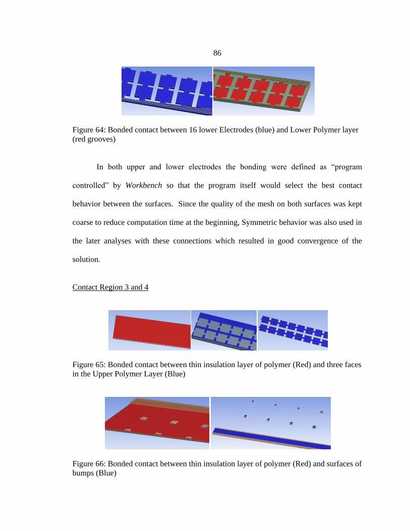
86
Figure 64: Bonded contact between 16 lower Electrodes (blue) and Lower Polymer layer
(red grooves)
In both upper and lower electrodes the bonding were defined as “program
controlled” by Workbench so that the program itself would select the best contact
behavior between the surfaces. Since the quality of the mesh on both surfaces was kept
coarse to reduce computation time at the beginning, Symmetric behavior was also used in
the later analyses with these connections which resulted in good convergence of the
solution.
Contact Region 3 and 4
Figure 65: Bonded contact between thin insulation layer of polymer (Red) and three faces
in the Upper Polymer Layer (Blue)
Figure 66: Bonded contact between thin insulation layer of polymer (Red) and surfaces of
bumps (Blue)

87
A thin insulation layer of polymer was designed in the original sensor to act as a
dielectric medium for the capacitive sensors. It was placed in between the upper and
lower electrodes where the upper electrodes as well as upper Polymer surface were in
contact with the insulation layer on one side (Figure 65 ) and the faces of the bumps
protruding from lower PDMS layer were in contact with the insulation layer on the other
side (Figure 66 ). Bonded contacts were defined in both cases of connection and the
contacts were defined as perfectly bonded so that the layers will not experience any
separation or rigid body motion within each other and the contact behavior was again
selected as program controlled by Workbench.
Contact Region 5 and 6
Since one side of the small bumps and the continuous bump was connected to the
face of thin insulation layer the other side of the bumps (blue) were assumed perfectly
bonded with lower Polymer layer (red) as shown in Figure 67. The figures are flipped to
show the mating surfaces in two different colors of blue and red respectively. Once again
the bonded behavior was left to “Program controlled”. It is safe to assume a perfect
bonding between the faces since both of the layers are made of similar type of polymers.
Figure 67: Bonded contact between lower polymer face (red) and bumps layer (blue)

88
The final contact pair was defined between the bottom surface of lower polymer
layer and the upper surface of the tibia as shown in Figure 68.
Figure 68: Frictionless contact pair between lower polymer layer (red) and tibial support
(blue) with pinball region
The lower polymer layer was resting at two end of the curved support at the two edges
about 1mm above the inner surface of the curved support. When the structure would be
under surface pressure the polymer layer is predicted to bend and began to touch the
curved surface. As a result the contact between the pair was defined as frictionless. The
rigid tibial support was defined as target surface and relatively softer lower polymer layer
was defined as contact surface. A pinball region of 0.2mm radius was defined for this
particular frictionless contact. A contact element was considered to be in near-field
contact when its integration points (gauss points or nodal points) were within a program
defined or user defined distance to the corresponding target surface and that distance was
defined as Pinball Region (36). The 0.2mm sphere was indicating the pinball region
which would start calculating for the status of contact elements of the whole polymer
contact surface (red) as soon as the sphere was about to touch the target elements. If the
radius of the pinball was set too large it would immediately start the contact algorithm

89
which would be computationally expensive since the near-field calculations (for contact
elements that were nearly or actually in contact) were usually slower and more complex
(36). The most complex calculation would begin when the contact and target elements
were actually in contact (36).
The Augmented lagrange formulation was used as the contact formulation of the
above frictionless contact and for the rest of the bonded contacts it was left as program
controlled in Workbench. These formulations were to ensure contact compatibility i.e. to
prevent the penetration of the contacting point into the target faces (37). Whenever a
contacting point penetrated a target face by an amount xn it would be pushed back by a
normal force Fn which was given by
Equation 6
Where kn is the normal stiffness having no physical meaning other than a
numerical parameter for the contact algorithm (37). Higher normal stiffness (kn) usually
results in a less penetration and vice versa (37). In Augmented Lagrange formulation an
extra term is added in the above formulation which is,
Equation 7
Where λ is the contact pressure or also known as Lagrange multiplier (37).
Whenever a contact surface is in touch with the target surface the contact pressure λ is
being calculated which prevents further penetration. This formulation is less sensitive to
normal stiffness Kn because of the contact pressure λ and suitable for general frictional or
frictionless contact in large deformation problem (37).

90
Generation of Mesh
The basic idea of finite element methods is to divide the entire geometric domain
into smaller and simpler domains which are known as finite elements (37). These
elements are connected to their neighboring elements by nodes (37). The governing
equation for each individual element can be established and solved simultaneously by the
finite element solver (37). The method of dividing a geometric model into finite number
of elements is called meshing or sometimes called finite element meshing (37).
Figure 69: SOLID186 Element type with homogeneous Structural Solid Geometry;
Image borrowed from ANSYS help documentation
Since ANSYS Workbench was used as the FEA modeler and solver it was required
to identify what type of elements Workbench generated for the 3D solid bodies. For a 3D
solid body Workbench meshes the geometry with SOLID186 elements which is a 20 node
3D second order structural solid element and it is a hexahedral in its natural shape (37)
shown in Figure 69. After deformation the element can degenerate into a triangle based
prism, quadrilateral based pyramid or tetrahedron as shown in Figure 69. If a body is
specifically meshed with SOLID187 element it is called tetrahedral dominated mesh

91
since that element is a 3D 10 node tetrahedral second order structural solid elements
which is a degenerated version of the element SOLID186 (37). Workbench has an option
to drop midside nodes of the elements which turns the edges of the elements straight (37).
Each node of The SOLID186 has three degrees of freedom which are: translations in x,y
and z directions (38). The element also supports plasticity, hyper-elasticity, creep, stress
stiffening, large deflection and large strain capabilities (38).
The half symmetric model of the sensor was meshed with a combination of
SOLID186 and SOLID187 elements in Workbench. “Body sizing” control method was
used to mesh upper and lower polymer layer and the tibial support at the bottom. An
element size of 80 microns was defined for the above mentioned meshing operation of
the solid bodies. Next another “body sizing” control of the mesh was defined for small
and solid bumps, upper and lower electrodes and the thin insulation layer of polymer. For
the bump layer the element size was defined as 20 microns and for the electrodes and
insulation layer it was defined as 50 microns and 80 microns respectively.
Figure 70 Continued: Mesh Generation

92
The mesh statistics were: total 66147 nodes and 17784 elements were generated
after the meshing operation. The whole mesh elements were a combination of
hexahedrons, tetrahedron and quadrilateral elements as shown in Figure 70. which is also
evident from the section plane cut view in the middle of the geometry in Figure 70.
Boundary Conditions and Loading Condition
Figure 71: Boundary conditions of the analysis; blue shaded zones were the fixed
supports
We assumed simplified boundary conditions for the analysis of the sensor. The
bottom of the tibia was set as fixed support as shown in Figure 71 with the blue shaded
region. Fixed support meant it was restricted to move along any direction and rotation.
Four other faces were defined as fixed support as well which were located opposite to
each other and they were along the width side of upper and lower Polymer layer. After
the boundary conditions were properly set a surface pressure was applied ranging from
1kPa to 400 kPa depending on the type of polymer material on the top surface of upper
polymer layer as indicated by the red shaded region in Figure 72.

93
Figure 72: Applying Surface Pressure on top of Polymer

94
RESULTS AND DISCUSSIONS
A varied range of pressure has been applied over the pressure sensor to observe
the structural behavior in terms of total equivalent stress, maximum principal stress,
minimum principal stress and maximum shear stress. Basically two loaded condition of
the sensor would be discussed. One would be the state where the equivalent stress stayed
below the yield point of the metal electrodes and the other state would be where the
equivalent (von-mises) stress exceeded the yield point of metal electrodes. In both cases
maximum and minimum stress level of each individual polymer layer was observed as
well to check whether they exceed their individual material yield point too.
A special failure criterion was utilized to analyze the stress developed in the
structure which was Von Mises yield criterion and its relation to the principal stresses.
Stress can be expressed as a pair of normal and shear stress (σ,Ƭ) at any arbitrary
direction. The collections of these stress pairs form a circle in the σ-Ƭ space which is
known as Mohr’s Circle which represents stress state at any given condition (37). The
point of maximum normal stress is called maximum principal stress which is located at
the right most location of the Mohr’s Circle and the point of minimum normal stress is
located at the left-most location of the Mohr’s Circle which is also known as minimum
principal stress (37). The corresponding directions are known as principal directions and
there are three principal directions and three principal stresses for a 3D solid (37). The
point of maximum and minimum shear stresses is located at the top and bottom of the
Mohr’s Circle respectively.
95
The Von Mises yield criterion is generally a commonly used failure criterion in
plasticity models for a wide range of materials (38). It is a good first approximation of
failure for metals, ductile and polymer materials. The criterion characteristic is isotropic
and independent of hydrostatic pressure, which occasionally can limit its applicability to
micro-structured materials and materials that exhibit plastic dilatation (38). Before the
criterion could be explained it is required to clarify two kinds of stress which are
hydrostatic stress and deviatoric stress. The hydrostatic stress (p) is defined as the
average of the three principal stresses where
Equation 8
And the total stress state can be written as,
Equation 9
Where the first part, σp is the hydrostatic stress and the second part, σd is called deviateric
stress which is deviating from the hydrostatic stress (37). Von-Mises proposed a theory
for predicting the failure or yielding of ductile material. The theory states that yielding
occurs when the deviatic strain energy reaches a critical value which is the yield strength
of the corresponding material (37). The criterion can be stated as: yielding occurs when
σe ≥ σy whereσe is the von Mises equivalent stress and σy is the yield strength and
corresponds to the yield in uniaxial stress loading. Equivalent stress (or von mises stress)
is related to the principal stresses by the equation:
Equation 10

96
Von Mises found that, even though none of the principal stresses exceeds the
yield stress of the material, it is possible for yielding of the material resulting from the
combination of stresses. The Von Mises criterion is a formula for combining these 3
stresses into an equivalent stress, which is then compared to the yield stress of the
material.
Finite element analyses on the sensor structure were conducted with PDMS and
Polyimide as the structural and insulation material, gold as the electrode material and a
curved solid body as the tibial support. A linear static structural analysis of the sensor
were run assuming all the material properties linear elastic since it was shown that the
material properties would stay linear within the operating pressure range of the sensor. It
was possible to get a force convergence up to 65 kPa of pressure for PDMS as structural
material. Any loading above 65kPa was resulting in a solution of non convergence for
PDMS structure. The results were tabulated in the following tables:
Table 7: Results obtained with PDMS and Gold as structural materials
Electr
ode
thickn
ess
(mm)
Electr
ode
mater
ial
Insulatio
n
Material
Appli
ed
Surfac
e
Pressu
re
(kPa)
Equival
ent
(Von-
mises)
Stress
(Mpa)
Maxim
um
Princip
al
Stress
(Mpa)
Minimu
m
Principal
Stress(M
pa)
Maxim
um
Shear
Stress
(Mpa)
Directi
onal
Deform
ation
(z-axis)
(mm)
0.02 Gold PDMS 1 75.663 75.557 14.563 38.438 0.079
0.02 Gold PDMS 5 368.63 308.13 161.74 203.64 0.2679
0.02 Gold PDMS 10 921.58 618.92 344.62 529.07 0.4428
0.02 Gold PDMS 15 1492.7 977.52 520.8 859.21 0.595
0.02 Gold PDMS 20 1997.9 1287 666.49 1151.3 0.7342
0.02 Gold PDMS 25 2461.6 1564.7 794.32 1419.3 0.8647
0.02 Gold PDMS 30 2903.2 1826.2 917.64 1674.4 0.9895
0.02 Gold PDMS 35 3126.9 1953.4 985.2 1803.7 1.0358

97
Table 7 Continued
0.02 Gold PDMS 40 3260.8 2028.2 1025.3 1881.1 1.043
0.02 Gold PDMS 45 3388.8 2099.1 1065.3 1955.1 1.049
0.02 Gold PDMS 50 3502.3 2161.9 1101.1 2020.7 1.053
0.02 Gold PDMS 55 3605.3 2219.4 1133.5 2080.2 1.058
0.02 Gold PDMS 60 3697.2 2271.1 1162.6 2133.3 1.061
0.02 Gold PDMS 65 3782 2319 1189.7 2182.3 1.065
Table 8: Results obtained with PDMS and Copper as structural materials
Electr
ode
thick
ness
(mm)
Electro
de
materi
al
Insulati
on
Materi
al
Appli
ed
Surfac
e
Pressu
re
(kPa)
Equival
ent
(Von-
mises)
Stress
(Mpa)
Maxim
um
Princip
al
Stress
(Mpa)
Minimu
m
Principal
Stress(M
pa)
Maxim
um
Shear
Stress
(Mpa)
Directi
onal
Deform
ation
(z-axis)
(mm)
0.02 Copper PDMS 1 84.322 83.288 10.893 43.263 0.067
0.02 Copper PDMS
5 357.82 324.86 151.27 200.05
0.2261
2
0.02 Copper PDMS
10 863.34 646.12 354.02 492.66
0.3743
3
0.02 Copper PDMS 15 1472 1012.9 541.88 843.82 0.5
0.02 Copper PDMS 20 2047.1 1387.4 719 1176.2 0.6159
0.02 Copper PDMS
25 2569.6 1721.2 866.18 1478.4
0.7236
4
0.02 Copper PDMS
30 3063.8 2031.5 1008.3 1764.1
0.8262
3
0.02 Copper PDMS
35 3539.1 2326.6 1147 2039
0.9253
4
0.02 Copper PDMS 40 3975.5 2594.7 1275.9 2291.4 1.0156
0.02 Copper PDMS 45 4144.3 2690.8 1332.8 2389.2 1.0342
0.02 Copper PDMS 50 4281.8 2770 1374.6 2468.8 1.0405
0.02 Copper PDMS 55 4415.4 2845.4 1416.1 2546.1 1.0463
0.02 Copper PDMS 60 4540.3 2916 1456.7 2618.4 1.0515
0.02 Copper PDMS 65 4564.8 2981.6 1494.9 2684.7 1.0569

98
Figure 73: Comparison of equivalent stress for same thickness of Gold and Copper
alternatively embedded in PDMS; electrode thickness 20 microns
Figure 74 Continued: Comparison of equivalent stress for same thickness of Gold and
Copper alternatively embedded in PDMS; electrode thickness 20 micron

99
Figure 75: Comparison of Maximum shear stress for same thickness of Gold and Copper
alternatively embedded in PDMS; electrode thickness 20 microns
Figure 76: Comparison of Maximum deflection (Z-axis) for same thickness of Gold and
Copper alternatively embedded in PDMS; electrode thickness 20 microns
100
The FEA analysis of the pressure sensor with PDMS as structural material has
been tabulated. Two different types of electrode materials were trialed: Gold and Copper,
considering the other parameters such as thickness and applied pressure being same on
each condition. The contour plots showing the deformed shape of the solid body, location
of maximum and minimum equivalent stresses, principal stresses and z-directional
deformation has been included in Appendix-A. Only z-directional deformation was
chosen to be included among the 3 directional deformations (x, y and z) since the external
transverse load was applied along that direction. If the results between Gold and Copper
as electrode material was compared it could be seen that the equivalent stress, maximum
principal stress and shear stress values remained very comparable in both cases up-to 20
kPa of applied pressure. Those stresses increased very rapidly above 20 kPa applied
pressure and significantly higher in the copper structure than gold with same thickness.
On the other hand the maximum z-directional deformation value had been always higher
in the gold embedded structure compared to copper electrodes. Finally both deflection
curve approached near each other at about 1mm deflection of the sensor as the sensor was
limited to deflect no more than 1mm due to a solid curved support of 1mm depth at the
bottom. The bottom surface of the polymer layer started to touch the tibial support at
about 35kPa with gold as the electrode material and at 40 kPa pressure it touched the
support completely with copper as electrode material embedded inside the structure
evident from Table 7 and 8, Figure 101, Appendix: A. From the material properties
defined in the earlier chapter it was visible that the stiffness of copper was 110GPa and
that of gold was 79 GPa. From the above tabulated results it could be seen that the stiffer

101
material (copper) has resulted in higher average equivalent stress inside the model of the
pressure sensor solid body and the higher stiffness has reduced the flexibility of the
sensor as evident from the reduction of z-directional deformation in case of copper. Since
the equivalent (Von-Mises) stress is a function of all three principal stresses it is easily
comprehensible that the increments of the maximum and minimum principal stresses
were also due to the added stiffness in the structure. If less equivalent stress concentration
and higher flexibility was desired then PDMS embedded with gold electrodes was the
optimum combination. The applied pressure range during the FEA analysis of the PDMS
based pressure sensor was limited to 1-65 kPa because it was really challenging to get a
force convergence above that pressure range with ANSYS Workbench analysis settings
due to PDMS stiffness being 7900 times lower than gold and 12000 times lower than that
of copper. The graphical representation of Equivalent stress vs. Applied pressure,
Maximum shear stress vs. Applied pressure, Maximum principal stress vs. Applied
pressure and Deflection vs. Applied pressure for PDMS based pressure sensor
considering both copper and gold as electrodes were shown in Figure 73, 74 and 75.
From the above tabulated data of different types of stresses developed inside the
pressure sensor with PDMS, gold and copper as structural material, the failure analysis of
the sensor was also performed. This analysis was necessary because it would forecast
whether the sensor in the above configuration would survive within the operating
pressure range and keep the structural integrity of the sensor with the selected material
types. According to Von-Mises failure criteria yielding of the structure will occur if the
equivalent stress exceeds the yield strength of the material. From the stress table above

102
and from the contour plots and color gradient of equivalent stresses and directional
deformation (Z- axis) in appendix: A, it can be seen that the color varies from blue to red
corresponding to the minimum and maximum equivalent stresses and maximum and
minimum deflection along Z-axis. The negative value of the deformation indicated a
downward deflection and positive value indicated upward deflection of the sensor along
Z- axis. By hiding some of geometry entities one by one Workbench also allowed to
inspect the location of maximum and minimum equivalent stresses developed on each
individual body parts of the solid assembly. By inserting a special ‘stress probe’ tool of
equivalent stress in the solution tree of the ANSYS Workbench, the maximum and
minimum individual stresses could be seen on each solid parts of the 3D sensor assembly.
The maximum and minimum equivalent stress results corresponding to some selected
external pressures on each component of the sensor were tabulated and given below.
Table 9: Equivalent Stress developed in Each Individual Layer: Material PDMS and Gold
(20 Microns thickness) at 1kPa
Name of
Solid Part Material
Yield
Strength
,MPa
Applied
Pressure,
kPa
Electrode
Thickness,
µm
Maximum
Equivalent
Stress
developed,
Mpa
Minimum
Equivalent
Stress
developed,
Mpa
Upper
Polymer
Layer
PDMS 2.24 1 20 5.0489e-002 2.2727e-
004
Lower
Polymer
layer
PDMS 2.24 1 20
9.4911e-002
2.8026e-
004
Upper
Electrodes
Gold 127 1 20 75.663 0.25763
Lower
Electrodes
Gold 127 1 20 48.313 0.15086
Bump PDMS 2.24 1 20 0.37722 3.429e-004

103
Layer
Insulation
Layer
PDMS 2.24 1 20 4.8612e-002 4.8612e-
002
Table 10: Equivalent Stress developed in Each Individual Layer: Material PDMS and
Gold (20 Microns thickness) at 2 kPa
Name of
Solid Part Material
Yield
Strength
,MPa
Applied
Pressure,
kPa
Electrode
Thickness,
µm
Maximum
Equivalent
Stress
developed,
Mpa
Minimum
Equivalent
Stress
developed,
Mpa
Upper
Polymer
Layer
PDMS 2.24 2 20 8.4723e-
002
4.5454e-
004
Lower
Polymer
layer
PDMS 2.24 2 20
0.15901
5.6053e-4
Upper
Electrodes
Gold 127 2 20 135.74 0.51525
Lower
Electrodes
Gold 127 2 20 104.01 0.30171
Bump
Layer
PDMS 2.24 2 20 0.73982 6.858e-
004
Insulation
Layer
PDMS 2.24 2 20 0.10297 2.1538e-
004
Table 11: Equivalent Stress developed in Each Individual Layer: Material PDMS and
Gold (20 Microns thickness) at 3 kPa
Name of
Solid Part Material
Yield
Strength
,MPa
Applied
Pressure,
kPa
Electrode
Thickness,
µm
Maximum
Equivalent
Stress
developed,
Mpa
Minimum
Equivalent
Stress
developed,
Mpa
Upper
Polymer
Layer
PDMS 2.24 3 20 0.11254 6.7578e-
004
Lower
Polymer
layer
PDMS 2.24 3 20
0.1982
8.3336e-
004
Upper Gold 127 3 20 204.44 0.76605
Table 9 Continued

104
Electrodes
Lower
Electrodes
Gold 127 3 20 168.16 0.44857
Bump
Layer
PDMS 2.24 3 20 1.123 1.0196e-
003
Insulation
Layer
PDMS 2.24 3 20 0.14924 3.2022e-
004
Table 12: Equivalent Stress developed in Each Individual Layer: Material PDMS and
Gold (20 Microns thickness) at 7 kPa
Name of
Solid Part
Material Yield
Strength
,MPa
Applied
Pressure,
kPa
Electrode
Thickness,
µm
Maximum
Equivalent
Stress
developed,
Mpa
Minimum
Equivalent
Stress
developed,
Mpa
Upper
Polymer
Layer
PDMS 2.24 7 20 0.19877 1.4812e-3
Lower
Polymer
layer
PDMS 2.24 7 20
0.29217
1.8266e-
003
Upper
Electrodes
Gold 127 7 20 566.72 1.679
Lower
Electrodes
Gold 127 7 20 426.44 0.98318
Bump
Layer
PDMS 2.24 7 20 2.5518 2.2348e-
003
Insulation
Layer
PDMS 2.24 7 20 0.29476 7.0185e-
004
Table 13: Equivalent Stress developed in Each Individual Layer: Material PDMS and
Gold (20 Microns thickness) at 65 kPa
Name of
Solid Part
Material Yield
Strength
,MPa
Applied
Pressure,
kPa
Electrode
Thickness,
µm
Maximum
Equivalent
Stress
developed,
Mpa
Minimum
Equivalent
Stress
developed,
Mpa
Upper
Polymer
Layer
PDMS 2.24 65 20 0.484 1.0028e-
002
Table 11 Continued

105
Lower
Polymer
layer
PDMS 2.24 65 20
0.7972
2.1387e-
002
Upper
Electrodes
Gold 127 65 20 3782 13.657
Lower
Electrodes
Gold 127 65 20 1768.8 9.7333
Bump
Layer
PDMS 2.24 65 20 13.529 6.3054e-
002
Insulation
Layer
PDMS 2.24 65 20 0.76477 8.1028e-
003
From the Table 9, it was clearly evident that at 1 kPa pressure the equivalent
stress generated at each individual layer of the sensor stayed below their corresponding
yield strength of the constituent materials. The components would undergo only linear
elastic deformation and the stress was within their elastic limit at that pressure. However
at 2 kPa pressure from Table 10, the equivalent stress developed in the upper gold
electrodes of 20 micron thickness slightly exceeded the yield strength of the material
which might led to plastic deformation (Figure 102, Appendix A) at some of the points.
That means some part of upper electrodes would experience permanent deformation
without returning to its original state. The other part of the sensor stayed below their
corresponding yield point. At 3 kPa pressure both upper and lower electrodes of gold
material experienced plastic deformation and yielding since the equivalent stress at
certain points of their structure exceeded the yield strength (Figure 103, Appendix A).
The stress built up in the PDMS encapsulation at this pressure range was also significant
in this case but it was below its yield point. At 7 kPa external pressure the equivalent
stress developed in the bumps reached to a value of 2.55 MPa which was slightly higher
than the yield strength of PDMS. This was the first time when the PDMS made bump
Table 13 Continued
106
structures was experiencing plastic deformation (Figure 104, Appendix A) inside the
sensor and these bumps were suffering from some degree of permanent deformation once
the sensor was subjected to that amount of external pressure. Instead of elastic recovery
of the bumps some of them will be plastically deformed after the sensor will be used for
measurement of pressure distribution inside the knee joint. The other PDMS made bodies
like upper and lower polymer layer and thin insulation layer experienced a very small
amount of equivalent stress which was well below the yield point of PDMS as shown in
the above Table 9,10 11,12 and 13.
Similarly PDMS with copper as electrode material with same thickness similar to
gold electrodes underwent plastic deformation at about 4 kPa external pressure. An
equivalent stress of 271.96 MPa was developed at upper copper electrodes which
exceeded the yield strength of copper of 252.3 MPa. The lower electrodes experienced a
maximum equivalent stress of 228.33 MPa which was still less than its yield point. The
yielding continued as the pressure was increased subsequently over the pressure sensor.
At 7 kPa pressure the PDMS made bumps started to experience plastic deformation
because the equivalent stress of 2.25 MPa just exceeded its yield strength.
It was possible to get a force convergence with PDMS and Gold as sensor
materials up-to 65 KPa and the PDMS made upper and lower encapsulation layers still
remained linear elastic at that pressure range. Among the PDMS layers the lower polymer
layer experienced the highest equivalent stress of 0.7972 MPa shown in Table 13 for 65
kPa of applied pressure which is still much lower than the yield stress of 2.24 MPa for

107
PDMS. The thin insulation layer developed the maximum equivalent stress of 0.829 MPa
when copper was used as electrodes.
Another iteration of FEA analyses were ran with the same geometrical
configuration but this time it was Polyimide as the structural and insulation material.
Both gold and copper were considered as electrode material in the analyses. For
Polyimide the force convergence pressure range achieved was much higher compared to
PDMS. The analyses were run in between 10-100 kPa range at an increment of 10 kPa
and from 100-400 kPa at an increment of 50 kPa. The results are tabulated below:
Table 14: Results obtained with Polyimide and Gold as structural materials
Electr
ode
thickn
ess
(mm)
Elect
rode
mate
rial
Insulatio
n
Material
Appl
ied
Surf
ace
Pres
sure
(kPa
)
Equival
ent
(Von-
mises)
Stress
(Mpa)
Maxim
um
Princip
al
Stress
(Mpa)
Minimu
m
Principa
l
Stress(
Mpa)
Maxi
mum
Shear
Stress
(Mpa)
Directi
onal
Deform
ation
(z-axis)
(mm)
0.02
Gold Polyimi
de 10 12.856 13.122 1.1597 6.4671 0.0056
0.02 Gold Polyimi
de 20 25.229 25.744 21.363 12.69 0.011
0.02 Gold Polyimi
de 30 37.186 37.937 3.3864 18.702 0.0163
0.02 Gold Polyimi
de 40 48.831 49.81 4.4608 24.557
0.0214
1
0.02 Gold Polyimi
de 50 60.076 61.279 5.5075 30.211
0.0263
2
0.02 Gold Polyimi
de 60 70.947 72.368 6.5335 36.461
0.0310
5
0.02 Gold Polyimi
de 70 81.701 83.11 8.5205 45.996
0.0356
16
0.02 Gold Polyimi
de 80 98.843 93.561 11.526 55.558 0.04
0.02 Gold Polyimi 90 115.89 103.81 14.658 65.956 0.0444

108
de
0.02 Gold Polyimi
de 100 137.32 113.88 17.874 79.023
0.0486
6
0.02 Gold Polyimi
de 150 261.81 162.53 33.584 151.05
0.0692
13
0.02 Gold Polyimi
de 200 385.52 208.5 47.319 222.55 0.089
0.02 Gold Polyimi
de 250 501.02 264.67 58.322 289.25
0.1081
2
0.02 Gold Polyimi
de 300 612.76 319.51 69.339 353.77 0.1267
0.02 Gold Polyimi
de 350 721.49 373.11 78.89 416.54
0.1456
1
0.02 Gold Polyimi
de 400 827.46 425.4 89.336 477.73 0.164
Table 15: Results obtained with Polyimide and Copper as structural materials
Electr
ode
thick
ness
(mm)
Electro
de
materi
al
Insulatio
n
Material
Appl
ied
Surf
ace
Pres
sure
(kPa
)
Equival
ent
(Von-
mises)
Stress
(Mpa)
Maxim
um
Princip
al
Stress
(Mpa)
Minim
um
Princip
al
Stress(
Mpa)
Maxim
um
Shear
Stress
(Mpa)
Directio
nal
Deforma
tion (z-
axis)
(mm)
0.02
Coppe
r
Polyimi
de 10 16.26 16.497 1.1576 8.1737
0.00551
7
0.02 Coppe
r
Polyimi
de 20 31.953 32.417 2.2838 16.061
0.01088
7
0.02 Coppe
r
Polyimi
de 30 47.151 47.832 3.3818 23.7
0.01611
1
0.02 Coppe
r
Polyimi
de 40 61.996 62.89 4.4556 31.16 0.02118
0.02 Coppe
r
Polyimi
de 50 76.363 77.468 5.5 38.378 0.026
0.02 Coppe
r
Polyimi
de 60 90.172 91.484 6.522 45.319 0.03
0.02 Coppe
r
Polyimi
de 70 103.53 105.04 7.9971 52.033 0.0352
0.02 Coppe
r
Polyimi
de 80 116.57 118.28 10.904 58.589 0.04
0.02 Coppe Polyimi 90 129.38 131.29 13.943 65.028 0.04383
Table 14 Continued

109
r de 9
0.02 Coppe
r
Polyimi
de 100 141.98 144.08 17.072 75.906
0.04803
8
0.02 Coppe
r
Polyimi
de 150 253.39 206.08 32.576 146.18 0.0683
0.02 Coppe
r
Polyimi
de 200 375.71 265.24 46.352 216.88 0.0877
0.02 Coppe
r
Polyimi
de 250 490 321.93 57.432 282.88 0.10673
0.02 Coppe
r
Polyimi
de 300 600.42 378.06 68.331 346.64 0.12536
0.02 Coppe
r
Polyimi
de 350 708.04 433.79 77.977 408.78 0.14376
0.02 Coppe
r
Polyimi
de 400 812.41 489.13 87.859 469.04 0.16194
Figure 77: Comparison of equivalent stress for same thickness of Gold and Copper
alternatively embedded in Polyimide; electrode thickness 20 microns
Table 15 Continued
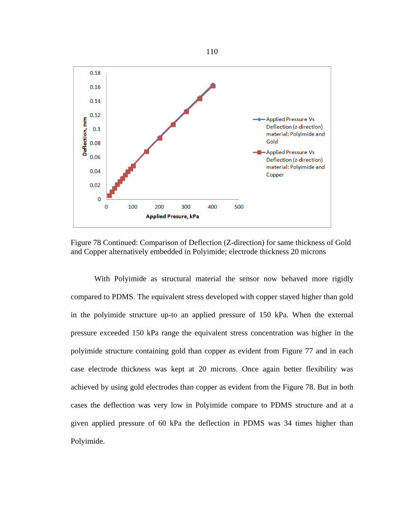
110
Figure 78 Continued: Comparison of Deflection (Z-direction) for same thickness of Gold
and Copper alternatively embedded in Polyimide; electrode thickness 20 microns
With Polyimide as structural material the sensor now behaved more rigidly
compared to PDMS. The equivalent stress developed with copper stayed higher than gold
in the polyimide structure up-to an applied pressure of 150 kPa. When the external
pressure exceeded 150 kPa range the equivalent stress concentration was higher in the
polyimide structure containing gold than copper as evident from Figure 77 and in each
case electrode thickness was kept at 20 microns. Once again better flexibility was
achieved by using gold electrodes than copper as evident from the Figure 78. But in both
cases the deflection was very low in Polyimide compare to PDMS structure and at a
given applied pressure of 60 kPa the deflection in PDMS was 34 times higher than
Polyimide.

111
Table 16: Equivalent Stress developed in Each Individual Layer: Material Polyimide and
Gold (20 Microns thickness) at 100 kPa
Name of
Solid Part
Material Yield
Strength
,MPa
Applied
Pressure,
kPa
Electrode
Thickness,
µm
Maximum
Equivalent
Stress
developed,
Mpa
Minimum
Equivalent
Stress
developed
, Mpa
Upper
Polymer
Layer
Polyimid
e
231 140 20 24.788 9.8731e-
002
Lower
Polymer
layer
Polyimid
e
231 140 20 93.356
0.23439
Upper
Electrodes
Gold 127 140 20 115.61 0.4108
Lower
Electrodes
Gold 127 140 20 149.97 0.45375
Bump Layer Polyimide 231 140 20 236.12 7.108e-2
Table 16 Continued
Insulation
Layer
Polyimid
e
231 140 20 20.244 4.202e-
002
The equivalent stress developed in the polyimide structures were not significant
until 140 kPa external pressure was applied shown at Table 16. At that pressure the stress
concentration at some point of the polyimide bumps and lower gold electrodes were high
enough to surpass their yield strengths and caused plastic deformation. The contour plot
of the locations of the plastic deformations was given at Figure 105, Appendix: A. and at
170 kPa pressure the upper electrodes also started to plastically deform inside Polyimide-
Gold structure by 136.26 MPa of equivalent stress which surpassed its yield point of 127
Mpa shown in Figure 106, Appendix: A. Similarly In Polyimide-Copper Structure, the
Polyimide bumps and Lower electrodes started to undergo plastic deformation at 137 kPa
pressure and lower copper electrodes experienced the yielding at about

112
Thickness Effect
FEA analyses were run again on polyimide structure to observe the thickness
effect of metal electrodes. Two different thicknesses of metal electrodes were compared
which were 5 and 20 microns embedded inside the same thickness of Polyimide to
observe the effect. The results are tabulated below:
Table 17: Results obtained with Polyimide and Gold (thickness of 5 microns) as
structural materials
Electr
ode
thickn
ess
(mm)
Electro
de
materia
l
Insulatio
n
Material
Appl
ied
Surf
ace
Press
ure
(kPa
)
Equival
ent
(Von-
mises)
Stress
(Mpa)
Maxim
um
Princip
al
Stress
(Mpa)
Minimu
m
Princip
al
Stress(
Mpa)
Maxim
um
Shear
Stress
(Mpa)
Directio
nal
Deforma
tion (z-
axis)
(mm)
0.005
Gold Polyimid
e 10 17.633 15.149 1.5621 9.0576
0.00627
17
0.005 Gold Polyimid
e 20 32.33 28.218 2.9356 16.632 0.0121
0.005 Gold Polyimid
e 30 44.576 39.394 4.1322 22.971
0.01752
1
0.005 Gold Polyimid
e 40 54.657 48.765 5.1077 28.215 0.0225
0.005 Gold Polyimid
e 50 63.329 56.954 5.98 32.745
0.02721
6
0.005 Gold Polyimid
e 60 72.352 64.085 7.0794 41.003 0.0317
0.005 Gold Polyimid
e 70 89.906 69.671 8.9931 50.951 0.03601
0.005 Gold Polyimid
e 80 107.39 75.817 11.965 60.865 0.04
0.005 Gold Polyimid
e 90 124.73 88.4 14.974 70.708 0.04433
0.005 Gold Polyimid
e 100 144.58 100.75 18.067 83.159 0.04838
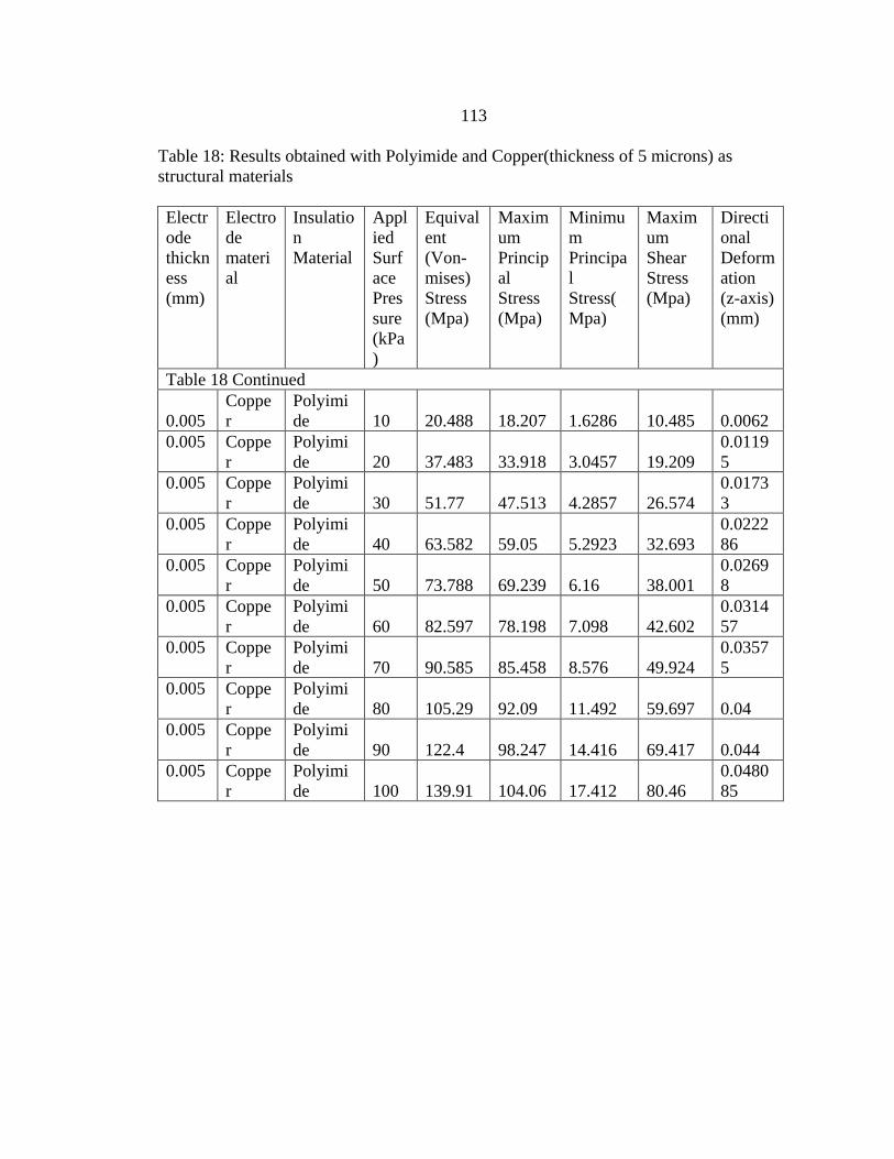
113
Table 18: Results obtained with Polyimide and Copper(thickness of 5 microns) as
structural materials
Electr
ode
thickn
ess
(mm)
Electro
de
materi
al
Insulatio
n
Material
Appl
ied
Surf
ace
Pres
sure
(kPa
)
Equival
ent
(Von-
mises)
Stress
(Mpa)
Maxim
um
Princip
al
Stress
(Mpa)
Minimu
m
Principa
l
Stress(
Mpa)
Maxim
um
Shear
Stress
(Mpa)
Directi
onal
Deform
ation
(z-axis)
(mm)
Table 18 Continued
0.005
Coppe
r
Polyimi
de 10 20.488 18.207 1.6286 10.485 0.0062
0.005 Coppe
r
Polyimi
de 20 37.483 33.918 3.0457 19.209
0.0119
5
0.005 Coppe
r
Polyimi
de 30 51.77 47.513 4.2857 26.574
0.0173
3
0.005 Coppe
r
Polyimi
de 40 63.582 59.05 5.2923 32.693
0.0222
86
0.005 Coppe
r
Polyimi
de 50 73.788 69.239 6.16 38.001
0.0269
8
0.005 Coppe
r
Polyimi
de 60 82.597 78.198 7.098 42.602
0.0314
57
0.005 Coppe
r
Polyimi
de 70 90.585 85.458 8.576 49.924
0.0357
5
0.005 Coppe
r
Polyimi
de 80 105.29 92.09 11.492 59.697 0.04
0.005 Coppe
r
Polyimi
de 90 122.4 98.247 14.416 69.417 0.044
0.005 Coppe
r
Polyimi
de 100 139.91 104.06 17.412 80.46
0.0480
85

114
Figure 79: Equivalent Stress in the Polyimide Structure considering Gold Electrodes of 5
and 20 microns thickness alternatively
Figure 80: Deflection (Z-directional) in the Polyimide Structure considering Gold
Electrodes of 5 and 20 microns thickness alternatively

115
Figure 81: Equivalent Stress in the Polyimide Structure considering Copper
Electrodes of 5 and 20 microns thickness alternatively
Figure 82: Deflection (Z-directional) in the Polyimide Structure considering Copper
Electrodes of 5 and 20 microns thickness alternatively

116
Figure 83: Comparison of Equivalent Stress in the Polyimide Structure
considering both Copper and Gold Electrodes of 5 microns thickness
From the above graphical representation it was clearly evident that lower
thickness of gold electrodes produced more stress concentration in the polyimide
structure than the higher thickness of the same material shown in Figure 79. On the other
hand the thinner metal film of gold resulted in more deflection or flexibility in the
structure than thicker film shown in Figure 80. However the thickness variation of copper
as electrode material exhibited somewhat different behavior than gold material. The
lower thickness of copper electrodes produced higher stress concentration in the
polyimide structure upto 50 kPa of applied pressure but the stress concentration went
down compared to higher thickness of copper electrodes after 50 kPa applied pressure as
shown in Figure 81. So in case of copper material, higher thickness of electrodes would
be beneficial upto a low range of applied pressure (1-50kPa). As the contact stress would
rise, thinner copper electrodes would produce less stress concentration in the structure.

117
The deflection characteristics curve with copper was found similar as gold shown in
Figure 82. Overall gold as electrodes material would produce lesser stress concentration
in the polyimide structure than copper of similar thickness evident from Figure 83 due to
copper stiffness being 1.4 times higher than gold material.
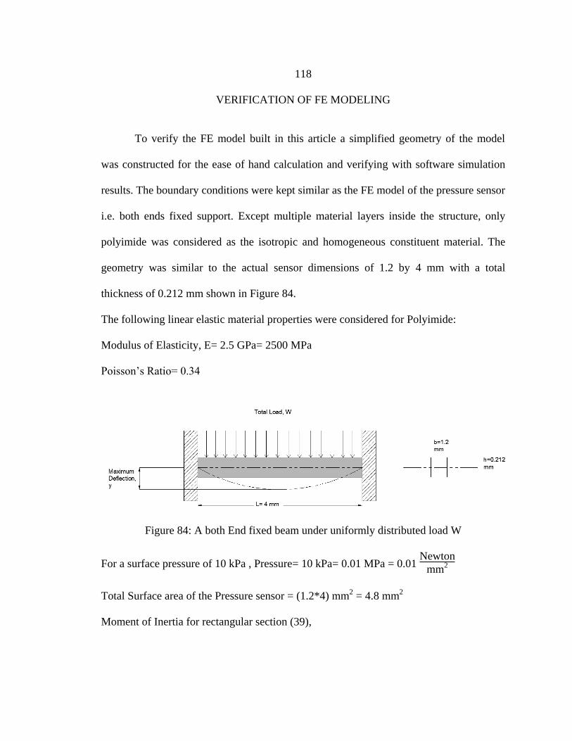
118
VERIFICATION OF FE MODELING
To verify the FE model built in this article a simplified geometry of the model
was constructed for the ease of hand calculation and verifying with software simulation
results. The boundary conditions were kept similar as the FE model of the pressure sensor
i.e. both ends fixed support. Except multiple material layers inside the structure, only
polyimide was considered as the isotropic and homogeneous constituent material. The
geometry was similar to the actual sensor dimensions of 1.2 by 4 mm with a total
thickness of 0.212 mm shown in Figure 84.
The following linear elastic material properties were considered for Polyimide:
Modulus of Elasticity, E= 2.5 GPa= 2500 MPa
Poisson’s Ratio= 0.34
Figure 84: A both End fixed beam under uniformly distributed load W
For a surface pressure of 10 kPa , Pressure= 10 kPa= 0.01 MPa = 0.01 Newton
mm2
Total Surface area of the Pressure sensor = (1.2*4) mm2 = 4.8 mm
2
Moment of Inertia for rectangular section (39),

119
Equation 11
= 1.2 mm*0.2123mm
3
12
= 9.528E-4 mm4
Section modulus of Cross section of beam (39),
Equation 12
= 1.2mm*0.2122mm
2
6
=0.00898 mm3
So, total surface load, W= Total Surface Pressure * Total Surface Area
= (0.01*4.8) (mm2 * Newton/mm
2)
= 0.048 Newton
For a Both End Fixed beam, maximum deflection equation from (40) for a 0.048 Newton
force will be,
Equation 13
=0.048 Newton*(4)
3mm
3
384*2500(Newton/mm2)*(9.528E-4mm
4)
= 0.003358 mm
Maximum Stress at fixed ends (40),
Equation 14
= 0.048 Newton*4mm
12*0.00898 mm3
= 1.7817 MPa

120
Workbench Simulation Results for both end Fixed beam:
Figure 85: Both end Fixed Polyimide beam with surface pressure of 10 kPa
Figure 86: Location of Maximum Stress at Fixed end and Maximum downward
deflection at 10 kPa pressure
From Workbench simulation a maximum z directional deflection derived for 10
kPa pressure was 0.00338mm and hand calculated maximum deflection value derived
from Equation 13 was 0.003358mm with a percentage error of 0.65% between them.
Value of Maximum stress found at the fixed ends by hand calculation using Equation 14
was 1.78 MPa and maximum equivalent stress from Workbench simulation was 1.771
MPa shown in Figure 86 with a percentage error of 0.5% between them.
So from the above evaluation it would be safe to assume that the Finite element
model of the pressure sensor were relevant and verified simulation results.

121
THERMAL STRESS
Thermal stresses are induced in microsystems operating at higher temperature due
to mechanical constraints or mismatch of coefficient of thermal expansion of the mating
parts. Since most microdevices are made of components having different materials such
as deposited thin films, so mismatch of coefficient of thermal expansion (CTE) should be
considered during the design process since excessive stress could be a cause of the failure
of the device (5).
Since the temperature during Electrochemical deposition range from room
temperature to 1000C (42) so due to mismatch of coefficient of thermal expansion for
metal and polymer materials some thermal stress will develop in the structure when they
will be cooled down to room temperature due to contraction. A 2D analysis of the sensor
structure was performed considering both PDMS and Polyimide as polymer membrane
alternatively and trialed both gold and copper as electrode material to verify if the stress
developed due to difference of CTE was significant enough or not. The analysis would
only be applicable if the polymer casting over silicon wafer started immediately after the
metallization process so that it would result in good adhesion between polymer and metal
layer. If the casting of polymer was performed after the metal layer cooled down to room
temperature than this analysis would not be significant. The temperature difference would
induce thermal load inside the structure and produce residual thermal stress when cooled
down to room temperature. Our point of interest was to verify if the residual stress would
create any plastic deformation in the structure.

122
The thermal material properties used were:
Coefficient of thermal expansion of PDMS = 310E-6 1
Kelvin (26)
Coefficient of thermal expansion of Polyimide = 20E-6 1
Kelvin (32)
Coefficient of thermal expansion of Gold = 14.2E-6 1
Kelvin (33)
Coefficient of thermal expansion of Copper = 17E-6 1
Kelvin (44)
In the simulation the model was cooled down from 1000C to room temperature of 220C
and the effect was observed if the cooling process induced any residual stress inside the
structure. The analysis was performed using ANSYS parametric design language (APDL)
and the code was included in the appendix B section. The results are tabulated below:
Table 19: Total Equivalent stress and Total thermal and mechanical Strain Considering
different materials
Material
Total
Maximum
Equivalent
Stress
Developed,
MPa
Total
Minimum
Equivalent
Stress
Developed,
MPa
Total
Maximum
Mechanical
and
Thermal
Strain
Total
Minimum
Mechanical
and
Thermal
Strain
PDMS
and Gold
0.338435 0.579E-05 0.094743 0.342E-07
PDMS
and
Copper
0.334705 0.572E-05 0.095092 0.231E-07
Polyimide
and Gold
18.7359 0.406E-03 0.007494 0.162E-06
Polyimide
and
Copper
19.5259 0.334E-03 0.00781 0.134E-06
123
From the above results of Table 19 for only thermally applied load on a 2D sensor
model it could be observed that a maximum residual stress of 0.338 MPa and 0.334 MPa
were developed at the interface of PDMS with gold/copper layers alternatively shown in
Figure 107 and 109, Appendix A. Similarly A maximum equivalent stress of 18.7359
MPa and 19.5259 MPa were developed with polyimide and gold/copper interface shown
in Figure 111 and 113, Appendix A. PDMS structure underwent about 12 times more
thermal and mechanical strain compared to polyimide shown in Figure 108 and 110,
Appendix A. It was due to PDMS having very large coefficient of thermal
expansion/contraction which was 16 times higher than that of Polyimide and mechanical
stiffness was much higher in Polyimide. PDMS structure containing gold electrodes had
very comparable residual stress with PDMS containing copper electrodes which were due
to the fact that gold and copper had very similar coefficient of thermal expansion. As a
result the residual stress was largely dominated by contraction of the PDMS membrane
and it was well below yield stress of any of the constituent material. Similarly the
residual stress in the polyimide structure was also below yield limit of any of the
constituent material but releasing the stress would be a better solution to confirm
accuracy and precision of reading form the sensor.

124
READOUT CIRCUIT SCHEMATIC
Any typical capacitance readout circuit consists of a scanning circuitry in the form
of row and column decoder or a set of multiplexers providing the driving signals (Source
voltage) to either row or column electrodes. For a target sensing element (Cs), a
sinusoidal input voltage (Vs) would be applied to the capacitor and corresponding output
voltage Vowould be measured by the relation:
Equation 15
Where Cf is the feedback capacitance and Rf is the feedback resistance shown in Figure
87. When the sinusoidal input voltage Vswould be switched to the pressure sensing
capacitive cell element by row/column multiplexer sub-circuits, the electric charge stored
in the capacitance due to polymer surface deflection would be transferred to the
capacitance measurement circuit feedback capacitance Cf which would be converted into
a DC signal Vo as given by Equation 15 by a peak value detector and detected by analog-
to-digital converter (ADC). A data acquisition system on a chip would be used as
controller of the scanning circuit. Two multiplexer would require for selecting row and
column electrodes and an operational amplifier (Op amp) would be used for signal
conditioning. Scanning request could be made from a computer through universal serial
bus or parallel port interface and scanned data could be transferred back to the computer
again for visualization and data analysis purpose shown in the schematic diagram in
Figure 88.

125
Figure 87: Typical Read-Out Circuit for Capacitive sensor
Figure 88: Capacitive Row and Column Senor Array with Scanning Circuits using
Multiplexers; R 1, R2.. R16 and C1, C2.. C16 represents Row and Column respectively;
Image and Idea inspired from (41)
126
FUTURE WORK AND CONCLUSION
There is still a lot of improvement scope for this work. The future work of this
pressure sensor would be to go for the actual clean-room fabrication of the sensor. Once
the constituent materials and designs would be finalized a distinct and precise fabrication
steps would reduce the cost and raise the efficiency of the fabrication greatly. The current
design would allow fabricating two sensors at a time within a single silicon wafer with
same process steps and materials but minor tweaking in the design might allow more to
fabricate at a time. Because these silicon micro-fabrication process requires multiple
attempts to achieve a successful product on a trial and error basis. An extensive research
need to be made on the bonding techniques and success of different materials to avoid
delamination of different layers during the actual fabrication of the sensor. This work was
an effort to start the design of this unique pressure sensor from scratch and highlight
various design aspects of the sensor model from electromechanical and structural
perspective. Since it was a micro-electro mechanical device a solid readout circuit design
with high gain and signal to noise ratio would be paramount for accurate and precise
reading from the sensor. Construction of such a precise circuit would be challenging but
possible since there have been many sensitive readout circuits already made for
capacitance measurements found in various relevant literatures. Calibration of the sensor
would be of utmost importance because in order to have a functional pressure sensor and
to get readings from it, the sensor should be properly calibrated. Micro force gauge with
force transducers could be utilized in calibration of this type sensor by pressing the force
probe against each sensitive cell and plotting the response Vs force graph.
127
This pressure sensor was intended to be used inside a mouse knee and there had
been no such pressure sensor array fabricated yet to measure contact stress distribution of
geometry in such a small scale. There had been some attempt made to prototype the
sensor with flexible printed circuits on kapton polymer (polyimide) but the minimum
feature size achievable by flexible Circuit board printing didn’t meet the requirements of
minimum feature size for our specific requirement. The flexible PCB printing required
reducing the number of sensing elements from the sensor to prototype which would
greatly reduce sensitivity and pressure mapping area inside knee joint. So the best
solution would be to invest in a clean-room micro-fabrication of the pressure sensor
where submicron feature sizes would be possible to make with greater precision on a
silicon wafer.

128
REFERENCES CITED

129
1. Ko WH, Min-Hang B, Yeun-Ding H, editors. A high-sensitivity integrated-circuit
capacitive pressure transducer1982: IEEE.
2. Narducci M, Yu-Chia L, Fang W, Tsai J. CMOS MEMS capacitive absolute pressure
sensor. JOURNAL OF MICROMECHANICS AND MICROENGINEERING.
2013;23(5).
3. Goldring MB, Goldring SR. Osteoarthritis. Journal of cellular physiology.
2007;213(3):626-34.
4. Segal NA, Anderson DD, Iyer KS, Baker J, Torner JC, Lynch JA, et al. Baseline
articular contact stress levels predict incident symptomatic knee osteoarthritis
development in the MOST cohort. Journal of orthopaedic research : official publication
of the Orthopaedic Research Society. 2009;27(12):1562-8.
5. MEMS and MICROSYSTEMS, 2nd Edition by Tai-Ran Hsu
6. Eaton WP, Smith JH. Micromachined pressure sensors: review and recent
developments. Smart Materials and Structures. 1997;6(5):530-9.
7. A. Heidary, "A Low-Cost Universal Integrated Interface for Capacitive
Sensors"promotor: prof.dr.ir. G.C.M. Meijer;2010, 150p. ISBN: 978-94-6113-
8. Hunter DJ. Osteoarthritis. Best practice & research Clinical rheumatology.
2011;25(6):801-14.
9. Vincent C. Hascall, Klaus E. Kuettner. The many faces of Osteoarthritis, Pg-383
10. Leena Sharma, Francis Berenbaum. A Companion to Rheumatology Osteoarthritis.
11. Segal NA, Kern AM, Anderson DD, Niu J, Lynch J, Guermazi A, et al. Elevated
tibiofemoral articular contact stress predicts risk for bone marrow lesions and cartilage
damage at 30 months. Osteoarthritis and cartilage / OARS, Osteoarthritis Research
Society. 2012;20(10):1120-6.
12. Teeple E, Jay GD, Elsaid KA, Fleming BC. Animal Models of Osteoarthritis:
Challenges of Model Selection and Analysis. The AAPS Journal. 2013;15(2):438-46.
13. Kamekura S, Nakamura K, Kawaguchi H, Hoshi K, Shimoaka T, Chung U, et al.
Osteoarthritis development in novel experimental mouse models induced by knee joint
instability. Osteoarthritis and cartilage / OARS, Osteoarthritis Research Society.
2005;13(7):632-41.
130
14. Rose T.J, MSME Thesis, “Static Loading Apparatus for Mouse and Rat Knees” May
2013
15. Goldring MB. Do mouse models reflect the diversity of osteoarthritis in humans?
Arthritis and rheumatism. 2012;64(10):3072-5.
16. Hyung-Kew L, Sun-Il C, Yoon E, Yoon E. A Flexible Polymer Tactile Sensor:
Fabrication and Modular Expandability for Large Area Deployment. Journal of
Microelectromechanical Systems. 2006;15(6):1681-6.
17. Dagamseh AMK, Wiegerink RJ, Lammerink TSJ, Krijnen GJM.Towards a high-
resolution flow camera using artificial hair sensor arrays for flow pattern
observations.Bioinspiration&biomimetics. 2012;7(4):046009.
18. Cheng MY, Huang XH, Ma CW, Yang YJ. A flexible capacitive tactile sensing array
with floating electrodes.Journal of Micromechanics and Microengineering.
2009;19(11):115001.
19.http://www.amicusvisualsolutions.com/cgibin/big_image.cgi?image=05009_01X&ori
entation=H. [Online]
20. Introduction to Microelectronic Fabrication, 2nd Edition by Richard C. Jaeger
21. Bean KE, Bean KE. Anisotropic etching of silicon. IEEE Transactions on Electron
Devices. 1978;25(10):1185-93.
22. Schneider F, Draheim J, Kamberger R, Wallrabe U. Process and material properties
of polydimethylsiloxane (PDMS) for Optical MEMS. Sensors & Actuators: A Physical.
2009;151(2):95-9
23. Satoshi S, Sawano S, Keisuke N, Naka K, Werber A, Werber A, et al., editors.
Sealing method of PDMS as elastic material for MEMS2008: IEEE.
24. Larsen AL, Hansen K, Sommer-Larsen P, Hassager O, Bach A, Ndoni S, et al. Elastic
properties of nonstoichiometric reacted PDMS networks. MACROMOLECULES.
2003;36(26):10063-70.
25. Lei KF, Lee KF, Lee MY. Development of a flexible PDMS capacitive pressure
sensor for plantar pressure measurement. MICROELECTRONIC ENGINEERING.
2012;99:1-5.
26. http://www.mit.edu/~6.777/matprops/pdms.htm [Online]

131
27. Hasenkamp W, Forchelet D, Pataky K, Villard J, Lintel HV, Bertsch A, et al.
Polyimide/SU-8 catheter-tip MEMS gauge pressure sensor. Biomedical Microdevices.
2012;14(5):819-28.
28. Hubbard RL, Fathi Z, Ahmad I, Matsutani H, Hattori T, editors. Low temperature
curing of polyimide wafer coatings2004.
29. Damaceanu MD, Rusu RD, Bruma M, Muller A, editors. Thin polyimide films for
dielectric interlayer application2009.
30. http://www.arl.army.mil/arlreports/2009/ARL-TR-5031.pdf [Online]
31.http://www2.dupont.com/Kapton/en_US/assets/downloads/pdf/summaryofprop.pdf
[Online]
32. http://www2.dupont.com/Packaging_and_Circuits/en_US/assets/downloads/pdf/HD-
7000_ProcessGuide.pdf [Online]
33. http://www.mit.edu/~6.777/matprops/gold.htm [Online]
34. Xiang Y, Tsui TY, Vlassak JJ. The mechanical properties of freestanding
electroplated Cu thin films. JOURNAL OF MATERIALS RESEARCH.
2006;21(6):1607-18.
35. Ding M, Dalstra M, Linde F, Hvid I. Mechanical properties of the normal human
tibial cartilage-bone complex in relation to age. Clinical Biomechanics. 1998;13(4):351-
8.
36. http://www1.ANSYS.com/customer/content/documentation/120/ans_ctec.pdf [Online]
37. “Finite Element Simulation with ANSYS Workbench 13” by Huei-Huang Lee
38. ANSYS. Documentation for ANSYS Workbench
39. “Vector Mechanics for Engineers”, 9th Edition by Beer,Johnston et al.
40. Machinery’s Handbook, 28th Edition by Oberg E, Jones F. et al. 2008.
41.Cheng M-Y, Lin C-L, Lai Y-T, Yang Y-J. A polymer-based capacitive sensing array
for normal and shear force measurement. Sensors (Basel, Switzerland).
2010;10(11):10211-25.
42. “Introduction to Microfabrication” By Sami Franssila

132
43. Van den Noort JJC, van der Esch M, Steultjens MPM, Dekker J, Schepers MHM,
Veltink PH, et al. Ambulatory measurement of the knee adduction moment in patients
with osteoarthritis of the knee. Journal of biomechanics. 2013;46(1):43-9.
44. Thermal Expansion. Wikipedia. [Online]
http://en.wikipedia.org/wiki/Thermal_expansion.

133
APPENDICES

134
APPENDIX A:
CONTOUR PLOTS

135
For all images with Isometric view, the following axis orientations were used:
Figure 89: Equivalent (Von-mises) stress and directional deformation at any point in the
structure at 1 kPa pressure; material PDMS and Gold

136
Figure 90: At 1 kPa,Von-mises Stress distribution on Upper and lower electrodes and
location of max stress; material PDMS and Gold
Figure 91: At 1 kPa ,Maximum Principal Stress on Upper and lower electrodes and
location of max stress; material PDMS and Gold

137
Figure 92: At 10kPa, Equivalent (Von-mises) stress and z-deformation at any point in the
structure at 10KPa pressure; material PDMS and Gold
Figure 93: At 10 kPa,Stress distribution on Upper and lower electrodes and location max
stress; material PDMS and Gold

138
Figure 94: At 20KPa Equivalent (Von-mises) stress and z-directional deformation at any
point in the structure at 20kPa pressure; material PDMS and Gold
Figure 95: At 20 kPa ,Stress distribution on Upper and lower electrodes and location of
max stress; material PDMS and Gold

139
Figure 96: At 20 kPa ,Maximum Principal Stress on Upper and lower electrodes and
location of max stress; material PDMS and Gold
Figure 97: Equivalent (Von-mises) stress and directional deformation at any point in the
structure at 25KPa pressure; material PDMS and Gold

140
Figure 98: At 25 kPa ,Stress distribution on Upper and lower electrodes and location of
max stress; material PDMS and Gold
Figure 99: At 30 kPa pressure the sensor structure is in near contact with tibial support:
material PDMS and Gold

141
Figure 100: At 30 kPa ,Stress distribution on Upper and lower electrodes and location of
maximum stress; material PDMS and Gold
Figure 101: At 35 kPa , The sensor touches the tibial support ; material PDMS and Gold

142
Figure 102: Location of Plastic deformation of Upper Gold electrodes at 2 kPa pressure
with PDMS; electrodes thickness 20 microns
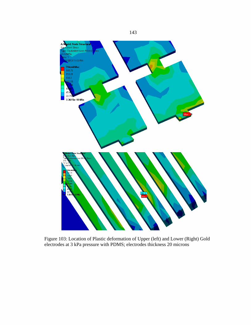
143
Figure 103: Location of Plastic deformation of Upper (left) and Lower (Right) Gold
electrodes at 3 kPa pressure with PDMS; electrodes thickness 20 microns

144
Figure 104: Location of the beginning of Plastic deformation of Bumps at 7 kPa pressure
with PDMS and Gold; electrodes thickness 20 microns
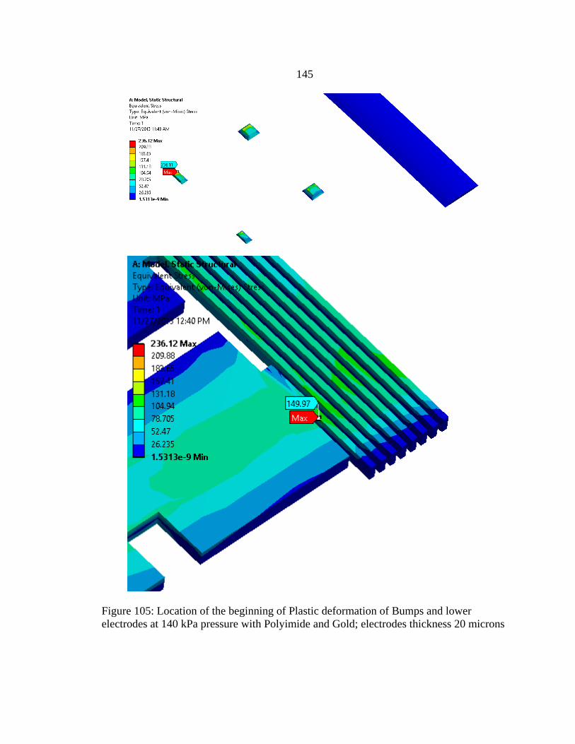
145
Figure 105: Location of the beginning of Plastic deformation of Bumps and lower
electrodes at 140 kPa pressure with Polyimide and Gold; electrodes thickness 20 microns

146
Figure 106: Location of the beginning of Plastic deformation of upper electrodes at 170
kPa pressure with Polyimide and Gold; electrodes thickness 20 microns
Figure 107: Max Equivalent Thermal Stress; Material:PDMS and Gold

147
Figure 108: Maximum Equivalent Thermal and Mechanical Strain; Material: PDMS and
Gold
Figure 109: Max Equivalent Thermal Stress; Material: PDMS and Copper

148
Figure 110: Maximum Equivalent Thermal and Mechanical Strain; Material: PDMS and
Copper
Figure 111: Max Equivalent Thermal Stress ; Material: Polyimide and Gold

149
Figure 112: Maximum Equivalent Thermal and Mechanical Strain; Material: Polyimide
and Gold
Figure 113: Max Equivalent Thermal Stress; Material: Polyimide and Copper

150
Figure 114: Maximum Equivalent Thermal and Mechanical Strain; Material: Polyimide
and Copper

151
APPENDIX B:
ANSYS MECHANICAL APDL CODE

152
finish
/clear
/prep7
ET,1,182,,,0 ! Element Type 1 is 182 ;keyopt(3)=0 is defined as 'plane stress'
condition
MP,ex,1,7e-1 !defining PDMS properties
MP,NUXY,1,0.49999
MP,ALPX,1,310E-6 ! Coefficient of thermal extension for PDMS, 310
!MICRO_STRAIN/kELVIN
MP,ex,2,2500 !defining Polyimide properties
MP,NUXY,2,0.34
MP,ALPX,2,20E-6 ! Coefficient of thermal extension for Polyimide,20
!MICRO_STRAIN/kELVIN
MP,ex,3,7.9e4 !defining Gold Properties
MP,NUXY,3,0.42
MP,ALPX,3,14.2E-6 !Coefficient of thermal extension for Gold, 14.2
!MICRO_STRAIN/KELVIN
!!MP,ex,3,1.1e5 !defining Copper Properties
!!MP,NUXY,3,0.34
!!MP,ALPX,3,17E-6 !Coefficient of thermal extension for
!Copper, 17 MICRO_STRAIN/KELVIN
!!Tensile Yield strength of PDMS is 2.24 MPa
!!gold yield strength is 127 Mpa
!!Copper yield strength is 252.3Mpa
!!Polyimide yield strength is 231Mpa (tensile) and 150 Mpa (compressive)
!!Creating Geometry
lepdms=0.292 !length of pdms substrate 500 micron
leelec=0.2 ! length of electrodes are 200 micron
welec=0.02 ! width of electrodes 20 micron initial
bumpl=.042 ! Bump Length is 42 micron
bumpw= 0.01 ! Bump height 10 micron
wpdms=0.1 ! width of upper and lower pdms is 100
micron
!!wgap=0.01 ! air gap width 10 micron
!!wpoly=0.01 ! pdms spacer thickness 10 micron
blc4,0,0,lepdms,wpdms ! lowerpdms
blc4,0,wpdms,bumpl,bumpw ! left pillar
blc4,.046,wpdms-welec,0.2,welec ! lower electrodes
blc4,0.25,wpdms,bumpl,bumpw ! right pillar
!!!!!!!!blc4,0,wpdms,lepdms,wgap ! air gap

153
!!! Temporarily deactivating blc4,0,wpdms+wgap,lepdms,wpoly !! Polyimide
!!!solid layer
blc4,0.046,wpdms+bumpw,0.2,welec ! Upper electrodes
blc4,0,wpdms+bumpw,lepdms,wpdms ! Upper pdms
blc4,0.042,wpdms,0.208,bumpw ! Middle air gap
!!a,21,8,5,4
!!a,22,3,14,15
!!a,7,16,13,6
allsel,all
aovlap,all
aglue,all
aplot
allsel,all
sys_num=11
local,sys_num,0,0.042,,,,,90 !arbitrary reference number greater than
!10 that’s why sys_num=11
wpcsys,-1,sys_num
asbw,all,,delete
sys_num=sys_num+1 !increment numbering by 1 each time
local,sys_num,0,.046,,,,,90 !create new coordinate system (translated and rotated)
wpcsys,-1,sys_num !define working plane at that new coordinate system
asbw,all,,delete !divide areas along working plane (basically cutting
geometry at !intersection with plane)
sys_num=sys_num+1
local,sys_num,0,.246,,,,,90
wpcsys,-1,sys_num
asbw,all,,delete
sys_num=sys_num+1
local,sys_num,0,.35,,,,,90
wpcsys,-1,sys_num
asbw,all,,delete
sys_num=sys_num+1
local,sys_num,0,0.25,,,,,90
wpcsys,-1,sys_num
asbw,all,,delete
sys_num=sys_num+1
local,sys_num,0,,wpdms-welec,,,90,
wpcsys,-1,sys_num
asbw,all,,delete
sys_num=sys_num+1

154
local,sys_num,0,,wpdms+bumpw+welec,,,90,
wpcsys,-1,sys_num
asbw,all,,delete
csys,0
wpcsys,-1,0
!!!!!!!!!!!!!!!!!!!!!!!!!!!!!!!!!!!!!!!!!!!!!!!!!!!!!!!
!!!!!!!!!!!!!!!!!!!!!!!!!!!!!!!!!!!!!!!!!!!!!!!!!!!!!!!
/pnum,line,0
/pnum,area,1
type,1
mshkey,1 !!mapped meshing is turned on
mshape,0 !Specifying element shape, triangular element
asel,s,area,,5
asel,a,area,,3
cm,electrodes,area ! Groups Geometry Items into components
asel,s,area,,8
asel,a,area,,9
cm,bump,area
asel,s,area,,7
asel,a,area,,4
asel,a,area,,10
cm,airgap,area
allsel,all
asel,u,area,,airgap !unselecting airgap and electrodes from all areas
asel,u,area,,electrodes
esize,0.003
mat,2 ! Meshing with material type 2 (Polyimide) and 1
!(PDMS) alternatively
amesh,all ! Meshed all areas except airgap and electrodes
!with Element size 0.003mm or 3 micron
mshkey,1 ! Mapped meshing turned on
mshape,0 !use quad elements
esize,0.002
asel,s,area,,electrodes
mat,3 ! Selected electrode material is Gold or copper
amesh,all
allsel,all
nsel,s,loc,y,0
d,all,ux,0 ! Defining Boundary Conditions at the base
d,all,uy,0
!!allsel,all

155
!!nsel,s,loc,x,0
!!nsel,a,loc,x,lepdms
!!d,all,ux,0
!!et,2,targe169 ! Element type 2 is a target element 169
!!et,3,conta171 ! Element type 3 is a contact element 171
!!keyopt,3,12,0
!!allsel,all
!!lsel,s,loc,x,0.042,0.25
!!lsel,r,loc,y,wpdms
!!nsll,r,1
!!type,2
!!esurf,, !Generates elements overlaid on the free faces of
existing !selected elements
!!allsel,all
!!lsel,s,loc,x,0.042,0.25
!!lsel,r,loc,y,wpdms+bumpw
!!nsll,r,1 !Selects those nodes associated with the selected
!lines
!!type,3
!!esurf,,
finish
/SOLU
nlgeom,on
antype,static
outres,all
!nropt,full,,off
!neqit,100
nsel,all
allsel,all
TREF,100 !Defines the reference temperature of thermal strain
!calculation
TUNIF,22 !Assigns a uniform temperature to all nodes
allsel,all
solve
FINISH
/post1