
Design and Characterization of Submicron CCDs in CMOS Workshops/2009 Workshop/2009 Papers/048... ·...
4
Design and Characterization of Submicron CCDs in CMOS Keith Fife, Abbas El Gamal and H.-S. Philip Wong Department of Electrical Engineering, Stanford University, Stanford, CA 94305 Phone: 650-725-9696, Fax: 650-724-3648, E-mail: [email protected] Abstract Three types of submicron CCDs are implemented in single- poly 0.11μm CMOS technology to demonstrate the feasibility of multi-aperture imaging systems that produce data from distributed arrays of CCDs integrated across a monolithic substrate. Test structures comprising 16 × 16 pixel Frame- Transfer (FT)-CCDs with 0.5 - 0.7μm pixels are fabricated under various process conditions to implement devices which operate as surface-channel, buried-channel and pinned phase buried-channel. Ripple charge transfer and single electrode charge confinement are implemented to minimize pixel pitch. Introduction As pixel size is approaching the limits of conventional optics, improvements in resolution are diminishing. Scaling pixels beyond these limits, however, can provide new imaging capabilities beyond merely attempting to increase spatial resolution. In [1], we describe a multi-aperture approach to imaging, whereby the image sensor is partitioned into an array of apertures, each with its own local subarray of pixels and image-forming optics. A real image is focused a certain distance above the sensor such that the apertures capture overlapping views of the scene. The subimages are post- processed to obtain both a high resolution 2D image and a depth map. A key feature of this design is in the use of submicron pixels to obtain accurate depth measurements derived from the localization of features within adjacent subarrays. Other benefits of this configuration include the ability to image objects at close proximity to the sensor without the need for objective optics, achieve nearly complete color separation through a per-aperture color filter array, relax the requirements on the camera objective optics, and increase the tolerance to defective pixels. The architecture is also highly scalable, making it possible to increase pixel counts well beyond current levels. Building submicron CMOS pixels with acceptable imaging performance at wide apertures is challenging because of the high dielectric stack height and optical occlusions resulting from the use of metal layers in the pixel. It has recently become possible to implement deeply scaled CCD pixels in modern CMOS due to the narrow poly gap spacing. This eliminates the need for processing multi-layer polysilicon and allows for electrode widths roughly equal to the gap spacing, which increases the effective quantum efficiency. Since the poly gap region normally creates either a pocket or a barrier, we make use of this feature to achieve single electrode charge confinement. The need for anti-blooming and high charge transfer efficiency are relaxed by the multi-aperture architecture where smaller subarrays are distributed globally. This paper presents the design and characterization of 3 types of CCD structures implemented in 0.11μm CMOS tech- nology: surface-channel, buried-channel, and pinned phase buried-channel. Each CCD structure differs in the location of charge storage during the integration time and in the sequencing of the electrodes during charge transfer. Our surface-channel design at 0.5μm pixel pitch was first reported in [2]. We used the buried-channel CCD design in a multi- aperture image sensor reported in [3]. A new pinned phase buried-channel design is implemented to improve both dark current and charge transfer efficiency. We use the poly gap region as an area for self-aligned implantation to create barriers that allow for inversion of the channel during the integration period. To characterize our designs, we fabricated test structures comprising arrays of 16 × 16, pixel FT-CCDs, each with source follower readout. We first discuss the design, fabrication, and operation of the image sensor, and then present simulation and characterization results. Design, Fabrication, and Operation We use an FT-CCD architecture to minimize pixel pitch and to eliminate metal layers in the active imaging area. We make the format of each sensor approximately equal to the dielectric stack height, which enables f/1 scale apertures for high sensitivity. We take advantage of the fact that the image capture is a distributed process by partitioning the subarrays into regions of high fill factor and occlusion free optical paths. Implementing the CCDs in CMOS enables fast multi- array readout along with the integration of analog and digital circuits. Each test structure consists of a pixel array, a storage array, a horizontal (H)-CCD, and a source follower readout circuit (see Fig. 1). The storage array is covered by metal layers that are also used to distribute global control lines (see Fig. 2). A photomicrograph is shown in Fig. 3. Each pixel consists of a single poly electrode, a channel, and a channel stop. The channels and stops for the surface-channel devices are shown in Fig. 4. The electrodes are patterned with non- silicided polysilicon as shown in Fig. 5. Each pixel array is separated by a wall of 4 metal layers. The first 2 metal layers are shown in Fig. 6. In all designs, the polysilicon is doped by masking out the channels as shown in Fig. 7. The resolution of the S/D implant masks were the limiting factor in scaling beyond 0.5μm pixel pitch at this process node. We expect that it is possible to pre-dope the polysilicon before etch to scale the pixel size further. The polysilicon for the surface-channel device is doped N+ and the buried-channel designs are doped P+ to shift the workfunction closer to the operating range of CMOS circuits. The IOs on the test chip were designed to allow both positive and negative voltage sequencing. SEM images for each cross section of the surface-channel device are shown in Fig. 8 and Fig. 9. An electrode spacing of 180nm was used in all designs. The polysilicon is 130nm thick with gate oxide of 8nm. The channel stop for the surface-channel device is Shallow Trench Isolation (STI). The channel stop for the buried-channel is formed by a P-type implant (BF2, 75keV, 4.0E13/cm 2 ). The SEM for the H-CCD with fill-and-
Transcript of Design and Characterization of Submicron CCDs in CMOS Workshops/2009 Workshop/2009 Papers/048... ·...

Design and Characterization of Submicron CCDs in CMOSKeith Fife, Abbas El Gamal and H.-S. Philip Wong
Department of Electrical Engineering, Stanford University, Stanford, CA 94305Phone: 650-725-9696, Fax: 650-724-3648, E-mail: [email protected]
AbstractThree types of submicron CCDs are implemented in single-poly 0.11µm CMOS technology to demonstrate the feasibilityof multi-aperture imaging systems that produce data fromdistributed arrays of CCDs integrated across a monolithicsubstrate. Test structures comprising16 × 16 pixel Frame-Transfer (FT)-CCDs with0.5 − 0.7µm pixels are fabricatedunder various process conditions to implement devices whichoperate as surface-channel, buried-channel and pinned phaseburied-channel. Ripple charge transfer and single electrodecharge confinement are implemented to minimize pixel pitch.
IntroductionAs pixel size is approaching the limits of conventional optics,improvements in resolution are diminishing. Scaling pixelsbeyond these limits, however, can provide new imagingcapabilities beyond merely attempting to increase spatialresolution. In [1], we describe a multi-aperture approach toimaging, whereby the image sensor is partitioned into anarray of apertures, each with its own local subarray of pixelsand image-forming optics. A real image is focused a certaindistance above the sensor such that the apertures captureoverlapping views of the scene. The subimages are post-processed to obtain both a high resolution 2D image anda depth map. A key feature of this design is in the useof submicron pixels to obtain accurate depth measurementsderived from the localization of features within adjacentsubarrays. Other benefits of this configuration include theability to image objects at close proximity to the sensorwithout the need for objective optics, achieve nearly completecolor separation through a per-aperture color filter array,relaxthe requirements on the camera objective optics, and increasethe tolerance to defective pixels. The architecture is alsohighly scalable, making it possible to increase pixel countswell beyond current levels.
Building submicron CMOS pixels with acceptable imagingperformance at wide apertures is challenging because of thehigh dielectric stack height and optical occlusions resultingfrom the use of metal layers in the pixel. It has recentlybecome possible to implement deeply scaled CCD pixels inmodern CMOS due to the narrow poly gap spacing. Thiseliminates the need for processing multi-layer polysiliconand allows for electrode widths roughly equal to the gapspacing, which increases the effective quantum efficiency.Since the poly gap region normally creates either a pocket orabarrier, we make use of this feature to achieve single electrodecharge confinement. The need for anti-blooming and highcharge transfer efficiency are relaxed by the multi-aperturearchitecture where smaller subarrays are distributed globally.
This paper presents the design and characterization of 3types of CCD structures implemented in 0.11µm CMOS tech-nology: surface-channel, buried-channel, and pinned phaseburied-channel. Each CCD structure differs in the location
of charge storage during the integration time and in thesequencing of the electrodes during charge transfer. Oursurface-channel design at 0.5µm pixel pitch was first reportedin [2]. We used the buried-channel CCD design in a multi-aperture image sensor reported in [3]. A new pinned phaseburied-channel design is implemented to improve both darkcurrent and charge transfer efficiency. We use the poly gapregion as an area for self-aligned implantation to createbarriers that allow for inversion of the channel during theintegration period. To characterize our designs, we fabricatedtest structures comprising arrays of16 × 16, pixel FT-CCDs,each with source follower readout. We first discuss the design,fabrication, and operation of the image sensor, and thenpresent simulation and characterization results.
Design, Fabrication, and Operation
We use an FT-CCD architecture to minimize pixel pitch andto eliminate metal layers in the active imaging area. Wemake the format of each sensor approximately equal to thedielectric stack height, which enables f/1 scale aperturesforhigh sensitivity. We take advantage of the fact that the imagecapture is a distributed process by partitioning the subarraysinto regions of high fill factor and occlusion free opticalpaths. Implementing the CCDs in CMOS enables fast multi-array readout along with the integration of analog and digitalcircuits. Each test structure consists of a pixel array, a storagearray, a horizontal (H)-CCD, and a source follower readoutcircuit (see Fig. 1). The storage array is covered by metallayers that are also used to distribute global control lines(seeFig. 2). A photomicrograph is shown in Fig. 3. Each pixelconsists of a single poly electrode, a channel, and a channelstop. The channels and stops for the surface-channel devicesare shown in Fig. 4. The electrodes are patterned with non-silicided polysilicon as shown in Fig. 5. Each pixel array isseparated by a wall of 4 metal layers. The first 2 metal layersare shown in Fig. 6.
In all designs, the polysilicon is doped by masking outthe channels as shown in Fig. 7. The resolution of the S/Dimplant masks were the limiting factor in scaling beyond0.5µm pixel pitch at this process node. We expect that itis possible to pre-dope the polysilicon before etch to scalethe pixel size further. The polysilicon for the surface-channeldevice is doped N+ and the buried-channel designs are dopedP+ to shift the workfunction closer to the operating rangeof CMOS circuits. The IOs on the test chip were designedto allow both positive and negative voltage sequencing. SEMimages for each cross section of the surface-channel deviceare shown in Fig. 8 and Fig. 9. An electrode spacing of 180nmwas used in all designs. The polysilicon is 130nm thick withgate oxide of 8nm. The channel stop for the surface-channeldevice is Shallow Trench Isolation (STI). The channel stopfor the buried-channel is formed by a P-type implant (BF2,75keV, 4.0E13/cm2). The SEM for the H-CCD with fill-and-
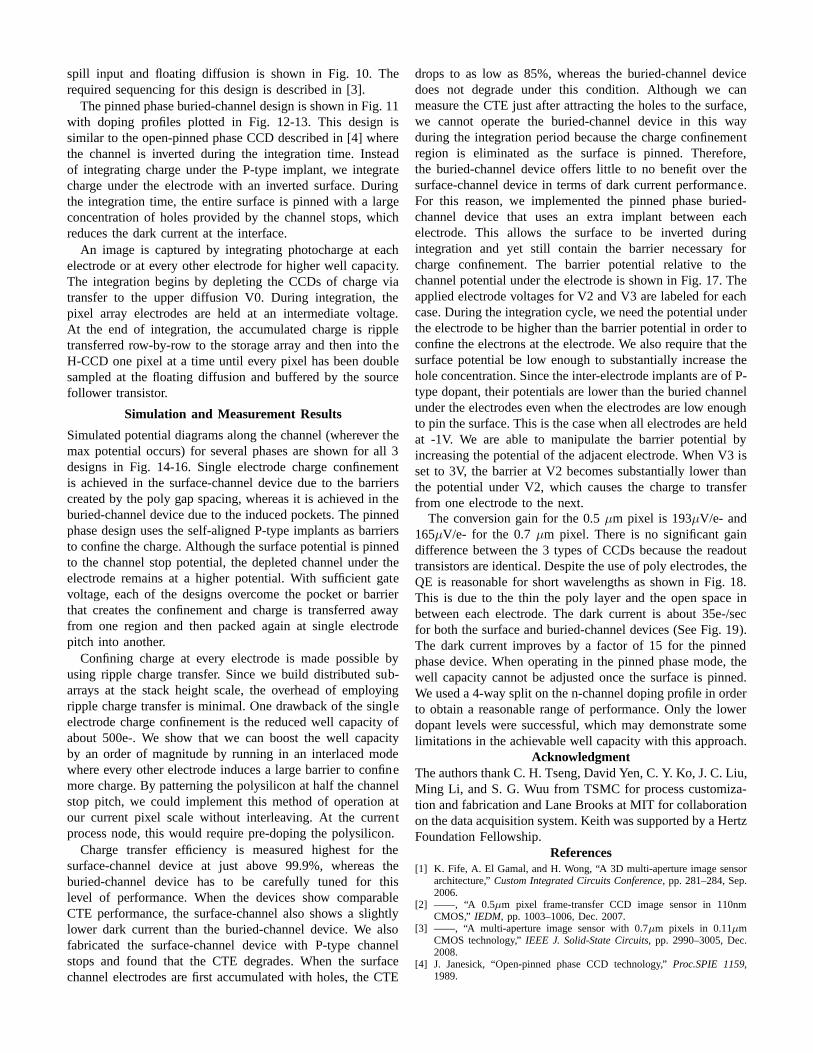
spill input and floating diffusion is shown in Fig. 10. Therequired sequencing for this design is described in [3].
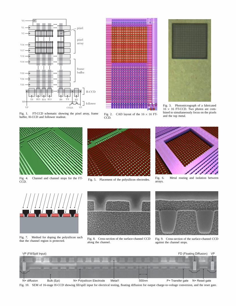
The pinned phase buried-channel design is shown in Fig. 11with doping profiles plotted in Fig. 12-13. This design issimilar to the open-pinned phase CCD described in [4] wherethe channel is inverted during the integration time. Insteadof integrating charge under the P-type implant, we integratecharge under the electrode with an inverted surface. Duringthe integration time, the entire surface is pinned with a largeconcentration of holes provided by the channel stops, whichreduces the dark current at the interface.
An image is captured by integrating photocharge at eachelectrode or at every other electrode for higher well capacity.The integration begins by depleting the CCDs of charge viatransfer to the upper diffusion V0. During integration, thepixel array electrodes are held at an intermediate voltage.At the end of integration, the accumulated charge is rippletransferred row-by-row to the storage array and then into theH-CCD one pixel at a time until every pixel has been doublesampled at the floating diffusion and buffered by the sourcefollower transistor.
Simulation and Measurement Results
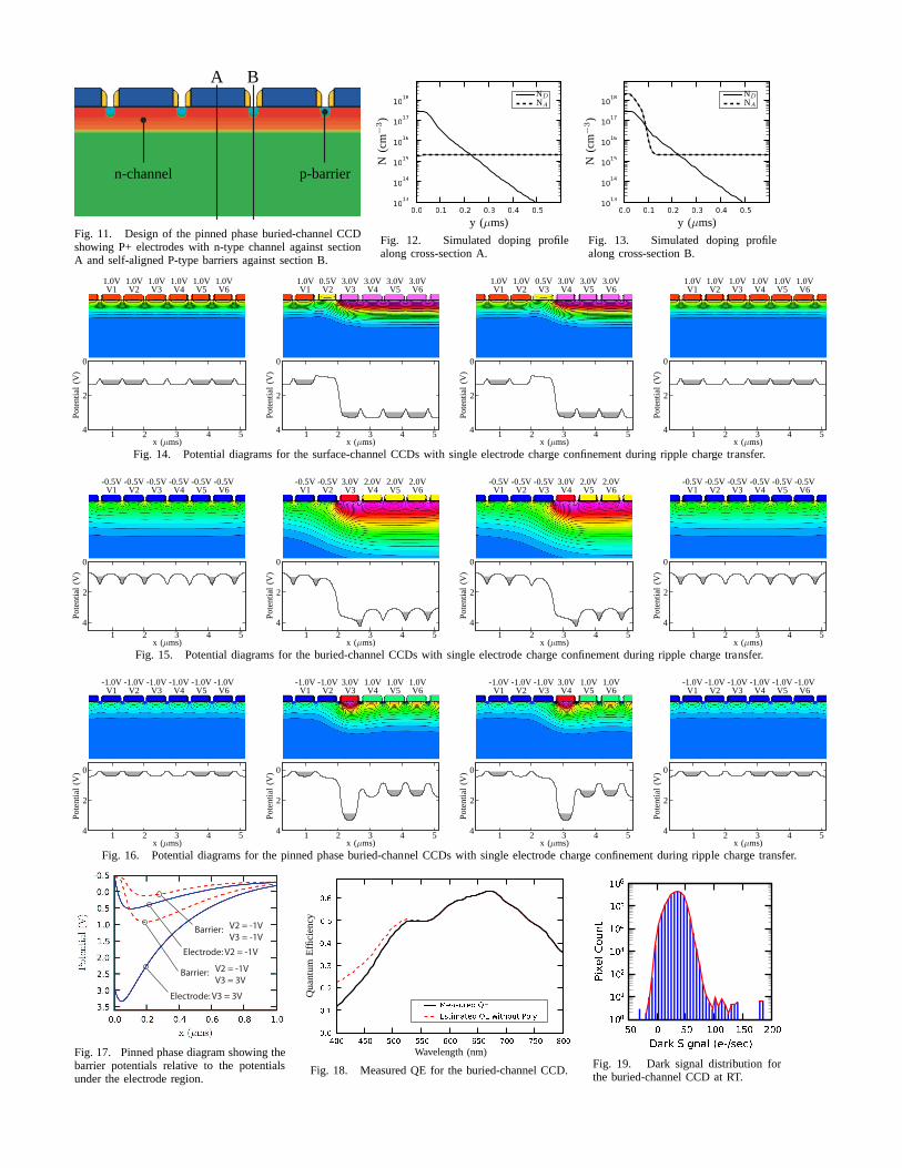
Simulated potential diagrams along the channel (wherever themax potential occurs) for several phases are shown for all 3designs in Fig. 14-16. Single electrode charge confinementis achieved in the surface-channel device due to the barrierscreated by the poly gap spacing, whereas it is achieved in theburied-channel device due to the induced pockets. The pinnedphase design uses the self-aligned P-type implants as barriersto confine the charge. Although the surface potential is pinnedto the channel stop potential, the depleted channel under theelectrode remains at a higher potential. With sufficient gatevoltage, each of the designs overcome the pocket or barrierthat creates the confinement and charge is transferred awayfrom one region and then packed again at single electrodepitch into another.
Confining charge at every electrode is made possible byusing ripple charge transfer. Since we build distributed sub-arrays at the stack height scale, the overhead of employingripple charge transfer is minimal. One drawback of the singleelectrode charge confinement is the reduced well capacity ofabout 500e-. We show that we can boost the well capacityby an order of magnitude by running in an interlaced modewhere every other electrode induces a large barrier to confinemore charge. By patterning the polysilicon at half the channelstop pitch, we could implement this method of operation atour current pixel scale without interleaving. At the currentprocess node, this would require pre-doping the polysilicon.
Charge transfer efficiency is measured highest for thesurface-channel device at just above 99.9%, whereas theburied-channel device has to be carefully tuned for thislevel of performance. When the devices show comparableCTE performance, the surface-channel also shows a slightlylower dark current than the buried-channel device. We alsofabricated the surface-channel device with P-type channelstops and found that the CTE degrades. When the surfacechannel electrodes are first accumulated with holes, the CTE
drops to as low as 85%, whereas the buried-channel devicedoes not degrade under this condition. Although we canmeasure the CTE just after attracting the holes to the surface,we cannot operate the buried-channel device in this wayduring the integration period because the charge confinementregion is eliminated as the surface is pinned. Therefore,the buried-channel device offers little to no benefit over thesurface-channel device in terms of dark current performance.For this reason, we implemented the pinned phase buried-channel device that uses an extra implant between eachelectrode. This allows the surface to be inverted duringintegration and yet still contain the barrier necessary forcharge confinement. The barrier potential relative to thechannel potential under the electrode is shown in Fig. 17. Theapplied electrode voltages for V2 and V3 are labeled for eachcase. During the integration cycle, we need the potential underthe electrode to be higher than the barrier potential in order toconfine the electrons at the electrode. We also require that thesurface potential be low enough to substantially increase thehole concentration. Since the inter-electrode implants are of P-type dopant, their potentials are lower than the buried channelunder the electrodes even when the electrodes are low enoughto pin the surface. This is the case when all electrodes are heldat -1V. We are able to manipulate the barrier potential byincreasing the potential of the adjacent electrode. When V3 isset to 3V, the barrier at V2 becomes substantially lower thanthe potential under V2, which causes the charge to transferfrom one electrode to the next.
The conversion gain for the 0.5µm pixel is 193µV/e- and165µV/e- for the 0.7µm pixel. There is no significant gaindifference between the 3 types of CCDs because the readouttransistors are identical. Despite the use of poly electrodes, theQE is reasonable for short wavelengths as shown in Fig. 18.This is due to the thin the poly layer and the open space inbetween each electrode. The dark current is about 35e-/secfor both the surface and buried-channel devices (See Fig. 19).The dark current improves by a factor of 15 for the pinnedphase device. When operating in the pinned phase mode, thewell capacity cannot be adjusted once the surface is pinned.We used a 4-way split on the n-channel doping profile in orderto obtain a reasonable range of performance. Only the lowerdopant levels were successful, which may demonstrate somelimitations in the achievable well capacity with this approach.
AcknowledgmentThe authors thank C. H. Tseng, David Yen, C. Y. Ko, J. C. Liu,Ming Li, and S. G. Wuu from TSMC for process customiza-tion and fabrication and Lane Brooks at MIT for collaborationon the data acquisition system. Keith was supported by a HertzFoundation Fellowship.
References[1] K. Fife, A. El Gamal, and H. Wong, “A 3D multi-aperture image sensor
architecture,”Custom Integrated Circuits Conference, pp. 281–284, Sep.2006.
[2] ——, “A 0.5µm pixel frame-transfer CCD image sensor in 110nmCMOS,” IEDM, pp. 1003–1006, Dec. 2007.
[3] ——, “A multi-aperture image sensor with 0.7µm pixels in 0.11µmCMOS technology,”IEEE J. Solid-State Circuits, pp. 2990–3005, Dec.2008.
[4] J. Janesick, “Open-pinned phase CCD technology,”Proc.SPIE 1159,1989.
pixel
pixel
array
frame
buffer
follower
H-CCD
V0
V1
V2
V16
V17
V18
V19
V33
V34
V35
TS H15 H14 H13 H0 TX RTRS
VPVP COLB
Fig. 1. FT-CCD schematic showing the pixel array, framebuffer, H-CCD and follower readout.
Fig. 2. CAD layout of the16 × 16 FT-CCD.
Fig. 3. Photomicrograph of a fabricated16 × 16 FT-CCD. Two photos are com-bined to simultaneously focus on the pixelsand the top metal.
Fig. 4. Channel and channel stops for the FT-CCD.
Fig. 5. Placement of the polysilicon electrodes.Fig. 6. Metal routing and isolation betweenarrays.
Fig. 7. Method for doping the polysilicon suchthat the channel region is protected.
Fig. 8. Cross-section of the surface-channel CCDalong the channel.
Fig. 9. Cross-section of the surface-channel CCDagainst the channel stops.
VP (Fill/Spill Input) FD (Floating Diffusion) VP
N+ diffusion Bulk (Epi) N+ Polysilicon Electrode P+ Transfer gate N+ Reset gateMetal1 500nm
Fig. 10. SEM of 16-stage H-CCD showing fill/spill input for electrical testing, floating diffusion for output charge-to-voltage conversion, and the reset gate.
n-channel p-barrier
A B
Fig. 11. Design of the pinned phase buried-channel CCDshowing P+ electrodes with n-type channel against sectionA and self-aligned P-type barriers against section B.
0.0 0.1 0.2 0.3 0.4 0.510
13
1014
1015
1016
1017
1018
N(c
m−
3)
y (µms)
ND
NA
Fig. 12. Simulated doping profilealong cross-section A.
0.0 0.1 0.2 0.3 0.4 0.510
13
1014
1015
1016
1017
1018
N(c
m−
3)
y (µms)
ND
NA
Fig. 13. Simulated doping profilealong cross-section B.
Pot
entia
l(V
)
x (µms)
V1 V2 V3 V4 V5 V61.0V1.0V1.0V1.0V1.0V1.0V
0
1
2
2 34 4 5
Pot
entia
l(V
)
x (µms)
V1 V2 V3 V4 V5 V60.5V1.0V 3.0V3.0V3.0V3.0V
0
1
2
2 34 4 5
Pot
entia
l(V
)
x (µms)
V1 V2 V3 V4 V5 V60.5V1.0V1.0V 3.0V3.0V3.0V
0
1
2
2 34 4 5
Pot
entia
l(V
)
x (µms)
V1 V2 V3 V4 V5 V61.0V1.0V1.0V1.0V1.0V1.0V
0
1
2
2 34 4 5
Fig. 14. Potential diagrams for the surface-channel CCDs with single electrode charge confinement during ripple charge transfer.
Pot
entia
l(V
)
x (µms)
V1 V2 V3 V4 V5 V6-0.5V-0.5V-0.5V-0.5V-0.5V-0.5V
0
1
2
2 34
4 5
Pot
entia
l(V
)
x (µms)
V1 V2 V3 V4 V5 V6-0.5V-0.5V 2.0V2.0V2.0V3.0V
0
1
2
2 34
4 5
Pot
entia
l(V
)
x (µms)
V1 V2 V3 V4 V5 V6-0.5V-0.5V-0.5V 2.0V2.0V3.0V
0
1
2
2 34
4 5
Pot
entia
l(V
)
x (µms)
V1 V2 V3 V4 V5 V6-0.5V-0.5V-0.5V-0.5V-0.5V-0.5V
0
1
2
2 34
4 5
Fig. 15. Potential diagrams for the buried-channel CCDs withsingle electrode charge confinement during ripple charge transfer.
Pot
entia
l(V
)
x (µms)
V1 V2 V3 V4 V5 V6-1.0V-1.0V-1.0V-1.0V-1.0V-1.0V
0
1
2
2 34 4 5
Pot
entia
l(V
)
x (µms)
V1 V2 V3 V4 V5 V6-1.0V-1.0V 1.0V1.0V1.0V3.0V
0
1
2
2 34 4 5
Pot
entia
l(V
)
x (µms)
V1 V2 V3 V4 V5 V6-1.0V-1.0V-1.0V 1.0V1.0V3.0V
0
1
2
2 34 4 5
Pot
entia
l(V
)
x (µms)
V1 V2 V3 V4 V5 V6-1.0V-1.0V-1.0V-1.0V-1.0V-1.0V
0
1
2
2 34 4 5
Fig. 16. Potential diagrams for the pinned phase buried-channel CCDs with single electrode charge confinement during ripple charge transfer.
Electrode: V3 = 3V
Electrode: V2 = -1V
V2 = -1V
V3 = 3VBarrier:
V2 = -1V
V3 = -1VBarrier:
Fig. 17. Pinned phase diagram showing thebarrier potentials relative to the potentialsunder the electrode region.
4 0 0 4 5 0 5 0 0 5 5 0 6 0 0 6 5 0 7 0 0 7 5 0 8 0 00 . 00 . 10 . 20 . 30 . 40 . 50 . 6M e a s u r e d Q EE s t i m a t e d Q E w i t h o u t P o l yQ
uant
umE
ffici
ency
Wavelength (nm)
Fig. 18. Measured QE for the buried-channel CCD.
� 5 0 0 5 0 1 0 0 1 5 0 2 0 0D a r k S i g n a l ( e , / s e c )1 0 01 0 11 0 21 0 31 0 41 0 51 0 6Pi xelC ountFig. 19. Dark signal distribution forthe buried-channel CCD at RT.