DESIGN AND CHARACTERIZATION OF OSCILLATOR TOPOLOGIES ...
68
i DESIGN AND CHARACTERIZATION OF OSCILLATOR TOPOLOGIES. COMPARATIVE WITH OTHER TOPOLOGIES Verónica Do Amaral Rosal Master’s Thesis presented to the Telecommunications Engineering School Master’s Degree in Telecommunications Engineering Supervisors Ana María Cao Paz María Loreto Rodríguez Pardo 2020
Transcript of DESIGN AND CHARACTERIZATION OF OSCILLATOR TOPOLOGIES ...

i
DESIGN AND CHARACTERIZATION OF OSCILLATOR
TOPOLOGIES. COMPARATIVE WITH OTHER TOPOLOGIES
Verónica Do Amaral Rosal
Master’s Thesis presented to the Telecommunications Engineering School
Master’s Degree in Telecommunications Engineering
Supervisors Ana María Cao Paz
María Loreto Rodríguez Pardo
2020

ii

iii
Abstract
This work consists of the design and characterization of two oscillating topologies at 9MHz for
use as quartz microbalance sensors. These topologies are the Clapp and the Colpitts, belonging
to the Pierce family.
Initially, the oscillator circuits corresponding to each topology are designed. For their
characterization as quartz microbalance sensors, both topologies are performed behavioural
tests under mass deposition on their surface and in liquid media with different densities and
viscosities.
Subsequently, the study of two other designs already created with ABO and Miller topologies is
carried out and their behaviours as quartz microbalance sensors is characterized.
Finally, a comparison is made between the four different topologies.
Keywords
Crystal oscillators, Frequency, Load contributions, Quartz Crystal Microbalance (QCM) sensor,
Piezoelectricity, Resonators.

iv
Contents Abstract ........................................................................................................................................ iii
List of abbreviations and symbols ................................................................................................. v
1. Introduction .......................................................................................................................... 1
2. Quartz crystal microbalance sensors .................................................................................... 3
2.1. Quartz crystal ................................................................................................................ 3
2.2. Quartz crystal resonator as QCM sensor ...................................................................... 9
2.2.1. Coated quartz crystal .......................................................................................... 10
2.2.2. Load contributions .............................................................................................. 13
3. Oscillator circuits for QCM sensors ..................................................................................... 16
3.1. Sinusoidal oscillators ................................................................................................... 16
3.1.1. RC Oscillators ....................................................................................................... 17
3.1.2. LC oscillators ........................................................................................................ 19
3.2. Crystal oscillators ........................................................................................................ 20
3.2.1. Pierce family ........................................................................................................ 22
4. Design and characterization of Clapp and Colpitts oscillating topologies .......................... 28
4.1. 9 MHz Clapp oscillator ................................................................................................. 28
4.1.1. 9 MHz Clapp oscillator circuit .............................................................................. 28
4.1.2. Oscillation frequency adjustment ....................................................................... 29
4.1.3. Characterization with mass charge and in liquid medium .................................. 31
4.1.4. Circuit test and board design .............................................................................. 35
4.2. 9 MHz Colpitts oscillator ............................................................................................. 37
4.2.1. 9 MHz Colpitts oscillator circuit .......................................................................... 37
4.2.2. Frequency adjustment ........................................................................................ 38
4.2.3. Characterization with mass charge and in liquid medium .................................. 40
4.2.4. Board design ........................................................................................................ 43
5. Comparative of the designed topologies with others already implemented ..................... 43
5.1. Characterization of the topologies already implemented .......................................... 43
5.1.1. 9 MHz ABO oscillator ........................................................................................... 43
5.1.2. 9 MHz Miller oscillator ........................................................................................ 49
5.2. Analysis of the obtained results .................................................................................. 56
6. Results, conclusions and future lines .................................................................................. 58
7. Bibliographic references ..................................................................................................... 59

v
List of abbreviations and symbols
Abbreviations used in the text:
ABO Active Bridge Oscillator AGC Automatic Gain Control BVD Butterworth Van-Dyke FET Field Effect Transistor FFT Fast Fourier Transform PCB Printed Circuit Board QCM Quartz Cristal Microbalance SBO Standard Bridge Oscillator SHBO Standard Half-Bridge Oscillator TLM Transmission Line Mode
Symbols used in equations and in text:
N AT constant. d Quartz disc thickness. ε22 Quartz permittivity. ηq Quartz effective viscosity. 𝐶66 Shear modulus. cq Complex shear modulus. e26 Piezoelectric stress constant. ρq Quartz density. As Effective area of electrode surface. hq Quartz thickness constant. Cp Static capacity. Rq Dynamic resistance of the crystal without load. Lq Dynamic inductance of the crystal without load. Cq Dynamic capacitance of the crystal without load. K0 Lossless effective electromechanical coupling factor. Kq Lossy effective electromechanical coupling factor. n Harmonic resonance of quartz. ωs Angular frequency. fs Serial frequency. fr Parallel frequency. Q Quartz crystal quality factor fo Oscillation frequency. Z Electrical complex impedance of the sensor. αq Complex phase of acoustic wave through lossy quartz. ZL Superficial load impedance. Zq Characteristic impedance of quartz. Zm Dynamic impedance associated with the electro-mechanical vibration of the sensor. Zm
q Dynamic impedance of the quartz without load. Zm
m Total load contribution to sensor dynamic impedance. Rm Load contribution to dynamic resistance. Cm Load contribution to dynamic capacitance. Lm Total load contribution to dynamic impedance. Lm1 Load contribution to dynamic impedance for liquid load Lm2 Load contribution to dynamic impedance for mass load

vi
Y Admitance. C0 Quartz crystal external capacity. C0* Sum of C0 and Cp. Gs Sensor conductance. B Sensor susceptance. ηL Absolute viscosity of the liquid. ρL Liquid density. kl Kanawaza sensibility factor. ks Sauerbrey sensibility factor. H(jωo) Open loop transfer function. G Total oscillator gain. A Voltage gain. β Feedback gain.

vii
1
1. Introduction
Crystal oscillators were invented in the 1920s. Cady made one of the first ones in 1921. Miller
patented both his own and Pierce’s circuits in 1930. Pierce patented both his own and Miller’s
circuits in 1931, and after some legal arguing in the courts, Pierce repatented both circuits again
in 1938. Sabaroff’s quartz crystal version of the Colpitts LC oscillator was published in 1937, and
Meacham’s resistance bridge circuit was published in 1938. Butler published his article on VHF
harmonic oscillators in 1946. Goldberg and Crosby published their article on cathode coupled or
grounded grid oscillators in 1948.
The U.S. Army Signal Corps funded an intense quartz crystal development program during and
after World War II and funded a small amount of oscillator circuit development along the way.
Edson conducted a study of VHF harmonic oscillator circuits in 1950 and published his classic
book on vacuum tube oscillators of all types in 1953. In 1965, Firth published his design
handbook of the Pierce circuit and the Butler common base harmonic circuit [Matthys 1992].
The term quartz crystal microbalance (QCM) was coined in the late 1950s after Sauerbrey
demonstrated the dependence between the natural oscillation frequency of quartz and the
mass variation on its surface. A QCM consists of a thin quartz disk sandwiched between two
coated conductive electrodes, where the quartz crystal disk must be cut in a specific orientation
respect to the crystal axes in order to propagate the sound perpendicular to the crystal surface.
The most used cut for QCM is the AT cut.
Normally, QCMs have an oscillator circuit incorporated where the oscillation frequency
decreases as the amount of mass on the crystal surface increases. The mass sensitivity of QCM
depends on factors such as the thickness of the crystal, which determine its resonance
frequency. The thinner the QCM, the higher its frequency and resonant sensitivity.
In the early 1980s, Konash and Bastiaans’s work [Konash 1980], demonstrated that QCMs could
also be used in a liquid medium and that it was possible to maintain oscillator stability when the
resonator had a face in contact with the liquid medium. This demonstration significantly
expanded the use of QCM sensors due to the start of their use in liquid media, especially in
electrochemistry and biology applications. The physical explanation of why the resonator can
maintain oscillation despite the tremendous loads from contact with the liquid, was later given
by the well-known work of Kanazawa and Gordon [Kanazawa, 1985]. These authors have shown
that QCMs can be sensitive to the viscosity and density of the liquid solution in which the sensor
is located, and developed the equation that governs the resonance frequency variation of QCM
when operating in liquids.
Microbalances are used in multiple applications on different disciplines of science and
technology for the detection of metals in vacuum, vapours, chemical analysis, environmental
contaminants, biomolecules, diseases biomarkers, cells and pathogens. They are also used for
deposition rate monitoring, electrochemical deposition, corrosion studies, gas and liquid
chromatographic detection and thickness and composition control of sprayed materials. For
example, in the MARS simulation chamber, quartz microbalances are used to weigh the dust
particles that settle after a Martian storm simulation.
QCMs provide one of the most promising sensor technologies based on their low cost, fast
response, portability, and high sensitivity among other features, holding great promise for next-
generation sensors.
2
The initial objective of this work was the design and implementation of an oscillator topology
(Clapp) for QCM sensors, performing the experimental characterization in a real environment in
the laboratory. Due to COVID-19 and confinement measures, access to the laboratory and the
material required to perform the experimental characterization was impossible. This prohibition
came at the time the oscillator physical tests were started, so the work had to be redirected. To
compensate for the loss of the experimental characterization of the Clapp topology, the design
and simulating characterization was also performed for the Colpitts oscillating topology.
The characterization of both topologies includes temporal simulations to check the oscillation
frequency of the designs. Once the design was established with the appropriate values for the
components, behavioural simulations were performed in each of them. These simulations
predict the behaviour of the QCM in two situations:
Mass deposition on the sensor surface.
The variation in density and viscosity of the liquid where the sensor is located
Later, the operation of other oscillator circuits already designed with different topologies than
those previously seen, ABO and Miller, was verified. Finally, a comparison was made between
all the oscillating topologies studied.

3
2. Quartz crystal microbalance sensors
Quartz is one of the most abundant material in the Earth's crust, either in the form of crystals
or as part of other rocks such as granite. It is rarely found in such a degree of purity that it can
be easily exploited and for this reason synthetic quartz has been invented. In this way,
imperfections and cracks in the roughly collected quartz crystals are also avoided.
2.1. Quartz crystal
Quartz crystals are made of silicon and oxygen atoms, SiO2, in a repeating pattern that lacks symmetry. It has a ternary main axis and three binary axes perpendicular to it. These binary axes are polar since at each end there is an opposite sign charge. Each Si atom is surrounded by four O atoms forming an envelope where each Si atom corresponds to four O semi ions. In each cell there are three Si ions located around the ternary axis, as shown in the Figure 1. Each Si ion has four positive charges that form dipoles with the negative charges of the O semi ions of its envelope, resulting in three dipoles in each cell. The directions of these dipoles coincide with the directions of the binary axes.
Figure 1: a) Quartz molecule b) Quartz crystal structure
Along each binary axis is a succession of dipoles equally orientated and separated by their transition period. However, the resulting polarization is null, because such polarizations are destroyed as three equal forces directed along the sides of an equilateral triangle. That is, the centres of gravity of the positive and negative charges match and the total electric moment is zero. With a deformation that maintains ternary symmetry, such as homogeneous compression on all faces of the crystal, with one parallel to the ternary axis or with both at the same time, the resulting polarization remains null. A deformation that destroys the ternary symmetry is enough for the polarization to appear. In particular, if it is compressed in the direction of a binary axis, the polarization takes the same direction of compression. Negative charges accumulate on the side where the crystal has rectangular facets, while positive charges accumulate on the opposite side. This is known as the piezoelectric effect.
The property of piezoelectricity was first observed by the brothers Pierre and Jacques Curie in 1880. This phenomenon consists of the appearance of a potential difference and electrical charges on the surface of a crystal when subjected to mechanical stresses. When a circuit connects one end of the crystal to the other, this potential difference can be used to produce current. The more the ends of the polar axis of the crystal are compressed, the electric current will be stronger [BoletinVT 2010].
A year later, Gabriel Lippmann mathematically deduced the inverse piezoelectric effect from the fundamental principles of thermodynamics, although it was again confirmed by the Curie brothers. This effect is observed by applying an alternating electrical potential to the quartz. If

4
the electrodes are suitable and correctly arranged, the quartz will vibrate with the same frequency as the one of the applied potential. Figure 2 shows a schematic of both effects.
The oscillation frequency of the crystal is very stable compared to the frequency of a conventional oscillator. The factors that determine the mechanical frequency of oscillation of a crystal are, among others, the physical size of the crystal and the cut [Americanpiezo, nd].
Figure 2: a) Polarization b) Direct piezoelectric effect c) Inverse piezoelectric effect
There are several types of cut for quartz crystal. The most common is the AT cut that was
developed in 1934. It is estimated that 90% of the crystals manufactured are in this variant. The
plate contains x axis of the glass and is tilted 35° 15' from the z axis (optical). Figure 3 shows a
representation of an AT cut crystal. Its frequency range goes from 0.5MHz to 200MHz.
Figure 3: Crystal with AT cut
The harmonic oscillation mode can only be achieved on odd harmonics. In the even harmonics, the two electrodes would have the same polarity and there would be no electric current between them, so no vibration would be generated. Typically, it operates in fundamental mode for frequencies between 0.5MHz and 30MHz, in the third harmonic for the range between 30MHz and 90MHz and in the fifth harmonic for higher frequencies. It should be noted that the frequencies of the harmonics are not exact multiples of the fundamental frequency, but rather a small percentage. Crystals designed to operate in harmonic modes require special treatments.
It can be made as a conventional round disc or as a strip resonator. The latter allows a much
smaller size. Crystals for the low frequency range have large dimensions while crystals for high
frequencies are very small and fine. This is because the frequency is inversely proportional to
the thickness as shown in equation (1). The frequency may be somewhat displaced by further
processing.
𝑓(𝑘𝐻𝑧) =
𝑁
𝑑
(1)
5
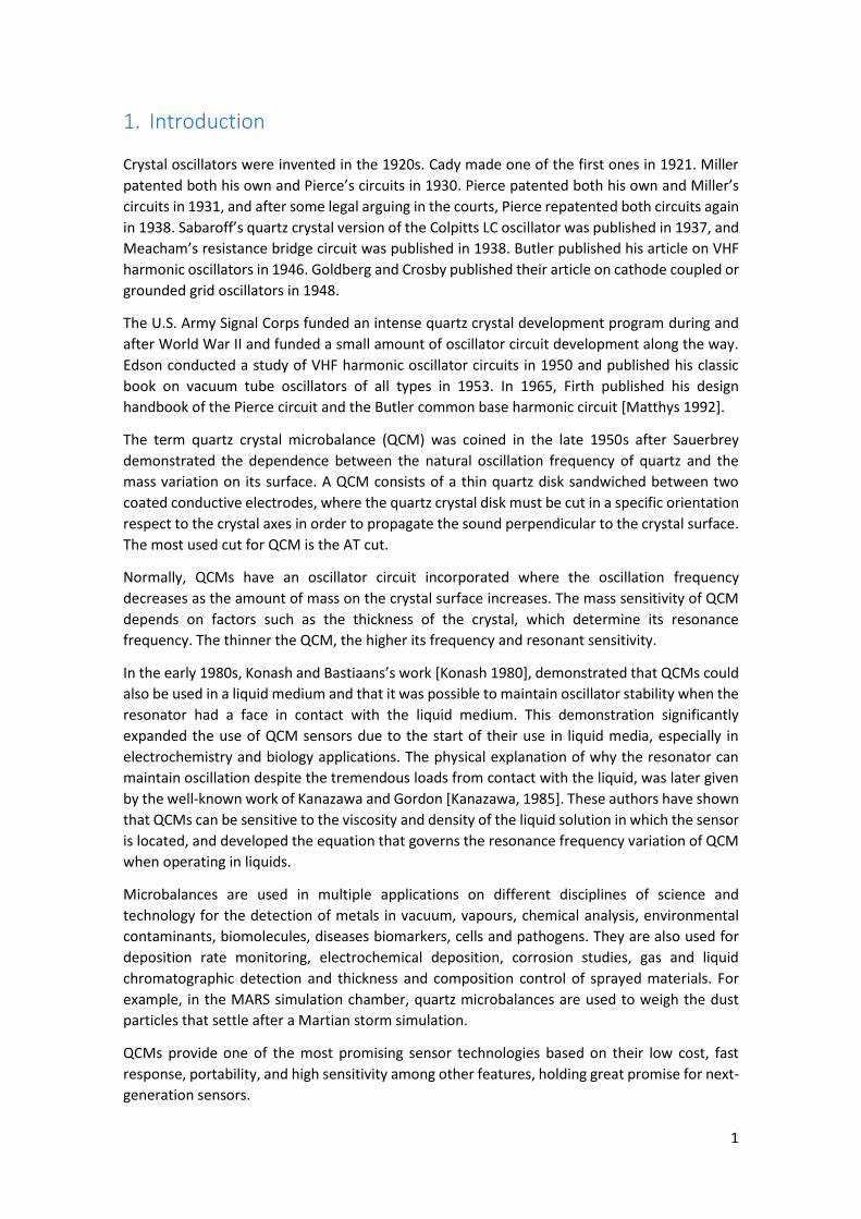
Where N: constant that for the AT cut has a value of 1660 kHz·mm d: disc thickness (mm)
The most notable advantage of the AT cut over other cuts is the stability of the frequency despite
to the variation in temperature. They are related by the equation (2) [Mascareñas 1993] .
∆𝑓
𝑓= 𝐴1 · (𝑇 − 𝑇𝑟𝑒𝑓) + 𝐴2 · (𝑇 − 𝑇𝑟𝑒𝑓)
2+ 𝐴3 · (𝑇 − 𝑇𝑟𝑒𝑓)
3
(2)
This equation describes a cubic parabola with an inflection point between 25°C and 35°C,
depending on the shape and frequency of the crystal. In the Figure 4 it can be seen the
temperature curves of an AT cut crystal.
Figure 4: Temperature curve of an AT cut crystal [IDQ 2015]
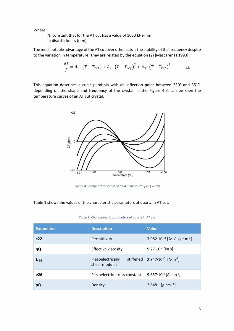
Table 1 shows the values of the characteristic parameters of quartz in AT cut.
Table 1: Characteristic parameters of quartz in AT cut
Parameter Description Value
ε22 Permittivity 3.982·10-11 [A2·s4·kg-1·m-3]
ηQ Effective viscosity 9.27·10-3 [Pa·s]
𝑪𝟔𝟔 Piezoelectrically stiffened
shear modulus 2.947·1010 [Nm-2]
e26 Piezoelectric stress constant 9.657·10-2 [A·s·m-2]
ρQ Density 2.648 [g·cm-3]

6
The quartz resonator is made up of a thin AT-cut quartz crystal disk to which two metal electrodes (of chemically inert material, for example gold) are attached on their parallel faces for stimulation and sensing. These electrodes act as electromechanical transducers, that is, if an alternating potential difference of the same frequency as the resonant frequency of the crystal is applied between the electrodes, an alternating electric field is created in the thickness direction. This induces a standing acoustic wave perpendicular to the quartz surfaces, the displacements of particles being transverse to the direction of propagation, and therefore parallel to said surfaces.
The dimension and geometry of the crystal and the electrodes are decisive in the functional characteristics of the resonator. A circular geometry in the electrodes gives better results than the annular one, while increasing its thickness reduces the sensitivity. Another characteristic of the electrode geometry is that reducing its diameter improves the separation of the spurious crystal vibration modes from the fundamental one.
The maximum displacement for the different resonance modes occurs on the crystal surfaces, which makes the device very sensitive to surface disturbances. The frequency of the crystal depends as much on its physical properties as on the properties of the adjacent medium. Figure 5 shows a 9 MHZ AT cut quartz resonator.
Figure 5: Inficon 1 in. Diameter crystals. Electrode configuration
The Butterworth Van-Dyke equivalent circuit (BVD) is used to simulate the electrical properties of the crystal. As seen in Figure 6, this model consists of two branches: the dynamic branch, formed by Cq, Rq and Lq, and the static branch formed only by Cp.
Figure 6: Equivalent circuit of a quartz crystal. Butterworth Van-Dyke Model
The mass of the resonator corresponds to the dynamic inductance Lq, while its elasticity is represented by the capacitor Cq. The dynamic resistance Rq represents losses: friction between

7
the molecules of the crystal, attenuations caused by the gas that covers the crystal, etc. The parallel static capacity, Cp, represents the capacitor formed by the quartz electrodes in which the crystal acts as a dielectric. Harmonic resonances can be simulated by other series of resonance circuits connected in parallel [Marin 2007].
The electrical elements of the BVD model circuit are calculated with equations (3)-(6) [Cernosek 1998].
𝐶𝑝 =
𝜀22 · 𝐴𝑠
ℎ𝑞 (3)
𝑅𝑞 =
(𝑛 · 𝜋)2 · 𝜂𝑞
8𝐾02 · 𝐶𝑝 · 𝐶66
(4)
𝐶𝑞 =
8𝐾02 · 𝐶𝑝
(𝑛 · 𝜋)2
(5)
𝐿𝑞 =
1
𝜔𝑠2 · 𝐶𝑞
(6)
Where: K0: Lossless effective electromechanical coupling factor n(n=1,3,5…): Harmonic resonance of quartz hq: Thickness of quartz crystal As: Effective area of the electrode surface
ωs=2πfs: Angular frequency of series resonance of the concentrated elements. It can be obtained, approximately, by equation (7) [Cernosek 1998] [Rosembaum 1998].
𝜔𝑠 =1
ℎ𝑞√
𝐶66
𝜌𝑞· √(𝑛𝜋)2 − 8𝐾0
2 (7)
The admittance of the quartz resonator, taking into account the parallel capacity, is given by equation (8). Section 2.2.1 explains how this expression is achieved.
𝑌 =
1
𝑍= 𝑗𝜔𝐶𝑝
∗ +1
𝑍𝑚𝑞
+ 𝑍𝑚𝑚
= 𝐺𝑠 + 𝑗𝐵 (8)
The Nyquist diagram of the resonance admittance is observed in the Figure 7.
Figure 7: Admittance of the quartz resonator in the complex plane and resonance frequencies

8
Following the circle of admittance, in increasing direction, the characteristic frequencies of the resonator are:
Maximum module frequency (fm): frequency for which the admittance module of the quartz resonator is maximum.
Series resonance frequency , (fs), given by the equation (9). It is the frequency for which the real part of the admittance of the quartz resonator is maximum.
𝑓𝑠 =1
2𝜋√
1
𝐿𝑞 · 𝐶𝑞
(9)
Lower null phase frequency (fr): frequency for which the imaginary part of the admittance of the quartz resonator is cancelled for the first time.
Greater null phase frequency (fa): frequency for which the imaginary part of the admittance of the quartz resonator is cancelled for the second time.
Parallel frequency (fp) , given by the equation (10). Frequency for which the real part of the impedance of the quartz resonator is maximum.
𝑓𝑝 =1
2𝜋√
𝐶𝑝 + 𝐶𝑞
𝐿𝑞 · 𝐶𝑞 · 𝐶𝑝
(10)
Minimum module frequency (fn): Frequency for which the modulus of admittance of the quartz resonator is minimum.
By measuring the response of the no-load resonator in a frequency range around the resonance and adjusting the admittance to the obtained model, the values of the BVD equivalent circuit can be determined.
In this work we will use a 9 MHz AT cut crystal from Inficon. To characterize its equivalent circuit, the Agilent E5070B network analyser is used, Table 2 shows the equivalent circuit obtained in air and in water.
Table 2: Characteristic parameters of the crystal equivalent circuit
Rq(Ω) Lq(mH) Cq(fF) Cp(pF) fo(MHz) Q
Air 6.566 6.52244 47.9677 19.8456 8.997836 56156
Distilled water
149.271 6.52553 47.9677 28.1271 8.995755 2470
The quality factor Q of a resonator is defined as the ratio of the resonance frequency and the resonance bandwidth. The quality factor determines the rate of fall of the signal when
excitation is interrupted in a resonator. Figure 8 shows the resonant behaviour of a lossy system.

9
Figure 8: Resonant system with losses. Ratio of bandwidth to quality factor [Tumero 2013]
Narrower the resonance bandwidth is, greater is Q. The quality factor is directly proportional to the time it takes for the signal to decay 1/e of the vibration amplitude it had before stopping the excitation.
Quartz resonators are characterized for a high Q. There are some elements that influence the quality factor such as geometry, material defects, surface finish, harmonics, ionizing radiation, temperature, type of electrodes and the interfering modes. Of course, from the point of view of sensor operation, when a crystal is immersed in a liquid medium or has a deposited mass, or both, the quality factor decreases.
Equation (11) expresses the quality factor of a vacuum resonator as a function of the parameters of the crystal equivalent circuit.
𝑄 =
𝜔𝑠 · 𝐿𝑞
𝑅𝑞 (11)
2.2. Quartz crystal resonator as QCM sensor
One of the applications of quartz crystal resonators is their use as quartz crystal microbalance sensors. It is defined as a microbalance due to the linear relationship between the frequency variation and the mass deposited on the glass [Etchenique 1997].
The AT cut quartz crystal resonator exhibits its highest sensitivity on crystal surfaces. When the characteristics of the crystal environment change, they affect the sensitive area of the resonator and the resonator responds changing its behaviour. This reaction is what turns the quartz resonator into an advanced sensor capable of detecting numerous physical variables, as well as
various processes.
If mass is deposited on the resonator surface, an alteration of the resonance frequency proportional to the amount of added mass occurs. The sensibility of the resonator to the changes in surface mass is very high. But changes in other parameters of the layer deposited, including the visco-elastic properties, can also contribute to the response and therefore should
10
also be considered. The chemical and biological sensitivity of the sensor is achieved by adding a thin selective layer on the resonator surface that acts as a sensitive element. The properties of this layer will change in response to the concentration of the chemical or biological species to be detected. The interaction of the layer with the propagated wave allows the conversion of the chemical magnitude into acoustic.
There are two ways to detect variations in the acustic wave that propagates through the crystal:
Active mode: the sensor is part of an oscillator electronic circuit so that the changes that occur in the acoustic wave are detected as variations in the oscillator's working frequency.
Passive mode: the characteristics of the sensor are measured passively. For this, the sensor is supplied with an external electrical test signal and the response of the sensor to that signal is observed.
In this work, different oscillator topologies of QCM sensors are characterized by observing their behaviour in a gaseous medium by depositing a thin layer of rigid mass, and in a liquid medium, when its physical characteristics (density and viscosity) affect the behaviour of the sensor, allowing detection and measurement of the physical parameter.
2.2.1. Coated quartz crystal
To analyse the sensor as an electronic component within a circuit, it is very useful to represent
the sensor by means of a suitable impedance model. The model that better represents the
resonator impedance response is derived from the Transmission Line Model (TLM) [Cernosek
1998] [Lucklum 1997] [Rosembaum 1998] or from the continuous electromechanical model
where the complex electrical impedance of the loaded QCR resonator is described as indicated
by equation (12).
𝑍 =1
𝑗𝜔𝐶𝑝[1 −
𝐾𝑞2
𝛼𝑞·
2 · 𝑡𝑎𝑛 (𝛼𝑞
2 ) − 𝑗𝑍𝐿𝑍𝑞
1 − 𝑗𝑍𝐿𝑍𝑞
· cot (𝛼𝑞)]
(12)
Where: Kq: Complex electromechanical coupling factor for lossy quartz αq: Complex phase of acoustic wave through lossy quartz ω: angular frequency ZL: Surface load impedance Zq: Characteristic impedance of quartz
The characteristic impedance of quartz is calculated following equation (13).
𝑍𝑞 = √𝑐�� · 𝜌𝑞 (13)
Where cq is the static capacity of the crystal between the electrodes. This value is obtained from
equation (14).
𝑐𝑞 = 𝐶66
+ (𝑒26
2
𝜀22) + 𝑗𝜔𝜂𝑞
(14)

11
It can be seen that the electrical impedance of the coated quartz crystal resonator can be
calculated directly from the crystal parameters, leaving only the surface charge impedance ZL as
the external factor. This would simplify equation (12) for the uncoated glass leaving the equation
as shown.
𝑍 =
1
𝑗𝜔𝐶𝑝[1 −
𝐾𝑞2
𝛼𝑞· 2 · 𝑡𝑎𝑛 (
𝛼𝑞
2)]
(15)
The electrical impedance given in equation (12) can be expressed, without simplifications, as a
parallel circuit formed by a static capacitance, Cp, and a dynamic impedance, Zm, associated with
the electro-mechanical vibration of the sensor.
𝑍 =
1
𝑗𝜔𝐶𝑝//𝑍𝑚 =
𝑍𝑚
1 + 𝑗𝜔𝐶𝑝 · 𝑍𝑚 (16)
Of both equations , (12) and (16), the expression of Zm is obtained as indicated by the equation
(17).
𝑍𝑚 = 𝑅𝑚 + 𝑗 · 𝑋𝑚 =1
𝑗𝜔𝐶𝑝·
[ 1 − 𝑗
𝑍𝐿𝑍𝑞
· cot(𝛼𝑞)
𝐾𝑞2
𝛼𝑞· (2𝑡𝑎𝑛 (
𝛼𝑞
2 ) − 𝑗𝑍𝐿𝑍𝑞
)
− 1
]
(17)
This equation can be divided into two parts as shown in the equation (18).
𝑍𝑚 =1
𝑗𝜔𝐶𝑝
[
𝛼𝑞
𝐾𝑞2
2𝑡𝑎𝑛 (𝛼𝑞
2 )− 1
] +
1
𝜔𝐶0·
𝛼𝑞
4𝐾𝑞2 ·
𝑍𝐿𝑍𝑞
1 −𝑗𝑍𝐿𝑍𝑞
2𝑡𝑎𝑛 (𝛼𝑞
2)
= 𝑍𝑚𝑞
+ 𝑍𝑚𝑚 (18)
The term Zmq represents the dynamic impedance of quartz without load, while Zm
m represents
the contribution of load on dynamic impedance.
Generally, the electrical admittance of a piezoelectric sensor is more used compared to the
impedance. From the equations (16) and (17) the expression (19) is obtained for the
admittance.
𝑌 =
1
𝑍= 𝑗𝜔𝐶𝑝
∗ +1
𝑍𝑚𝑞
+ 𝑍𝑚𝑚
= 𝐺𝑠 + 𝑗𝐵 (19)
Where C*
p=C0+Cp Gs: sensor conductance B: sensor susceptance
C0 corresponds to a capacity external to the quartz crystal, which runs in parallel with Cp. Added
due to cell, encapsulation, cables, connections, etc…

12
The additive character of the dynamic impedance of quartz and the contributions to the global
dynamic impedance of surface charge is accurate within the one-dimensional model and
equation (18) can be applied without restrictions to quartz crystal load (Lucklum, Behling, &
Cernosek, 1997).
For frequencies close to the mechanical resonance frequency, the dynamic impedance Zmq
associated with a resonator without load can be simplified to a series circuit of lumped elements
(LEM, Lumped Element Model) [Arnau 2001] [Bottom 1982] [Cady 1964] [Martin 1991]
[Nwankwo 1998].
𝑍𝑚𝑞
=1
𝑗𝜔𝐶𝑝
[
𝛼𝑞
𝐾𝑞2
2𝑡𝑎𝑛 (𝛼𝑞
2)
− 1
] = 𝑅𝑞 + 𝑗𝜔𝐿𝑞 +
1
𝑗𝜔𝐶𝑞
(20)
The last member of the previous expression describes the dynamic impedance of the BVD equivalent circuit of a resonator without load, described in section 2.1. On the other hand, in equation (18), the contribution of the load on the dynamic impedance of the resonator Zm
m, is expressed as:
𝑍𝑚𝑚 =
1
𝜔𝐶𝑝·
𝛼𝑞
4𝐾𝑞2 ·
𝑍𝐿𝑍𝑞
1 −𝑗𝑍𝐿𝑍𝑞
2𝑡𝑎𝑛 (𝛼𝑞
2 )
(21)
From this expression can be deducted that, due the imaginary part has to be less than one (condition of small superficial charge), the dynamic impedance associated with the charge can be simplified as indicated by equation (22) [Cernosek 1998] [Granstaff 1994].
𝑍𝑚
𝑚 =𝑛𝜋
4𝐾02𝜔𝑠𝐶𝑝
·𝑍𝐿
𝑍𝑞 (22)
This expression corresponds to that of Zmm in the concentrated elements model (LEM). The LEM
is considered adequate to represent a wide variety of real applications of sensors with visco-
elastic loads [Cernosek 1998].
It can be proved that the impedance Zmm can approximate by a series circuit of three elements:
one with a resistive character Rm, another with an inductive character Lm and the third with a
capacitive character Cm. Depending on the nature of the load, contributions are made to one or
more of these elements.
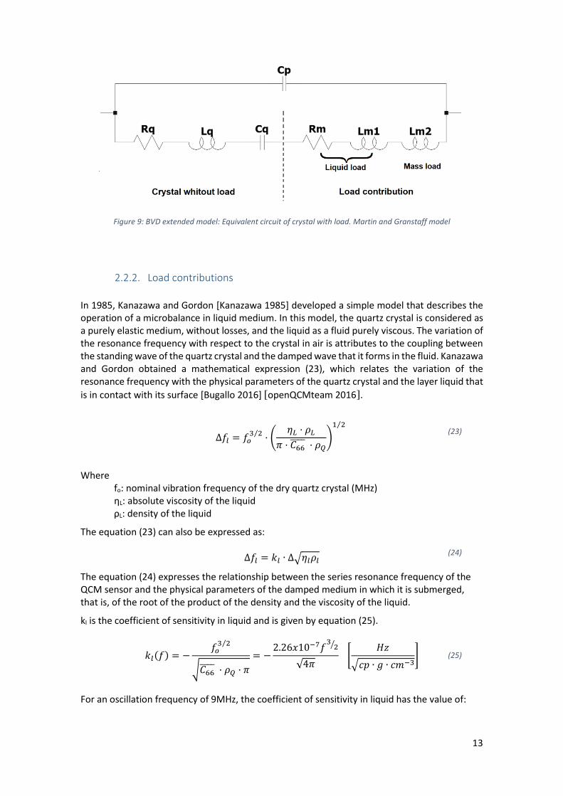
Regarding the operation of the sensor with mass charge, the inductance of the series branch increases proportionally to the density per unit area deposited. On the other hand, when the resonator is submerged in a liquid medium, there is an increase in both the resistance and the inductance of the EQC (Equivalent Quartz Circuit). Figure 9 shows the resulting circuit known as the extended model of the BVD circuit [Martin 1991]. Both contributions, of the mass (Lm2) and that of the liquid medium (Rm, Lm1), are added to the equivalent circuit of the quartz resonator without load (RQ, CQ, LQ).
13
Figure 9: BVD extended model: Equivalent circuit of crystal with load. Martin and Granstaff model
2.2.2. Load contributions
In 1985, Kanazawa and Gordon [Kanazawa 1985] developed a simple model that describes the operation of a microbalance in liquid medium. In this model, the quartz crystal is considered as a purely elastic medium, without losses, and the liquid as a fluid purely viscous. The variation of the resonance frequency with respect to the crystal in air is attributes to the coupling between the standing wave of the quartz crystal and the damped wave that it forms in the fluid. Kanazawa and Gordon obtained a mathematical expression (23), which relates the variation of the resonance frequency with the physical parameters of the quartz crystal and the layer liquid that
is in contact with its surface [Bugallo 2016] [openQCMteam 2016].
Δ𝑓𝑙 = 𝑓𝑜
3 2⁄· (
𝜂𝐿 · 𝜌𝐿
𝜋 · 𝐶66 · 𝜌𝑄
)
1 2⁄
(23)
Where fo: nominal vibration frequency of the dry quartz crystal (MHz)
ηL: absolute viscosity of the liquid ρL: density of the liquid
The equation (23) can also be expressed as:
∆𝑓𝑙 = 𝑘𝑙 ∙ ∆√𝜂𝑙𝜌𝑙 (24)
The equation (24) expresses the relationship between the series resonance frequency of the QCM sensor and the physical parameters of the damped medium in which it is submerged, that is, of the root of the product of the density and the viscosity of the liquid.
kl is the coefficient of sensitivity in liquid and is given by equation (25).
𝑘𝑙(𝑓) = −
𝑓𝑜3 2⁄
√𝐶66 · 𝜌𝑄 · 𝜋
= −2.26𝑥10−7𝑓
32⁄
√4𝜋 [
𝐻𝑧
√𝑐𝑝 ∙ 𝑔 ∙ 𝑐𝑚−3] (25)
For an oscillation frequency of 9MHz, the coefficient of sensitivity in liquid has the value of:
14
𝑘𝑙(𝑓) = −1723 [
𝐻𝑧
√𝑐𝑝 ∙ 𝑔 ∙ 𝑐𝑚−3] (26)
On the other hand, if it is a rigid mass that is deposited on the surface of the crystal, the Sauerbrey equation is used (27) [ (Sauerbrey, 1959)] [Bugallo, 2016].
Δ𝑓𝑚 = −
2𝑓𝑜2
𝐴 · √𝜌𝑄𝐶66
Δ𝑀 (27)
Where fo: nominal vibration frequency of the dry quartz crystal (Hz) ΔM: deposited mass (g)
The equation (27) can also be expressed as:
∆𝑓𝑚 = 𝑘𝑚 ∙ ∆𝑚 (28)
The previous equation expresses the linear relationship between the mass per unit area
(m=M/A) deposited on the surface of the crystal and its resonance frequency. This relationship is given by the mass sensibility coefficient, km, the equation of which results (29):
𝑘𝑚(𝑓) = −
2𝑓𝑜2
√𝐶66 · 𝜌𝑄
= −2.26𝑥10−6 ∙ 𝑓2 [𝐻𝑧
𝑔 ∙ 𝑐𝑚2] (29)
It is observed that the sensibility grows with the frequency in a quadratic way. Therefore, it can increase the sensibility of the sensor by increasing the resonant frequency. However, as the resonant frequency is inversely proportional to the thickness of the crystal, the working frequency will be limited by this: if the frequency is raised too high, the resulting crystal would become extremely fragile. As an example, an AT cut glass with transverse vibration perpendicular to their faces at 9 MHz will have a thickness of 190 μm. It sensibility coefficient would be:
𝑘𝑚(𝑓) = −183 [
𝐻𝑧
𝜇𝑔 ∙ 𝑐𝑚2] (30)
From the point of view of the analysis of the equivalent circuit, the variation in frequency is due to the increase in dynamic impedance, which causes modifications in the elements of the equivalent circuit of the crystal, as already mentioned in the section 2.2.1. As can be seen in
Figure 9, introducing the crystal in liquid supposes an increase of the inductance Lq and the resistance Rq. These increases are represented by Rm and Lm1.
The equations that relate the parameters Rm and Lm1 with the properties of the liquid are the following, (31) y (32), [Martin 1991].
𝑅𝑚 =𝜔𝑜𝐿𝑞
𝜋((
2𝜔𝑜𝜂𝐿𝜌𝐿
𝐶66 𝜌𝑄
))
1 2⁄
(31)

15
𝐿𝑚1 =𝜔𝑜𝐿𝑞
𝜋((
2𝜂𝐿𝜌𝐿
𝐶66 𝜌𝑄𝜔𝑜
))
1 2⁄
(32)
On the other hand, the deposition of mass on the crystal surface causes an increase in the
inductance of the crystal that follows the equation (33).
𝐿𝑚2 =2𝜔𝑜𝐿𝑞𝜌𝑠
𝜋((
1
𝐶66 𝜌𝑄
))
1 2⁄
(33)
16
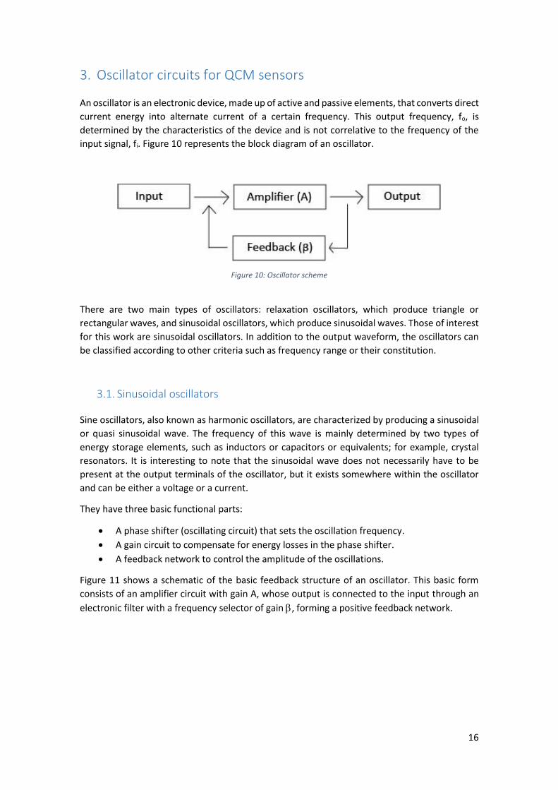
3. Oscillator circuits for QCM sensors
An oscillator is an electronic device, made up of active and passive elements, that converts direct
current energy into alternate current of a certain frequency. This output frequency, fo, is
determined by the characteristics of the device and is not correlative to the frequency of the
input signal, fi. Figure 10 represents the block diagram of an oscillator.
Figure 10: Oscillator scheme
There are two main types of oscillators: relaxation oscillators, which produce triangle or
rectangular waves, and sinusoidal oscillators, which produce sinusoidal waves. Those of interest
for this work are sinusoidal oscillators. In addition to the output waveform, the oscillators can
be classified according to other criteria such as frequency range or their constitution.
3.1. Sinusoidal oscillators
Sine oscillators, also known as harmonic oscillators, are characterized by producing a sinusoidal
or quasi sinusoidal wave. The frequency of this wave is mainly determined by two types of
energy storage elements, such as inductors or capacitors or equivalents; for example, crystal
resonators. It is interesting to note that the sinusoidal wave does not necessarily have to be
present at the output terminals of the oscillator, but it exists somewhere within the oscillator
and can be either a voltage or a current.
They have three basic functional parts:
A phase shifter (oscillating circuit) that sets the oscillation frequency.
A gain circuit to compensate for energy losses in the phase shifter.
A feedback network to control the amplitude of the oscillations.
Figure 11 shows a schematic of the basic feedback structure of an oscillator. This basic form
consists of an amplifier circuit with gain A, whose output is connected to the input through an
electronic filter with a frequency selector of gain , forming a positive feedback network.

17
Figure 11: Oscillator scheme
The conditions for a sinusoidal oscillator to work are known as the Barkhausen criterion.
The first condition is that the modulus of the loop gain is equal to unity (|A·β|=1). To calculate this gain it is necessary open the loop at some point, apply a signal and measure the signal obtained by turning the loop.
The second implies that the feedback signal is in phase. For this, it is necessary shift it 360˚. Since a typical amplifier produces a signal reversal, the feedback circuit must shift the signal only 180˚ (phase A·β=2·k·π).
In the Figure 12, the different types of output wave can be observed according to the value of
the product A · β. In case of the feedback signal is in phase, but at A· β <1, the circuit not oscillate.
If the value of A · β is very close to 1 and a step or impulse is applied to it, a damped oscillation
could be observed. If, on the contrary, A · β> 1, if an oscillation is generated that will grow
exponentially. This oscillation will stop growing as soon as the transistor enters in break or
saturation, leaving the signal cropped.
Figure 12: a) Increasing output, A·β>1 b)Damped output, A·β<1 c)Stable output, A·β=1
3.1.1. RC Oscillators
These oscillators produce a phase shift by resistance-capacitor cells. They are usually used for
low frequency. A basic diagram of the cell is shown in Figure 13. The input Vi represents the
output of the amplifier while Vf is the voltage that is feedback.

18
Figure 13: Schematic of an RC cell
Its operation is based on the phase shift of the current with respect to the input voltage. This
offset is the frequency dependent angle of the input signal and the R and C components. It can
be calculated with the equation (34).
𝜑 = 𝑎𝑟𝑐𝑡𝑔𝑋𝑐
𝑅= 𝑎𝑟𝑐𝑡𝑔
1
2𝜋 · 𝑓 · 𝑅 · 𝐶
(34)
In practice, the phase displacement produced by a capacitor does not reach 90˚. To obtain a
180˚ shift, several cells are joined to add their shifts. At least 3 cells are needed where each
one shifts 60˚. Substituting in equation (35) we obtain the expression of the oscillation
frequency for a basic cell of 60˚ shift.
𝑓 =1
2𝜋 · √3 · 𝑅 · 𝐶
(35)
Figure 14 shows a scheme of how this union would be formed. The value of the three resistors
must be the same as the value of the three capacitors.
Figure 14: Scheme of three RC cells union
The oscillation frequency causes the 180˚ phase shift in the network. With a network analysis it
is extracted that the gain of the feedback network is the one shown in equation (36).
𝛽|𝑓𝑜 =𝑉𝑓
𝑉𝑖=
(𝜔𝑅𝐶)3
(𝜔𝑅𝐶)3 − 5𝜔𝑅𝐶 − 𝑗[6(𝜔𝑅𝐶)2 − 1]
(36)
Since the amplifier can only have a phase shift of 0˚ or 180˚, in the oscillation frequency the
quotient of equation (36) cannot have an imaginary part. To meet this requirement, 6(ωRC)2=1.
From here the equations (37) y (38) are obtained.

19
𝑓𝑜 =1
2𝜋√6 · 𝑅 · 𝐶
(37)
𝛽|𝑓𝑜 =
𝑉𝑓
𝑉𝑖= −
1
29
(38)
There is a dual network of the one shown where resistors and capacitors exchange their
positions. The same attenuation and the frequency shown in equation (39) are obtained in such
network.
𝑓𝑜 =
√6
2𝜋 · 𝑅 · 𝐶
(39)
In both cases the amplifier must have a gain of value -29.
3.1.2. LC oscillators
The operation of the L-C oscillators is based on the use of a resonant circuit. They are often used
at high frequencies. The resonant circuit is composed of three impedances. For the resonance
effect to appear, there must be positive and negative reactance signs, that is, there must be
inductors and capacitors. The oscillation frequency of this type of oscillators is given by equation
(40).
𝑓𝑜 =1
2𝜋 · √𝐿 · 𝐶
(40)
Figure 15.a shows the schematic of a generic three-reactor oscillator. "A" represents a common
emitter transistor. The open loop circuit is shown in Figure 15.b.
Figure 15: a) Schematic of an oscillator b) Schematic of an open-loop oscillator
The impedance Zs is added to incorporate the effect of the beta network output resistance.
𝑍𝑠 = 𝑍2||(𝑍1 + 𝑍3) (41)
𝑍𝑠 =𝑍2 · (𝑍1 + 𝑍3)
𝑍1 + 𝑍2 + 𝑍3
(42)
The amplifier load impedance follows the equation (43).

20
𝑍𝐿 = 𝑍3||(𝑍1 + 𝑍2) (43)
𝑍𝐿 =𝑍3 · (𝑍1 + 𝑍2)
𝑍1 + 𝑍2 + 𝑍3 (44)
The voltage V3 is expressed in equation (45).
𝑉3 = −ℎ𝑓𝑒 · 𝐼𝐵 · 𝑍𝐿
𝑍2
(𝑍1 + 𝑍2)
(45)
Where:
𝐼𝐵 =𝑉1
𝑍𝑠 + ℎ𝑖𝑒
(46)
Substituting equation (45) in (46) the equation (47) is obtained .
𝑉3 =−ℎ𝑓𝑒 · 𝑍𝐿 · 𝑍2 · 𝑉1
(𝑍1 + 𝑍2) · (𝑍𝑠 + ℎ𝑖𝑒)
(47)
And substituting equation (47) with the equations (42) y (44) would be the voltage V3 as the expression (48) shows .
𝑉3 =
−ℎ𝑓𝑒 · 𝑍2 · 𝑉1 ·𝑍3 · (𝑍1 + 𝑍2)𝑍1 + 𝑍2 + 𝑍3
(𝑍1 + 𝑍2) ·𝑍2 · (𝑍1 + 𝑍3)𝑍1 + 𝑍2 + 𝑍3
+ ℎ𝑖𝑒)
(48)
Simplifying equation (48) would be as:
𝑉3 =−ℎ𝑓𝑒 · 𝑍3 · 𝑍2 · 𝑉1
(𝑍1 + 𝑍2 + 𝑍3) · ℎ𝑖𝑒 + 𝑍2 · (𝑍1 + 𝑍3)
(49)
If all three impedances are pure reactive, they can be expressed as Z1=jX1, Z2=jX2 y Z3=jX3. So equation (49) would be:
𝑉3 =−ℎ𝑓𝑒 · 𝑋3 · 𝑋2
𝑗(𝑋1 + 𝑋2 + 𝑋3) · ℎ𝑖𝑒 − 𝑋2 · (𝑋1 + 𝑋3)· 𝑉1
(50)
To fulfill the Barkhausen criterion V3/V1=1 therefore the fraction cannot have an imaginary part. This forces X1+X2+X3=0. This condition eliminates the possibility of using three inductances or three capacitors since positive and negative reactances are needed. Depending on the combination of these elements, they are divided into two families.:
Pierce family: they use two capacitors and one inductance.
Hartley family: they use a capacitor and two inductances.
3.2. Crystal oscillators
A crystal oscillator is a harmonic oscillator whose frequency is determined by a piezoelectric resonator. This frequency is commonly used to control time as in quartz watches, to provide a stable clock signal in digital integrated circuits, and to stabilize the frequencies of radio transmitters and receivers. The most common type of piezoelectric resonator used is quartz

21
crystal, so the oscillators that incorporate them were known as crystal oscillators, but there are other piezoelectric materials such as polycrystalline ceramics that are used in similar circuits.
The oscillators based on the tank circuit do not have great frequency stability due to factors such as temperature, humidity, noise, etc. When high precision is required, quartz crystal is used. The temperature depends on the resonator, but a typical value for quartz crystals is 0.005% of the value at 25 ° C, in the range of 0 to 70 ° C.
The resonance frequency of the sensor is inversely proportional to the thickness of the crystal (h). This parameter determines the wavelengths and the frequencies of the fundamental mode and the harmonics that can be electrically excited in the crystal, since the resonance condition of the device has been n = 1, 3, 5, 7 ... For fundamental mode, typical resonance frequencies range is 5 to 30 MHz, although frequencies up to 150 MHz can be achieved. For higher frequencies, the crystals would work on their harmonics.
These oscillators support a small frequency adjustment by adding a capacitor in series with the resonator, which brings the frequency of the resonator closer to the parallel resonance. To work with the crystal at its fundamental frequency, it is most common to use the parallel frequency. The parallel resonance is several KHz higher than the series resonance. To obtain very high frequencies, the crystal is operated at an odd harmonic frequency, generally the third or fifth. When the crystal is operated at a harmonic frequency, only the series resonance is used.
If it is desired to ensure oscillation at a harmonic frequency, the crystal must be specially
manufactured for this purpose. In the frequency range between the series resonance frequency
and the parallel resonance frequency, the crystal impedance is inductive. Outside that range,
the crystal impedance is capacitive.
Figure 16 shows a crystal oscillator designed to work at the series resonance frequency.
Figure 16: Serial frequency crystal oscillator
The amplifier will oscillate at the series resonant frequency of the crystal, since at that frequency
the crystal impedance is at a minimum and the feedback amplitude is maximum. The resonance
frequency depends only on the crystal, although if the amplifier's phase shift is not exactly 360˚,
the frequency will variate slightly.
A 360˚ phase shift occurs between the base of transistor T1 and the collector of transistor T2. The
collector voltage of transistor T2 is fed back through the crystal XTAL to the base of T1. In order to
achieve low impedance in the XTAL branch, the input impedances of T1 and the output of T2 must
be as small as possible.

22
The output of the system is taken at the emitter of T2 to prevent the external load from
influencing the oscillation frequency. Finally, the function of the CC capacitor is to block the
voltage of the crystal.
Figure 17 shows the diagram of an oscillator circuit prepared to oscillate at the parallel
resonance frequency.
Figure 17: Parallel frequency crystal oscillator
Since the impedance of the crystal in this range is inductive, it can be used instead of the
inductance in an oscillator of the Pierce family. Some crystals are designed so that their nominal
frequency is obtained only when the parallel external capacity has a certain value. Any variation
in the value of this external capacity will produce variations in frequency. The most effective
method of adjusting the oscillator frequency slightly is using a variable capacitor in series with
the crystal. The values of the capacitors C1 and C2 are chosen so that their ratio ensures
oscillation and they have to be much greater than the parasitic capacities of the T1 transistor.
3.2.1. Pierce family
The Pierce family is part of the LC oscillators and is characterized by the distribution of their
impedances, two capacitors and an inductance. It is made up of Pierce, Clapp and Colpitts
oscillators. They are all based on the same configuration where the Z3 inductance is replaced by
a quartz crystal operating in the inductive zone.
The fundamental difference between the three configurations is mainly found in the location of
the earth. In the Pierce oscillator, the ground is in the emitter, in the Colpitts in the collector and
in the Clapp at the base. This difference entails variations both in the way of feeding and in the
way of polarizing the circuit. In a practical circuit, stray capacitances and bias resistors derive
different elements for each of the three configurations, causing the circuits to function
somewhat differently. Figure 18 shows the basic scheme of each type [Parzen 1983].

23
Figure 18: a) Pierce b) Colpitts c) Clapp
These circuits are among the least critical crystal oscillators, and the allowable component
tolerances are generally more than adequate. However, the output power is only moderate.
Each of the circuits can be designed to cover a wide range of crystal frequencies. Despite this, in
the Clapp and Colpitts configurations, much of the stray capacitance appears through the crystal,
limiting high-frequency application to approximately 30MHz.
In Pierce and Clapp oscillators, base bias resistors are found in large capacitors and therefore do
not affect circuit performance. However, in the Colpitts configuration, the bias resistors are
through the crystal and degrade performance at lower frequencies. The Colpitts configuration
is also more susceptible to interferences. These problems can be overcome by using a field effect
transistor for lower frequencies, since in this way gate bias resistors with higher values can be
used.
The Clapp oscillator has a unique disadvantage in that free-running oscillations can occur if an
inductance is used to supply the DC voltage to the collector. This is resolved by putting a fairly
large resistor in series with the inductance or by using just one resistor. However, the resistance
must be kept large as it drifts to the crystal. For this reason, this setting is not recommended for
low supply voltages.
Of the three possible configurations, the Pierce oscillator is generally the simplest and the
Colpitts the most difficult to design. The Pierce oscillator has the disadvantage that one side of
the crystal cannot be grounded, this makes the use of this type of oscillator for QCM sensors
inadvisable as they reduce its field of application, such as in electrochemical applications when
one of the electrodes have to be grounded.
Regarding frequency stability, the Pierce oscillator is generally in the range of 0.0002% to
0.0005%. The Clapp oscillator is slightly inferior to the Pierce and the Colpitts is slightly inferior
to the Clapp in this regard. If an adjustment is not provided to position the crystal exactly at the
desired frequency, there will be additional frequency errors as a result of component
differences.
Table 3 summarizes the three configurations.

24
Table 3: Comparison of Pierce, Colpitts and Clapp configurations
Oscillator type Pierce Colpitts Clapp
Recommended frequency range
100kHz to 20MHz 1MHz to 20MHz 2MHz to 20MHz
Relative frequency stability
High Moderate Moderate to high
Power Output Moderate Moderate Moderate
Waveform Poor at low frequencies, fair to good above 3MHz
Fair to good Fair to good
Ability to operate properly when circuit stray capacitance and inductance are large
Very good Good Good
Ability to operate over a band of frequencies without retuning
High High High
Design difficulty Simple Moderate Moderate
Recommendations
Recommended unless one side of crystal must be grounded
Recommended if Pierce and Clapp cannot be used
Recommended if one side of the crystal must be grounded. Should not be uses with low supply voltages
3.2.1.1. Clapp oscillator
The Clapp oscillator can be considered of as a loaded ground-based amplifier stage with a
feedback loop. The feedback loop has a capacitive tap from which energy is fed back to the
emitter. The signal diagram can be seen in Figure 19. The crystal is represented by two
components that represent its electrical impedance, Re and Xe.
Figure 19: Clapp oscillator signal diagram

25
To analyse the circuit, we assume that the base-emitter capacitance is included in C1, that the
collector-emitter capacitance is included in C2, and that Re << Xe. The input impedance of the
common base amplifier is Zin=1/gm where gm is the transconductance of the transistor. The gain
would be A=gm·ZL where ZL is the collector load impedance. This can be calculated with equation
(51).
𝑍𝐿 =(𝑋1 + 𝑋2)
2
𝑅𝑒 + 𝑔𝑚𝑋12
(51)
Then the gain of the circuit would be expressed as:
𝐴 =𝑔𝑚(𝑋1 + 𝑋2)
2
𝑅𝑒 + 𝑔𝑚𝑋12
(52)
The voltage ratio of the feedback circuit is given by equation (53).
𝑒1
𝑒2=
𝑋1
𝑋1 + 𝑋2
(53)
The phase angle between the voltages is very small, for practical purposes the voltages e1 and
e2 are considered in phase. With a resistive load, the phase change through the amplifier is zero;
therefore, the phase change throughout the cycle is zero, meeting the phase change
requirements. The requirement for the circuit to oscillate is (𝑒2/𝑒1)𝐴 ≥ 1.
Substituting equations (52) and (53) we obtain equation (54).
(𝑋1
𝑋1 + 𝑋2) [
𝑔𝑚(𝑋1 + 𝑋2)2
𝑅𝑒 + 𝑔𝑚𝑋12 ] ≥ 1
(54)
This can be simplified as:
𝑔𝑚𝑋1𝑋2 ≥ 𝑅𝑒 (55)
This analysis is quite limited by the assumptions made. Also, linear analysis does not provide
information on the output voltage or the crystal unit. In some cases, the Y parameters of the
transistor may not be known, and experimental design techniques must be used.
Some experimental design criteria of the oscillator are:
Capacitors C1 and C2 should be as large as possible while allowing the circuit oscillates
even when the resistance of the quartz crystal equivalent circuit Re increases. If this
results in a Xe reactance less than that required for the specified load, a cut capacitor
can be placed in series with the crystal.
A load can be connected to the Clapp oscillator in several places, but the maximum
voltage will be obtained at the collector. Any impedance connected to this point must
be high. Lower impedance and more moderate voltages can be found at the emitter.

26
3.2.1.2. Colpitts oscillator
The Colpitts oscillator behaves quite differently from the Pierce Oscillator in certain ways. The
most important difference is in the polarization arrangement, which can present problems for
the Colpitts circuit.
Figure 20: Flow diagram of an oscillator with Colpitts topology
R1 and R2 resistors are not completely insignificant for low frequencies and can have various
effects on the circuit. Among these effects, it stands out that it can increase the effective
resistance of the crystal branch, so reducing its Q, in addition to reducing the loop gain. Both of
these problems can be reduced by using field effect transistors (FETs). However, the stability of
the oscillator with varying temperature is somewhat worse with a FET.
The Colpitts oscillator can be considered as an emitter follower with a capacitive feedback
circuit. If the capacitors C1 and C2 are large enough so that the input and output impedances of
the transistor are effectively affected, and if the crystalline resistance Re is small, then the rate
of increase of the feedback circuit follows the equation (56).
𝑒2
𝑒1=
𝑋1 + 𝑋2
𝑋2 (56)
Voltages e1 and e2 are in phase. The load impedance ZL, which is purely resistive, is calculated
with the equation (57).
𝑍𝐿 =
𝑋22
𝑅𝑒 (57)
The total gain of the circuit follows the equation (58).
𝐴 =𝑔𝑚 · 𝑍𝐿
1 + 𝑔𝑚 · 𝑍𝐿
(58)

27
Since ZL is resistive, the phase change through the amplifier is zero, and the phase change of the
entire loop is zero. Oscillation will occur if the loop gain exceeds unity, (𝑒2/𝑒1)𝐴 ≥ 1.
Substituting equations (56) and (58) we are left with the condition as shown by equation (59).
(𝑋1 + 𝑋2
𝑋2) · (
𝑔𝑚 · 𝑍𝐿
1 + 𝑔𝑚 · 𝑍𝐿) ≥ 1 (59)
Simplifying equation (59) we obtain:
𝑔𝑚𝑋1𝑋2 ≥ 𝑅𝑒 . (60)
It can be seen that the oscillation condition is the same as in the Clapp oscillator. All oscillators
in the Pierce family share this equation.
Furthermore, since the crystal must be resonant with the series combination of C1 and C2, the
crystal reactance can be calculated using the equation X1 + X2 + Xe = 0, where Xe is the crystal
reactance. This analysis is quite limited by the assumptions made. Again, linear analysis does not
provide information on the output voltage or the crystal unit.
In some cases, due to ignorance of the Y parameters of the crystal or for other reasons, an
experimental approach is needed to perform the oscillator design. For this approach, the
following guidelines can be used:
Just as for the Clapp oscillator, in general, C1 and C2 should be as large as possible but
still allow the circuit to oscillate two to three times the maximum allowable crystal
resistance. If this causes the crystalline reactance Xe to be smaller than the specified
load capacity, a cut-off capacitor can be placed in series with the crystal.
As gie and goe are the input and output admittances of the transistor respectively, it is
desirable to leave |X2|<< l/goe and |X1|<< l/gie. This minimizes the effect of the
transistor's input and output conductances on the circuit.
Best stability is achieved if C1 and C2 are as large as possible because they eliminate
any change in transistor capabilities.

28
4. Design and characterization of Clapp and Colpitts oscillating
topologies
In this work, the design of two oscillating topologies will be carried out: Clapp and Colpitts. The
starting point will be a base circuit and the necessary adaptations will be made to obtain 9MHz
oscillators [Frerking 1978]. Subsequently they will be characterized by means of simulation in
order to know their response as micro gravimetric sensors and detectors of physical properties
of liquid media such as density (l) and viscosity (l).
4.1. 9 MHz Clapp oscillator
4.1.1. 9 MHz Clapp oscillator circuit
Figure 21 shows the Clapp topology circuit. The function of each of the components is detailed
below:
Resistors R1, R2, R3 and R4 provide adequate bias to the transistor.
In particular, R4 must have a high enough value to avoid free-running oscillations. Some
designs include an RF choke in series with this resistance to minimize these oscillations,
but it is not essential if a high supply voltage is available and the value of R4 is high
enough as is the case with this design.
Capacitors C1 and C2 must have a relatively high value since they contribute to the
stability of the oscillation. The higher their values, the lower their reactance and it is
possible to avoid the RF choke in series with R4
The crystal is represented by the equivalent circuit.
Figure 21: Crystal oscillator with Clapp topology

29
Figure 22 shows the initial values of the circuit. To simulate the quartz crystal, the experimental values of the parameters of the equivalent circuit equivalent in distilled water shown in Table 2 were used. As transistor, the LM3046 was chosen for its availability in the laboratory. The same equivalent circuit will be used in all circuit designs for the job to facilitate comparison. The design adds an inductance in parallel with the crystal to compensate for the effect of the Cp capacitor.
Figure 22: Crystal oscillator with Clapp topology with component values
4.1.2. Oscillation frequency adjustment
For the adjustment and characterization of the oscillator circuits, it was decided to use the
LTspice software from Analog Devices. LTspice is SPICE based analogic electronic circuit
simulation software. Initially distributed by Linear Technology, this free distribution software,
although it does not have a very intuitive environment, its graphical interface allows to easily
create schematics and visualize the obtained signals, among other functions.
Another advantage of LTspice is that the version that is distributed is complete, with no limits
on knots or components as it usually happens in the student or evaluation versions of other
simulation programs. In addition, its installation is very simple and does not consume many
computer resources during simulations. For all the advantages that this software presents a
priori, this tool is used for the simulations of the oscillator circuits of this work.
When simulations of an oscillator circuit are carried out, they must have a time of sufficient duration to achieve the permanent state. Figure 23 shows the result of the simulation of the circuit of Figure 22; a simulation time of 4 ms is used. It can be seen that the circuit does not begin to increase its amplitude at the output until 2.2 ms; at this point it begins to oscillate and increase its amplitude until reaching the permanent regime. Since it is not easy to establish the exact point at which the signal stabilizes, the simulation time is long enough to ensure that the final values are in a permanent state.
Analysis: Transient Parameters: Stop time 4ms / time to start saving data 0ms /maximum time step 1n Command: .tran 0 4m 0 1n

30
Figure 23: Initial transient simulation of the Clapp oscillator
Although it will be explained in greater detail later, in the first simulations that are carried out it
is necessary to take into account the conditions in which the sensor will work and make first
estimates of its operation in damped media (with deposited mass and in liquid media with
different values √𝜂𝑙𝜌𝑙). As explained in section 2.2.2, these conditions affect the inductance and
resistance values of the dynamic branch of the crystal equivalent circuit, so it is necessary to first
estimate the maximum values that these elements will have and check that the circuit oscillates
in these conditions of maximum damping.
Once it has been verified that the circuit oscillates and the time in which it reaches the steady
state is known, the simulations required to be able to correctly visualize the signals of interest
can be outlined.
The LM3046 transistor model is not found in LTspice libraries, there are several methods to
create a new component just like other simulators. In LTspice you can include the spice model
in the schematic with the model statement that defines its behaviour as shown in the Figure 24.
Figure 24: LM3046 transistor spice model
In this topology, the frequency adjustment is performed with the value of the capacitor C2. To find the most appropriate value, a sweep was performed on the C2 value. It should be noted that to obtain a more accurate value, the time fraction of 6 to 9 ms is chosen where the output signal is already stabilized. Figure 25 shows the result of the simulation. Analysis: Transient and parametric
Parameters: Stop time 9ms / time to start saving data 6ms /maximum time step 1n Command: .tran 0 9m 6m 1n / .step param C2 37p 43p 1p
Figure 25: Clapp oscillator output in parametric simulation in C2

31
Fourier transform is performed on the output signal of the circuit to determine the oscillation frequency. This FFT can be seen in Figure 26.
Figure 26: FFT of the oscillator output in parametric simulation in C2
Viewing the results of Figure 26, the final values of the circuit components are established in
Figure 27. This figure also includes the circuit with updated values.
Component Value
R1 10kΩ
R2 2.7kΩ
R3 4.7kΩ
R4 12kΩ
RL 100Ω
C1 330pF
C2 40pF
C3 0.01μF
C4 220pF
C0 11μF
Q1 LM3046
Figure 27: a) Component values b) Circuit with updated values
4.1.3. Characterization with mass charge and in liquid medium
In order to predict the behaviour of the oscillator when a thin layer of mass is deposited on the
crystal electrode, a simulation was performed in the time domain. The Martin and Granstaff
model indicates that a mass charge causes an increase in the series inductance parameter of
value Lm2. To recreate this effect, a parametric sweep of Lq is made with a value for Lq of Lq +

32
Lm2. The simulation starts with a value of 0μg/cm2, corresponding to distilled water without
mass, and each step increases 100μg/cm2. Equation (33) is used to estimate the Lq values.
Analysis: Transient and parametric Parameters: Stop time 9ms / time to start saving data 6ms / maximum time step 1n Command: .tran 0 9m 6m 1n / .step param Lm 6.5255m 6.7114m 0.0266m
Figure 28: Oscillator output in mass deposition simulation
Fourier transform is performed on the output signal of the circuit to determine the oscillation frequency. The graph is shown in Figure 29 and the measured values in Table 4.
Figure 29: FFT of the oscillator output in the mass deposition simulation
Table 4: Values measured in the FFT of the oscillator output in the mass deposition test
ρs(μg/cm2) Lm(mH) fosc(MHz)
0 6.5255 8.9998788
100 6.5521 8.9820606
200 6.5786 8.9638182
300 6.6052 8.9455758
400 6.6318 8.9277576
500 6.6583 8.9103636
600 6.6849 8.8921212
700 6.7114 8.8747273
It can be seen in Figure 29 that the oscillation frequency varies linearly with the mass deposited on the surface of the crystal. From the values in Table 4, the mass sensitivity coefficient obtained
33
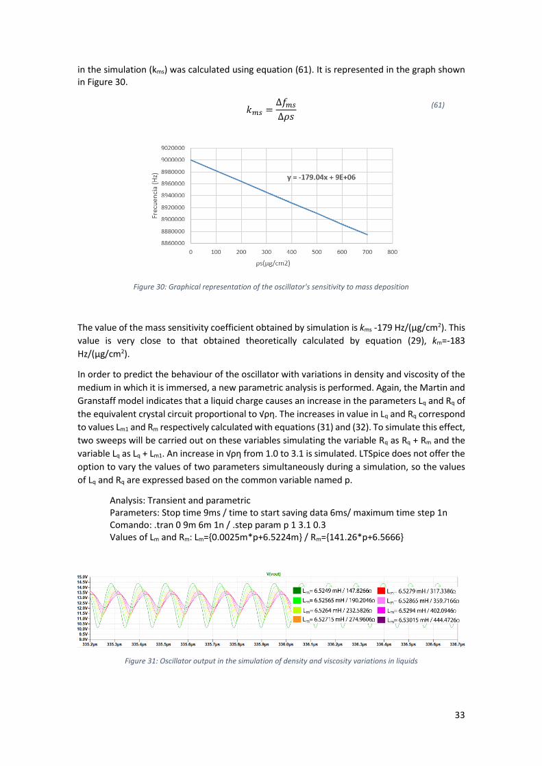
in the simulation (kms) was calculated using equation (61). It is represented in the graph shown in Figure 30.
𝑘𝑚𝑠 =∆𝑓𝑚𝑠
∆𝜌𝑠
(61)
Figure 30: Graphical representation of the oscillator's sensitivity to mass deposition
The value of the mass sensitivity coefficient obtained by simulation is kms -179 Hz/(μg/cm2). This
value is very close to that obtained theoretically calculated by equation (29), km=-183
Hz/(μg/cm2).
In order to predict the behaviour of the oscillator with variations in density and viscosity of the
medium in which it is immersed, a new parametric analysis is performed. Again, the Martin and
Granstaff model indicates that a liquid charge causes an increase in the parameters Lq and Rq of
the equivalent crystal circuit proportional to √ρη. The increases in value in Lq and Rq correspond
to values Lm1 and Rm respectively calculated with equations (31) and (32). To simulate this effect,
two sweeps will be carried out on these variables simulating the variable Rq as Rq + Rm and the
variable Lq as Lq + Lm1. An increase in √ρη from 1.0 to 3.1 is simulated. LTSpice does not offer the
option to vary the values of two parameters simultaneously during a simulation, so the values
of Lq and Rq are expressed based on the common variable named p.
Analysis: Transient and parametric Parameters: Stop time 9ms / time to start saving data 6ms/ maximum time step 1n
Comando: .tran 0 9m 6m 1n / .step param p 1 3.1 0.3 Values of Lm and Rm: Lm={0.0025m*p+6.5224m} / Rm={141.26*p+6.5666}
Figure 31: Oscillator output in the simulation of density and viscosity variations in liquids
34
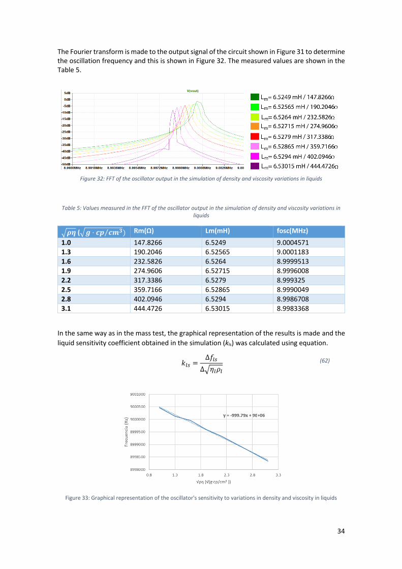
The Fourier transform is made to the output signal of the circuit shown in Figure 31 to determine the oscillation frequency and this is shown in Figure 32. The measured values are shown in the Table 5.
Figure 32: FFT of the oscillator output in the simulation of density and viscosity variations in liquids
Table 5: Values measured in the FFT of the oscillator output in the simulation of density and viscosity variations in liquids
√𝝆𝜼 (√𝒈 · 𝒄𝒑 𝒄𝒎𝟑⁄ ) Rm(Ω) Lm(mH) fosc(MHz)
1.0 147.8266 6.5249 9.0004571
1.3 190.2046 6.52565 9.0001183
1.6 232.5826 6.5264 8.9999513
1.9 274.9606 6.52715 8.9996008
2.2 317.3386 6.5279 8.999325
2.5 359.7166 6.52865 8.9990049
2.8 402.0946 6.5294 8.9986708
3.1 444.4726 6.53015 8.9983368
In the same way as in the mass test, the graphical representation of the results is made and the
liquid sensitivity coefficient obtained in the simulation (kls) was calculated using equation.
𝑘𝑙𝑠 =∆𝑓𝑙𝑠
∆√𝜂𝑙𝜌𝑙
(62)
Figure 33: Graphical representation of the oscillator's sensitivity to variations in density and viscosity in liquids

35
In this case, the liquid sensitivity coefficient obtained by simulation is kls=-1000
Hz √cp ∙ g ∙ cm−3⁄ . This value is much lower in comparison with the theoretically one calculated
by equation (29), kl=-1723 Hz √cp ∙ g ∙ cm−3⁄
4.1.4. Circuit test and board design
Once the circuit was designed and simulated, the physical implementation of the oscillator was
carried out. First, a circuit assembly was made on the Protoboard, shown in Figure 34, to test its
actual operation.
Figure 34: Clapp oscillator mounting on Protoboard
Measuring the output with a Tektronix TDS 2024C oscilloscope gives an oscillation frequency of
8.99448MHz (Figure 35).

36
Figure 35: Output of Clapp oscillator mounted on Protoboard
The next step was the design of the printed circuit board (PCB). The oscillator must incorporate
a temperature sensor in order to know this parameter during the oscillator operation for
compensation or characterization effects. Using the LM35DZ temperature sensor, Figure 36
shows the final design of the board with the built-in temperature sensor as well as a voltage
divider to obtain the 5V of power it requires.
Figure 36: Clapp Oscillator with voltage divider for LM35D7
The design was made using the EasyEDA program. Given the simplicity of the circuit, it is not
necessary to use both sides of the board. Figure 37 shows the upper face of the board where it
can be seen the interconnections of elements, as well as the outputs and inputs to the circuit
designed for the physical model.

37
Figure 37: Clapp Oscillator PCB Design
4.2. 9 MHz Colpitts oscillator
4.2.1. 9 MHz Colpitts oscillator circuit
Figure 38 shows the circuit with Colpitts topology. Next, the function of each of its components
is explained:
Resistors R1, R2 and R3 provide adequate polarity to the transistor.
Capacitors C1 and C2 must have the highest value since they contribute to the stability
of the oscillation eliminating any possible change in the transistor capacitances. In
addition, they minimize the shunt effect of R1 and R2.
The crystal is represented by its equivalent circuit.
Figure 38: Crystal oscillator with Colpitts topology

38
The initial values of the circuit are shown in Figure 39. The LM3046 transistor is also chosen for its availability in the laboratory.
Figure 39: Colpitts crystal oscillator with implemented values
4.2.2. Frequency adjustment
Figure 40 shows the result of the simulation of the circuit of Figure 39. Again, it is observed that
the circuit does not reach the steady state immediately, but until approximately 2.5 ms it does
not begin to oscillate and increase its amplitude. Therefore, in subsequent simulations, a long
time is chosen to ensure that the final values are stabilized.
Analysis: Transient Parameters: Stop time 4ms / time to start saving data 0ms /maximum time step 1n Command: .tran 0 4m 0 1n
Figure 40: Initial transient simulation of the Colpitts oscillator
In this topology, the frequency adjustment is performed with the value of the capacitor C2 too.
To find the most appropriate value, a sweep was performed on the C2 value. Although the design
initially indicated a C2 value between 100pF and 121pF, after some tests it is considered
necessary to lower this value to achieve oscillation despite the increase in resistance in the
crystal equivalent circuit due to added loads.
Analysis: Transient and parametric Parameters: Stop time 12ms / time to start saving data 8ms /maximum time step 1n

39
Command: .tran 0 12m 8m 1n/ .step param C2 30p 50p 5p
Figure 41: Oscillator output in parametric simulation at C2
Fourier transform is performed on the output signal to determine the oscillation frequency of the circuit.
Figure 42: FFT of the oscillator output in parametric simulation in C2
Seeing the results of Figure 42, the value of C2=40pF is chosen. The table in Figure 43 shows the
values of the circuit components. This figure also includes the circuit with the updated values.
Figure 43: a) Component values b) Circuit with updated values

40
4.2.3. Characterization with mass charge and in liquid medium
For the characterization of the circuit before the deposition of mass in the electrode, the same
simulation is carried out explained in section 4.1.3.
Analysis: Transient and parametric Parameters: Stop time 12ms / time to start saving data 8ms / maximum time step 1n Command: .tran 0 12m 8m 1n/ .step param Lm 6.5255m 6.7114m 0.0266m
Figure 44: Oscillator output in mass deposition simulation
Fourier transform is performed on the output signal of the circuit to determine the oscillation frequency. The measured values are collected in Table 6.
Figure 45: FFT of the oscillator output in mass deposition simulation
Table 6: Values measured in the FFT of the oscillator output in the mass deposition test
ρs(μg/cm2) Lm(mH) fosc(MHz)
0 6.5255 9.0002886
100 6.5521 8.9817221
200 6.5786 8.9635074
300 6.6052 8.945956
400 6.6318 8.9278139
500 6.6583 8.9100205
600 6.6849 8.8922626
700 6.7114 8.8748507

41
Just like on the Clapp oscillator, the oscillation frequency varies linearly with the mass deposited
on the surface of the crystal. From the values in Table 6, the mass sensitivity coefficient obtained
in the simulation was calculated using equation (61)
It is represented in the graph shown in Figure 46.
Figure 46: Graphical representation of the oscillator's sensitivity to mass deposition
The value obtained for the sensitivity factor is is kms=-179 Hz/(μg/cm2). This value is very close
to that obtained theoretically calculated by equation (29), km= -183 Hz/(μg/cm2).
For the characterization of the circuit in liquid medium with different densities and viscosities, a
simulation is made with the characteristics explained in the section 4.1.3 (Figure 56).
Analysis: Transient and parametric Parameters: Stop time 12ms / time to start saving data 8ms / maximum time step 1n Command: .tran 0 12m 8m 1n/ .step param p 1 3.1 0.3 Valores de Lm y Rm: Lm={0.0025m*p+6.5224m} / Rm={141.26*p+6.5666}
Figure 47: Oscillator output in the simulation of density and viscosity variations in liquids
The FFT is performed on the output signal of the circuit to determine the oscillation frequency and the results are collected in the Table 7.
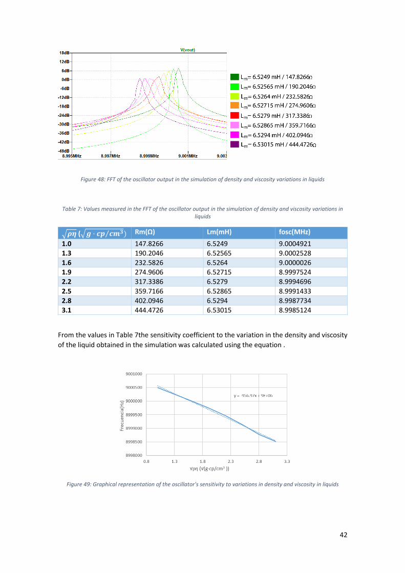
42
Figure 48: FFT of the oscillator output in the simulation of density and viscosity variations in liquids
Table 7: Values measured in the FFT of the oscillator output in the simulation of density and viscosity variations in liquids
√𝝆𝜼 (√𝒈 · 𝒄𝒑 𝒄𝒎𝟑⁄ ) Rm(Ω) Lm(mH) fosc(MHz)
1.0 147.8266 6.5249 9.0004921
1.3 190.2046 6.52565 9.0002528
1.6 232.5826 6.5264 9.0000026
1.9 274.9606 6.52715 8.9997524
2.2 317.3386 6.5279 8.9994696
2.5 359.7166 6.52865 8.9991433
2.8 402.0946 6.5294 8.9987734
3.1 444.4726 6.53015 8.9985124
From the values in Table 7the sensitivity coefficient to the variation in the density and viscosity
of the liquid obtained in the simulation was calculated using the equation .
Figure 49: Graphical representation of the oscillator's sensitivity to variations in density and viscosity in liquids

43
The liquid sensitivity coefficient obtained by simulation is kls=-957 Hz √cp ∙ g ∙ cm−3⁄ . As in the
case of Clapps´s simulation, this value is much lower in comparison with the theoretically one
calculated by equation (29), kl=-1723 Hz √cp ∙ g ∙ cm−3⁄
4.2.4. Board design
The next step was the design of the printed circuit board (PCB). The design was made using the
EasyEDA program. As with the previous design, due to its simplicity, all interconnections can be
made on one side. Figure 50 shows this face of the plate where you can see the interconnections
of elements, as well as the outputs and inputs to the circuit designed for the physical model.
Figure 50: Colpitts Oscillator PCB Design
5. Comparative of the designed topologies with others already
implemented
5.1. Characterization of the topologies already implemented
5.1.1. 9 MHz ABO oscillator
The first person to design an oscillator circuit based on Max Wein's Wein Bridge (1981) was L.A.
Meacham in 1937 to make a high stability oscillator [Meacham 1937]. After this, more oscillator
designs based on the Wein Bridge were made, but modern designs are derived from the William
Hewlett design [Hewlett 1939].
Later, in 1984, Albert Benjaminson designed the Standard Bridge Oscillator (SBO) [Benjaminson
1984]. This design is considered a new topology since it uses double feedback. In addition to the
typical positive of the oscillators, it also uses negative feedback. This produces an increase in
frequency stability and a reduction in phase noise. The disadvantage of this design is that it is

44
necessary to add an automatic gain control to maintain the desired oscillation amplitude. For
this reason, SBO is not used in conventional designs.
The use of the two types of feedback allows defining a new parameter, the MQ factor. This
parameter is called the quartz factor quality multiplier and allows to determine the quality factor
of the quartz crystal loaded by the oscillator circuit. With this parameter, the effect of the
oscillator on the quality factor of the resonator is evaluated numerically and, therefore, on the
short-term frequency stability of the circuit.
In 1996 Kurt O. Wessendorf [Wesendolf 1998] develops the Active Bridge Oscillator topology
(ABO). This design comes from the modification of a Standard Half Bridge Oscillator (SHBO).
Wessendorf found that by biasing a differential pair using a low emitter impedance, Re, instead
of the current source of the SBO, the half-bridge design operates as a standard bridge oscillator
with βp<1. It is a circuit that can be integrate easily and allows working in a wide frequency range.
It provides an alternative with the advantages of bridge oscillators and without the
disadvantages of complexity, design difficulty, high power requirements, and integration.
The Figure 51 shows the schematic circuit of the oscillator and its corresponding equivalent
circuit.
Figure 51: a) ABO schematic b) Equivalent circuit
The ABO oscillator has nonlinearities in its operation in steady state, the amplitude of the large
signal oscillation can be made relatively independent of the resistance of the resonator Rm, Vcc
and temperature changes.
The working points of transistors Q1 and Q2 are similar, however, under oscillation conditions,
the signal amplitudes at the bases are completely different. The base of Q1 has an oscillation
amplitude similar to uo, while the base of Q2 operates at a fraction of the amplitude of the output
signal uo. This allows the gm of each individual transistor to depend heavily on the amplitude of
the signal. When the amplitude increases, 1/gm also increases. Therefore, the magnitude of Av
and βv are in function of the intrinsic emitter resistance re.
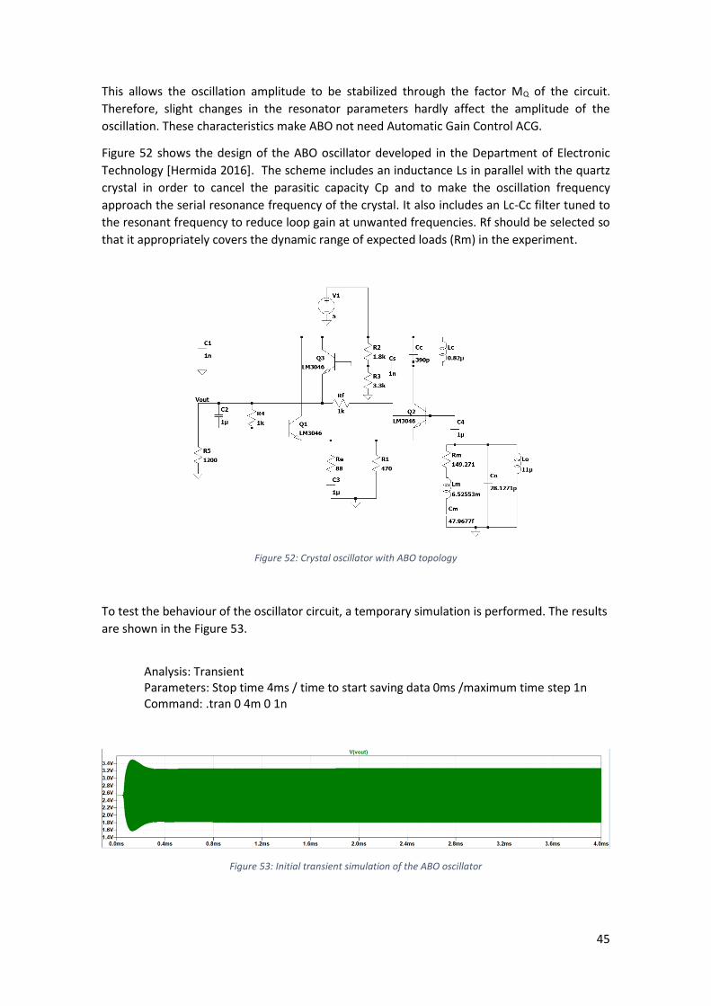
45
This allows the oscillation amplitude to be stabilized through the factor MQ of the circuit.
Therefore, slight changes in the resonator parameters hardly affect the amplitude of the
oscillation. These characteristics make ABO not need Automatic Gain Control ACG.
Figure 52 shows the design of the ABO oscillator developed in the Department of Electronic
Technology [Hermida 2016]. The scheme includes an inductance Ls in parallel with the quartz
crystal in order to cancel the parasitic capacity Cp and to make the oscillation frequency
approach the serial resonance frequency of the crystal. It also includes an Lc-Cc filter tuned to
the resonant frequency to reduce loop gain at unwanted frequencies. Rf should be selected so
that it appropriately covers the dynamic range of expected loads (Rm) in the experiment.
Figure 52: Crystal oscillator with ABO topology
To test the behaviour of the oscillator circuit, a temporary simulation is performed. The results
are shown in the Figure 53.
Analysis: Transient
Parameters: Stop time 4ms / time to start saving data 0ms /maximum time step 1n Command: .tran 0 4m 0 1n
Figure 53: Initial transient simulation of the ABO oscillator

46
As with the Pierce family oscillators, it can be seen that it does not stabilize immediately. In this case, it is observed that the amplitude of the oscillation does not start increasing until it stabilizes as in the Clapp and Colpitts, but rather that it increases and subsequently decreases until its amplitude value stabilizes at 4Vpp.
A new simulation is carried out in a period of time where the stability of the output signal is
ensured to verify operation.
Analysis: Transient Parameters: Stop time 12ms / time to start saving data 8ms /maximum time step 1n Command: .tran 0 12m 8m 1n
Figure 54: ABO oscillator output of transient simulation
FFT is performed on the output signal of the circuit to determine the oscillation frequency (Figure 55).
Figure 55: FFT of the oscillator output in transient simulation
As seen in Figure 55, the adjustment of this oscillator is very precise, being the oscillation
frequency of 8.992MHz.
As with previous oscillators, a parametric analysis of Lm is performed to reproduce the effect of
mass deposition on the electrode. The simulation starts with a value for Lm of 0μg/cm2 and in
each sweep it increases 100μg/cm2. This test is explained in more detail in section 4.1.3.
Analysis: Transient and parametric Parameters: Stop time 12ms / time to start saving data 8ms / maximum time step 1n

47
Command: .tran 0 12m 8m 1n/ .step param Lm 6.5255m 6.7114m 0.0266m
Figure 56: Oscillator output in mass deposition simulation
FFT is performed on the output signal of the circuit to determine the oscillation frequency of
each of the waveforms.
Figure 57: FFT of the oscillator output in mass deposition simulation
The frequency values measured in Figure 57 are shown in Table 8 in correlation with the
corresponding deposited mass.
Table 8: Values measured in the FFT of the oscillator output in the mass deposition simulation
ρs(μg/cm2) Lm(mH) fosc(MHz)
0 6.5255 8.9851497
100 6.5521 8.9671057
200 6.5786 8.949098
300 6.6052 8.9316205
400 6.6318 8.9138484
500 6.6583 8.8961117
600 6.6849 8.8787377
700 6.7114 8.8615611
It can be seen in Figure 57 that the oscillation frequency varies linearly with the mass deposited
on the crystal surface. From the values in Table 8, the mass sensitivity coefficient obtained in
the simulation was calculated using equation .

48
It is represented in the graph shown in Figure 58.
Figure 58: Graphical representation of the oscillator's sensitivity to mass deposition
The value obtained for the sensitivity factor is kms=-176.63 Hz/(μg/cm2). As with the Clapp and
Colpitts topology oscillators, this value is very close to the one obtained theoretically calculated
by equation (29), -183 Hz/(μg/cm2).
To simulate the variation in density and viscosity, the same analysis is performed as in the previous oscillators. This simulation is explained in detail in section 4.1.3.
Analysis: Transient and parametric Parameters: Stop time 12ms / time to start saving data 8ms/ maximum time step 1n Command: .tran 0 12m 8m 1n/ .step param p 1 3.1 0.3 Values of Lm and Rm: Lm={0.0025m*p+6.5224m} / Rm={141.26*p+6.5666}
Figure 59: Oscillator output in simulating density and viscosity variations in liquids
FFT is performed to determine the oscillation frequency to the output signal of the circuit and the results are shown in Table 9.

49
Figure 60: FFT of the oscillator output in the simulation of density and viscosity variations in liquids
Table 9: Values measured in the FFT of the oscillator output in the simulation of density and viscosity variations in liquids
√𝝆𝜼 (√𝒈 · 𝒄𝒑 𝒄𝒎𝟑⁄ ) Rm(Ω) Lm(mH) fosc(MHz)
1.0 147.8266 6.5249 8.9922613
1.3 190.2046 6.52565 8.9917585
1.6 232.5826 6.5264 8.9910175
1.9 274.9606 6.52715 8.9904883
2.2 317.3386 6.5279 8.9897739
2.5 359.7166 6.52865 8.9892448
2.8 402.0946 6.5294 8.9885305
3.1 444.4726 6.53015 8.9880279
Again, from these values the sensitivity coefficient of simulation for the variation of density and
viscosity in liquids is calculated by equation (62). In this case, kls=-2056 Hz √cp ∙ g ∙ cm−3⁄ , this
value is more closer to the theoretical one kl=-1723 Hz √cp ∙ g ∙ cm−3⁄ .
Figure 61: Graphical representation of the oscillator's sensitivity to variations in density and viscosity in liquids
5.1.2. 9 MHz Miller oscillator
The Miller oscillator belongs to the Hartley family of oscillators. The Hartley family began with
the design of the Hartley handheld oscillator Ralph Ralph Vinton Lyon Hartley in 1920. As
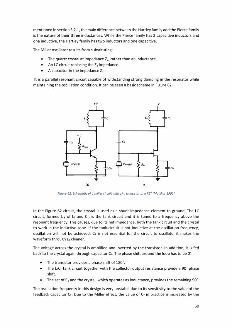
50
mentioned in section 3.2.1, the main difference between the Hartley family and the Pierce family
is the nature of their three inductances. While the Pierce family has 2 capacitive inductors and
one inductive, the Hartley family has two inductors and one capacitive.
The Miller oscillator results from substituting:
The quartz crystal at impedance Z1, rather than an inductance.
An LC circuit replacing the Z2 impedance.
A capacitor in the impedance Z3.
It is a parallel resonant circuit capable of withstanding strong damping in the resonator while
maintaining the oscillation condition. It can be seen a basic scheme in Figure 62.
Figure 62: Schematic of a miller circuit with a) a transistor b) a FET [Matthys 1992]
In the Figure 62 circuit, the crystal is used as a shunt impedance element to ground. The LC
circuit, formed by of L1 and C1, is the tank circuit and it is tuned to a frequency above the
resonant frequency. This causes, due to its net impedance, both the tank circuit and the crystal
to work in the inductive zone. If the tank circuit is not inductive at the oscillation frequency,
oscillation will not be achieved. C1 is not essential for the circuit to oscillate, it makes the
waveform through L1 cleaner.
The voltage across the crystal is amplified and inverted by the transistor. In addition, it is fed
back to the crystal again through capacitor C2. The phase shift around the loop has to be 0˚.
The transistor provides a phase shift of 180˚.
The L1C1 tank circuit together with the collector output resistance provide a 90˚ phase
shift.
The set of C2 and the crystal, which operates as inductance, provides the remaining 90˚.
The oscillation frequency in this design is very unstable due to its sensitivity to the value of the
feedback capacitor C2. Due to the Miller effect, the value of C2 in practice is increased by the

51
value of the transistor base-collector internal capacitance, both values multiplied by the gain of
the transistor. The transistor gain varies with various factors such as temperature. This leads to
the fact that the effective value of C2 is variable and therefore, the oscillation frequency too.
The transistor version (Figure 62.a) will work at high or medium frequencies, but not at low
frequencies. At low frequencies, the resistive load of the base input resistance of the transistor
through the high impedance crystal is so great that the circuit will not be able to oscillate.
Instead, the FET version of the circuit (Figure 62.b) can be used at any frequency: low, medium,
or high. The crystal voltage waveform is much better with a FET than with a transistor. Even so,
the frequency is still unstable and for the same reason: variability in effective feedback
capacitance C2 due to changes in FET gain.
The Figure 63 shows the schematic of the Miller oscillator to be characterized. This design was
developed, optimized, implemented and characterized previously in the Department of
Electronic Technology [Rodríguez-Pardo 2003], [Rodríguez-Pardo 2011].
Figure 63: Oscillator with Miller topology
Oscillator operation is tested using a transient simulation. The result obtained is shown in Figure
64.
Analysis: Transient Parameters: Stop time 4ms / time to start saving data 0ms /maximum time step 1n Command: .tran 0 4m 0 1n
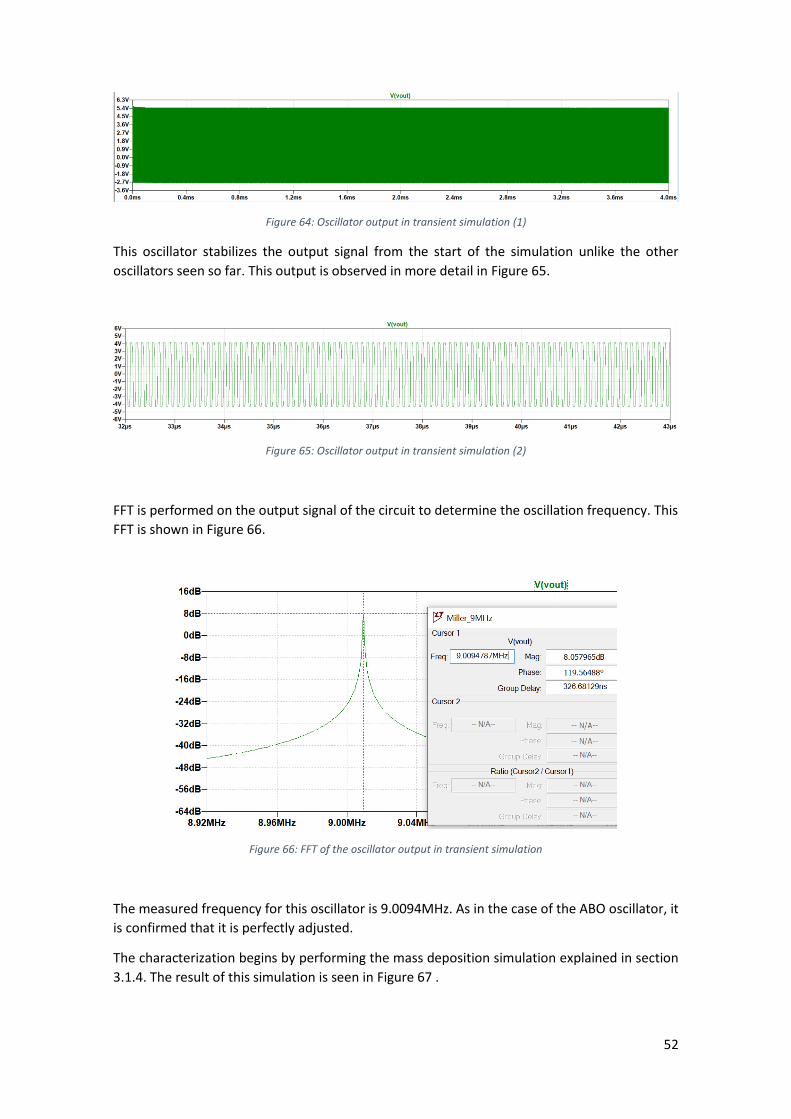
52
Figure 64: Oscillator output in transient simulation (1)
This oscillator stabilizes the output signal from the start of the simulation unlike the other
oscillators seen so far. This output is observed in more detail in Figure 65.
Figure 65: Oscillator output in transient simulation (2)
FFT is performed on the output signal of the circuit to determine the oscillation frequency. This
FFT is shown in Figure 66.
Figure 66: FFT of the oscillator output in transient simulation
The measured frequency for this oscillator is 9.0094MHz. As in the case of the ABO oscillator, it
is confirmed that it is perfectly adjusted.
The characterization begins by performing the mass deposition simulation explained in section
3.1.4. The result of this simulation is seen in Figure 67 .
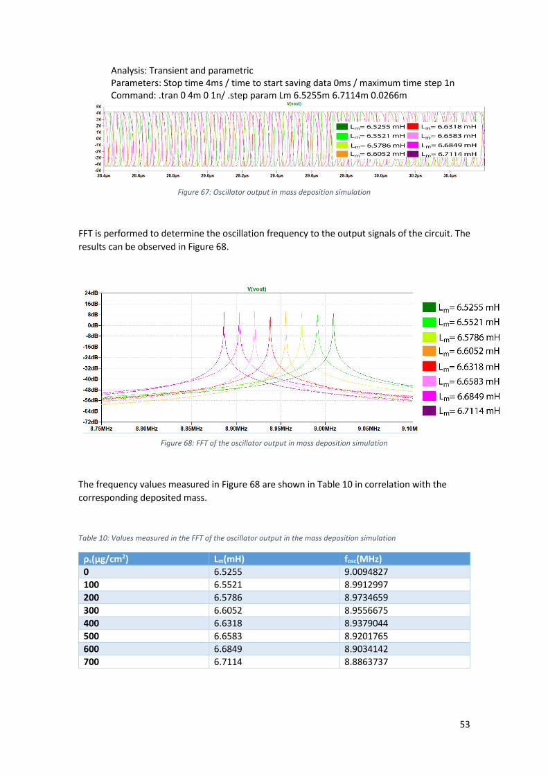
53
Analysis: Transient and parametric Parameters: Stop time 4ms / time to start saving data 0ms / maximum time step 1n Command: .tran 0 4m 0 1n/ .step param Lm 6.5255m 6.7114m 0.0266m
Figure 67: Oscillator output in mass deposition simulation
FFT is performed to determine the oscillation frequency to the output signals of the circuit. The
results can be observed in Figure 68.
Figure 68: FFT of the oscillator output in mass deposition simulation
The frequency values measured in Figure 68 are shown in Table 10 in correlation with the
corresponding deposited mass.
Table 10: Values measured in the FFT of the oscillator output in the mass deposition simulation
ρs(μg/cm2) Lm(mH) fosc(MHz)
0 6.5255 9.0094827
100 6.5521 8.9912997
200 6.5786 8.9734659
300 6.6052 8.9556675
400 6.6318 8.9379044
500 6.6583 8.9201765
600 6.6849 8.9034142
700 6.7114 8.8863737

54
From the values in Table 10, the mass sensitivity coefficient obtained in the simulation is
calculated using equation . The decrease in frequency is observed as the deposited mass
increases.
It is represented in the graph shown in Figure 69.
Figure 69: Graphical representation of the oscillator's sensitivity to mass deposition
The value obtained for the sensitivity factor is 176.05 Hz/(μg/cm2). This value is very close to
that obtained theoretically calculated by equation (29), 183 Hz/(μg/cm2), and it is very similar to
those obtained in the other oscillators.
The next step is simulate the variation in density and viscosity. The same analysis is performed
as in the previous oscillators. This simulation is explained in detail in section 4.1.3.
Analysis: Transient and parametric
Parameters: Stop time 12ms / time to start saving data 8ms/ maximum time step 1n Command: .tran 0 12m 8m 1n/ .step param p 1 3.1 0.3 Values of Lm and Rm: Lm={0.0025m*p+6.5224m} / Rm={141.26*p+6.5666}
Figure 70: Oscillator output in simulating density and viscosity variations in liquids
Fourier transform is performed to determine the oscillation frequency to the output signal of the circuit and the results are shown in Figure 71.
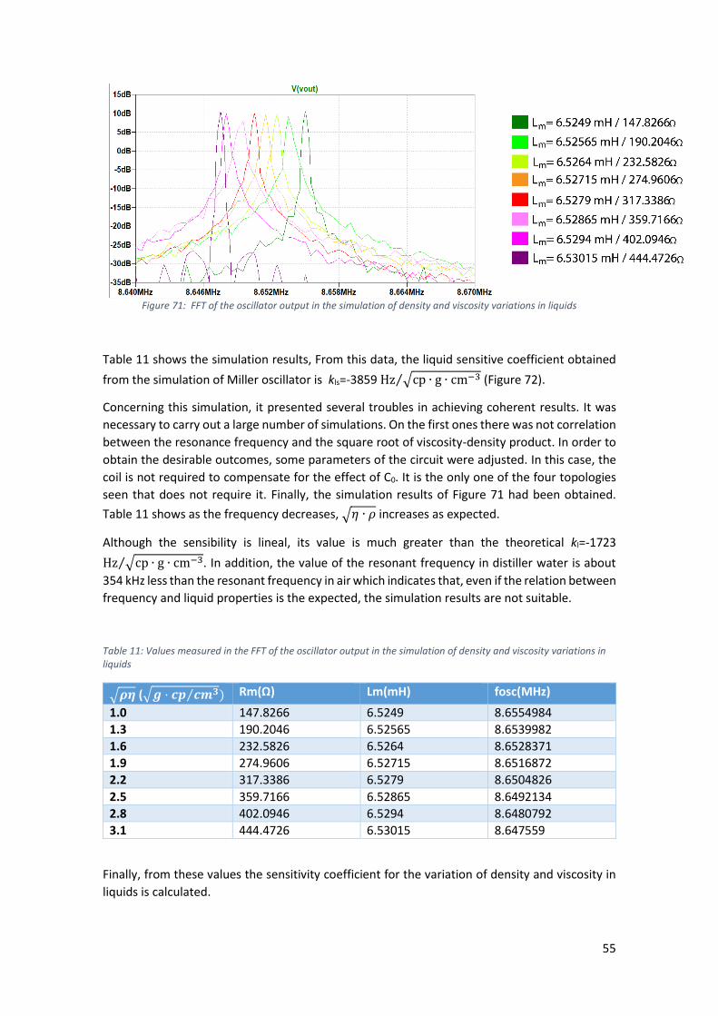
55
Figure 71: FFT of the oscillator output in the simulation of density and viscosity variations in liquids
Table 11 shows the simulation results, From this data, the liquid sensitive coefficient obtained
from the simulation of Miller oscillator is kls=-3859 Hz √cp ∙ g ∙ cm−3⁄ (Figure 72).
Concerning this simulation, it presented several troubles in achieving coherent results. It was
necessary to carry out a large number of simulations. On the first ones there was not correlation
between the resonance frequency and the square root of viscosity-density product. In order to
obtain the desirable outcomes, some parameters of the circuit were adjusted. In this case, the
coil is not required to compensate for the effect of C0. It is the only one of the four topologies
seen that does not require it. Finally, the simulation results of Figure 71 had been obtained.
Table 11 shows as the frequency decreases, √𝜂 ∙ 𝜌 increases as expected.
Although the sensibility is lineal, its value is much greater than the theoretical kl=-1723
Hz √cp ∙ g ∙ cm−3⁄ . In addition, the value of the resonant frequency in distiller water is about
354 kHz less than the resonant frequency in air which indicates that, even if the relation between
frequency and liquid properties is the expected, the simulation results are not suitable.
Table 11: Values measured in the FFT of the oscillator output in the simulation of density and viscosity variations in liquids
√𝝆𝜼 (√𝒈 · 𝒄𝒑 𝒄𝒎𝟑⁄ ) Rm(Ω) Lm(mH) fosc(MHz)
1.0 147.8266 6.5249 8.6554984
1.3 190.2046 6.52565 8.6539982
1.6 232.5826 6.5264 8.6528371
1.9 274.9606 6.52715 8.6516872
2.2 317.3386 6.5279 8.6504826
2.5 359.7166 6.52865 8.6492134
2.8 402.0946 6.5294 8.6480792
3.1 444.4726 6.53015 8.647559
Finally, from these values the sensitivity coefficient for the variation of density and viscosity in
liquids is calculated.

56
Figure 72: Graphical representation of the oscillator's sensitivity to variations in density and viscosity in liquids
5.2. Analysis of the obtained results
Once all four oscillators have been tested, a comparative can be made. To make the comparison
more appropriate, simulations were carried out with the same parameters at each circuits. In
addition, the same equivalent circuit is used for the quartz crystal in all of them.
The first comparison is about the stabilization time of the output signal.
Table 12: Oscillators output signal stabilization time values
Clapp Colpitts ABO Miller
0.7ms 3.1ms 0.3ms 0ms
Seeing at the results of the behaviour simulations of each circuit, it can be seen that the only
one that begins to oscillate as soon as it receives power is the Miller oscillator. Among the other
three models, the fastest to stabilize is the ABO. Although it starts the oscillation in 0.1ms, it is
not until 0.3ms that it stabilizes the amplitude of the output wave. It takes 0.2ms between when
it starts to oscillate and when the output reaches its maximum amplitude. Taking into account
that the output frequency is 9MHz, these 0.3ms would represent 2700 cycles.
Among the remaining two, the fastest to stabilize the output signal is the Clapp oscillator. It
begins to oscillate at 0.4ms, reaching its maximum amplitude at 0.7ms. It would take 0.3ms to
reach it from the start of the oscillation. In this case, the Clapp oscillator would take 3600 lost
cycles before having a stable oscillation.
Finally, the slowest of the models studied is the Colpitts oscillator, with much difference in
stabilization time compared to the others. In this case, the oscillation starts at 2.4ms, achieving
stability 0.7ms later, at 3.1ms from the start. This translates to 27900 cycles.
Regarding the output amplitude, as each of the studied oscillators is supplied with a different
voltage, what is compared is the voltage relationship between the supply voltage and the peak-
peak voltage of the output signal.
Table 13: Values of the relationship between the input voltage and the output voltage (Vout/Vin)
Clapp Colpitts ABO Miller

57
0.291 0.193 0.28 0.81
The best voltage ratio is obtained by the Miller oscillator. With a bipolar input of ± 5V, it gets an
output of 8.1Vpp. It stands out a lot from other three oscillators seen. It is followed by the Clapp
oscillator, which with a 24V supply has an output wave amplitude of 7Vpp.
Very close to the voltage ratio value of the Clapp is the ABO oscillator. In this case the power
supply is 5V and the output wave is 1.4Vpp. Finally, the worst voltage relationship corresponds
to the Colpitts oscillator. It is powered with 15V, but its output wave only has 2.9Vpp.
After comparing their behaviour under normal simulation conditions, the responses to
simulated environmental changes are compared. For the simulation of the variation of mass
deposited on the crystal, the following sensitivity values were obtained.
Table 14: Values of the simulated sensibility coefficient to mass variation (kms) [Hz/(μg/cm2)]
Clapp Colpitts ABO Miller
-179.04 -179.04 -176.63 -176.05
It can be observed that the oscillators of the Pierce family (Clapp and Colpitts) are more sensitive
to mass variation, both obtaining identical sensibility factors. Among the two remaining
topologies, the ABO oscillator obtained the highest sensitivity factor, with the Miller oscillator
being the least sensitive.
It should be noted that the four oscillator models studied obtained a sensibility factor to the
variation of mass deposited on the crystal that was very similar to each other. The theoretical
value of this coefficient calculated for the glass used is km= -183 Hz/(μg/cm2). Although the four
oscillators obtained close values, none reached this sensibility value.
For density and viscosity variation simulations in liquids, the sensitivity values obtained are
shown in the Table 15.
Table 15: Values of the simulated sensitivity coefficient to the variation of density and viscosity in liquids (kls)
[𝐻𝑧 √𝑐𝑝 ∙ 𝑔 ∙ 𝑐𝑚−3⁄ ]
Clapp Colpitts ABO Miller
999.79 956.97 2055.8 3859
The Miller topology oscillator is by far the most sensitive. It is followed in sensibility by the ABO
oscillator. The oscillators of Clapp and Colpitts topologies obtained a similar sensibility
coefficient between them, the most sensitive of both being that of Clapp topology.
The theoretical value of the sensitivity to the variation of density and viscosity of liquids
calculated for the glass used is kl=-1723 Hz √cp ∙ g ∙ cm−3⁄ . The Clapp and Colpitts oscillators
stay well below this sensitivity while the ABO and Miller oscillators far exceed it.
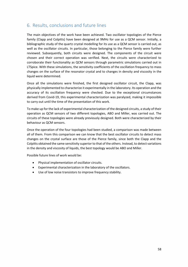
58
6. Results, conclusions and future lines
The main objectives of the work have been achieved. Two oscillator topologies of the Pierce
family (Clapp and Colpitts) have been designed at 9MHz for use as a QCM sensor. Initially, a
bibliographic study of the quartz crystal modelling for its use as a QCM sensor is carried out, as
well as the oscillator circuits. In particular, those belonging to the Pierce family were further
reviewed. Subsequently, both circuits were designed. The components of the circuit were
chosen and their correct operation was verified. Next, the circuits were characterized to
corroborate their functionality as QCM sensors through parametric simulations carried out in
LTSpice. With these simulations, the sensitivity coefficients of the oscillation frequency to mass
changes on the surface of the resonator crystal and to changes in density and viscosity in the
liquid were determined.
Once all the simulations were finished, the first designed oscillator circuit, the Clapp, was
physically implemented to characterize it experimentally in the laboratory. Its operation and the
accuracy of its oscillation frequency were checked. Due to the exceptional circumstances
derived from Covid-19, this experimental characterization was paralyzed, making it impossible
to carry out until the time of the presentation of this work.
To make up for the lack of experimental characterization of the designed circuits, a study of their
operation as QCM sensors of two different topologies, ABO and Miller, was carried out. The
circuits of these topologies were already previously designed. Both were characterized by their
behaviour as QCM sensors.
Once the operation of the four topologies had been studied, a comparison was made between
all of them. From this comparison we can know that the best oscillator circuits to detect mass
changes on the crystal surface are those of the Pierce family, since both the Clapp and the
Colpitts obtained the same sensitivity superior to that of the others. Instead, to detect variations
in the density and viscosity of liquids, the best topology would be ABO and Miller.
Possible future lines of work would be:
Physical implementation of oscillator circuits.
Experimental characterization in the laboratory of the oscillators.
Use of low noise transistors to improve frequency stability.
59
7. Bibliographic references
[AmericanPiezo nd] American Piezo, “Piezoelectricity”, Knowlodge center, without date. URL: https://www.americanpiezo.com/knowledge-center/piezo-theory/piezoelectricity.html
[Arnau 2001]
A. Arnau and Y. Jimenez, “An extended Butterworth-Van Dyke model for quartz crystal microbalance applications in viscoelastic fluid media”, IEEE Trans.Ultrason.Ferroelectr.Freq.Control, 48, (5), pp. 1367- 1382, 2001.
[Benjaminson 1984] A. Benjaminson, “Balanced feedback oscillators”, In proceedings of
the 38 Annual symposium on frequency control, pp. 327-333, 1984.
[BoletinVT 2010]
Boletín VT. “Materiales piezoeléctricos”, Spanish I+D+D Observatory, nº3, Ministry of Science and Education, pp. 1-3, 2010. URL: https://icono.fecyt.es/sites/default/files/filepublicaciones/bvt_mat_n3.pdf
[Bottom 1982] V. E. Bottom, “Introduction to quartz crystal unit design”, Van Nostrand, 1982.
[Bugallo 2016] E. Bugallo Pérez, “Caracterización de la R dinámica en aplicaciones de sensores QCM de medida de masa y medios líquidos”, final degree project, University of Vigo, 2016.
[Cady 1964] W.G. Cady, “Piezoelectricity: an introduction to the theory and applications of electromechanical phenomena in crystals”, New York, 1964.
[Cernosek 1998]
R. W. Cernosek, S. J. Martin, A.R. Hillman and H. L Bandey, “Comparison of lumped-element and transmision-line models for thickness-shear”, IEEE Trans. Ultrason. Ferroelect. Freq. Contr., 45, pp. 1399-1407, 1998.
[Etchenique 1997]
R. Etchenique and E. J. Calvo, “Electrochemical quartz crystal impedance study of redox hydrogel mediators for amperometric enzyme electrodes”, Analytical chemistry, 69, (23), pp. 4833-4841, 1997.
[Frerking 1978] M. Frerking, “Crystal oscillator design and temperture compensation”, Van Nostrand Reinhold, pp. 240-, 1978.
[Granstaff 1994] V. E. Granstaff and S. J. Martin, “Characterization of a thickness-shear mode quartz resonator with multiple nonpiezoelectric layers”, J.Appl.Phys., 3, pp. 1319-1329, 1994.
[Hermida 2016] P. Hermida Costas, “Diseño y caracterización de un circuito electrónico oscilador en puente activo a 9MHz para su utilización

60
como sensor de alta resolución”, final degree project, University of Vigo, 2016.
[Hernández 2011]
J. M. Hernández Lara, “Diseño de un arreglo de 8 sensores de microbalanzas de cuarzo para su aplicación como biosensorde interacciones biomoleculares en líquidos.”, doctoral thesis, University of Veracruz, 2011.
[Hewlett 1939] W. Hewlett, “Variable frequency oscillation generator”, Patent US2268872, United States, 1939.
[IDQ 2015] IDQ, “A short primer on AT-cut quartz crystals”,Blog & Press, 2015. URL: https://www.iqdfrequencyproducts.com/blog/2015/06/29/a-short-primer-on-at-cut-quartz-crystals/
[Kanawaza 1985] K.K Kanazawa and J.G. Gordon, “The Oscillation Frequency of a
Quartz Resonator in Contact with a Liquid”, Analytical Chimical Acta
175, pp. 99-105, 1985.
[Konash 1980] P. L. Konash and G. J. Bastiaans, “Piezoelectric crystal as detectors for liquid chromatography”, Analytical chemistry, 52, pp. 1929-1931, 1980.
[Lucklum 1997] R. Lucklum, C. Behling, R.W. Cernosek, and S. J Martin, “Determination of complex shear modulus with thickness shear mode resonators”, J.Phys.D., 30, pp. 346-356, 1997.
[Marin 2017] J. Marin Garcia, “Extracción de parámetros de un resonador FBAR por optimización“, final degree project, University of Barcelona, 2017.
[Martin 1991]
S.J. Martin, V.E. Grandstaff, G.C. Frye, “Characterization of a quartz
crystal microbalance with simultaneous mass and liquid loading”,
Analytical Chemistry, Vol. 63, pp. 2272‐2281, 1991.
[Mascareñas 1993]
C. Mascareñas and I. Pérez, “Dispositivos piezoeléctricos utilizados en electrónica de radiofrecuencia. Parte A: cristales de cuarzo”, Universidad de Cádiz, Departamento de quimica analitica, pp. 8-12, 1993.
[Matthys 1992] Robert J. Matthys, “Cristal oscillator circuits”, Krieger Malabar revised ed, pp. 24-65, 1992.
[Meacham 1937] L. Meacham, “Stabilized oscillator”, Patent US2163403, United States, 1937.
[Nwankwo 1998] E. Nwankwo and J. Durning, “Impedance response of thicknes-shear mode quartz crystal resonators to contact with linear viscoelastic fluids”, Rev.Sci.Instrum., 69, (6), pp. 2375-2384, 1998.

61
[openQCMteam 2016]
Open QCM, “test of quartz crystal in contact with liquid”, 2016 URL: https://openqcm.com/openqcm-test-of-quartz-crystal-microbalance-in-contact-with-liquid.html
[Montoya 2016] J. F. Montoya and J.D. Salinas, “Sistema para la compensación de temperatura en biosensores piezoeléctricos” . final degree project, EIA university, pp. 20-27, 2016.
[Parzen 1983] B. Parzen, “Design of Crystal and Other Harmonic Oscillators”, Wiley Interscience, pp. 125-168, 181-207, 220-231, 1983.
[Rodríguez-Pardo 2003]
L. Rodríguez-Pardo, “Metodología de diseño de circuitos electrónicos osciladores para la realización de sensores microbalanza de cuarzo en medio líquido”, Doctoral thesis, University of Vigo, 2003.
[Rodríguez-Pardo 2011]
L. Rodriguez-Pardo, A. Cao-Paz, J. Fariña, “Simultaneously measurement of frequency shift and series resistance changes of a quartz resonator using a miller QCM oscillator”, Proceedings of IEEE Sensors, art. no. 6127206, pp. 1054-1057, 2011.
[Rosembaum 1988] J. F. Rosembaum, “Bulk acoustic wave theory and devices”, Artech House Inc, Boston, 1988.
[Sauerbrey 1959] G. Sauerbrey, “Verwendung von Schwingquarzen zur Wägung dünner Schichten und zur Mikrowägung”, Z. Phys., pp. 155-206, 1959.
[Tumero 2013] P. Tumero, “Introducción a los osciladores de cuarzo”, 2013.
[Ugarte 2018] S. Ugarte Ubiergo, “Ultrasonido en emergencias y cuidados críticos”, 2018.
[Wessendorf 1998]
K. O. Wessendorf, "The active-bridge oscillator," Proceedings of the
1998 IEEE International Frequency Control Symposium (Cat.
No.98CH36165), Pasadena, CA, USA, pp. 361-369, doi: 10.1109/FREQ.1998.717929, 1998.