DESIGN AND ANALYSIS OF POWER EFFICIENT SENSE AMPLIFIER ... · this work, we extensively studied the...
14
INTERNATIONAL JOURNAL OF RESEARCH IN COMPUTER APPLICATIONS AND ROBOTICS www.ijrcar.in Vol.2 Issue.2, Pg.: 60-73 February 2014 A.Selvapandian Page 60 INTERNATIONAL JOURNAL OF RESEARCH IN COMPUTER APPLICATIONS AND ROBOTICS ISSN 2320-7345 DESIGN AND ANALYSIS OF POWER EFFICIENT SENSE AMPLIFIER BASED FLIP FLOP Mr. A.Selvapandian, Assistant Professor/ECE PSNA College of Engineering and Technology, Dindigul [email protected] 1 ABSTRACT: - In digital VLSI system the clock distribution network and flip flops are most power consuming components. The reduction of power consumption by clock distribution networks & flip flop makes the total VLSI system as low power VLSI system. In the earlier VLSI system design, different power consumption methods are followed to design the various flip-flops .The SABFF(sense amplifier based flip flop) is one of the types of flip flops in digital VLSI system. The SABFF consists of pulse generator, sensing stage(frontend),latching stage(backend).In previous sense amplifier based flip flops, the sensing stage(frontend) is focused more to make the flip flop as low power consuming element. The proposed work is to design power efficient sense amplifier based flip flop by focusing the sensing stage. The various analyses on the sense amplifier based flip flop is carried out by changing the different sensing stages such as Current mirror sense amplifier (Ct mirror), Full latch sense amplifier. Keywords: SABFF (sense amplifier based flip-flop) Ct mirror(current mirror) INTRODUCTION Integrated circuits were made possible by experimental discoveries which showed that semiconductor devices could perform the functions of vacuum tubes, and by mid-20th-century technology advancements in semiconductor device fabrication. The integration of large numbers of tiny transistors into a small chip was an enormous improvement over the manual assembly of circuits using discrete electronic components. The integrated circuits mass production capability, reliability, and building-block approach to circuit design ensured the rapid adoption of standardized ICs in place of designs using discrete transistors. There are two main advantages of ICs over discrete circuits - cost and performance. Cost is low because the chips, with all their components, are printed as a unit by photolithography and not constructed a transistor at a time. Performance is high since the components switch quickly and consume little power, because the components are small and close together. As of 2006, chip areas range from a few square mm to around 250 mm2, with up to 1 million transistors per mm2. IC design productivity depends on the efficiency with which the design may be converted from concept to architecture, to logic and memory, to circuit and hence to a physical layout.
Transcript of DESIGN AND ANALYSIS OF POWER EFFICIENT SENSE AMPLIFIER ... · this work, we extensively studied the...

INTERNATIONAL JOURNAL OF RESEARCH IN COMPUTER APPLICATIONS AND ROBOTICS www.ijrcar.in
Vol.2 Issue.2, Pg.: 60-73
February 2014
A . S e l v a p a n d i a n
Page 60
INTERNATIONAL JOURNAL OF
RESEARCH IN COMPUTER
APPLICATIONS AND ROBOTICS
ISSN 2320-7345
DESIGN AND ANALYSIS OF POWER EFFICIENT
SENSE AMPLIFIER BASED FLIP FLOP
Mr. A.Selvapandian, Assistant Professor/ECE
PSNA College of Engineering and Technology, Dindigul [email protected] 1
ABSTRACT: - In digital VLSI system the clock distribution network and flip flops are most power consuming
components. The reduction of power consumption by clock distribution networks & flip flop makes the total VLSI
system as low power VLSI system. In the earlier VLSI system design, different power consumption methods are
followed to design the various flip-flops .The SABFF(sense amplifier based flip flop) is one of the types of flip flops
in digital VLSI system. The SABFF consists of pulse generator, sensing stage(frontend),latching stage(backend).In
previous sense amplifier based flip flops, the sensing stage(frontend) is focused more to make the flip flop as low
power consuming element. The proposed work is to design power efficient sense amplifier based flip flop by
focusing the sensing stage. The various analyses on the sense amplifier based flip flop is carried out by changing the different sensing stages such as Current mirror sense amplifier (Ct mirror), Full latch sense amplifier.
Keywords: SABFF (sense amplifier based flip-flop) Ct mirror(current mirror)
INTRODUCTION
Integrated circuits were made possible by experimental discoveries which showed that semiconductor
devices could perform the functions of vacuum tubes, and by mid-20th-century technology advancements in
semiconductor device fabrication. The integration of large numbers of tiny transistors into a small chip was an
enormous improvement over the manual assembly of circuits using discrete electronic components. The integrated
circuits mass production capability, reliability, and building-block approach to circuit design ensured the rapid
adoption of standardized ICs in place of designs using discrete transistors. There are two main advantages of ICs
over discrete circuits - cost and performance. Cost is low because the chips, with all their components, are printed as
a unit by photolithography and not constructed a transistor at a time. Performance is high since the components
switch quickly and consume little power, because the components are small and close together. As of 2006, chip
areas range from a few square mm to around 250 mm2, with up to 1 million transistors per mm2.
IC design productivity depends on the efficiency with which the design may be converted from concept to
architecture, to logic and memory, to circuit and hence to a physical layout.

INTERNATIONAL JOURNAL OF RESEARCH IN COMPUTER APPLICATIONS AND ROBOTICS www.ijrcar.in
Vol.2 Issue.2, Pg.: 60-73
February 2014
A . S e l v a p a n d i a n
Page 61
In many digital very large scale integration (VLSI) designs, the clock system that includes clock
distribution network and flip-flops, is one of the most power consumption components. It accounts for 30% to 60%
of the total system power, where 90% of which is consumed by the flip-flops and the last branches of the clock
distribution network that is driving the flip-flop .With the recent trend in frequency scaling and deep pipelining, this
clocking system power may be even more pronounced. As the power budget of today’s portable digital circuit is
severely limited, it is important to reduce the power dissipation in both clock distribution networks and flip-flops.
Moreover, because of the tight timing budget at high frequency operation, the latency of the flip-flops should be
minimized. Hence, the ability to achieve a design that ensures both power consumption and small latency is essential
in modern VLSI technology. The dual-edge triggering is an important technique to reduce the power consumption in
the clock distribution network.
Dual Edge Triggering
By utilizing dual-edge triggering, the flip-flop is capable of sampling data on both rising and falling edges
of the clock so that only half the clock frequency is needed to obtain the same data throughput of single edge-
triggered flip-flops (SETFFs). Recently, several low-power high-speed DETFF structures have been proposed. In
this work, we extensively studied the operation of existing flip-flop architectures, analysed their weaknesses and
proposed new sense-amplifier based flip-flop circuits (here in after, referred to as a “SAFF” circuit) due to its
differential characteristics, fast operation speed, and low-power consumption. This SAFF circuit is implemented by
various approaches within digital circuits such as microprocessors, digital signal processing units, and the like. The
first flip-flop achieves substantial power reduction by concurrently incorporating dual-edge triggering and
conditional pre charging. It also minimizes the latency by making use of a fast symmetrical latch. By using the first
proposed design as the baseline circuit, a novel clock gating flip-flop circuit is developed to further reduce the power
dissipation and at low input switching activity, the second proposed design promises an even greater amount of
power savings.
SENSE AMPLIFIER
Sense Amplifier is important component of memory design. The choice and design of Sense Amplifier robustness of
bit line sensing impacting read speed and power. Due to variety of Sense Amplifiers in semiconductor memories and
the impact they have on final specs of memory, the sense amplifiers have become a separate class of circuit. Sense
amplifiers play a major role in the functionality Performance and reliability of memory circuits. Sense amplifier
performs a function like amplification, power reduction & delay reduction
In this paper a new method for power reduction by clock distribution networks & flip flop has been proposed and
developed which makes the total VLSI system as low power VLSI system.
This paper has been implemented in low power application in VLSI system to design a flip-flop.
SURVEY OF EXISTING METHODS
LOW-POWER CMOS DESIGN FOR LOW-SWING CIRCUITS
This paper describes some of the circuit level techniques for low-power CMOS designs. VTH control
circuits are necessary for achieving low-threshold voltage in high-speed low-voltage applications. In order to reduce
the clock system power, it is effective to reduce a clock voltage swing. Such idea is embodied in the Reduced Clock
Swing Flip-Flop (RCSFF).
INTERNATIONAL JOURNAL OF RESEARCH IN COMPUTER APPLICATIONS AND ROBOTICS www.ijrcar.in
Vol.2 Issue.2, Pg.: 60-73
February 2014
A . S e l v a p a n d i a n
Page 62
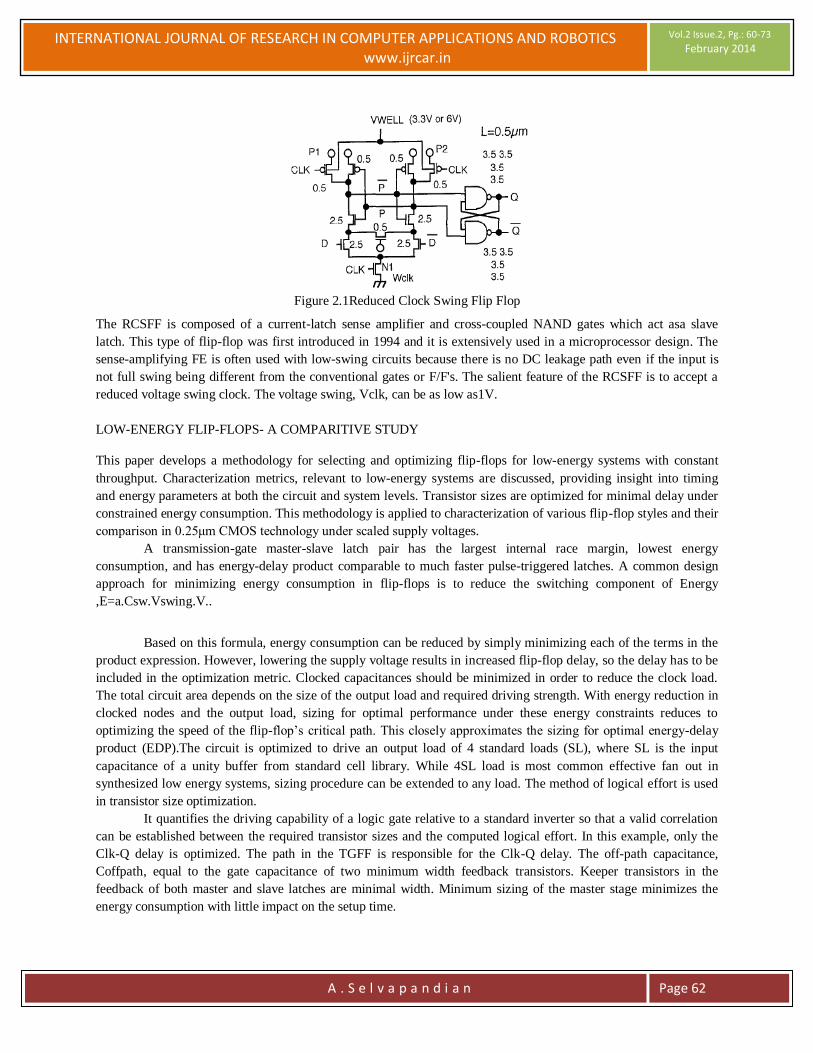
Figure 2.1Reduced Clock Swing Flip Flop
The RCSFF is composed of a current-latch sense amplifier and cross-coupled NAND gates which act asa slave
latch. This type of flip-flop was first introduced in 1994 and it is extensively used in a microprocessor design. The
sense-amplifying FE is often used with low-swing circuits because there is no DC leakage path even if the input is
not full swing being different from the conventional gates or F/F's. The salient feature of the RCSFF is to accept a
reduced voltage swing clock. The voltage swing, Vclk, can be as low as1V.
LOW-ENERGY FLIP-FLOPS- A COMPARITIVE STUDY
This paper develops a methodology for selecting and optimizing flip-flops for low-energy systems with constant
throughput. Characterization metrics, relevant to low-energy systems are discussed, providing insight into timing
and energy parameters at both the circuit and system levels. Transistor sizes are optimized for minimal delay under
constrained energy consumption. This methodology is applied to characterization of various flip-flop styles and their
comparison in 0.25μm CMOS technology under scaled supply voltages.
A transmission-gate master-slave latch pair has the largest internal race margin, lowest energy
consumption, and has energy-delay product comparable to much faster pulse-triggered latches. A common design
approach for minimizing energy consumption in flip-flops is to reduce the switching component of Energy
,E=a.Csw.Vswing.V..
Based on this formula, energy consumption can be reduced by simply minimizing each of the terms in the
product expression. However, lowering the supply voltage results in increased flip-flop delay, so the delay has to be
included in the optimization metric. Clocked capacitances should be minimized in order to reduce the clock load.
The total circuit area depends on the size of the output load and required driving strength. With energy reduction in
clocked nodes and the output load, sizing for optimal performance under these energy constraints reduces to
optimizing the speed of the flip-flop’s critical path. This closely approximates the sizing for optimal energy-delay
product (EDP).The circuit is optimized to drive an output load of 4 standard loads (SL), where SL is the input
capacitance of a unity buffer from standard cell library. While 4SL load is most common effective fan out in
synthesized low energy systems, sizing procedure can be extended to any load. The method of logical effort is used
in transistor size optimization.
It quantifies the driving capability of a logic gate relative to a standard inverter so that a valid correlation
can be established between the required transistor sizes and the computed logical effort. In this example, only the
Clk-Q delay is optimized. The path in the TGFF is responsible for the Clk-Q delay. The off-path capacitance,
Coffpath, equal to the gate capacitance of two minimum width feedback transistors. Keeper transistors in the
feedback of both master and slave latches are minimal width. Minimum sizing of the master stage minimizes the
energy consumption with little impact on the setup time.

INTERNATIONAL JOURNAL OF RESEARCH IN COMPUTER APPLICATIONS AND ROBOTICS www.ijrcar.in
Vol.2 Issue.2, Pg.: 60-73
February 2014
A . S e l v a p a n d i a n
Page 63
CURRENT MIRROR SENSE AMPLIFIER
This paper describes that current mirror sense amplifier has better improvement in the noise immunity and speed of
read circuit. Current Mirror Sense Amplifier takes differential input and amplify them large signal output. The
differential approach presents numerous advantages over single ended counterpart – one of the most important being
common mode rejection. That is such amplifier rejects the noise that is equally injected at both input. The signal
common at both input suppressed at output of amplifier. The drawback is current mirror sense amplifier that it
consumes more power than other type due to dc bias current.
FULL LATCH SENSE AMPLIFIER
The power problem is one of the most serious limitations in the high performance - VLSI's circuits. The
power dissipation of on chip memories and interface circuits occupies a large portion of the total power dissipation.
Full latch sense amplifier consumes less power than other configuration of sense amplifier. Even though the
conventional latch based on two cross coupled inverters is widely used as a sense amplifier, it always requires some
decoupling at its input. This drawback does not occur for the latch circuit shown in fig -3. The most critical point of
latch-type sense amplifiers is that once the decision process has started, it does not recover unless the circuit is reset
to the metastable Due to fast speed, low power consumption, high input impedance and full-swing output latch type
sense amplifier are very attractive for many applications.
LOW-ENERGY FLIP-FLOPS- A COMPARITIVE STUDY
This paper develops a methodology for selecting and optimizing flip-flops for low-energy systems with constant
throughput. Characterization metrics, relevant to low-energy systems are discussed, providing insight into timing
and energy parameters at both the circuit and system levels. Transistor sizes are optimized for minimal delay under
constrained energy consumption. This methodology is applied to characterization of various flip-flop styles and their
comparison in 0.25μm CMOS technology under scaled supply voltages.
A transmission-gate master-slave latch pair has the largest internal race margin, lowest energy
consumption, and has energy-delay product comparable to much faster pulse-triggered latches .A common design
approach for minimizing energy consumption in flip-flops is to reduce the switching component of energy, E =
a.Csw.Vswing. VDD..
Based on this formula, energy consumption can be reduced by simply minimizing each of the terms in the
product expression. However, lowering the supply voltage results in increased flip-flop delay, so the delay has to be
included in the optimization metric. Clocked capacitances should be minimized in order to reduce the clock load.
The total circuit area depends on the size of the output load and required driving strength. With energy reduction in
clocked nodes and the output load, sizing for optimal performance under these energy constraints reduces to
optimizing the speed of the flip-flop’s critical path. This closely approximates the sizing for optimal energy-delay
product (EDP).The circuit is optimized to drive an output load of 4 standard loads (SL), where SL is the input
capacitance of a unity buffer from standard cell library. While 4SL load is most common effective fanout in
synthesized low energy systems, sizing procedure can be extended to any load. The method of logical effort is used
in transistor size optimization.
It quantifies the driving capability of a logic gate relative to a standard inverter so that a valid correlation
can be established between the required transistor sizes and the computed logical effort. In this example, only the
Clk-Q delay is optimized. The path in the TGFF is responsible for the Clk-Q delay. The off-path capacitance,
Coffpath, equal to the gate capacitance of two minimum width feedback transistors. Keeper transistors in the
feedback of both master and slave latches are minimal width. Minimum sizing of the master stage minimizes the
energy consumption with little impact on the setup time.
CURRENT MIRROR SENSE AMPLIFIER
This paper describes that current mirror sense amplifier has better improvement in the noise immunity and speed of
read circuit. Current Mirror Sense Amplifier takes differential input and amplify them large signal output. The
differential approach presents numerous advantage over single ended counterpart – one of the most important being

INTERNATIONAL JOURNAL OF RESEARCH IN COMPUTER APPLICATIONS AND ROBOTICS www.ijrcar.in
Vol.2 Issue.2, Pg.: 60-73
February 2014
A . S e l v a p a n d i a n
Page 64
common mode rejection. That is such amplifier rejects the noise that is equally injected at both input. The signal
common at both input suppressed at output of amplifier. The drawback is current mirror sense amplifier that it
consume more power than other type due to dc bias current.
2.5 FULL LATCH SENSE AMPLIFIER
The power problem is one of the most serious limitations in the high performance - VLSI's circuits. The
power dissipation of on chip memories and interface circuits occupies a large portion of the total power dissipation.
Full latch sense amplifier consumes less power than other configuration of sense amplifier. Even though the
conventional latch based on two cross coupled inverters is widely used as a sense amplifier, it always requires some
decoupling at its input. This drawback does not occur for the latch circuit shown in fig -3. The most critical point of
latch-type sense amplifiers is that once the decision process has started, it does not recover unless the circuit is reset
to the metastable Due to fast speed, low power consumption, high input impedance and full-swing output latch type
sense amplifier are very attractive for many applications.
DOUBLE-EDGE TRIGGERED FLIP-FLOP
In this paper, a new technique for implementing low-energy double-edge triggered flip-flops is introduced.
The new technique employs a clock branch-sharing scheme to reduce the number of clocked transistors in the
design. This design also employs conditional discharge and split-path techniques to further reduce switching activity
and short-circuit currents, respectively.
As compared to the other state of the art double-edge triggered flip-flop designs, this CBS_ip design has an
improvement of up to 20% and 12.4% in view of power consumption and PDP, respectively.This CBS_ip uses a
clock branch sharing scheme to sample the clock transitions, which efficiently reduces the number of clocked
transistors and results in lower power while maintaining a competitive speed.
It employs the conditional discharge technique and the split path technique to reduce the redundant switching
activity and short circuit current, respectively. The CBS_ip flip flop has the least number of clocked transistors and
lowest power; hence, it is suitable for use in high performance and low-power environments
IMPROVEDSENSE-AMPLIFIER-BASED FLIP-FLOP
Design and experimental evaluation of a new sense amplifier- based flip-flop (SAFF) is presented. It was
found that the main speed bottleneck of existing SAFF’s is the cross-coupled set-reset (SR) latch in the output stage.
The new flip-flop uses a new output stage latch topology that significantly reduces delay and improves driving
capability. The performance of this flip-flop is verified by measurements on a test chip implemented in 0.18 m
effective channel length CMOS. Demonstrated speed places it among the fastest flip-flops used in the state-of-the-
art processors.
Fig. 2.2 Sense amplifier- based flip-flop (SAFF)
INTERNATIONAL JOURNAL OF RESEARCH IN COMPUTER APPLICATIONS AND ROBOTICS www.ijrcar.in
Vol.2 Issue.2, Pg.: 60-73
February 2014
A . S e l v a p a n d i a n
Page 65
This allows flip-flop realization in a circuit topology yielding optimal speed and power. The strong driving
capability of this flip-flop makes it suitable for GHz design characterized with a short pipeline and high fan-out. The
differential input signal nature of the flip-flop makes it compatible with the logic utilizing reduced signal swing.
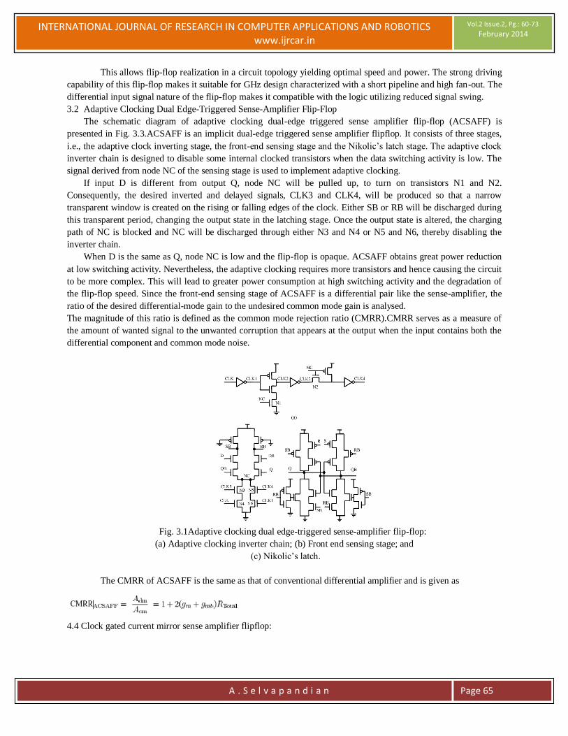
3.2 Adaptive Clocking Dual Edge-Triggered Sense-Amplifier Flip-Flop
The schematic diagram of adaptive clocking dual-edge triggered sense amplifier flip-flop (ACSAFF) is
presented in Fig. 3.3.ACSAFF is an implicit dual-edge triggered sense amplifier flipflop. It consists of three stages,
i.e., the adaptive clock inverting stage, the front-end sensing stage and the Nikolic’s latch stage. The adaptive clock
inverter chain is designed to disable some internal clocked transistors when the data switching activity is low. The
signal derived from node NC of the sensing stage is used to implement adaptive clocking.
If input D is different from output Q, node NC will be pulled up, to turn on transistors N1 and N2.
Consequently, the desired inverted and delayed signals, CLK3 and CLK4, will be produced so that a narrow
transparent window is created on the rising or falling edges of the clock. Either SB or RB will be discharged during
this transparent period, changing the output state in the latching stage. Once the output state is altered, the charging
path of NC is blocked and NC will be discharged through either N3 and N4 or N5 and N6, thereby disabling the
inverter chain.
When D is the same as Q, node NC is low and the flip-flop is opaque. ACSAFF obtains great power reduction
at low switching activity. Nevertheless, the adaptive clocking requires more transistors and hence causing the circuit
to be more complex. This will lead to greater power consumption at high switching activity and the degradation of
the flip-flop speed. Since the front-end sensing stage of ACSAFF is a differential pair like the sense-amplifier, the
ratio of the desired differential-mode gain to the undesired common mode gain is analysed.
The magnitude of this ratio is defined as the common mode rejection ratio (CMRR).CMRR serves as a measure of
the amount of wanted signal to the unwanted corruption that appears at the output when the input contains both the
differential component and common mode noise.
Fig. 3.1Adaptive clocking dual edge-triggered sense-amplifier flip-flop:
(a) Adaptive clocking inverter chain; (b) Front end sensing stage; and
(c) Nikolic’s latch.
The CMRR of ACSAFF is the same as that of conventional differential amplifier and is given as
4.4 Clock gated current mirror sense amplifier flipflop:

INTERNATIONAL JOURNAL OF RESEARCH IN COMPUTER APPLICATIONS AND ROBOTICS www.ijrcar.in
Vol.2 Issue.2, Pg.: 60-73
February 2014
A . S e l v a p a n d i a n
Page 66
4.3Clock gated current mirror sense amplifier
flipflop (a)Pulse generator stage (b)Sensing stage (c)Latching stage
In order to eliminate the redundant transitions in the pulse generator, the CG-SAFF is constructed. It
utilizes the DETSAFF design as a baseline and incorporates the clock gating technique. In CG-SAFF, the clock
gating technique is implemented by embedding a control circuit in the explicit pulse generator so that the PULS
signal generation is disabled in a redundant event. The current mirror sense amplifier has better improvement in the
nose immunity and speed of read circuit. Current Mirror Sense Amplifier takes differential input and amplify them
large signal output. The differential approach presents numerous advantage over single ended counterpart – one of
the most important being common mode rejection. That is such amplifier rejects the noise that is equally injected at
both input. The signal common at both input suppressed at output of amplifier. Clock gated current mirror sense
amplifier having three stages: pulse generator stage, sensing stage, latching stage .In pulse generator stage consist of
4 pmos& 4 nmos, totally 8 transistors. Sensing stage consists of 5 transistors.SB signal was taken in between CM5
& CM3 & RB signal was taken in between CM2 & CM4.latching stage consists of four nmos& four pmos.SB signal
& PULS signal was taken from sensing stage.
4.5 Clock gated full latch sense amplifier flipflop:
4.4Clock gated Full latch sense amplifier flipflop (a)Pulse generator stage (b)Sensing stage (c)Latching
stage
The power problem is one of the most serious limitations in the high performance - VLSI's circuits. The
power dissipation of on chip memories and interface circuits occupies a large portion of the total power dissipation.
Full latch sense amplifier consumes less power than other configuration of sense amplifier. Even though the
conventional latch based on two cross coupled inverters is widely used as a sense amplifier, it always requires some
decoupling at its input. This drawback does not occur for the latch circuit shown in fig -3. The most critical point of
latch-type sense amplifiers is that once the decision process has started, it does not recover unless the circuit is reset
to the metastable Due to fast speed, low power consumption, high input impedance and full-swing output latch type
sense amplifier are very attractive for many applications. . Clock gated current mirror sense amplifier having three
stages: pulse generator stage ,sensing stage, latching stage .In pulse generator stage consist of 4 pmos& 4 nmos
,totally 8 transistors. Sensing stage consists of 9 transistors.SB signal was taken in between CM5 & CM3 & RB

INTERNATIONAL JOURNAL OF RESEARCH IN COMPUTER APPLICATIONS AND ROBOTICS www.ijrcar.in
Vol.2 Issue.2, Pg.: 60-73
February 2014
A . S e l v a p a n d i a n
Page 67
signal was taken in between CM2 & CM4.latching stage consists of four nmos& four pmos.SB signal & PULS
signal was taken from sensing stage.
Comparison Table:
32nm Technology:
Types Set
time (ns)
Hold time(n
s)
Delay(ns)
Power(W)
PDP
DET-SAFF
287 49 336 26.352u 8854.272
DSAFF-Ct mirror
162 42 204 30.040u 6128.16
DSAFF-Full latch
143 52 195 44.495u 8676.525
TABLE 4.1
At 32nm technology dual edge trigger current mirror sense amplifier consumes 30.040uW . Its less than that of dual
edge triggered full latch sense amplifier and also power delay product of dual edge trigger current mirror sense
amplifier is (6128.16) less than that of the dual edge trigger full latch (8676.525).
45nm Technology
Types
Set
time
(ns)
Hold
time(
ns)
Dela
y(ns)
Powe
r(W) PDP
DET-
SAFF 217 32 249
24.8
57u
6189.39
3
DSAF
F-Ct
mirror
102 90 192 26.9
85u 5181.12
DSAF
F-Full
latch
12 45 57 36.9
56u 2106.49
TABLE 4.2
At 45nm technology dual edge trigger current mirror sense amplifier consumes 26.985uW . Its less than that of dual
edge triggered full latch sense amplifier.
65nm Technology:

INTERNATIONAL JOURNAL OF RESEARCH IN COMPUTER APPLICATIONS AND ROBOTICS www.ijrcar.in
Vol.2 Issue.2, Pg.: 60-73
February 2014
A . S e l v a p a n d i a n
Page 68
TABLE 4.3
90nm Technology:
TABLE 4.4
At 65nm technology dual edge trigger current mirror sense amplifier consumes 0.323mW. Its less than that of dual
edge triggered full latch sense amplifier and also power delay product of dual edge trigger current mirror sense
amplifier is (23.256)less than that of the dual edge trigger full latch (70.378).
At 90nm technology dual edge trigger current mirror sense amplifier consumes2.227mW. Its less than that of dual
edge triggered full latch sense amplifier and also power delay product of dual edge trigger current mirror sense
amplifier is (204.884) less than that of the dual edge trigger full latch (419.796).
MICROWIND
MICROWIND is truly integrated EDA software encompassing IC designs from concept to completion,
enabling chip designers to design beyond their imagination. MICROWIND integrates traditionally separated front-
end and back-end chip design into an integrated flow, accelerating the design cycle and reduced design
Types
Set
time
(ns)
Hold
time
(ns)
Delay
(ns)
Power
(W) PDP
DET-
SAFF 65 31 96 1.494m
143.4
24
DSAFF-Ct
mirror
26 66 92 2.227m 204.8
84
DSAF
F-Full
latch
128 10 138 3.042m 419.7
96
Types
Set
time
(ns)
Hold
time
(ns)
Dela
y(ns)
Power
(W) PDP
DSAF
F-Ct
mirror
16 56 72 0.323m 23.256
DSAF
F-Full
latch
112 42 154 0.457m 70.378
DET-
SAFF 137 35 172 0.239m 41.108

INTERNATIONAL JOURNAL OF RESEARCH IN COMPUTER APPLICATIONS AND ROBOTICS www.ijrcar.in
Vol.2 Issue.2, Pg.: 60-73
February 2014
A . S e l v a p a n d i a n
Page 69
Complexities. It tightly integrates mixed-signal implementation with digital implementation, circuit simulation,
transistor-level extraction and verification – providing an innovative education initiative to help individuals to
develop the skills needed for design positions in virtually every domain of IC industry
The present manual introduces the design and simulation of CMOS integrated circuits, in an attractive way
thanks to user-friendly PC tools Dsch and Microwind 3.1. The DSCH program is a logic editor and simulator.
DSCH is used to validate the architecture of the logic circuit before the microelectronics design is started. DSCH
provides a user friendly environment for hierarchical logic design, and simulation with delay analysis, which allows
the design and validation of complex logic structures. A key innovative feature is the possibility to estimate the
power consumption of the circuit. Some techniques for low power design are described in the manual.
The MICROWIND 3.1 program allows the student to design and simulate an integrated circuit at physical
description level. The package contains a library of common logic and analog ICs to view and simulate.
MICROWIND 3.1 includes all the commands for a mask editor as well as original tools never gathered before in a
single module (2D and 3D process view, VERILOG compiler, tutorial on MOS devices). We can gain access to
Circuit Simulation by pressing one single key. The electric extraction of your circuit is automatically performed and
the analog simulator produces voltage and current curves immediately.
Simulation and output wave form
5.1DET-SAFF schematic diagram:
Simulation and output wave form
5.1DET-SAFF schematic diagram:

INTERNATIONAL JOURNAL OF RESEARCH IN COMPUTER APPLICATIONS AND ROBOTICS www.ijrcar.in
Vol.2 Issue.2, Pg.: 60-73
February 2014
A . S e l v a p a n d i a n
Page 70
5.2DET-SAFF output diagram:
5DET-current mirror schematic diagram

INTERNATIONAL JOURNAL OF RESEARCH IN COMPUTER APPLICATIONS AND ROBOTICS www.ijrcar.in
Vol.2 Issue.2, Pg.: 60-73
February 2014
A . S e l v a p a n d i a n
Page 71
6DET-current mirror outputdiagram
5.7DET-full latch schematic diagram:
5.8DET-full latch output diagram

INTERNATIONAL JOURNAL OF RESEARCH IN COMPUTER APPLICATIONS AND ROBOTICS www.ijrcar.in
Vol.2 Issue.2, Pg.: 60-73
February 2014
A . S e l v a p a n d i a n
Page 72
CONCLUSION
This project presents four types of dual edge triggered sense amplifier flipflop by using current mirror sense
amplifier circuit and full latch sense amplifier circuit such as double edge triggered sense amplifier flip flop using
current mirror , double edge triggered sense amplifier flip flop using full latch and clock gated sense amplifier flip
flop using current mirror, clock gated sense amplifier flipflop using full latch. According to the power and PDP
analysis the dual edge trigger current mirror sense amplifier is superior to dual edge triggered full latch sense
amplifier. At 45nm technology the dual edge trigger current mirror sense amplifier consumes 26.985uW. At 45nm
technology the clock gated current mirror sense amplifier consumes 3.788uW.
It is concluded that the dual edge trigger current mirror sense amplifier flipflop is suitable to design the VLSI
clocking system with high switching activity and the clock gated current mirror sense amplifier flipflop is suitable to
design the VLSI clocking system with low switching activity.
REFERENCES
1.Myint WaiPhyu, Member, IEEE, Kangkang Fu, Wang Ling Goh, Senior Member, IEEE, andKiat-Seng Yeo,
Senior Member, IEEE“Power-Efficient Explicit-Pulsed Dual-Edge TriggeredSense-Amplifier Flip-Flops”
(2011)IEEE Trans. VeryLarge Scale Integr (VLSI) Syst, VOL. 19, no. 1,pp.,1-9
2. Kawaguchi.H and T. Sakurai, (1998)“A reduced clock-swing flip-flop (RCSFF) for 63% power reduction,” IEEE
J. Solid-State Circuits, vol. 33, no. 5, pp. 807–811.
3. Kim.C.L. and S. Kang, (2002), “A low-swing clock double edge-triggered flip-flop” in IEEE J. Solid-State
Circuits, vol. 37, no. 5, pp. 648–652.
4. Klass.F, C. Amir, A. Das, K. Aingaran, C. Truong, R.Wang, A. Mehta, R. Heald, and G. Yee,(1998) “Semi-
dynamic and dynamic flip-flops with embedded logic,” in Symp. VLSI Circuits, Dig. Tech. Papers, pp. 108–109.
5. Kong .B., S. Kim, and Y. Jun, “Conditional-capture flip-flop for statistical power reduction,(2001), ” IEEE J.
Solid-State Circuits, vol. 36, no. 8, pp. 1263–1271.
6. Markovic. D., B.Nikolic, and R. Brodersen, (2001), “Analysis and design of low-energy flip-flops,” in
Processing of International Symposium Low Power Electronic Design, Huntington Beach, CA, pp. 52–55.
7. Nikolic .B, V. G. Oklobzija, V. Stojanovic, W. Jia, J. K. Chiu, and M. M. Leung, (2000)“Improved sense-
amplifier-based flip-flop: Design and measurements”.
8. Partovi.H, R. Burd, U. Salim, F.Weber, L. DiGregorio, and D. Draper, (1996)“Flow-through latch and edge-
triggered flip-flop hybrid elements,” in ISSCC Dig., pp. 138–139.
9. Peiyi Zhao, Jason McNeely, WeidongKuang, Nan Wang, and Zhongfeng Wang,(2009), “Design of Sequential
Elements for Low PowerClocking System”, inIEEE Transactions on Very Large Scale Integration (VLSI) Systems
10. Sakurai.T, “Low –power CMOS design through Vth control and low swing circuits,” (1997)inProc. ISLPED,
pp. 1–6.

INTERNATIONAL JOURNAL OF RESEARCH IN COMPUTER APPLICATIONS AND ROBOTICS www.ijrcar.in
Vol.2 Issue.2, Pg.: 60-73
February 2014
A . S e l v a p a n d i a n
Page 73
11. Teh. C.K., M. Hamada, T. Fujita, H. Hara, N. Ikumi, and Y. Oowaki, (2006) “Conditional Data Mapping Flip-
Flops for Low-Power and High-performance systems,” IEEE Transactions Very Large Scale Integr. (VLSI) Syst.,
vol. 14, no.12, pp. 1379–1383.
12.Vijendra K Maurya, Sanjay Jaiswal, KumkumVerma, AnkitSanadhya “Design and Implementation of High
Speed Sense Amplifier”IEEE Trans. Very Large ScaleIntegr. (VLSI) Syst.,
13. Zhao.P, J. McNeely, P. Golconda, M. A. Bayoumi, W. D. Kuang, and B. Barcenas,(2007) “Low power clock
branch sharing double-edge triggered flip-flop,” IEEE Trans. Very Large Scale Integr. (VLSI) Syst., vol. 15, no. 3,
pp. 338–345.
14. Zhao.P, J. McNeely, S.Venigalla, G. P.Kumar,M. Bayoumi, N.Wang, and L. Downey, “Clocked-pseudo-NMOS
flip-flops for level conversion in dual supply systems,” IEEE Trans. Very Large Scale Integr.(VLSI) Systems.IEEE
J. Solid-State Circuits, vol. 35, no. 6, pp. 876–883.
15. Zhao.P, T. Darwish, and M. Bayoumi, “High-performance and low power conditional discharge flip-
flop,”(2004) IEEE Trans. Very Large ScaleIntegr. (VLSI) Syst., vol. 12, no. 5, pp. 477–484.