Design and Analysis of Planar Dual Mode Antenna … and Analysis of Planar Dual Mode Antenna Array...
56
Design and Analysis of Planar Dual Mode Antenna Array MSEE Project Report By Vikram Arora Signature Date Project Advisor: _____________ _______ Professor Ray Kwok Project Co-Advisor: _____________ _______ Professor Masoud Mostafavi Graduate Coordinator: _____________ _______ Professor Peter Reischl Department of Electrical Engineering San Jose State University San Jose, CA 95192-0084 _____________________________________________________________ Vikram Arora 004023644 1901 Halford Ave, Apt 149, Santa Clara, CA 95051 408-615-1473 [email protected]
-
Upload
nguyenthuan -
Category
Documents
-
view
233 -
download
5
Transcript of Design and Analysis of Planar Dual Mode Antenna … and Analysis of Planar Dual Mode Antenna Array...

Design and Analysis of Planar Dual Mode Antenna
Array
MSEE Project Report
By
Vikram Arora
Signature Date
Project Advisor: _____________ _______
Professor Ray Kwok
Project Co-Advisor: _____________ _______
Professor Masoud Mostafavi
Graduate Coordinator: _____________ _______
Professor Peter Reischl
Department of Electrical Engineering
San Jose State University
San Jose, CA 95192-0084
_____________________________________________________________ Vikram Arora
004023644
1901 Halford Ave, Apt 149, Santa Clara,
CA 95051
408-615-1473

ii
Abstract
Planar microstrip patch antennas are the preferred choice of antennas for printed circuit
boards due to their low profile, mechanical ruggedness, easy mounting and low cost.
There are two categories of simulation software available for analysis of patch antennas,
Full Wave Models based and Analytical Models based. Full Wave Models based
software take the rigorous approach, and produce good accuracy, but cost thousands of
dollars, have significant learning curves and parametric analysis can take hours.
Analytical Models based approach makes one or more significant approximations to
simplify the problem. The results have lesser accuracy especially with thick substrates,
but parametric variations can be solved very quickly, which helps with gaining insight
into underlying physics. Special purpose user interface for specific application can be
developed leading to very small learning curve for user, and development cost is
significantly lower. Not many commercial analytical models based softwares with
friendly user interface are available, and command line interface has only limited
usefulness. In this project Matlab Graphical User Interface based patch antenna
simulation software with array simulation capability has been developed. The software
has the capability to predict return loss, circular polarization, radiation pattern based upon
cavity model and allow simulation of antenna array. A dual band antenna has been
fabricated and the results have been compared with simulation results. The measurement
results show good agreement with simulation results within the tolerance of fabrication
and experiment method.

iii
Acknowledgements
I owe my thanks to my advisors:
Prof. Ray Kwok: Thanks for your constant support, encouragement, guidance,
sharing your wisdom, and always being there to help out.
Prof. Masoud Mostafavi: Thanks for your enthusiasm for project, feedback and
advice.
I would like to thank Irma Alarcon for her help and support in E347 lab.
I owe a special gratitude to my wife, Ritu, and my newborn, Megha, thanks for
being my motivation. Finally a special thanks to my family in India – my parents
and my sister, Meena, thanks for your constant encouragement.

iv
Table of Contents
1. Introduction…………………………………………………………………..1
1.1 Characteristics of Microstrip Patch Antennas……………..……..………..1
1.2 Methods of Feeding………………………………………………………..3
1.3 Principle of Operation……………………………………………………...3
2. Modeling of Microstrip Patch Antenna……………………………………..5
2.1 Full Wave Models………………………………………………………….5
2.2 Analytical Models………………………………………………………….6
2.3 Comparison between Full Wave Models and Analytical Models …………6
2.4 Comparison between Transmission Line Model and Cavity Model……….7
3. Cavity Model for Microstrip Patch Antenna………………………………..9
3.1 Electric Wall Boundary Condition………………………………………….9
3.2 Magnetic Wall boundary Condition……………………………………….10
3.3 Input Impedance…………………………………………………………..10
3.3.1 Incorporating Losses………………………………………………13
3.3.2 Accounting for fringing of fields………………………………….15
3.4 Circular Polarization………………………………………………………16
3.4.1 Circular Polarization with Singly Fed Patch………………………16
4. Radiation Pattern…………………………………………………………….18
4.1 Radiated Fields for TM01 mode…………………………………………..19
4.2 Antenna Array……………………………………………………………..21
4.2.1 Array Factor for Planar Array……………………………………..22
5. Matlab Implementation………………………………………………………23

v
5.1 Cavity Model Based Simulation Software………………………………….23
5.2 2D Radiation Pattern and Array Pattern…………………………………….26
6. Fabrication and Measurements………………………………………………30
6.1 Measurements………………………………………………………………34
6.2 Comparison of Simulation with Measurement Results for Single Band
Antenna……………………………………………………………………..36
6.2.1 Analysis of Return Loss Measurement Results…………………….36
6.2.2 Comparison of Radiation Pattern Results…………………………..38
6.3 Comparison of Simulation with Measurement Results for Dual Band
Antenna ………………………………………………………………………....39
7. Conclusions…………………………………………………………………….43
8. Future Work……………………………………………………………………44
References………………………………………………………………………….45
Appendices
A1: Return Loss Measurements for 2.4 GHz single band antenna……………..47
A2: Return Loss Measurements for 2.4 GHz band of dual band antenna…… 52
A3: Return Loss Measurements for 5.8 GHz band of dual band antenna…….57
B1: Radiation Pattern Measurements for 2.4 GHz single band antenna………62
B2: Radiation Pattern Measurements for 2.4 GHz band of dual band
antenna…………………………………………………………………………………65
B3: Radiation Pattern Measurements for 5.8 GHz band of dual band
antenna…………………………………………………………………………………67
C1: Matlab code for cavity model based simulator……………………………..69

vi
C2: Matlab code for 2D Radiation Pattern simulator…………………………..99
C3: Matlab code for 3D Radiation Pattern simulator…………………………..117

vii
List of Figures
Figure 1.1: Microstrip Patch Antenna
Figure 3.1: Circular Polarization with Singly Fed Patch
Fig 4.1 Microstrip Patch Antenna Radiating slots
Figure 4.2 Planar Array
Figure 5.1 Cavity based Simulator Graphical User Interface
Figure 5.2 2D Radiation Pattern
Figure 5.3 3D Radiation Pattern
Figure 6.1: 2.4 GHz circularly polarized test antenna
Figure 6.2: 2.4, 5.8 GHz dual band circularly polarized test antenna
Figure 6.3 Simulation of 2.4 GHz band
Figure 6.4 Simulation of 5.8 GHz band
Figure 6.5: Measurements with Network analyzer in E347 lab
Figure 6.6: Return Loss Measurement with network analyzer in E347 lab
Figure 6.7: Measurement for circular polarization
Figure 6.8: Return Loss Comparison for 2.4 GHz single band antenna
Figure 6.9: Return Loss Comparison for 2.4 GHz single band antenna with
probe location 3mm off from optimized value
Figure 6.10: Radiation Pattern Comparison for 2.4 GHz single band antenna
Figure 6.11: Measured Axial Ratio for 2.4 GHz single band antenna
Figure 6.12: Return Loss Comparison for 2.4 GHz band of dual band
antenna with probe location 3mm off from optimized value
Figure 6.13: Radiation Pattern Comparison for 2.4 GHz band of dual band

viii
Antenna
Figure 6.14: Measured Axial Ratio for 2.4 GHz single band antenna
Figure 6.15: Return Loss Comparison for 5.8 GHz band of dual band
antenna with probe location 3mm off from optimized value
Figure 6.16: Radiation Pattern Comparison for 5.8 GHz band of dual band
Antenna
Figure 6.17: Measured Axial Ratio for 5.8 GHz single band antenna

ix
List of Tables
Table A1.1: Return Loss (|S11|) measurement for 2.4 GHz single band antenna
Table A2.1: Return Loss (|S11|) measurement for 2.4 GHz band of dual band
Table A3.1: Return Loss (|S11|) measurement for 5.8 GHz band of dual band
Table B1.1: Radiation Pattern measurement for 2.4 GHz single band antenna –
Rotation around Z axis
Table B1.2: Radiation Pattern measurement for 2.4 GHz single band antenna –
Rotation around Y axis
Table B1.3: Radiation Pattern measurement for 2.4 GHz single band antenna –
Antenna rotate 900 around X axis, Rotation around Y axis
Table B1.4: Radiation Pattern measurement for 2.4 GHz single band antenna –
Axial Ratio, Rotation around Z axis
Table B2.1: Radiation Pattern measurement for 2.4 GHz band of dual band antenna
– Rotation around Z axis
Table B2.2: Radiation Pattern measurement for 2.4 GHz band of dual band antenna
– Rotation around Y axis
Table B2.3: Radiation Pattern measurement for 2.4 GHz band of dual band antenna
– Antenna rotate 900 around X axis, Rotation around Y axis
Table B2.4: Radiation Pattern measurement for 2.4 GHz band of dual band antenna
– Axial Ratio, Rotation around Z axis
Table B3.1: Radiation Pattern measurement for 5.8 GHz band of dual band antenna
– Rotation around Z axis
Table B3.2: Radiation Pattern measurement for 5.8 GHz band of dual band antenna

x
– Rotation around Y axis
Table B3.3: Radiation Pattern measurement for 5.8 GHz band of dual band antenna
– Antenna rotate 900 around X axis, Rotation around Y axis
Table B3.4: Radiation Pattern measurement for 5.8 GHz band of dual band antenna
– Axial Ratio, Rotation around Z axis

1
1. Introduction
The tremendous growth in the wireless communication in the commercial systems has
produced the need for antennas, which are low in cost and easier to fabricate and
integrate with other microwave components. Planar microstrip patch antennas are the
preferred choice of antennas for printed circuit boards due to their low profile,
mechanical ruggedness, easy mounting, low cost and ease of integration with other
microwave devices in microstrip technology. Both linear and circular polarizations are
possible. Numerous advancements have occurred in the microstrip antenna technology in
past few decades that has enabled their widespread use in personal communication
systems, mobile satellite communications and wireless local area networks (WLANs)
[14].
Microstrip antennas have some limitations also. They are inherently narrow band,
have low gain, and polarization purity is typically low. [3]. Some of these limitations can
be overcome with specific techniques e.g bandwidth can be increased by increasing the
substrate height.
1.1 Characteristics of Microstrip Patch Antennas
Microstrip antennas consist of a patch of metallization over ground plane separated by a
dielectric substrate. They are commonly referred to as patch antennas also. The thickness
of substrate, h is usually very small compared to λ0, the free space wavelength, the typical
range being, 0.003λ0 ≤ h ≤ 0.05λ0 [5]. Patch antennas are normally broadside antennas,
although it is possible to design end fire radiation also. The length of patch is typically
order of λ0/2 i.e L ≈ λ0/2. Numerous shapes of patch geometry has been studied and used

2
Figure 1.1: Microstrip Patch Antenna
in patch antennas over past few decades e.g rectangular, circular, elliptical and triangular
[3]. Rectangular and circular seems to be the most often used geometries for patch. The
rectangular geometry has been investigated in this project.
A large number of substrates can be used for microstrip patch antennas. The
dielectric constant is typically in the range, 2.2 ≤ εr ≤ 12 [5]. The substrates with low
dielectric constant produce better radiation efficiency due to loosely bound fields, but end
up larger size of patch. On the other hand, substrates with higher dielectric constants lead

3
of small patch sizes, but are less efficient radiators due to tightly bound fields. A
compromise needs to be reached owing to other considerations e.g integration with other
microwave components.
Both linear and circular polarizations can be achieved with microstrip patch
antennas. Array of patch antennas can be used in order to increase the directivity or to
have scanning capabilities.
1.2 Methods of Feeding
The two most common methods of feeding microstrip patch antennas are microstrip line
and coaxial probe. A number of other methods have been developed also e.g proximity-
coupled microstrip feed, aperture coupled microstrip feed and coplanar waveguide feed
[3]. The major requirement from the feed is the efficient transfer of power from feed to
antenna. Typically the impedance matching criteria along with other considerations like
feeding of array arrangements dictate the selection and design of feed. The coaxial feed
has been used in this project. N type coaxial connector is typically used, in which the
connector is attached to the back side (ground plane) of antenna and coaxial center
conductor is passed through the substrate and soldered to the patch element.
1.3 Principle of Operation
The basic mechanism of radiation of patch antenna is the fringing of fields beyond the
edges of patch element, as shown in Figure 1.1. The feeding of patch antenna produces
the current density and electric and magnetic fields in the region between patch element
and ground plane, the fields fringe beyond the physical dimensions of patch, and these

4
fringe fields produce the radiation. The amount of fringing of fields depends upon the
dimensions of patch, and the height and dielectric constant of substrate. The increase in
height of substrate causes increase in fringe fields. The higher dielectric constant of the
substrate binds the fields more tightly inside the substrate region between patch and
ground plane and reduces the fringe fields. More the amount of fringing, better would be
the radiation efficiency of patch antenna.

5
2. Modeling of Microstrip Patch Antenna
A large number of methods have been developed to model the microstrip patch antenna.
A good model of antenna should be able to predict the desired electrical characteristics of
antenna with accurate enough results for the given purpose, and should be able to do that
in computationally efficient way. Other desirable characteristics of the model are
reasonably fast solutions for parametric variations of design parameters and user-friendly
interface. Most of the models developed so far for patch antennas can be divided into two
categories a) Full Wave Models b) Analytical Models [14].
2.1 Full Wave Models
The full wave models for microstrip patch antennas take the rigorous approach and
accurately models the dielectric substrate. They produce very accurate solutions, however
computational cost is typically quite high. The solutions for parametric variations can
take hours of simulation time. There are three types of approaches used for full wave
models a) Method of Moments (MoM) b) Finite Difference Time Domain (FDTD) c)
Finite Element Method (FEM). The MoM approach assumes the substrate to be infinite
and model it with exact Greens functions. The patch and ground plane conductors are
modeled with basis functions. FDTD and FEM are brute force kind of methods, the entire
structure is subdivided and modeled with basis functions. These two methods have the
capability to handle any shape of the structure, however they are computationally very
expensive. A large number of commercial software based upon full wave models have
become available in market, a partial list can be found in chapter 1 of [14].

6
2.2 Analytical Models
The analytical models for microstrip antenna make one or more significant
approximations to greatly simplify the problem. This typically allows the derivation of
closed form equations with the result that solutions can be computed with much lesser
computation expense as compared to full wave models. However this also implies that
the computed solutions are less accurate. There are two main types of analytical models
developed for patch antennas a) Transmission Line Model and b) Cavity Model. The few
variants and generalizations of these approaches have also been developed [3].
The transmission line based approach models the region between patch and
ground plane as a section of transmission line of length, L. The dimensions of patch and
substrate parameters determine the characteristic impedance and propagation constant of
transmission line.
The cavity model based approach models the region between patch and ground
plane as cavity with electric walls on top and bottom, and magnetic walls along the
periphery. The dimensions of patch and substrate parameters determine the modes of the
cavity.
2.3 Comparison between Full Wave Models and Analytical Models
The full wave models based software for antenna analysis produce very accurate results,
and are capable of predicting all characteristics of antenna e.g resonance frequency,
return loss as function of frequency sweep, radiation pattern and cross polarizations.
However they are computationally very expensive, and cost thousands of dollars. They
are typically general purpose Electromagnetic Analysis software and there is a significant

7
learning curve to use the interface for given antenna design. On the other hand, analytical
model based software can solve parametric variations quickly, which helps in gaining the
physical insight into the underlying physics of the problem. The results are less accurate,
however accuracy might be sufficient for the given application. Specific user interface
can be developed which would mean a very short or negligible learning curve. A few
such software are available, but number of them are command line based, which has
limited usefulness [8]. In this project, we propose to write a Matlab GUI based software
for analytical modeling of patch antenna. The software is to have the following abilities
a) Ability to simulate return loss v/s frequency sweep
b) Ability to predict circular polarization (CP)
c) Ability to simulate dual band antenna
d) Ability to simulate radiation pattern
e) Ability to simulate antenna array
2.4 Comparison between Transmission Line Model and Cavity Model
The transmission line model is simple but it produces acceptable results only when the
feed point is near the radiating edges [2]. A fundamental drawback of this model is that it
does not account for non-resonant modes while predicting the input impedance of the
antenna.
The cavity model on the other hand, is based upon the modal expansion technique
and it incorporates the affect of non-resonant modes on the input impedance. The results
computed using the cavity model has closer agreement with experimental results even
when the feed point is away from the edges of the patch. It is also possible to predict

8
circular polarization using the cavity model. The mathematical formulation of cavity
model is little bit more complex that transmission line model, but it is possible to derive
the closed form expressions, with the result that computational efficiency is not sacrificed
much.
In this project we propose to use the cavity model for the patch antenna in Matlab
GUI based software.

9
3. Cavity Model for Microstrip Patch Antenna
The cavity model for analyzing the patch antenna was proposed by Richards, Lo
and others [6]. Further improvements have been proposed since then [7][9][10]. The
region of substrate between patch and ground plane, termed as interior region, is modeled
a cavity, bounded by electric walls on top and bottom and magnetic walls along the
periphery. The substrate is assumed to be thin i.e h << λ0. The fields in the interior region
are assumed not to vary along z direction i.e ∂/∂z = 0, see Figure 1.1 for coordinate
system definition.
3.1 Electric Wall Boundary Condition
The patch and ground plane are assumed to be perfect conductors, and assumed to
represent electric wall. The boundary conditions for electric wall are [6]
(3.1d) ˆ
(3.1c) 0ˆ
(3.1b) 0ˆ
(3.1a) ˆ
s
s
JHn
En
Bn
Dn
rr
r
r
r
=×
=×
=•
=• ρ
The electric wall assumption implies that the tangential component of E field is
zero, and it has only normal component i.e Ez in our case. Additionally normal
component of magnetic field is zero, and it has only tangential components i.e Hx and Hy
in our case.

10
3.2 Magnetic Wall boundary Condition
The interior region between patch and ground plane is assumed to be bounded by
magnetic wall along the periphery. The boundary conditions for magnetic wall are [6]
(3.2d) 0ˆ
(3.2c) ˆ
(3.2b) 0ˆ
(3.2a) 0ˆ
=×
−=×
=•
=•
Hn
MEn
Bn
Dn
sr
rr
r
r
The magnetic wall assumption implies E field normal to the periphery and H field
tangential to the periphery are zero.
The above boundary condition assumptions lead to the assumption that only non-
zero field components are Ez, Hx and Hy.
3.3 Input Impedance
The input impedance for a given feed location is computed by first computing the E field
based upon the modes of cavity and then artificially introducing the radiation as a loss
component along with dielectric and conductor loss [3].
With only Ez, Hx and Hy as non zero field components, the wave equation
becomes
r
z
k
JjEky
E
x
E zz
εεµω
ωµ
0022
02
2
2
2
2
)3.3(
=
=+∂
∂+
∂
∂
11
J is the feed current. The feed is assumed to be coaxial in this project.
The electric field is then expressed in terms of various modes of cavity
where Amn are amplitude coefficients of orthonormalized eigenfunctions ψmn. The
eigenfunction ψmn must satify the wave equation and following boundary conditions and
normalization conditions
Solving equations 3a to 3d gives
The next step is to determine Amn. Feed current determines them, so we need to model
the feed. Substituting equation 3.6 into 3.4, multiplying both sides of 3.4 with ψ*mn ,
integrating over the area of patch, and making use of 3.5a to 3.5d, we obtain [3]
)4.3(),(),( ∑∑=m n
mnmnz yxAyxE ψ
)5.3(1
)5.3(0)(
)5.3(00
)5.3(00
*
2
2
2
2
2
ddxdy
ckxx
bWyandyaty
aLxandxatx
x y
mnmn
mnmn
mn
mn
=
=+∂
∂+
∂
∂
===∂
∂
===∂
∂
∫ ∫ ψψ
ψ
ψ
ψ
222,/,/
0,2
0,1
)6.3(...,2,1,0,)cos()cos(),(
nmmnnm
p
p
nm
mm
mn
kkkWnkLmk
pif
pif
pnmykxkLW
yx
+===
≠=
==
==
ππ
ε
ε
εεψ

12
The feed model used in this project is the uniform current density over rectangular cross
section, DxDy with area of rectangular cross section equal to actual cross sectional area of
probe [3].
Using 3.8 in 3.7 gives
Inserting 3.6 and 3.9 in 3.4 gives
)7.3(*
22
0 dxdyJkk
jA z
feed
mn
mn
mn ∫∫−= ψ
ωµ
elsewhereJ
DyyDyandDxxDxDyDIJ
z
yyxxxz
,0
(3.8) 2/2/2/2/,/ 00000
=
+≤≤−+≤≤−=
(3.10) ))2/((sin))2/((sin where,
(3.9) )cos()cos(
1
0022
0
*
022
0
WDncLDncG
GykxkLWkk
j
dxdyIkk
j
DDA
yxmn
mnnmnm
mn
feed
mn
mnyx
mn
ππ
εεωµ
ψωµ
=
−=
−= ∫∫
(3.11) ),(),(
),(0 0
22
0000 ∑∑
∞
=
∞
= −=
m n
mn
mn
mnmn
z Gkk
yxyxIjyxE
ψψωµ

13
Based upon the E field computed above input impedance can be computed as follows
3.3.1 Incorporating Losses
If we do not include the losses in equation 3.14, input impedance would be purely
reactive as all the quantities under the summation sign are real. The dielectric losses as
well as radiation losses need to be incorporated in order to correctly predict the input
impedance. The typical method to incorporate losses is to replace ε0εr by ε0εr(1 – j tan δ),
where tan δ is the loss tangent of the substrate. The radiation loss can accounted for by
artificially increasing the loss tangent term [2].
r
m n
mn
mn
in
zin
inin
k
Gkk
yxhjZ
hyxEV
I
VZ
mn
εεµω
ψωµ
0022
0 022
00
2
0
00
0
where
(3.14) ),(
(3.13) ),(
(3.12)
=
−−=
−=
=
∑∑∞
=
∞
=
patchunder storedenergy totalaveraged Time: power, Radiated :
'
"tandepth,skin : tangent,loss substrate :
(3.15) tan
Tr
T
r
eff
WP
W
P
h
ε
εδδ
ωδδ
≈∆
+∆
+=

14
Accounting for losses in 3.4 yields
The radiated power, Pr can be computed by integrating the far fields as in [8], however
[8] also describes approximating the sin and cos terms in far field expressions with
polynomial, doing the analytical integration and coming up with following for Pr
The stored electric energy, at resonance for dominant mode, is given by [8]
The equations 3.17 and 3.18 can be used in 3.15 to compute δeff, which then can be used
to compute input impedance from 3.16.
(3.16) )1(
),(
0 022
00
2
00
∑∑∞
=
∞
= −−−=
m n
mn
mneffr
in Gkjk
yxhjZ mn
δε
ψωµ
2
0
2
0
22242
0
2 and
where
17.3)1897
2(5
)42015
1)(1(23040
=
=
+−++−−=
λ
λ
π
π
WB
LA
AABAAB
AVPr
(3.18) 8
2
0 0
h
LWVW
r
T
εε=

15
3.3.2 Accounting for fringing of fields
It was mentioned in chapter 1 that fields in the region between the patch and ground
plane extend beyond the physical dimensions of the patch. This phenomenon is called
fringing of fields and is actually responsible for the radiation from patch antenna. The
fringing of fields makes the patch look electrically larger than its physical dimensions.
The affect of fringing of fields has originally been accounted for in transmission line
model [5] , but has been proposed to use in cavity model also [9].
Since a portion of fields exist in the substrate and a portion in the air, the concept
of effective dielectric constant, εreff is introduced [5]. The effective dielectric constant is
given by
The effective dielectric constant is then used to find the extension of length, ∆L on each
side and effective length, Leff [5][9]
The effective length, Leff is used in place of L to compute input impedance.
(3.19) 1212
1
2
12/1−
+
−+
+=
W
hrr
reff
εεε
(3.21) 2
(3.20)
)8.0)(258.0(
)264.0)(3.0(
412.0
LLL
h
Wh
W
h
L
eff
reff
reff
∆+=
+−
++=
∆
ε
ε

16
3.4 Circular Polarization
One of the requirements mentioned for the proposed software is to be able to predict and
design for circular polarization. Circular polarization is achieved in rectangular patch
antennas by exciting two orthogonal modes, which are, equal in amplitude but differ by
90o in phase difference. There are two fundamentally different methds of achieving this.
The first method involves exciting two orthogonal modes with a single feed and
perturbing the dimensions or interior of patch in such a way that the magnitudes of two
modes are essentially equal, but they have 90o phase difference. This is often referred to
as singly-fed patch. The second method involves directly feeding two orthogonal modes
with a device that provides equal amplitude and 90o phase difference [13]. The second
method involves extra microwave circuitry and is hence expensive. We propose to use
the first method in this project.
3.4.1 Circular Polarization with Singly Fed Patch
There are multiple ways of obtaining circular polarization with singly fed patch
antenna also. One method is to remove a pair of corners and adjust the dimensions of cut
outs to excite orthogonal modes with equal magnitude but 90o phase difference. In
another method, the design starts with a square patch, then the dimensions of square
patch are perturbed and patch is fed at a point on or close to the one of the diagonal, such
that two degenerate modes TM01 and TM10 are excited with equal magnitude but 90o
phase difference at desired frequency [13] as shown in Fig 3.1. The second method has
been used in this project.

17
Figure 3.1: Circular Polarization with Singly Fed Patch
The cavity model can be used to approximate the ratio of orthogonal components of E
field in far field region [2][13]
The ratio needs to be +j or –j for circular polarization
(3.22) )2
(sin)/cos()(
)/cos()(
0
22
0
22
L
Dc
WykkL
LxkkW
E
E x
y
x
mn
mnπ
π
π
−
−=
)24.3(
(3.23)
LHCPforjE
E
RHCPforjE
E
y
x
y
x
−=
=

18
4. Radiation Pattern
The radiated fields from a patch antenna for a given model, can be computed by
assuming the four side-walls as the four narrow apertures or slots [5] as shown in Fig 4.1.
The fields radiated by slots separated by length add along the principal E plane, which is
the XY plane and principal H plane, which is the YZ plane in Fig 4.1, while the fields
radiated by slots separated by width cancel each other. The slots are represented by
equivalent electric current density Js and magnetic current density, M s.
Fig 4.1 Microstrip Patch Antenna Radiating slots

19
If the electric and magnetic fields at the slot are Ea and Ha, current densities are
given by
(4.2) ˆ
(4.1) ˆ
as
as
EnM
HnJ
rr
rr
×−=
×=
The cavity model assumes the perfect magnetic wall along the periphery of the
region between the patch and ground plane, so the tangential components of magnetic
field along the slots are assumed to be zero, and hence electric current density, Js is taken
as zero. So the radiated fields are computed based upon the magnetic current density, Ms.
The ground plane can be accounted for by using the image theory, which will double the
magnetic current density given by equation 4.2 i.e
(4.3) ˆ2 as EnMrr
×−=
Using the equivalence principle [5], each of the two radiating slots, radiates the
same fields as a magnetic dipole with magnetic current density given by 4.3. The radiated
fields are computed for one slot and then total fields are computed by multiplying with an
array factor corresponding to two slots.
4.1 Radiated Fields for TM01 mode
The radiated field from a slot of patch antenna is computed using the equivalent magnetic
current density given by equation 4.3. By treating the slot as an aperture, the radiated
fields are computed as [5]

20
(4.7) cos2
(4.6) cossin2
where
(4.5) )sin()sin(
sin2
(4.4) 0
0
0
000
θ
φθ
θπ
φ
θ
WkZ
hkX
Z
Z
X
X
r
ehWEkjE
EE
rjk
r
=
=
+=
≈≈−
The array factor for two elements of same magnitude and phase, separated by a
distance Leff along y axis is given by
(4.8) sinsin2
cos20
= φθeffLk
AF
Multiplying 4.5 and 4.8, and assuming k0h << 1, and putting V0 = hE0, where V0
is voltage across the slot, gives
(4.9) sinsin2
coscos
)cos2
sin(
sin2 0
0
00
+=−
φθθ
θθ
πφ
effrjk Lk
Wk
r
eVjE
The equation 4.9 is used in this project to compute and plot the radiation pattern
for patch antenna.

21
4.2 Antenna Array
The radiation pattern from a single patch antenna or any typical antenna
element for that matter is typically very wide. The arrays of antennas are typically
used to obtain the desired directivity. The arrays are used for beam scanning
applications also, where the maxima of beam is pointed in different directions by
adjusting the relative phase differences between elements of array.
The most common arrangement of elements is a linear array, with uniform
amplitude and constant progressive phase difference between elements. A number
of such linear arrays can be placed besides each other to form a planar array. In
this project, we use the planar array, with uniform amplitude and constant
progressive phase difference between elements as shown in Figure 4.2.
Figure 4.2 Planar Array

22
4.2.1 Array Factor for Planar Array
Consider a linear array of M elements placed along x axis, separated from
previous element by distance, dx, with uniform amplitude I0 and constant progressive
phase different βx. The array factor for such an arrangements is given by
(4.10) 1
)cossin)(1(
0∑=
+−=M
m
kdmj xxeIAFβφθ
Now consider N such arrays placed along y axis, separated by distance dy with
progressive phase difference of βy. The array factor for such an array is given by
(4.11) 1
)sinsin)(1(
1
)cossin)(1(
0 ∑∑=
+−
=
+−=N
n
kdnjM
m
kdmj yyxx eeIAFβφθβφθ
The normalized form of 4.11 can be expressed as
The normalized form of array factor is used for polar plots described in next chapter.
(4.14) sinsin
(4.13) cossin where
(4.12)
)2
sin(
)2
sin(1
)2
sin(
)2
sin(1
),(
yyy
xxx
y
y
x
x
n
kd
kd
N
N
M
MAF
βφθψ
βφθψ
ψ
ψ
ψ
ψφθ
+=
+=
=
23
5. Matlab Implementation
The equations developed in chapter 3 for input impedance and circular
polarizations, and in chapter 4 for radiation pattern of patch antenna and array factor,
have been used to implement a Matlab Graphical user Interface based patch antenna
design software. Three pieces of software have been developed, the code is available in
appendix C.
a) The first software has rectangular plots for return loss, axial ratio and
phase difference between two orthogonal E field components.
b) The second software has 2D polar plots for patch antenna radiation
pattern. It also has polar plot for array factor and a polar plot for total
pattern, obtained by multiplication of element pattern and array pattern.
c) The third software has 3D polar plots for items mentioned in b).
5.1 Cavity Model Based Simulation Software
The cavity model based simulator use equations 3.6, 3.9 – 3.11, and 3.14 – 3.21 to
compute the input impedance for a coaxial fed rectangular patch antenna. The return loss,
|S11| is computed as
|S11| in db is plotted on rectangular axis versus user entered frequency sweep.
Equation 3.22 is used to compute the axial ratio and phase difference between two
orthogonal components of E field. The axial ratio is plotted in db and phase difference is
plotted in degress v/s frequency sweep.
(5.1) 50
5011
+
−=
in
in
Z
ZS

24
Figure 5.1 Cavity based Simulator Graphical User Interface

25
Figure 5.1 shows the GUI for cavity-based simulator. The
upper portion of interface has three rectangular plots mentioned above. The frequency
range used in the three plots and the parameters for patch antenna as entered in lower
portion of interfaces
a) The edit fields labeled as “Freq Sweep” in Figure 5.1 allows entering of frequency
range in GHz.
b) There are three edit fields labeled as “Substrate Parameters” in Figure 5.1. The
field called h allows entering the height of substrate in cm. The field called
epsilon_r allows entering the relative permittivity of the substrate. The field called
tan delta allow entering the loss tangent.
c) The GUI has sliders for length and width of the patch and for x and y coordinate
of location of coaxial feed, labeled as “Patch Dimensions and Feed Location” in
Figure 5.1. The sliders allow the user to easily change these parameters in the
specified range to immediately see the affect of these parameters on return loss,
axial ratio and phase difference. User can set the min and max limits for sliders
corresponding to length and width. The min for feed location sliders is
automatically set to 0 and max is set to length and width.
d) The GUI of Figure 5.1 can be used to design either linear polarized or circularly
polarized patch antenna. For linear polarization, the return loss is the only relevant
characteristics in this interface. The patch dimensions and feed location can easily
be tuned to achieve the desired return loss. On the other hand, to design for
circular polarization, along with return loss, axial ratio needs to tuned to 0 db and
phase difference between two orthogonal components of E fields needs to be

26
tuned to either +900 or -90
0. It is very difficult to manually tune four parameters to
obtain the appropriate values for three outputs. To help with that, Optimize button
has been provided. Clicking on the Optimize button optimizes all three
characteristics by varying the patch dimensions and feed locations within the
limits set by user. The current values of patch dimensions and feed location are
fed as initial values to the optimizer. The implementation use Matlab’s multi-
objective goal attainment function, called fgoalattain.
e) Once the patch antenna has been tuned to obtain the desired characteristics, it can
be saved by clicking on the Save button. The saved design can then be opened
later by clicking on the Open button and selecting the earlier saved design.
f) The Import Measurements button allow importing of measurements values to
compare with simulation values.
5.2 2D Radiation Pattern and Array Pattern
The second piece of software uses equation 4.9 to plot the
radiation pattern of the patch antenna on a polar plot. The θ and φ are as defined in
the coordinate system in Figure 4.1. The software uses equations 4.12 – 4.14 for
plotting the array pattern on polar axis. The array pattern and patch element pattern
are the multiplied together to obtain the total pattern. The software allows designing
planar or linear arrays of patch antenna and obtain the polar radiation pattern plots.

27
Figure 5.2 2D Radiation Pattern

28
Figure 5.2 shows the GUI for 2D radiation pattern software. The upper portion
has polar plots for element pattern, array pattern and total pattern v/s φ. θ can be entered
in the edit field called theta.
a) The edit field called Freq allows entering the frequency for the patch antenna. The
frequency should be entered as the first step of using this interface. The non
editable text field called lambda, updates to correct wavelength in cm, as
frequency is entered in GHz.
b) The patch design file saved by cavity simulator can directly be opened in this
interface by clicking on Import Patch button and selecting the design file. The
parameters of patch are populated in fields called Dielectric Constant, Dielectric
Height, Patch Length and Patch Width.
c) The lower portion of the interface allows designing a linear or planar array as in
Fig 4.2. The number of elements in X and Y direction can be enetered. X and Y
are as defined in the coordinate system in Figure 4.2.
d) The sliders for phasing and spacing allow setting the distance between elements
of array and progressive phase difference between them.
e) Import Measurements button allows importing the measurement data to compare
with simulation data.
f) The total pattern can be exported to a file by clicking on Export Total Pattern to
File. The exported pattern can then be used as the element pattern by selecting the
Element Type as Imported. This ability can be used to complex array
configurations.

29
Figure 5.3 shows the GUI for 3D radiation pattern software. All the
parameters in this software are same as in 2D version except that it has 3D
polar plots. It allows user to plot either wireframe or shaded plots.
Figure 5.3 3D Radiation Pattern
30
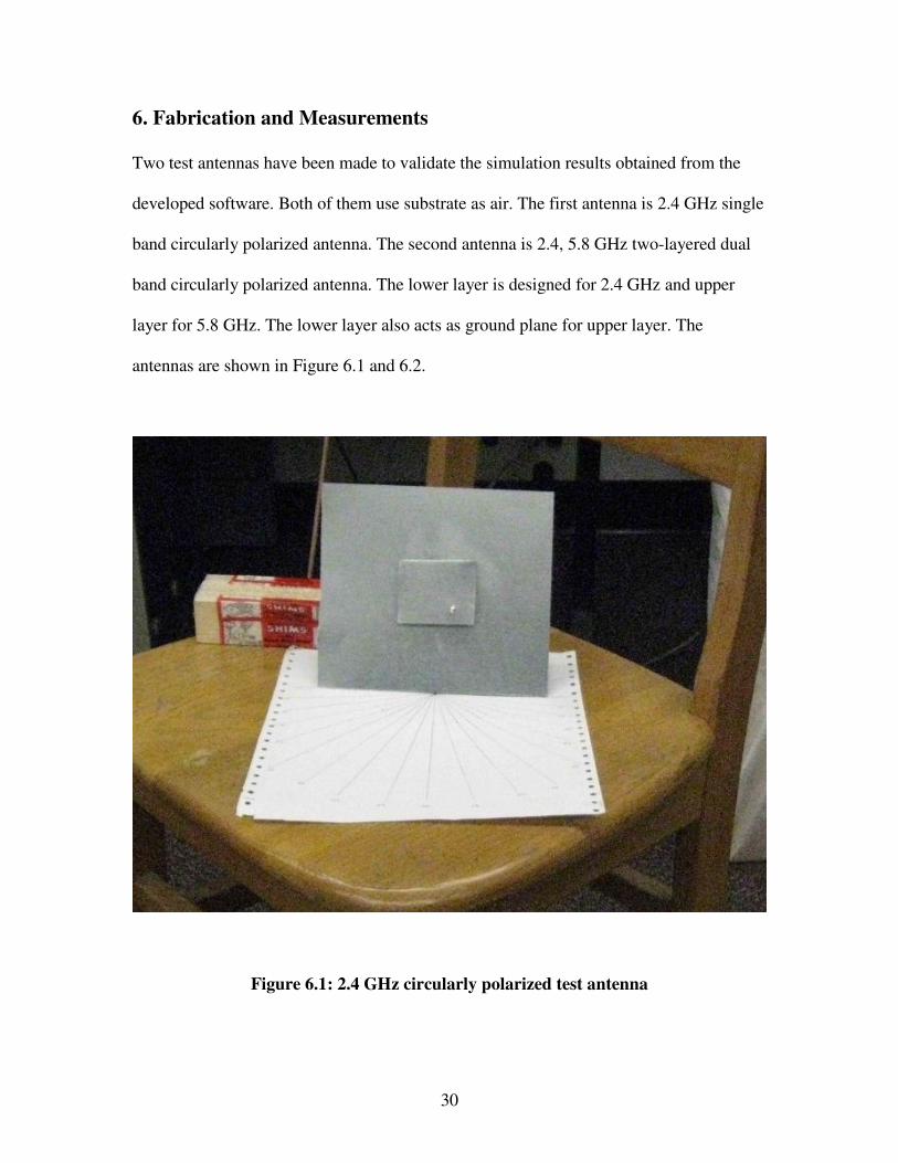
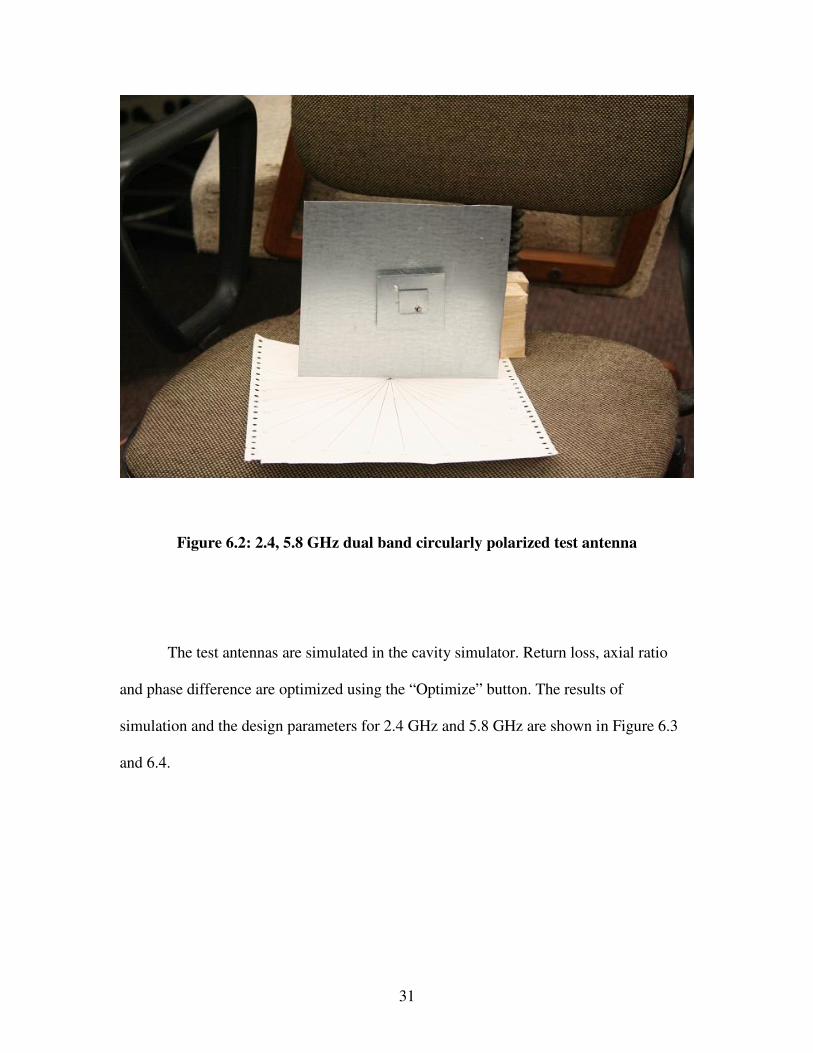
6. Fabrication and Measurements
Two test antennas have been made to validate the simulation results obtained from the
developed software. Both of them use substrate as air. The first antenna is 2.4 GHz single
band circularly polarized antenna. The second antenna is 2.4, 5.8 GHz two-layered dual
band circularly polarized antenna. The lower layer is designed for 2.4 GHz and upper
layer for 5.8 GHz. The lower layer also acts as ground plane for upper layer. The
antennas are shown in Figure 6.1 and 6.2.
Figure 6.1: 2.4 GHz circularly polarized test antenna
31
Figure 6.2: 2.4, 5.8 GHz dual band circularly polarized test antenna
The test antennas are simulated in the cavity simulator. Return loss, axial ratio
and phase difference are optimized using the “Optimize” button. The results of
simulation and the design parameters for 2.4 GHz and 5.8 GHz are shown in Figure 6.3
and 6.4.

32
Figure 6.3 Simulation of 2.4 GHz band

33
Figure 6.4 Simulation of 5.8 GHz band
34
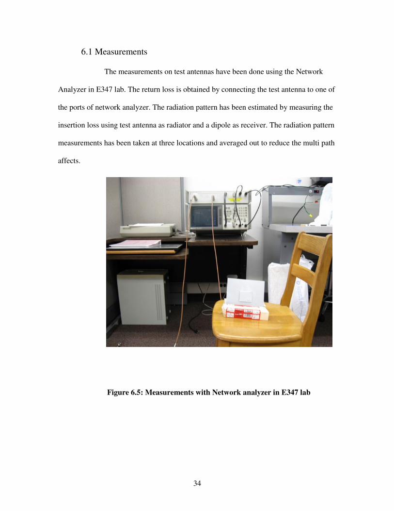
6.1 Measurements
The measurements on test antennas have been done using the Network
Analyzer in E347 lab. The return loss is obtained by connecting the test antenna to one of
the ports of network analyzer. The radiation pattern has been estimated by measuring the
insertion loss using test antenna as radiator and a dipole as receiver. The radiation pattern
measurements has been taken at three locations and averaged out to reduce the multi path
affects.
Figure 6.5: Measurements with Network analyzer in E347 lab

35
Figure 6.6: Return Loss Measurement with network analyzer in E347 lab
The circular polarization has been measured by taking the radiation pattern
readings in two orthogonal positions of antennas as shown in Figure 6.6. All the
measurement data is available in Appendices A1 to B3.
Figure 6.7: Measurement for circular polarization
36
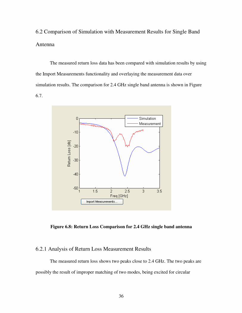
6.2 Comparison of Simulation with Measurement Results for Single Band
Antenna
The measured return loss data has been compared with simulation results by using
the Import Measurements functionality and overlaying the measurement data over
simulation results. The comparison for 2.4 GHz single band antenna is shown in Figure
6.7.
Figure 6.8: Return Loss Comparison for 2.4 GHz single band antenna
6.2.1 Analysis of Return Loss Measurement Results
The measured return loss shows two peaks close to 2.4 GHz. The two peaks are
possibly the result of improper matching of two modes, being excited for circular
37
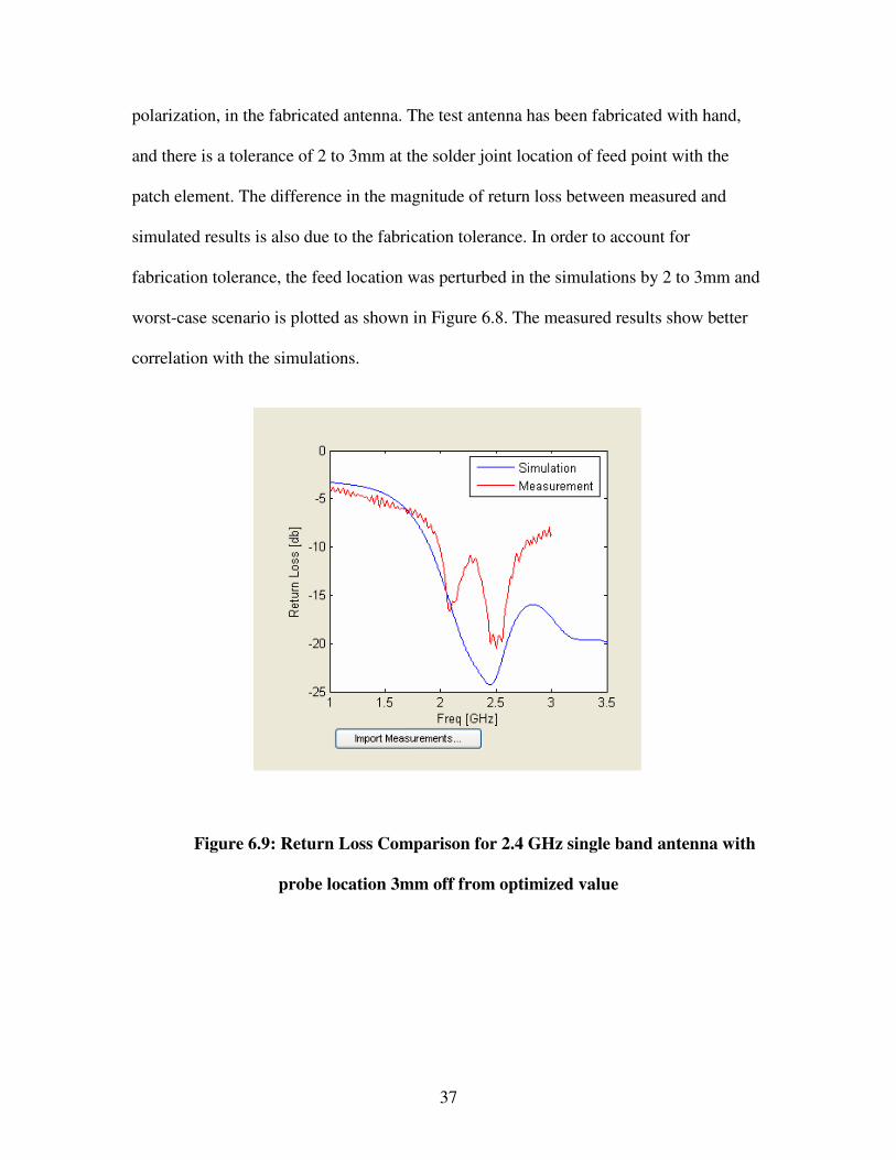
polarization, in the fabricated antenna. The test antenna has been fabricated with hand,
and there is a tolerance of 2 to 3mm at the solder joint location of feed point with the
patch element. The difference in the magnitude of return loss between measured and
simulated results is also due to the fabrication tolerance. In order to account for
fabrication tolerance, the feed location was perturbed in the simulations by 2 to 3mm and
worst-case scenario is plotted as shown in Figure 6.8. The measured results show better
correlation with the simulations.
Figure 6.9: Return Loss Comparison for 2.4 GHz single band antenna with
probe location 3mm off from optimized value

38
6.2.2 Comparison of radiation pattern results
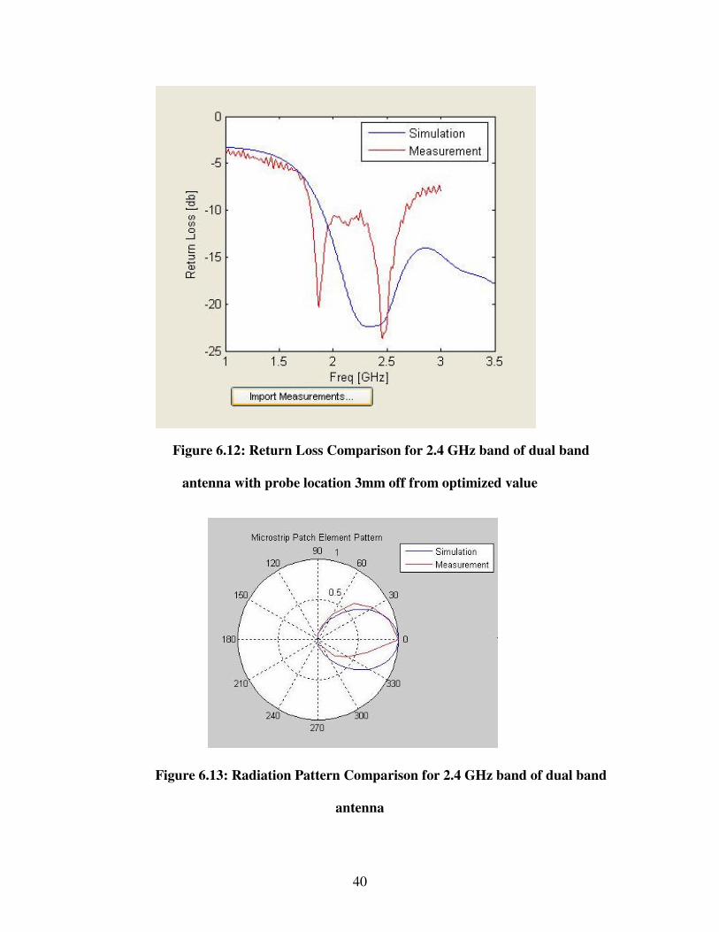
The radiation pattern measurements taken in db, at multiple locations are
averaged out and converted to normalized fraction values to overlay on simulation results
on polar plots. Figure 6.9 shows the comparison of measured values with simulation
values. The comparison shows close agreement.
Figure 6.10: Radiation Pattern Comparison for 2.4 GHz single band antenna
The measured axial ratio is plotted in db by taking the difference between
the radiation values for the two orthogonal positions of antenna as illustrated in Figure
6.6. The measured axial ratio for 2.4 GHz single band antenna is shown in Figure 6.10.
The axial ratio is close to 6db instead of 0db. This is also attributed to improper matching
of two modes, being excited for circular polarization due to fabrication tolerance.

39
Figure 6.11: Measured Axial Ratio for 2.4 GHz single band antenna
6.3 Comparison of Simulation with Measurement Results for Dual Band
Antenna
The measurements for dual band antenna have been done for both bands in a manner
similar to single band antenna. The return loss, radiation pattern and axial ratio for both
bands are shown in Figure 6.11 to Figure 6.16. The comparisons for results are similar as
for 2.4 GHz antenna, with one exception. The resonance for 5.8 GHz antenna is closer to
5.5 GHz. One reason for shift in resonance is the fabrication tolerance mentioned in
previous section. Another possible reason is that the ground plane for 5.8 GHz patch is
2.4 GHz patch, which is relatively small and is not large enough to assume infinite. The
simulations however do not take into account the finite ground plane affects.
40
Figure 6.12: Return Loss Comparison for 2.4 GHz band of dual band
antenna with probe location 3mm off from optimized value
Figure 6.13: Radiation Pattern Comparison for 2.4 GHz band of dual band
antenna
41
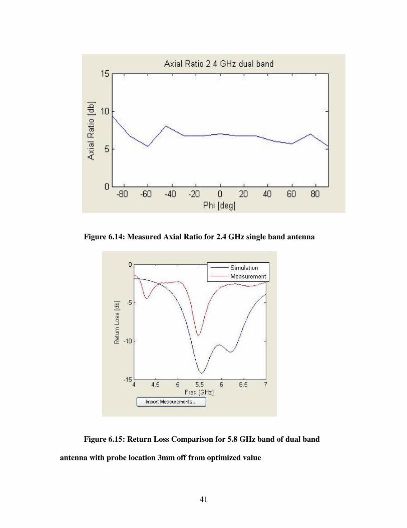
Figure 6.14: Measured Axial Ratio for 2.4 GHz single band antenna
Figure 6.15: Return Loss Comparison for 5.8 GHz band of dual band
antenna with probe location 3mm off from optimized value

42
Figure 6.16: Radiation Pattern Comparison for 5.8 GHz band of dual band
antenna
Figure 6.17: Measured Axial Ratio for 5.8 GHz single band antenna

43
7. Conclusions
In this project, a Matlab GUI based simulation software to simulate microstrip patch
antennas has been developed.
a) The simulation software has ability to predict return loss, radiation pattern
and circular polarization
b) The simulation software can be used to design dual band antennas.
c) The simulation software allows simulation of antenna arrays
A single band antenna and a dual band antenna have been fabricated, and return loss and
radiation pattern measurements have been done. The measurement results agree with
simulation results within the limitations of fabrication method used.

44
8. Future Work
The work done in this project can be extended in multiple ways.
a) The simulations for dual band antennas can be improved by accounting for the
finite ground plane affects.
b) The radiation patterns plotted are for one particular mode. The software should
allow user to select the mode and it should then plot the radiation pattern for that
mode
c) The software can allow plotting the input impedance on Smith Chart.

45
REFERENCES
[1] Lo, Y. T., Solomon, D., and Richards W.F., ‘Theory and Experiment on Microstrip
antennas.’ IEEE Trans. on AP, 1979, Vol. AP-27, pp. 137 – 149.
[2] Richards W.F., Lo, Y. T., and Harrison D. D., ‘An Improved theory for Microstrip
antennas and Application.’ IEEE Trans. on AP, 1981, Vol. AP-29, pp. 38 – 46.
[3] Garg, R., Bhartia, P., Bahl, I., and Ittipiboon, A., Microstrip Antenna Design
Handbook, Artech House, Inc, 2001.
[4] Stutzman, W.L., and Thiele, G.A., Antenna Theory and Design, John Wiley &
Sons, Inc, 1998.
[5] Balanis, C.A., Antenna Theory, Analysis and Design, John Wiley & Sons, Inc,
1997.
[6] Pozar, D. M., Microwave Engineering, Second Edition, JohnWiley & Sons, Inc,
1988.
[7] Gan, Yeow-Beng, Chua Chee-Parng, and Li, Le-Wei , An enhanced cavity model for
microstrip antennas, Microwave and optical technology letters, vol. 40, no. 6, March 20
2004, pp. 520 – 523.
[8] Thouroude, D., Himdi , M. and Daniel, J. P., CAD-Oriented Cavity Model For
Rectangular Patches, Electronics Letters 2lst June 1990 Vol. 26 No. 13, pp. 842 - 844
[9] D. D. Sandu, O. G. Avadanei, A. Ioachima, D. Ionesi, Contribution To The Cavity
Model For Analysis of Microstrip patch antennas, Journal of Optoelectronics and
advanced materials vol. 8, no. 1, Febraury 2006, p. 339 – 344
[10] Martin, N. M., Improved cavity model parameters for calculation of resonant
frequency of rectangular microstrip antennas, Electronic Letters, 26th
May 1988, Vol. 24,
No. 11, pp. 680-681
[11] Deshpande, M. D., Bailey, M. C., Input impedance of microstrip antennas, IEEE
transactions on antennas and propagation, vol. Ap-30, no. 4, July 1982, pp. 645 – 650
[12] James, J.R. and Hall, P.S., Handbook of Microstrip Antennas, Vols 1 and 2, Peter
Peregrinus, London, UK, 1989.
[13] Bancroft, Randy, Microstrip and Printed Antenna Design, 2nd
Edition, SciTech
Publishing Inc., 2009

46
[14] Pozar, D. M. and Schaubert, D. H., Microstrip Antennas, The Analysis and Design
of Microstrip Antennas and Arrays, IEEE Press, 1995
[15] Derneryd, A. G. and Lind, A. G., Extended Analysis of Rectangular Microstrip
Resonator Antennas, IEEE transactions on antennas and propagation, Vol. AP-27, No. 6,
November 1979, pp. 846 – 849
[16] Hammerstad, E. O., Equations for microstrip circuit design, Proc. Fifth European
Microwave Conf., pp. 268-272, September 1975.