DESIGN AND ANALYSIS OF FAST LOW POWER...
153
DESIGN AND ANALYSIS OF FAST LOW POWER SRAMs A DISSERTATION SUBMITTED TO THE DEPARTMENT OF ELECTRICAL ENGINEERING AND THE COMMITTEE ON GRADUATE STUDIES OF STANFORD UNIVERSITY IN PARTIAL FULFILLMENT OF THE REQUIREMENTS FOR THE DEGREE OF DOCTOR OF PHILOSOPHY Bharadwaj S. Amrutur August 1999
Transcript of DESIGN AND ANALYSIS OF FAST LOW POWER...
DESIGN AND ANALYSIS OF FAST LOW POWER
SRAMs
A DISSERTATION
SUBMITTED TO THE DEPARTMENT OF
ELECTRICAL ENGINEERING
AND THE COMMITTEE ON GRADUATE STUDIES
OF STANFORD UNIVERSITY
IN PARTIAL FULFILLMENT OF THE REQUIREMENTS
FOR THE DEGREE OF
DOCTOR OF PHILOSOPHY
Bharadwaj S. Amrutur
August 1999

ii
© Copyright by Bharadwaj S. Amrutur 1999
All Rights Reserved

ate,
ate,
ate,
I certify that I have read this dissertation and that in my opinion it is fully adequ
in scope and quality, as a dissertation for the degree of Doctor of Philosophy.
I certify that I have read this dissertation and that in my opinion it is fully adequ
in scope and quality, as a dissertation for the degree of Doctor of Philosophy.
I certify that I have read this dissertation and that in my opinion it is fully adequ
in scope and quality, as a dissertation for the degree of Doctor of Philosophy.
Approved for the University Committee on Graduate Studies:
Mark A. Horowitz (Principal Advisor)
Bruce A. Wooley
Krishna Saraswat
iii

iv
Abstract
ories
into
line
hs are
mal
r, is
tting
ower.
with
izing.
n the
.
ings
sense
f their
This thesis explores the design and analysis of Static Random Access Mem
(SRAMs), focusing on optimizing delay and power. The SRAM access path is split
two portions: from address input to word line rise (the row decoder) and from word
rise to data output (the read data path). Techniques to optimize both of these pat
investigated.
We determine the optimal decoder structure for fast low power SRAMs. Opti
decoder implementations result when the decoder, excluding the predecode
implemented as a binary tree. We find that skewed circuit techniques with self rese
gates work the best and evaluate some simple sizing heuristics for low delay and p
We find that the heuristic of using equal fanouts of about 4 per stage works well even
interconnect in the decode path, provided the interconnect delay is reduced by wire s
For fast lower power solutions, the heuristic of reducing the sizes of the input stage i
higher levels of the decode tree allows for good trade-offs between delay and power
The key to low power operation in the SRAM data path is to reduce the signal sw
on the high capacitance nodes like the bitlines and the data lines. Clocked voltage
amplifiers are essential for obtaining low sensing power, and accurate generation o
v
limit
cked
plica
ating
and
s the
scal-
to an
delay
cess
e wire
ough
lay for
sense clock is required for high speed operation. We investigate tracking circuits to
bitline and I/O line swings and aid in the generation of the sense clock to enable clo
sense amplifiers. The tracking circuits essentially use a replica memory cell and a re
bitline to track the delay of the memory cell over a wide range of process and oper
conditions. We present experimental results from two different prototypes.
Finally we look at the scaling trends in the speed and power of SRAMs with size
technology and find that the SRAM delay scales as the logarithm of its size as long a
interconnect delay is negligible. Non-scaling of threshold mismatches with process
ing, causes the signal swings in the bitlines and data lines also not to scale, leading
increase in the relative delay of an SRAM, across technology generations.The wire
starts becoming important for SRAMs beyond the 1Mb generation. Across pro
shrinks, the wire delay becomes worse, and wire redesign has to be done to keep th
delay in the same proportion to the gate delay. Hierarchical SRAM structures have en
space over the array for using fat wires, and these can be used to control the wire de
4Mb and smaller designs across process shrinks.
vi

Acknowledgments
the
on for
sup-
nid
hna
reatly
aining
anks
ny a
Wei,
Ken
rable
vin,
fam-
my
par-
m.
I thank my advisor Prof. Mark Horowitz for his invaluable guidance throughout
course of this thesis. His insights and wisdom have been a great source of inspirati
this work. I thank my co-advisor Prof. Bruce Wooley for his quiet encouragement and
port during my stay in Stanford. I am grateful to Prof. Teresa Meng and Prof. Leo
Kazovsky for agreeing to be a part of my orals committee. I am indebted to Prof. Kris
Saraswat for reading my dissertation at a very short notice. The dissertation has g
benefited from the astute comments of the reading committee members and any rem
errors are solely my own.
The many hours I have spent at work have been very stimulating and enriching, th
to the wonderful students I have been privileged to interact with. I have enjoyed ma
conversation with the inhabitants of CIS and would especially like to thank Guyeon
Dan Weinlader, Chih-Kong Ken Yang, Ricardo Gonzalez, Stefanos Sidiropoulos,
Mai, Toshihiko Mori, Ron Ho, Vijayaraghavan Soundararajan and Esin Terzioglu.
Thanks to my many friends on campus and outside, I have had many memo
moments outside my work. I would especially like to thank Suhas, Navakant, Bijit, Na
Anil, Mohan and Shankar.
I am grateful to Sudha, Anand, Raghavan and Meera for being such a wonderful
ily. I thank my wife, Vidya, for her love and patience during the final stages of
dissertation. Last but not the least, I am eternally indebted to by grandfather and my
ents for their love, encouragement and support. This dissertation is dedicated to the
vii

viii

List of Tables
cal...31
tical....34
...34
.....35
in % ......35
...52
.....65
.....66
.....69
8
82
31
....132
Table 3.1: Efforts and delays for three sizing techniques relative to the theoretilower bound. Fanout of first chain f1 = 3.84 for all cases....................
Table 3.2: Relative delays with the two sizing heuristics compared to the theorelower bound.........................................................................................
Table 3.3: Relative delays for a 1Mb SRAM with different wire sizes.................
Table 3.4: Relative power of various components of the decode path in%.........
Table 3.5: Relative delay of various components of the decode path under H1 .............................................................................................................
Table 3.6: Delay and Power Comparisons of Various Circuit Styles in 0.25µm pro-cess at 2.5V. Delay of a fanout 4 loaded inverter is 90pS....................
Table 4.1: Block parameters: 256 rows, 64 columns...........................................
Table 4.2: Block parameters: 64 rows, 32 columns.............................................
Table 4.3: Block parameters: 256 rows, 64 columns...........................................
Table 4.4: Measurement Data for the 1.2µm prototype chip....................................7
Table 4.5: Measured data for the 0.35µm prototype ................................................
Table C.1: Features of the base 0.25µm technology ...............................................1
Table C.2: Technology scaling of some parameters............................................
xii
List of Figures
.....2
...6
.......8
....9
.....10
...11
tch....13
....15
....17
.....18
r
...22
....24
....25
...29
....32
full....37
Figure 1.1: Elementary SRAM structure with the cell design in its inset ...........
Figure 2.1: Divided Word Line (DWL) Architecture............................................
Figure 2.2: Schematic of a two-level 8 to 256 decoder .....................................
Figure 2.3: a) Conventional static NAND gate b) Nakamura’s NAND gate [23]
Figure 2.4: Skewed NAND gate........................................................................
Figure 2.5: Bitline mux hierarchies in a 512 row block ......................................
Figure 2.6: Two common types of sense amplifiers, a) current mirror type, b) latype...................................................................................................
Figure 3.1: Critical path of a decoder in a large SRAM.....................................
Figure 3.2: A chain of inverters to drive a load ..................................................
Figure 3.3: RC model of a inverter....................................................................
Figure 3.4: Critical path in a 4 to 16predecoder. The path is highlighted by thickelines. The sizes of the gates and their logical effort along with thebranching efforts of two intermediate nodes is shown......................
Figure 3.5: Buffer chain with intermediate interconnect....................................
Figure 3.6: Modeling the interconnect delay......................................................
Figure 3.7: (a) Schematic of Embedded SRAMs (b) Equivalent critical path ....
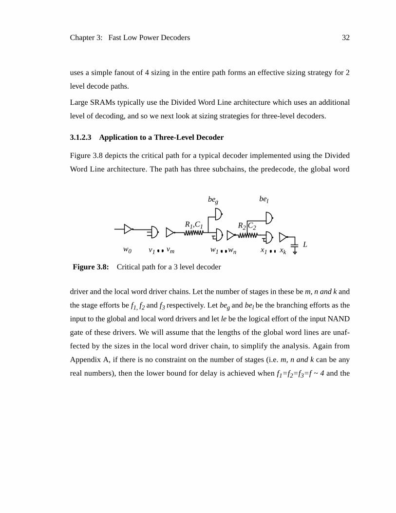
Figure 3.8: Critical path for a 3 level decoder....................................................
Figure 3.9: Delay energy performance of the three sizing heuristics and theircomparison to optimal delay energy trade-off curve. (a) shows the graph (b) shows the same graph magnified along the X axis...........
xiii
.
t....39
...40
....41
)....43
.....44
....45
.....46
g.48
....49
....50
S....51
.....53
......56
....57
.....59
...59
y.....60
um....61
rol ..
....63
.....68
....69
...70
......72
....73
....74
.....74
....75
Figure 3.10: SRCMOS resetting technique, a) self-reset b) predicated self-rese
Figure 3.11: A DRCMOS Technique to do local self-resetting of a skewed gate
Figure 3.12: Chain of maximally skewed inverters..............................................
Figure 3.13: Static 2 input NAND gate for a pulsed decoder: (a) Non-skewed (bSkewed and (c) Clocked ..................................................................
Figure 3.14: Source Coupled NAND gate...........................................................
Figure 3.15: Comparison of delay of the source coupled NAND gate.................
Figure 3.16: NOR style decoder [21] ..................................................................
Figure 3.17: 4 to 16 predecoder in conventional series nfet style with no skewin
Figure 3.18: Critical path for 4 to 16 decoder in conventional static style withskewing ............................................................................................
Figure 3.19: NOR style predecoder with no skewing ..........................................
Figure 3.20: NOR style 4 to 16 predecoder with maximal skewing and DRCMOresetting............................................................................................
Figure 3.21: Schematic of fast low power 3 level decoder structure...................
Figure 4.1: Common sense clock generation techniques .................................
Figure 4.2: Delay matching of inverter chain delay stage with respect to bitlinedelay.................................................................................................
Figure 4.3: Latch type sense amplifier ..............................................................
Figure 4.4: Replica column with bitline capacitance ratioing.............................
Figure 4.5: Comparison of delay matching of replica versus inverter chain delaelements ..........................................................................................
Figure 4.6: Matching comparisons over varying cell threshold offsets in a 0.25@ 1.2V.............................................................................................
Figure 4.7: Control circuits for sense clock activation and word line pulse cont62
Figure 4.8: Delay matching of two buffer chains ...............................................
Figure 4.9: Current Ratio Based Replica Structure...........................................
Figure 4.10: Skewed word line driver ..................................................................
Figure 4.11: Control circuits for current ratio based replica circuit ......................
Figure 4.12: Replica Structure Placement ..........................................................
Figure 4.13: Column I/O circuits..........................................................................
Figure 4.14: Pulsed Global word line driver ........................................................
Figure 4.15: Level to pulse converter ..................................................................
Figure 4.16: Global I/O circuits............................................................................
xiv
.
76
s..77
....78
0
..81
e...83
...85
ng....87
....93
....97
....97
....98
.100
...101
..104
06
.....
...111
Figure 4.17: Die photo of a 1.2µm prototype chip...................................................
Figure 4.18: Waveforms on a bitline pair during an alternating read/write accespattern, obtained via direct probing of the bitline wires on the chip.
Figure 4.19: On-chip probed data line waveforms for an alternating read/writepattern ..............................................................................................
Figure 4.20: Die photo of a prototype chip in 0.25µm technology ..........................8
Figure 4.21: Architecture of a prototype chip in 0.25µm CMOS ............................81
Figure 4.22: Modified Global Word line Driver.....................................................
Figure 4.23: Measured energy (black squares) versus supply. Also shown is thquadratic curve fit on the 0.5V and the 1V points. ...........................
Figure 4.24: a) Schematic of cells for low swing writes b) waveforms ................
Figure 4.25: On chip probed wave forms of bitlines for low swing writes alternatiwith reads. ........................................................................................
Figure 5.1: Array partitioning example ..............................................................
Figure 5.2: Area estimation for the word drivers ...............................................
Figure 5.3: a) Current source driving a RCπ network. b) Sketch of the nodewaveforms........................................................................................
Figure 5.4: Bitline circuit ...................................................................................
Figure 5.5: Bitline delay versus column height; 0.25µm, 1.8V and 4 columnsmultiplexing ......................................................................................
Figure 5.6: Local sense amplifier structure .......................................................
Figure 5.7: Area estimation of the output mux...................................................
Figure 5.8: Delay scaling with size in 0.25µm process........................................1
Figure 5.9: Delay versus technology for different wire widths for a 4Mb SRAM107
Figure 5.10: Delay versus Area for a 4Mb SRAM in 0.25µm process ..................109
Figure 5.11: Delay and Area versus block height for a 4Mb SRAM in a 0.25µmprocess.............................................................................................
Figure 5.12: Energy versus Delay for a 4Mb SRAM in 0.25µm process ..............112
xv

.
xvi
Chapter
is is
each
e main
ation
plosive
Ms,
ling
ircuit
wer
atrix
air
ted to
rite
s. The
to m
umn
ually
to the
1 Introduction
Fast low power SRAMs have become a critical component of many VLSI chips. Th
especially true for microprocessors, where the on-chip cache sizes are growing with
generation to bridge the increasing divergence in the speeds of the processor and th
memory [1-2]. Simultaneously, power dissipation has become an important consider
both due to the increased integration and operating speeds, as well as due to the ex
growth of battery operated appliances [3]. This thesis explores the design of SRA
focusing on optimizing delay and power. While process [4-5] and supply [6-11] sca
remain the biggest drivers of fast low power designs, this thesis investigates some c
techniques which can be used in conjunction to scaling to achieve fast, low po
operation.
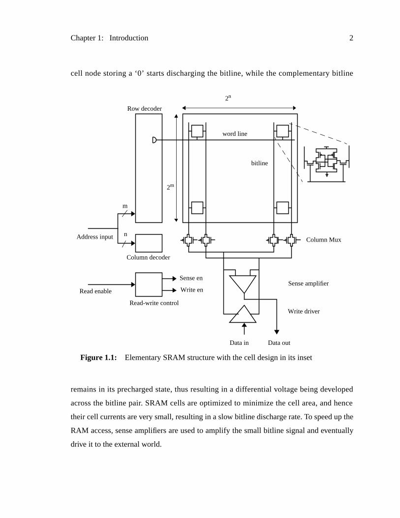
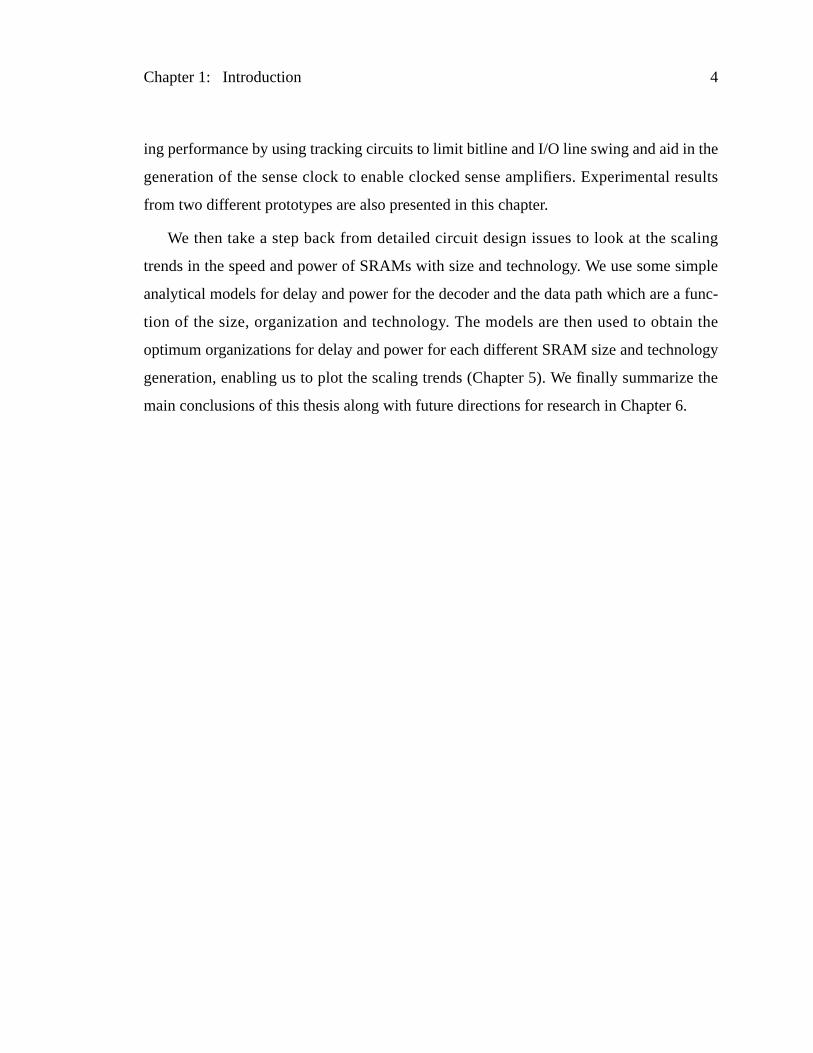
Conceptually, an SRAM has the structure shown in Figure 1.1. It consists of a m
of 2m rows by 2n columns of memory cells. Each memory cell in an SRAM contains a p
of cross coupled inverters which form a bi-stable element. These inverters are connec
a pair of bitlines through nMOS pass transistors which provide differential read and w
access. An SRAM also contains some column and row circuitry to access these cell
m+n bits of address input, which identifies the cell which is to be accessed, is split in
row address bits and n column address bits. The row decoder activates one of the 2m word
lines which connects the memory cells of that row to their respective bitlines. The col
decoder sets a pair of column switches which connects one of 2n bitline columns to the
peripheral circuits.
In a read operation, the bitlines start precharged to some reference voltage us
close to the positive supply. When word line turns high, the access nfet connected
1
Chapter 1: Introduction 2
line
oped
nce
p the
tually
cell node storing a ‘0’ starts discharging the bitline, while the complementary bit
remains in its precharged state, thus resulting in a differential voltage being devel
across the bitline pair. SRAM cells are optimized to minimize the cell area, and he
their cell currents are very small, resulting in a slow bitline discharge rate. To speed u
RAM access, sense amplifiers are used to amplify the small bitline signal and even
drive it to the external world.
Sense amplifier
Data outData in
Write driver
Row decoder
Column MuxAddress input
Column decoder
Read enable
Sense en
Write en
Read-write control
word line
bitline
m
n
2n
2m
Figure 1.1: Elementary SRAM structure with the cell design in its inset

Chapter 1: Introduction 3
driv-
the
cess
itline
and
d lay-
ists
ed and
AMs
timiza-
m the
ports
style
buff-
and
rcon-
d to
heu-
uit
ir delay
code
nse
ess
hurt-
During a write operation, the write data is transferred to the desired columns by
ing the data onto the bitline pairs by grounding either the bit line or its complement. If
cell data is different from the write data, then the ‘1’ node is discharged when the ac
nfet connects it to the discharged bitline, thus causing the cell to be written with the b
value.
The basic SRAM structure can be significantly optimized to minimize the delay
power at the cost of some area overhead. The optimization starts with the design an
out of the RAM cell, which is undertaken in consultation with the process technolog
[4]. For the most part, the thesis assumes that a ram cell has been adequately design
looks at how to put the cells together efficiently.
The next chapter introduces the various techniques which are used in practical SR
and motivates the issues addressed by this thesis. For the purposes of design and op
tion, the access path can be divided into two portions: the row decoder - the path fro
address inputs to the word line, and the data path - the portion from the memory cell
to the SRAM I/O ports.
The decoder design problem has two major tasks: determining the optimal circuit
and decode structure and finding the optimal sizes for the circuits and the amount of
ering at each level. The problem of optimally sizing a chain of gates for optimal delay
power is well understood [12-16]. Since the decode path also has intermediate inte
nect, we will analyze the optimal sizing problem in this context. The analysis will lea
some formulae for bounding the decoder delay and allow us to evaluate some simple
ristics for doing the sizing in practical situations. We will then look at various circ
techniques that have been proposed to speed up the decode path and analyze the
and power characteristics. This will eventually enable us to sketch the optimal de
structures to achieve fast and low power operation (Chapter 3).
In the SRAM data path, switching of the bitlines and I/O lines and biasing the se
amplifiers consume a significant fraction of the total power, especially in wide acc
width memories. Chapter 4 investigates techniques to reduce SRAM power without
Chapter 1: Introduction 4
the
esults
aling
imple
func-
n the
logy
e the
.
ing performance by using tracking circuits to limit bitline and I/O line swing and aid in
generation of the sense clock to enable clocked sense amplifiers. Experimental r
from two different prototypes are also presented in this chapter.
We then take a step back from detailed circuit design issues to look at the sc
trends in the speed and power of SRAMs with size and technology. We use some s
analytical models for delay and power for the decoder and the data path which are a
tion of the size, organization and technology. The models are then used to obtai
optimum organizations for delay and power for each different SRAM size and techno
generation, enabling us to plot the scaling trends (Chapter 5). We finally summariz
main conclusions of this thesis along with future directions for research in Chapter 6
Chapter
inno-
these
rious
hich
d by
lithic
enti-
of the
ly to
cros,
f as
g an
d sub
ks for
s the
2 Overview of CMOSSRAMs
The delay and power of practical SRAMs have been reduced over the years via
vations in the array organization and circuit design. This chapter discusses both
topics and highlights the issues addressed by this thesis. We will first explore the va
partitioning strategies in Section 2.1 and then point out the main circuit techniques w
have been presented in the literature to improve speed and power (Section 2.2).
2.1 SRAM Partitioning
For large SRAMs, significant improvements in delay and power can be achieve
partitioning the cell array into smaller sub arrays, rather than having a single mono
array as shown in Figure 1.1. Typically, a large array is partitioned into a number of id
cally sized sub arrays (commonly referred to as macros), each of which stores a part
accessed word, called the sub word, and all of which are activated simultaneous
access the complete word [20-22]. High performance SRAMs can have up to 16 ma
while low power SRAMs typically have only one macro. The macros can be thought o
independent RAMs, except that they might share parts of the decoder.
Each macro conceptually looks like the basic structure shown in Figure 1.1. Durin
access to some row, the word line activates all the cells in that row and the desire
word is accessed via the column multiplexers. This arrangement has two drawbac
macros that have a very large number of columns: the word line RC delay grows a
5
Chapter 2: Overview of CMOS SRAMs 6
ber
acros
ed
nal
ucing
ving
e is
al to
mns
square of the number of cells in the row, and bitline power grows linearly with the num
of columns. Both these drawbacks can be overcome by further sub dividing the m
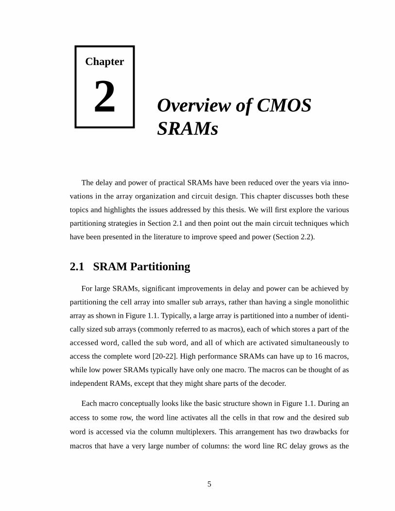
into smaller blocks of cells using the Divided Word Line (DWL) technique first propos
by Yoshimoto, et.al. in [17]. In the DWL technique the long word line of a conventio
array is broken up into k sections, with each section activated independently thus red
the word line length by k and hence reducing its RC delay by k2. Figure 2.1 shows the
DWL architecture where a macro of 256 columns is partitioned into 4 blocks each ha
only 64 columns. The row selection is now done in two stages, first a global word lin
activated which is then transmitted into the desired block by a block select sign
activate the desired local word line. Since the local word line is shorter (only 64 colu
dout din
address
bitlines
global senseamp
I/O lineslocal senseamp
local
word line
global
word line
blockselect
Figure 2.1: Divided Word Line (DWL) Architecture
64
Chapter 2: Overview of CMOS SRAMs 7
the
itive
f the
ider
or of
the
all the
This
line
ding
nd is
. For
rs at
the
5 we
nd the
d line.
tic of
wide), it has a lower RC delay. Though the global word line still is nearly as long as
width of the macro, it has a lower RC delay than a full length word line since its capac
loading is smaller. It sees only the input loading of the four word line drivers instead o
loading of all the 256 cells. In addition, its resistance can be lower as it could use w
wires on a higher level metal layer. The word line RC delay is reduced by another fact
four by keeping the word drivers in the center of the word line segments thus halving
length of each segment. Since 64 cells within the block are activated as opposed to
256 cells in the undivided array, the column current is also reduced by a factor 4.
concept of dividing the word line can be carried out recursively on the global word
(and the block select line) for large RAMs, and is called the Hierarchical Word Deco
(HWD) technique [45]. Partitioning can also be done to reduce the bitline heights a
discussed further in the next section.
Partitioning of the RAM incurs area overhead at the boundaries of the partitions
example, a partition which dissects the word lines requires the use of word line drive
the boundary. Since the RAM area determines the lengths of the global wires in
decoder and the data path, it directly influences their delay and energy. In Chapter
will study the trade offs in delay, energy and area obtained via partitioning.
2.2 Circuit techniques in SRAMs
The SRAM access path can be broken down into two components: the decoder a
data path. The decoder encompasses the circuits from the address input to the wor
The data path encompasses the circuits from the cells to the I/O ports.
The logical function of the decoder is equivalent to 2n n-input AND gates, where the
large fan-in AND operation is implemented in an hierarchical structure. The schema
Chapter 2: Overview of CMOS SRAMs 8
here
the
e
gate
ires.
the
izing
g has
ower
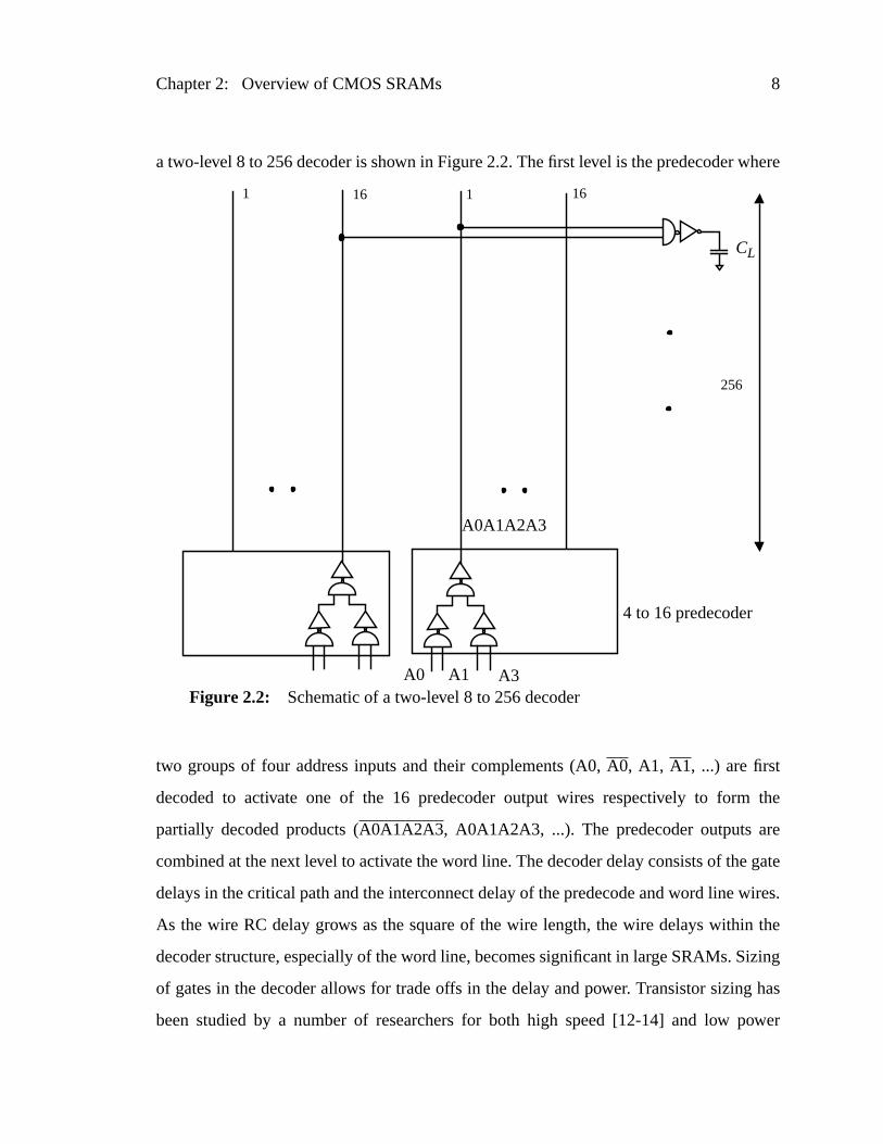
a two-level 8 to 256 decoder is shown in Figure 2.2. The first level is the predecoder w
two groups of four address inputs and their complements (A0,A0, A1, A1, ...) are first
decoded to activate one of the 16 predecoder output wires respectively to form
partially decoded products (A0A1A2A3, A0A1A2A3, ...). The predecoder outputs ar
combined at the next level to activate the word line. The decoder delay consists of the
delays in the critical path and the interconnect delay of the predecode and word line w
As the wire RC delay grows as the square of the wire length, the wire delays within
decoder structure, especially of the word line, becomes significant in large SRAMs. S
of gates in the decoder allows for trade offs in the delay and power. Transistor sizin
been studied by a number of researchers for both high speed [12-14] and low p
CL
1 161 16
256
4 to 16 predecoder
Figure 2.2: Schematic of a two-level 8 to 256 decoderA0 A1 A3
A0A1A2A3
Chapter 2: Overview of CMOS SRAMs 9
e of
apter
s for
d to
n in a
uch
w
e new
of the
it is
falling
ircuit
hich
ss all
row
[15-16]. The decoder sizing problem is complicated slightly due to the presenc
intermediate interconnect from the predecode wires. We examine this problem in Ch
3 and provide lower bounds for delay. We also evaluate some simple sizing heuristic
obtaining high speed and low power operation.
The decoder delay can be greatly improved by optimizing the circuit style use
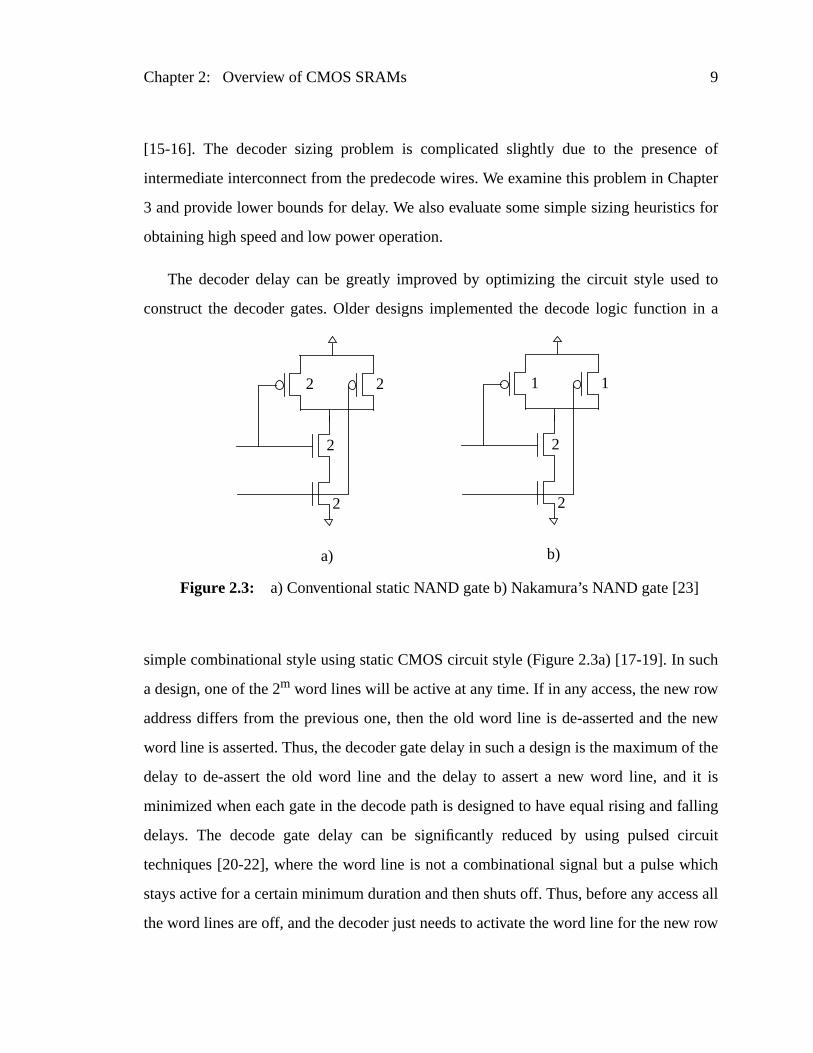
construct the decoder gates. Older designs implemented the decode logic functio
simple combinational style using static CMOS circuit style (Figure 2.3a) [17-19]. In s
a design, one of the 2m word lines will be active at any time. If in any access, the new ro
address differs from the previous one, then the old word line is de-asserted and th
word line is asserted. Thus, the decoder gate delay in such a design is the maximum
delay to de-assert the old word line and the delay to assert a new word line, and
minimized when each gate in the decode path is designed to have equal rising and
delays. The decode gate delay can be significantly reduced by using pulsed c
techniques [20-22], where the word line is not a combinational signal but a pulse w
stays active for a certain minimum duration and then shuts off. Thus, before any acce
the word lines are off, and the decoder just needs to activate the word line for the new
2
2
2 2
a) b)
2
2
1 1
Figure 2.3: a) Conventional static NAND gate b) Nakamura’s NAND gate [23]
Chapter 2: Overview of CMOS SRAMs 10
r logic
n and
re the
the
n the
ucing
. This
letely
re the
once
ready
an be
wer
static
nly a
nother
address. Since only one kind of transition needs to propagate through the decode
chain, the transistor sizes in the gates can be skewed to speed up this transitio
minimize the decode delay. Figure 2.3b shows an instance of this technique [23] whe
pMOS in the NAND gates are sized to be half that in a regular NAND structure. In
pulsed design, the pMOS sizes can be reduced by a factor of two and still result i
same rising delay since it is guaranteed that both the inputs will de-assert, thus red
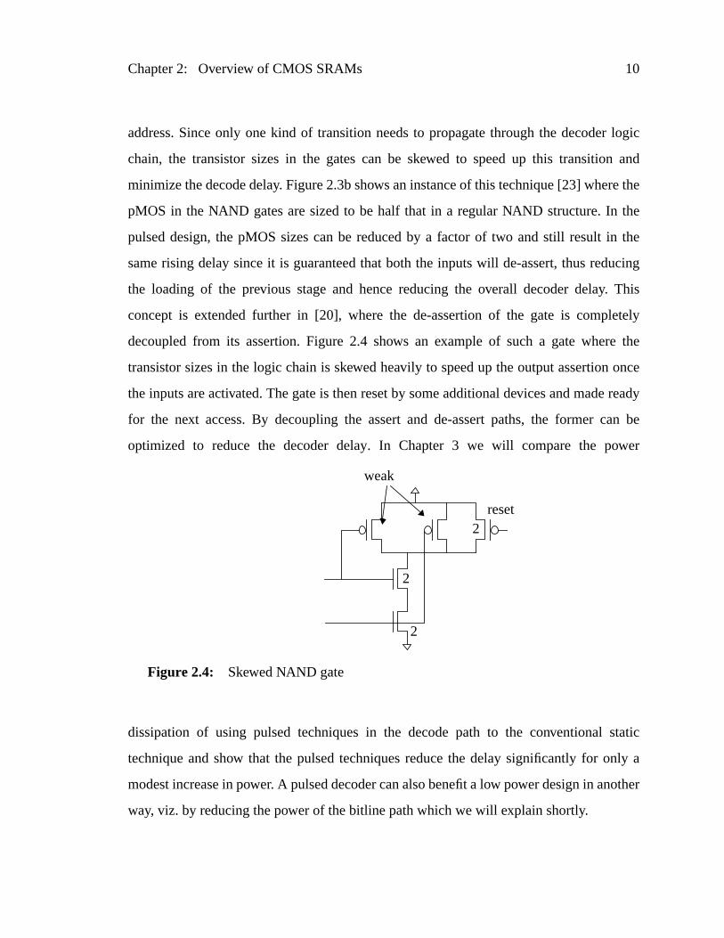
the loading of the previous stage and hence reducing the overall decoder delay
concept is extended further in [20], where the de-assertion of the gate is comp
decoupled from its assertion. Figure 2.4 shows an example of such a gate whe
transistor sizes in the logic chain is skewed heavily to speed up the output assertion
the inputs are activated. The gate is then reset by some additional devices and made
for the next access. By decoupling the assert and de-assert paths, the former c
optimized to reduce the decoder delay. In Chapter 3 we will compare the po
dissipation of using pulsed techniques in the decode path to the conventional
technique and show that the pulsed techniques reduce the delay significantly for o
modest increase in power. A pulsed decoder can also benefit a low power design in a
way, viz. by reducing the power of the bitline path which we will explain shortly.
2
2
weak
reset2
Figure 2.4: Skewed NAND gate
Chapter 2: Overview of CMOS SRAMs 11
a
wo
r to a
ther
t can
of
er of
s
or a
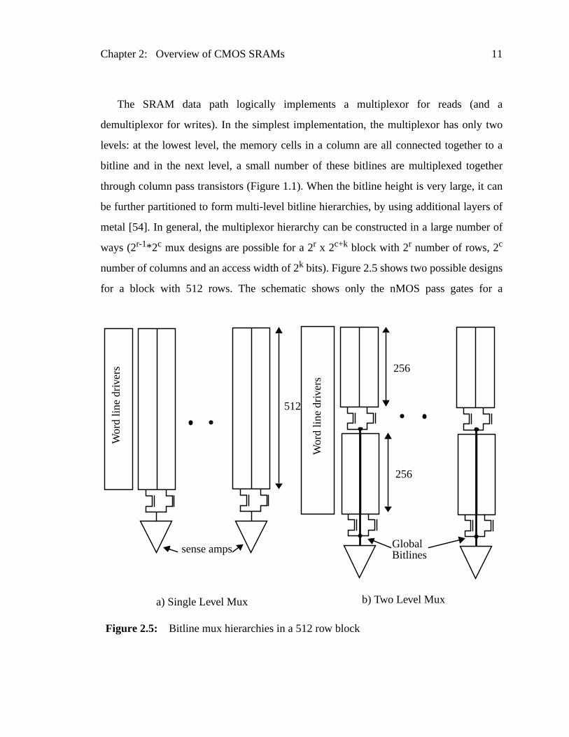
The SRAM data path logically implements a multiplexor for reads (and
demultiplexor for writes). In the simplest implementation, the multiplexor has only t
levels: at the lowest level, the memory cells in a column are all connected togethe
bitline and in the next level, a small number of these bitlines are multiplexed toge
through column pass transistors (Figure 1.1). When the bitline height is very large, i
be further partitioned to form multi-level bitline hierarchies, by using additional layers
metal [54]. In general, the multiplexor hierarchy can be constructed in a large numb
ways (2r-1*2c mux designs are possible for a 2r x 2c+k block with 2r number of rows, 2c
number of columns and an access width of 2k bits). Figure 2.5 shows two possible design
for a block with 512 rows. The schematic shows only the nMOS pass gates f
512
256
256
Wor
d lin
e dr
iver
s
Wor
d lin
e dr
iver
s
GlobalBitlines
a) Single Level Mux b) Two Level Mux
sense amps
Figure 2.5: Bitline mux hierarchies in a 512 row block
Chapter 2: Overview of CMOS SRAMs 12
uld
2.5a
h are
hich
in
larly
ll the
ring
all as
ses the
eads
g the
ines
ntrol
ting
wing
they
ype
type
gion
full
s of
sume
ferred
used
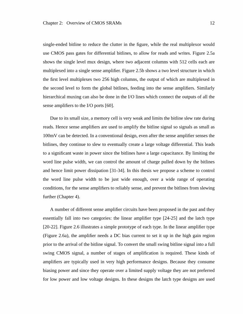
single-ended bitline to reduce the clutter in the figure, while the real multiplexor wo
use CMOS pass gates for differential bitlines, to allow for reads and writes. Figure
shows the single level mux design, where two adjacent columns with 512 cells eac
multiplexed into a single sense amplifier. Figure 2.5b shows a two level structure in w
the first level multiplexes two 256 high columns, the output of which are multiplexed
the second level to form the global bitlines, feeding into the sense amplifiers. Simi
hierarchical muxing can also be done in the I/O lines which connect the outputs of a
sense amplifiers to the I/O ports [60].
Due to its small size, a memory cell is very weak and limits the bitline slew rate du
reads. Hence sense amplifiers are used to amplify the bitline signal so signals as sm
100mV can be detected. In a conventional design, even after the sense amplifier sen
bitlines, they continue to slew to eventually create a large voltage differential. This l
to a significant waste in power since the bitlines have a large capacitance. By limitin
word line pulse width, we can control the amount of charge pulled down by the bitl
and hence limit power dissipation [31-34]. In this thesis we propose a scheme to co
the word line pulse width to be just wide enough, over a wide range of opera
conditions, for the sense amplifiers to reliably sense, and prevent the bitlines from sle
further (Chapter 4).
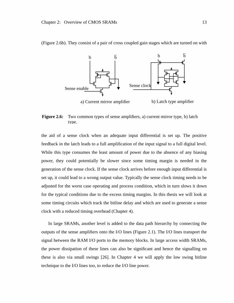
A number of different sense amplifier circuits have been proposed in the past and
essentially fall into two categories: the linear amplifier type [24-25] and the latch t
[20-22]. Figure 2.6 illustrates a simple prototype of each type. In the linear amplifier
(Figure 2.6a), the amplifier needs a DC bias current to set it up in the high gain re
prior to the arrival of the bitline signal. To convert the small swing bitline signal into a
swing CMOS signal, a number of stages of amplification is required. These kind
amplifiers are typically used in very high performance designs. Because they con
biasing power and since they operate over a limited supply voltage they are not pre
for low power and low voltage designs. In these designs the latch type designs are
Chapter 2: Overview of CMOS SRAMs 13
with
sitive
el.
iasing
the
tial is
to be
own
k at
ense
g the
rt the
Ms,
ng on
ine
(Figure 2.6b). They consist of a pair of cross coupled gain stages which are turned on
the aid of a sense clock when an adequate input differential is set up. The po
feedback in the latch leads to a full amplification of the input signal to a full digital lev
While this type consumes the least amount of power due to the absence of any b
power, they could potentially be slower since some timing margin is needed in
generation of the sense clock. If the sense clock arrives before enough input differen
set up, it could lead to a wrong output value. Typically the sense clock timing needs
adjusted for the worst case operating and process condition, which in turn slows it d
for the typical conditions due to the excess timing margins. In this thesis we will loo
some timing circuits which track the bitline delay and which are used to generate a s
clock with a reduced timing overhead (Chapter 4).
In large SRAMs, another level is added to the data path hierarchy by connectin
outputs of the sense amplifiers onto the I/O lines (Figure 2.1). The I/O lines transpo
signal between the RAM I/O ports to the memory blocks. In large access width SRA
the power dissipation of these lines can also be significant and hence the signalli
these is also via small swings [26]. In Chapter 4 we will apply the low swing bitl
technique to the I/O lines too, to reduce the I/O line power.
Sense clock
b b
Sense enable
b b
a) Current mirror amplifier b) Latch type amplifier
Figure 2.6: Two common types of sense amplifiers, a) current mirror type, b) latchtype.

Chapter 2: Overview of CMOS SRAMs 14
Chapter
level
ccess
WL
gh the
ich in
the
timal
3 Fast Low PowerDecoders
As was described in Chapter 2, a fast decoder often uses pulses rather than
signals [20-22]. These pulse mode circuits also help reduce the power of the bitline a
path [27-34]. This chapter explores the design of fast low power decoders.
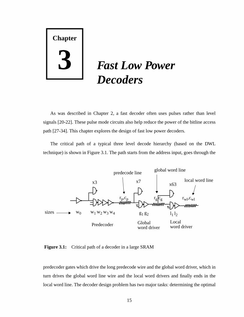
The critical path of a typical three level decode hierarchy (based on the D
technique) is shown in Figure 3.1. The path starts from the address input, goes throu
predecoder gates which drive the long predecode wire and the global word driver, wh
turn drives the global word line wire and the local word drivers and finally ends in
local word line. The decoder design problem has two major tasks: determining the op
rwl,cwlrg cgrp,cp
w0 w1 w2 w3 w4 g1 g2 l1 l2
x63x7x3
global word linepredecode line
sizes
local word line
Predecoder Globalword driver
Localword driver
Figure 3.1: Critical path of a decoder in a large SRAM
15
Chapter 3: Fast Low Power Decoders 16
the
for
has
The
s to
3.1).
p the
s will
power
y the
is to
ay is to
very
will
a valid
nnect
ions in
the
ore
ergy
e the
mple
this
elay,
circuit style and decode structure and finding the optimal sizes for the circuits and
amount of buffering at each level. The problem of optimally sizing a chain of gates
optimal delay and power is well understood [12-16]. Since the decode path also
intermediate interconnect, we will analyze the optimal sizing problem in this context.
analysis will lead to some formulae for bounding the decoder delay and allow u
evaluate some simple heuristics for doing the sizing in practical situations (Section
We will then look at various circuit techniques that have been proposed to speed u
decode path and analyze their delay and power characteristics (Section 3.2). Thi
eventually enable us to sketch the optimal decode structures to achieve fast and low
operation (Section 3.3).
3.1 Optimum Sizing and Buffering
The critical path of a typical decoder has multiple chains of gates separated b
intermediate interconnect wires. An important part of the decoder design process
determine the optimal sizes and number of stages in each of these chains. When del
be minimized, the optimum sizing criterion can be analytically derived using some
simple models for the delay of the gates and the interconnect. In this analysis we
assume that the interconnect is fixed and independent of the decoder design. This is
assumption for 2 level and 3 level decode hierarchies as the intermediate interco
serves the purpose of shipping the signals across the array. Since the array dimens
most SRAM implementations are fixed (typically about twice the area occupied by
cells), the interconnect lengths are also fixed. When the objective function is m
complicated like the energy-delay product or some weighted linear combination of en
and delay, then numerical optimization techniques have to be used to determin
optimal sizing. In practice, designers size either for minimum delay, or use some si
heuristics to back off from a minimum delay solution so as to reduce energy. In
section we will explore various sizing techniques and explain their impact on the d
Chapter 3: Fast Low Power Decoders 17
g a
cal
t
and
ully
unit.
is
arasitic
r
e
f its
energy and area of the decoder.
We introduce our notations by first reviewing the classic problem of optimally sizin
chain of inverters to drive a fixed output load. We will adopt terminology from the Logi
Effort work of Sutherland and Sproull [35].
3.1.1 Review of Optimum Inverter Chain Design
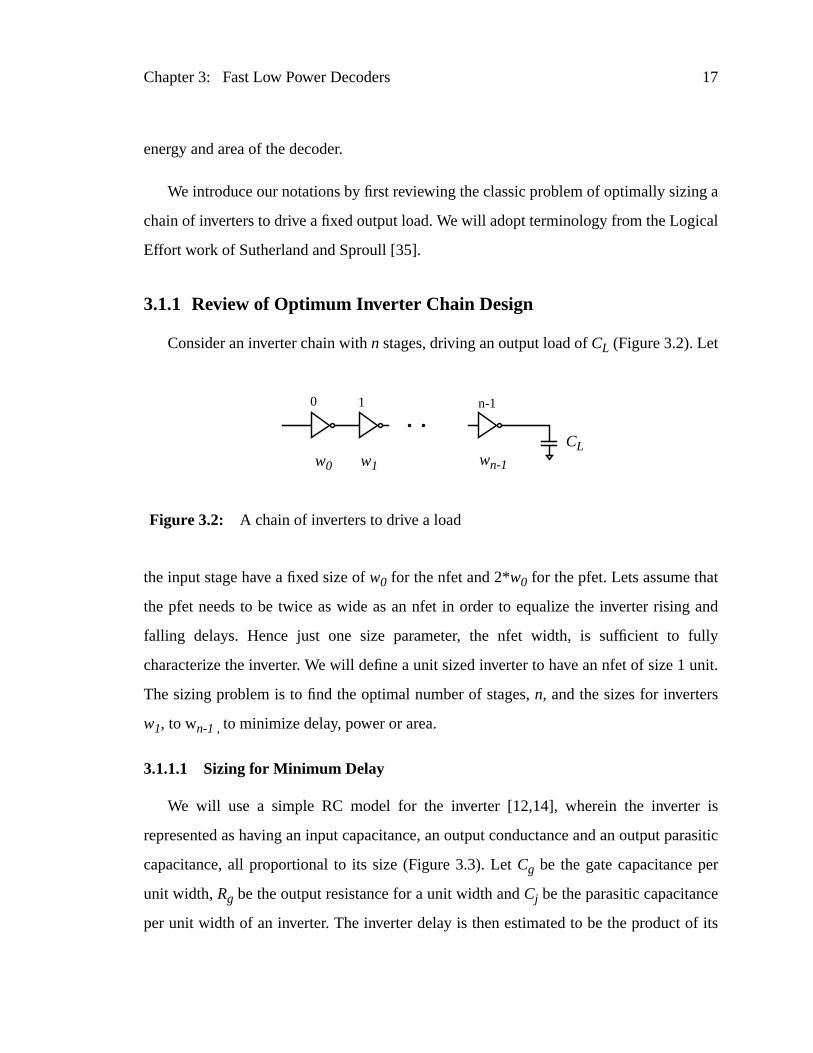
Consider an inverter chain withn stages, driving an output load ofCL (Figure 3.2). Let
the input stage have a fixed size ofw0 for the nfet and 2*w0 for the pfet. Lets assume tha
the pfet needs to be twice as wide as an nfet in order to equalize the inverter rising
falling delays. Hence just one size parameter, the nfet width, is sufficient to f
characterize the inverter. We will define a unit sized inverter to have an nfet of size 1
The sizing problem is to find the optimal number of stages,n, and the sizes for inverters
w1, to wn-1 ,to minimize delay, power or area.
3.1.1.1 Sizing for Minimum Delay
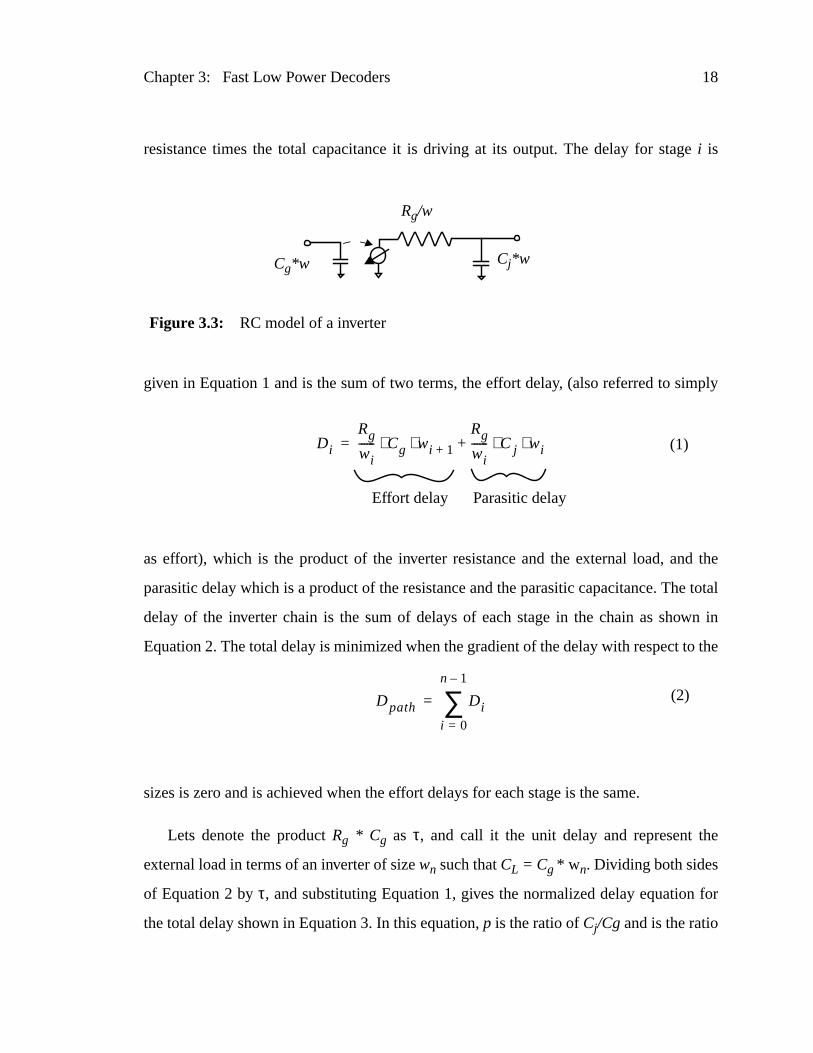
We will use a simple RC model for the inverter [12,14], wherein the inverter
represented as having an input capacitance, an output conductance and an output p
capacitance, all proportional to its size (Figure 3.3). LetCg be the gate capacitance pe
unit width,Rg be the output resistance for a unit width andCj be the parasitic capacitanc
per unit width of an inverter. The inverter delay is then estimated to be the product o
w0
0 1 n-1
w1 wn-1
CL
Figure 3.2: A chain of inverters to drive a load
Chapter 3: Fast Low Power Decoders 18
e
ply
d the
e total
wn in
o the
e
for
resistance times the total capacitance it is driving at its output. The delay for stagi is
given in Equation 1 and is the sum of two terms, the effort delay, (also referred to sim
as effort), which is the product of the inverter resistance and the external load, an
parasitic delay which is a product of the resistance and the parasitic capacitance. Th
delay of the inverter chain is the sum of delays of each stage in the chain as sho
Equation 2. The total delay is minimized when the gradient of the delay with respect t
sizes is zero and is achieved when the effort delays for each stage is the same.
Lets denote the productRg * Cg as τ, and call it the unit delay and represent th
external load in terms of an inverter of sizewn such thatCL = Cg * wn. Dividing both sides
of Equation 2 byτ, and substituting Equation 1, gives the normalized delay equation
the total delay shown in Equation 3. In this equation,p is the ratio ofCj/Cgand is the ratio
Rg/w
Cj*wCg*w
Figure 3.3: RC model of a inverter
Di
Rg
wi------ Cg wi 1+⋅ ⋅
Rg
wi------ Cj wi⋅ ⋅+= (1)
Effort delay Parasitic delay
Dpath Dii 0=
n 1–
∑= (2)
Chapter 3: Fast Low Power Decoders 19
ce of
the
lear.
as
nd is
ns 4
t to
gives
itic
by
to
,
ery
of the drain junction capacitance of the output of the inverter with the gate capacitan
the inputs and is approximately independent of the inverter size. We will call
normalized effort delay of a stage as its stage effort, or simply effort if the context is c
For minimum delay, all the stage efforts are equal to each other and we denote themf in
Equation 4. The product of all the stage efforts is a constant called the path effort a
the ratio of the output load and the size of the input driver (5). With the aid of Equatio
and 5 total delay can be expressed as in (6). Differentiating Equation 6 with respecf
and setting the derivative to zero results in Equation 7. The solution to Equation 7
the optimum stage effort which will minimize the total delay [14]. When the paras
delay p is zero, thenf = e is the optimum solution and is the classic result derived
Jaeger in [12]. In generalp is not zero and Equation 7 needs to be solved numerically
obtain the optimal stage effort. For the base 0.25µm technology described in Appendix C
p = 1.33 and sof = 3.84 is the optimum effort per stage. In practice the delay is not v
sensitive to the stage effort so to minimize power larger stage efforts are preferred.
Dpath τ⁄wi 1+
wi------------- p+
i 0=
n 1–
∑= (3)
w1
w0------
w2
w1------=
wn
wn 1–--------------= f= (4)
fn wn
w0------
CL Cg⁄w0
------------------= =
Dpath τ⁄ f p+( ) wn w0⁄( ) f( )ln⁄ln⋅=
(5)
(6)
f( )ln 1– pf---– 0= (7)
Chapter 3: Fast Low Power Decoders 20
ower
ulta-
due to
ower
nt
output
er of
mic
to the
future
urrent
to
as the
tran-
age,
the
ome
3.1.1.2 Sizing for Minimum Power
The power dissipation in an inverter consists of three components, the dynamic p
to switch the load and parasitic capacitance, the short circuit power due to the sim
neous currents in the pfet and nfet during a signal transition and the leakage power
the subthreshold conduction in the fets which are supposed to be off. The dynamic p
dissipation during one switching cycle in stagei of Figure 3.2 is the power to switch the
gate load of stagei+1 and self loading of stagei and is given in Equation 8, withVdd rep-
resenting the supply voltage andf, the operating frequency. The short circuit curre
through the inverter depends on the edge rate of the input signal and the size of the
load being driven [36]. Cherkauer and Friedman in [16] estimate the short circuit pow
stagei in the chain to be proportional to the total capacitive load, just as the dyna
power is. The subthreshold leakage current has been traditionally very small due
high threshold voltages of the fets, but they are expected to become important in the
as the thresholds are scaled down in tandem with the supply voltage. The leakage c
of stagei is proportional to the sizewi. Since all the three components are proportional
the size of the stage, the total normalized power dissipation can be simply expressed
sum of the inverter sizes as in Equation 9. Power is reduced when the total width of
sistors in the chain is minimized. The minimum power solution has exactly one st
which is the input driver directly driving the load and is not very interesting due to
large delays involved. We will next look at sizing strategies to reduce power with s
delay constraint.
PDY i, Cg wi 1+⋅ Cj wi⋅+( ) Vdd2
frequency⋅ ⋅= (8)
P wii 0=
n
∑= (9)

Chapter 3: Fast Low Power Decoders 21
f the
blem
ain
n the
same
the
miz-
bout
ffort
mini-
n be
delay
nimum
pti-
ore
erter
ath at
Logic
anch-
s
e nfets
3.1.1.3 Sizing for Minimum Delay and Power
In practical designs there is usually an upper bound on the delay specification o
chain and the power needs to be minimized subject to this constraint. The sizing pro
in this case can only be solved numerically via some optimization program [15]. The m
feature of the optimum solution is that the stage efforts increase as one goes dow
chain.
A simpler approach to the sizing problem is to design each stage to have the
stage effort, but instead find the stage effort which minimizes energy, while meeting
delay constraint. Choi and Lee in [15] investigate this approach in the context of mini
ing the power-delay product and they find that the solution requires stage efforts of a
6.5 and is within a few percent of the globally optimal solution. The larger stage e
leads to smaller number of stages as well as lower power solution compared to the
mum delay design. Further improvements in delay at minimal expense of power ca
obtained by observing that the stages in the beginning of the chain provide as much
as the latter ones, but consume less power, and so one can have stage efforts for mi
delay in the initial stages and larger efforts for the final stages, mirroring the globally o
mal solution [37].
With this background on sizing gates, we will next turn our attention to the c
problem of this section, viz., how to size a decoder optimally.
3.1.2 Sizing the Decoder
The three key features of the decode path which distinguishes it from a simple inv
chain is the presence of logic gates other than inverters, branching of the signal p
some of the intermediate nodes, and the presence of interconnect inside the path.
gates and branching are easily handled by using the concept of logical effort and br
ing effort introduced in [35].
A complex gate like an n-input NAND gate hasn nfets in series, which degrades it
speed compared to an inverter. To obtain the same drive strength as the inverter, th
Chapter 3: Fast Low Power Decoders 22
ND
gth.
h is
nnel
ious
ion of
ut to a
ut to
ord
factor
e and
and
is
effort
e five
have to be sizedn times bigger, causing the input capacitance for each of the NA
inputs to be(n+2)/3 times bigger than that of an inverter having the same drive stren
This extra factor is called the logical effort of the gate. The total logical effort of the pat
the product of logical efforts of each gate in the path. We note here that for short cha
fets, the actual logical effort of complex gates is lower than that predicted by the prev
simple formula since the fets are velocity saturated, and the output current degradat
a stack of fets will be lesser than in the long channel case.
In the decode path, the signal at some of the intermediate nodes is branched o
number of identical stages, e.g. the global word line signal in Figure 3.1 is branched o
a number (be) of local word driver stages. Thus any change in sizes of the local w
driver stage is has an impact on the global word line signal which is enhanced by the
of be. The amount of branching at each node is called the branching effort of the nod
the total branching effort of the path is the product of all the node branching efforts.
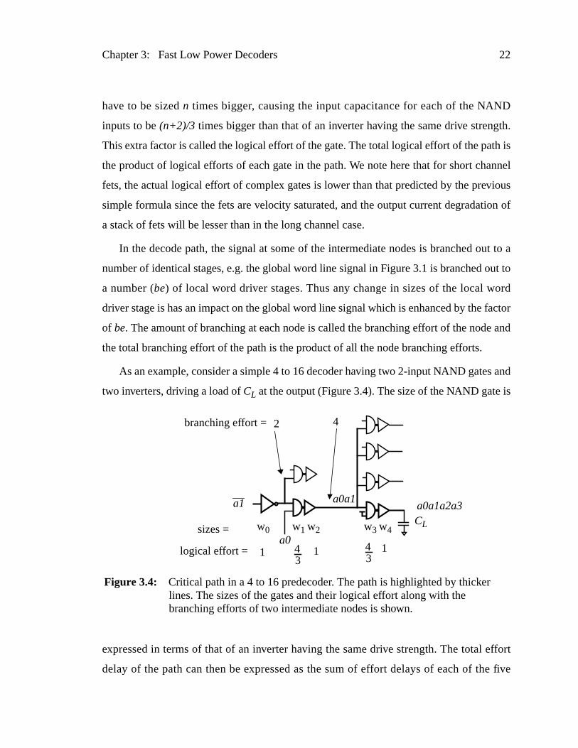
As an example, consider a simple 4 to 16 decoder having two 2-input NAND gates
two inverters, driving a load ofCL at the output (Figure 3.4). The size of the NAND gate
expressed in terms of that of an inverter having the same drive strength. The total
delay of the path can then be expressed as the sum of effort delays of each of th
w1 w2 w3 w4
42
CLw0
1 43
43
1 1
branching effort =
sizes =
logical effort =
a1
a0
a0a1a0a1a2a3
Figure 3.4: Critical path in a 4 to 16 predecoder. The path is highlighted by thickerlines. The sizes of the gates and their logical effort along with thebranching efforts of two intermediate nodes is shown.
Chapter 3: Fast Low Power Decoders 23
ffort
of
, and
rt is
he
s.
. If
rion
total
nd
oreti-
the
e the
stages in the critical path and is given as in Equation 10. To minimize this delay, the e
of each stage needs to be the same (f), and can be obtained by relating it to the product
the stage efforts as in Equation 11. Since each NAND gate has a logical effort of 4/3
two of the intermediate nodes have branching efforts of 2 and 4, the total path effo
enhanced by a factor of 128/9 in Equation 11.
In general for a r to 2r decode, the total branching effort of the critical path from t
input or its complement to the output is 2r-1 since each input selects half of all the output
The total logical effort of the path is the effort needed to build an r-input AND function
the wire delays within the decoder are insignificant then the optimal sizing crite
remains the same as in the case of the inverter chain. The only difference is that the
path effort gets multiplied by the total logical effort and the total branching effort a
hence affects the optimal number of stages in the path as shown in Equation 12. The
cally, the optimum stage effort differs slightly from that for a inverter chain (since
parasitics of logic gates will be more than that of an inverter in general), but in practic
same stage effort of about 4 suffices to give a good solution.
D
43--- w1 2⋅ ⋅
w0---------------------
w2
w1------
43--- w3 4⋅ ⋅
w2---------------------
w4
w3------
CL
w4------- parasitics+ + + + += (10)
(11)
Stage efforts for stage 0 stage 1 stage 2 stage 4
f5
43---
22 4 CL⋅ ⋅ ⋅
w0--------------------------------------=Total path effort equals
fn outputLoad 2
r 1–LogicalEffort r input– AND–( )⋅ ⋅
w0----------------------------------------------------------------------------------------------------------------------------------------= (12)

Chapter 3: Fast Low Power Decoders 24
inter-
rter
paci-
next
more
rcon-
in the
edi-
s for
num-
long
f
wo
y is
The final distinguishing feature of the decode path, the presence of intermediate
connect, can lead to an optimal sizing criterion which is different then that for the inve
chain. Ohbayashi, et. al. in [38] have shown that when the interconnect is purely ca
tive, the optimal stage efforts for minimum delay reduces along the chain. In the
subsections we will derive this result as a special case of treating the interconnect
generally as having both resistance and capacitance. We will show that when the inte
nect has both R and C, the optimal stage efforts for all the stages is still the same as
inverter chain case, but this might require non integral number of stages in the interm
ate sub chains, which is not physically realizable. We will also provide expression
optimal efforts when the intermediate chains are forced to have some fixed integral
ber of stages. We will finally consider sizing strategies for reducing power and area a
with the delay.
3.1.2.1 Sizing an Inverter Chain with Fixed Intermediate Interconnect for
Minimum Delay
Without loss of generality, consider an inverter chain driving a fixed loadCL, and hav-
ing two sub chains separated by interconnect having a resistance and capacitance oRwire
andCwire respectively. To simplify the notations in the equations we will introduce t
new normalized variablesR andC which are obtained asR = Rwire/Rg andC = Cwire/Cg.
This will make all our delays come out in units ofτ (= Rg*Cg). Again we will assume that
the input inverter has a fixed size ofw0 (Figure 3.5). The first subchain hasn+1 stages,
with sizesw0 to wn and the second subchain hask stages with sizesx1 to xk. The goal is to
find the number of stagesn, k and the sizes of each stage such that the total dela
minimized.
w0
0 1 n
w1 wn
CL
R
C/2C/2
1 k
x1 xk
Figure 3.5: Buffer chain with intermediate interconnect
Chapter 3: Fast Low Power Decoders 25
e
nd is
elay of
with
re sat-
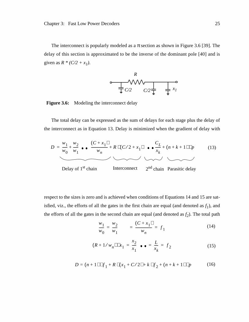
The interconnect is popularly modeled as aπ section as shown in Figure 3.6 [39]. Th
delay of this section is approximated to be the inverse of the dominant pole [40] a
given asR * (C/2 + x1).
The total delay can be expressed as the sum of delays for each stage plus the d
the interconnect as in Equation 13. Delay is minimized when the gradient of delay
respect to the sizes is zero and is achieved when conditions of Equations 14 and 15 a
isfied, viz., the efforts of all the gates in the first chain are equal (and denoted asf1), and
the efforts of all the gates in the second chain are equal (and denoted asf2). The total path
R
C/2C/2 x1
Figure 3.6: Modeling the interconnect delay
Dw1
w0------
w2
w1------+=
C x1+( )wn
-------------------- R C 2⁄ x1+( )⋅+CL
xk------- n k 1+ +( ) p⋅+ (13)
Delay of 1st chain Interconnect 2nd chain Parasitic delay
w1
w0------
w2
w1------=
C x1+( )wn
--------------------= f 1=
R 1 wn⁄+( ) x1⋅x2
x1-----= L
xk-----= f 2=
(14)
(15)
D n 1+( ) f 1⋅ R x1 C 2⁄+( )⋅ k+ f 2⋅+= n k 1+ +( ) p⋅+ (16)
Chapter 3: Fast Low Power Decoders 26
ua-
en
ain is
cond
ound
in
is
nter-
more
nce
istance
opti-
delay for minimum delay can than be rewritten in terms of the optimal efforts as in Eq
tion 16. By inspecting Equations 14 and 15, we can also obtain a relationship betwef1
andf2 as in Equation 17. From this we can deduce that ifR=0, f2 < f1, and is the case dis-
cussed by [38]. In this scenario, for minimum delay the stage effort for the second ch
less than the stage effort of the first chain. Similarly, whenC = 0, f1 < f2, the exact dual
occurs, i.e., the stage effort of the first chain is less than the stage effort of the se
chain.
Analogous to the single chain case, the minimum delay in Equation 16 can be f
by finding the optimum values forf1, f2, n and kand the detailed derivation is presented
Appendix A. The main result of this exercise is that for minimum delay whenR andC are
non-zero,f1 = f2 = f , andf is the solution of Equation 7, i.e., the same sizing rule which
used for the simple inverter chain, is also the optimal for the chain with intermediate i
connect. The appendix also shows that this result holds true even for chains with
than one intermediate interconnect stage.
An interesting corollary can be observed by substitutingf1 = f2 = f in Equation 17 to
obtain the following necessary condition for optimum, viz., the product of wire resista
times the down stream gate capacitance is the same as the product of the driver res
times the wire capacitance (18). The same condition also turns up in the solution of
mal repeater insertion in a long resistive wire [39].
f 1
f 2------
C x1+( ) wn⁄R 1 wn⁄+( ) x1⋅
--------------------------------------= (17)
C wn⁄ R x1⋅= (18)
Chapter 3: Fast Low Power Decoders 27
r too
0 as
ded
qua-
ificant
treat
s final
as its
tions
ields
input
rcon-
The appendix also derives analytical expressions for optimumn andk and they are
reproduced in Equations 19 and 20. If the interconnect delay is either too large o
small compared to the inverter delay, then we can simplify Equations 19 and 2
follows:
A. RC/2 >> 2f
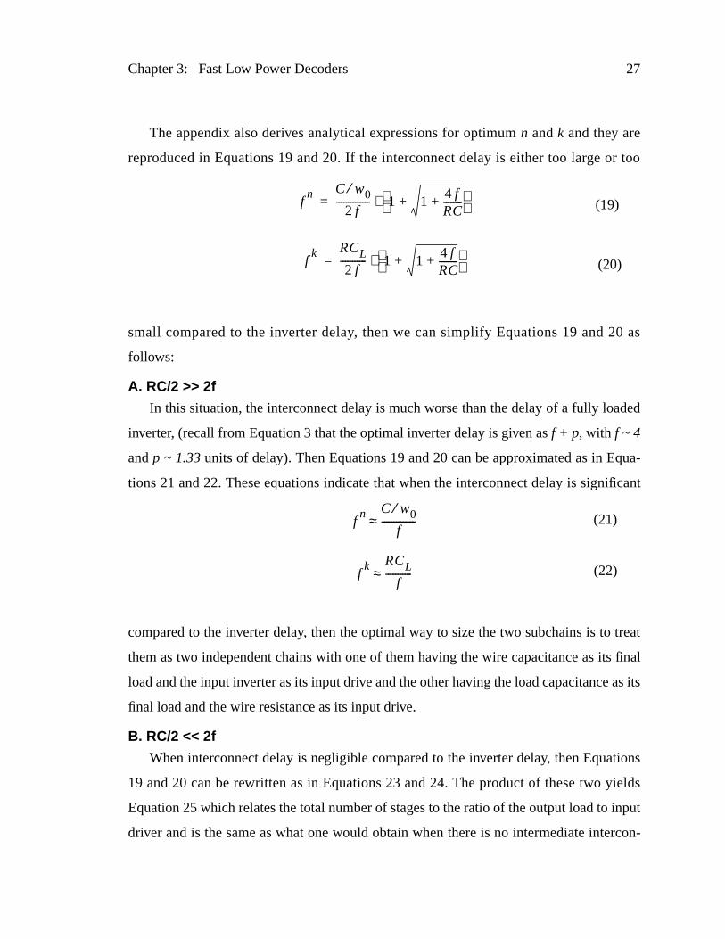
In this situation, the interconnect delay is much worse than the delay of a fully loa
inverter, (recall from Equation 3 that the optimal inverter delay is given asf + p, with f ~ 4
andp ~ 1.33units of delay). Then Equations 19 and 20 can be approximated as in E
tions 21 and 22. These equations indicate that when the interconnect delay is sign
compared to the inverter delay, then the optimal way to size the two subchains is to
them as two independent chains with one of them having the wire capacitance as it
load and the input inverter as its input drive and the other having the load capacitance
final load and the wire resistance as its input drive.
B. RC/2 << 2f
When interconnect delay is negligible compared to the inverter delay, then Equa
19 and 20 can be rewritten as in Equations 23 and 24. The product of these two y
Equation 25 which relates the total number of stages to the ratio of the output load to
driver and is the same as what one would obtain when there is no intermediate inte
fn C w0⁄
2 f-------------- 1 1 4 f
RC--------++
⋅=
fk RCL
2 f----------- 1 1 4 f
RC--------++
⋅=
(19)
(20)
fn C w0⁄
f--------------≈
fk RCL
f-----------≈
(21)
(22)
Chapter 3: Fast Low Power Decoders 28
nly its
stance
e the
mini-
dual
nce is
nect
ense.
ical
rarchy
drive
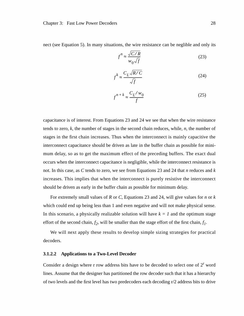
nect (see Equation 5). In many situations, the wire resistance can be neglible and o
capacitance is of interest. From Equations 23 and 24 we see that when the wire resi
tends to zero,k, the number of stages in the second chain reduces, while,n, the number of
stages in the first chain increases. Thus when the interconnect is mainly capacitiv
interconnect capacitance should be driven as late in the buffer chain as possible for
mum delay, so as to get the maximum effect of the preceding buffers. The exact
occurs when the interconnect capacitance is negligible, while the interconnect resista
not. In this case, asC tends to zero, we see from Equations 23 and 24 thatn reduces andk
increases. This implies that when the interconnect is purely resistive the intercon
should be driven as early in the buffer chain as possible for minimum delay.
For extremely small values ofR or C, Equations 23 and 24, will give values forn or k
which could end up being less than 1 and even negative and will not make physical s
In this scenario, a physically realizable solution will havek = 1 and the optimum stage
effort of the second chain,f2, will be smaller than the stage effort of the first chain,f1.
We will next apply these results to develop simple sizing strategies for pract
decoders.
3.1.2.2 Applications to a Two-Level Decoder
Consider a design where r row address bits have to be decoded to select one of 2r word
lines. Assume that the designer has partitioned the row decoder such that it has a hie
of two levels and the first level has two predecoders each decoding r/2 address bits to
fn C R⁄
w0 f----------------≈
fk CL R C⁄
f-----------------------≈
fn k+ CL w0⁄
f-----------------≈
(23)
(24)
(25)
Chapter 3: Fast Low Power Decoders 29
on
erate
gure
rter
ogical
vers
r
,
tical
al
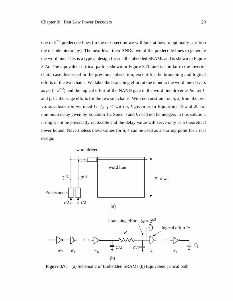
one of 2r/2 predecode lines (in the next section we will look at how to optimally partiti
the decode hierarchy). The next level then ANDs two of the predecode lines to gen
the word line. This is a typical design for small embedded SRAMs and is shown in Fi
3.7a. The equivalent critical path is shown in Figure 3.7b and is similar to the inve
chain case discussed in the previous subsection, except for the branching and l
efforts of the two chains. We label the branching effort at the input to the word line dri
asbe (= 2r/2) and the logical effort of the NAND gate in the word line driver asle. Let f1
andf2 be the stage efforts for the two sub chains. With no constraint onn, k, from the pre-
vious subsection we needf1=f 2=f~4 with n, k given as in Equations 19 and 20 fo
minimum delay given by Equation 16. Sincen andk need not be integers in this solution
it might not be physically realizable and the delay value will serve only as a theore
lower bound. Nevertheless these values forn, k can be used as a starting point for a re
design.
2r rows
word line
word driver
Predecoders
w0 w1 wn
CL
R
C/2C/2x1 xk
be= 2r/2branching effort=
Figure 3.7: (a) Schematic of Embedded SRAMs (b) Equivalent critical path
logical effortle
r/2 r/2
2r/2 2r/2
1
(a)
(b)

Chapter 3: Fast Low Power Decoders 30
e
. The
put
c-
hain
irst
The
the
he
are a
rd
Since the problem of finding a solution with integern stages in the predecoder is th
same as that for a simple buffer chain (see Equation 12), we will not discuss it here
optimum number of integral stages in the word driver can be obtained by roundingk to the
nearest even integer if the word driver implements the AND logical function of its in
i.e. for k in 2i to 2i+1, roundk to be2i and fork between2i+1 to 2i+2, roundk to 2i+2.
Similarly, roundk to the nearest odd integer if the word driver implements the AND fun
tion of the complement of the inputs. Since the number of stages in the word driver c
has now been constrained to be an integer, the optimal effort in this sub chain (f2) need no
longer be equal tof(~4). We present three alternatives to recompute this effort: the f
(labeled as OPT) sets up an equation for delay in terms off2 and minimizes it to obtain the
optimal solution for the specific integer number of stages in the word driver chain.
remaining two are heuristics which we will describe shortly.
We will next describe the approach to compute the optimum stage efforts with
number of stages in the word driver chain constrained to be an even integer (ik), close to
the value ofk obtained previously. Applying the condition for minimum delay, that t
stage efforts in each of the sub chains be equal, we get Equations 26 and 27, which
modification of Equations 14 and 15 and include the effects of the logical (le) and branch-
ing efforts (be). The effects ofle andbecause the gate loading of the input of the wo
driver (x1) to be enhanced by a factor ofbe * le. Substituting forx1 = CL/f2ik and eliminat-
(26)
(27)
w1
w0------
w2
w1------=
C be le x1⋅ ⋅+
wn-----------------------------------= f=
R1
wn------+
be le x1⋅ ⋅ ⋅x2
x1-----= f 2=
Chapter 3: Fast Low Power Decoders 31
it has
ua-
ding
rfor-
that
efore
t 4
. But
bit
small
ich
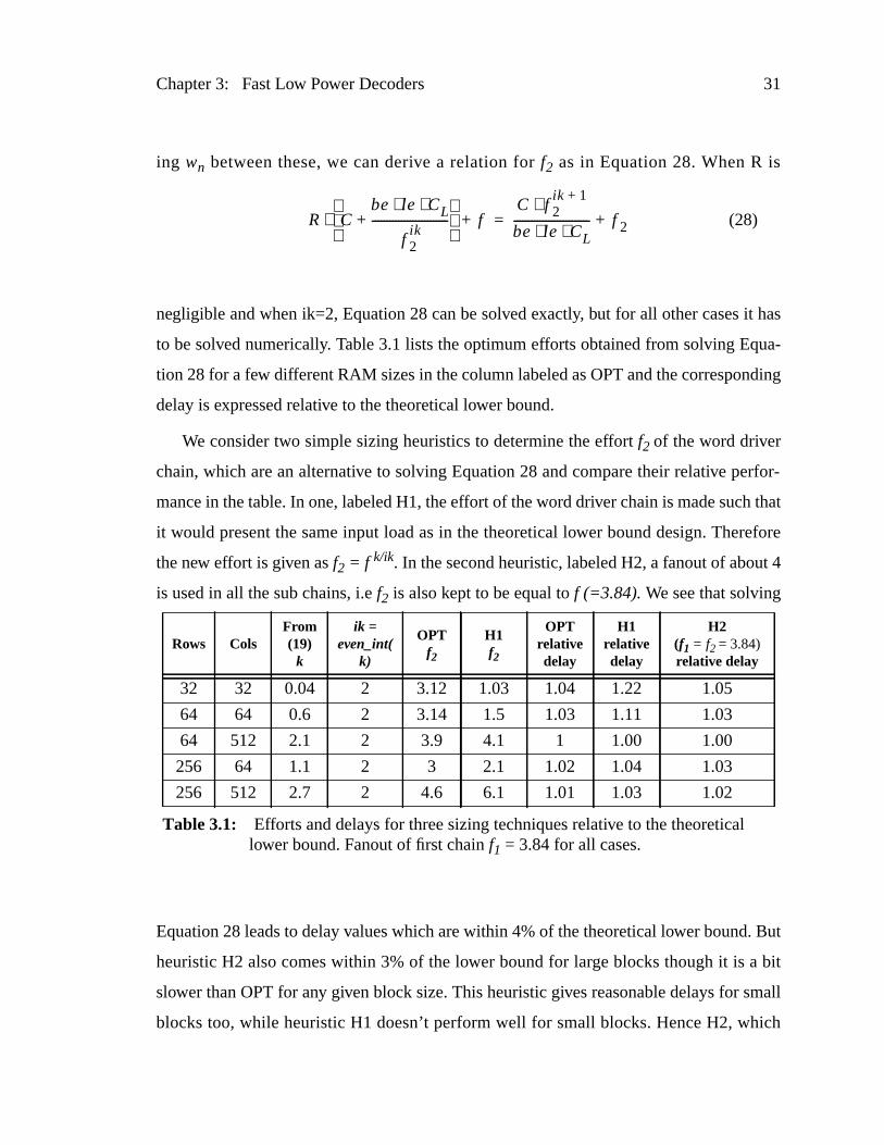
ing wn between these, we can derive a relation forf2 as in Equation 28. When R is
negligible and when ik=2, Equation 28 can be solved exactly, but for all other cases
to be solved numerically. Table 3.1 lists the optimum efforts obtained from solving Eq
tion 28 for a few different RAM sizes in the column labeled as OPT and the correspon
delay is expressed relative to the theoretical lower bound.
We consider two simple sizing heuristics to determine the effortf2 of the word driver
chain, which are an alternative to solving Equation 28 and compare their relative pe
mance in the table. In one, labeled H1, the effort of the word driver chain is made such
it would present the same input load as in the theoretical lower bound design. Ther
the new effort is given asf2 = f k/ik. In the second heuristic, labeled H2, a fanout of abou
is used in all the sub chains, i.ef2 is also kept to be equal tof (=3.84).We see that solving
Equation 28 leads to delay values which are within 4% of the theoretical lower bound
heuristic H2 also comes within 3% of the lower bound for large blocks though it is a
slower than OPT for any given block size. This heuristic gives reasonable delays for
blocks too, while heuristic H1 doesn’t perform well for small blocks. Hence H2, wh
Rows ColsFrom(19)
k
ik =even_int(
k)
OPTf2
H1f2
OPTrelativedelay
H1relativedelay
H2(f1 = f2 = 3.84)relative delay
32 32 0.04 2 3.12 1.03 1.04 1.22 1.05
64 64 0.6 2 3.14 1.5 1.03 1.11 1.03
64 512 2.1 2 3.9 4.1 1 1.00 1.00
256 64 1.1 2 3 2.1 1.02 1.04 1.03
256 512 2.7 2 4.6 6.1 1.01 1.03 1.02
Table 3.1: Efforts and delays for three sizing techniques relative to the theoreticallower bound. Fanout of first chainf1 = 3.84 for all cases.
R Cbe le CL⋅ ⋅
f 2ik
--------------------------+
⋅ f+C f 2
ik 1+⋅be le CL⋅ ⋅-------------------------- f 2+= (28)
Chapter 3: Fast Low Power Decoders 32
for 2
onal
ided
word
unaf-
om
uses a simple fanout of 4 sizing in the entire path forms an effective sizing strategy
level decode paths.
Large SRAMs typically use the Divided Word Line architecture which uses an additi
level of decoding, and so we next look at sizing strategies for three-level decoders.
3.1.2.3 Application to a Three-Level Decoder
Figure 3.8 depicts the critical path for a typical decoder implemented using the Div
Word Line architecture. The path has three subchains, the predecode, the global
driver and the local word driver chains. Let the number of stages in these bem, n and kand
the stage efforts bef1, f2 andf3 respectively. Letbeg andbel be the branching efforts as the
input to the global and local word drivers and letle be the logical effort of the input NAND
gate of these drivers. We will assume that the lengths of the global word lines are
fected by the sizes in the local word driver chain, to simplify the analysis. Again fr
Appendix A, if there is no constraint on the number of stages (i.e.m, n and kcan be any
real numbers), then the lower bound for delay is achieved whenf1=f2=f3=f ~ 4 and the
R2 C2R1,C1
w0 v1 w1 wn x1 xkvmL
beg bel
Figure 3.8: Critical path for a 3 level decoder
Chapter 3: Fast Low Power Decoders 33
ng off
ter-
ree
ing a
ber-
two
theo-
bal
his is
d are
e is
r
delay
nce
word
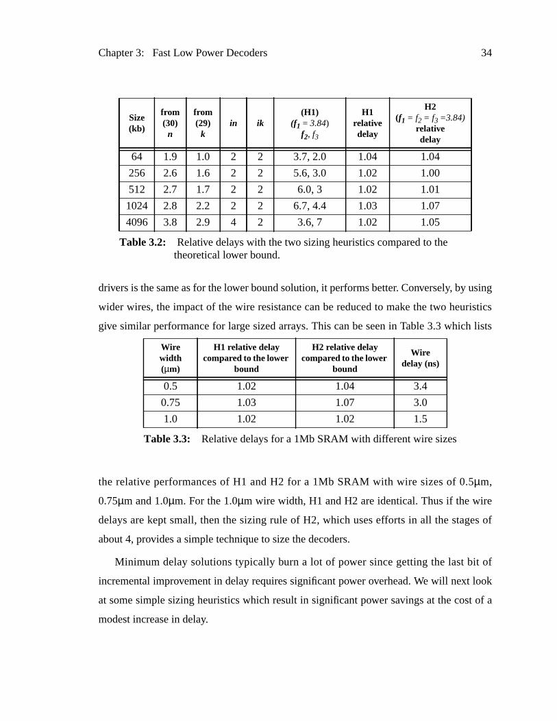
number of stages in these subchains is given by Equations 29, 30 and 31. By roundi
n andk to the nearest integersin andik as discussed in the two level case, one can de
mine the optimum efforts for a real implementation. Similar to the two-level case, th
alternatives exist: solving for exact values forf2 and f3 with these integral number of
stages or use either of the two heuristics H1 or H2. The former approach of formulat
pair of equations akin to Equation 28 and solving them simultaneously is very cum
some and we will not do that here. We will instead evaluate the performance of the
heuristics H1 and H2 discussed in the previous subsection and compare them to the
retical lower bound.
Under H1,f2 andf3 are determined such that the input loading of the local and glo
word driver chains are kept the same as in the theoretical lower bound case. T
achieved by makingf2 = fn/in andf3 = fk/ik. Under H2,f2 andf3 are kept equal tof (~4).
The relative delays of both these heuristics compared to the theoretical lower boun
shown in Table 3.2 for various SRAM sizes. The number of cells on the local word lin
128 for this table and we assume a 0.25µm technology (Appendix C). We observe that fo
large sizes, heuristic H1 performs better than H2. The main reason is that the wire
due to the input loading of the word drivers in conjunction with the wire resista
becomes important for these sizes. Since H1 ensures that the input loading of the
fk R2 L bl g⋅ ⋅ ⋅
2 f------------------------------- 1 1 4 f
R2 C2⋅-----------------++
⋅=
fn
bg gC2
C1------
1 1 4 fR2 C2⋅-----------------++
4 fR1 C1⋅----------------- 1+ 1–
----------------------------------------------⋅ ⋅ ⋅=
fm C w0⁄
2 f-------------- 1 1 4 f
R1 C1⋅-----------------++
⋅=
(29)
(30)
(31)
Chapter 3: Fast Low Power Decoders 34
using
istics
lists
e
es of
of
look
t of a
drivers is the same as for the lower bound solution, it performs better. Conversely, by
wider wires, the impact of the wire resistance can be reduced to make the two heur
give similar performance for large sized arrays. This can be seen in Table 3.3 which
the relative performances of H1 and H2 for a 1Mb SRAM with wire sizes of 0.5µm,
0.75µm and 1.0µm. For the 1.0µm wire width, H1 and H2 are identical. Thus if the wir
delays are kept small, then the sizing rule of H2, which uses efforts in all the stag
about 4, provides a simple technique to size the decoders.
Minimum delay solutions typically burn a lot of power since getting the last bit
incremental improvement in delay requires significant power overhead. We will next
at some simple sizing heuristics which result in significant power savings at the cos
modest increase in delay.
Size(kb)
from(30)n
from(29)
kin ik
(H1)(f1 = 3.84)
f2, f3
H1relativedelay
H2(f1 = f2 = f3 =3.84)
relativedelay
64 1.9 1.0 2 2 3.7, 2.0 1.04 1.04
256 2.6 1.6 2 2 5.6, 3.0 1.02 1.00
512 2.7 1.7 2 2 6.0, 3 1.02 1.01
1024 2.8 2.2 2 2 6.7, 4.4 1.03 1.07
4096 3.8 2.9 4 2 3.6, 7 1.02 1.05
Table 3.2: Relative delays with the two sizing heuristics compared to thetheoretical lower bound.
Wirewidth(µm)
H1 relative delaycompared to the lower
bound
H2 relative delaycompared to the lower
bound
Wiredelay (ns)
0.5 1.02 1.04 3.4
0.75 1.03 1.07 3.0
1.0 1.02 1.02 1.5
Table 3.3: Relative delays for a 1Mb SRAM with different wire sizes

Chapter 3: Fast Low Power Decoders 35
itch-
es, as
le 3.4
ents
ing
tances
global
CG),
tran-
oder
Rg)
of the
e to
3.1.2.4 Sizing for Fast Low Power Operation
The main component of power loss in a decoder is the dynamic power lost in sw
ing the large interconnect capacitances in the predecode, block select and word lin
well as the gate and junction capacitances in the logic gates of the decode chain. Tab
provides a detailed breakdown of the relative contribution from the different compon
to the total switching capacitance for two different SRAM sizes. The total switch
capacitance is the sum of the interconnect capacitances (CI), the transistor capaci
internal to the predecoders (CP), the mosfet gate capacitance of the input gate of the
word drivers (CW1), the transistor capacitances internal to the global word drivers (
the mosfet gate capacitance of the input gate of the local word drivers (CX1) and the
sistor capacitances internal to the local word driver (CL).
Table 3.5 shows the relative breakdown of the total delay amongst the predec
(DP), the predecode wire (DRp), the global word driver (DG), the global word line (D
and the local word driver (DL).
The two key features to note from these tables are that the input gate capacitance
two word drivers contribute a significant fraction to the total switching capacitance du
SizeInterconne
ct(CI)
PredecodeInternal
(CP)
Input ofGlobalWordDriver(CW1)
GlobalWordDriver
Internal(CG)
Input ofLocalWordDriver(CX1)
LocalWordDriver
Internal(CL)
16kb 11 20 20 10 30 7
1Mb 36 23 21 6 12.5 1.5
Table 3.4: Relative power of various components of the decode path in%
SizePredecode
(DP)Predecode
Wire (DRp)Global WordDriver (DG)
Global WordLine (DRg)
Local WordDriver (DL)
16kb 56 2 26 1 15
1Mb 44 15.5 17.5 5 18
Table 3.5: Relative delay of various components of the decode path under H1 in %
Chapter 3: Fast Low Power Decoders 36
ignif-
ivers
y also
, by
rectly
es, we
zes.
e the
se a
ord
loads
e fol-
y this
lay
the
ical
sents
ergy
izes
and is
the large branching efforts, and that the delays of the two word drivers contribute a s
icant fraction to the total delay. In fact the input gate capacitance of the two word dr
are responsible for more of the decoder power than what is shown in the table as the
impact the sizing of the preceding stages. For example in the case of the 1Mb SRAM
breaking down the power dissipation in the predecoders into two components, one di
dependent on the word driver sizes and the other independent on the word driver siz
find that 50% of the decoder power is directly proportional to the word driver input si
This suggests a simple heuristic to achieve a fast low power operation will be to reduc
input sizes of the two word drivers without compromising their speeds. This can be
achieved by choosing minimum sized devices for the inputs of the word drivers (we u
minimum fet width which is 4 times the channel length), and then sizing each of the w
driver chains independently to have the highest speed to drive their respective
(which means they have a fanout of about 4 each). We label this heuristic as H3 in th
lowing discussion. In order to evaluate the delay versus energy trade off obtained b
heuristic, we will compare it to the other two sizing heuristics and the optimum de
energy trade-off curve for a 14 input row decoder of a 1Mbit SRAM in Figure 3.9. All
data points in the figure are obtained from HSPICE [41] circuit simulation of the crit
path with the respective device sizes. The optimum delay energy trade-off curve repre
the minimum delay achievable for any given energy or equivalently, the minimum en
achievable for any given delay. It is obtained by numerically solving for the device s
using the simple delay and energy equations described in the previous sections
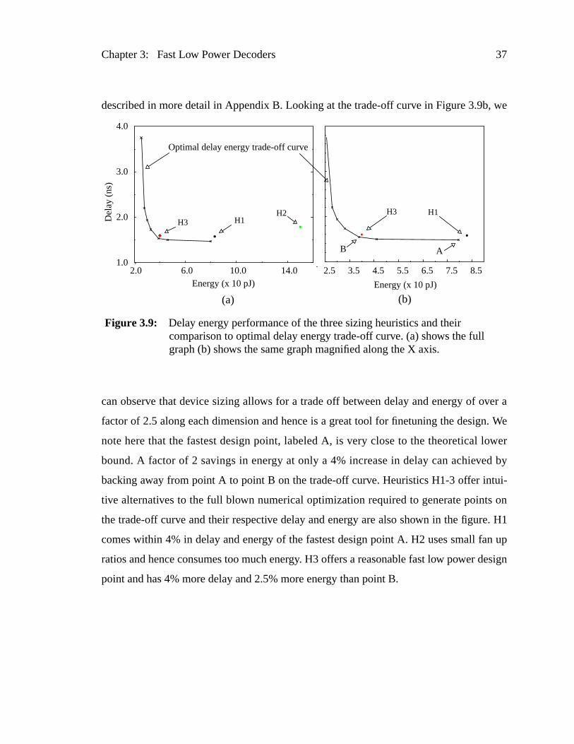
Chapter 3: Fast Low Power Decoders 37
we
ver a
n. We
lower
d by
ui-
s on
e. H1
n up
design
described in more detail in Appendix B. Looking at the trade-off curve in Figure 3.9b,
can observe that device sizing allows for a trade off between delay and energy of o
factor of 2.5 along each dimension and hence is a great tool for finetuning the desig
note here that the fastest design point, labeled A, is very close to the theoretical
bound. A factor of 2 savings in energy at only a 4% increase in delay can achieve
backing away from point A to point B on the trade-off curve. Heuristics H1-3 offer int
tive alternatives to the full blown numerical optimization required to generate point
the trade-off curve and their respective delay and energy are also shown in the figur
comes within 4% in delay and energy of the fastest design point A. H2 uses small fa
ratios and hence consumes too much energy. H3 offers a reasonable fast low power
point and has 4% more delay and 2.5% more energy than point B.
2.0 6.0 10.0 14.0Energy (x 10 pJ)
1.0
2.0
3.0
4.0
Del
ay (
ns)
Optimal delay energy trade-off curve
2.5 3.5 4.5 5.5 6.5 7.5 8.5
Energy (x 10 pJ)
H1H2
H3H1H3
AB
Figure 3.9: Delay energy performance of the three sizing heuristics and theircomparison to optimal delay energy trade-off curve. (a) shows the fullgraph (b) shows the same graph magnified along the X axis.
(a) (b)
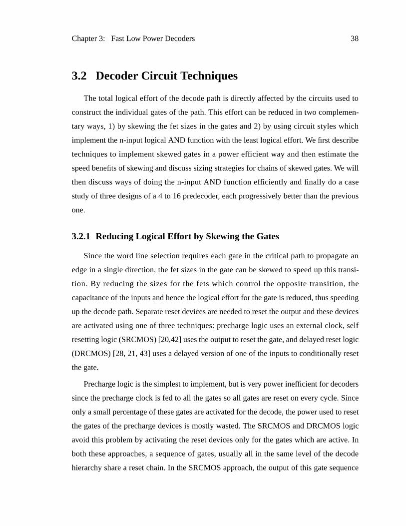
Chapter 3: Fast Low Power Decoders 38
d to
men-
hich
ibe
e the
e will
se
evious
te an
transi-
the
eding
devices
k, self
t logic
eset
ders
. Since
to reset
logic
e. In
ecode
uence
3.2 Decoder Circuit Techniques
The total logical effort of the decode path is directly affected by the circuits use
construct the individual gates of the path. This effort can be reduced in two comple
tary ways, 1) by skewing the fet sizes in the gates and 2) by using circuit styles w
implement the n-input logical AND function with the least logical effort. We first descr
techniques to implement skewed gates in a power efficient way and then estimat
speed benefits of skewing and discuss sizing strategies for chains of skewed gates. W
then discuss ways of doing the n-input AND function efficiently and finally do a ca
study of three designs of a 4 to 16 predecoder, each progressively better than the pr
one.
3.2.1 Reducing Logical Effort by Skewing the Gates
Since the word line selection requires each gate in the critical path to propaga
edge in a single direction, the fet sizes in the gate can be skewed to speed up this
tion. By reducing the sizes for the fets which control the opposite transition,
capacitance of the inputs and hence the logical effort for the gate is reduced, thus spe
up the decode path. Separate reset devices are needed to reset the output and these
are activated using one of three techniques: precharge logic uses an external cloc
resetting logic (SRCMOS) [20,42] uses the output to reset the gate, and delayed rese
(DRCMOS) [28, 21, 43] uses a delayed version of one of the inputs to conditionally r
the gate.
Precharge logic is the simplest to implement, but is very power inefficient for deco
since the precharge clock is fed to all the gates so all gates are reset on every cycle
only a small percentage of these gates are activated for the decode, the power used
the gates of the precharge devices is mostly wasted. The SRCMOS and DRCMOS
avoid this problem by activating the reset devices only for the gates which are activ
both these approaches, a sequence of gates, usually all in the same level of the d
hierarchy share a reset chain. In the SRCMOS approach, the output of this gate seq
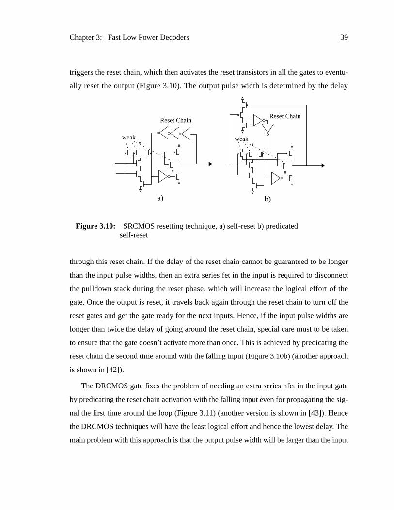
Chapter 3: Fast Low Power Decoders 39
ventu-
elay
longer
nnect
the
ff the
hs are
taken
ing the
roach
gate
sig-
nce
. The
nput
triggers the reset chain, which then activates the reset transistors in all the gates to e
ally reset the output (Figure 3.10). The output pulse width is determined by the d
through this reset chain. If the delay of the reset chain cannot be guaranteed to be
than the input pulse widths, then an extra series fet in the input is required to disco
the pulldown stack during the reset phase, which will increase the logical effort of
gate. Once the output is reset, it travels back again through the reset chain to turn o
reset gates and get the gate ready for the next inputs. Hence, if the input pulse widt
longer than twice the delay of going around the reset chain, special care must to be
to ensure that the gate doesn’t activate more than once. This is achieved by predicat
reset chain the second time around with the falling input (Figure 3.10b) (another app
is shown in [42]).
The DRCMOS gate fixes the problem of needing an extra series nfet in the input
by predicating the reset chain activation with the falling input even for propagating the
nal the first time around the loop (Figure 3.11) (another version is shown in [43]). He
the DRCMOS techniques will have the least logical effort and hence the lowest delay
main problem with this approach is that the output pulse width will be larger than the i
weak
Reset Chain
weak
Reset Chain
a) b)
Figure 3.10: SRCMOS resetting technique, a) self-reset b) predicatedself-reset
Chapter 3: Fast Low Power Decoders 40
s tech-
oken
. Two
issi-
to the
er.
MOS
quire
if-
RAM.
of the
n 4%,
e it is
lock
en-
is a
select
. Also
mber
pulse width and hence not many successive levels of the decode path can use thi
nique before the pulse widths exceed the cycle time.
Thus, the strategy to build the fastest decoder will be to use DRCMOS gates br
occasionally by SRCMOS gates to prevent the pulse widths from becoming too large
external constraints might force a modification of this strategy. One is bitline power d
pation and the other is area overhead. Since the bitline power is directly proportional
local word line pulse width, the latter must be controlled to limit the overall SRAM pow
This implies that the final level of the decode tree has to be implemented in the SRC
style so that its output pulse width can be controlled independently. As these styles re
a lot of fets for doing the reset, implementing the local word driver in this style will sign
icantly add to the memory area, because of the large number of these drivers in the
In a recent design described in [28], we found that the skewed gate implementation
local word driver doubles its area and increases the total memory area by less tha
while it reduces the decode delay by only about 2/3 of a fanout 4 inverter delay. Henc
preferable to implement the preceding decoder level (in the global word driver or the b
select driver) in the SRCMOS style and implement the local word driver in the conv
tional unskewed style. Of the global word driver and the block select driver, the latter
better candidate for the SRCMOS implementation since the reset chain for the block
driver can also be used to clock the sense amplifiers within the block (see Chapter 4)
most SRAM implementations have asymmetric decoder hierarchies in which the nu
weakweak
Predicated Reset
Figure 3.11: A DRCMOS Technique to do local self-resetting of a skewed gate
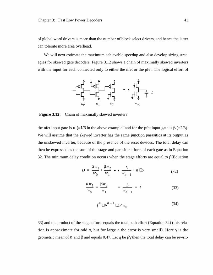
Chapter 3: Fast Low Power Decoders 41
latter
strat-
erters
rt of
put as
lay can
quation
rela-
-
of global word drivers is more than the number of block select drivers, and hence the
can tolerate more area overhead.
We will next estimate the maximum achievable speedup and also develop sizing
egies for skewed gate decoders. Figure 3.12 shows a chain of maximally skewed inv
with the input for each connected only to either the nfet or the pfet. The logical effo
the nfet input gate isα (=1/3 in the above example) and for the pfet input gate isβ (=2/3).
We will assume that the skewed inverter has the same junction parasitics at its out
the unskewed inverter, because of the presence of the reset devices. The total de
then be expressed as the sum of the stage and parasitic efforts of each gate as in E
32. The minimum delay condition occurs when the stage efforts are equal tof (Equation
33) and the product of the stage efforts equals the total path effort (Equation 34) (this
tion is approximate for oddn, but for largen the error is very small). Hereγ is the
geometric mean ofα andβ and equals 0.47. Letq bef/γ then the total delay can be rewrit
L
w0 w1 w2 wn-1
Figure 3.12: Chain of maximally skewed inverters
Dαw1
w0----------
βw2
w1----------+= L
wn 1–-------------- n p⋅+
αw1
w0----------
βw2
w1----------= L
wn 1–--------------= f=
fn γn 1–
L w0⁄⋅∼
(32)
(33)
(34)

Chapter 3: Fast Low Power Decoders 42
at
ence
ut the
total
nd 31
d and
s,
imes
by a
uild-
eries
n an
t, its
fet to
ten as in Equation 35 and optimumq is the solution of Equation 36. We note here th
Equations 34-36 are still valid when the arbitrary skewing strategy providedγ is the geo-
metric mean of all the logical efforts. For p=1.33, Equation 36 results in q~4.8, and h
f ~ 2.4 and the delay per stage is about 30% lower than that for an unskewed chain. B
optimal number of stages is also smaller, giving a net reduction of about 40% for the
delay. For skewed chains with intermediate interconnect, Equations 19, 20, 29, 30 a
are still valid providedf is replaced withq andC, C1, C2 and Lare replaced withC/γ, C1/γ,
C2/γ andL/γ respectively and hence the sizing heuristic H3 can be used for high spee
low power skewed gate decoders too.
3.2.2 Performing an n-input AND Function with Minimum LogicalEffort
The n-input AND function can be implemented via different combination of NAND
NORs and Inverters. Since in current CMOS technologies, a pfet is at least two t
slower than an nfet, NORs are inefficient and so the AND function is best achieved
combination of NANDs and inverters.We will next discuss the three basic styles for b
ing a NAND gate.
3.2.2.1 Conventional Series Stack NAND gate
Figure 3.13a shows the simplest implementation of a 2 input NAND gate in the s
stack topology. In long channel devices, the nfets will be made twice as big as i
inverter, but in sub micron devices, because of velocity saturation in the inverter fe
drive current will not twice as big as in the series stack. For our 0.25µm technology
(Appendix C), the nfets need to be sized to be 1.4 times as large as the inverter n
D γ⁄ n q p γ⁄+( )⋅=
q( )ln 1– p γ⁄q
----------– 0=
(35)
(36)
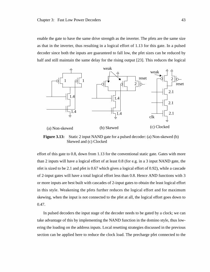
Chapter 3: Fast Low Power Decoders 43
me size
lsed
ced by
ical
ore
cade
h 3
effort
um
n to
e can
ow-
evious
to the
enable the gate to have the same drive strength as the inverter. The pfets are the sa
as that in the inverter, thus resulting in a logical effort of 1.13 for this gate. In a pu
decoder since both the inputs are guaranteed to fall low, the pfet sizes can be redu
half and still maintain the same delay for the rising output [23]. This reduces the log
effort of this gate to 0.8, down from 1.13 for the conventional static gate. Gates with m
than 2 inputs will have a logical effort of at least 0.8 (for e.g. in a 3 input NAND gate, the
nfet is sized to be 2.1 and pfet is 0.67 which gives a logical effort of 0.92), while a cas
of 2-input gates will have a total logical effort less than 0.8. Hence AND functions wit
or more inputs are best built with cascades of 2-input gates to obtain the least logical
in this style. Weakening the pfets further reduces the logical effort and for maxim
skewing, when the input is not connected to the pfet at all, the logical effort goes dow
0.47.
In pulsed decoders the input stage of the decoder needs to be gated by a clock; w
take advantage of this by implementing the NAND function in the domino style, thus l
ering the loading on the address inputs. Local resetting strategies discussed in the pr
section can be applied here to reduce the clock load. The precharge pfet connected
1.4
1.4
1 1
2.1
2.1
2
2.1
(a) Non-skewed
clk1.4
1.4
weak
reset
(b) Skewed (c) Clocked
weak
2 reset
Figure 3.13: Static 2 input NAND gate for a pulsed decoder: (a) Non-skewed (b)Skewed and (c) Clocked

Chapter 3: Fast Low Power Decoders 44
er can
the
driv-
ewed
also
AND
which
ts to
hows
as an
tal
for the
path
right
te in
clock can be weakened and a separate pfet for the precharge which will be much larg
be activated locally within the active gate.
This circuit style is very simple and robust to design in and is well suited for use in
predecoders. In power conscious designs, the input stage of the local and global word
ers will have minimum sized fets to reduce power and hence the gate cannot be sk
much. Since the 2-input NAND gate in this style does no worse than an inverter, it can
be used as the input stage of the word drivers without any delay penalty. But the N
gates at this location can be constructed with fewer fets in the source coupled style
we will discuss next.
3.2.2.2 Source Coupled NAND gate
Two fets can be eliminated from the previous design by applying one of the inpu
the source of an nfet and is called the source coupled style by [24, 26]. Figure 3.14 s
a 2-input NAND implemented using only two fets. This gate can be at least as fast
inverter if the branching effort of the source input is sufficiently large and if the to
capacitance on the source line is much greater than the output load capacitance
gate. To see this, lets compare the delay of the two paths shown in Figure 3.15. The
on the left (labeled A) has the NAND gate embedded within it and the path on the
(labeled B) has an identically sized inverter instead. Both the inputs to the NAND ga
A as well as the input to the inverter in B are driven by inverters of sizew0 through an
2
1
Figure 3.14: Source Coupled NAND gate
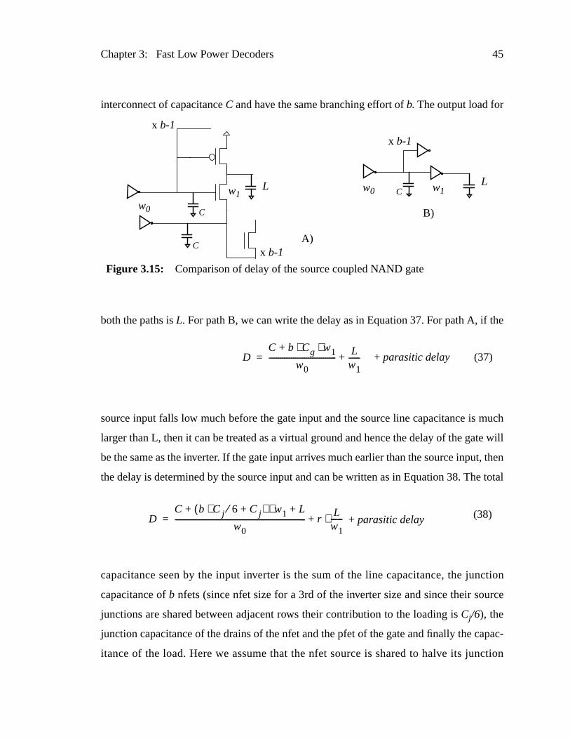
Chapter 3: Fast Low Power Decoders 45
the
much
te will
t, then
total
ction
rce
apac-
ction
interconnect of capacitanceC and have the same branching effort ofb. The output load for
both the paths isL. For path B, we can write the delay as in Equation 37. For path A, if
source input falls low much before the gate input and the source line capacitance is
larger than L, then it can be treated as a virtual ground and hence the delay of the ga
be the same as the inverter. If the gate input arrives much earlier than the source inpu
the delay is determined by the source input and can be written as in Equation 38. The
capacitance seen by the input inverter is the sum of the line capacitance, the jun
capacitance ofb nfets (since nfet size for a 3rd of the inverter size and since their sou
junctions are shared between adjacent rows their contribution to the loading isCj/6), the
junction capacitance of the drains of the nfet and the pfet of the gate and finally the c
itance of the load. Here we assume that the nfet source is shared to halve its jun
L Lw1
x b-1
x b-1
w0
C
x b-1
w1w0
C
C
A)
B)
Figure 3.15: Comparison of delay of the source coupled NAND gate
DC b Cg w1⋅ ⋅+
w0------------------------------------ L
w1------+= (37)+ parasitic delay
DC b Cj 6⁄⋅ Cj+( ) w1⋅ L+ +
w0---------------------------------------------------------------------- r
Lw1------⋅+= (38)+ parasitic delay
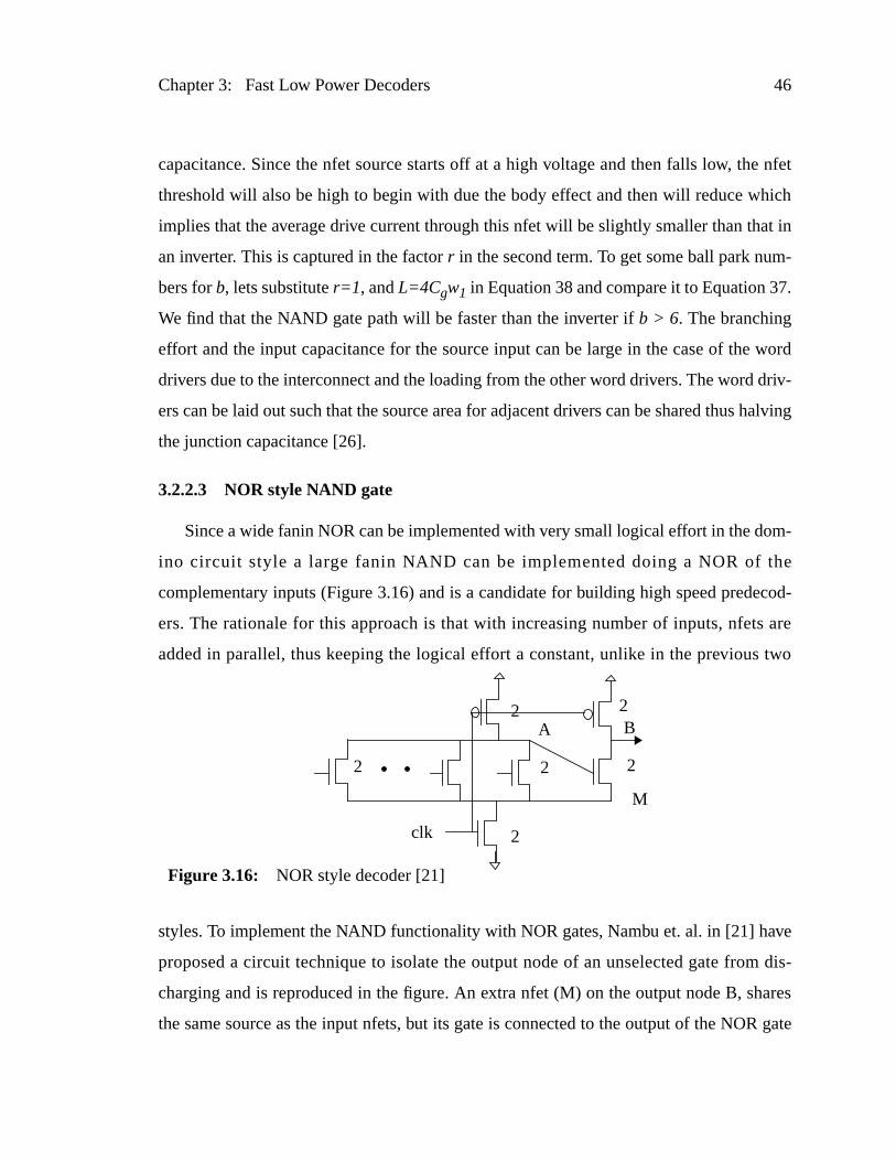
Chapter 3: Fast Low Power Decoders 46
e nfet
ich
at in
-
7.
word
driv-
halving
m-
he
ecod-
s are
two
ve
dis-
ares
R gate
capacitance. Since the nfet source starts off at a high voltage and then falls low, th
threshold will also be high to begin with due the body effect and then will reduce wh
implies that the average drive current through this nfet will be slightly smaller than th
an inverter. This is captured in the factorr in the second term. To get some ball park num
bers forb, lets substituter=1 , andL=4Cgw1 in Equation 38 and compare it to Equation 3
We find that the NAND gate path will be faster than the inverter ifb > 6. The branching
effort and the input capacitance for the source input can be large in the case of the
drivers due to the interconnect and the loading from the other word drivers. The word
ers can be laid out such that the source area for adjacent drivers can be shared thus
the junction capacitance [26].
3.2.2.3 NOR style NAND gate
Since a wide fanin NOR can be implemented with very small logical effort in the do
ino circuit style a large fanin NAND can be implemented doing a NOR of t
complementary inputs (Figure 3.16) and is a candidate for building high speed pred
ers. The rationale for this approach is that with increasing number of inputs, nfet
added in parallel, thus keeping the logical effort a constant, unlike in the previous
styles. To implement the NAND functionality with NOR gates, Nambu et. al. in [21] ha
proposed a circuit technique to isolate the output node of an unselected gate from
charging and is reproduced in the figure. An extra nfet (M) on the output node B, sh
the same source as the input nfets, but its gate is connected to the output of the NO
2
2
22
clk
A B
2
M
2
Figure 3.16: NOR style decoder [21]

Chapter 3: Fast Low Power Decoders 47
oes
then
any of
from
olves
obust
text
is
typi-
stack
kewed
ge in
(A). When clock (clk) is low, both nodes A and B are precharged high. When clock g
high, the behavior of the gate depends on the input values. If all the inputs are low,
node A remains high, while node B discharges and the decoder output is selected. If
the inputs are high, then node A discharges, shutting off M and preventing node B
discharging and hence causing that output to remain unselected. As this situation inv
a race between A and B, the gate needs to be carefully designed to ensure r
operation.
We will next compare this style with the conventional series stack style in the con
of implementing predecoders.
3.2.2.4 Case Study of a 4 to 16 Predecoder
Lets consider the design of a 4 to 16predecoder which needs to drive a load which
equivalent to 76 inverters of size 8 (using the convention of section 3.1). This load is
cal when the predecode line spans 256 rows. We will do a design in both the series
style and the NOR style, and for each consider both the non-skewed as well as the s
versions. To have a fair comparison between the designs, we will size the input sta
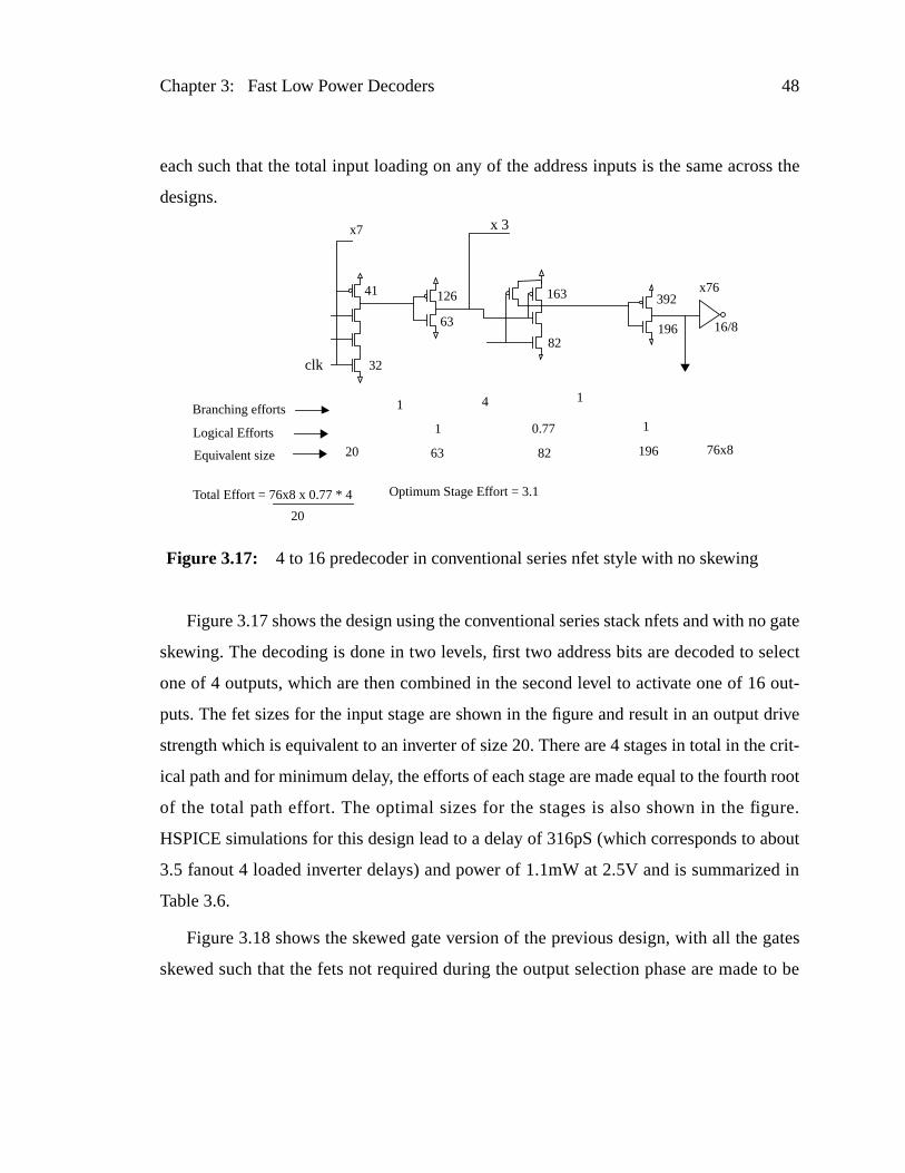
Chapter 3: Fast Low Power Decoders 48
ss the
o gate
elect
out-
drive
crit-
h root
ure.
bout
ed in
gates
to be
each such that the total input loading on any of the address inputs is the same acro
designs.
Figure 3.17 shows the design using the conventional series stack nfets and with n
skewing. The decoding is done in two levels, first two address bits are decoded to s
one of 4 outputs, which are then combined in the second level to activate one of 16
puts. The fet sizes for the input stage are shown in the figure and result in an output
strength which is equivalent to an inverter of size 20. There are 4 stages in total in the
ical path and for minimum delay, the efforts of each stage are made equal to the fourt
of the total path effort. The optimal sizes for the stages is also shown in the fig
HSPICE simulations for this design lead to a delay of 316pS (which corresponds to a
3.5 fanout 4 loaded inverter delays) and power of 1.1mW at 2.5V and is summariz
Table 3.6.
Figure 3.18 shows the skewed gate version of the previous design, with all the
skewed such that the fets not required during the output selection phase are made
x 3
32
41
63
126
82
163
196
392
16/8
x76
x7
Branching efforts 1 4 1
Logical Efforts 1 0.77 1
Equivalent size 20 63 82 196 76x8
Total Effort = 76x8 x 0.77 * 4
20
Optimum Stage Effort = 3.1
clk
Figure 3.17: 4 to 16 predecoder in conventional series nfet style with no skewing
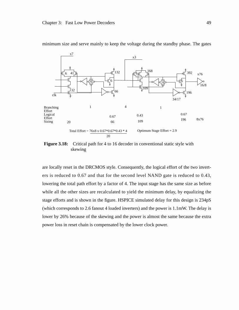
Chapter 3: Fast Low Power Decoders 49
gates
ert-
.43,
efore
the
34pS
lay is
e extra
minimum size and serve mainly to keep the voltage during the standby phase. The
are locally reset in the DRCMOS style. Consequently, the logical effort of the two inv
ers is reduced to 0.67 and that for the second level NAND gate is reduced to 0
lowering the total path effort by a factor of 4. The input stage has the same size as b
while all the other sizes are recalculated to yield the minimum delay, by equalizing
stage efforts and is shown in the figure. HSPICE simulated delay for this design is 2
(which corresponds to 2.6 fanout 4 loaded inverters) and the power is 1.1mW. The de
lower by 26% because of the skewing and the power is almost the same because th
power loss in reset chain is compensated by the lower clock power.
6 41
32
6
132
66
6
x7x3
6
109
168
6
392
196
16/8
x76
34/17
6
clk
BranchingEffortLogicalEffortSizing
1 4 1
0.67 0.43 0.67
20 66 109 196 8x76
Total Effort = 76x8 x 0.67*0.67*0.43 * 4
20
Optimum Stage Effort = 2.9
Figure 3.18: Critical path for 4 to 16 decoder in conventional static style withskewing
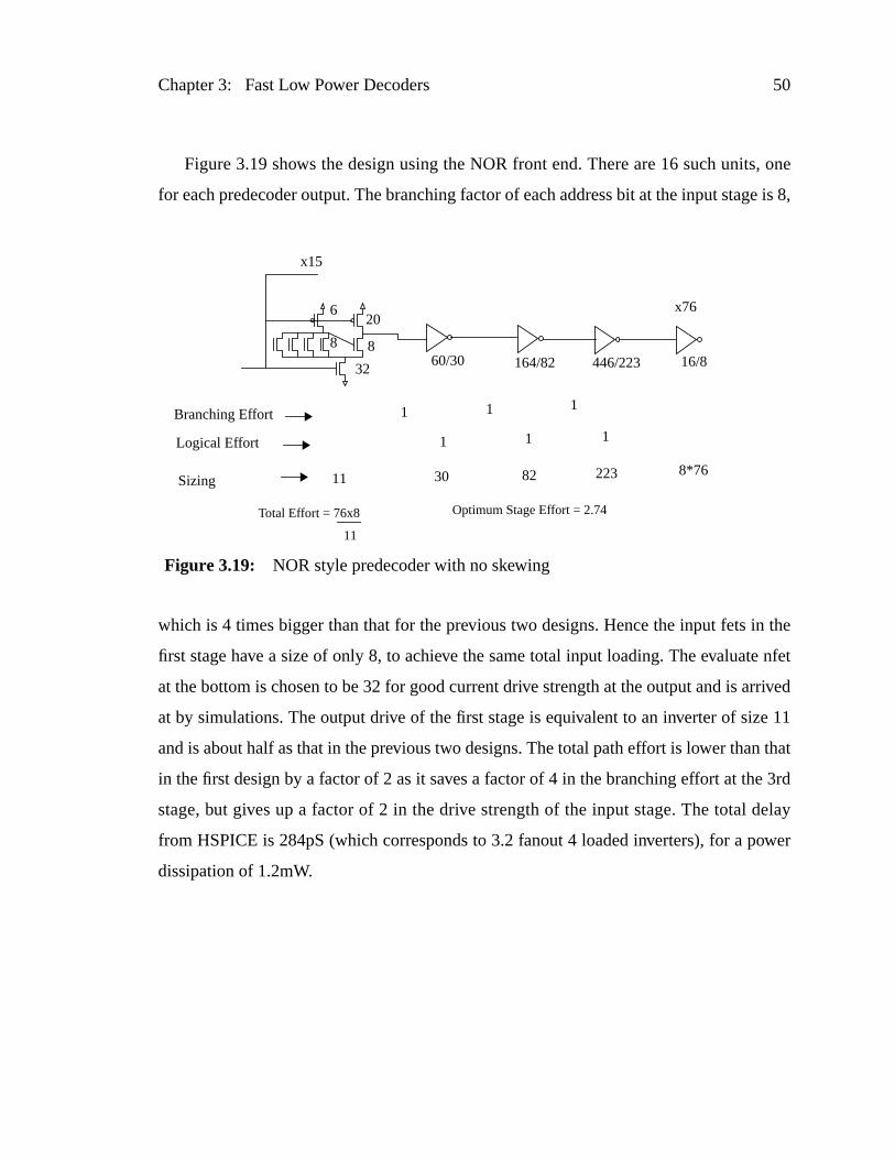
Chapter 3: Fast Low Power Decoders 50
, one
e is 8,
n the
e nfet
rrived
e 11
that
3rd
elay
ower
Figure 3.19 shows the design using the NOR front end. There are 16 such units
for each predecoder output. The branching factor of each address bit at the input stag
which is 4 times bigger than that for the previous two designs. Hence the input fets i
first stage have a size of only 8, to achieve the same total input loading. The evaluat
at the bottom is chosen to be 32 for good current drive strength at the output and is a
at by simulations. The output drive of the first stage is equivalent to an inverter of siz
and is about half as that in the previous two designs. The total path effort is lower than
in the first design by a factor of 2 as it saves a factor of 4 in the branching effort at the
stage, but gives up a factor of 2 in the drive strength of the input stage. The total d
from HSPICE is 284pS (which corresponds to 3.2 fanout 4 loaded inverters), for a p
dissipation of 1.2mW.
32
8
206
860/30 164/82 446/223 16/8
x76
x15
Branching Effort 1 1 1
Logical Effort 1 1 1
Sizing 11 30 82 223 8*76
Total Effort = 76x8
11
Optimum Stage Effort = 2.74
Figure 3.19: NOR style predecoder with no skewing
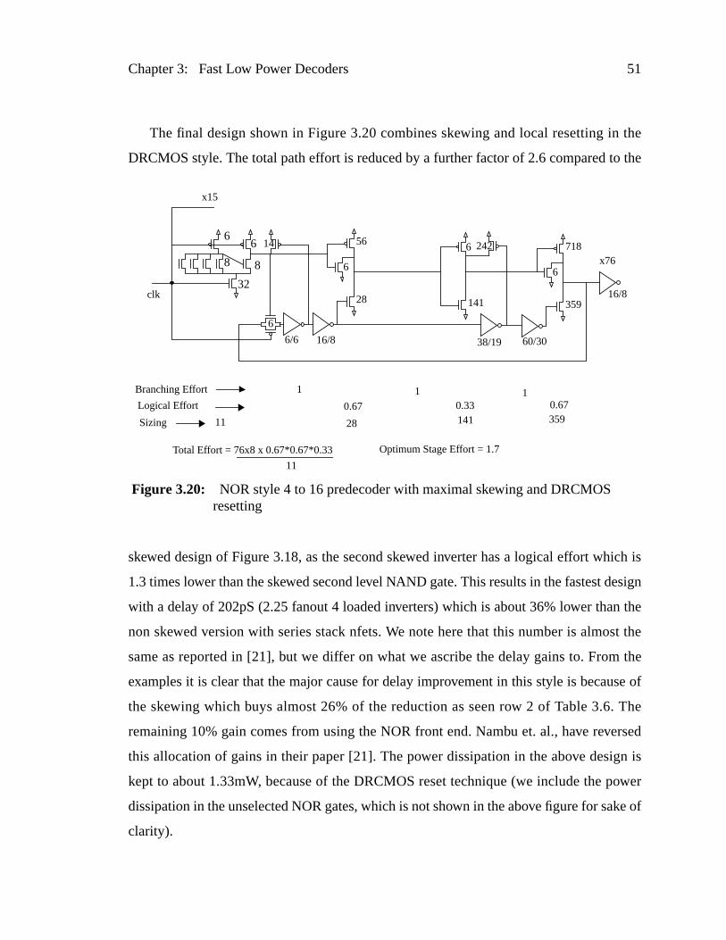
Chapter 3: Fast Low Power Decoders 51
the
the
ich is
esign
the
st the
the
se of
The
rsed
n is
ower
ke of
The final design shown in Figure 3.20 combines skewing and local resetting in
DRCMOS style. The total path effort is reduced by a further factor of 2.6 compared to
skewed design of Figure 3.18, as the second skewed inverter has a logical effort wh
1.3 times lower than the skewed second level NAND gate. This results in the fastest d
with a delay of 202pS (2.25 fanout 4 loaded inverters) which is about 36% lower than
non skewed version with series stack nfets. We note here that this number is almo
same as reported in [21], but we differ on what we ascribe the delay gains to. From
examples it is clear that the major cause for delay improvement in this style is becau
the skewing which buys almost 26% of the reduction as seen row 2 of Table 3.6.
remaining 10% gain comes from using the NOR front end. Nambu et. al., have reve
this allocation of gains in their paper [21]. The power dissipation in the above desig
kept to about 1.33mW, because of the DRCMOS reset technique (we include the p
dissipation in the unselected NOR gates, which is not shown in the above figure for sa
clarity).
32
8
66
8
16/8
x76
14 56
28
6
141
6 718
359
6
6
x15
6/6 16/8
242
38/19 60/30
Branching Effort 1 1 1Logical Effort 0.67 0.33 0.67
Sizing 11 28 141 359
Total Effort = 76x8 x 0.67*0.67*0.33
11
Optimum Stage Effort = 1.7
clk
Figure 3.20: NOR style 4 to 16 predecoder with maximal skewing and DRCMOSresetting
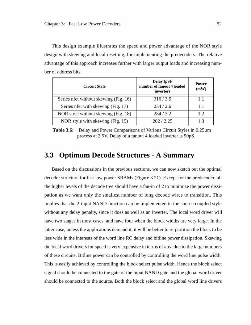
Chapter 3: Fast Low Power Decoders 52
style
lative
num-
ptimal
r, all
dissi-
This
tyle
will
In the
to be
wing
bers
th.
elect
river
rivers
This design example illustrates the speed and power advantage of the NOR
design with skewing and local resetting, for implementing the predecoders. The re
advantage of this approach increases further with larger output loads and increasing
ber of address bits.
3.3 Optimum Decode Structures - A Summary
Based on the discussions in the previous sections, we can now sketch out the o
decoder structure for fast low power SRAMs (Figure 3.21). Except for the predecode
the higher levels of the decode tree should have a fan-in of 2 to minimize the power
pation as we want only the smallest number of long decode wires to transition.
implies that the 2-input NAND function can be implemented in the source coupled s
without any delay penalty, since it does as well as an inverter. The local word driver
have two stages in most cases, and have four when the block widths are very large.
latter case, unless the applications demand it, it will be better to re-partition the block
less wide in the interests of the word line RC delay and bitline power dissipation. Ske
the local word drivers for speed is very expensive in terms of area due to the large num
of these circuits. Bitline power can be controlled by controlling the word line pulse wid
This is easily achieved by controlling the block select pulse width. Hence the block s
signal should be connected to the gate of the input NAND gate and the global word d
should be connected to the source. Both the block select and the global word line d
Circuit StyleDelay (pS)/
number of fanout 4 loadedinverters
Power(mW)
Series nfet without skewing (Fig. 16) 316 / 3.5 1.1
Series nfet with skewing (Fig. 17) 234 / 2.6 1.1
NOR style without skewing (Fig. 18) 284 / 3.2 1.2
NOR style with skewing (Fig. 19) 202 / 2.25 1.3
Table 3.6: Delay and Power Comparisons of Various Circuit Styles in 0.25µmprocess at 2.5V. Delay of a fanout 4 loaded inverter is 90pS.
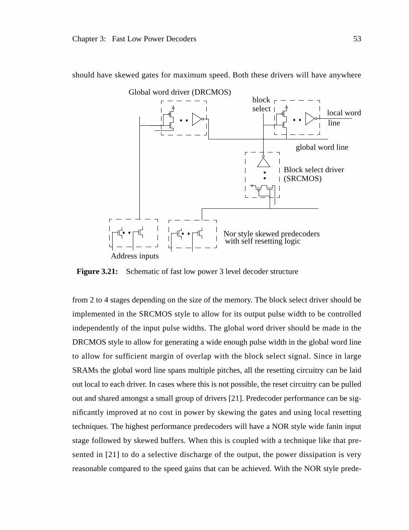
Chapter 3: Fast Low Power Decoders 53
here
ld be
lled
the
line
ge
laid
ulled
be sig-
tting
input
pre-
very
prede-
should have skewed gates for maximum speed. Both these drivers will have anyw
from 2 to 4 stages depending on the size of the memory. The block select driver shou
implemented in the SRCMOS style to allow for its output pulse width to be contro
independently of the input pulse widths. The global word driver should be made in
DRCMOS style to allow for generating a wide enough pulse width in the global word
to allow for sufficient margin of overlap with the block select signal. Since in lar
SRAMs the global word line spans multiple pitches, all the resetting circuitry can be
out local to each driver. In cases where this is not possible, the reset circuitry can be p
out and shared amongst a small group of drivers [21]. Predecoder performance can
nificantly improved at no cost in power by skewing the gates and using local rese
techniques. The highest performance predecoders will have a NOR style wide fanin
stage followed by skewed buffers. When this is coupled with a technique like that
sented in [21] to do a selective discharge of the output, the power dissipation is
reasonable compared to the speed gains that can be achieved. With the NOR style
global word line
local wordline
blockselect
Nor style skewed predecoders
Address inputs
with self resetting logic
Global word driver (DRCMOS)
Block select driver(SRCMOS)
Figure 3.21: Schematic of fast low power 3 level decoder structure
Chapter 3: Fast Low Power Decoders 54
code
AM
. Full
oints.
g as
cant,
ristic,
these
g the
-offs
olves
ther
coder the total path effort becomes independent of the exact partitioning of the de
tree, between the block select and global word decoders. This will allow the SR
designer to choose the best memory organization, based on other considerations.
Transistor sizing offers a great tool to trade off delay and energy of the decoders
blown numerical optimization techniques can be used to obtain the various design p
The simple sizing heuristic of keeping a constant fanout of about 4 works well as lon
the wire delays are not significant. For large memories where the wire delay is signifi
either the wire widths can be increased to reduce their impact or the alternative heu
which relies on calculating the optimal transistor sizes for the gates at the ends of
wires, can be used. For fast lower power solutions, the simple heuristic of reducin
sizes of the input stage in the higher levels of the decode tree allow for good trade
between delay and power.
Getting the decode signal to the local word lines in a fast and low power manner s
half of the memory design problem. We will next look at techniques to solve the o
half, namely build a fast low power data path.
Chapter
iers
mo-
ting
the
ctive
lamp
y of
ines
be
type
s the
nse
or a
lifier
duce
ers,
bitline
4 Fast Low Power SRAMData Path
4.1 Introduction
In an SRAM, switching of the bitlines and I/O lines and biasing the sense amplif
consume a significant fraction of the total power, especially in wide access width me
ries. This chapter investigates techniques to reduce SRAM power without hur
performance by using tracking circuits to limit bitline and I/O line swing, and aid in
generation of the sense clock to enable clocked sense amplifiers.
Traditionally, the bitline swings during a read access have been limited by using a
loads of either diode connected nMOS or resistive pMOS [26, 44]. These devices c
the bitline swing at the expense of a steady bitline current. A more power efficient wa
limiting the bitline swings is to use high impedance bitline loads and pulse the word l
[31-34]. Bitline power can be minimized by controlling the word line pulse width to
just wide enough to guarantee the minimum bitline swing required for sensing. This
of bitline swing control can be achieved by a precise pulse generator that matche
bitline delay. Low power SRAMs also use clocked sense amplifiers to limit the se
power. These amplifiers can be based on either a current mirror [24-25, 45-46]
cross-coupled latch [20-22, 47-48]. In the former, the sense clock turns on the amp
sometime before the sensing, to set up the amplifier in the high gain region. To re
power, the amount of time the amplifier is ON is minimized. In the latch type amplifi
the sense clock starts the amplification and hence the sense clock needs to track the
55
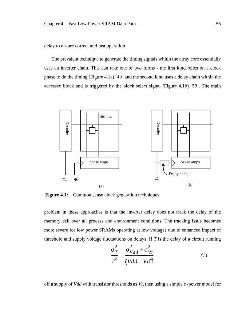
Chapter 4: Fast Low Power SRAM Data Path 56
tially
lock
in the
main
of the
omes
ct of
delay to ensure correct and fast operation.
The prevalent technique to generate the timing signals within the array core essen
uses an inverter chain. This can take one of two forms - the first kind relies on a c
phase to do the timing (Figure 4.1a) [49] and the second kind uses a delay chain with
accessed block and is triggered by the block select signal (Figure 4.1b) [50]. The
problem in these approaches is that the inverter delay does not track the delay
memory cell over all process and environment conditions. The tracking issue bec
more severe for low power SRAMs operating at low voltages due to enhanced impa
threshold and supply voltage fluctuations on delays. IfT is the delay of a circuit running
off a supply ofVddwith transistor thresholds asVt, then using a simpleα-power model for
(a) (b)D
ecoder
Sense amps
Bitlines
Decoder
Sense amps
Delay chainφ1 φ2 φ1
Figure 4.1: Common sense clock generation techniques
σT2
T2
-------σVdd
2 σVt2
+
Vdd Vt–( )2------------------------------∝ (1)
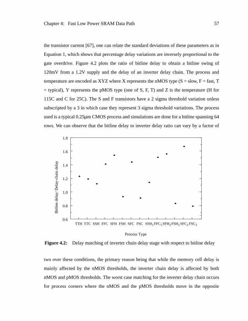
Chapter 4: Fast Low Power SRAM Data Path 57
rs as in
to the
of
and
ast, T
for
s
rocess
64
or of
ay is
both
ccurs
osite
y
the transistor current [67], one can relate the standard deviations of these paramete
Equation 1, which shows that percentage delay variations are inversely proportional
gate overdrive. Figure 4.2 plots the ratio of bitline delay to obtain a bitline swing
120mV from a 1.2V supply and the delay of an inverter delay chain. The process
temperature are encoded as XYZ where X represents the nMOS type (S = slow, F = f
= typical), Y represents the pMOS type (one of S, F, T) and Z is the temperature (H
115C and C for 25C). The S and F transistors have a 2 sigma threshold variation unles
subscripted by a 3 in which case they represent 3 sigma threshold variations. The p
used is a typical 0.25µm CMOS process and simulations are done for a bitline spanning
rows. We can observe that the bitline delay to inverter delay ratio can vary by a fact
two over these conditions, the primary reason being that while the memory cell del
mainly affected by the nMOS thresholds, the inverter chain delay is affected by
nMOS and pMOS thresholds. The worst case matching for the inverter delay chain o
for process corners where the nMOS and the pMOS thresholds move in the opp
TTH TTC SSH FFC SFH FSH SFC FSCSSH3 FFC3 SFH3FSH3 SFC3 FSC3
Process Type
0.6
0.8
1.0
1.2
1.4
1.6
1.8
Bitl
ine
dela
y/ D
elay
-cha
in d
elay
Figure 4.2: Delay matching of inverter chain delay stage with respect to bitline dela
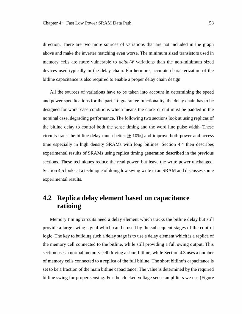
Chapter 4: Fast Low Power SRAM Data Path 58
raph
sed in
d
f the
peed
to be
in the
as of
ese
ss
ibes
ious
anged.
ome
still
ontrol
ica of
his
mber
e is
uired
igure
direction. There are two more sources of variations that are not included in the g
above and make the inverter matching even worse. The minimum sized transistors u
memory cells are more vulnerable todelta-W variations than the non-minimum size
devices used typically in the delay chain. Furthermore, accurate characterization o
bitline capacitance is also required to enable a proper delay chain design.
All the sources of variations have to be taken into account in determining the s
and power specifications for the part. To guarantee functionality, the delay chain has
designed for worst case conditions which means the clock circuit must be padded
nominal case, degrading performance. The following two sections look at using replic
the bitline delay to control both the sense timing and the word line pulse width. Th
circuits track the bitline delay much better [+ 10%] and improve both power and acce
time especially in high density SRAMs with long bitlines. Section 4.4 then descr
experimental results of SRAMs using replica timing generation described in the prev
sections. These techniques reduce the read power, but leave the write power unch
Section 4.5 looks at a technique of doing low swing write in an SRAM and discusses s
experimental results.
4.2 Replica delay element based on capacitanceratioing
Memory timing circuits need a delay element which tracks the bitline delay but
provide a large swing signal which can be used by the subsequent stages of the c
logic. The key to building such a delay stage is to use a delay element which is a repl
the memory cell connected to the bitline, while still providing a full swing output. T
section uses a normal memory cell driving a short bitline, while Section 4.3 uses a nu
of memory cells connected to a replica of the full bitline. The short bitline’s capacitanc
set to be a fraction of the main bitline capacitance. The value is determined by the req
bitline swing for proper sensing. For the clocked voltage sense amplifiers we use (F
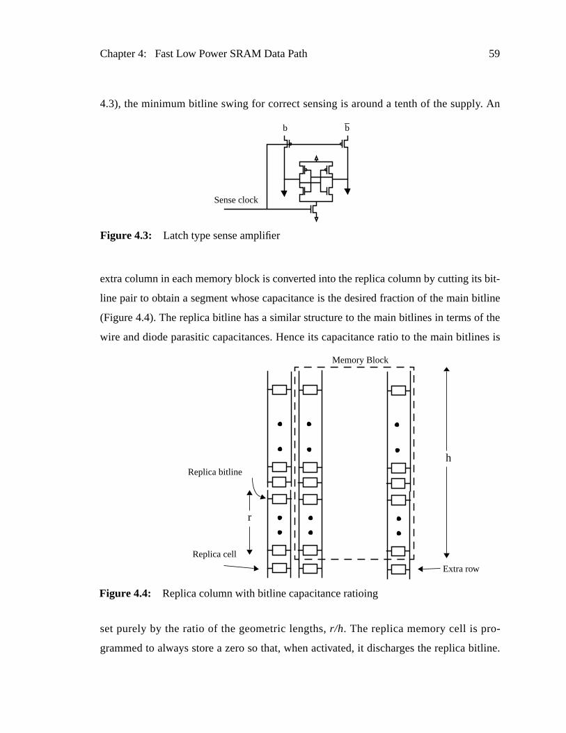
Chapter 4: Fast Low Power SRAM Data Path 59
. An
bit-
itline
f the
nes is
itline.
4.3), the minimum bitline swing for correct sensing is around a tenth of the supply
extra column in each memory block is converted into the replica column by cutting its
line pair to obtain a segment whose capacitance is the desired fraction of the main b
(Figure 4.4). The replica bitline has a similar structure to the main bitlines in terms o
wire and diode parasitic capacitances. Hence its capacitance ratio to the main bitli
set purely by the ratio of the geometric lengths,r/h. The replica memory cell is pro-
grammed to always store a zero so that, when activated, it discharges the replica b
Sense clock
b b
Figure 4.3: Latch type sense amplifier
Extra row
h
r
Memory Block
Replica bitline
Replica cell
Figure 4.4: Replica column with bitline capacitance ratioing
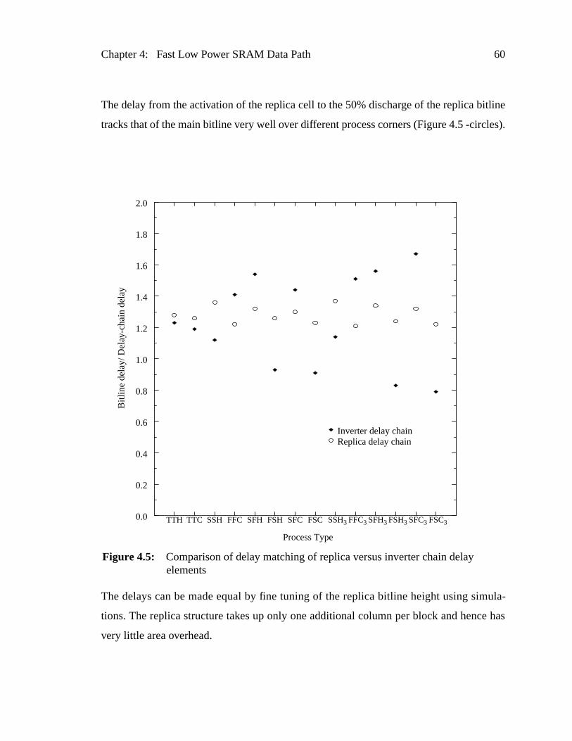
Chapter 4: Fast Low Power SRAM Data Path 60
tline
les).
ula-
e has
The delay from the activation of the replica cell to the 50% discharge of the replica bi
tracks that of the main bitline very well over different process corners (Figure 4.5 -circ
The delays can be made equal by fine tuning of the replica bitline height using sim
tions. The replica structure takes up only one additional column per block and henc
very little area overhead.
TTH TTC SSH FFC SFH FSH SFC FSCSSH3 FFC3 SFH3FSH3 SFC3 FSC3
Process Type
0.0
0.2
0.4
0.6
0.8
1.0
1.2
1.4
1.6
1.8
2.0
Bitl
ine
dela
y/ D
elay
-cha
in d
elay
Inverter delay chainReplica delay chain
Figure 4.5: Comparison of delay matching of replica versus inverter chain delayelements
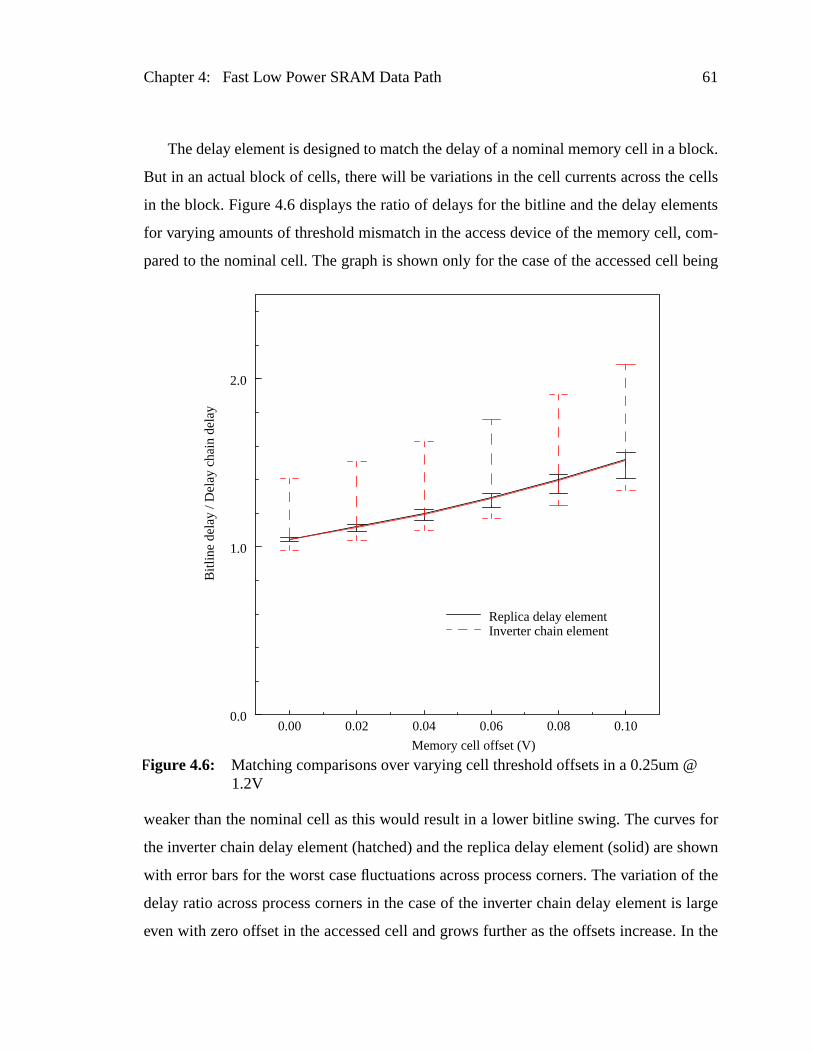
Chapter 4: Fast Low Power SRAM Data Path 61
lock.
cells
ents
com-
being
for
hown
of the
large
In the
The delay element is designed to match the delay of a nominal memory cell in a b
But in an actual block of cells, there will be variations in the cell currents across the
in the block. Figure 4.6 displays the ratio of delays for the bitline and the delay elem
for varying amounts of threshold mismatch in the access device of the memory cell,
pared to the nominal cell. The graph is shown only for the case of the accessed cell
weaker than the nominal cell as this would result in a lower bitline swing. The curves
the inverter chain delay element (hatched) and the replica delay element (solid) are s
with error bars for the worst case fluctuations across process corners. The variation
delay ratio across process corners in the case of the inverter chain delay element is
even with zero offset in the accessed cell and grows further as the offsets increase.
0.00 0.02 0.04 0.06 0.08 0.10
Memory cell offset (V)
0.0
1.0
2.0
Bitl
ine
dela
y / D
elay
cha
in d
elay
Replica delay elementInverter chain element
Figure 4.6: Matching comparisons over varying cell threshold offsets in a 0.25um @1.2V
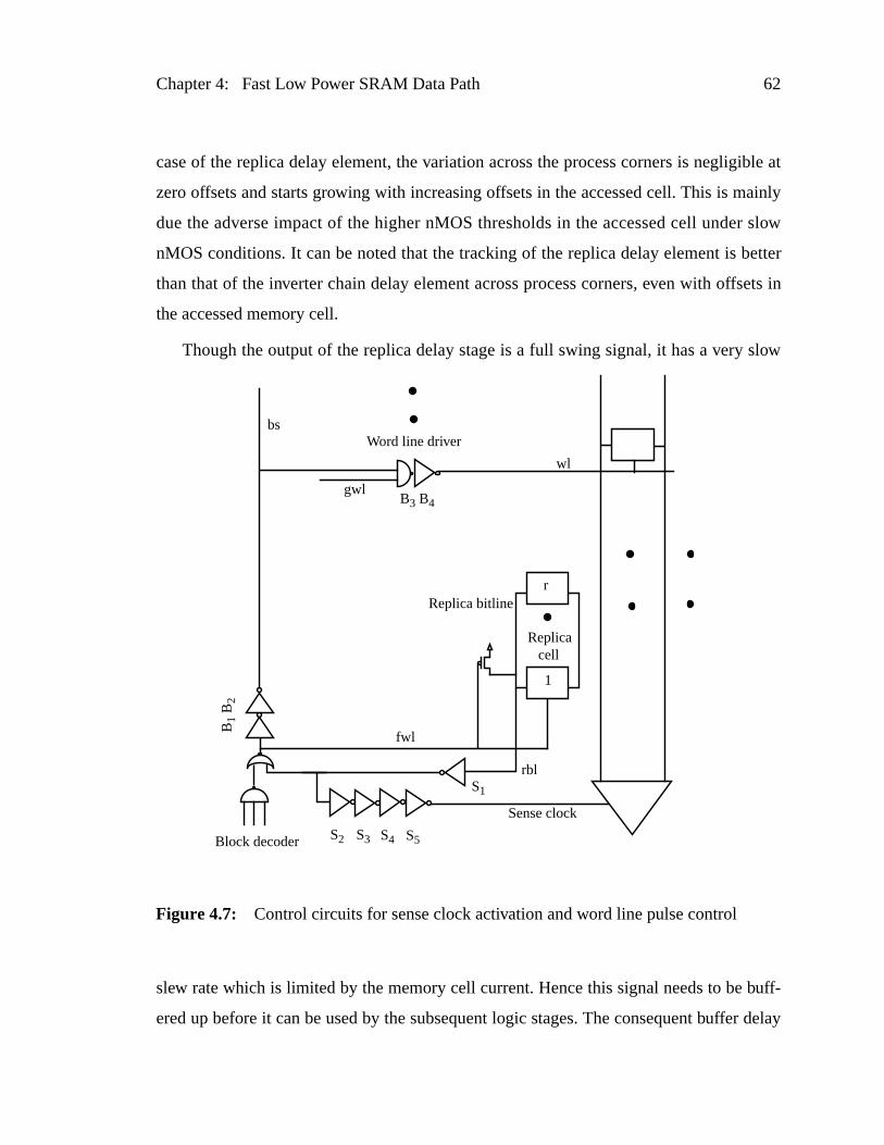
Chapter 4: Fast Low Power SRAM Data Path 62
ible at
ainly
r slow
etter
ets in
low
buff-
r delay
case of the replica delay element, the variation across the process corners is neglig
zero offsets and starts growing with increasing offsets in the accessed cell. This is m
due the adverse impact of the higher nMOS thresholds in the accessed cell unde
nMOS conditions. It can be noted that the tracking of the replica delay element is b
than that of the inverter chain delay element across process corners, even with offs
the accessed memory cell.
Though the output of the replica delay stage is a full swing signal, it has a very s
slew rate which is limited by the memory cell current. Hence this signal needs to be
ered up before it can be used by the subsequent logic stages. The consequent buffe
Replica bitline
Word line driver
wl
Replicacell
fwl
Block decoder
gwl
bs
rbl
1
r
Sense clock
B3 B4
S1
S2 S3 S4
B1
B2
S5
Figure 4.7: Control circuits for sense clock activation and word line pulse control
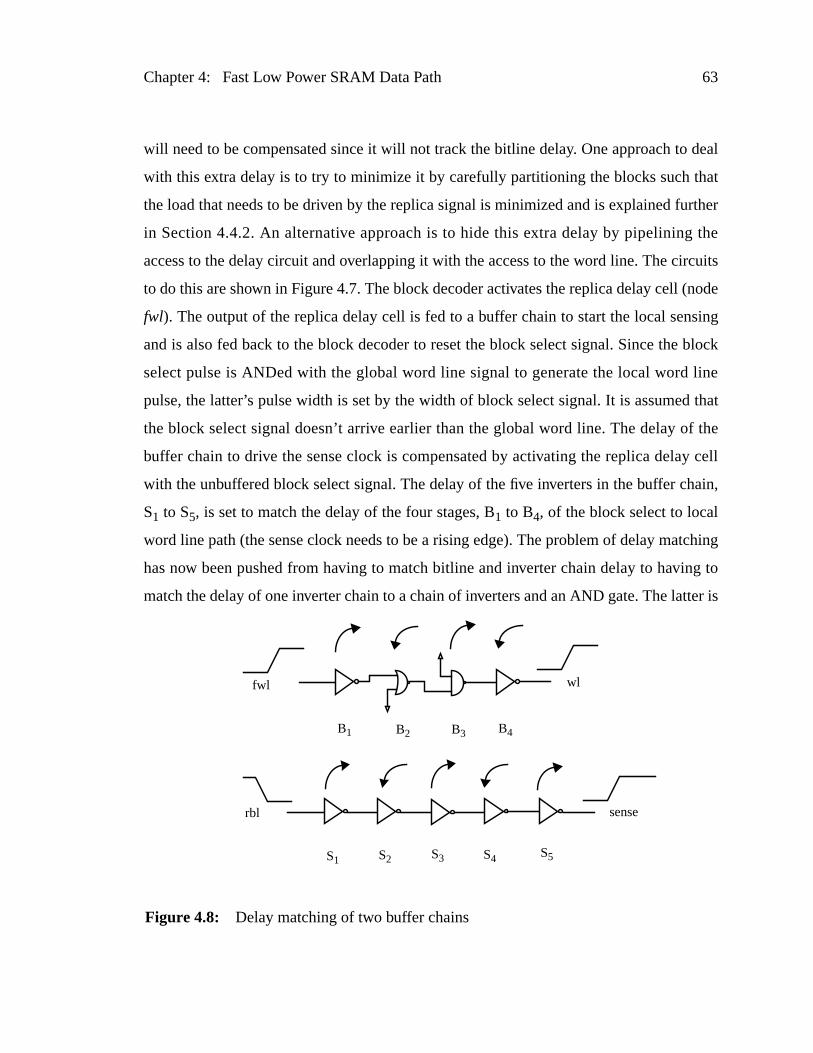
Chapter 4: Fast Low Power SRAM Data Path 63
deal
at
rther
the
cuits
node
sing
block
line
that
f the
y cell
ain,
tching
ng to
ter is
will need to be compensated since it will not track the bitline delay. One approach to
with this extra delay is to try to minimize it by carefully partitioning the blocks such th
the load that needs to be driven by the replica signal is minimized and is explained fu
in Section 4.4.2. An alternative approach is to hide this extra delay by pipelining
access to the delay circuit and overlapping it with the access to the word line. The cir
to do this are shown in Figure 4.7. The block decoder activates the replica delay cell (
fwl). The output of the replica delay cell is fed to a buffer chain to start the local sen
and is also fed back to the block decoder to reset the block select signal. Since the
select pulse is ANDed with the global word line signal to generate the local word
pulse, the latter’s pulse width is set by the width of block select signal. It is assumed
the block select signal doesn’t arrive earlier than the global word line. The delay o
buffer chain to drive the sense clock is compensated by activating the replica dela
with the unbuffered block select signal. The delay of the five inverters in the buffer ch
S1 to S5, is set to match the delay of the four stages, B1 to B4, of the block select to local
word line path (the sense clock needs to be a rising edge). The problem of delay ma
has now been pushed from having to match bitline and inverter chain delay to havi
match the delay of one inverter chain to a chain of inverters and an AND gate. The lat
S1 S2 S3 S4 S5
fwl
rbl sense
wl
B1 B2 B3 B4
Figure 4.8: Delay matching of two buffer chains
Chapter 4: Fast Low Power SRAM Data Path 64
done.
s
he S
and
n the
s over
it-
and
s are
sed
s the
rocess
delay
clock
each
s and
the
of a
amp
r all
tical
r the
excess
easier to tackle, especially since the matching for only one pair of edges needs to be
A simple heuristic for matching the delay of a rising edge of the five long chain, S1 to S5,
to the rising delay of the four long chain, B1 to B4, is to ensure that sum of falling delay
in the two chains are equal as well as the sum of rising delays [51] (Figure 4.8). T
chain has three rising delays and two falling delays while the B chain has two rising
falling delays. This simple sizing technique ensures that the rising and falling delays i
two chains are close to each other giving good delay tracking between the two chain
all process corners. The delay fromfwl (see Figure 4.6) to minimum bitline swing is
tBchain+ tbitline and the delay to the sense clock istreplica + tSchaindelay. If tbitline equals
treplica andtBchainequals tSchain, then the sense clock fires exactly when the minimum b
line swings have developed.
We next look at two design examples, one for a block of 256 rows and 64 columns
the other for a block with 64 rows and 32 columns. The number of rows in these block
typical of large and small SRAMs respectively. For each block the replica ba
implementation is compared to an inverter chain based one. Table 4.1 summarize
simulated performance of the 256 block design over various process corners.Five p
corners are considered along with a 10% supply voltage variation at TT corner. The
elements are designed to yield a bitline swing of around 100mV when the sense
fires, under all conditions with the weakest corner being the SF3 corner with slow nMOS
and fast pMOS (since the memory cell is weak and inverters are relatively faster). For
type of delay element, the table provides the bitline swing when the sense clock fire
the maximum bitline swing after the word line is shut off. An additional column notes
“slack” time of the sense clock with respect to an ideal sense clock, as a fraction
fanout of 4 gate delay. This time indicates the time lost in turning ON of the sense
compared to an ideal sense clock generator which would magically fire unde
conditions exactly when the bitline swings are 100mV, and directly adds to the cri
path delay for the SRAM. The last column shows the excess swing of the bitlines fo
inverter chain case relative to the replica case as a percentage and represents the
Chapter 4: Fast Low Power SRAM Data Path 65
e at
the
at of
ad to
itline
eplica
r the
e gate
ation
ains
f the
pread
d the
bitline power for the former over the latter. The last two rows show the performanc
+10% of the nominal supply of 1.2V in typical conditions. Considering all the rows of
table, we note that the slack time for the replica case is within 2.4 gate delays while th
the inverter case goes up to 5.25 gate delays, indicating that the latter approach will le
a speed specification which is at least 3 gate delays slower than the former. The b
power overhead in the inverter based approach can be up to 40% more than the r
based approach. If we were to consider only correlated threshold fluctuations fo
nMOS and the pMOS, then the delay spread for both the approaches is lower by on
delay, but the relative performance difference still exists. The main reason for the vari
in the slack time for the replica approach is the mismatch in the delays of the buffer ch
across the operating conditions. This comes about mainly due to the variation o
falling edge rate of the replica bitline. In the case of the inverter based design, the s
in slack time comes about due to the lack of tracking between the bitline delay an
Table 4.1: Block parameters: 256 rows, 64 columns
Replica Delay Element (rep-lica bitline height = 29)
Inverter Chain Element
Process,Supply(V)
Bit-lineSwing(mV)
MaxBitlineSwing(mV)
tSlack(as frac-tion offo4del)
Bit-lineSwing(mV)
MaxBitlineSwing(mV)
tSlack(as frac-tion offo4del)a.u.
RelativeMax Bit-line swing(%)
TTH, 1.2 128 136 1.67 139 158 2.24 16.4
FF3, 1.2 114 133 0.64 181 187 4.2 41
SS3, 1.2 136 138 2.37 126 147 1.63 6
SF3, 1.2 97 102 -0.3 101 110 0 7
FS3, 1.2 167 176 2.17 240 251 5.25 43
TTH, 1.08 121 127 1.55 114 134 0.93 5.6
TTH, 1.32 135 145 1.72 172 187 3.64 30
Chapter 4: Fast Low Power SRAM Data Path 66
f the
itline
t and
there
are
ance.
e the
ead
tarts
s the
plica
igure
plifier
inverter chain delay as discussed in the earlier section. To study the scalability o
replica technique, designs for a 64 row block are compared in Table 4.2. The small b
delay for short bitlines, is easy to match even with an inverter chain delay elemen
there is only a slight advantage for the replica design in terms of delay spread while
is not much difference in the maximum bitline swings. The maximum bitline swings
considerably larger than the previous case, mainly due to the smaller bitline capacit
This technique can be modified for clocked current mirror sense amplifiers, wher
exact time of arrival of the sense clock is not critical as long as it arrives sufficiently ah
to setup the amplifiers in the high gain stage by the time the bitline signal s
developing. Delaying the sense clock to be as late as safely possible, minimize
amplifier static power dissipation and can be readily accomplished using the re
techniques. To illustrate this, consider the inverter delay variations in the graph of F
4.5. In order to ensure high performance operation under all process corners, the am
Table 4.2: Block parameters: 64 rows, 32 columns
Replica Delay Element (rep-lica bitline height = 6)
Inverter Chain Element
Process,Supply(V)
Bit-lineSwing(mV)
MaxBitlineSwing(mV)
tSlack(as frac-tion offo4del)
Bit-lineSwing(mV)
MaxBitlineSwing(mV)
tSlack(as frac-tion offo4del)a.u.
RelativeMax Bit-line swing(%)
TTH, 1.2 101 198 0.24 123 192 0.38 -3
FF3, 1.2 100 210 0 162 207 0.85 -1
SS3, 1.2 125 193 0.42 102 177 0 -8
SF3, 1.2 101 155 0 100 145 0 -7.5
FS3, 1.2 110 211 0.1 194 211 1.1 0
TTH, 1.08 113 176 0.24 88 162 -0.24 -8
TTH, 1.32 122 228 0.37 162 223 0.83 -2
Chapter 4: Fast Low Power SRAM Data Path 67
rs,
ing
o the
, the
ings
f the
mber
ll be
what
gnal
zed
times.
ding
to
g the
local
ory
ual to
they
cell
plica
e is
me
delay chain must be fast enough for the FSC3 corner. But then in the other process corne
the amplifier will be turned on much earlier than it needs to and it will be wasting bias
power unnecessarily. If one references the turn on time of the amplifier with respect t
bitline signal development, then for low power operation across process corners
amplifiers need to turn on at some fixed number of gate delays before the bitline sw
develop. This can be achieved via the replica scheme by merely trimming the delay o
S chain with respect to the B chain to ensure that the sense clock turns on a fixed nu
of gate delays before the bitlines differentiate.
While this replica technique generates well controlled sense clock edges, it wi
unable to do the same for the word line pulse widths which turn out to be longer than
is desired for minimum bitline swings. This is mainly because the word line reset si
has to travel back from the replica bitline through the B chain which is usually optimi
to speed up the set signals to assert the local word line in order to reduce the access
In the next section we will describe an alternative replica scheme which allows for fee
the replica signal directly into the word line driver. This will then allow the forward path
assert the local word lines to be optimized using skewed gates [20] without hamperin
local word line pulse width control.
4.3 Replica delay element based on cell current ratioing
An extra row and column containing replica memory cells can be used to provide
resetting timing information for the word line drivers. The extra row contains mem
cells whose pMOS devices are eliminated to act as current sources, with currents eq
that of an accessed memory cell (Figure 4.9). All their outputs are tied together and
simultaneously discharge the replica bitline. This enables a multiple of memory
current to discharge the replica bitline. The current sources are activated by the re
word line which is turned on during each access of the block. The replica bitlin
identical in structure to the main bitlines with dummy memory cells providing the sa
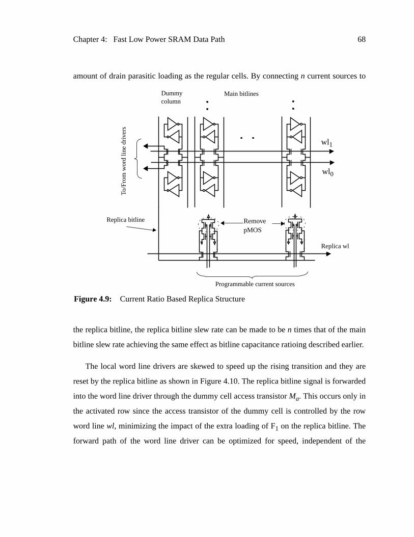
Chapter 4: Fast Low Power SRAM Data Path 68
rlier.
y are
rded
row
the
amount of drain parasitic loading as the regular cells. By connectingn current sources to
the replica bitline, the replica bitline slew rate can be made to ben times that of the main
bitline slew rate achieving the same effect as bitline capacitance ratioing described ea
The local word line drivers are skewed to speed up the rising transition and the
reset by the replica bitline as shown in Figure 4.10. The replica bitline signal is forwa
into the word line driver through the dummy cell access transistorMa. This occurs only in
the activated row since the access transistor of the dummy cell is controlled by the
word linewl, minimizing the impact of the extra loading of F1 on the replica bitline. The
forward path of the word line driver can be optimized for speed, independent of
RemovepMOS
wl0
wl1
Replica wl
Dummycolumn
Main bitlines
Replica bitline
To/F
rom
wor
d lin
e dr
iver
s
Programmable current sources
Figure 4.9: Current Ratio Based Replica Structure

Chapter 4: Fast Low Power SRAM Data Path 69
n in
f the
3 is
resetting of the block select or global word line by skewing the transistors sizes.
The control circuits to activate the replica bitline and the sense clock are show
Figure 4.11. The dummy word line driver is activated by the unbuffered block select,fwl.
The replica bitline is detected by F1 and buffered to drive the sense clock signal. I
delay of the replica bitline is matched with the bitline delay and the delay of F1, S2, S
Table 4.3: Block parameters: 256 rows, 64 columns
Replica Delay Element (rep-lica current sources = 8)
Process,Supply(V)
Bit-line
Swing(mV)
MaxBitlineSwing(mV)
tSlack(as frac-tion offo4del)
TTH, 1.2 120 155 1.2
FF3, 1.2 106 170 0.3
SS3, 1.2 124 155 1.5
SF3, 1.2 94 153 -0.5
FS3, 1.2 144 155 1.53
TTH, 1.08 115 144 1.1
TTH, 1.32 124 172 1.2
Replica Column
DummyCell
F1
rn
weak
bs
gwl wl
Ma
cuthere
Replica Bitline
Figure 4.10: Skewed word line driver
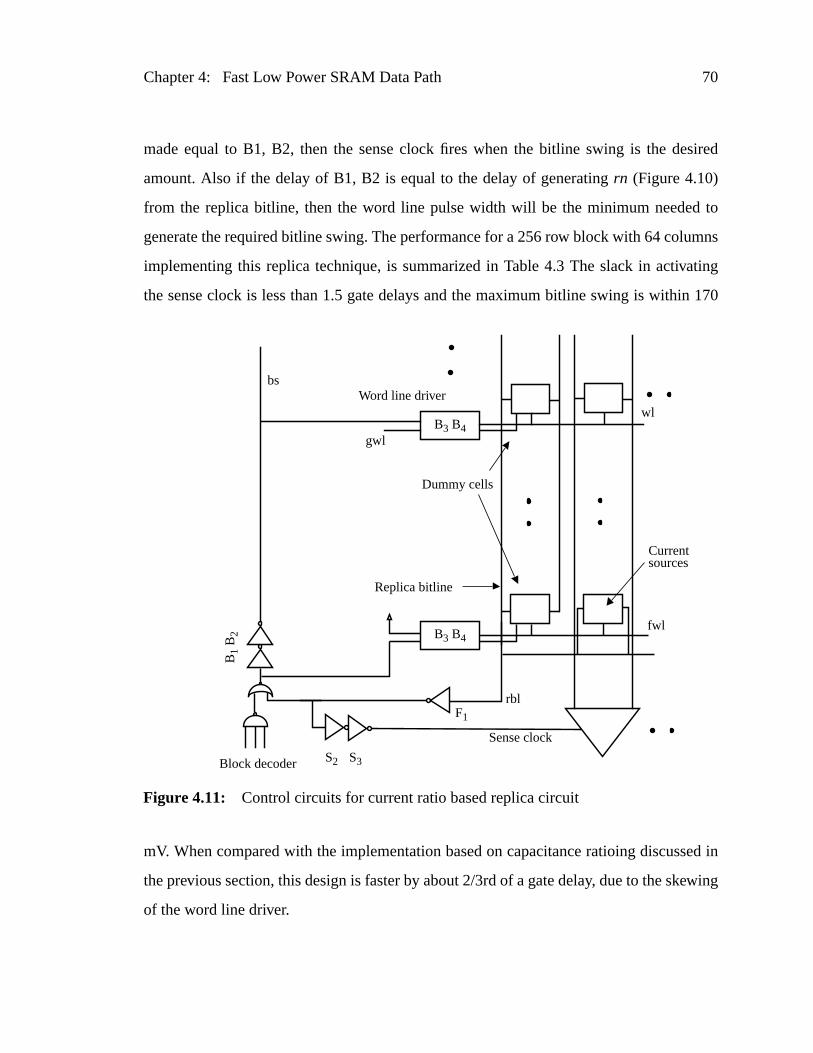
Chapter 4: Fast Low Power SRAM Data Path 70
sired
to
mns
ting
170
sed in
ewing
made equal to B1, B2, then the sense clock fires when the bitline swing is the de
amount. Also if the delay of B1, B2 is equal to the delay of generatingrn (Figure 4.10)
from the replica bitline, then the word line pulse width will be the minimum needed
generate the required bitline swing. The performance for a 256 row block with 64 colu
implementing this replica technique, is summarized in Table 4.3 The slack in activa
the sense clock is less than 1.5 gate delays and the maximum bitline swing is within
mV. When compared with the implementation based on capacitance ratioing discus
the previous section, this design is faster by about 2/3rd of a gate delay, due to the sk
of the word line driver.
Replica bitline
Word line driverwl
fwl
Block decoder
gwl
bs
rbl
Sense clock
B3 B4
F1
S2 S3
B1
B2 B3 B4
Currentsources
Dummy cells
Figure 4.11: Control circuits for current ratio based replica circuit

Chapter 4: Fast Low Power SRAM Data Path 71
plica
comes
n and
ele-
ill be
built
in a
into
the
ber of
two
being
in the
tain
any
t at a
t of
s by
urce.
The power dissipation overhead of this approach is the switching power for the re
bitline which has the same capacitance as the main bitline. The power overhead be
small for large access width SRAMs. The area overhead consists of 1 extra colum
row and the extra area required for the layout of the skewed local word line drivers.
4.4 Measured Results
We designed and tested two prototype chips with both kinds of replica delay
ment.The first chip is a 8Kbit RAM built in a MOSIS 1.2µm process and has the
capacitance ratioing replica besides some other low power techniques and w
described next. Following that we will discuss the second prototype chip which was
in a 0.25µm process from TI and includes the replica based on cell current ratioing.
4.4.1 SRAM test chip with replica feedback based on capacitanceratioing
The replica feedback technique based on capacitive ratioing was implemented
1.2µm process as part of a 2k x 32 SRAM [27-28]. The SRAM array was partitioned
eight blocks each with 256 rows and 32 columns. Making the block width equal to
access width ensures that the bitline power is minimized since only the desired num
bitline columns swing in any access. Two extra columns near the word line drivers and
extra rows near the sense amps are provided for each block with the replica column
the second one from the word line drivers and the replica cell being the second cell
column (Figure 4.12). The extra row and column surrounding the replica cell con
dummy cells for padding purposes, so that the replica cell doesn’t suffer from
processing variations at the array edge. The bitlines in the replica column are cu
height of 26 rows, yielding a capacitance for the replica bitline which is one tenth tha
the main bitline. Further control for the replica delay is provided for testing purpose
utilizing part of the replica structure above the cut to provide an adjustable current so
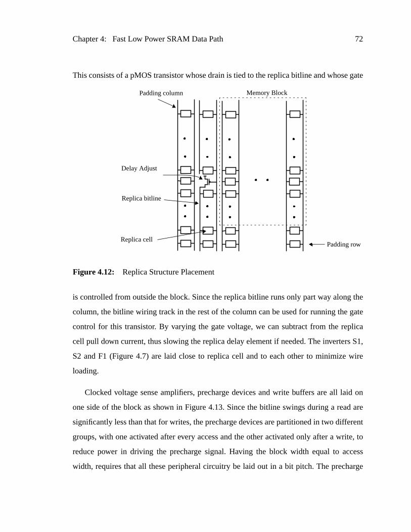
Chapter 4: Fast Low Power SRAM Data Path 72
gate
the
gate
lica
s S1,
wire
id on
d are
rent
ite, to
cess
arge
This consists of a pMOS transistor whose drain is tied to the replica bitline and whose
is controlled from outside the block. Since the replica bitline runs only part way along
column, the bitline wiring track in the rest of the column can be used for running the
control for this transistor. By varying the gate voltage, we can subtract from the rep
cell pull down current, thus slowing the replica delay element if needed. The inverter
S2 and F1 (Figure 4.7) are laid close to replica cell and to each other to minimize
loading.
Clocked voltage sense amplifiers, precharge devices and write buffers are all la
one side of the block as shown in Figure 4.13. Since the bitline swings during a rea
significantly less than that for writes, the precharge devices are partitioned in two diffe
groups, with one activated after every access and the other activated only after a wr
reduce power in driving the precharge signal. Having the block width equal to ac
width, requires that all these peripheral circuitry be laid out in a bit pitch. The prech
Padding row
Memory Block
Replica bitline
Replica cell
Padding column
Delay Adjust
Figure 4.12: Replica Structure Placement
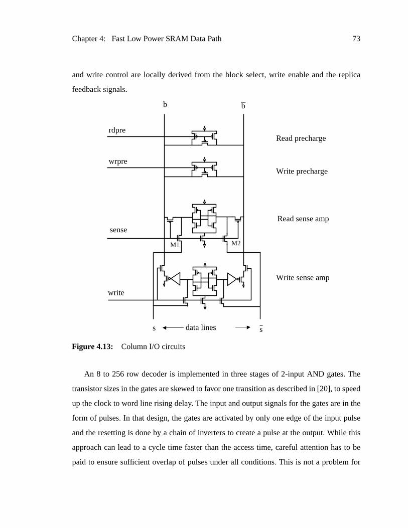
Chapter 4: Fast Low Power SRAM Data Path 73
lica
The
speed
n the
pulse
le this
to be
for
and write control are locally derived from the block select, write enable and the rep
feedback signals.
An 8 to 256 row decoder is implemented in three stages of 2-input AND gates.
transistor sizes in the gates are skewed to favor one transition as described in [20], to
up the clock to word line rising delay. The input and output signals for the gates are i
form of pulses. In that design, the gates are activated by only one edge of the input
and the resetting is done by a chain of inverters to create a pulse at the output. Whi
approach can lead to a cycle time faster than the access time, careful attention has
paid to ensure sufficient overlap of pulses under all conditions. This is not a problem
wrpre
sense
write
b b
s s
rdpre
Write sense amp
Read sense amp
Write precharge
Read precharge
data lines
Figure 4.13: Column I/O circuits
M1 M2
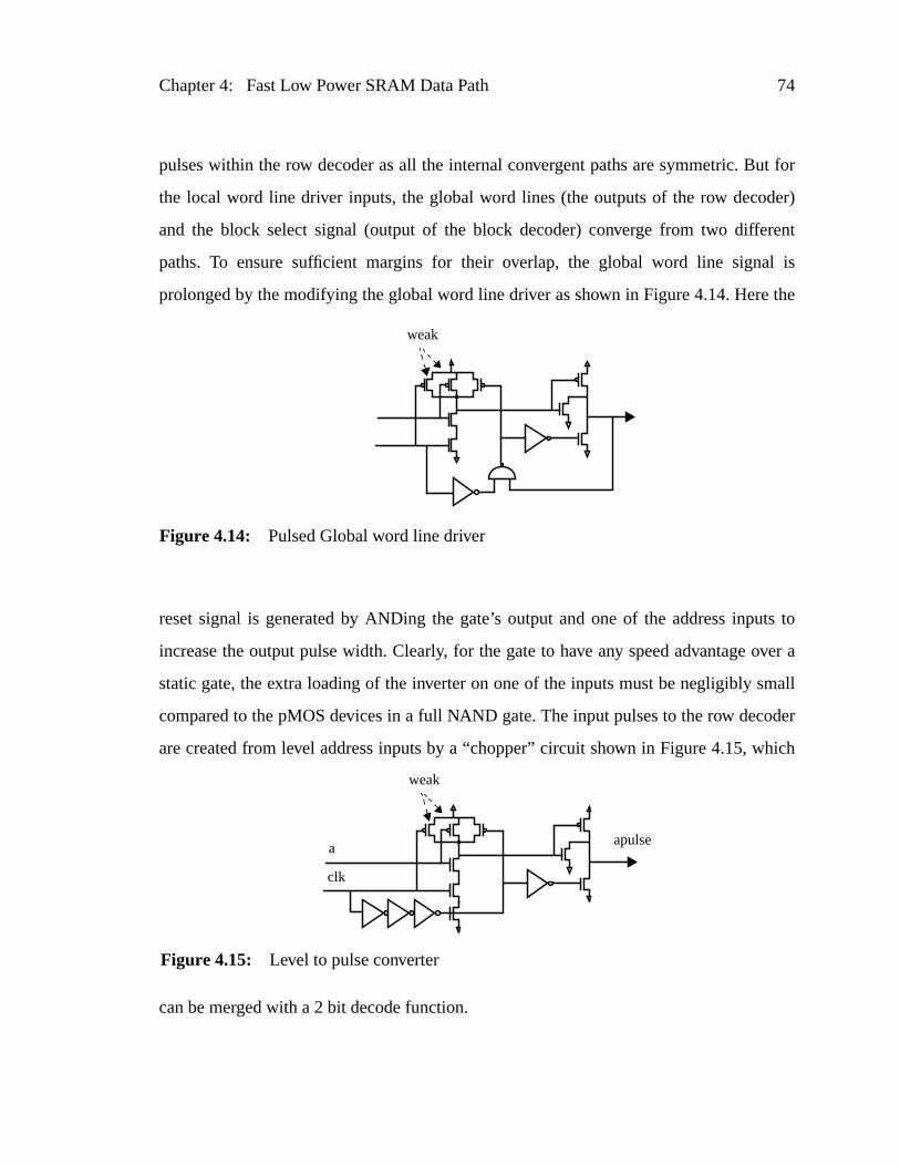
Chapter 4: Fast Low Power SRAM Data Path 74
ut for
der)
rent
l is
the
uts to
over a
mall
oder
hich
pulses within the row decoder as all the internal convergent paths are symmetric. B
the local word line driver inputs, the global word lines (the outputs of the row deco
and the block select signal (output of the block decoder) converge from two diffe
paths. To ensure sufficient margins for their overlap, the global word line signa
prolonged by the modifying the global word line driver as shown in Figure 4.14. Here
reset signal is generated by ANDing the gate’s output and one of the address inp
increase the output pulse width. Clearly, for the gate to have any speed advantage
static gate, the extra loading of the inverter on one of the inputs must be negligibly s
compared to the pMOS devices in a full NAND gate. The input pulses to the row dec
are created from level address inputs by a “chopper” circuit shown in Figure 4.15, w
can be merged with a 2 bit decode function.
weak
Figure 4.14: Pulsed Global word line driver
weak
a
clk
apulse
Figure 4.15: Level to pulse converter
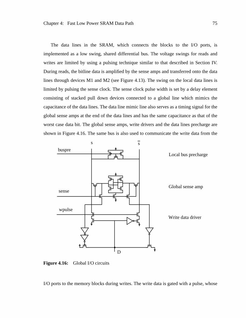
Chapter 4: Fast Low Power SRAM Data Path 75
, is
and
IV.
e data
es is
ment
the
or the
at of the
rge are
m the
hose
The data lines in the SRAM, which connects the blocks to the I/O ports
implemented as a low swing, shared differential bus. The voltage swings for reads
writes are limited by using a pulsing technique similar to that described in Section
During reads, the bitline data is amplified by the sense amps and transferred onto th
lines through devices M1 and M2 (see Figure 4.13). The swing on the local data lin
limited by pulsing the sense clock. The sense clock pulse width is set by a delay ele
consisting of stacked pull down devices connected to a global line which mimics
capacitance of the data lines. The data line mimic line also serves as a timing signal f
global sense amps at the end of the data lines and has the same capacitance as th
worst case data bit. The global sense amps, write drivers and the data lines precha
shown in Figure 4.16. The same bus is also used to communicate the write data fro
I/O ports to the memory blocks during writes. The write data is gated with a pulse, w
buspre
sense
wpulse
Local bus precharge
Global sense amp
Write data driver
D
s s
Figure 4.16: Global I/O circuits
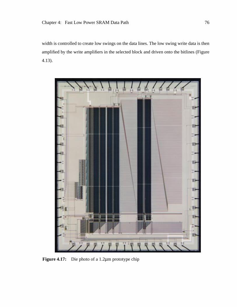
Chapter 4: Fast Low Power SRAM Data Path 76
then
ure
width is controlled to create low swings on the data lines. The low swing write data is
amplified by the write amplifiers in the selected block and driven onto the bitlines (Fig
4.13).
Figure 4.17: Die photo of a 1.2µm prototype chip
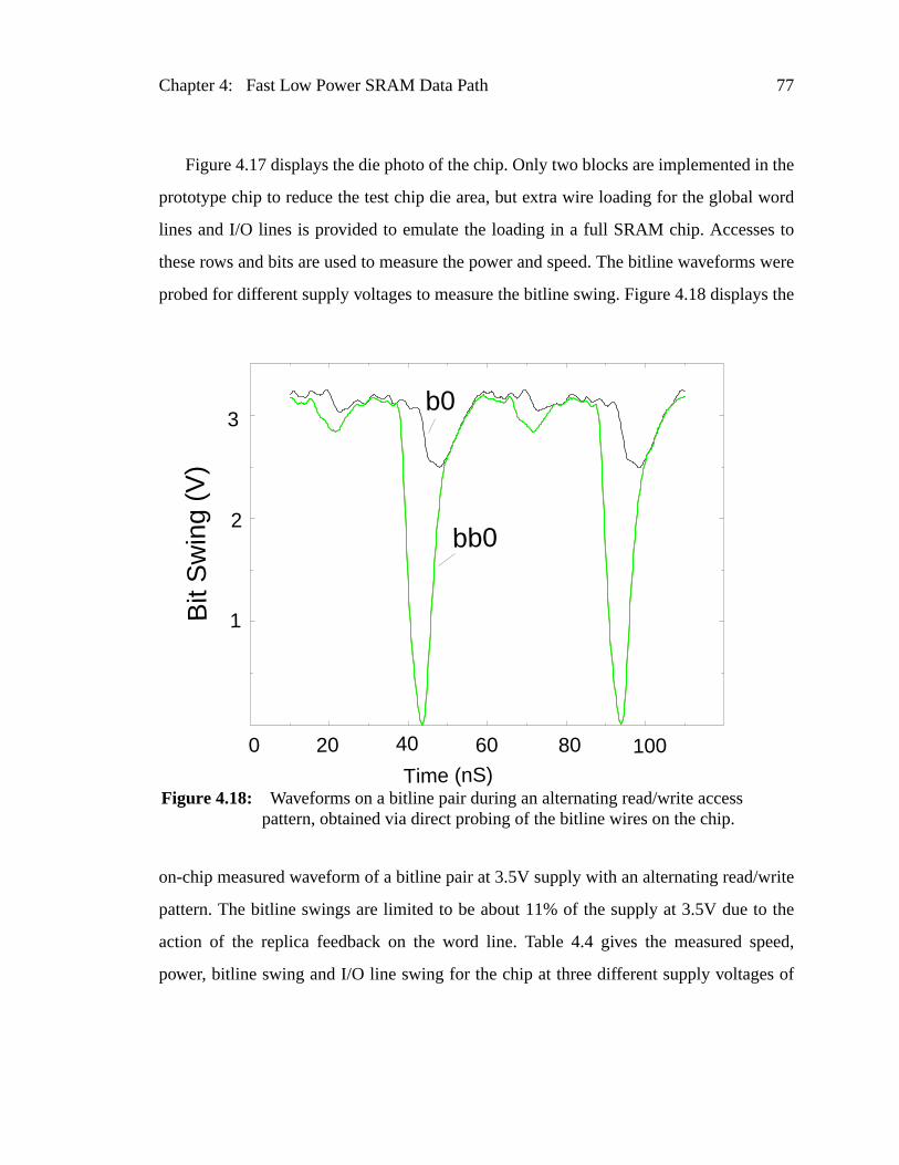
Chapter 4: Fast Low Power SRAM Data Path 77
the
word
s to
s were
s the
rite
the
peed,
of
Figure 4.17 displays the die photo of the chip. Only two blocks are implemented in
prototype chip to reduce the test chip die area, but extra wire loading for the global
lines and I/O lines is provided to emulate the loading in a full SRAM chip. Accesse
these rows and bits are used to measure the power and speed. The bitline waveform
probed for different supply voltages to measure the bitline swing. Figure 4.18 display
on-chip measured waveform of a bitline pair at 3.5V supply with an alternating read/w
pattern. The bitline swings are limited to be about 11% of the supply at 3.5V due to
action of the replica feedback on the word line. Table 4.4 gives the measured s
power, bitline swing and I/O line swing for the chip at three different supply voltages
Time (nS)
Bit
Sw
ing
(V)
bb0
b0
0 20 40 60 80 100
1
2
3
Figure 4.18: Waveforms on a bitline pair during an alternating read/write accesspattern, obtained via direct probing of the bitline wires on the chip.
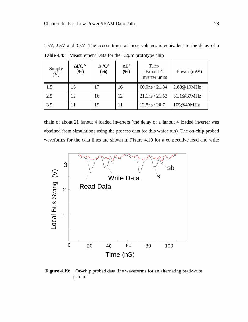
Chapter 4: Fast Low Power SRAM Data Path 78
y of a
was
obed
write
1.5V, 2.5V and 3.5V. The access times at these voltages is equivalent to the dela
chain of about 21 fanout 4 loaded inverters (the delay of a fanout 4 loaded inverter
obtained from simulations using the process data for this wafer run). The on-chip pr
waveforms for the data lines are shown in Figure 4.19 for a consecutive read and
Table 4.4: Measurement Data for the 1.2µm prototype chip
Supply(V)
∆I/Ow
(%)∆I/Or
(%)∆Br
(%)Tacc/
Fanout 4Inverter units
Power (mW)
1.5 16 17 16 60.0ns / 21.84 2.88@10MHz
2.5 12 16 12 21.1ns / 21.53 31.1@37MHz
3.5 11 19 11 12.8ns / 20.7 105@40MHz
0 20 40 60 80 100
1
2
3
Time (nS)
Loca
l Bus
Sw
ing
(V
)
ssb
Read DataWrite Data
Figure 4.19: On-chip probed data line waveforms for an alternating read/writepattern

Chapter 4: Fast Low Power SRAM Data Path 79
are
ng of
s
the
next
Kbit
word
iving
t the
ca of
ical
plica
ding
line
arges
dress
lay
in this
as to
plica
gure
operation. The I/O bus swings for writes are limited to 11% of the supply at 3.5V, but
19% of the supply for reads. The rather large read swings is due to improper matchi
the sense amplifier replica circuit with the read sense amplifiers.
4.4.2 SRAM test chip with replica feedback based on cell currentratioing
Cell current ratioing based replica technique was implemented in a 0.25µm process
(with wire pitch based on a 0.35µm process) from Texas Instruments. A 2KB RAM i
partitioned into two blocks of 256 rows by 32 columns. Two extra rows are added to
top of each block, with the topmost row serving as a padding for the array and the
row containing the replica cells.
The prototype chip (Figure 4.20) has 2 blocks each 256 rows x 32 bits to form a 8
memory. The premise in this chip was that the delay relationship between the global
line and the block select is unknown, i.e, either one of them could be the late arr
signal and hence the local word line could be triggered by either. This implies tha
replica bitline path too needs to be activated by either the local block select or a repli
the global word line. The replica of the global word line is created by mirroring the crit
path of the row decoders as shown in Figure 4.21. This involves creating re
predecoders, global word drivers, replica predecode and global word lines with loa
identical to the main predecode and global word lines [53]. The replica global word
and the block select signal in each block generate the replica word line which disch
the replica bitline as described in the previous section. Thus the delay from the ad
inputs to the bitline is mirrored in the delay to the replica bitlines. But the additional de
of buffering this replica bitline to generate the sense amp signal cannot be cancelled
approach. Hence the only alternative to minimize this overhead in our prototype w
distribute the replica bitline structure throughout the array. The test chip has one re
bitline structure per eight bitline columns, with just one sense clock buffer stage (Fi
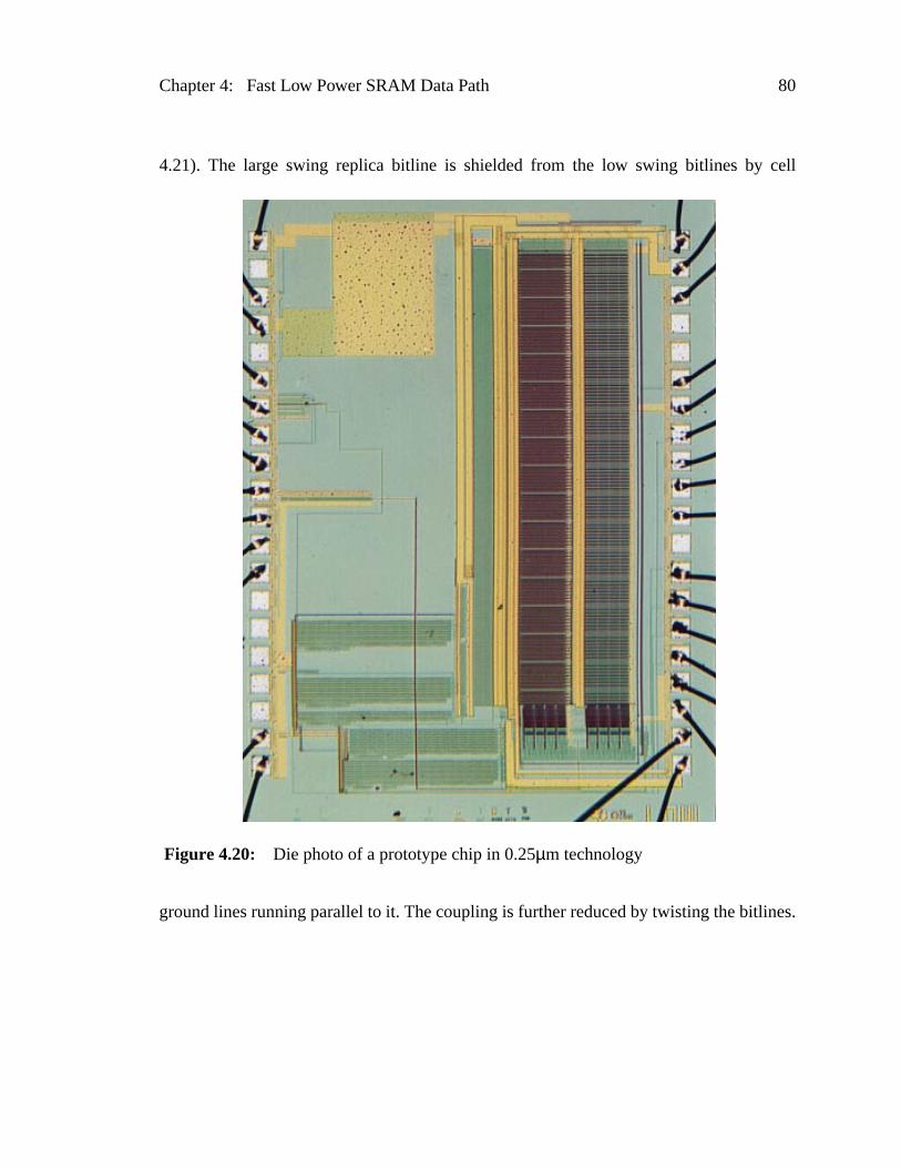
Chapter 4: Fast Low Power SRAM Data Path 80
ell
es.
4.21). The large swing replica bitline is shielded from the low swing bitlines by c
ground lines running parallel to it. The coupling is further reduced by twisting the bitlin
Figure 4.20: Die photo of a prototype chip in 0.25µm technology
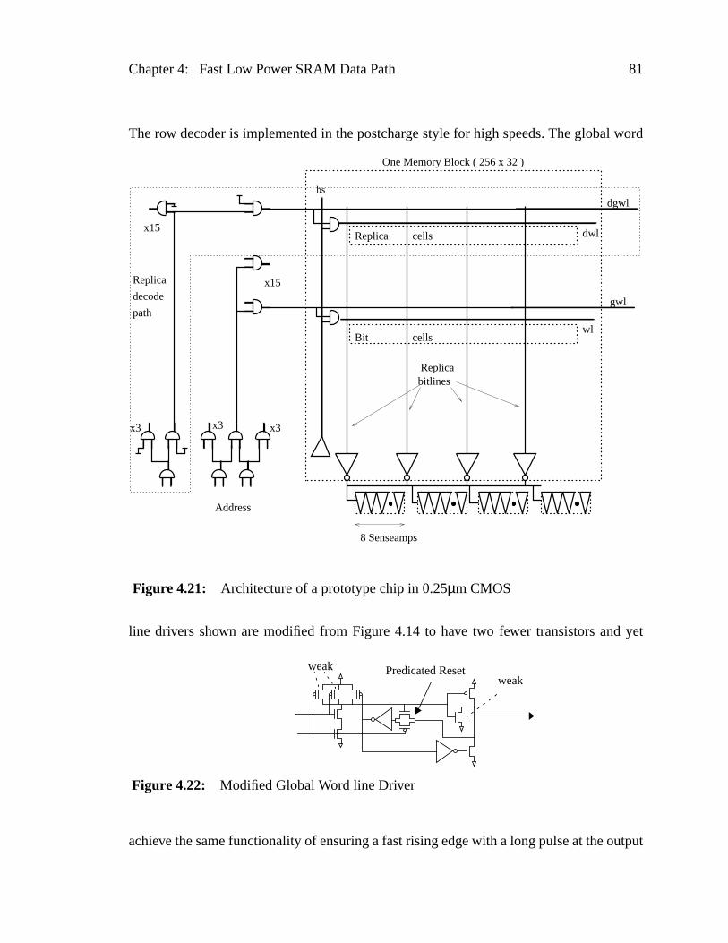
Chapter 4: Fast Low Power SRAM Data Path 81
word
yet
utput
The row decoder is implemented in the postcharge style for high speeds. The global
line drivers shown are modified from Figure 4.14 to have two fewer transistors and
achieve the same functionality of ensuring a fast rising edge with a long pulse at the o
bs
x3
x15
x3x3
x15
One Memory Block ( 256 x 32 )
Address
Replica
decode
path
8 Senseamps
Replicabitlines
dgwl
dwl
gwl
wl
Replica cells
Bit cells
Figure 4.21: Architecture of a prototype chip in 0.25µm CMOS
weakweak
Predicated Reset
Figure 4.22: Modified Global Word line Driver
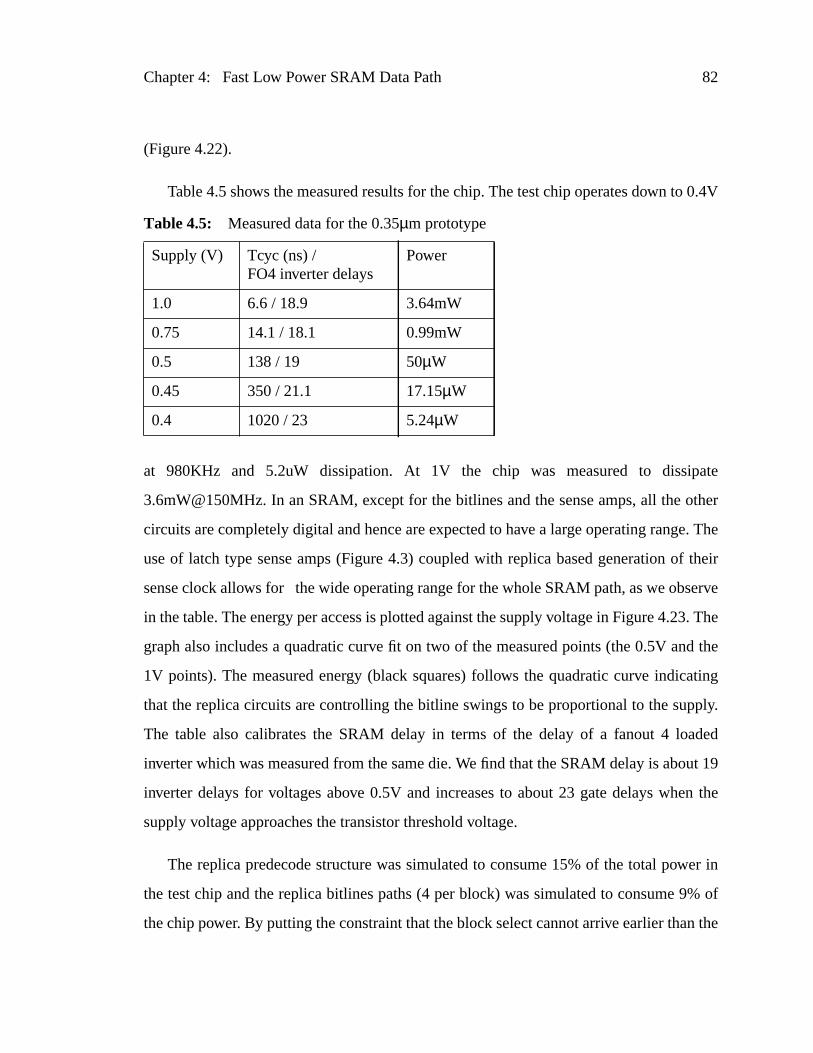
Chapter 4: Fast Low Power SRAM Data Path 82
0.4V
ate
other
e. The
f their
serve
3. The
d the
ating
ply.
ded
ut 19
en the
er in
% of
n the
(Figure 4.22).
Table 4.5 shows the measured results for the chip. The test chip operates down to
at 980KHz and 5.2uW dissipation. At 1V the chip was measured to dissip
3.6mW@150MHz. In an SRAM, except for the bitlines and the sense amps, all the
circuits are completely digital and hence are expected to have a large operating rang
use of latch type sense amps (Figure 4.3) coupled with replica based generation o
sense clock allows for the wide operating range for the whole SRAM path, as we ob
in the table. The energy per access is plotted against the supply voltage in Figure 4.2
graph also includes a quadratic curve fit on two of the measured points (the 0.5V an
1V points). The measured energy (black squares) follows the quadratic curve indic
that the replica circuits are controlling the bitline swings to be proportional to the sup
The table also calibrates the SRAM delay in terms of the delay of a fanout 4 loa
inverter which was measured from the same die. We find that the SRAM delay is abo
inverter delays for voltages above 0.5V and increases to about 23 gate delays wh
supply voltage approaches the transistor threshold voltage.
The replica predecode structure was simulated to consume 15% of the total pow
the test chip and the replica bitlines paths (4 per block) was simulated to consume 9
the chip power. By putting the constraint that the block select cannot arrive earlier tha
Table 4.5: Measured data for the 0.35µm prototype
Supply (V) Tcyc (ns) /FO4 inverter delays
Power
1.0 6.6 / 18.9 3.64mW
0.75 14.1 / 18.1 0.99mW
0.5 138 / 19 50µW
0.45 350 / 21.1 17.15µW
0.4 1020 / 23 5.24µW
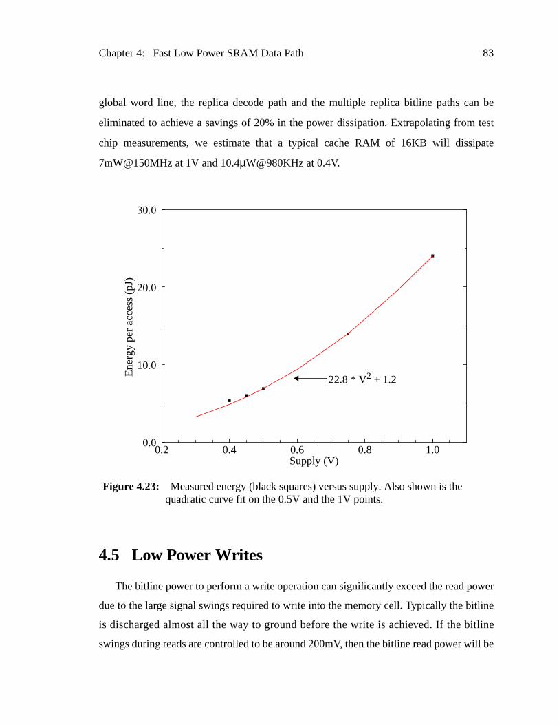
Chapter 4: Fast Low Power SRAM Data Path 83
n be
test
ate
wer
line
tline
ill be
global word line, the replica decode path and the multiple replica bitline paths ca
eliminated to achieve a savings of 20% in the power dissipation. Extrapolating from
chip measurements, we estimate that a typical cache RAM of 16KB will dissip
7mW@150MHz at 1V and 10.4µW@980KHz at 0.4V.
4.5 Low Power Writes
The bitline power to perform a write operation can significantly exceed the read po
due to the large signal swings required to write into the memory cell. Typically the bit
is discharged almost all the way to ground before the write is achieved. If the bi
swings during reads are controlled to be around 200mV, then the bitline read power w
0.2 0.4 0.6 0.8 1.0Supply (V)
0.0
10.0
20.0
30.0
Ene
rgy
per
acce
ss (
pJ)
22.8 * V2 + 1.2
Figure 4.23: Measured energy (black squares) versus supply. Also shown is thequadratic curve fit on the 0.5V and the 1V points.
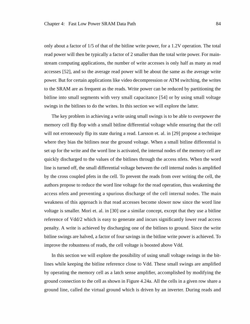
Chapter 4: Fast Low Power SRAM Data Path 84
tal
ain-
s read
e write
ites
g the
age
r the
ell
ique
ial is
ll are
word
ified
l, the
ng the
main
rd line
itline
cess
rite
. To
it-
lified
g the
are a
and
only about a factor of 1/5 of that of the bitline write power, for a 1.2V operation. The to
read power will then be typically a factor of 2 smaller than the total write power. For m
stream computing applications, the number of write accesses is only half as many a
accesses [52], and so the average read power will be about the same as the averag
power. But for certain applications like video decompression or ATM switching, the wr
to the SRAM are as frequent as the reads. Write power can be reduced by partitionin
bitline into small segments with very small capacitance [54] or by using small volt
swings in the bitlines to do the writes. In this section we will explore the latter.
The key problem in achieving a write using small swings is to be able to overpowe
memory cell flip flop with a small bitline differential voltage while ensuring that the c
will not erroneously flip its state during a read. Larsson et. al. in [29] propose a techn
where they bias the bitlines near the ground voltage. When a small bitline different
set up for the write and the word line is activated, the internal nodes of the memory ce
quickly discharged to the values of the bitlines through the access nfets. When the
line is turned off, the small differential voltage between the cell internal nodes is ampl
by the cross coupled pfets in the cell. To prevent the reads from over writing the cel
authors propose to reduce the word line voltage for the read operation, thus weakeni
access nfets and preventing a spurious discharge of the cell internal nodes. The
weakness of this approach is that read accesses become slower now since the wo
voltage is smaller. Mori et. al. in [30] use a similar concept, except that they use a b
reference of Vdd/2 which is easy to generate and incurs significantly lower read ac
penalty. A write is achieved by discharging one of the bitlines to ground. Since the w
bitline swings are halved, a factor of four savings in the bitline write power is achieved
improve the robustness of reads, the cell voltage is boosted above Vdd.
In this section we will explore the possibility of using small voltage swings in the b
lines while keeping the bitline reference close to Vdd. These small swings are amp
by operating the memory cell as a latch sense amplifier, accomplished by modifyin
ground connection to the cell as shown in Figure 4.24a. All the cells in a given row sh
ground line, called the virtual ground which is driven by an inverter. During reads
Chapter 4: Fast Low Power SRAM Data Path 85
ional
f the
ord
rnal
l to
high
a full
ber of
t the
standby, the virtual ground is driven low, and the SRAM operates as in the convent
case. During writes, the virtual ground line is first driven high to reset the contents o
cells. The write data is put onto the bitlines in the form of small voltage swings. The w
line is pulsed high and the small swing bitline signal is the transferred into the inte
nodes of the cell after which the virtual ground line is driven low, causing the cel
amplify and latch the data. Since the cell access transistors are nfets, the word line
voltage needs to be at least an nMOS threshold above bitline high voltage, to enable
reset of the cell (see waveform schematics in Figure 4.24b). Thus instead of a num
bitlines swinging full rail, this scheme enables all of them to have only small swings a
expense of an additional full swing line in the word line direction.
gwl
bs bsw
vgnd
wl
Vboost
b0 b0 bk bk
a)
wl
vgnd
b, b
Read access Write accessb)
Vboost
VG
Figure 4.24: a) Schematic of cells for low swing writes b) waveforms
Chapter 4: Fast Low Power SRAM Data Path 86
used,
e dur-
o be
d line
d cell
the
drop
the
n also
rea of
rtially
e bit-
rtual
be
han
heir
pro-
sired
.
ord
se to
om to
ll and
e word
age of
hence
There are a couple of limitations to this approach. Since boosted word lines are
the access nfets will have a higher current drive which also makes the cell less stabl
ing reads. To achieve a robust cell, either the pull down nfets within the cell have t
increased in size, the supply voltage to the cell should also be boosted, or the wor
voltage should not be boosted for reads. A more significant problem is that the rea
currents from all the accessed cells in a row flow through the pull down device of
inverter VG, causing the virtual ground line, vgnd, to have a small voltage drop. This
needs to be limited by carefully sizing the pull down device in VG, to ensure that
memory cells have sufficient read noise margins. This extra ground resistance ca
slow down the read access since the read cell currents will be reduced. Also, the a
the word driver increases because of the extra inverter. But this area increase is pa
offset by a reduction in the area for the write drivers and the precharge devices for th
lines as the write swing is reduced.
One limitation of the approach is that since the cells along a word line share the vi
ground line, all of these will get over written. This implies that the block width needs to
the same as the write word width. In order to allow for write widths which are smaller t
the block width, the write operation can be modified to first read the cell to transfer t
data on the bitlines, and then writing new data onto the desired subset of bitlines and
ceeding with the write as above. Thus though all the cells are over written, only the de
subset is written with the new data while the rest are over written with their own data
Another limitation of the approach is the requirement of boosted voltage for the w
lines during writes. High performance SRAMs are already operated with supplies clo
the upper limit prescribed for the process and there might not be any more head ro
boost the voltages further. An alternative will be to use pfet access devices in the ce
use a negative going word line. This approach also has the advantage that the sam
line voltage of 0 can be used for both the reads and the writes. The main disadvant
this approach is that the pfets are about a factor of three slower than the nfets and
the reads become slower.
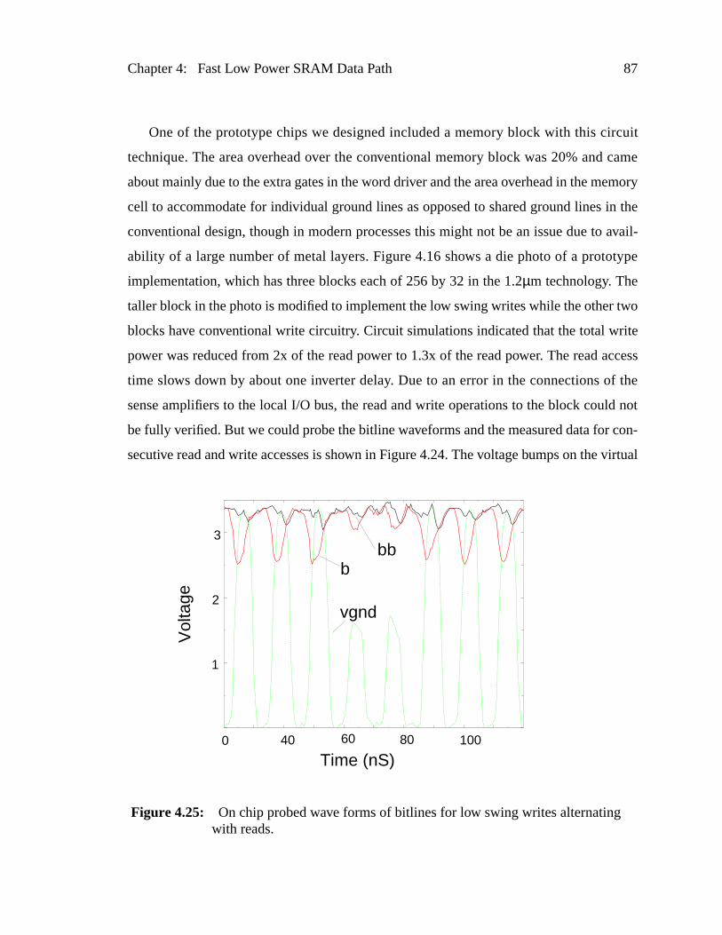
Chapter 4: Fast Low Power SRAM Data Path 87
cuit
came
emory
in the
avail-
type
wo
rite
ccess
f the
d not
con-
virtual
One of the prototype chips we designed included a memory block with this cir
technique. The area overhead over the conventional memory block was 20% and
about mainly due to the extra gates in the word driver and the area overhead in the m
cell to accommodate for individual ground lines as opposed to shared ground lines
conventional design, though in modern processes this might not be an issue due to
ability of a large number of metal layers. Figure 4.16 shows a die photo of a proto
implementation, which has three blocks each of 256 by 32 in the 1.2µm technology. The
taller block in the photo is modified to implement the low swing writes while the other t
blocks have conventional write circuitry. Circuit simulations indicated that the total w
power was reduced from 2x of the read power to 1.3x of the read power. The read a
time slows down by about one inverter delay. Due to an error in the connections o
sense amplifiers to the local I/O bus, the read and write operations to the block coul
be fully verified. But we could probe the bitline waveforms and the measured data for
secutive read and write accesses is shown in Figure 4.24. The voltage bumps on the
0 40 60 80 100
1
2
3
Time (nS)
Vol
tage
vgnd
bbb
Figure 4.25: On chip probed wave forms of bitlines for low swing writes alternatingwith reads.

Chapter 4: Fast Low Power SRAM Data Path 88
evice
vice
area
proach
rite
ance
tial for
ed for
ines
ct
nsists
mory
the
strated.
d and
s the
and
. The
ce as
t the
write
The
sense
This
ground node is about 1.5V during the read access indicating that the pull down d
width connected to this line is not sufficiently wide. For reliable read operations the de
width needs to be increased by a factor of four, which in turn will increase the total
overhead by an additional 5%. The area and read access penalty inherent in this ap
might not be acceptable to a large number of applications in return for the lower w
power.
4.6 Summary
The key to low power operation is to reduce the signal swings in the high capacit
nodes like the bitlines and the data lines. Clocked voltage sense amplifiers are essen
obtaining low sensing power, and accurate generation of their sense clock is requir
high speed operation. An energy efficient way to obtain low voltage swings in the bitl
is to limit the word line pulse width, by controlling the pulse width of the block sele
signal. The pulse widths are regulated by the aid of a replica delay element which co
of a replica memory cell and a replica bitline and hence tracks the delay of the me
cell over a wide range of process and operating conditions. Two variations of
technique were discussed and their use to generate the sense clock was also demon
We believe that this is a very simple and robust technique with very low area overhea
is easily applicable to a wide variety of SRAM designs. The chapter also demonstrate
application of the technique to achieve low swing data line operation for both the read
write accesses, by pulsing the control signal which gates the drivers of these lines
pulse width is controlled by discharging a replica line which has the same capacitan
the worst case data line. This replica line is also used to trigger the amplifiers a
receiving end of these lines. Finally we presented a technique to achieve low bitline
power, by using small voltage swings on the bitlines during the write operation.
memory cell structure is modified such that the cells can be used as latch type
amplifier to amplify and store the small swing write data presented on the bitlines.

Chapter 4: Fast Low Power SRAM Data Path 89
nly for
and
and
er by
technique requires boosted word lines and 20% larger area and hence is suitable o
certain niche applications.
In the next chapter we will take a step back from detailed circuit design issues
look at scaling trends of delay and power in SRAMs as a function of their size
technology. We will assume that the SRAMs have been optimized for speed and pow
using some of the techniques discussed in this chapter.
Chapter 4: Fast Low Power SRAM Data Path 90
Chapter
hnol-
AM.
d be
Such
used
by a
lop
vari-
models
his
area
on-
evel
onal
then
differ-
: the
d mis-
pects
5 Speed and PowerScaling of SRAMs
This chapter analyzes the scaling of delay and power of SRAMs with size and tec
ogy using some simple analytical models for the various components of the SR
Exploring the large design space using conventional SPICE circuit simulation woul
extremely time consuming and hence simplified analytical models are very valuable.
models not only help in designing SRAMs for the current generation, but can also be
to forecast future trends.
Analytical models for delay, area and energy have been developed separately
number of authors [56-59]. Wada et. al. in [56] and Wilton and Jouppi in [57], deve
delay models for the decoder and the bitline path and use it to explore the impact of
ous cache organizations on the access time. Evans and Franzon develop analytical
in [58-59] for the energy consumption of an SRAM as a function of its organization. T
chapter extends the delay models of [56] and combines them with the energy and
models for the SRAM. The delay models are modified to include the effects of interc
nect resistance and more complex partitioning schemes. We allow for multi-l
hierarchical structures for the bitline and data line muxes [54, 60], which is an additi
degree of freedom in the organization not considered by [56-59]. The models are
used to estimate the delay, area and energy of SRAMs of various capacities and in
ent technology generations.
With feature size shrinking by a factor of 2 every 18 months, two effects stand out
interconnect delay is getting worse compared to the transistor delay and the threshol
matches between transistors are not scaling with the supply voltage [61-62]. One ex
91
Chapter 5: Speed and Power Scaling of SRAMs 92
nfor-
ithin
esti-
the
amin-
n 5.1
make
nsive
s we
. We
te the
er of
ing a
to 4
essed
and
und-
e next
both these effects to have a significant influence on SRAMs, since SRAMs require i
mation to be broadcast globally across the whole array and part of the signal path w
the array uses small signal swings followed by sense amplification. The chapter inv
gates both these effects with the aid of the analytical models.
As explained in Chapter 2, a lot of attention is paid to organizing and partitioning
cell array to manage the delay and power. Hence our analysis incorporates this by ex
ing a large number of different organizations to determine the optimal ones. Sectio
explains our notation for capturing each partition. To keep the analysis tractable, we
certain simplifying assumptions and discuss the main ones in Section 5.2. An exte
list of all the other assumptions is provided in Appendix C. Using these assumption
then develop models for delay, area and energy for the key components of the SRAM
then apply these models to estimate the delay and power for SRAMs and investiga
scaling trends with densities and technology in Section 5.3.
5.1 SRAM Partitioning
At the top level, any partitioning can be captured by three variables: the numb
macros (nm) which comprise the array, the block width (bw) and block height (bh) of each
of the sub blocks which make up a macro. Figure 5.1 shows an example of partition
1024x1024 array of cells of a 1Mb SRAM for a 64 bit access. The array is broken in
macros all of which are accessed simultaneously, each providing 16 bits of the acc
word. Each macro is further subdivided into four blocks of 512 rows and 128 columns
with one of the blocks furnishing the 16 bit sub word.
As discussed in Chapter 2, partitioning of the RAM incurs area overhead at the bo
aries of the partitions. Hence we estimate area as an integral part of the analysis. Th

Chapter 5: Speed and Power Scaling of SRAMs 93
lay and
some
e key
dis-
coder
ower
section details the assumptions made for the analysis and describes the area, de
power models developed for the RAM.
5.2 Modeling of the SRAM
In order to explore the large SRAM design space in a tractable manner, we make
simplifying assumptions about certain aspects of the design. We outline and justify th
assumptions in the next sub section and list all the assumptions in Appendix C. As
cussed in Chapter 2, the SRAM path can be broken into two components, the row de
and the RAM data path. We develop simple analytical models for delay, area and p
for these and the verify these against HSPICE circuit simulations.
deco
der
16
64
bw=128 cells
bh=512
nm = 4
nm = number of macros
bh = block height
bw = block width
cells
Figure 5.1: Array partitioning example
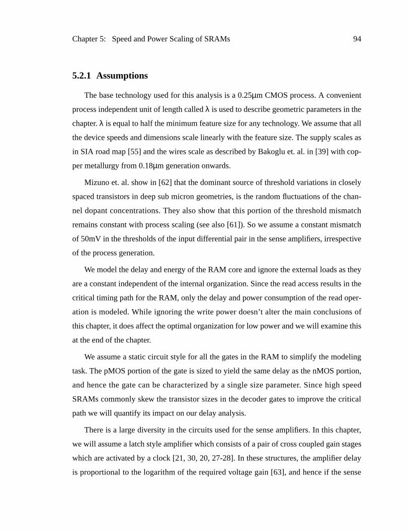
Chapter 5: Speed and Power Scaling of SRAMs 94
t
he
t all
ales as
cop-
sely
chan-
atch
smatch
ctive
they
s in the
per-
s of
this
ling
rtion,
speed
itical
pter,
tages
elay
ense
5.2.1 Assumptions
The base technology used for this analysis is a 0.25µm CMOS process. A convenien
process independent unit of length calledλ is used to describe geometric parameters in t
chapter.λ is equal to half the minimum feature size for any technology. We assume tha
the device speeds and dimensions scale linearly with the feature size. The supply sc
in SIA road map [55] and the wires scale as described by Bakoglu et. al. in [39] with
per metallurgy from 0.18µm generation onwards.
Mizuno et. al. show in [62] that the dominant source of threshold variations in clo
spaced transistors in deep sub micron geometries, is the random fluctuations of the
nel dopant concentrations. They also show that this portion of the threshold mism
remains constant with process scaling (see also [61]). So we assume a constant mi
of 50mV in the thresholds of the input differential pair in the sense amplifiers, irrespe
of the process generation.
We model the delay and energy of the RAM core and ignore the external loads as
are a constant independent of the internal organization. Since the read access result
critical timing path for the RAM, only the delay and power consumption of the read o
ation is modeled. While ignoring the write power doesn’t alter the main conclusion
this chapter, it does affect the optimal organization for low power and we will examine
at the end of the chapter.
We assume a static circuit style for all the gates in the RAM to simplify the mode
task. The pMOS portion of the gate is sized to yield the same delay as the nMOS po
and hence the gate can be characterized by a single size parameter. Since high
SRAMs commonly skew the transistor sizes in the decoder gates to improve the cr
path we will quantify its impact on our delay analysis.
There is a large diversity in the circuits used for the sense amplifiers. In this cha
we will assume a latch style amplifier which consists of a pair of cross coupled gain s
which are activated by a clock [21, 30, 20, 27-28]. In these structures, the amplifier d
is proportional to the logarithm of the required voltage gain [63], and hence if the s

Chapter 5: Speed and Power Scaling of SRAMs 95
con-
ense
ck
een
spe-
has
outed
s is
hap-
t of a
cant.
ption
tions
wires.
wer
ances
the
1a,b
to the
n
and
clock timing is well controlled, they lead to the fastest implementations. They also
sume very low power since they are inherently clocked. We will assume that the s
clock timing is perfectly controlled but will quantify the impact of non ideal sense clo
generation on our delay estimates.
When the number of wiring levels is limited, space has to be allocated in betw
blocks to route the data lines. This significantly adds to the overall memory area, e
cially when the block size is very small. Since the number of available wiring levels
been steadily growing [55], we will assume in this chapter that the data lines can be r
vertically over the array if required. Thus extra routing space for a horizontal bu
required only once at the bottom of the array.
Transistor sizing offers another technique to trade-off delay, area and power. In C
ter 3 we found that for high speed designs, sizing each gate to yield a delay of tha
fanout of 4 loaded inverter works pretty well as long as the wire delays are not signifi
We assume this sizing rule in this chapter to simplify the analysis. While this assum
does not affect minimum delay solutions, it causes the low energy and low area solu
to be sub optimal and we examine this further at the end of the chapter.
We use the simple RC models of Chapter 3 to model the delay of the gates and the
In an energy efficient SRAM design, the dynamic power dominates the total po
dissipation, and so we only model the dynamic energy required to switch the capacit
in the decoder and the output mux. We will next discuss in detail the models for
decoder and the output mux.
5.2.2 Decoder model
The decoder delay with the fanout of 4 sizing rule is summarized in Equations
and is the sum of the extrinsic delays of each gate in the path (each of which is equal
extrinsic delay of the fanout 4 inverter,τfo4x), their intrinsic delays and the wire delays. I
these equationsN is the number of gates in the path,pi is the parasitic delay of gatei, G is
the gate loading due to all the global word drivers connected to the predecode wireL

Chapter 5: Speed and Power Scaling of SRAMs 96
the
RC
rate
1.4
n 2.
um of
ate of
d glo-
word
qua-
eas
th
area
izing
ires is
width
is the gate loading of all the local word drivers connected to a global word line. Since
local and global word lines are driven from their center by their respective drivers, the
delay of these wires is reduced by a factor of 4.
Since bitline delay depends on the local word line rise time, we estimate the edge
at the end of the local word line. From circuit simulations the rise time was found to be
times the delay of the final stage of the word driver and is summarized in Equatio
Since the final stage is sized to have a fanout of 4, the total delay of the stage is the s
a fanout of 4 inverter delay (τfo4) and the RC delay of the local word line (rwl * cwl / 8
assuming that the word drivers drive the local word line from the center of the line).
The gate and wire capacitances in the signal path are added up to give an estim
the decoder energy. Decoder area is calculated by estimating the area of the local an
bal word drivers and the area required for the predecode wires. The area of the
drivers is modeled as a linear function of the total device widths inside the drivers (E
tion 3). The constants for this function have been obtained by fitting it to the ar
obtained from the layout of six different word drivers [28, 30]. The total device wid
within the driver is estimated to be 1.25 times the size of the final buffer as the active
of the pre driver can approximated to be a quarter of the final inverter when fanout 4 s
is used for the gates. The area for running the vertical predecode and block select w
also added to the total decode area. As an example, the increase in the SRAM array
Ddecoder N τ fo4x⋅ pii 0=
N
∑ Dwire+ +=
Dwire r p cp 2⁄ G+( ) rg cg L+( ) 8⁄ rwl cwl 8⁄⋅+⋅+⋅= (1b)
(1a)
τ fo4 rwl cwl 8⁄⋅+( ) 1.4×= (2)rise time
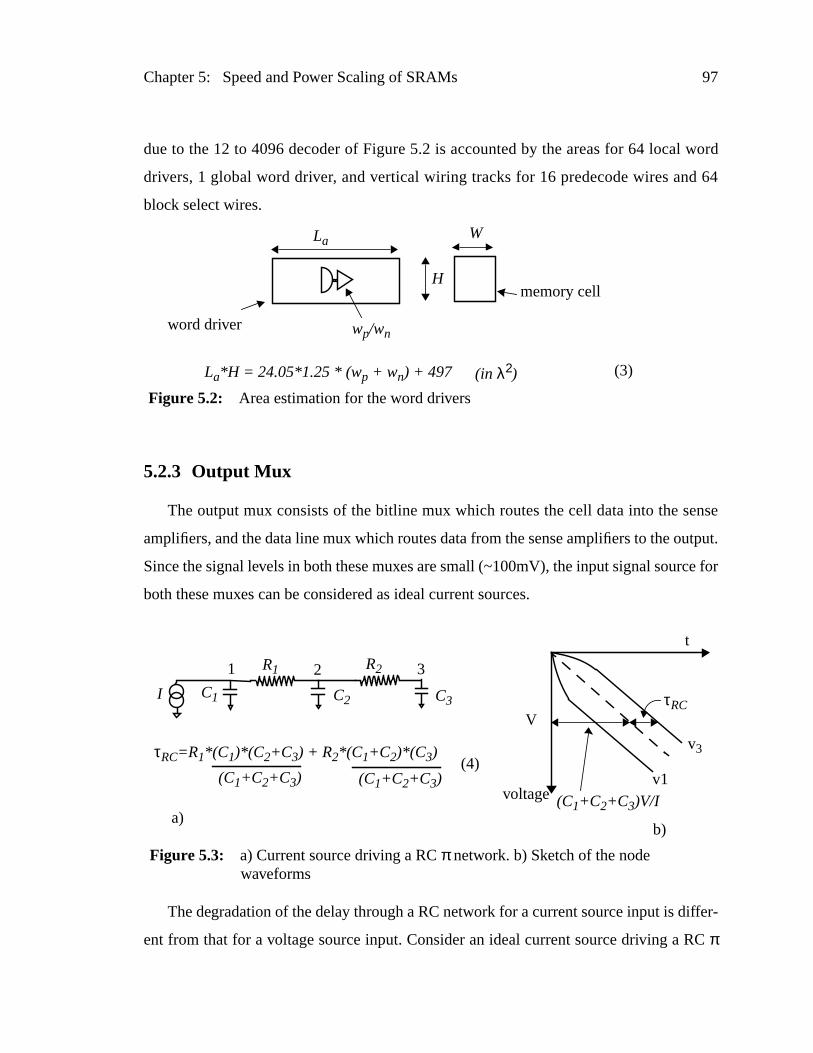
Chapter 5: Speed and Power Scaling of SRAMs 97
word
64
ense
utput.
ce for
iffer-
C
due to the 12 to 4096 decoder of Figure 5.2 is accounted by the areas for 64 local
drivers, 1 global word driver, and vertical wiring tracks for 16 predecode wires and
block select wires.
5.2.3 Output Mux
The output mux consists of the bitline mux which routes the cell data into the s
amplifiers, and the data line mux which routes data from the sense amplifiers to the o
Since the signal levels in both these muxes are small (~100mV), the input signal sour
both these muxes can be considered as ideal current sources.
The degradation of the delay through a RC network for a current source input is d
ent from that for a voltage source input. Consider an ideal current source driving a Rπ
La W
H
wp/wn
La*H = 24.05*1.25 * (wp + wn) + 497
memory cell
word driver
(3)(in λ2)
Figure 5.2: Area estimation for the word drivers
I C1 C2
R11 2
t
voltagev1
v3
V
(C1+C2+C3)V/I
τRC
a)b)
C3
R2 3
τRC=R1*(C1)*(C2+C3) + R2*(C1+C2)*(C3)
(C1+C2+C3) (C1+C2+C3)(4)
Figure 5.3: a) Current source driving a RCπ network. b) Sketch of the nodewaveforms
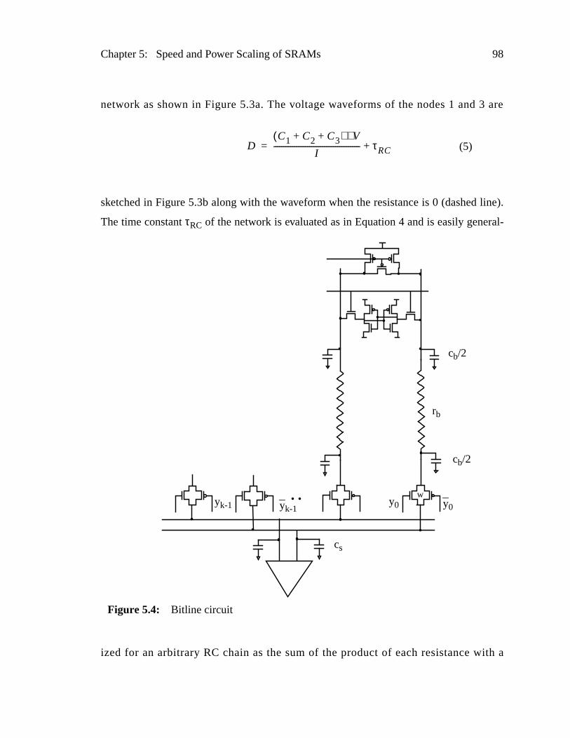
Chapter 5: Speed and Power Scaling of SRAMs 98
are
line).
ral-
ith a
network as shown in Figure 5.3a. The voltage waveforms of the nodes 1 and 3
sketched in Figure 5.3b along with the waveform when the resistance is 0 (dashed
The time constantτRC of the network is evaluated as in Equation 4 and is easily gene
ized for an arbitrary RC chain as the sum of the product of each resistance w
DC1 C2 C3+ +( ) V⋅
I---------------------------------------------- τRC+= (5)
y0y0yk-1yk-1
rb
cb/2
cb/2
w
cs
Figure 5.4: Bitline circuit
Chapter 5: Speed and Power Scaling of SRAMs 99
mped
e (t >>
ode 3
us the
bit-
rent
mux
lay to
ge
local
time
time
por-
d
ula-
capacitance which is obtained by considering all the downstream capacitance lu
together, in series with all the upstream capacitance lumped together. In steady stat
τRC), nodes 1, 2 and 3 slew at the same rate, and the delay to obtain a swing of V at n
can be approximated by Equation 5, which is the delay when there is no resistance pl
time constant of the network. This formula is used for estimating the delay of both the
line and data line muxes.
A single level bitline mux is shown in Figure 5.4 and is modeled as an ideal cur
source driving a RC network as in Figure 5.3. Local and global bitline wires and the
switches contribute to the capacitances and resistances in the network. The bitline de
obtain a signal swing ofδv by Equation 7 is the sum of the delay to generate the volta
swing with no resistance and the time constant of the RC network (Equation 6). Long
word lines can have slow rise times because of the line resistance. Since the rise
affects the cell delay, we need to include it in the delay model. The effect of the rise
(Tr) can be captured by adding an additional term to the delay equation which is pro
tional to it [57]. The proportionality constant,α, depends on the ratio of the threshol
voltage of the access device in the cell, to the supply voltage and we find it from sim
tions to be about 0.3 for a wide range of block widths. The RC time constant,τRC, in the
Db cb jmux k 1+( ) cs+⋅+( ) δvI cell----------⋅ α Tr⋅ τRC+ += (6)
cb: Bitline capacitance
jmux: Unit junction capacitance of the mux switch
k: Number of columns multiplexed into a single sense amplifiercs: Input capacitance of the sense amplifier
δv: Voltage swing at the input of the sense amplifierIcell: Memory cell current
Tr: Local word line rise time
α: Proportionality constant determined from HSPICEτRC: Time constant of the bitline RC network
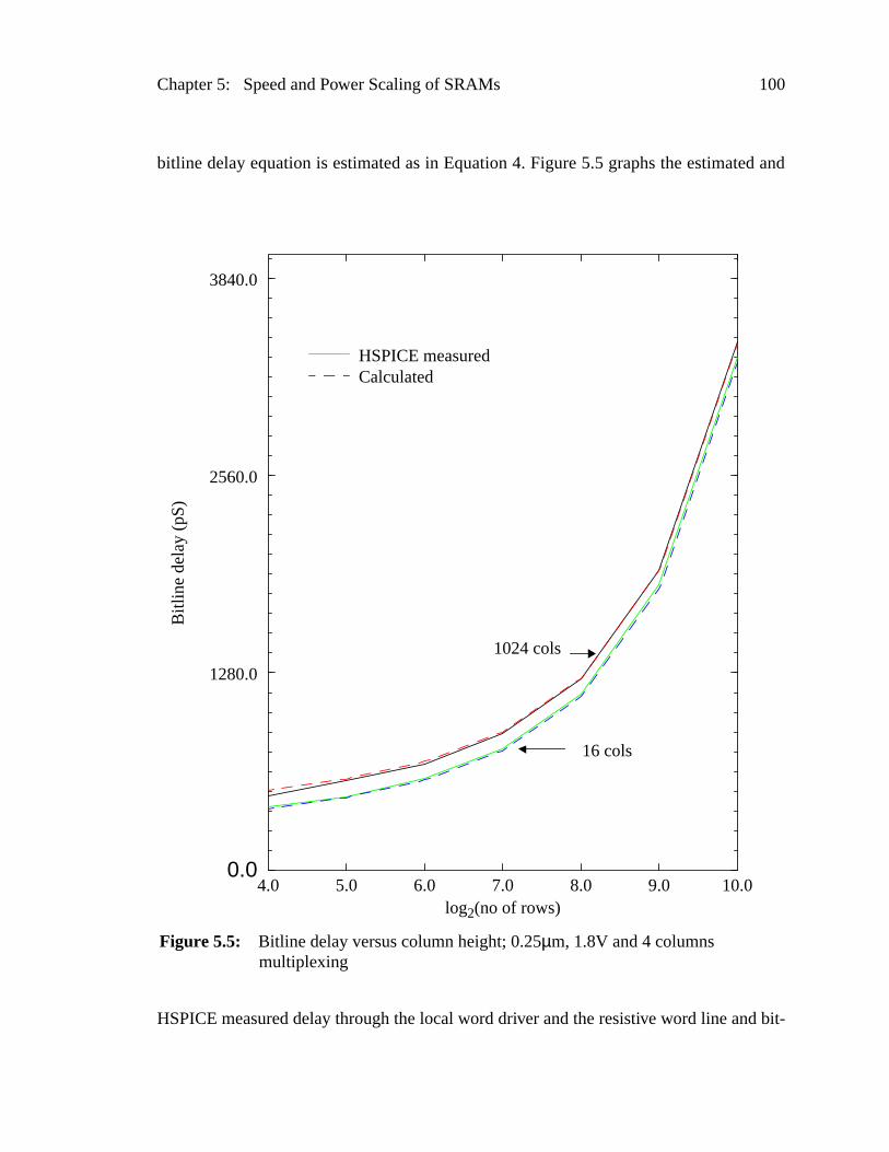
Chapter 5: Speed and Power Scaling of SRAMs 100
d and
d bit-
bitline delay equation is estimated as in Equation 4. Figure 5.5 graphs the estimate
HSPICE measured delay through the local word driver and the resistive word line an
4.0 5.0 6.0 7.0 8.0 9.0 10.0log2(no of rows)
0.0
1280.0
2560.0
3840.0
Bitl
ine
dela
y (p
S)
HSPICE measuredCalculated
1024 cols
16 cols
Figure 5.5: Bitline delay versus column height; 0.25µm, 1.8V and 4 columnsmultiplexing
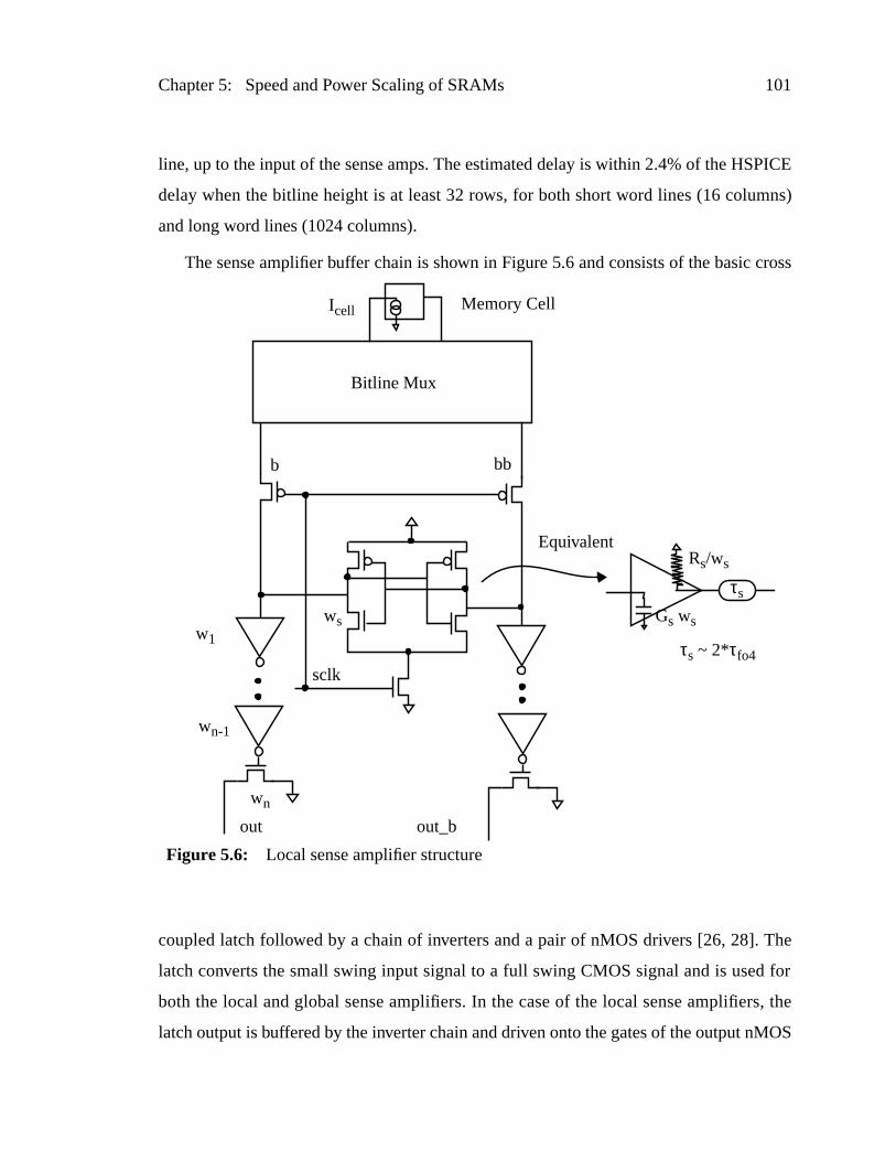
Chapter 5: Speed and Power Scaling of SRAMs 101
PICE
ns)
cross
The
for
s, the
MOS
line, up to the input of the sense amps. The estimated delay is within 2.4% of the HS
delay when the bitline height is at least 32 rows, for both short word lines (16 colum
and long word lines (1024 columns).
The sense amplifier buffer chain is shown in Figure 5.6 and consists of the basic
coupled latch followed by a chain of inverters and a pair of nMOS drivers [26, 28].
latch converts the small swing input signal to a full swing CMOS signal and is used
both the local and global sense amplifiers. In the case of the local sense amplifier
latch output is buffered by the inverter chain and driven onto the gates of the output n
b bb
sclk
out out_b
w1
wn-1
wn
ws Gs ws
Rs/ws
τs
Equivalent
τs ~ 2*τfo4
Bitline Mux
Icell Memory Cell
Figure 5.6: Local sense amplifier structure
Chapter 5: Speed and Power Scaling of SRAMs 102
ts by
rging
delay
. For
f the
itance
latch,
their
evant
f the
sim-
erter
drivers. These nMOS transistors create a small swing voltage signal at their outpu
discharging a previously precharged data lines (analogous to the memory cell discha
the precharged bitlines). The delay of the sense amplifier structure is the sum of the
of the latch amplifier,τs, and the delay to buffer and drive the outputs.τs is proportional to
the logarithm of the desired voltage gain and the loading of the amplifier outputs [63]
a gain of about 20 with only the self loading of the amplifier,τs is found to be about 2τfo4
by both calculations and circuit simulations. If we assume that all the transistors o
latch are scaled in the same proportion, then its output resistance and input capac
can be expressed as simple functions of the size of the cross coupled nMOS in the
ws, as shown in Figure 5.6. The nMOS drivers are modeled as current sources, with
current output proportional to their sizewn. As in the decoders, optimal sizesws, w1,.. wn
are determined to minimize the total output mux delay. Equation 7 captures the rel
portions of the output mux delay needed for doing this optimization, and is the sum o
delays of the bitline mux, the latch sense amp, the buffers and the nMOS drivers. To
T Db ws( ) τs
Rs 3 Cg w1⋅ ⋅ ⋅ws
------------------------------------Rg 3 Cg w2⋅ ⋅ ⋅
w1------------------------------------+ + +=
Rg Cg wn⋅ ⋅wn 1–
----------------------------- C δv⋅I n wn⋅----------------+ (7). . .
Gs = 3.8fF/λ: sense amp input capacitance per unit width in 0.25µm process
Rs = 36kΩ-λ: sense amp output resistance per unit width
ws: size of sense amp
Rg, Cg: output resistance and input capacitance per unit width of a 2:1 inv
In = 37.5µA/λ: current per unit width of nMOS
C: Capacitance of the data line mux
Db ws( )Gs ws δv⋅ ⋅
I cell---------------------------≈ (8)
τs = 2τfo4; amplification delay of the latch sense amp
+ other constants

Chapter 5: Speed and Power Scaling of SRAMs 103
n the
n 8).
time
lude
cture
aded
t that
lifier
. This
tech-
d the
lsing
e and
d
plify the procedure for finding the optimal sizes, impact of the latch sense amp size o
bitline mux time constant is ignored and only the cell delay is considered (Equatio
Similarly, we ignore the effect of the nMOS junction capacitance on the data line RC
constant. Both these factors have little influence on the optimal sizing, but we inc
them for the final delay calculations. The minimum delay through the sense amp stru
occurs when each term in Equation 7 is equal to the extrinsic delay of a fanout of 4 lo
inverter. The delay of the global sense amp is estimated in a similar fashion, excep
the buffering delay to drive the output load is not considered in this analysis.
With technology scaling if the transistor threshold mismatch in the sense amp
doesn’t scale, then the delay of the output mux has a component which doesn’t scale
component is the delay of the memory cell to generate the bitline swing ofδvm, which is
the input offset voltage of the sense amplifier. Hence for delay estimations in future
nologies, we keep this component a constant.
For low power operation the signals on high capacitance nodes like the bitlines an
data lines are clamped to have small voltage swings [28]. Bitlines are clamped by pu
the word lines, resulting in a total signal swing of about 2 *δv (the data lines are clamped
in an analogous fashion to have similar signal swings). Hence the energy of the bitlin
data line mux is computed as C *Vdd * 2 * δv, where C is the capacitance on the line an
includes the wire, junction and input gate capacitances and Vdd is the supply voltage. The
energy of a unit sized sense amp is obtained from simulations to be 12fJ/λ for the 0.25µm
process and it is scaled up byws to obtain the sense amp energy.
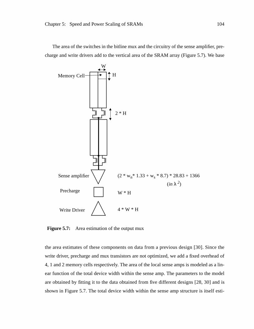
Chapter 5: Speed and Power Scaling of SRAMs 104
pre-
base
ce the
ad of
s a lin-
odel
d is
esti-
The area of the switches in the bitline mux and the circuitry of the sense amplifier,
charge and write drivers add to the vertical area of the SRAM array (Figure 5.7). We
the area estimates of these components on data from a previous design [30]. Sin
write driver, precharge and mux transistors are not optimized, we add a fixed overhe
4, 1 and 2 memory cells respectively. The area of the local sense amps is modeled a
ear function of the total device width within the sense amp. The parameters to the m
are obtained by fitting it to the data obtained from five different designs [28, 30] an
shown in Figure 5.7. The total device width within the sense amp structure is itself
Sense amplifier
Precharge
Write Driver
2 * H
W * H
4 * W * H
(2 * wn* 1.33 + ws * 8.7) * 28.83 + 1366
W
HMemory Cell
(in λ 2)
Figure 5.7: Area estimation of the output mux

Chapter 5: Speed and Power Scaling of SRAMs 105
in
tput
-
any
rgy of
opti-
ergy
eight
ess
-
as
output
t equal
elects
here S
s in
mated from the size parametersws,wn & wp. The sum of all the device widths within the
latch is estimated asws * 8.7, where the factor of 8.7 is obtained for the latch design
[30]. With fanout of 4 sizing, the active area of the buffers prior to each nMOS ou
driver is no more than 1/3 of the driver widthwn. Hence the active area of two nMOS driv
ers and their respective buffers is given by 2 *wn * 1.33.
We will next describe the results obtained by using these models to analyze m
RAM organizations of different sizes in various technology generations.
5.3 Analysis Results
We enumerate all the RAM organizations and estimate the area, delay and ene
each using the simple models described previously. This allows us to determine the
mal organizations which minimize a weighted objective function of delay, area and en
(Equation 9). The trade-off curves are also obtained between these, by varying the w
valuesα andβ between 0 and 1.
Figure 5.8 plots the delay of SRAMs organized for minimum delay (α = β = 0 in
Equation 7), with and without wire resistance, for sizes from 64Kb to 16Mb with acc
width of 64 bits, in the 0.25µm technology. The delay of the SRAM without wire resis
tance, is about 15τfo4 for a 64Kb design, and is proportional to the log of the capacity
observed in [56]. The delay increases by about 1.2τfo4 for every doubling of the RAM
size and can be understood in terms of the delay scaling of the row decoder and the
path. The delays for both of these are also plotted in the same graph and are almos
in an optimally organized SRAM. In the case of the row decoder, each address bit s
half the array, and hence the loading seen by the address bit is proportional to S/2, w
is the total number of bits in the array. With fanout 4 sizing rule, the number of stage
1 β α––( ) Delay⋅ α Area⋅ β Energy⋅+ + (9)minimize[over all partitions]
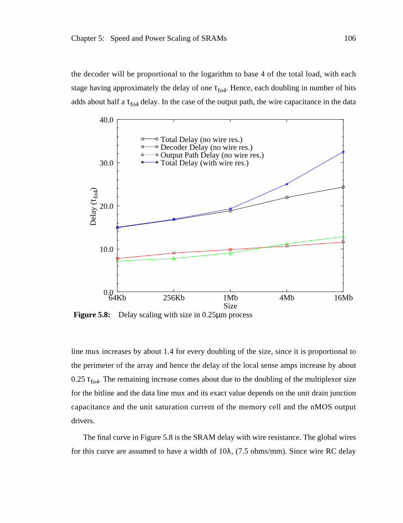
Chapter 5: Speed and Power Scaling of SRAMs 106
ach
s
data
al to
about
size
ction
utput
ires
the decoder will be proportional to the logarithm to base 4 of the total load, with e
stage having approximately the delay of oneτfo4. Hence, each doubling in number of bit
adds about half aτfo4 delay. In the case of the output path, the wire capacitance in the
line mux increases by about 1.4 for every doubling of the size, since it is proportion
the perimeter of the array and hence the delay of the local sense amps increase by
0.25τfo4. The remaining increase comes about due to the doubling of the multiplexor
for the bitline and the data line mux and its exact value depends on the unit drain jun
capacitance and the unit saturation current of the memory cell and the nMOS o
drivers.
The final curve in Figure 5.8 is the SRAM delay with wire resistance. The global w
for this curve are assumed to have a width of 10λ, (7.5 ohms/mm). Since wire RC delay
64Kb 256Kb 1Mb 4Mb 16MbSize
0.0
10.0
20.0
30.0
40.0
Del
ay (τ
fo4)
Total Delay (no wire res.)Decoder Delay (no wire res.)Output Path Delay (no wire res.)Total Delay (with wire res.)
Figure 5.8: Delay scaling with size in 0.25µm process
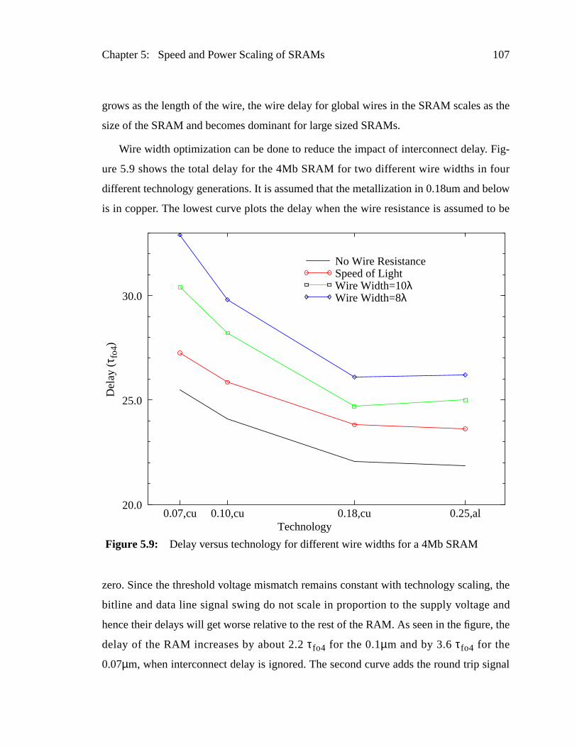
Chapter 5: Speed and Power Scaling of SRAMs 107
s the
Fig-
ur
elow
to be
g, the
and
, the
ignal
grows as the length of the wire, the wire delay for global wires in the SRAM scales a
size of the SRAM and becomes dominant for large sized SRAMs.
Wire width optimization can be done to reduce the impact of interconnect delay.
ure 5.9 shows the total delay for the 4Mb SRAM for two different wire widths in fo
different technology generations. It is assumed that the metallization in 0.18um and b
is in copper. The lowest curve plots the delay when the wire resistance is assumed
zero. Since the threshold voltage mismatch remains constant with technology scalin
bitline and data line signal swing do not scale in proportion to the supply voltage
hence their delays will get worse relative to the rest of the RAM. As seen in the figure
delay of the RAM increases by about 2.2τfo4 for the 0.1µm and by 3.6τfo4 for the
0.07µm, when interconnect delay is ignored. The second curve adds the round trip s
0.07,cu 0.10,cu 0.18,cu 0.25,al20.0
25.0
30.0
Del
ay (τ
fo4)
No Wire ResistanceSpeed of LightWire Width=10λWire Width=8λ
Technology
Figure 5.9: Delay versus technology for different wire widths for a 4Mb SRAM

Chapter 5: Speed and Power Scaling of SRAMs 108
S and
ay is
ery
nce
idth
ening
f
he
n be
ulti-
ta-
ally
takes
urves
ly
tes in
21],
ewed
When
64Kb
nd
lay
delays around the access path assuming a speed of light propagation of 1mm/6.6p
gives the lower bound for interconnect delay. The speed of light interconnect del
about 1.75τfo4 for the 4Mb SRAM, independent of the technology and doubles for ev
quadrupling of RAM size. The two curves above it graph the delay with wire resista
being non-zero for two different wire widths of 8λ and 10λ. Significant reduction in wire
delay is possible when fat wires are used for global wiring. Going from 0.25µm with alu-
minum wiring to 0.18µm copper wiring, essentially leaves the delays (in terms ofτfo4)
unchanged, but with further shrinks of the design, the delay for any particular wire w
worsens, since the wire RC delay doesn’t scale as well as the gate delay. But by wid
the wires in subsequent shrinks, it is possible to maintain the same delay (in terms oτfo4)
across process generations. A wire width of 10λ brings the delay within aτfo4 of speed of
light limit at the 0.25µm and 0.18µm generations, while wider wires are needed in t
0.1µm and 0.07µm generations. The larger pitch requirements for these fat wires ca
easily supported when the divided word line structure in the decoders and column m
plexing in the bitlines are used.
We will next look at some ways in which performance of actual SRAM implemen
tions might differ from those predicted by the previous curves. Large SRAMs typic
incorporate some form of row redundancy circuits in the decode path. This usually
the form of a series pass transistor in the local word driver and will cause the delay c
to shift up by about 1/2 to 1τfo4. Fanouts larger than 4 in the word line driver, common
done to reduce area, will also shift the delay curves up by about 1/2 to 1τfo4. High perfor-
mance SRAMs don’t use static circuit style in the entire decode path, but skew the ga
the predecoders and the global word drivers to favor a fast word line activation [20,
causing the delay curves to shift down. As discussed in Chapter 3, the delay of a sk
gate is about 70% that of a non skewed gate and grows slower with increasing load.
applied to the predecoder and the global word driver the delay of the decoder in the
RAM reduces to about 6τfo4 instead of the 8τfo4 for the static implementation leading to
a net decoder gain of up to 1τfo4 when combined with the losses due to redundancy a
smaller local word driver. But with every doubling of the RAM size, the decoder de
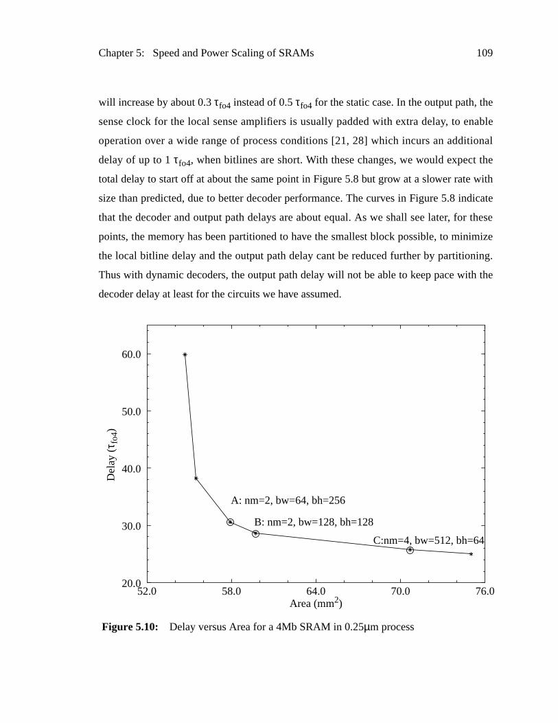
Chapter 5: Speed and Power Scaling of SRAMs 109
e
nable
onal
the
with
dicate
these
imize
ing.
h the
will increase by about 0.3τfo4 instead of 0.5τfo4 for the static case. In the output path, th
sense clock for the local sense amplifiers is usually padded with extra delay, to e
operation over a wide range of process conditions [21, 28] which incurs an additi
delay of up to 1τfo4, when bitlines are short. With these changes, we would expect
total delay to start off at about the same point in Figure 5.8 but grow at a slower rate
size than predicted, due to better decoder performance. The curves in Figure 5.8 in
that the decoder and output path delays are about equal. As we shall see later, for
points, the memory has been partitioned to have the smallest block possible, to min
the local bitline delay and the output path delay cant be reduced further by partition
Thus with dynamic decoders, the output path delay will not be able to keep pace wit
decoder delay at least for the circuits we have assumed.
52.0 58.0 64.0 70.0 76.0Area (mm2)
20.0
30.0
40.0
50.0
60.0
Del
ay (τ
fo4)
C:nm=4, bw=512, bh=64
B: nm=2, bw=128, bh=128
A: nm=2, bw=64, bh=256
Figure 5.10: Delay versus Area for a 4Mb SRAM in 0.25µm process

Chapter 5: Speed and Power Scaling of SRAMs 110
rves
AM
west
min-
a is
hile
a for
wn in
wer
red to
lock
5.11
imal
lay of
s due
lay
xam-
t 8%
Partitioning allows for a trade-off between delay, area, and power. Trade-off cu
can be obtained by solving Equation 9, with various values for the parametersα andβ.
Whenβ equals zero, the delay-area trade-off is obtained and the curve for a 4Mb SR
in 0.25µm process is shown in Figure 5.10. Any point on this curve represents the lo
area achievable via RAM reorganization for the corresponding delay. Starting from a
imum delay design which is finely partitioned, significant improvements in the are
possible by reducing the amount of partitioning and incurring a small delay penalty, w
subsequent reduction in partitioning results in decreasing improvements in are
increasing delay penalty. Partitioning parameters for three points A, B and C are sho
the figure. Points A & B are in the sweet spot of the curve, with A being about 22% slo
and 22% smaller area and B being 14% slower and 20% smaller area when compa
the fastest implementation.
Of the various organization parameters, the RAM delay is most sensitive to the b
height and fast access times are obtained by using smaller block heights. Figure
shows the delay and area for a 4Mb SRAM for various block heights, while using opt
values for the remaining organization parameters. Small block heights reduce the de
the bitlines, but increase the delay of the global wires since the RAM area is increase
to the overhead of bitline partitioning. For very large block heights, the slow bitline de
limits the access time. Hence an optimum block height exists and is 32 rows for the e
ple above. Increasing the block height to 128 rows incurs a delay penalty of abou
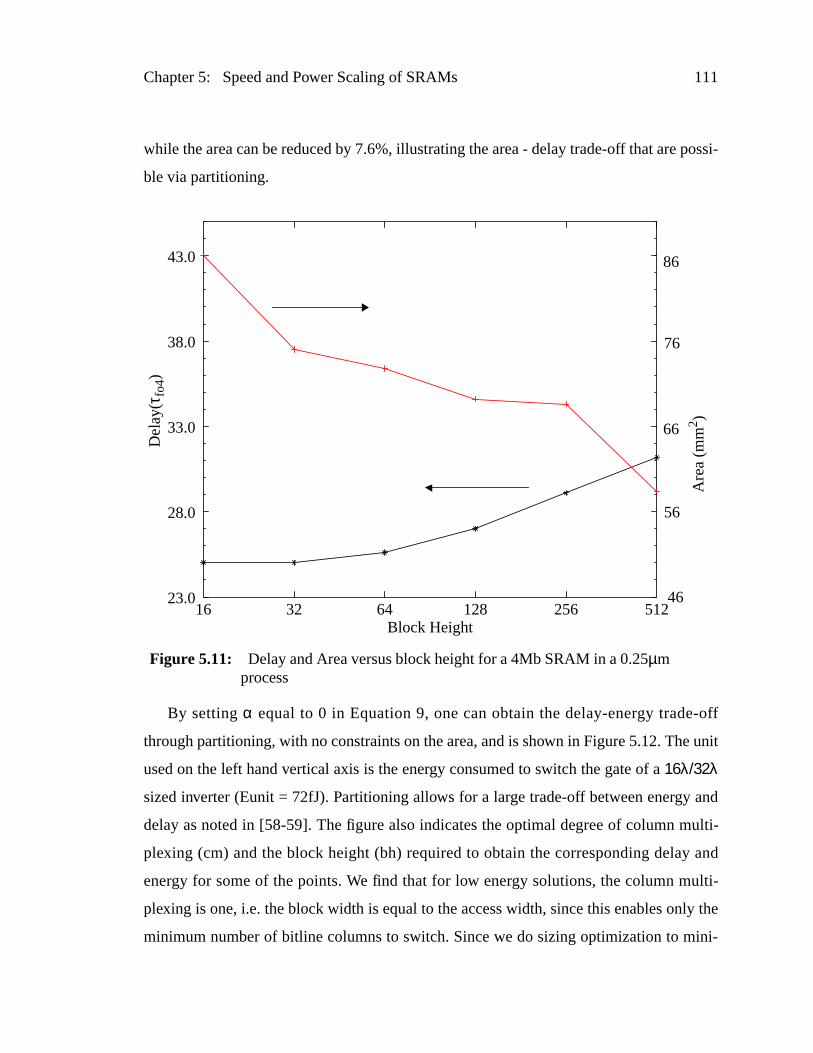
Chapter 5: Speed and Power Scaling of SRAMs 111
possi-
-off
unit
and
ulti-
and
ulti-
ly the
ini-
while the area can be reduced by 7.6%, illustrating the area - delay trade-off that are
ble via partitioning.
By settingα equal to 0 in Equation 9, one can obtain the delay-energy trade
through partitioning, with no constraints on the area, and is shown in Figure 5.12. The
used on the left hand vertical axis is the energy consumed to switch the gate of a16λ/32λ
sized inverter (Eunit = 72fJ). Partitioning allows for a large trade-off between energy
delay as noted in [58-59]. The figure also indicates the optimal degree of column m
plexing (cm) and the block height (bh) required to obtain the corresponding delay
energy for some of the points. We find that for low energy solutions, the column m
plexing is one, i.e. the block width is equal to the access width, since this enables on
minimum number of bitline columns to switch. Since we do sizing optimization to m
16 32 64 128 256 512Block Height
23.0
28.0
33.0
38.0
43.0
Del
ay(τ f
o4)
46
56
66
76
86
Are
a (m
m2 )
Figure 5.11: Delay and Area versus block height for a 4Mb SRAM in a 0.25µmprocess
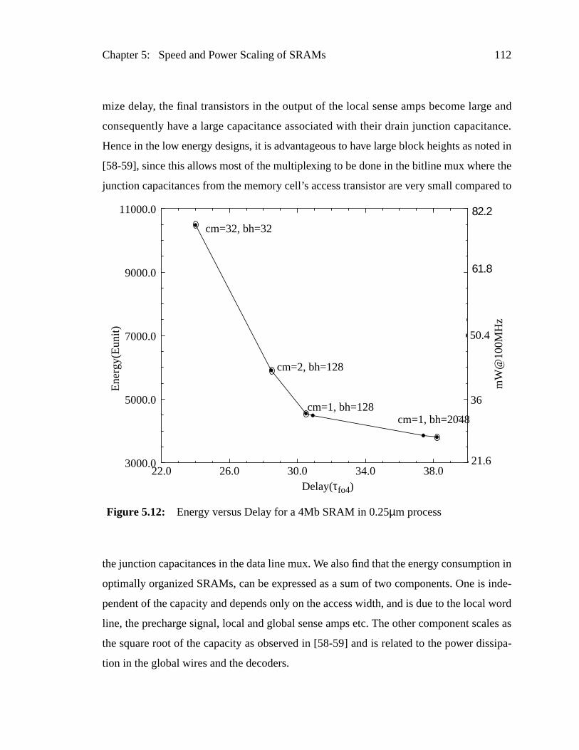
Chapter 5: Speed and Power Scaling of SRAMs 112
e and
tance.
ted in
the
red to
ion in
inde-
l word
ales as
ssipa-
mize delay, the final transistors in the output of the local sense amps become larg
consequently have a large capacitance associated with their drain junction capaci
Hence in the low energy designs, it is advantageous to have large block heights as no
[58-59], since this allows most of the multiplexing to be done in the bitline mux where
junction capacitances from the memory cell’s access transistor are very small compa
the junction capacitances in the data line mux. We also find that the energy consumpt
optimally organized SRAMs, can be expressed as a sum of two components. One is
pendent of the capacity and depends only on the access width, and is due to the loca
line, the precharge signal, local and global sense amps etc. The other component sc
the square root of the capacity as observed in [58-59] and is related to the power di
tion in the global wires and the decoders.
22.0 26.0 30.0 34.0 38.0Delay(τfo4)
3000.0
5000.0
7000.0
9000.0
11000.0
Ene
rgy(
Eun
it)
cm=32, bh=32
cm=2, bh=128
cm=1, bh=128cm=1, bh=2048
21.6
36
50.4
mW
@10
0MH
z
61.8
82.2
Figure 5.12: Energy versus Delay for a 4Mb SRAM in 0.25µm process
Chapter 5: Speed and Power Scaling of SRAMs 113
re to
uld
shown
d the
e-off
will be
sign
ct of
and
pro-
ue to
(wire
he
ngs in
of an
the
an be
using
ion.
one to
The trade-off curves of Figures 5.10 and 5.12 can be improved upon if one we
also perform transistor size optimization along with partition optimization. We wo
expect the optimal trade-off curves to have the same high speed end point as those
in the figures, but rotated towards the origin (since the sizing is done for fastest spee
corresponding end point is already optimal). We would also expect the optimal trad
curve to support smaller block sizes since the area and energy overhead of these
offset by the smaller transistor sizes.
5.4 Conclusions
Analytical models for delay, area and energy, allows one to explore a range of de
possibilities in a very short span of time. These models are used to study the impa
SRAM partitioning and it is found that a substantial trade-off between area, delay
energy can be obtained via the choice of SRAM organization.
The models are also used to predict the scaling trends of delay with capacity and
cess technology. The delay of SRAM can be broken into two components, one is d
the transistors in the technology (gate delay) and the other is due to the interconnect
delay). The gate delay increases by about 1.2τfo4 for every doubling of the RAM size,
starting with 15τfo4 for a 64Kb RAM, when a static circuit style is used to design t
decoders.
Non-scaling of threshold mismatches with process scaling, causes the signal swi
the bitlines and data lines also not to scale, leading to an increase in the gate delay
SRAM across technology generations. For an optimally organized 4Mb SRAM,
increase in delay is about 2τfo4 in the 0.1µm and 3.6τfo4 in the 0.07µm generations, and
is worse for other organizations. This delay increase for most SRAM organizations c
mitigated by using more hierarchical designs for the bitline and data line paths, and
offset compensation techniques like in [60, 64].
The wire delay starts becoming important for RAMs beyond the 1Mb generat
Across process shrinks, the wire delay becomes worse and wire redesign has to be d
Chapter 5: Speed and Power Scaling of SRAMs 114
ture
er the
and
f light
f
AM
e [65]),
array.
keep the wire delay in the same proportion to the gate delay. Divided word line struc
for the decoders, and column muxing for the bitline path, opens up enough space ov
array for using fat wires, and these can be used to control the wire delay for 4Mb
smaller designs across process shrinks. The wire delay is lower bounded by speed o
and this is about 1.75τfo4 for the 4Mb SRAM, and doubles with every quadrupling o
capacity. Thus for high performance RAM designs at the 16Mb and higher level, the R
architecture needs to be changed to use routing of address and data (see for exampl
instead of the current approach where the signals are broadcast globally across the
Chapter
AM
niques
timal
sult
mini-
ition.
le-
s that
ld be
ance
fers.
do a
to the
effort
the
tions.
. The
sizing
i-
izing
s, as
tic of
6 Conclusions
In this thesis we looked at design trade offs for fast low power SRAMs. The SR
access path is split into two portions: the row decoders and the read data path. Tech
to optimize both of these were investigated. In Chapter 3 we sketched out the op
decoder structure for fast low power SRAMs. Optimal decoder implementations re
when the decoder, excluding the predecoder, is implemented as a binary tree. This
mizes the power dissipation as only the smallest number of long decode wires trans
Also this doesn’t introduce any delay penalty if the 2-input NAND function is imp
mented in the source coupled style, since in this style the delay is almost the same a
of an inverter. Except for the final word driver in the decoder, all the other stages shou
implemented using skewed circuit techniques with self resetting. The highest perform
predecoders will have a NOR style wide fanin input stage followed by skewed buf
When this is coupled with a technique like that presented by Nambu et.al. in [21] to
selective discharge of the output, the power dissipation is very reasonable compared
speed gains that can be achieved. With the NOR style predecoder the total path
becomes independent of the exact partitioning of the decode tree, which will allow
SRAM designer to choose the best memory organization, based on other considera
Transistor sizing offers a great tool to trade off delay and energy of the decoders
presence of RC limited interconnect within the decode structure makes the decoder
problem a little different from the sizing of only logic gates. Full blown numerical optim
zation techniques can be used to obtain the various design points. The simple s
heuristic of keeping a constant fanout of about 4 works well for high speed design
long as the wire delays are not significant. For fast lower power solutions, the heuris
115

Chapter 6: Conclusions 116
good
s in a
ings
sense
f their
low
lse
plica
ence
itions.
clock
with
This
d and
. The
ce as
t the
write
The
sense
This
nly for
heir
ed to
act of
reducing the sizes of the input stage in the higher levels of the decode tree allows for
trade-offs between delay and power. Getting the decode signal to the local word line
fast and low power manner solves half of the memory design problem.
The key to low power operation in the SRAM data path is to reduce the signal sw
in the high capacitance nodes like the bitlines and the data lines. Clocked voltage
amplifiers are essential for obtaining low sensing power, and accurate generation o
sense clock is required for high speed operation. An energy efficient way to obtain
voltage swings in the bitlines is to limit the word line pulse width, by controlling the pu
width of the block select signal. The pulse widths are regulated by the aid of a re
delay element which consists of a replica memory cell and a replica bitline and h
tracks the delay of the memory cell over a wide range of process and operating cond
Two variations of the technique were discussed and their use to generate the sense
was also demonstrated. We believe that this is a very simple and robust technique
very low area overhead and is easily applicable to a wide variety of SRAM designs.
method can also be used to design a low swing data line operation for both the rea
write accesses, by pulsing the control signal which gates the drivers of these lines
pulse width is controlled by discharging a replica line which has the same capacitan
the worst case data line. This replica line is also used to trigger the amplifiers a
receiving end of these lines. We finally presented a technique to achieve low bitline
power, by using small voltage swings on the bitlines during the write operation.
memory cell structure is modified such that the cells can be used as latch type
amplifier to amplify and store the small swing write data presented on the bitlines.
technique requires boosted word lines and 20% larger area and hence is suitable o
certain niche applications.
We finally looked at scaling trends of delay and power in SRAMs as a function of t
size and technology. Simple analytical models for delay, area and energy are us
explore a range of design possibilities. These models are used to study the imp
Chapter 6: Conclusions 117
and
pro-
ue to
(wire
he
ngs in
RAM
se in
r
ated
ense
ion.
one to
cture
er the
and
speed
-
vel,
ee for
obally
e cell
hus
SRAM partitioning and it is found that a substantial trade-off between area, delay
energy can be obtained via the choice of SRAM organization.
The models are also used to predict the scaling trends of delay with capacity and
cess technology. The delay of SRAM can be broken into two components, one is d
the transistors in the technology (gate delay) and the other is due to the interconnect
delay). The gate delay increases by about 1.2τfo4 for every doubling of the RAM size,
starting with 15τfo4 for a 64Kb RAM, when a static circuit style is used to design t
decoders.
Non-scaling of threshold mismatches with process scaling, causes the signal swi
the bitlines and data lines also not to scale, leading to an increase in the delay of an S
across technology generations. For an optimally organized 4Mb SRAM, the increa
delay is about 2τfo4 in the 0.1µm and 3.6τfo4 in the 0.07µm generations, and is worse fo
other organizations. This delay increase for most SRAM organizations can be mitig
by using more hierarchical designs for the bitline and data line paths, and using s
amplifier offset compensation techniques like in [60, 64].
The wire delay starts becoming important for RAMs beyond the 1Mb generat
Across process shrinks, the wire delay becomes worse and wire redesign has to be d
keep the wire delay in the same proportion to the gate delay. A divided word line stru
for the decoders, and column muxing for the bitline path, opens up enough space ov
array for using fat wires, and these can be used to control the wire delay for 4Mb
smaller designs across process shrinks. The wire delay has a lower bound set by the
of light and this is about 1.75τfo4 for the 4Mb SRAM, and doubles with every quadru
pling of capacity. Thus for high performance RAM designs at the 16Mb and higher le
the RAM architecture needs to be changed to use routing of address and data (s
example [65]), instead of the current approach where the signals are broadcast gl
across the array. Wire delay is also directly proportional to the cell area, and henc
designs with smaller area will win out for large RAMs, even if the cells are weaker. T

Chapter 6: Conclusions 118
l be
the DRAM cell, multi-valued cells, TFT based cells, and other novel cell designs wilworth investigating for designing future high performance high capacity RAMs.

Appendix A
Optimum sizing of buffer chainswith intermediate interconnect
ers
e and
In this appendix we will derive the conditions for optimum fan up of chains of buff
with intermediate interconnect. For a simple chain of inverters driving some fixed loadCL,
the optimum fan up,f, is obtained by solving (1). In this equationp is the ratio of drain
junction capacitance to the gate capacitance. We will first solve the two subchain cas
then use the results to solve the three subchain case.
f( )ln 1– pf---– 0= (1)
119
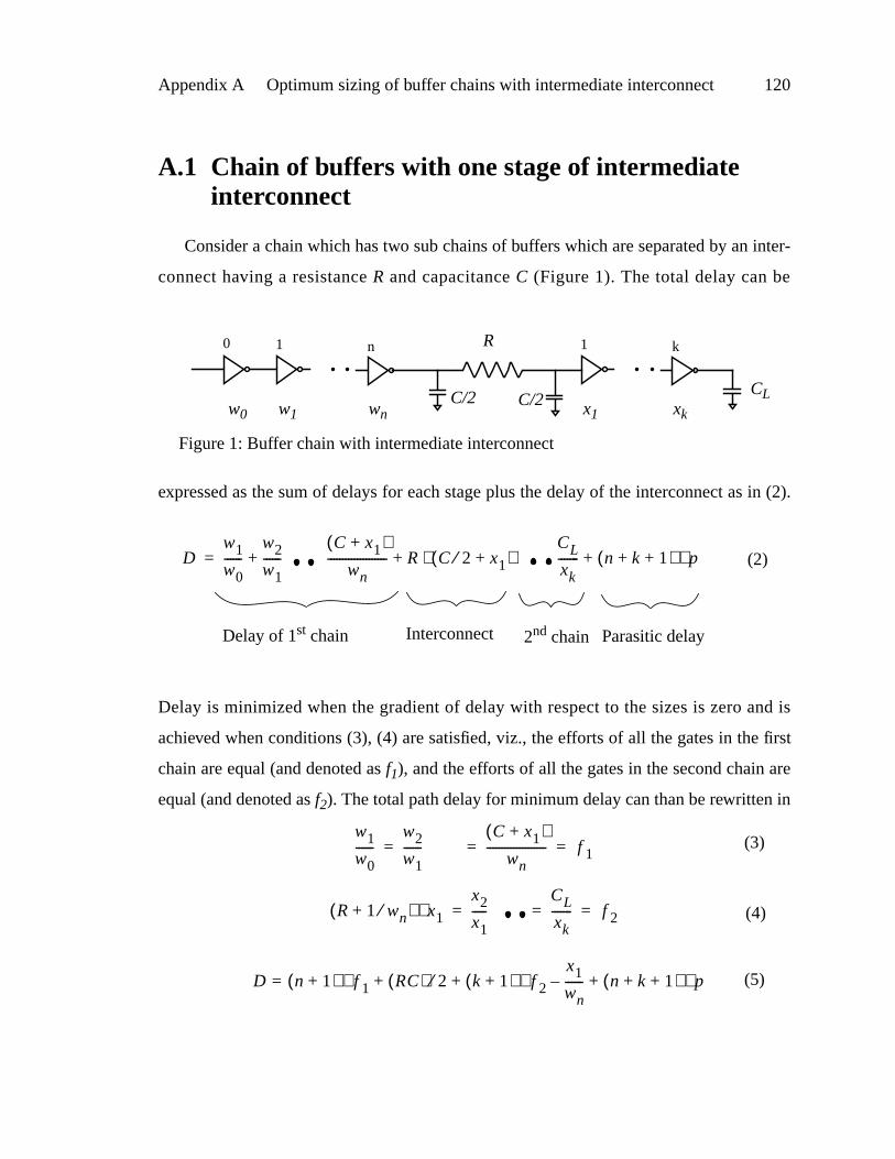
Appendix A Optimum sizing of buffer chains with intermediate interconnect 120
inter-
in (2).
nd is
first
are
in
A.1 Chain of buffers with one stage of intermediateinterconnect
Consider a chain which has two sub chains of buffers which are separated by an
connect having a resistanceR and capacitanceC (Figure 1). The total delay can be
expressed as the sum of delays for each stage plus the delay of the interconnect as
Delay is minimized when the gradient of delay with respect to the sizes is zero a
achieved when conditions (3), (4) are satisfied, viz., the efforts of all the gates in the
chain are equal (and denoted asf1), and the efforts of all the gates in the second chain
equal (and denoted asf2). The total path delay for minimum delay can than be rewritten
w0
0 1 n
w1 wn
CL
R
C/2C/2
1 k
x1 xk
Figure 1: Buffer chain with intermediate interconnect
Dw1
w0------
w2
w1------+=
C x1+( )wn
-------------------- R C 2⁄ x1+( )⋅+CL
xk------- n k 1+ +( ) p⋅+ (2)
Delay of 1st chain Interconnect 2nd chain Parasitic delay
w1
w0------
w2
w1------=
C x1+( )wn
--------------------= f 1=
R 1 wn⁄+( ) x1⋅x2
x1-----=
CL
xk-------= f 2=
(3)
(4)
D n 1+( ) f 1⋅ RC( ) 2⁄ k 1+( )+ f 2
x1
wn------–⋅+= n k 1+ +( ) p⋅+ (5)
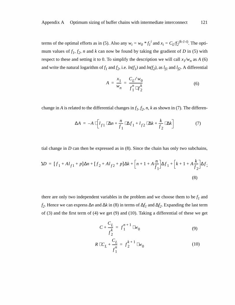
Appendix A Optimum sizing of buffer chains with intermediate interconnect 121
ains,
get
terms of the optimal efforts as in (5). Also anywi = w0 * f1i andxi = CL/f2
(k-1-i). The opti-
mum values off1, f2, n andk can now be found by taking the gradient ofD in (5) with
respect to these and setting it to 0. To simplify the description we will callx1/wn asA (6)
and write the natural logarithm off1 andf2, i.e. ln(f1) andln(f2), aslf1 andlf2. A differential
change inA is related to the differential changes inf1, f2, n, kas shown in (7). The differen-
tial change inD can then be expressed as in (8). Since the chain has only two subch
there are only two independent variables in the problem and we choose them to bef1 and
f2. Hence we can express∆n and∆k in (8) in terms of∆f1 and∆f2. Expanding the last term
of (3) and the first term of (4) we get (9) and (10). Taking a differential of these we
Ax1
wn------
CL w0⁄
f 1n
f 2k⋅
-----------------= = (6)
A∆ A– l f 1 n∆⋅ nf 1------ f 1∆⋅ l f 2 k∆⋅ k
f 2------ k∆⋅+ + +⋅= (7)
D∆ f 1 Al f 1 p+ +[ ] n∆ f 2 Al f 2 p+ +[ ] k∆ n 1 Anf 1------+ + f 1∆ k 1 A
kf 2------+ + f 2∆+ + +=
(8)
CCL
f 2k
-------+ f 1n 1+
w0⋅=
R CL⋅CL
f 1n
-------+ f 2k 1+
w0⋅=
(9)
(10)
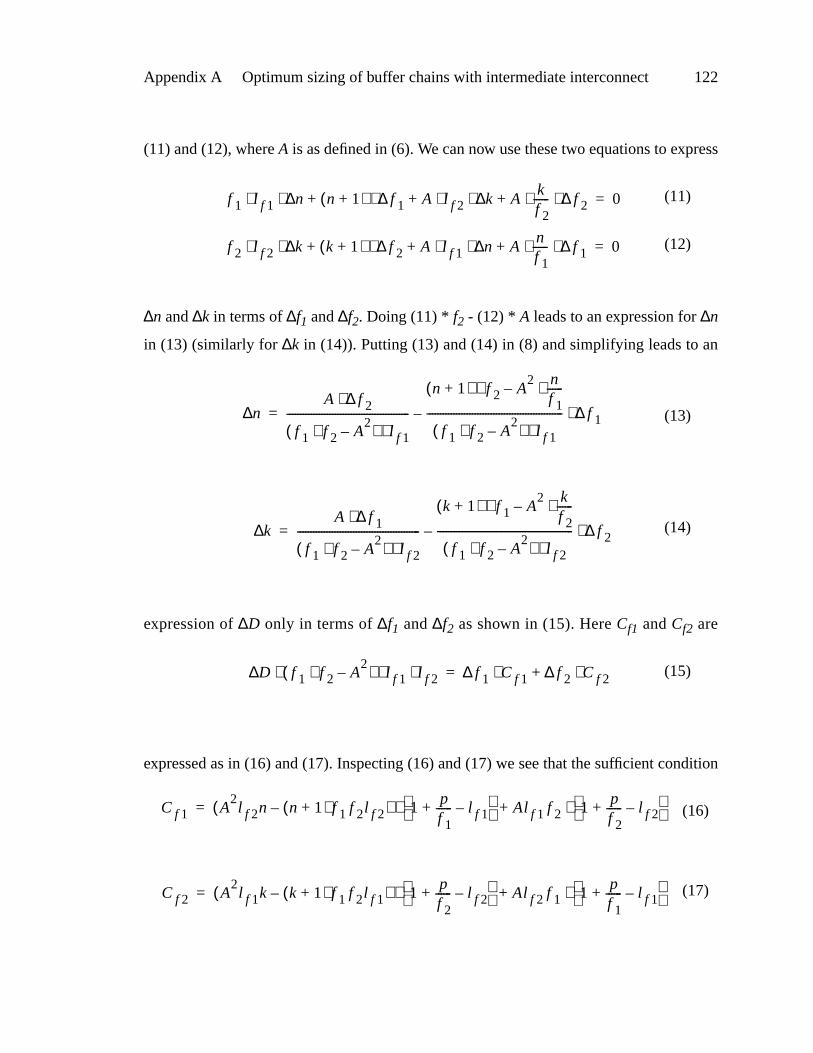
Appendix A Optimum sizing of buffer chains with intermediate interconnect 122
ress
n
dition
(11) and (12), whereA is as defined in (6). We can now use these two equations to exp
∆n and∆k in terms of∆f1 and∆f2. Doing (11) * f2 - (12) * A leads to an expression for∆n
in (13) (similarly for∆k in (14)). Putting (13) and (14) in (8) and simplifying leads to a
expression of∆D only in terms of∆f1 and∆f2 as shown in (15). HereCf1 andCf2 are
expressed as in (16) and (17). Inspecting (16) and (17) we see that the sufficient con
f 1 l f 1 n∆⋅ ⋅ n 1+( ) f 1∆⋅ A l f 2 k∆⋅ ⋅ Akf 2------ f 2∆⋅ ⋅+ + + 0=
f 2 l f 2 k∆⋅ ⋅ k 1+( ) f 2∆⋅ A l f 1 n∆⋅ ⋅ Anf 1------ f 1∆⋅ ⋅+ + + 0=
(11)
(12)
n∆A f 2∆⋅
f 1 f 2 A2
–⋅( ) l f 1⋅----------------------------------------------
n 1+( ) f 2⋅ A2 n
f 1------⋅–
f 1 f 2⋅ A2
–( ) l f 1⋅--------------------------------------------------- f 1∆⋅–= (13)
k∆A f 1∆⋅
f 1 f 2 A2
–⋅( ) l f 2⋅----------------------------------------------
k 1+( ) f 1⋅ A2 k
f 2------⋅–
f 1 f 2⋅ A2
–( ) l f 2⋅--------------------------------------------------- f 2∆⋅–= (14)
D∆ f 1 f 2⋅ A2
–( ) l f 1 l f 2⋅ ⋅ ⋅ f 1∆ Cf 1⋅ f 2∆ Cf 2⋅+= (15)
Cf 1 A2l f 2n n 1+( ) f 1 f 2l f 2–( ) 1 p
f 1------ l f 1–+
⋅ Al f 1 f 2 1 pf 2------ l f 2–+
⋅+= (16)
C f 2 A2l f 1k k 1+( ) f 1 f 2l f 1–( ) 1 p
f 2------ l f 2–+
⋅ Al f 2 f 1 1 pf 1------ l f 1–+
⋅+= (17)
Appendix A Optimum sizing of buffer chains with intermediate interconnect 123
lution
r
the
load.
river
asit-
lay of
for ∆D to be zero is that (18) and (19) be satisfied and both of these have the same so
as (1) for the single buffer case.
Thusf1 = f2 = f (which is about 4). Substituting this in (9) and (10) we can solve fon
andk and are given in (20) and (21). Multiplying these two equations and rearranging
terms we get (22) which relates the total number of stages in the chain to the output
Notice that this equation is very similar to the single chain case except that the input d
sizew0 is now derated by some factor which is only a function of the interconnect par
ics. Again rearranging the terms in (22) we get an expression forA which is dependent
only on the intermediate interconnect parasitics as shown in (23). Hence the total de
1 pf 1------ l f 1–+ 0=
1 pf 2------ l f 2–+ 0=
(18)
(19)
fn C
2 f w0------------- 1 1 4 f
RC--------++⋅=
fk RCL
2 f----------- 1 1 4 f
RC--------++⋅=
(20)
(21)
fn k 1+ + CL
w0
RC4 f-------- 1 1 4 f
RC--------++
2⋅
----------------------------------------------------
----------------------------------------------------= (22)
Ax1
wn------
CL w0⁄
fn k+
----------------- 4 f2RC
1 1 4 fRC--------++
2---------------------------------------= = = (23)
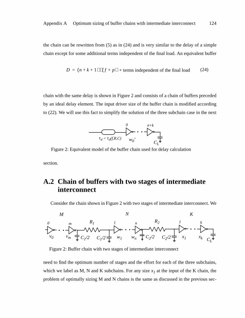
Appendix A Optimum sizing of buffer chains with intermediate interconnect 124
ple
uffer
eded
ding
next
t. We
hains,
sec-
the chain can be rewritten from (5) as in (24) and is very similar to the delay of a sim
chain except for some additional terms independent of the final load. An equivalent b
chain with the same delay is shown in Figure 2 and consists of a chain of buffers prec
by an ideal delay element. The input driver size of the buffer chain is modified accor
to (22). We will use this fact to simplify the solution of the three subchain case in the
section.
A.2 Chain of buffers with two stages of intermediateinterconnect
Consider the chain shown in Figure 2 with two stages of intermediate interconnec
need to find the optimum number of stages and the effort for each of the three subc
which we label as M, N and K subchains. For any sizex1 at the input of the K chain, the
problem of optimally sizing M and N chains is the same as discussed in the previous
D n k 1+ +( ) f p+( )⋅= + terms independent of the final load (24)
CL
0 n+k
w0’τd = τd(f,R,C)
Figure 2: Equivalent model of the buffer chain used for delay calculation
CL
R2
C2/2C2/2
1 k
x1 xk
Figure 2: Buffer chain with two stages of intermediate interconnect
R1
C1/2C1/2
1 n
w1 wn
0 m
v0 vm
M N K

Appendix A Optimum sizing of buffer chains with intermediate interconnect 125
delay
ed by
in is
s
the
tion and the optimum design has a stage effort of f and the number of stages and
given by (21), (22) and (24) respectively. Hence the M and N subchains can be replac
a single chain with no intermediate interconnect, but with an altered input driverv0’ as
shown in Figure 4. From the previous section, the optimum stage effort for the K cha
alsof. Hence even for the three subchain case, the optimum stage efforts isf for all the
stages. From (21) and Figure 4, we can write the expression fork as in (25). This can be
used to calculate the size ofx1 asCL/fk to give the loading for the first two subchains a
C2+x1. Again using (20) and (21) for the M and N chains with this output load yields
expressions form andn as in (26) and (27).
0 m+n
v0’CL
R2
C2/2C2/2
1 k
x1 xk
Figure 4: Equivalent model for delay calculation purposes
τd = τd(f, R1,C1)
fk R2CL
2 f-------------- 1 1 4 f
R2C2-------------++⋅= (25)
fn C2
C1------
1 1 4 fR2C2-------------++
4 fR1C1------------- 1+ 1–
------------------------------------------⋅=
fm C1 v0⁄
2 f---------------- 1 1 4 f
R1C1-------------++
⋅=
(26)
(27)

Appendix A Optimum sizing of buffer chains with intermediate interconnect 126
Appendix B
Delay and Energy Trade-off inRow Decoders
d by
). In
ber,
ts of
for a
via
r the
The delay energy trade-off curve with respect to transistor widths can be obtaine
minimizing the weighted objective function of the delay and energy as shown in (1
this Equation,λ is a lagrangian parameter which is a positive real number. Whenλ is 0,
the optimization leads to the fastest delay solution and when it is a large positive num
the optimization leads to the lowest energy solution and these form the two end poin
the delay energy curve. Intermediate points on this curve are obtained by optimizing
range of values forλ. Any point on this curve represents the fastest delay achievable
transistor sizing for the corresponding energy and equivalently, the lowest energy fo
minw1…wnD w1…wn( ) λ E w1…wn( )⋅+ (1)
127
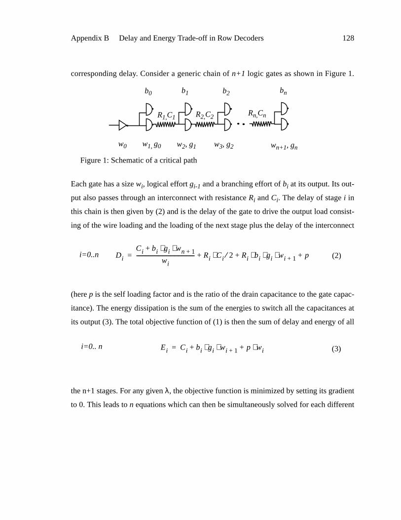
Appendix B Delay and Energy Trade-off in Row Decoders 128
.
sist-
nect
pac-
ces at
f all
nt
rent
corresponding delay. Consider a generic chain ofn+1 logic gates as shown in Figure 1
Each gate has a sizewi, logical effortgi-1 and a branching effort ofbi at its output. Its out-
put also passes through an interconnect with resistanceRi andCi. The delay of stagei in
this chain is then given by (2) and is the delay of the gate to drive the output load con
ing of the wire loading and the loading of the next stage plus the delay of the intercon
(herep is the self loading factor and is the ratio of the drain capacitance to the gate ca
itance). The energy dissipation is the sum of the energies to switch all the capacitan
its output (3). The total objective function of (1) is then the sum of delay and energy o
the n+1 stages. For any givenλ, the objective function is minimized by setting its gradie
to 0. This leads ton equations which can then be simultaneously solved for each diffe
w0 w1, g0 w2, g1
R1,C1
w3, g2 wn+1, gn
R2,C2 Rn,Cn
b0 b1 b2 bn
Figure 1: Schematic of a critical path
Di
Ci bi gi wn 1+⋅ ⋅+
wi-------------------------------------------- Ri Ci 2⁄⋅ Ri bi gi wi 1+⋅ ⋅ ⋅ p+ + += (2)i=0..n
Ei Ci bi gi wi 1+⋅ ⋅ p wi⋅+ += (3)i=0.. n

Appendix B Delay and Energy Trade-off in Row Decoders 129
qua-
ction
s is
qua-
ined.
an 1%
l path
λ to obtain then sizes, and a typical equation is shown in (4). The solution to these e
tions is guaranteed to be the minima due to the posynomial nature of the objective fun
[66]. We choose to solve then simultaneous equations using a iterative procedure. Thi
done by starting off with an initial guess for the sizes and then by repeatedly using e
tion (5) which is a reorganization of (4), a sequence of estimates for the sizes is obta
The procedure is terminated when a new estimate in this sequence differs by less th
from the previous one. The sizes are then used in a HSPICE simulation of the critica
to obtain the final delay and energy value for the point.
bi 1– gi 1–⋅wi 1–
---------------------------- Ri 1– bi 1– gi 1–⋅ ⋅ λ bi 1– gi 1– p+⋅( )⋅Ci bi gi wi 1+⋅ ⋅+
wi2
-------------------------------------------–+ + 0=
(4)
for i = 1.. n,
wi new,Ci bi gi wi 1+⋅ ⋅+
Ri 1– bi 1– gi 1–⋅ ⋅bi 1– gi 1–⋅
wi 1–---------------------------- λ bi 1– gi 1–⋅ p+( )⋅+ +
-------------------------------------------------------------------------------------------------------------------------------------------= (5)

Appendix B Delay and Energy Trade-off in Row Decoders 130

Appendix C
Technology Assumptions
lop-
used
dustry
ss
.
In this appendix we will describe all the assumptions that we have made for deve
ing the analytical models of Chapter 5. The technology described here is also the one
in Chapter 3 to compare various decoder architectures and is based on an actual in
process.
Technology
The base technology is assumed to be a 0.25µm CMOS process and the relevant proce
details are shown in Table C.1.
Parameter Value Comments
Cg 1.29 fF/µm Unit gate capacitance of an inverter (p-width = 2 xn-width)
Cj 1.72 fF/µm Unit parasitic junction capacitance of an inverter
Rg 4.4 KΩ/µm Unit output Resistance of an inverter
τfo4 [email protected] Delay of an inverter driving a load four times its size
M1 width 0.45µm Minimum width of metal 1
M1 aspectratio
1.5 Aspect ratio (height/width) of metal 1 cross section.
Table C.1: Features of the base 0.25µm technology
131
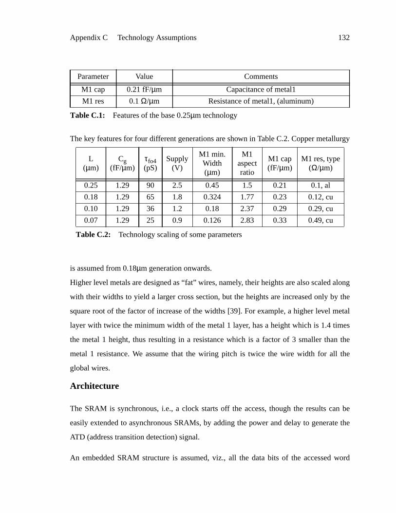
Appendix C Technology Assumptions 132
lurgy
along
y the
etal
es
n the
the
an be
te the
word
The key features for four different generations are shown in Table C.2. Copper metal
is assumed from 0.18µm generation onwards.
Higher level metals are designed as “fat” wires, namely, their heights are also scaled
with their widths to yield a larger cross section, but the heights are increased only b
square root of the factor of increase of the widths [39]. For example, a higher level m
layer with twice the minimum width of the metal 1 layer, has a height which is 1.4 tim
the metal 1 height, thus resulting in a resistance which is a factor of 3 smaller tha
metal 1 resistance. We assume that the wiring pitch is twice the wire width for all
global wires.
Architecture
The SRAM is synchronous, i.e., a clock starts off the access, though the results c
easily extended to asynchronous SRAMs, by adding the power and delay to genera
ATD (address transition detection) signal.
An embedded SRAM structure is assumed, viz., all the data bits of the accessed
M1 cap 0.21 fF/µm Capacitance of metal1
M1 res 0.1Ω/µm Resistance of metal1, (aluminum)
L(µm)
Cg(fF/µm)
τfo4(pS)
Supply(V)
M1 min.Width(µm)
M1aspectratio
M1 cap(fF/µm)
M1 res, type(Ω/µm)
0.25 1.29 90 2.5 0.45 1.5 0.21 0.1, al
0.18 1.29 65 1.8 0.324 1.77 0.23 0.12, cu
0.10 1.29 36 1.2 0.18 2.37 0.29 0.29, cu
0.07 1.29 25 0.9 0.126 2.83 0.33 0.49, cu
Table C.2: Technology scaling of some parameters
Parameter Value Comments
Table C.1: Features of the base 0.25µm technology

Appendix C Technology Assumptions 133
in
pad
of the
s.
hich
s are
duce
esults
lifier
l be of
mV,
e
M
ally
ense
[27]
5
come out of the memory core in close physical proximity to each other, unlike
stand-alone SRAMs, where the data I/O port locations are optimized for external
connections. Since this optimization adds a constant offset to the delay and power
SRAM core, the conclusions of this study are applicable even to stand-alone SRAM
The RAM cell size used for the analysis is 19.2λ x 32.8λ as in [21], and the cell area is
typical of high density six transistor CMOS layouts.
Circuit Style
The RAM is designed for high speed operation, with low power pulsed techniques w
reduce energy loss without affecting speed as discussed in [27]. The local wordline
pulsed to control the bitline swings and small swings are used in the datalines to re
power. Since these techniques do not affect the speed of the RAM, our analysis r
pertaining to delay scaling is applicable to any speed optimized SRAM design.
A latch style sense amplifier, with perfect timing control is assumed for the sense amp
as this consumes the least power and is the fastest. Hence our analysis results wil
relevance to both high speed and low power SRAMs. For the 0.25µm process, the optimal
input swing which minimizes the senseamp delay is found from simulations to be 100
of which 50mV is the input offset.
The transistors in the bitline mux have a fixed size of 16λ and those in the dataline mux ar
sized to be 50λ wide, to simplify the analysis. Circuit simulations indicate that the RA
delay is only weakly sensitive to the sizes of these transistors.
Energy Modeling
The swings in the bitlines and I/O lines are limited for low power operation. While ide
they should be limited to be exactly that required for optimum detection by the s
amps, in practical designs, there is some slack in how tightly they can be controlled
and hence are assumed to be twice the optimum signal swing. Thus for the 0.2µm
Appendix C Technology Assumptions 134
about
process, these swing by about 200mV since the optimal swing for the senseamps is100mV.
Bibliography
[1] P. Barnes, “A 500MHz 64b RISC CPU with 1.5Mb On-Chip Cache”,1999 IEEEInternational Solid State Circuits Conference, Digest of Technical Papers,pp.86-87.
[2] S. Hesley, et. al., “A 7th-Generation x86 Microprocessor”,1999 IEEEInternational Solid State Circuits Conference, Digest of Technical Papers, pp.92-93.
[3] Special issue on low power electronics.Proceedings of the IEEE, vol. 83, no. 4,April 1995.
[4] S. Subbanna, et. al., “A High-Density 6.9 sq.µm embedded SRAM cell in aHigh-Performance 0.25µm-generation CMOS Logic Technology”, IEDMTechnical Digest, pp. 275-278, 1996.
[5] G.G. Shahidi, et. al., “Partially-depleted SOI technology for digital logic”,ISSCCDigest of Technical Papers, Feb. 1999, pp. 426-427.
[6] A.P. Chandrakasan, et. al., “Low-Power CMOS Digital Design”,IEEE Journal ofSolid State Circuits, vol. 27, no. 4, p. 473-484, April 1992.
[7] W. Lee, et. al., “A 1V DSP for Wireless Communications”,1997 IEEEInternational Solid State Circuits Conference, Digest of Technical Papers, pp.92-93.
135
Bibliography 136
eof
gee
er
ed”,
ted,
lay,
OS
,ical
”,8.
[8] M. Izumikawa, et. al., “A 0.25-µm CMOS 0.9-V 100-MHz DSP Core”,IEEEJournal of Solid State Circuits, vol. 32, no. 1, pp. 52-61, Jan. 1997.
[9] K. Ishibashi, et. al., “A 1V TFT-Load SRAM using a Two-Step Word VoltagMethod”, 1992 IEEE International Solid State Circuits Conference, DigestTechnical Papers, pp. 206-207.
[10] H. Yamauchi, et. al., “A 0.5V / 100MHz Over-Vcc Grounded Data Stora(OVGS) SRAM Cell Architecture with Boosted Bit-Line and Offset SourcOver-Driving Schemes”,1996 IEEE International Symposium on Low PowElectronics and Design, Digest of Technical Papers, pp. 49-54.
[11] K. Itoh, A.R.Fridi, A. Bellaouar and M.I. Elmasry, “A deep sub-V, singlpower-supply SRAM cell with multi-Vt, boosted storage node and dynamic loa1996 Symposium on VLSI Circuits, Digest of Technical Papers, pp. 132-133.
[12] R. C. Jaeger, “Comments on ‘An optimized output stage for MOS integracircuits’,” IEEE Journal of Solid State Circuits, vol. SC-10, no. 3, pp. 185-186June 1975.
[13] C. Mead and L. Conway,Introduction to VLSI Systems,Reading, MA,Addison-Wesley, 1980.
[14] N. C. Li, et. al., “CMOS tapered buffer”,IEEE Journal of Solid State Circuits, vol.25, no. 4, pp. 1005-1008, August 1990.
[15] J. Choi, et. al., “Design of CMOS tapered buffer for minimum power-deproduct”, IEEE Journal of Solid State Circuits, vol. 29, no. 9, pp. 1142-1145September 1994.
[16] B. S. Cherkauer and E. G. Friedman, “A unified design methodology for CMtapered buffers”,IEEE Journal of Solid State Circuits, vol. 3, no. 1, pp. 99-110,March 1995.
[17] M. Yoshimoto, et. al., “A 64kb CMOS RAM with divided word line structure”I983 IEEE International Solid State Circuits Conference, Digest of TechnPapers, pp. 58-59.
[18] O. Minato, et. al., “2Kx8 bit Hi-CMOS static RAMs”,IEEE Journal of Solid StateCircuits, vol. SC-15, no. 4, pp. 656-660, August 1980.
[19] Y. Kohno, et. al., “A 14-ns 1-Mbit CMOS SRAM with variable bit organizationIEEE Journal of Solid State Circuits, vol. 29, no. 9, pp. 1060-1065, October 198
Bibliography 137
ith
of
ith
se,
e,
ideical
rol
e,
cal
[20] T. Chappell, et. al., “A 2-ns Cycle, 3.8-ns Access 512-Kb CMOS ECL SRAM wa Fully Pipelined Architecture”,IEEE Journal of Solid State Circuits,vol. 26, no.11, pp. 1577-1585, Nov. 1991.
[21] H. Nambu, et. al., “A 1.8ns Access, 550MHz 4.5Mb CMOS SRAM”,1998 IEEEInternational Solid State Circuits Conference, Digest of Technical Papers,pp.360-361.
[22] G. Braceras, et. al., “A 350MHz 3.3V 4Mb SRAM fabricated in a 0.3µm CMOSprocess”, 1997 IEEE International Solid State Circuits Conference, DigestTechnical Papers, pp. 404-405.
[23] K. Nakamura, et. al., “A 500MHz 4Mb CMOS pipeline-burst cache SRAM wpoint-to-point noise reduction coding I/O”, 1997 IEEE International Solid StateCircuits Conference, Digest of Technical Papers, pp. 406-407.
[24] K. Sasaki, et. al., “A 15-ns 1-Mbit CMOS SRAM”,IEEE Journal of Solid StateCircuits, vol. 23, no. 5, pp. 1067-1071, October 1988.
[25] K. Sasaki, et. al., “A 7-ns 140-mW 1-Mb CMOS SRAM with current senamplifier”, IEEE Journal of Solid State Circuits,vol. 27, no. 11, pp. 1511-1517November 1992.
[26] M. Matsumiya, et. al., “A 15-ns 16-Mb CMOS SRAM with interdigitated bit-linarchitecture”,IEEE Journal of Solid State Circuits,vol. 27, no. 11, pp. 1497-1502November 1992.
[27] B. Amrutur and M. Horowitz, “Techniques to Reduce Power in Fast WMemories”,1994 IEEE Symposium on Low Power Electronics, Digest of TechnPapers, p. 92-93.
[28] B. Amrutur and M. Horowitz, “A replica technique for word line and sense contin low-power SRAMs”,IEEE Journal of Solid State Circuits,vol. 33, no. 8, pp.1208-1219, August1998. pp. 1208-1219.
[29] K.W. Mai, et al. “Low-power SRAM design using half-swing pulse-modtechniques”,IEEE Journal of Solid State Circuits,vol. 33, no. 11, pp. 1659-1671November 1998.
[30] T. Mori, et. al., ““A 1 V 0.9 mW at 100 MHz 2 k*16 b SRAM utilizing ahalf-swing pulsed-decoder and write-bus architecture in 0.25µm dual-Vt CMOS”,1998 IEEE International Solid State Circuits Conference, Digest of TechniPapers, pp. 354-355.
Bibliography 138
iner
Md
heof
ack
its
ine,
ular
ory
[31] O. Minato, et. al., “A 20ns 64K CMOS SRAM”,1984 IEEE International SolidState Circuits Conference, Digest of Technical Papers, pp. 222-223.
[32] S. Yamamoto, et. al., “256k CMOS SRAM With Variable Impedance Data-LLoads”, IEEE Journal of Solid State Circuits,vol. SC-20, pp. 924-928, Octobe1985.
[33] K. J. Schultz, et. al., “Low-Supply-Noise Low-Power Embedded Modular SRAfor Mixed Analog-Digital ICs”, Proceedings of 1992 IEEE Custom IntegrateCircuits Conference, p. 7.1/1-4.
[34] P. Reed, et. al., “A 250MHz 5W RISC Microprocessor with On-Chip L2 CacController”, 1997 IEEE International Solid State Circuits Conference, DigestTechnical Papers, pp. 412-413.
[35] I. E. Sutherland and R. F. Sproull, “Logical effort: Designing for speed on the bof an envelope”, Advanced research in VLSI, pp. 1-16, 1991.
[36] Veendrick, H.J.M. et al. “Short-circuit dissipation of static CMOS circuitry andimpact on the design of buffer circuits”,IEEE Journal of Solid State Circuits,vol.SC-19, no. 4, pp. 468-473, August 1984.
[37] S. R. Vemuru and A. R. Thorbjornsen, “Variable-taper CMOS buffer”,IEEEJournal of Solid State Circuits, vol. 26, no. 9, pp. 1265-1269, September 1991.
[38] S. Ohbayashi, et. al., “A study of fanout optimization of SRAM decoder with a lcapacitance”,The Transactions of the IEICE, vol. E 73, no. 11, pp. 1855-1857November 1990.
[39] H. B. Bakoglu and J. D. Meindl, “Optimal interconnects for VLSI”,IEEETransactions on Electronic Devices, vol. ED-32, no. 5, pp. 903-909, May 1985.
[40] W. C. Elmore, “The transient response of damped linear networks with particregard to wide-band amplifiers”,Journal of Applied Physics,vol. 19, no. 1, pp.55-63, January 1948.
[41] HSPICE, Meta-Software, Inc., February 1996.
[42] H. C. Park, et. al., “A 833Mb/s 2.5V 4Mb double data rate SRAM”, 1998EEEInternational Solid State Circuits Conference, Digest of Technical Papers,pp.356-357.
[43] R. Heald and J. Holst, “A 6-ns cycle 256kb cache memory and memmanagement unit”,IEEE Journal of Solid State Circuits,vol. 28, pp. 1078-1083,November 1993.
Bibliography 139
”,
gof
ith
ble
for
[44] S. Murukami, et. al., “A 21-mW 4-Mb CMOS SRAM for Battery OperationIEEE Journal of Solid State Circuits, vol. 26, no. 11, pp. 1563-1569, Nov. 1991.
[45] T. Hirose, et. al., “A 20nS 4Mb CMOS SRAM with Hierarchical Word DecodinArchitecture”, 1990 IEEE International Solid State Circuits Conference, DigestTechnical Papers, pp.132-133.
[46] S. Flannagan, et. al., “8ns CMOS 64kx4 and 256kx1 SRAMs”,1990 IEEEInternational Solid State Circuits Conference, Digest of Technical Papers,pp.134-135.
[47] J.S. Caravella, “A Low Voltage SRAM For Embedded Applications”,IEEEJournal of Solid State Circuits, vol. 32, no. 3, pp. 428-432, March 1997.
[48] A.R. Pelella, et. al., “A 2ns Access, 500MHz 288Kb SRAM MACRO”,1996Symposium of VLSI Circuits, Digest of Technical Papers, pp.128-129.
[49] S. Tachibana, et. al., “A 2.6-ns Wave-Pipelined CMOS SRAM wDual-Sensing-Latch Circuits”,IEEE Journal of Solid State Circuits,vol. 30, no. 4,pp. 487-490, April 1995.
[50] S. E. Schuster, et. al., “A 15-ns CMOS 64K RAM”,IEEE Journal of Solid StateCircuits, vol. sc-21, no. 5, p. 704-711, October 1986.
[51] M. Shoji, “Elimination of Process-Dependent Clock Skew in CMOS VLSI”,IEEEJournal of Solid State Circuits, vol. sc-21, no. 5, p. 875-880, October 1986.
[52] J. L. Hennessy and D. A. Patterson,Computer Architecture a QuantitativeApproach, Morgan Kaufmann, 1996.
[53] A. L. Silburt, et. al., “A 180-MHz 0.8-µm BiCMOS Modular Memory Family ofDRAM and Multiport SRAM”, IEEE Journal of Solid State Circuits,vol. 28, no.3, p. 222-231, March 1993.
[54] K. Osada, et. al., “A 2ns Access, 285MHz, Two-Port Cache Macro using DouGlobal Bit-Line Pairs”,ISSCC Digest of Technical Papers, pp. 402-403, February1997.
[55] 1997 National Technology Roadmap for Semiconductor.
[56] T. Wada, S. Rajan and S. A. Przybylski, “An Analytical Access Time ModelOn-Chip Cache Memories”,IEEE Journal of Solid State Circuits, vol. 27, no. 8,pp. 1147-1156, August 1992.
Bibliography 140
l for
tion
ate
ent
ions.
toE
ply
e
”,
istor
OS
[57] S. J. E. Wilton and N. P. Jouppi, “An Enhanced Access and Cycle Time ModeOn-Chip Caches”,WRL Research Report 93/5, June 1994.
[58] R. J. Evans and P. D. Franzon, “Energy Consumption Modeling and Optimizafor SRAMs”, IEEE Journal of Solid State Circuits, vol. 30, no. 5, pp. 571-579,May 1995.
[59] R. J. Evans, “Energy consumption modeling and optimization for SRAMs”,Ph.D.dissertation, Dept. of Electrical and Computer Engineering, North Carolina StUniv., July 1993.
[60] K. Seno, et. al., “A 9-ns 16-Mb CMOS SRAM with offset-compensated currsense amplifier”,IEEE Journal of Solid State Circuits, vol.28, no. 11, Nov. 1993.
[61] J.D. Meindl et. al., “The impact of stochastic dopant and interconnect distributon gigascale integration”,1997 IEEE Int. Solid-State Circuits Conf., Dig. TechPapers, pp. 232-233.
[62] T. Mizuno, et. al., “Experimental Study of Threshold Voltage Fluctuation DueStatistical Variation of Channel Dopant Number in MOSFET’s”, IEETransactions of Electron Devices, Vol. 41, No. 11, p. 2216-2221, Nov. 1994.
[63] C. L. Portmann, et. al., “Metastability in CMOS library elements in reduced supand technology scaled applications”,IEEE Journal of Solid-State Circuits, vol.30,no.1, p. 39-46.
[64] K. Ishibashi, et. al., “A 6-ns 4-Mb CMOS SRAM with offset-voltage-insensitivcurrent sense amplifiers”,IEEE Journal of Solid State Circuits, vol. 30, no. 4,April 1995.
[65] T. Higuchi, et. al., “A 500MHz Synchronous Pipelined 1Mbit CMOS SRAMTechnical Report of IEICE,May 1996, pp. 9-14,(in Japanese).
[66] Fishburn, J.P. et al. “TILOS: a posynomial programming approach to transsizing” Held: Santa Clara, CA, USA 18-21 Nov. 1985.IEEE InternationalConference on Computer-Aided Design: ICCAD-85. Digest of Technical Papers
[67] Sakurai, T. et al. “Alpha-power law MOSFET model and its applications to CMinverter delay and other formulas”IEEE Journal of Solid State CircuitsApril1990. vol.25, no.2, pp. 584-94.