Design and Analysis of a Transversal Filter RFIC …daifa01/Top/PubPapers/2008/Jpaper...Design and...
7
Design and Analysis of a Transversal Filter RFIC in SiGe Technology Vasanth Kakani and Fa Foster Dai Auburn University &PROGRAMMABLE RF FILTERS have many applica- tions in communication systems. Their main purpose is to reconstruct a signal by implementing an inverse transfer function of the communication channels. In fiber communications, modal, chromatic, and polar- ization mode dispersions are the major sources of transmission impairments. 1 Some mechanical or optical solutions, such as dispersion-compensated fibers, have negative dispersion compared with common fibers. However, in long-haul systems, solutions incorporating dispersion-compensated fibers tend to be bulky and costly. They also have high insertion loss and slow tuning speed, if they are tunable at all. A solution in the electrical domain is equalization at the receiver end. Electronic transversal filters can compensate for fiber dispersions by being pro- grammed to construct an inverse transfer function of the dispersive channel and to restore the signal to its original form. 2–4 In the wireless domain, for multiband transceiver designs, programmable RF notch filters are needed to selectively reject the bands according to various wireless standards. RF notch filters are critical for removing unwanted signals such as images and interference. Moreover, low-cost, mass-produced elec- tronic filters—commonly used in tele- phone systems and disk drives—can be integrated on the same die with the receiver and can be implemented in either the digital or analog domain. Digital filters typically use shift registers or memory elements to implement the delay cell; the data must be sampled and digitized, which requires an A/D converter preceding the filter. Designing high-speed data converters is not trivial, because they greatly increase circuit complexity and power consumption. Analog imple- mentations, on the other hand, remove the need for power-hungry data converters before equalization, resulting in huge power savings. Researchers have explored the use of continuous-time filters based on G m -C transconductor-capacitor ladder and switched- capacitor filters for high-speed applications. They have also tackled intrinsic problems associated with analog implementations—for example, bias point offset, charge leakage, and parameter mismatch varia- tions—by innovative use of circuit, layout, and fabrication techniques. As signal speeds move into the gigahertz range, however, these analog techniques are ineffective, calling for RF or microwave solutions. Wu et al. describe a fractionally spaced transversal filter that uses passive transmission lines as delay elements. 5 However, passive delay elements occupy a large die area and provide accurate delays for only a narrow frequency band; moreover, they are not tunable on the fly. Our design is based on a commonly used SiGe (silicon-germanium) technology with transistor cutoff frequency e T 5 47 GHz, using broadband amplifiers to implement delay blocks. Thus, it can be integrated 0 IEEE Design & Test of Computers dtco-25-01-kaka.3d 14/12/07 12:52:10 0 Cust # kaka Editor’s note: Filters are a critical component of every high-speed data communications system. Die area, power consumption, and RFIC integration are primary concerns for filter designers. The authors of this article have designed and fabricated a low-power analog filter with greatly reduced die area compared to passive delay lines. This transversal filter design has been realized in 47- GHz SiGe process technology. —Craig Force, Texas Instruments Design and Test of RFIC Chips 0740-7475/08/$25.00 G 2008 IEEE Copublished by the IEEE CS and the IEEE CASS IEEE Design & Test of Computers
Transcript of Design and Analysis of a Transversal Filter RFIC …daifa01/Top/PubPapers/2008/Jpaper...Design and...

Design and Analysis of aTransversal Filter RFIC inSiGe TechnologyVasanth Kakani and Fa Foster Dai
Auburn University
&PROGRAMMABLE RF FILTERS have many applica-
tions in communication systems. Their main purpose
is to reconstruct a signal by implementing an inverse
transfer function of the communication channels. In
fiber communications, modal, chromatic, and polar-
ization mode dispersions are the major sources of
transmission impairments.1 Some mechanical or
optical solutions, such as dispersion-compensated
fibers, have negative dispersion compared with
common fibers. However, in long-haul systems,
solutions incorporating dispersion-compensated fibers
tend to be bulky and costly. They also have high
insertion loss and slow tuning speed, if they are
tunable at all.
A solution in the electrical domain is equalization
at the receiver end. Electronic transversal filters can
compensate for fiber dispersions by being pro-
grammed to construct an inverse transfer function of
the dispersive channel and to restore the signal to its
original form.2–4 In the wireless domain, for multiband
transceiver designs, programmable RF notch filters are
needed to selectively reject the bands according to
various wireless standards. RF notch filters are critical
for removing unwanted signals such as images and
interference. Moreover, low-cost, mass-produced elec-
tronic filters—commonly used in tele-
phone systems and disk drives—can be
integrated on the same die with the
receiver and can be implemented in
either the digital or analog domain.
Digital filters typically use shift registers
or memory elements to implement the
delay cell; the data must be sampled
and digitized, which requires an A/D
converter preceding the filter.
Designing high-speed data converters is
not trivial, because they greatly increase circuit
complexity and power consumption. Analog imple-
mentations, on the other hand, remove the need for
power-hungry data converters before equalization,
resulting in huge power savings. Researchers have
explored the use of continuous-time filters based on
Gm-C transconductor-capacitor ladder and switched-
capacitor filters for high-speed applications. They have
also tackled intrinsic problems associated with analog
implementations—for example, bias point offset,
charge leakage, and parameter mismatch varia-
tions—by innovative use of circuit, layout, and
fabrication techniques. As signal speeds move into
the gigahertz range, however, these analog techniques
are ineffective, calling for RF or microwave solutions.
Wu et al. describe a fractionally spaced transversal
filter that uses passive transmission lines as delay
elements.5 However, passive delay elements occupy a
large die area and provide accurate delays for only a
narrow frequency band; moreover, they are not
tunable on the fly.
Our design is based on a commonly used SiGe
(silicon-germanium) technology with transistor cutoff
frequency eT5 47 GHz, using broadband amplifiers to
implement delay blocks. Thus, it can be integrated
0IEEE Design & Test of Computers dtco-25-01-kaka.3d 14/12/07 12:52:10 0 Cust # kaka
Editor’s note:
Filters are a critical component of every high-speed data communications
system. Die area, power consumption, and RFIC integration are primary
concerns for filter designers. The authors of this article have designed and
fabricated a low-power analog filter with greatly reduced die area compared
to passive delay lines. This transversal filter design has been realized in 47-
GHz SiGe process technology.
—Craig Force, Texas Instruments
Design and Test of RFIC Chips
0740-7475/08/$25.00 G 2008 IEEE Copublished by the IEEE CS and the IEEE CASS IEEE Design & Test of Computers

into the entire receiver IC, thereby reducing cost. The
programmable RF filter’s measured forward voltage
gain (S21) parameter demonstrates various tuned-filter
characteristics such as low pass, high pass, band
reject, and notch with frequencies of up to 3.5 GHz.
Transversal filter designThe transversal filter is essentially a tapped delay
line with the feed-forward taps forming a finite impulse
response (FIR) filter. Figure 1 shows a block diagram
of a transversal filter. Each delay element delays the
input signal y(t) as it propagates through the filter. The
delayed version of the signal y(t – kT ), where k 5 1, 2,
3, … are the tap coefficients and T is the period by
which the signal is delayed, is tapped along the delay
line, and the outputs of these tap coefficients are
summed to generate the filter output. The integrated
filter’s transfer function can be adaptively adjusted by
changing the coefficients (c(0) … c(k)) of its tap
weights. Adjusting the tap weights lets us adapt 0s in
the overall transfer characteristics of the filter to
various frequencies and implement different filter
characteristics such as notch, band pass, low pass,
and band reject. Changing the tap weights affects only
the locations of the 0s; the poles of the programmable
filter are fixed, and hence the filter is always stable.
Delay stage
Passive delay networks are either lossy (RC delay
lines) or bulky (LC delay lines). Moreover, passive
delay networks are always narrowband; they are not
tunable on the fly, and they consume a large area on
the die. To overcome these drawbacks of passive
delay lines, we use active delay stages instead of
passive delay stages. A seven-tap equalizer would
require six delay amplifiers connected in series, so we
require the individual delay amplifiers to have
broadband characteristics with a high cutoff frequen-
cy. As individual amplifier cells are cascaded, the total
bandwidth at the output decreases according to the
following equation:
BWtot ~ BWc
ffiffiffiffiffiffiffiffiffiffiffiffiffiffi2
1n { 1
mp
ð1Þ
where BWc is the bandwidth of the individual
amplifier, BWtot is the total bandwidth of the
cascaded individual amplifiers, m is 2 for first-order
stages and 4 for second-order stages, and n is the
number of identical stages having bandwidth BWc.6
For a seven-tap equalizer with six delay stages, the
individual delay stages need a bandwidth of at least
10 GHz, for an overall bandwidth of 3.5 GHz.
Applying the principle of impedance mismatching
between succeeding stages—for example, creating
a chain of alternating transadmittance and transim-
pedance stages7—improves the bandwidth. We
chose the series-shunt cascaded Cherry-Hooper
amplifier to implement the filter delay stages.8 As
Figure 2 shows, the Cherry-Hooper amplifier is a
cascade of two feedback amplifiers: the series
feedback stage is a transconductance amplifier,
and the shunt feedback stage is a transimpedance
amplifier. Transistor Q1 and resistor RE (degenera-
tion resistance) form the serial feedback stage;
transistor Q3 and resistor RF (shunt feedback
resistance) form the shunt feedback stage. We
calculate the input and output resistances of the
serial feedback stage as
Rin ~ rb z rp z bRE ð2Þ
Rout ~ ro(1 z gmRE) ð3Þ
where rb is the base resistance, rp is the small-signal
base-emitter resistance, b is the small-signal-current
gain, ro is the output resistance, and gm is the small-
signal transconductance. We calculate the input and
output resistances of the shunt feedback stage as
Rin ~rb
bz
1
gm
� �1 z
RF
RL
� �ð4Þ
0IEEE Design & Test of Computers dtco-25-01-kaka.3d 14/12/07 12:52:12 1 Cust # kaka
Figure 1. In this block diagram of the transversal filter, delay
amplifiers are labeled T, denoting the period by which the
signal is delayed; variable-gain amplifiers are labeled fl, and
their gain can be tuned from 0 to 1.
January/February 2008

Rout ~1
gmz
RF z rb
bð5Þ
where RL is the load resistance. Equations 4 and 5
show that with these two stages cascaded, the high
resistive input of the series feedback stage is driven
from a low-resistance voltage output obtained from
the shunt feedback stage.
Conversely, the low resistive input of the shunt
feedback stage is driven by a high-resistance current
output obtained from the serial feedback stage. As a
result, all the signal nodes effectively have low
resistance values, yielding only high-frequency poles;
this improves the amplifier bandwidth because of the
low time constants associated at the signal nodes. This
arrangement is also advantageous because the imped-
ance requirement will be automatically satisfied at the
amplifier’s input and output when several such delay
stages are cascaded. Emitter followers between the
delay stages provide level shifting and create stronger
impedance mismatch between succeeding stages to
improve the bandwidth. Another advantage of this
impedance mismatch between succeeding stages is
that it causes all the nodes to have low resistance
values, thereby reducing the influence of parasitic
capacitance, which can affect the time constants
associated with those nodes.
In reality, the input and output impedances of the
amplifier stages are frequency dependent, and at high
frequencies the impedance mismatching can be
degraded and the bandwidth reduced. To overcome
these effects, we can use the additional elements
shown in Figure 2 (capacitors CF and CE) in the
feedback path to improve the bandwidth.
The degeneration and feedback capacitors, CE and
CF, introduce 0s in the frequency response and thereby
maximize the amplifier bandwidth. Emitter degenera-
tion RE and CE at the transconductance pair creates
the first 0. The pole caused by RF and CF in the
feedback path of the transimpedance pair creates the
second 0. These two 0s enhance the bandwidth and
eliminate the need for inductors. The transfer function
of the Cherry-Hooper amplifier, including the capac-
itors, can be approximated as
Vout
Vin
~gm1(1 z sCERE)(1 z sCFRF z gm3RF)
gm3(1 z sCFRF)(1 z sCERE z gm1RE)
ð6Þ
where Vout and Vin are the output and input
voltages, CE is the degeneration capacitance, CF is
the shunt feedback capacitance, and gm1 and gm3
are the transconductances of transistors Q1 and Q3
in Figure 2. The designed amplifier has a 3-dB cutoff
frequency of 10 GHz.
Tap gain stage
The function of the gain stage is to implement tap
weight coefficients to adaptively adjust the transversal
filter’s transfer function. The tap weights should be
continuously adjustable between 0 and 1 and should
also be able to provide a phase shift of 180 degrees to
give negative tap coefficients. As Figure 3 shows, the
transversal filter tap with programmable gain imple-
mentation uses the Gilbert variable-gain amplifier. The
use of the Gilbert cell to implement positive and
negative tap coefficients was first reported by Lee and
Freundorfer.9 Transistors Q3, Q4, Q5, and Q6 form the
core current-gain-control circuit. VAGC is the differen-
tial gain control input used to set the tap weights. For
sufficiently large values of VAGC, the current is steered
to the top differential pairs, and the gain from Iout to Vin
is at either its maximum or minimum value. When the
differential VAGC signal is 0, the gain is 0. Tap weights
0IEEE Design & Test of Computers dtco-25-01-kaka.3d 14/12/07 12:52:13 2 Cust # kaka
Figure 2. Cherry-Hooper amplifier used to implement
delay stages.
Design and Test of RFIC Chips
IEEE Design & Test of Computers
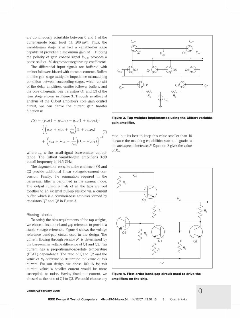
are continuously adjustable between 0 and 1 of the
current-mode logic level (6 200 mV). Thus, the
variable-gain stage is in fact a variable-loss stage
capable of providing a maximum gain of 1. Flipping
the polarity of gain control signal VAGC provides a
phase shift of 180 degrees for negative tap coefficients.
The differential input signals are buffered with
emitter followers biased with constant currents. Buffers
and the gain stage satisfy the impedance mismatching
condition between succeeding stages, which consist
of the delay amplifiers, emitter follower buffers, and
the core differential pair transistors Q1 and Q3 of the
gain stage shown in Figure 3. Through small-signal
analysis of the Gilbert amplifier’s core gain control
circuit, we can derive the current gain transfer
function as
I(s) ~ gm3(1 z scp4rb) { gm4(1 z scp3rb)f g:
gm3 z scp3 z1
rp3
� �(1 z scp4rb)
�
z gm4 z scp4 z1
rp4
� �(1 z scp3rb)
�{1
ð7Þ
where cp is the small-signal base-emitter capaci-
tance. The Gilbert variable-gain amplifier’s 3-dB
cutoff frequency is 14.5 GHz.
The degeneration resistors at the emitters of Q1 and
Q2 provide additional linear voltage-to-current con-
version. Finally, the summation required in the
transversal filter is performed in the current mode.
The output current signals of all the taps are tied
together to an external pull-up resistor via a current
buffer, which is a common-base amplifier formed by
transistors Q7 and Q8 in Figure 3.
Biasing blocks
To satisfy the bias requirements of the tap weights,
we chose a first-order band-gap reference to provide a
stable voltage reference. Figure 4 shows the voltage
reference band-gap circuit used in the design. The
current flowing through resistor R1 is determined by
the base-emitter voltage difference of Q1 and Q2. This
current has a proportional-to-absolute temperature
(PTAT ) dependence. The ratio of Q1 to Q2 and the
value of R1 combine to determine the value of this
current. For our design, we chose 100 mA for this
current value; a smaller current would be more
susceptible to noise. Having fixed the current, we
chose 6 as the ratio of Q1 to Q2. We could choose any
ratio, but it’s best to keep this value smaller than 10
because the matching capabilities start to degrade as
the area spread increases.10 Equation 8 gives the value
of R1.
0IEEE Design & Test of Computers dtco-25-01-kaka.3d 14/12/07 12:52:13 3 Cust # kaka
Figure 4. First-order band-gap circuit used to drive the
amplifiers on the chip.
Figure 3. Tap weights implemented using the Gilbert variable-
gain amplifier.
January/February 2008

R1 ~VT ln (c)
IPTATð8Þ
where c is the ratio of transistor Q1 to
transistor Q2, and VT is the thermal
voltage.
We chose the value of R2 so that the
current flowing through it has an equal
and opposite temperature coefficient
called IPTAT and could be calculated
from Equations 9 and 10:
d(IPTAT)
dT~ (1=R2)
d(Vbe)
dTð9Þ
d(IPTAT)
dT
~ (1=R2)
Vg0 {T
TrVgo { Vbe(Tr)� �� � ð10Þ
where Vg0 is the band-gap voltage at 0 Kelvin and
Vbe(Tr) is the base-emitter voltage at room temper-
ature.
Having chosen the values of R1 and R2, we find
in Figure 4 that the current flowing at the collector
of Q1 is the sum of the PTAT and IPTAT (inversely
proportional to absolute temperature) currents, and
we have a constant current at that node. The
voltage drop across the resistor connected to the
collector of Q1 (VQ1) is also temperature indepen-
dent. However, reference voltage Vref 5 VQ1(con-
stant) + Vbe3. Assuming that Vbe3 and the Vbe of the
current biasing transistors of bipolar current-mode
logic circuits match, Vref can be used to drive the
base of those current biasing transistors, to provide
a constant voltage swing independent of tempera-
ture.
If we delete R2 and Q3, then Vref has PTAT
characteristics, and when used to drive the base
of the current biasing transistors of bipolar
amplifiers, Vref would provide constant transcon-
ductance.
The tap weights feed into the equalizer through a
single-ended-to-differential converter. A differential
pair takes a single-ended input and steers the current
to one of the two transistors in the differential pair. The
product of the current and the load resistor is the
output logic level.
0IEEE Design & Test of Computers dtco-25-01-kaka.3d 14/12/07 12:52:14 4 Cust # kaka
Figure 5. Transversal filter chip die photo.
Figure 6. Measured filter-transfer function with notch at 2 GHz.
The seven tap coefficients of the filter are set as –85 mV,
30 mV, –20 mV, 0 mV, 30 mV, 0 mV, and 0 mV. The magnitude
of the notch is –43 dB, which provides a notch rejection of
–30 dB compared with the pass-band magnitude.
Design and Test of RFIC Chips
IEEE Design & Test of Computers
Prototype design and measurementsThe 3.5-GHz, seven tap transversal filter was
implemented in 45-GHz SiGe technology with a total
die area of 2.16 mm2, including pads. The chip
consumes 250 mW. The filter RFIC includes a band-
gap reference to provide temperature-independent
constant current sources for the amplifiers. The filter
RFIC also includes an input buffer, output buffers, and
single-ended-to-differential converters. Figure 5 is a die
photo of the transversal filter RFIC.
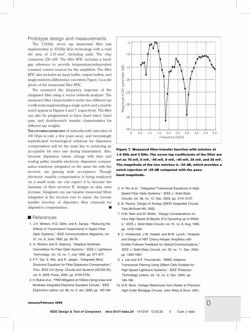
We measured the frequency response of the
integrated filter using a vector network analyzer. The
measured filter characteristics under two different tap
coefficients implementing a single notch and a double
notch appear in Figures 6 and 7, respectively. The filter
can also be programmed to have band reject, band
pass, and double-notch transfer characteristics for
different tap weights.
THE UPCOMING GENERATION of networks with data rates of
100 Gbps is only a few years away, and increasingly
sophisticated technological solutions for dispersion
compensation will be the main key to achieving an
acceptable bit error rate during transmission. Also,
because dispersion values change with time and
routing paths, tunable electronic dispersion compen-
sation solutions, integrated on the same die with the
receiver, are gaining wide acceptance. Though
electronic tunable compensation is being employed
on a small scale, we can expect it to become the
mainstay of fiber receiver IC designs as data rates
increase. Designers can use tunable transversal filters
integrated at the receiver end to mimic the inverse
transfer function of dispersive fiber channels for
dispersion compensation. &
&References
1. J.H. Winters, R.D. Gitlin, and K. Sanjay, ‘‘Reducing the
Effects of Transmission Impairments in Digital Fiber
Optic Systems,’’ IEEE Communications Magazine, vol.
31, no. 6, June 1993, pp. 68-76.
2. H. Winters and S. Kasturia, ‘‘Adaptive Nonlinear
Cancellation for Fiber Optic Systems,’’ IEEE J. Lightwave
Technology, vol. 10, no. 7, July 1992, pp. 971-977.
3. F.F. Dai, S. Wei, and R. Jaeger, ‘‘Integrated Blind
Electronic Equalizer for Fiber Dispersion Compensation,’’
Proc. IEEE Int’l Symp. Circuits and Systems (ISCAS 05),
vol. 6, IEEE Press, 2005, pp. 5750-5753.
4. H. Bulow et al., ‘‘PMD Mitigation at 10Gb/s Using Linear and
Nonlinear Integrated Electronic Equalizer Circuits,’’ IEEE
Electronics Letters, vol. 36, no. 2, Jan. 2000, pp. 163-164.
5. H. Wu et al., ‘‘Integrated Transversal Equalizers in High-
Speed Fiber-Optic Systems,’’ IEEE J. Solid-State
Circuits, vol. 38, no. 12, Dec. 2003, pp. 2131-2137.
6. B. Razavi, Design of Analog CMOS Integrated Circuits,
Tata McGraw-Hill, 2002.
7. H.M. Rein and M. Moller, ‘‘Design Considerations for
Very High Speed Si-Bipolar IC’s Operating up to 50Gb/
s,’’ IEEE J. Solid-State Circuits, vol. 31, no. 8, Aug. 1996,
pp. 1076-1090.
8. C. Holdenried, J.W. Haslett, and M.W. Lynch, ‘‘Analysis
and Design of HBT Cherry-Hooper Amplifiers with
Emitter Follower Feedback for Optical Communications,’’
IEEE J. Solid-State Circuits, vol. 39, no. 11, Dec. 2004,
pp. 1959-1967.
9. J. Lee and A.P. Freundorfer, ‘‘MMIC Adaptive
Transversal Filtering Using Gilbert Cells Suitable for
High-Speed Lightwave Systems,’’ IEEE Photonics
Technology Letters, vol. 12, no. 2, Dec. 2000, pp.
196-198.
10. G.R. Mora, Voltage References from Diodes to Precision
High-Order Bandgap Circuits, John Wiley & Sons, 2001.
0IEEE Design & Test of Computers dtco-25-01-kaka.3d 14/12/07 12:52:20 5 Cust # kaka
Figure 7. Measured filter-transfer function with notches at
1.9 GHz and 3 GHz. The seven tap coefficients of the filter are
set as 70 mV, 0 mV, –40 mV, 0 mV, –40 mV, 35 mV, and 30 mV.
The magnitude of the two notches is –35 dB, which provides a
notch rejection of –25 dB compared with the pass-
band magnitude.
January/February 2008
Vasanth Kakani is a PhD student in
the Department of Electrical and Com-
puter Engineering at Auburn Universi-
ty. His research interests include RFIC
design for wireless and broadband
communications. Kakani has a BE in electrical
engineering from Osmania University, Hyderabad,
India, and an MS in electrical engineering from the
University of Texas at Arlington. He is a student
member of the IEEE.
Fa Foster Dai is a professor of
electrical and computer engineering
at Auburn University. His research
interests include VLSI circuits for
wireless and broadband communica-
tions, ultra-high-frequency synthesis, and analog and
mixed-signal BIST. Dai has a BS in physics from the
University of Electronic Science and Technology of
China, an MS in electrical engineering from Pennsyl-
vania State University, and a PhD in electrical and
computer engineering from Auburn University. He is
a senior member of the IEEE.
&Direct questions and comments about this article to
Vasanth Kakani, Dept. of Electrical and Computer
Engineering, Auburn University, Auburn, AL 36849;
For further information on this or any other computing
topic, please visit our Digital Library at http://www.
computer.org/csdl.
0IEEE Design & Test of Computers dtco-25-01-kaka.3d 14/12/07 12:52:21 6 Cust # kaka
Design and Test of RFIC Chips
IEEE Design & Test of Computers