Design 8085 Microprocessor System - Universiti Malaysia...
24
Design 8085 Microprocessor System 1 Design 8085 Microprocessor System
Transcript of Design 8085 Microprocessor System - Universiti Malaysia...

Design 8085 Microprocessor System
1
Design 8085 Microprocessor System

8085 Microprocessor System Block Diagram
2

8085 CPU
U136
1
2
56
9
1213141516171819212223
RST-IN
X1
X2
SIDTRAP
RST 5.5
AD0AD1AD2AD3AD4AD5AD6AD7
A8A9
A10
38085
987
10
11
29
33
39
35
232425262728
30313234337438
RST 5.5RST 6.5RST 7.5
INTR
INTA
S0
S1
HOLD
READY
A10A11A12A13A14A15
ALEWRRD
IO/MRST-OT
CLKOSOD
HLDA
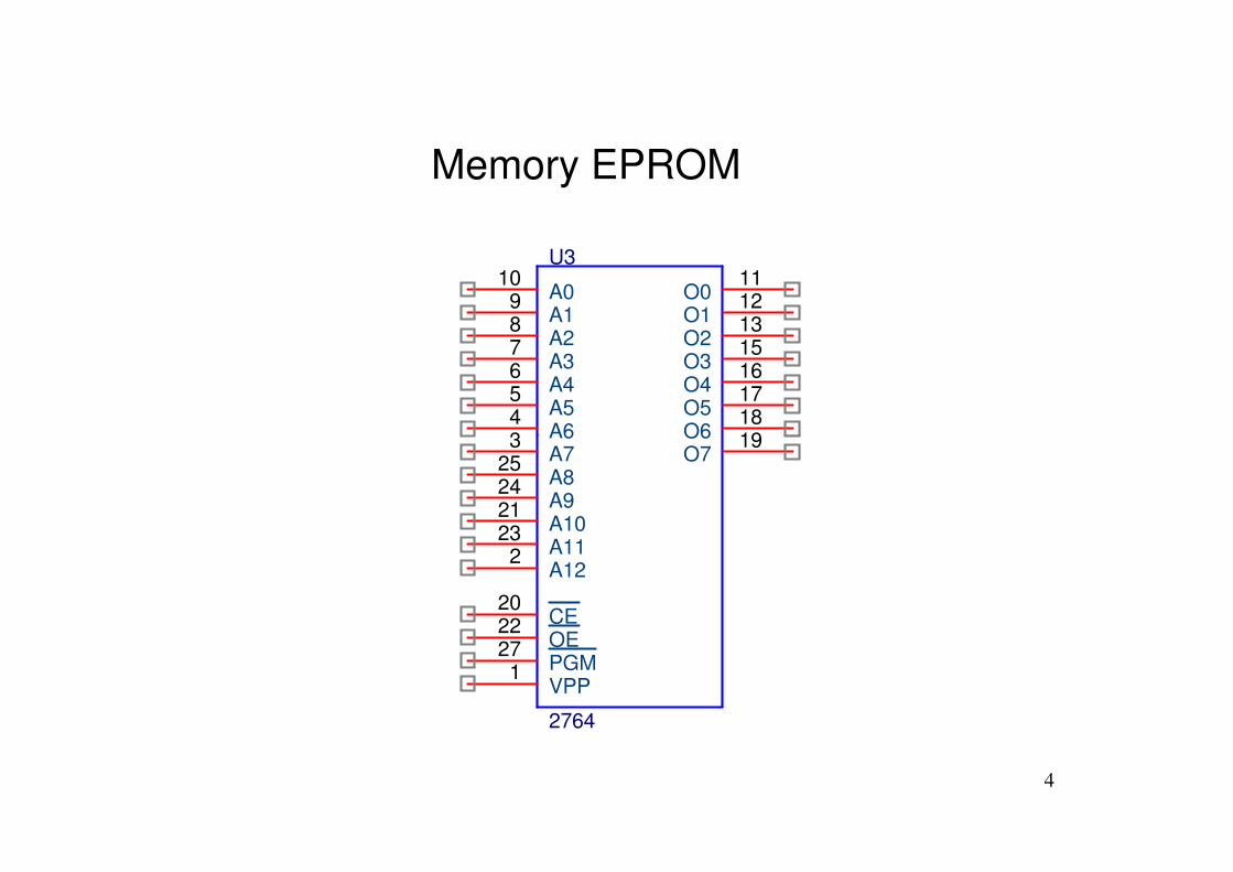
Memory EPROM
U3109876543
1112131516171819
A0A1A2A3A4A5A6
O0O1O2O3O4O5O6
4
2764
3252421232
2022271
19A6A7A8A9A10A11A12
CEOEPGMVPP
O6O7

Memory RAM
U4109876543
1112131516171819
A0A1A2A3A4A5A6
D0D1D2D3D4D5D6
5
HM6264A
3252421232
20262227
19A6A7A8A9A10A11A12
CS1CS2OEWE
D6D7
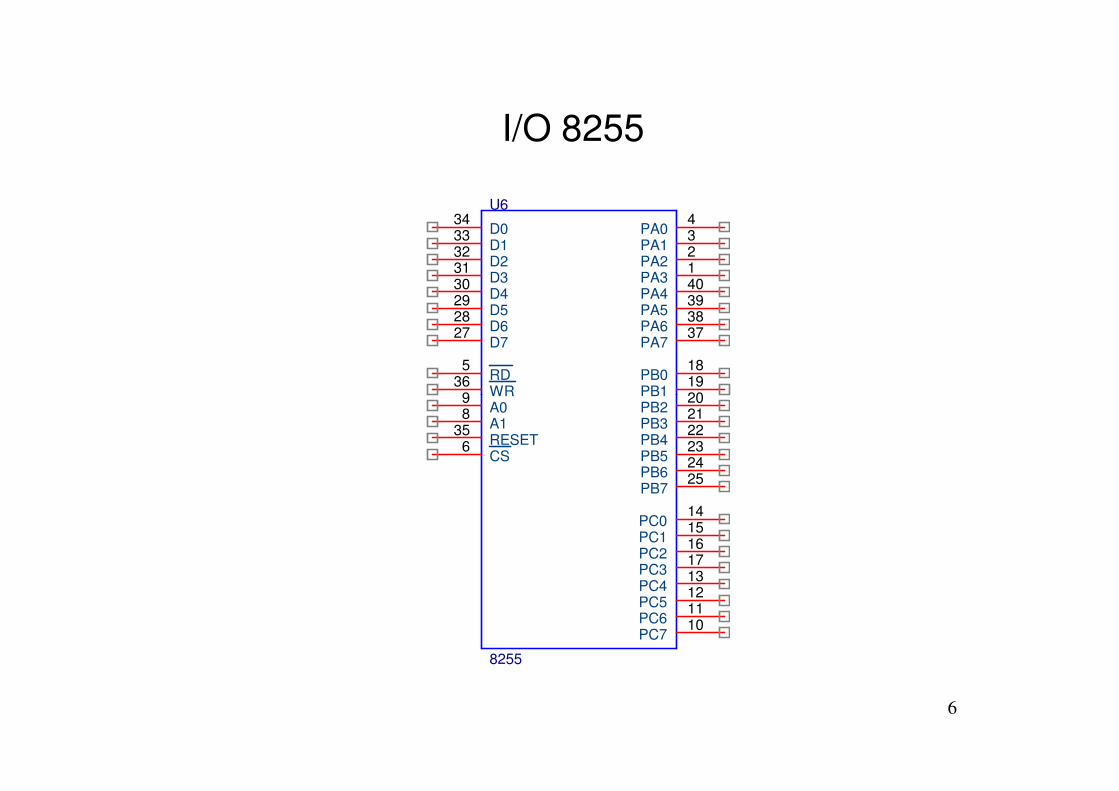
I/O 8255
U63433323130292827
5369
432140393837
181920
D0D1D2D3D4D5D6D7
RDWR
PA0PA1PA2PA3PA4PA5PA6PA7
PB0PB1
6
8255
98
356
202122232425
1415161713121110
WRA0A1RESETCS
PB1PB2PB3PB4PB5PB6PB7
PC0PC1PC2PC3PC4PC5PC6PC7

ROM & RAM Size
• ROM size 8K x 8 bit
13 bit address line A0 - A12
213 = 8192 (0000H - 1FFFH)
7
213 = 8192 (0000H - 1FFFH)
• RAM size 8K x 8 bit
13 bit address line A0 - A12
213 = 8192 (0000H - 1FFFH)

Memory Map
ROM
RAM
0000H
1FFFH2000H
3FFFH4000H
8
Not Used
FFFFH
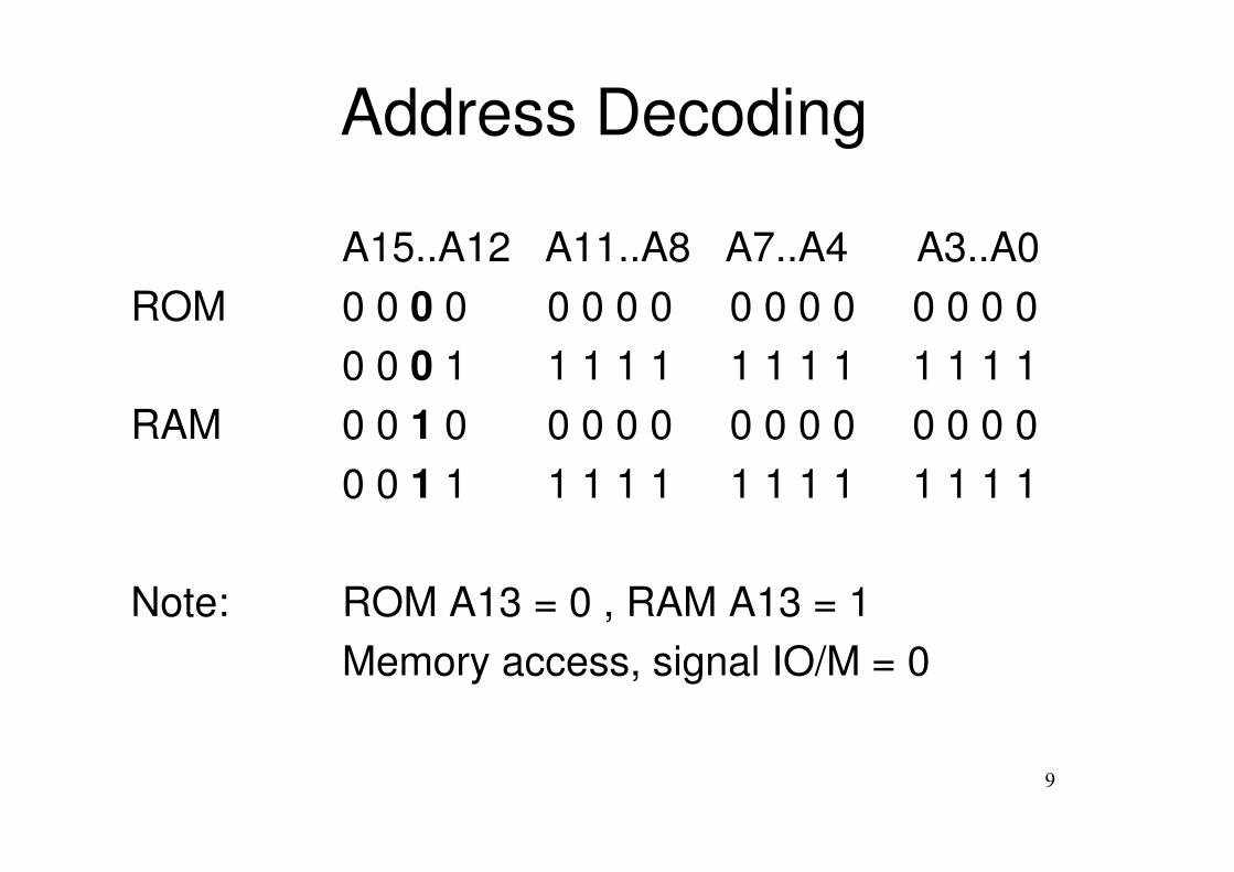
Address Decoding
A15..A12 A11..A8 A7..A4 A3..A0
ROM 0 0 0 0 0 0 0 0 0 0 0 0 0 0 0 0
0 0 0 1 1 1 1 1 1 1 1 1 1 1 1 1
RAM 0 0 1 0 0 0 0 0 0 0 0 0 0 0 0 0
9
RAM 0 0 1 0 0 0 0 0 0 0 0 0 0 0 0 0
0 0 1 1 1 1 1 1 1 1 1 1 1 1 1 1
Note: ROM A13 = 0 , RAM A13 = 1
Memory access, signal IO/M = 0

Implementation of Address Decoders
• Using random logic
Using logic gates such as AND, OR, NOT
and etc.
• Using M-Line to N-Line Decoder
Use existing general decoders such as
10
Use existing general decoders such as
74LS138, 74LS154 and etc.
• Using PAL or FPGA
Using Programmable logic array devices
such as PAL22V10 , PAL16L8 or Field
Programmable Gate Array, ie XILINK.

Memory Decoding Using Random Logic
A14A13
A15ROM CS
OR
11
RAM CS

3 to 8 Decoder
U5123
151413
ABC
Y0Y1Y2
12
74LS138
3
645
1312111097
C
G1G2AG2B
Y2Y3Y4Y5Y6Y7
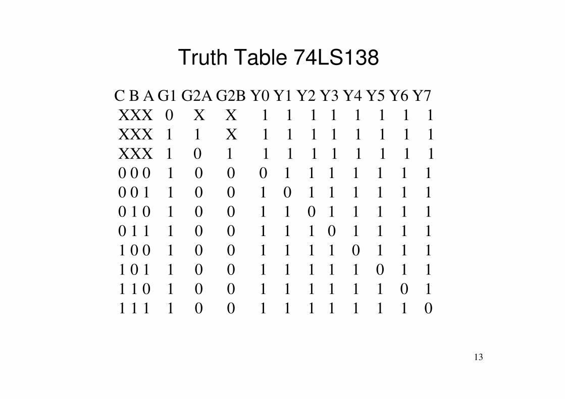
Truth Table 74LS138
C B A G1 G2A G2B Y0 Y1 Y2 Y3 Y4 Y5 Y6 Y7
XXX 0 X X 1 1 1 1 1 1 1 1
XXX 1 1 X 1 1 1 1 1 1 1 1
XXX 1 0 1 1 1 1 1 1 1 1 1
0 0 0 1 0 0 0 1 1 1 1 1 1 1
0 0 1 1 0 0 1 0 1 1 1 1 1 1
13
0 0 1 1 0 0 1 0 1 1 1 1 1 1
0 1 0 1 0 0 1 1 0 1 1 1 1 1
0 1 1 1 0 0 1 1 1 0 1 1 1 1
1 0 0 1 0 0 1 1 1 1 0 1 1 1
1 0 1 1 0 0 1 1 1 1 1 0 1 1
1 1 0 1 0 0 1 1 1 1 1 1 0 1
1 1 1 1 0 0 1 1 1 1 1 1 1 0

Decoder connections
U5123
151413
ABC
Y0Y1Y2
ROM CS
RAM CS
A13
A14
A15
14
74LS138
3
645
1312111097
C
G1G2AG2B
Y2Y3Y4Y5Y6Y7
A15
+5V
IO/M
GND
Not Used
I/O 8255
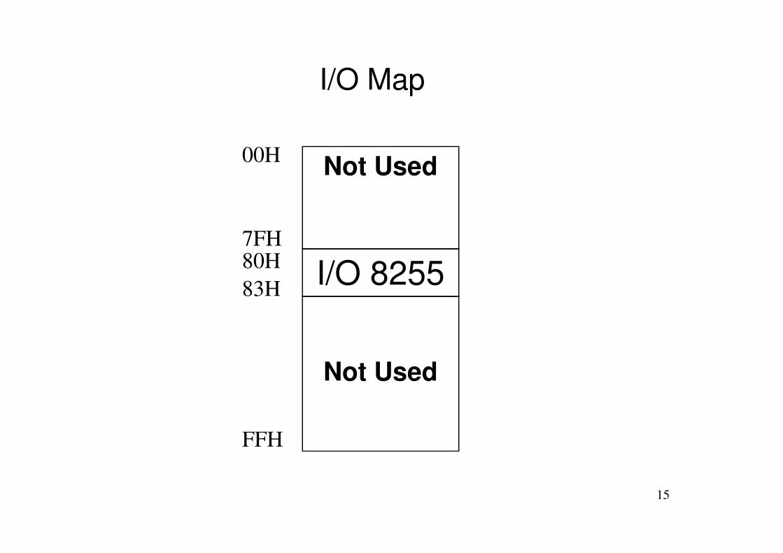
00H
7FH
83H
80H
I/O Map
15
I/O 8255
Not Used
83H
FFH
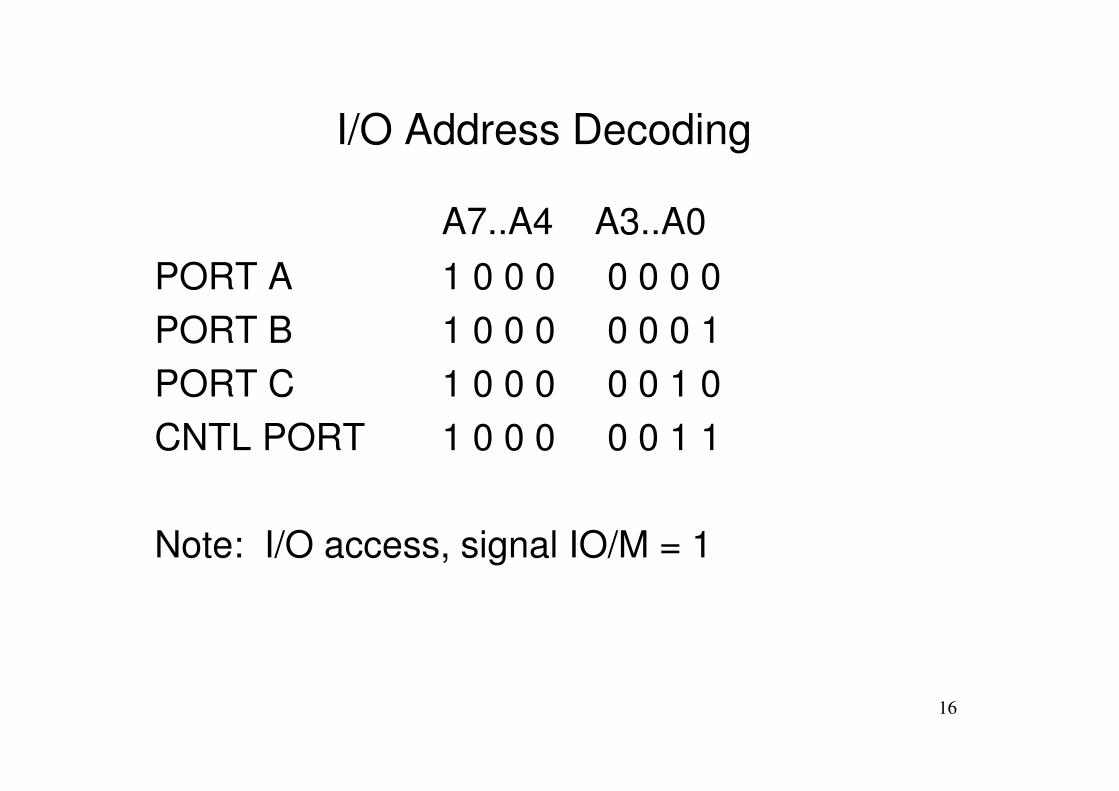
I/O Address Decoding
A7..A4 A3..A0
PORT A 1 0 0 0 0 0 0 0
PORT B 1 0 0 0 0 0 0 1
PORT C 1 0 0 0 0 0 1 0
16
PORT C 1 0 0 0 0 0 1 0
CNTL PORT 1 0 0 0 0 0 1 1
Note: I/O access, signal IO/M = 1

I/O Decoding Using Random Logic
U9
1
2345678
A3
A5
A7
A2
A4
1 2
8255CSA6
17
OR7
8
1 2IO/M

Reset
• Microprocessor must be reset in order to fetch
the first instruction (TR state).
• The microprocessor is automatically reset at
power on by an RC circuit connected to the
18
power on by an RC circuit connected to the
/RESET IN (active low) input of the 8085.
• For proper resetting, the /RESET IN input must
remain at logic 0 for three clock pulses.

Reset Circuit
VCC
R
19
/RESET IN pin 8085microprocessor
SW PUSHBUTTON C
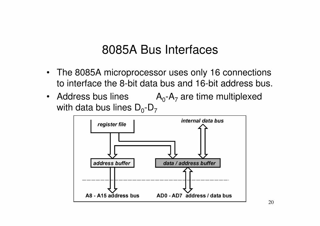
8085A Bus Interfaces
• The 8085A microprocessor uses only 16 connections
to interface the 8-bit data bus and 16-bit address bus.
• Address bus lines A0-A7 are time multiplexed
with data bus lines D0-D7
20
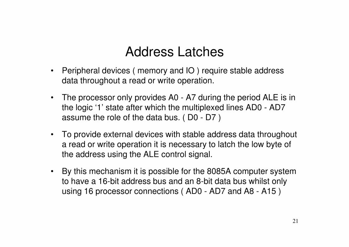
Address Latches
• Peripheral devices ( memory and IO ) require stable address data throughout a read or write operation.
• The processor only provides A0 - A7 during the period ALE is in the logic ‘1’ state after which the multiplexed lines AD0 - AD7 assume the role of the data bus. ( D0 - D7 )
21
• To provide external devices with stable address data throughout a read or write operation it is necessary to latch the low byte of the address using the ALE control signal.
• By this mechanism it is possible for the 8085A computer system to have a 16-bit address bus and an 8-bit data bus whilst only using 16 processor connections ( AD0 - AD7 and A8 - A15 )

De-multiplexing AD0 - AD7
22
Note : See through latches ( eg 74LS573 ) are the preferred type of latch. When clk (ALE) is logic ‘1’ the latch outputs follow the inputs and on the negative edge of clk the data is latched.

De-multiplexing AD0 - AD7
A0
A6
A4
A2
AD0
A3
A7
ADDRESS BUSA5
AD4
AD1
AD6AD7
DATA /ADDRESS BUS AD5
AD2AD3
3478
13141718
256912151619
D0D1D2D3D4D5D6
Q0Q1Q2Q3Q4Q5Q6
A1
23
A7
ALE
AD7
74LS373
18
111
19D6D7
OCG
Q6Q7

U2
74LS373
3478
13141718
111
256912151619
D0D1D2D3D4D5D6D7
OCG
Q0Q1Q2Q3Q4Q5Q6Q7
U3
2764
109876543
252421232
2022271
1112131516171819
A0A1A2A3A4A5A6A7A8A9A10A11A12
CEOEPGMVPP
O0O1O2O3O4O5O6O7
U136
1
2
56
987
10
11
29
33
12131415161718192122232425262728
30313234
RST-IN
X1
X2
SIDTRAP
RST 5.5RST 6.5RST 7.5
INTR
INTA
S0
AD0AD1AD2AD3AD4AD5AD6AD7
A8A9
A10A11A12A13A14A15
ALEWRRD
U63433323130292827
53698
356
432140393837
1819202122232425
141516
D0D1D2D3D4D5D6D7
RDWRA0A1RESETCS
PA0PA1PA2PA3PA4PA5PA6PA7
PB0PB1PB2PB3PB4PB5PB6PB7
PC0PC1
24
U4
HM6264A
109876543
252421232
20262227
1112131516171819
A0A1A2A3A4A5A6A7A8A9A10A11A12
CS1CS2OEWE
D0D1D2D3D4D5D6D7
8085
33
39
35
34337438
S1
HOLD
READY
RDIO/M
RST-OTCLKOSOD
HLDA
8255
161713121110
PC1PC2PC3PC4PC5PC6PC7