Desiggyn For Testability - Yonsei...
44
Design For Testability 2011.06.03 Sungho Kang
Transcript of Desiggyn For Testability - Yonsei...
Design For Testabilityg y
2011.06.03
Sungho Kang
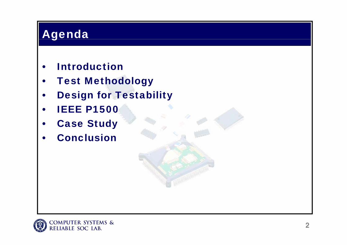
Agendag
• Introduction• Introduction• Test Methodology• Design for Testability• Design for Testability• IEEE P1500• Case Study• Case Study• Conclusion
2
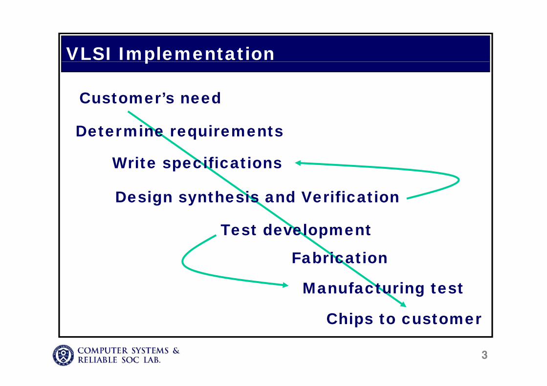
VLSI Implementation
Customer’s need
p
Determine requirements
Write specifications
D i th i d V ifi tiDesign synthesis and Verification
Test development
Fabrication
p
Manufacturing test
Chips to customer
3
p
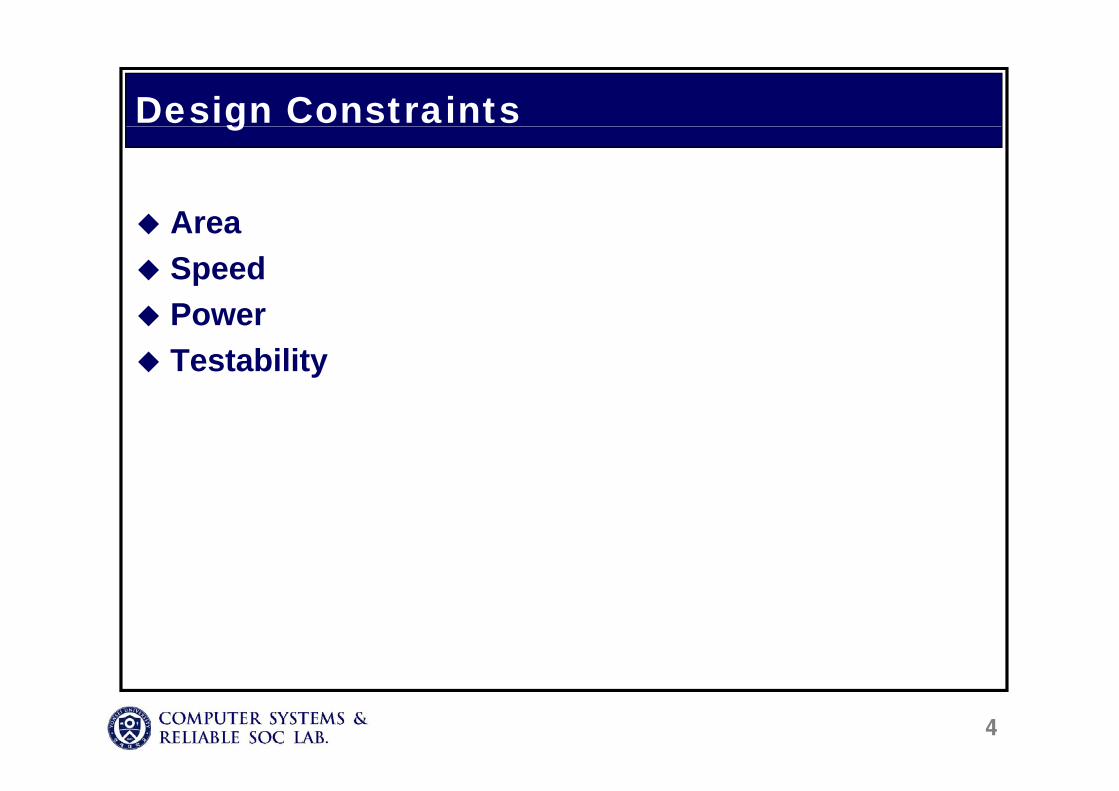
Design Constraints g
AAreaSpeedPPower Testability
4
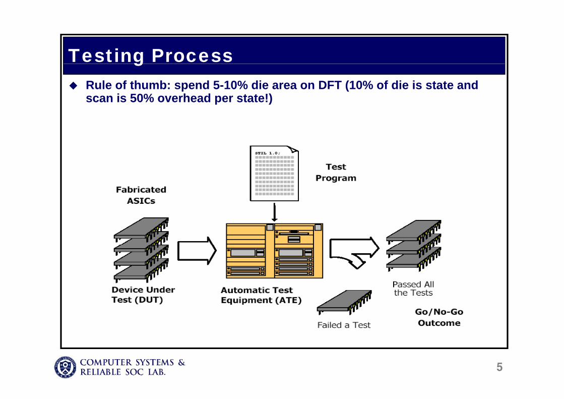
Testing ProcessgRule of thumb: spend 5-10% die area on DFT (10% of die is state and scan is 50% overhead per state!)
5

SOC Designg
User DefinedCore
IP
ROM
User Defined
Core DRAMUDL
IO P
ad
IO P
ad
RF/AnalogCore
IP
IP
6
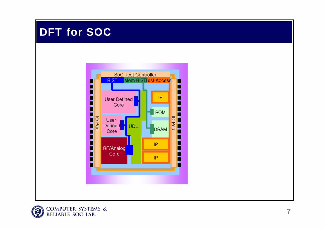
DFT for SOC
BIST Mem BISTTest AccessSoC Test Controller
User DefinedCore
IP
ROM
User Defined
Core DRAMUDL
IO P
ad
IO P
ad
RF/AnalogCore
IP
IP
7
Manufacturing Defectsg
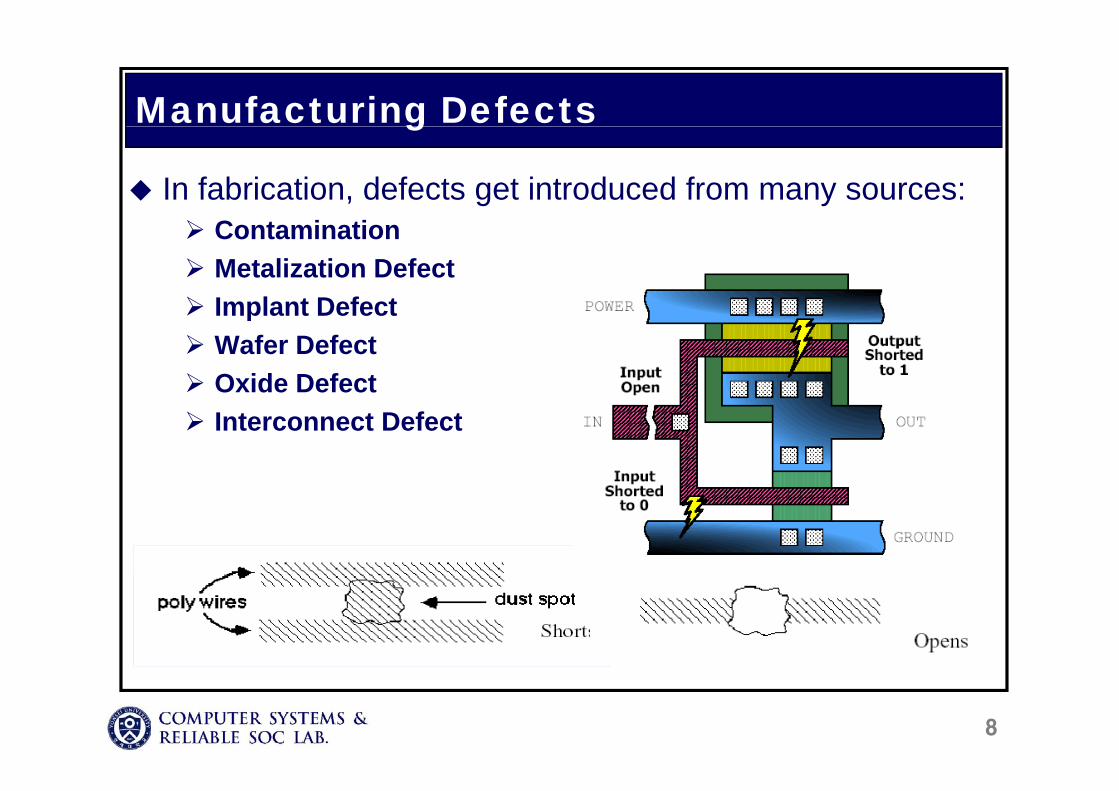
In fabrication, defects get introduced from many sources:ContaminationMetalization DefectImplant DefectImplant DefectWafer DefectOxide DefectInterconnect Defect
8
Defect & Fault
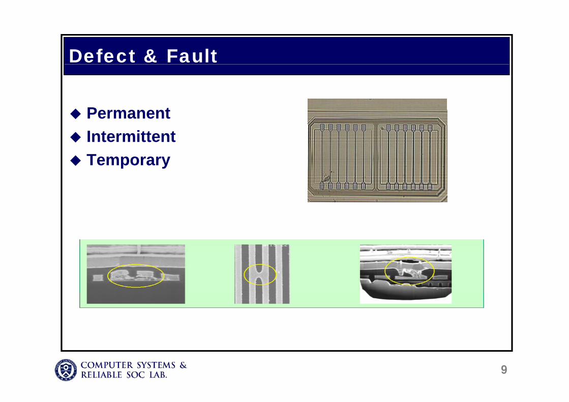
P tPermanentIntermittentTTemporary
9

Clustered VLSI Defects
Good chips
Faulty chips
WaferDefects
Unclustered defectsWafer yield = 12/22 = 0.55
Clustered defects (VLSI)Wafer yield = 17/22 = 0.77
10
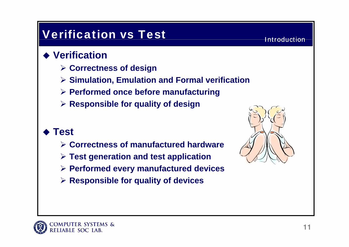
Verification vs Test IntroductionIntroduction
VerificationCorrectness of design
IntroductionIntroduction
Correctness of designSimulation, Emulation and Formal verificationPerformed once before manufacturinggResponsible for quality of design
TestCorrectness of manufactured hardwareTest generation and test applicationPerformed every manufactured devicesResponsible for quality of devicesResponsible for quality of devices
11
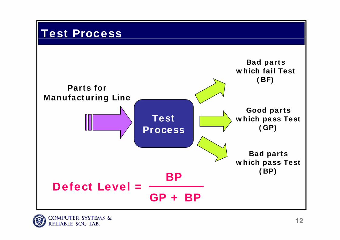
Test Process
Bad parts
Parts for
pwhich fail Test
(BF)
Test
Manufacturing Line
Good partswhich pass TestTest
Processwhich pass Test
(GP)
Bad partswhich pass Test
(BP)BP
( )
Defect Level =BP
GP + BP
12
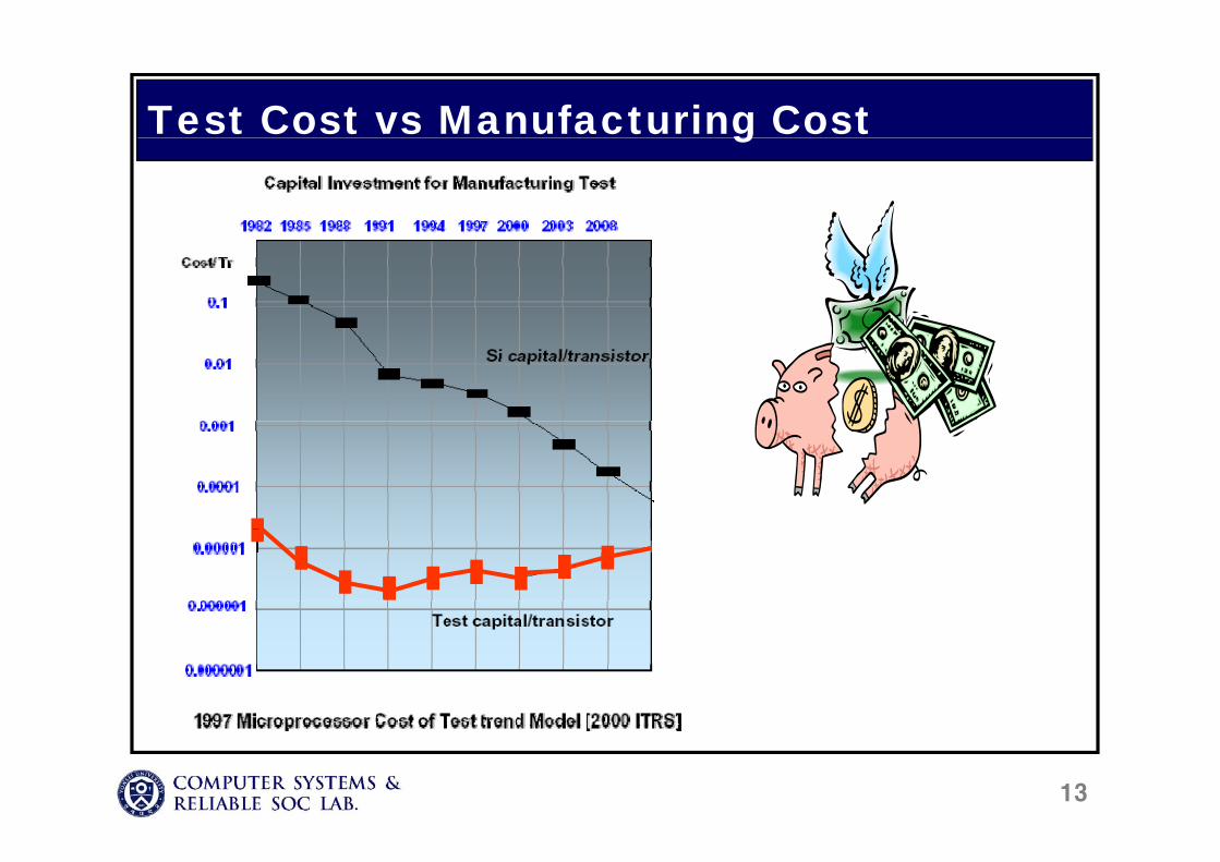
Test Cost vs Manufacturing Costg
13
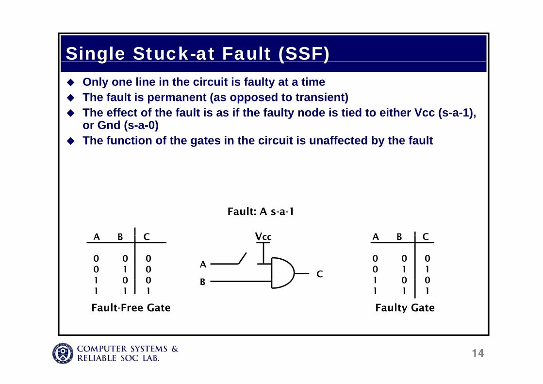
Single Stuck-at Fault (SSF)g ( )Only one line in the circuit is faulty at a timeThe fault is permanent (as opposed to transient)The effect of the fault is as if the faulty node is tied to either Vcc (s-a-1), or Gnd (s-a-0)The function of the gates in the circuit is unaffected by the fault
A B C Vcc
Fault: A s-a-1
A B CA B C
0 0 00 1 01 0 0
Vcc
A
BC
A B C
0 0 00 1 11 0 01 0 0
1 1 1
Fault-Free Gate
B 1 0 01 1 1
Faulty Gate
14
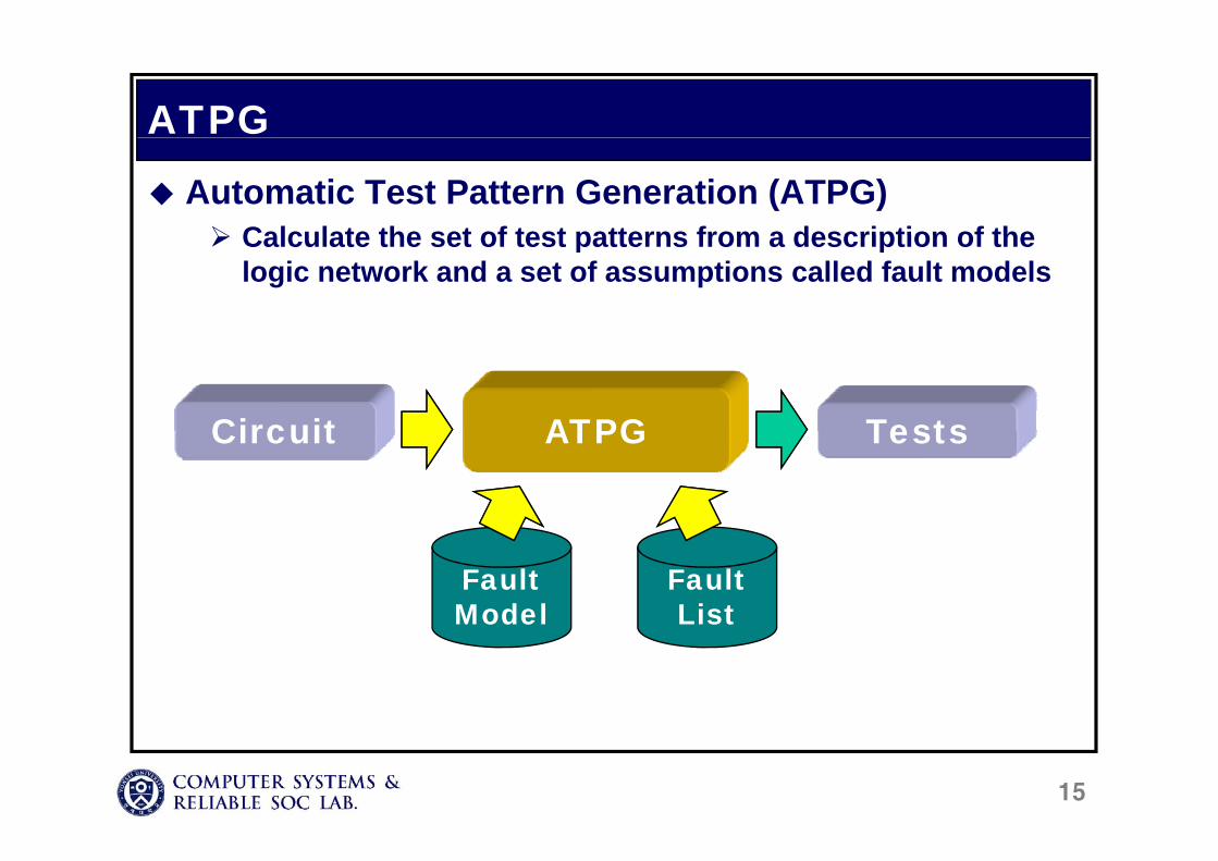
ATPGAutomatic Test Pattern Generation (ATPG)
Calculate the set of test patterns from a description of theCalculate the set of test patterns from a description of the logic network and a set of assumptions called fault models
ATPGCircuit TestsATPGCircuit Tests
FaultList
FaultModel
15
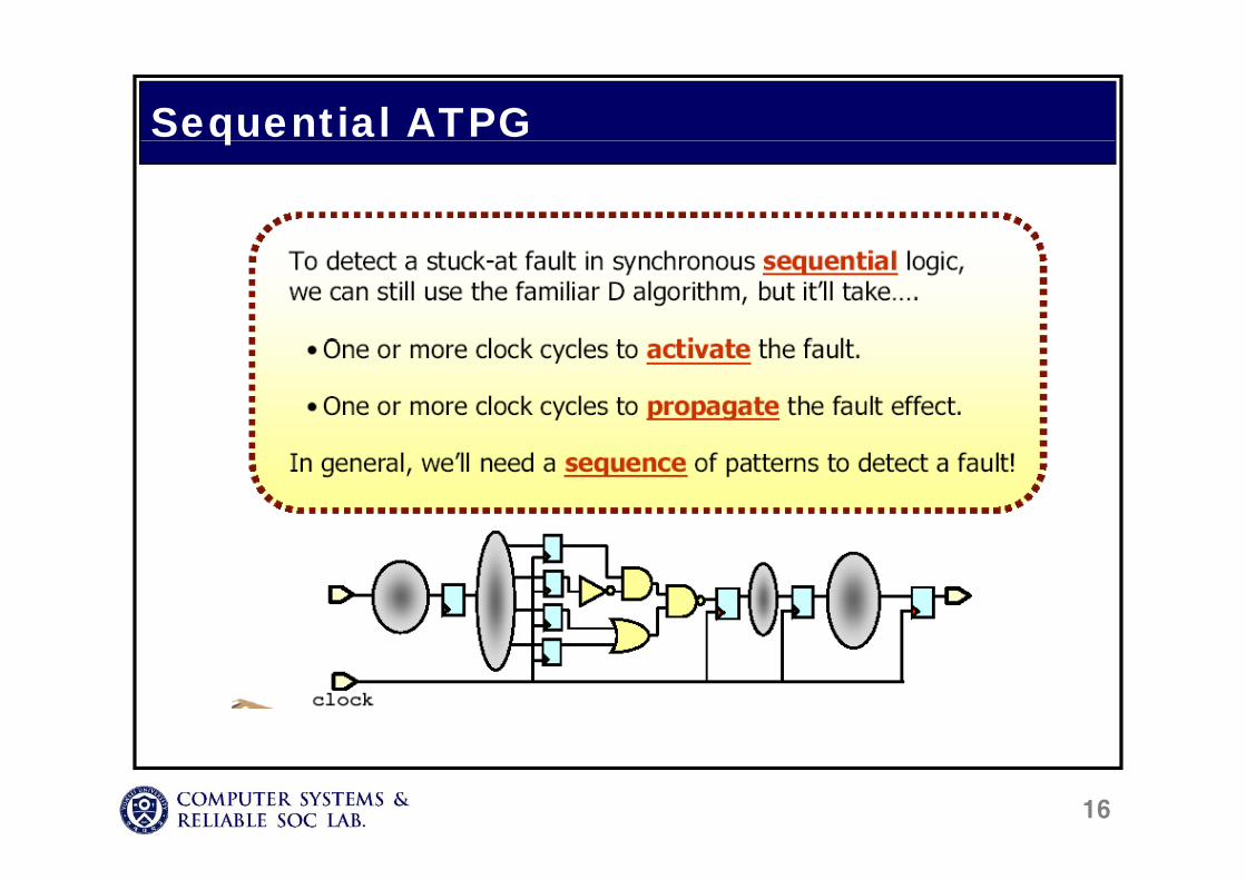
Sequential ATPGq
16

Design-for-Testability (DFT)g y ( )Definition
Any design effort to reduce test costsAny design effort to reduce test costsThe process of including special features to make a device easily testable
ObjectiveTo reduce in overall design cycle times and test costs
ith t ifi i th lit f th d twithout sacrificing the quality of the product
17

DFT Flow
Verilog/VHDL Netlist
DFT Rule CheckingDFT Rule Checking
g
Scan Design, Boundary Scan DesignMemory BIST Design, Logic BIST DesignTest Synthesis y g , g g
DFT Rule CheckingStatic Timing AnalysisDFT Rule Checking
Test Pattern GenerationATPG
Logic SimulationTest Vector TranslationFull Timing Simulation
18
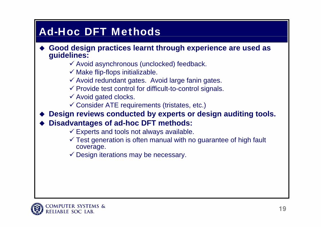
Ad-Hoc DFT MethodsGood design practices learnt through experience are used as guidelines:
A id h ( l k d) f db kAvoid asynchronous (unclocked) feedback.Make flip-flops initializable.Avoid redundant gates. Avoid large fanin gates.Provide test control for difficult to control signalsProvide test control for difficult-to-control signals.Avoid gated clocks.Consider ATE requirements (tristates, etc.)
Design reviews conducted by experts or design auditing toolsDesign reviews conducted by experts or design auditing tools.Disadvantages of ad-hoc DFT methods:
Experts and tools not always available.Test generation is often manual with no guarantee of high faultTest generation is often manual with no guarantee of high fault coverage.Design iterations may be necessary.
19

Test PointsEmploy test points to enhance controllability and observabilityobservabilityLarge demand on extra I/O pins ExampleExample
20
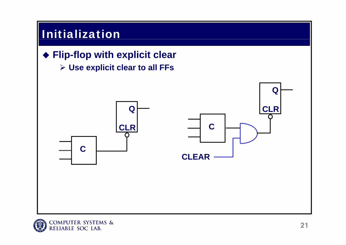
InitializationFlip-flop with explicit clear
Use explicit clear to all FFsUse explicit clear to all FFs
Q
Q CLR
CLR
C
C
CCLEAR
21

PartitioninggSplit large counters
22
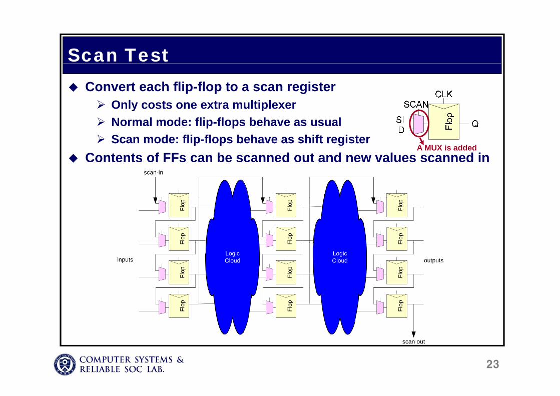
Scan TestConvert each flip-flop to a scan register
Only costs one extra multiplexerOnly costs one extra multiplexerNormal mode: flip-flops behave as usualScan mode: flip-flops behave as shift register
C t t f FF b d t d l d iA MUX is added
Contents of FFs can be scanned out and new values scanned inscan-in
Flop
Flop
Flop
Flop
Flop
Flop
inputs outputs
FFl
op
FFl
op
FFl
op
LogicCloud
LogicCloud
Flop
Flop
Flop
23
scan out
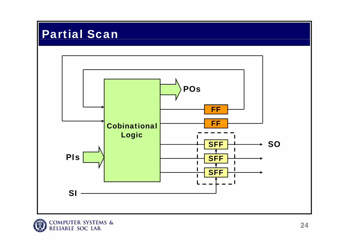
Partial Scan
POs
FF
FFCobinationalLogic
FF
SFF SOPIs SFF
SFF
SI
24
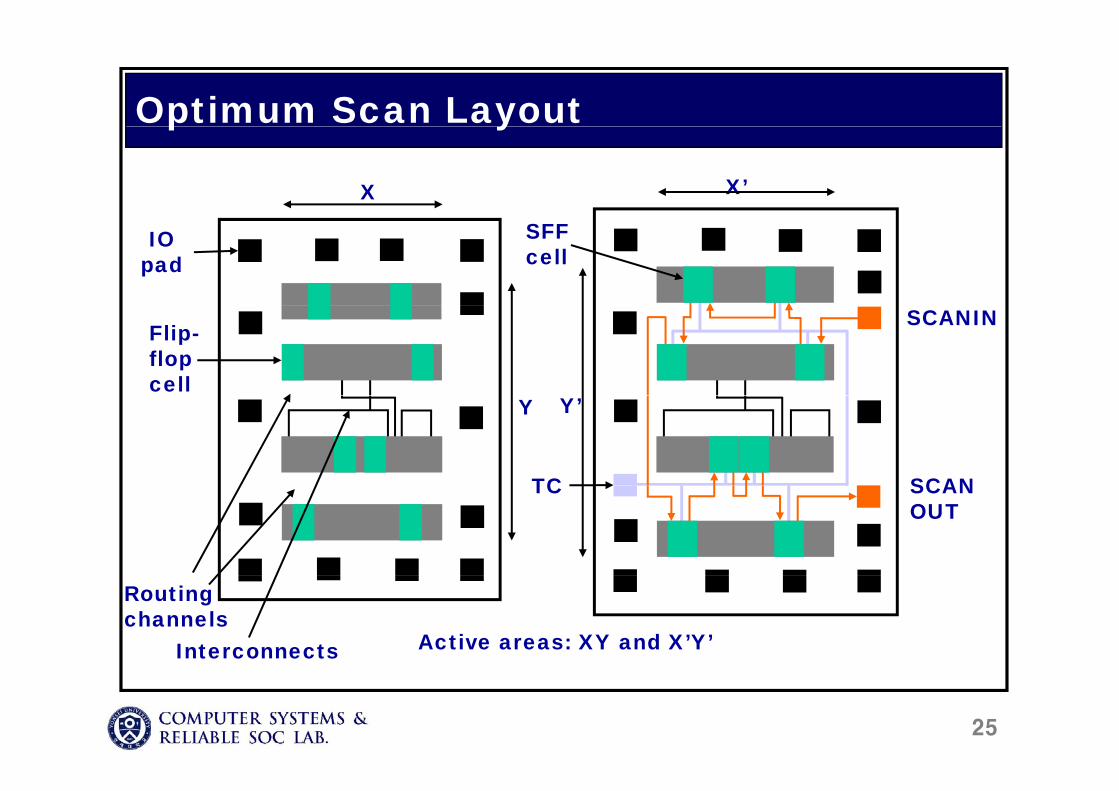
Optimum Scan Layoutp y
X’X
IOpad
SFFcell
Flip-flopcell
SCANIN
TC SCAN
Y Y’
TC SCANOUT
Interconnects
Routingchannels
Active areas: XY and X’Y’
25
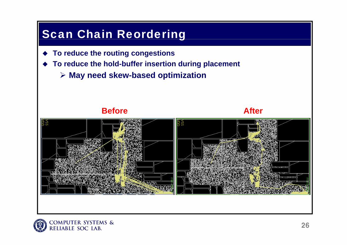
Scan Chain ReorderinggTo reduce the routing congestionsTo reduce the hold-buffer insertion during placementg p
May need skew-based optimization
Before After
26

Logic BISTg
Pseudo-RandomPattern Generator
PRPG
Pattern Generator
Logic BISTcontroller
Scan ch
Scan ch
Scan ch
Scan chControl unit
All flops placedinto large number of
relatively shortcontroller hain
hain
hain
hain
Control unitsequences all
activityscan chains
MISR
Multiple Input Signature Registercompresses responses into a signature
27
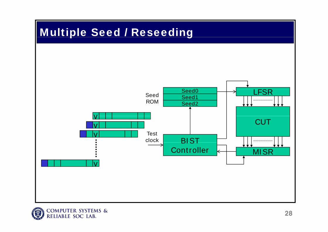
Multiple Seed / Reseedingp g
LFSRSeed0 LFSRSeed0Seed1Seed2
SeedROM
vCUT
BISTTestclock
vvv
MISRBIST
Controller
v
28

Bit Fixing/Bit Flipping Methodg pp g
t0 t1 … ... tL-1 s0 s1 … ... sn-1
Scan chain
SignatureAnalyzer
… ...
SequentialCUT
Bit FlippingCircuit
29
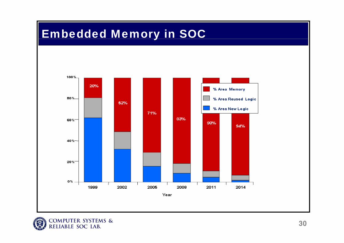
Embedded Memory in SOCy
30
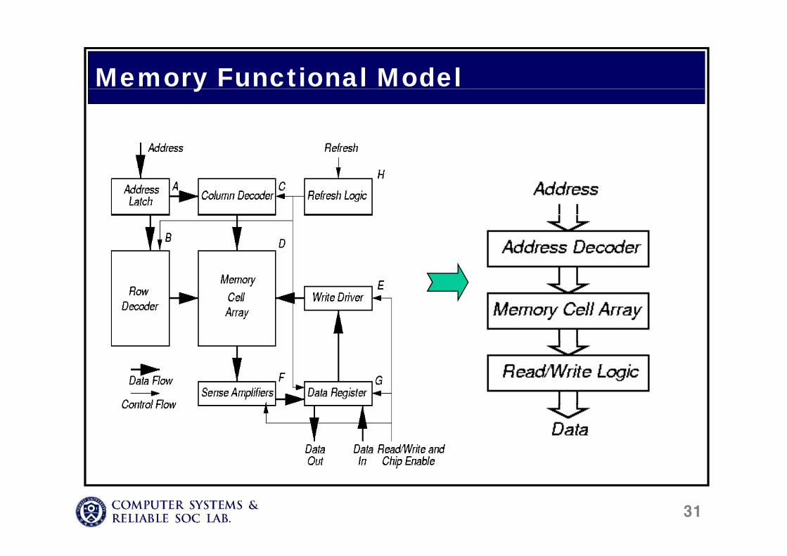
Memory Functional Modely
31
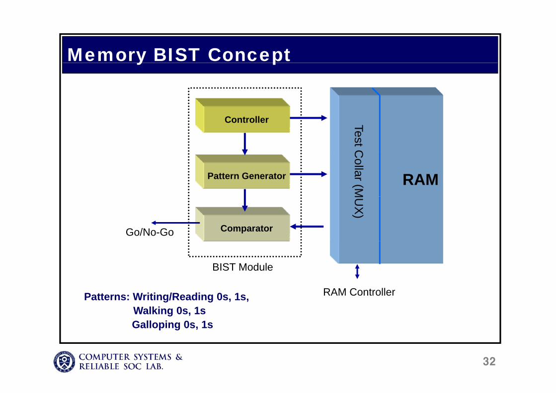
Memory BIST Concepty p
Controller Test C
Pattern Generator RAMC
ollar (M
Comparator
MU
X)
Go/No-Go
BIST Module
RAM ControllerPatterns: Writing/Reading 0s, 1s,Walking 0s, 1sGalloping 0s, 1s
32
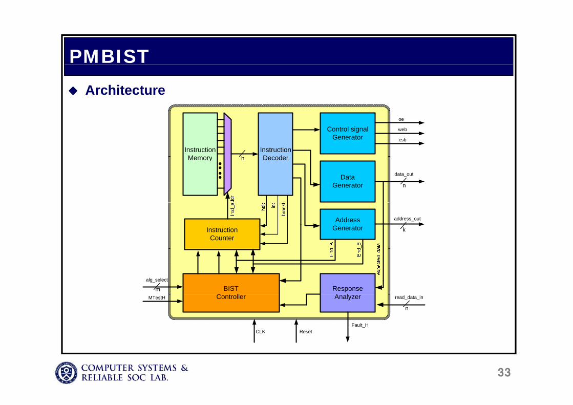
PMBIST Architecture
InstructionDecoder
InstructionMemory
Control signalGenerator
oe
web
csb
h
Data Generator
DecoderMemory
data_out
n
h
InstructionCounter
Address Generator k
address_out
ResponseA l
BISTC t ll
alg_select
mAnalyzer read_data_in
ResetCLK
ControllerMTestH
n
Fault_H
33

Built-In Redundancy Analysis (BIRA)y y ( )메모리셀의고장을분석하고여분의셀을이용해고장을수리하기위한효율적인방법을찾고자함
수리비용및시간의단축을위하여 redundancy analysis 방식을 built-in하여메모리셀을수리 Hardware overhead 및 repair rate의고려가필요성능평가기준: repair rate, area overhead, rate of overused spares,성능평가기준: repair rate, area overhead, rate of overused spares, analysis sped
고장 수리 전 메모
리
고장 수리 후 메모
리
34

Test Compression Compress the test input sequencesN d d i it t k i i l t t
p
Need a decompression units to make original test sequencesCan be reduced for both limitations of ATECan be reduced for both limitations of ATE
The size of ATE memoryThe width of ATE channel
Can be reduced test application time
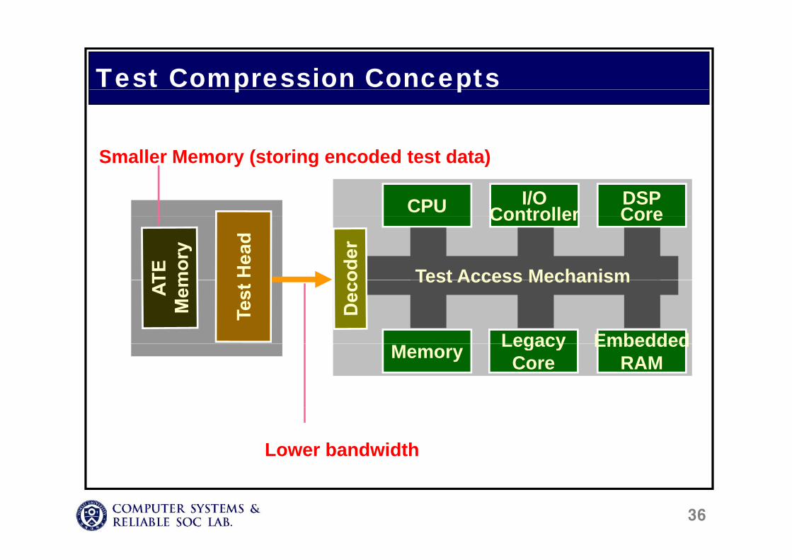
Test Compression Concepts
S ll M ( t i d d t t d t )
p p
CPU I/OController
DSPCore
Smaller Memory (storing encoded test data)
Controller Core
Test Access Mechanism
Legacy Embedded
Test Access Mechanism
Memory LegacyCore
EmbeddedRAM
Lower bandwidth
36
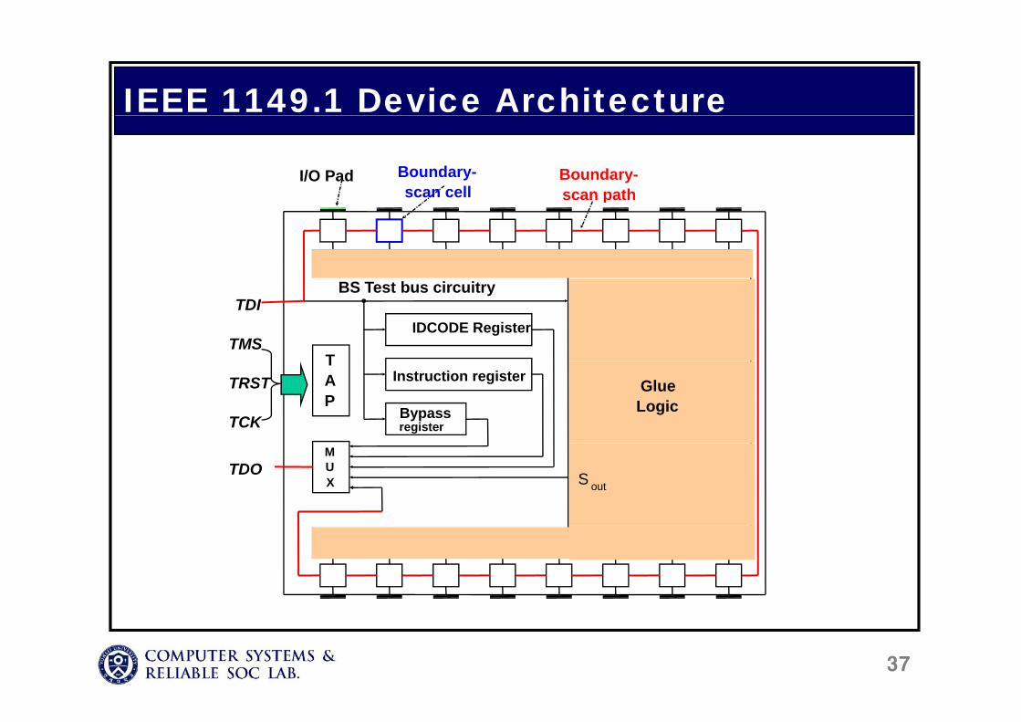
IEEE 1149.1 Device Architecture
I/O Pad Boundary-scan cell
Boundary-scan pathscan cell scan path
IDCODE Register
T
BS Test bus circuitryTDI
TMS
Instruction register
Bypassregister
TAP
TCK
GlueLogic
TRST
MUX
TDO S out
37
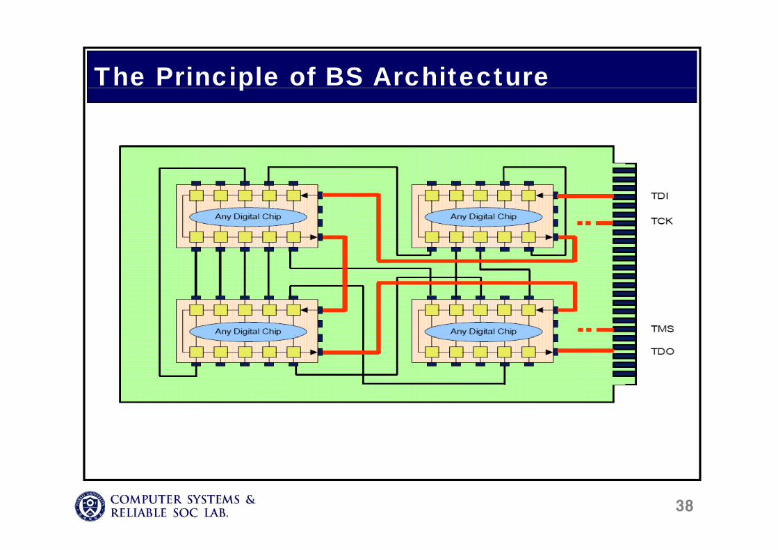
The Principle of BS Architecturep
38
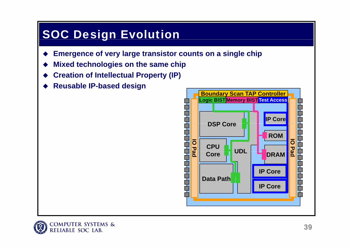
SOC Design EvolutiongEmergence of very large transistor counts on a single chipMixed technologies on the same chipg pCreation of Intellectual Property (IP)Reusable IP-based design
Boundary Scan TAP Controller
DSP CoreIP Core
Logic BIST Memory BIST T̀est AccessBoundary Scan TAP Controller
CPU
DSP Core
ROM
UDLIO
Pa
IO Pa
Data Path
Core DRAM
IP Core
UDLad ad
Data PathIP Core
39
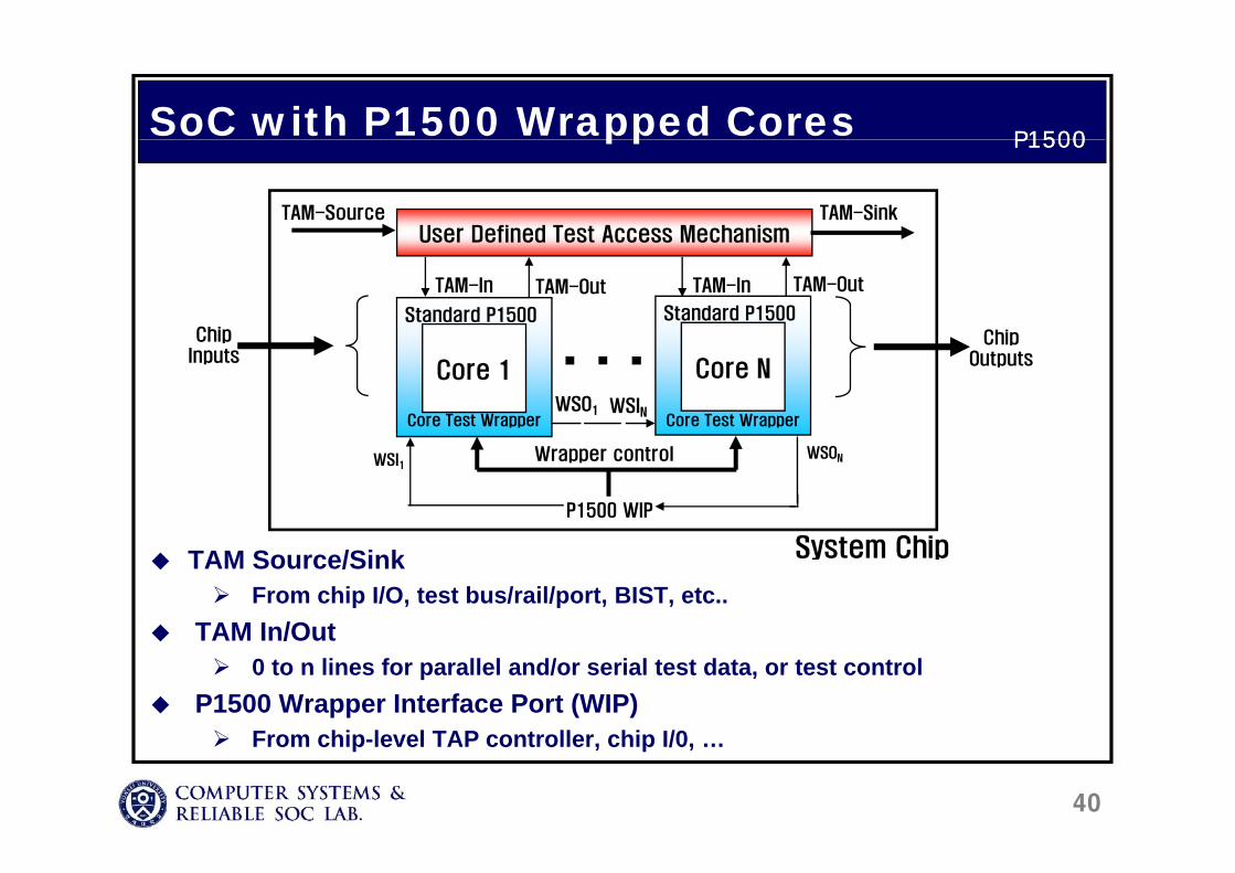
SoC with P1500 Wrapped Cores P1500P1500pp
User Defined Test Access MechanismTAM-Source TAM-Sink
P1500P1500
Chip
User Defined Test Access Mechanism
Standard P1500 Standard P1500
TAM-In TAM-InTAM-Out TAM-Out
Chip ChipOutputs
Core 1
Core Test Wrapper
Core N
Core Test WrapperWSO1 WSIN
ChipInputs
P1500 WIP
Wrapper controlWSI1WSON
S ChiSystem ChipTAM Source/SinkFrom chip I/O, test bus/rail/port, BIST, etc..
TAM In/OutTAM In/Out0 to n lines for parallel and/or serial test data, or test control
P1500 Wrapper Interface Port (WIP)F hi l l TAP t ll hi I/0
40
From chip-level TAP controller, chip I/0, …
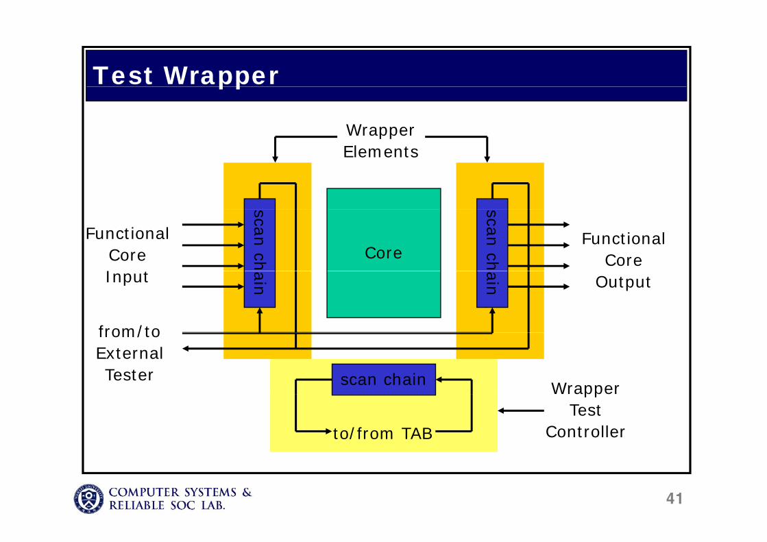
Test Wrapperpp
WrapperElementElements
Core
scan ch
scan ch
FunctionalCoreI t
FunctionalCoreain
ain
from/to
Input Output
scan chain
from/toExternalTester
Wrapper
to/from TAB
appeTest
Controller
41
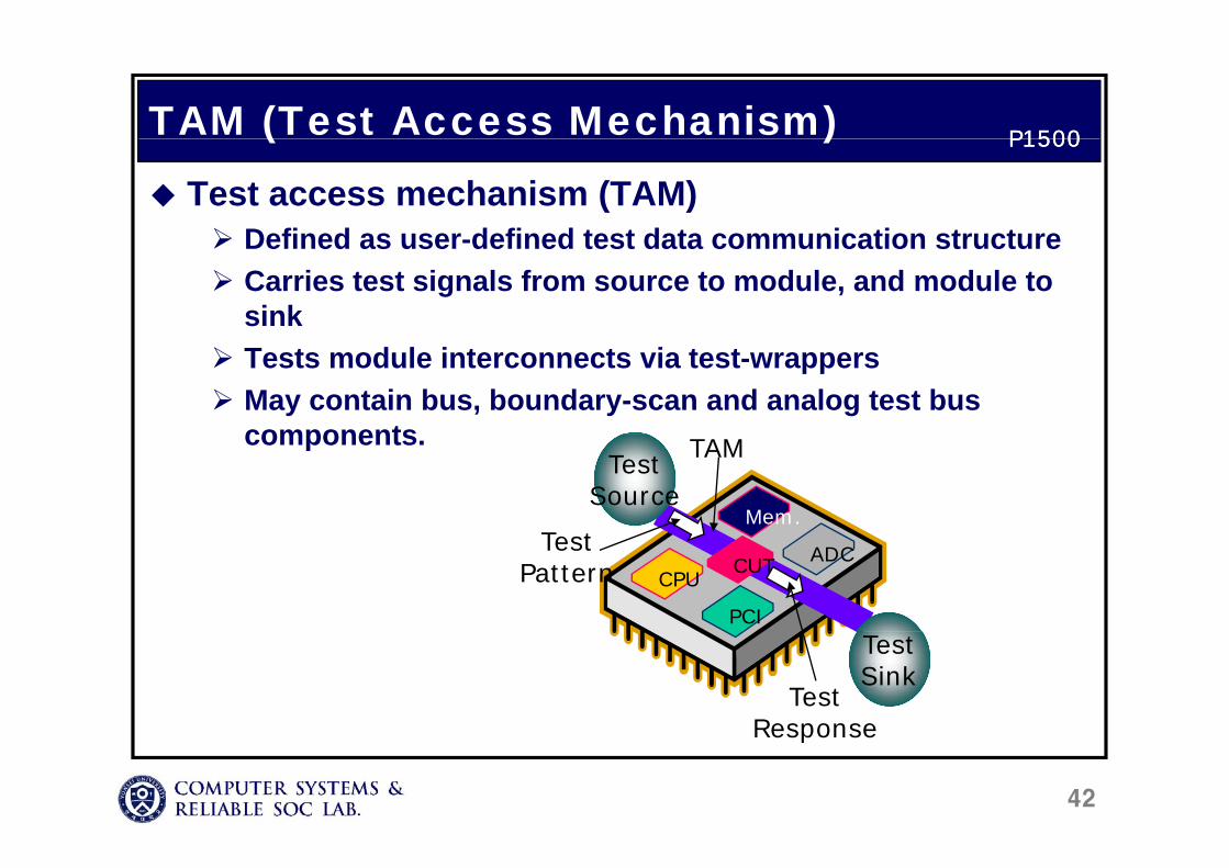
TAM (Test Access Mechanism) P1500P1500( )Test access mechanism (TAM)
Defined as user defined test data communication structure
P1500P1500
Defined as user-defined test data communication structureCarries test signals from source to module, and module to sinkTests module interconnects via test-wrappersMay contain bus, boundary-scan and analog test bus componentscomponents.
Mem.
TAMTest
Source
T tCPU
ADC
PCI
CUTTest
Pattern
TestSink
TestResponse
42
Response
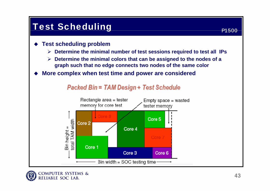
Test Scheduling P1500P1500g
Test scheduling problemDetermine the minimal number of test sessions required to test all IPs
P1500P1500
Determine the minimal number of test sessions required to test all IPsDetermine the minimal colors that can be assigned to the nodes of a graph such that no edge connects two nodes of the same color
More complex when test time and power are consideredMore complex when test time and power are considered
43

Conclusion• Testable core design• Logic BIST• Test reuse
• Core access architecture• Parallel access & bypass• Core isolation
• IP-system test interface
BIST Mem BISTTest AccessSoC Test Controller
• Hierarchical testingCore isolation
• Automatic test pattern • Fault simulation
Test Automation
User DefinedCore
IP
ROM
• Test spec.• Test hardware
control
Fault simulation• Testability measure• Scan insertion & synthesis
• BIST circuit synthesisUser
DefinedCore DRAM
UDL
IO P
ad
IO P
ad
control• Test
scheduling
BIST circuit synthesis• Boundary scan insertion & synthesis
RF/AnalogCore
IP
IP
Low costexternal ATE
• Memory test algorithmM BIST BISR
• Testable design
• Analog Fault modeling• Mixed signal Built-In Self Test
• Built-In Self Calibration
44
• Memory BIST, BISR• Built In Self Calibration