Description - Fujitsu Global€¦ · Austin, TX 78730-1156 February 2016 Ambiq Micro Apollo MCU...
384
Apollo Datasheet Ultra-Low Power MCU Family Ambiq Micro Inc. 6500 River Place Blvd., Bldg. 7, Ste. 200 2016 Ambiq Micro, Inc. www.ambiqmicro.com Austin, TX 78730-1156 February 2016 Ambiq Micro Apollo MCU Host Processor (optional) SPI/I 2 C Slave Port SPI/I 2 C Master, UART Radio Magnetometer with Digital Output Gyroscope with Digital Output Accelerometer with Digital Output Typical Sensor Application Circuit for the Apollo MCU Features Ultra-low supply current: - EEMBC ULPBench score of 377 - 35 µA/MHz executing from flash at 3.3 V - 143 nA deep sleep mode at 3.3 V - 419 nA deep sleep mode with XTAL-assisted RTC at 3.3 V High-performance ARM Cortex-M4F Processor - Up to 24 MHz clock frequency - Floating point unit - Memory protection unit Wake-up interrupt controller with 12 interrupts Ultra-low power memory: - Up to 512 KB of flash memory for code/data - Up to 64 KB of low leakage RAM for code/data Ultra-low power interface for off-chip sensors: - 10 bit, 13-channel, up to 800 kSps ADC - Temperature sensor with +/-4ºC accuracy Flexible serial peripherals: -I 2 C/SPI master for communication with sensors, radios, and other peripherals -I 2 C/SPI slave for host communications - UART for communication with peripherals and legacy devices Rich set of clock sources: - 32.768 kHz XTAL oscillator - Low frequency RC oscillator – 1.024 kHz - High frequency RC oscillator – 24 MHz - RTC based on Ambiq’s AM08X5/18X5 families Wide operating range: 1.8-3.8 V, –40 to 85°C Compact package options: - 2.49 x 2.90 mm 41-pin CSP with 27 GPIO - 4.5 x 4.5 mm 64-pin BGA with 50 GPIO Applications - Wearable electronics - Wireless sensors - Activity and fitness monitors - Consumer electronics - Consumer medical devices - Smart watches Description The Apollo MCU family is an ultra-low power, highly integrated microcontroller designed for battery- powered devices including wearable electronics, activity & fitness monitors, and wireless sensors. By combining ultra-low power sensor conversion electronics with the powerful ARM Cortex-M4F processor, the Apollo MCU enables complex sensor processing tasks to be completed with unprecedented battery life. Weeks, months, and years of battery life are achievable while doing complex context detection, gesture recognition, and activity monitoring. The Apollo MCU takes full advantage of Ambiq Micro’s patented Subthreshold Power Optimized Technology (SPOT) Platform, setting a new industry benchmark in low power design. The Apollo MCU also integrates up to 512 KB of flash memory and 64 KB of RAM to accommodate radio and sensor overhead while still leaving plenty of space for application code. This microcontroller also includes a serial master and UART port for communicating with radios and sensors including accelerometers, gyroscopes, and magnetometers.
Transcript of Description - Fujitsu Global€¦ · Austin, TX 78730-1156 February 2016 Ambiq Micro Apollo MCU...

Apollo Datasheet
Ultra-Low Power MCU Family
FeaturesUltra-low supply current:
- EEMBC ULPBench score of 377- 35 µA/MHz executing from flash at 3.3 V- 143 nA deep sleep mode at 3.3 V- 419 nA deep sleep mode with XTAL-assisted
RTC at 3.3 V
High-performance ARM Cortex-M4F Processor
- Up to 24 MHz clock frequency- Floating point unit- Memory protection unit
Wake-up interrupt controller with 12 interrupts
Ultra-low power memory:
- Up to 512 KB of flash memory for code/data- Up to 64 KB of low leakage RAM for code/data
Ultra-low power interface for off-chip sensors:
- 10 bit, 13-channel, up to 800 kSps ADC- Temperature sensor with +/-4ºC accuracy
Flexible serial peripherals:
- I2C/SPI master for communication with sensors, radios, and other peripherals
- I2C/SPI slave for host communications- UART for communication with peripherals and
legacy devices
Rich set of clock sources:
- 32.768 kHz XTAL oscillator- Low frequency RC oscillator – 1.024 kHz- High frequency RC oscillator – 24 MHz- RTC based on Ambiq’s AM08X5/18X5 families
Wide operating range: 1.8-3.8 V, –40 to 85°C
Compact package options:
- 2.49 x 2.90 mm 41-pin CSP with 27 GPIO- 4.5 x 4.5 mm 64-pin BGA with 50 GPIO
A------
DThintpoaccoeleproprounyecoacadPosede
Thflaradof alscoac
Ambiq Micro Inc. 6500 River Place Bwww.ambiqmicro.com Austin, TX
Host
Processor
(optional)
SPI/ISlavPor
Radio
Magnet
with D
Out
Typical Sensor Applicat
pplicationsWearable electronicsWireless sensorsActivity and fitness monitorsConsumer electronicsConsumer medical devicesSmart watches
escriptione Apollo MCU family is an ultra-low power, highlyegrated microcontroller designed for battery-wered devices including wearable electronics,tivity & fitness monitors, and wireless sensors. Bymbining ultra-low power sensor conversionctronics with the powerful ARM Cortex-M4Fcessor, the Apollo MCU enables complex sensorcessing tasks to be completed with
precedented battery life. Weeks, months, andars of battery life are achievable while doingmplex context detection, gesture recognition, andtivity monitoring. The Apollo MCU takes fullvantage of Ambiq Micro’s patented Subthresholdwer Optimized Technology (SPOT) Platform,tting a new industry benchmark in low powersign.
e Apollo MCU also integrates up to 512 KB ofsh memory and 64 KB of RAM to accommodateio and sensor overhead while still leaving plentyspace for application code. This microcontrollero includes a serial master and UART port formmunicating with radios and sensors includingcelerometers, gyroscopes, and magnetometers.
lvd., Bldg. 7, Ste. 200 2016 Ambiq Micro, Inc. 78730-1156 February 2016
Ambiq Micro
Apollo
MCU
2C e t
SPI/I2C Master,UART
ometer
igital
put
Gyroscope
with Digital
Output
Accelerometer
with Digital
Output
ion Circuit for the Apollo MCU

Apollo Datasheet
7
Contents1. Package Pins ..................................................................................................... 23
1.1 Pin Configuration ......................................................................................... 231.2 Pin Connections .......................................................................................... 24
2. System Core ...................................................................................................... 32
3. MCU Core Details .............................................................................................. 33
3.1 Interrupts And Events .................................................................................. 343.2 Memory Map ................................................................................................ 353.3 Memory Protection Unit (MPU) .................................................................... 363.4 System Busses ............................................................................................ 373.5 Power Management .................................................................................... 37
3.5.1 Cortex M4F Power Modes .................................................................. 373.6 Debug Interfaces ......................................................................................... 38
3.6.1 Debugger Attachment ......................................................................... 383.6.2 Instrumentation Trace Macrocell (ITM) ............................................... 383.6.3 Trace Port Interface Unit (TPIU) ......................................................... 383.6.4 Faulting Address Trapping Hardware ................................................. 39
3.7 ITM Registers .............................................................................................. 393.7.1 Register Memory Map ......................................................................... 393.7.2 ITM Registers ...................................................................................... 41
3.8 MCUCTRL Registers ................................................................................... 663.8.1 Register Memory Map ......................................................................... 663.8.2 MCUCTRL Registers .......................................................................... 67
4. Memory Subsystem .......................................................................................... 79
4.1 Flash and OTP Memory Subsystem ............................................................ 794.1.1 Features .............................................................................................. 794.1.2 Functional Overview ............................................................................ 804.1.3 Directly Called Flash Helper Functions ............................................... 804.1.4 Debugger Invoked Helper Functions ................................................... 834.1.5 HAL Support for the Flash Helper Functions ...................................... 85
5. I2C/SPI Master Module ..................................................................................... 88
5.1 Functional Overview .................................................................................... 885.2 Interface Clock Generation .......................................................................... 88
5.2.1 Command Operation ........................................................................... 895.2.2 FIFO .................................................................................................... 895.2.3 I2C Interface ........................................................................................ 905.2.4 SPI Operations .................................................................................... 945.2.5 Repeating a Command ....................................................................... 985.2.6 Bit Orientation ..................................................................................... 985.2.7 Minimizing Power ................................................................................ 98
5.3 IOMSTR Registers ...................................................................................... 995.3.1 Register Memory Map ......................................................................... 99
Apollo MCU Datasheet Rev. 0.9 Page 2 of 384 2015 Ambiq Micro, Inc.All rights reserved.

Apollo Datasheet
7
5.3.2 IOMSTR Registers ............................................................................ 1006. I2C/SPI Slave Module ...................................................................................... 111
6.1 Functional Overview .................................................................................. 1116.2 Local RAM Allocation ................................................................................ 1116.3 Direct Area Functions ................................................................................ 1126.4 FIFO Area Functions ................................................................................. 1136.5 Rearranging the FIFO ................................................................................ 1146.6 Interface Interrupts .................................................................................... 1146.7 Host Address Space and Registers ........................................................... 1146.8 I2C Interface .............................................................................................. 114
6.8.1 Bus Not Busy .................................................................................... 1156.8.2 Start Data Transfer ............................................................................ 1156.8.3 Stop Data Transfer ............................................................................ 1156.8.4 Data Valid .......................................................................................... 1156.8.5 Acknowledge ..................................................................................... 1156.8.6 Address Operation ............................................................................ 1166.8.7 Offset Address Transmission ............................................................ 1166.8.8 Write Operation ................................................................................. 1176.8.9 Read Operation ................................................................................. 1176.8.10 General Address Detection ............................................................. 118
6.9 SPI Interface .............................................................................................. 1186.9.1 Write Operation ................................................................................. 1186.9.2 Read Operation ................................................................................. 1196.9.3 Configuring 3-wire vs. 4-wire SPI Mode ............................................ 1196.9.4 SPI Polarity and Phase ..................................................................... 119
6.10 Bit Orientation .......................................................................................... 1206.11 Wakeup Using the I2C/SPI Slave ............................................................ 1206.12 IOSLAVE Registers ................................................................................. 121
6.12.1 Register Memory Map ..................................................................... 1216.12.2 IOSLAVE Registers ......................................................................... 122
6.13 Host Side Address Space and Register .................................................. 1346.13.1 Host Address Space and Registers ................................................ 134
7. GPIO and Pad Configuration Module ............................................................ 139
7.1 Functional Overview .................................................................................. 1397.2 Pad Configuration Functions ..................................................................... 1397.3 General Purpose I/O (GPIO) Functions ..................................................... 142
7.3.1 Configuring the GPIO Functions ....................................................... 1427.3.2 Reading from a GPIO Pad ................................................................ 1427.3.3 Writing to a GPIO Pad ....................................................................... 1427.3.4 GPIO Interrupts ................................................................................. 142
7.4 Pad Connection Summary ......................................................................... 1437.4.1 Output Selection ................................................................................ 1437.4.2 Output Control ................................................................................... 1437.4.3 Input Control ...................................................................................... 145
Apollo MCU Datasheet Rev. 0.9 Page 3 of 384 2015 Ambiq Micro, Inc.All rights reserved.

Apollo Datasheet
7
7.4.4 Pull-up Control .................................................................................. 1457.4.5 Analog Pad Configuration ................................................................. 1457.5 Module-specific Pad Configuration ............................................................ 1457.5.1 Implementing IO Master Connections ............................................... 1457.5.2 Implementing IO Slave Connections ................................................. 1497.5.3 Implementing Counter/Timer Connections ........................................ 1527.5.4 Implementing UART Connections ..................................................... 1537.5.5 Implementing GPIO Connections ...................................................... 1547.5.6 Implementing CLKOUT Connections ................................................ 1557.5.7 Implementing ADC Connections ....................................................... 1557.5.8 Implementing Voltage Comparator Connections .............................. 1567.5.9 Implementing the Software Debug Port Connections ....................... 156
7.6 GPIO Registers ......................................................................................... 1577.6.1 Register Memory Map ....................................................................... 1577.6.2 GPIO Registers ................................................................................. 158
8. Clock Generator and Real Time Clock Module ............................................ 224
8.1 Clock Generator ........................................................................................ 2248.1.1 Functional Overview .......................................................................... 2248.1.2 Low Frequency RC Oscillator (LFRC) ............................................... 2258.1.3 High Precision XT Oscillator (XT) ..................................................... 2258.1.4 High Frequency RC Oscillator (HFRC) ............................................. 2268.1.5 HFRC Autoadjustment ...................................................................... 2268.1.6 CLKOUT selection ............................................................................ 2278.1.7 Frequency Measurement .................................................................. 2278.1.8 Generating 100 Hz ............................................................................ 2278.1.9 XT Oscillator Failure Detection ......................................................... 2288.1.10 HFRC Stability Delay ...................................................................... 2288.1.11 CLKGEN Registers ......................................................................... 229
8.2 Real Time Clock ........................................................................................ 2418.2.1 RTC Functional Overview ................................................................. 2418.2.2 Calendar Counters ............................................................................ 2418.2.3 Calendar Counter Reads .................................................................. 2428.2.4 Alarms ............................................................................................... 2428.2.5 12/24 Hour Mode .............................................................................. 2438.2.6 Century Control and Leap Year Management .................................. 2438.2.7 Weekday Function ............................................................................ 2438.2.8 RTC Registers ................................................................................... 243
9. Counter/Timer Module .................................................................................... 252
9.1 Functional Overview .................................................................................. 2529.2 Counter/Timer Functions ........................................................................... 252
9.2.1 Single Count (FN = 0) ....................................................................... 2539.2.2 Repeated Count (FN = 1) .................................................................. 2539.2.3 Single Pulse (FN = 2) ........................................................................ 2549.2.4 Repeated Pulse (FN = 3) .................................................................. 254
Apollo MCU Datasheet Rev. 0.9 Page 4 of 384 2015 Ambiq Micro, Inc.All rights reserved.

Apollo Datasheet
7
9.2.5 Continuous (FN = 4) .......................................................................... 2559.3 Creating 32-bit Counters ........................................................................... 2569.4 Power Optimization by Measuring HCLK .................................................. 2569.5 Generating the Sample Rate for the ADC ................................................. 2569.6 Measuring Buck Converter Charge Insertion ............................................ 2569.7 CTIMER Registers ..................................................................................... 257
9.7.1 Register Memory Map ....................................................................... 2579.7.2 CTIMER Registers ............................................................................ 258
10. Watchdog Timer Module .............................................................................. 280
10.1 Functional Overview ................................................................................ 28010.2 WDT Registers ........................................................................................ 281
10.2.1 Register Memory Map ..................................................................... 28110.2.2 WDT Registers ................................................................................ 281
11. Reset Generator Module .............................................................................. 286
11.1 Functional Overview ................................................................................ 28611.2 External Reset Pin ................................................................................... 28611.3 Power-on Event ....................................................................................... 28711.4 Brown-out Event ...................................................................................... 28711.5 Software Reset ........................................................................................ 28711.6 Watchdog Expiration ............................................................................... 28711.7 RSTGEN Registers ................................................................................. 288
11.7.1 Register Memory Map ..................................................................... 28811.7.2 RSTGEN Registers ......................................................................... 28811.7.3 CFG Register .................................................................................. 288
12. UART Module ................................................................................................ 295
12.1 Features .................................................................................................. 29512.2 Functional Overview ................................................................................ 29512.3 Enabling and Selecting the UART Clock ................................................. 29612.4 Configuration ........................................................................................... 29612.5 Transmit FIFO and Receive FIFO ........................................................... 29612.6 UART Registers ....................................................................................... 297
12.6.1 Register Memory Map ..................................................................... 29712.6.2 UART Registers .............................................................................. 297
13. ADC and Temperature Sensor Module ....................................................... 309
13.1 Features .................................................................................................. 30913.2 Functional Overview ................................................................................ 310
13.2.1 Clock Source and Dividers .............................................................. 31013.2.2 13 Channel Analog Mux .................................................................. 31013.2.3 Triggering and Trigger Sources ...................................................... 31013.2.4 Voltage Reference Sources ............................................................ 31113.2.5 Eight Automatically Managed Conversion Slots ............................. 31113.2.6 Automatic Sample Accumulation and Scaling ................................. 31213.2.7 Eight Entry Result FIFO .................................................................. 313
Apollo MCU Datasheet Rev. 0.9 Page 5 of 384 2015 Ambiq Micro, Inc.All rights reserved.

Apollo Datasheet
7
13.2.8 Window Comparator ....................................................................... 31413.3 Operating Modes and the Mode Controller ............................................. 31513.3.1 Single Mode .................................................................................... 31613.3.2 Repeat Mode ................................................................................... 31713.3.3 Low Power Modes ........................................................................... 317
13.4 Interrupts ................................................................................................. 31713.5 Mode Controller State Machine ............................................................... 31813.6 Voltage Divider and Switchable Battery Load ......................................... 31913.7 ADC Registers ......................................................................................... 320
13.7.1 Register Memory Map ..................................................................... 32013.7.2 ADC Registers ................................................................................ 321
14. Voltage Comparator Module ........................................................................ 344
14.1 Functional Overview ................................................................................ 34414.2 VCOMP Registers ................................................................................... 345
14.2.1 Register Memory Map ..................................................................... 34514.2.2 VCOMP Registers ........................................................................... 345
15. Voltage Regulator Module ............................................................................ 351
15.1 Functional Overview ................................................................................ 351
16. Electrical Characteristics ............................................................................. 352
16.1 Absolute Maximum Ratings ..................................................................... 35216.2 Recommended Operating Conditions ..................................................... 35316.3 Current Consumption .............................................................................. 35316.4 Power Mode Transitions .......................................................................... 35416.5 Clocks/Oscillators .................................................................................... 35416.6 Analog-to-Digital Converter (ADC) .......................................................... 35516.7 Buck Converter ........................................................................................ 35716.8 Power-On RESET (POR) and Brown-Out Detector (BOD) ..................... 35716.9 Resets ..................................................................................................... 35816.10 Voltage Comparator (VCOMP) .............................................................. 35816.11 Internal DAC Reference for VCOMP ..................................................... 35816.12 Inter-Integrated Circuit (I2C) Interface ................................................... 35916.13 Serial Peripheral Interface (SPI) Master Interface ................................. 36016.14 Serial Peripheral Interface (SPI) Slave Interface ................................... 36216.15 Universal Asynchronous Receiver/Transmitter (UART) ....................... 36316.16 Counter/Timer (CTIMER) ..................................................................... 36316.17 Flash Memory ........................................................................................ 36416.18 General Purpose Input/Output (GPIO) .................................................. 36416.19 Serial Wire Debug (SWD) ...................................................................... 36616.20 Serial Wire Output (SWO) ..................................................................... 36716.21 Device Errata and Design Considerations ............................................. 367
16.21.1 Apollo Device Errata ..................................................................... 36716.21.2 Key Design Guidelines .................................................................. 369
17. Package Mechanical Information ................................................................ 372
Apollo MCU Datasheet Rev. 0.9 Page 6 of 384 2015 Ambiq Micro, Inc.All rights reserved.

Apollo Datasheet
7
17.1 CSP Package .......................................................................................... 37217.1.1 PCB land pattern and solder stencil ................................................ 37317.2 BGA package .......................................................................................... 374
17.2.1 PCB land pattern and solder stencil ................................................ 37617.3 Reflow Profile .......................................................................................... 377
18. Ordering Information .................................................................................... 383
19. Document Revision History ......................................................................... 383
Apollo MCU Datasheet Rev. 0.9 Page 7 of 384 2015 Ambiq Micro, Inc.All rights reserved.

Apollo Datasheet
9
List of FiguresFigure 1. CSP Pin Configuration Diagram (Top View — Balls on Bottom) ................. 23 Figure 2. BGA Pin Configuration Diagram (Top View — Balls on Bottom) ................. 23 Figure 3. Block Diagram for the Apollo Ultra-Low Power MCU .................................. 32 Figure 4. ARM Cortex M4F Vector Table .................................................................... 34 Figure 5. Block Diagram for Flash and OTP Subsystem ............................................ 79 Figure 6. Block diagram for the I2C/SPI Master Module ............................................. 88 Figure 7. I2C/SPI Master Clock Generation ................................................................ 89 Figure 8. Basic I2C Conditions ................................................................................... 90 Figure 9. I2C Acknowledge ......................................................................................... 91 Figure 10. I2C 7-bit Address Operation ...................................................................... 91 Figure 11. I2C 10-bit Address Operation .................................................................... 92 Figure 12. I2C Offset Address Transmission .............................................................. 92 Figure 13. I2C Normal Write Operation ...................................................................... 92 Figure 14. I2C Normal Read Operation ...................................................................... 93 Figure 15. I2C Raw Write Operation ........................................................................... 93 Figure 16. I2C Raw Read Operation ........................................................................... 93 Figure 17. SPI Normal Write Operation ...................................................................... 95 Figure 18. SPI Normal Read Operation ...................................................................... 95 Figure 19. SPI Raw Write Operation ........................................................................... 96 Figure 20. SPI Raw Read Operation .......................................................................... 96 Figure 21. SPI Combined Operation ........................................................................... 97 Figure 22. SPI CPOL and CPHA ................................................................................ 97 Figure 23. Block diagram for the I2C/SPI Slave Module ........................................... 111 Figure 24. I2C/SPI Slave Module LRAM Addressing ................................................ 112 Figure 25. I2C/SPI Slave Module FIFO .................................................................... 113 Figure 26. Basic I2C Conditions ............................................................................... 115 Figure 27. I2C Acknowledge ..................................................................................... 116 Figure 28. I2C 7-bit Address Operation .................................................................... 116 Figure 29. I2C 10-bit Address Operation .................................................................. 116 Figure 30. I2C Offset Address Transmission ............................................................ 117 Figure 31. I2C Write Operation ................................................................................. 117 Figure 32. I2C Read Operation ................................................................................. 117 Figure 33. SPI Write Operation ................................................................................. 118 Figure 34. SPI Read Operation ................................................................................. 119 Figure 35. SPI CPOL and CPHA .............................................................................. 119 Figure 36. Block diagram for the General Purpose I/O (GPIO) Module .................... 139 Figure 37. Pad Connection Details ........................................................................... 144 Figure 38. Block diagram for the Clock Generator and Real Time Clock Module .... 224 Figure 39. Block diagram for the Real Time Clock Module ....................................... 241 Figure 40. Block Diagram for One Counter/Timer Pair ............................................. 252 Figure 41. Counter/Timer Operation, FN = 0 ............................................................ 253 Figure 42. Counter/Timer Operation, FN = 1 ............................................................ 254 Figure 43. Counter/Timer Operation, FN = 2 ............................................................ 254 Figure 44. Counter/Timer Operation, FN = 3 ............................................................ 255
Apollo MCU Datasheet Rev. 0.9 Page 8 of 384 2015 Ambiq Micro, Inc.All rights reserved.

Apollo Datasheet
9
Figure 45. Counter/Timer Operation, FN = 4 ............................................................ 256 Figure 46. Block diagram for the Watchdog Timer Module ....................................... 280 Figure 47. Block diagram for the Reset Generator Module ...................................... 286 Figure 48. Block diagram of circuitry for Reset pin ................................................... 287 Figure 49. Block Diagram for the UART Module ....................................................... 295 Figure 50. Block Diagram for ADC and Temperature Sensor ................................... 309 Figure 51. Scan Flowchart ........................................................................................ 316 Figure 52. ADC State Diagram ................................................................................. 318 Figure 53. Block diagram for the Voltage Comparator Module ................................. 344 Figure 54. Block Diagram for the Voltage Regulator Module .................................... 351 Figure 55. I2C Timing ............................................................................................... 359 Figure 56. SPI Master Mode, Phase = 0 ................................................................... 360 Figure 57. SPI Master Mode, Phase = 1 ................................................................... 361 Figure 58. SPI Slave Mode, Phase = 0 ..................................................................... 362 Figure 59. SPI Slave Mode, Phase = 1 ..................................................................... 363 Figure 60. Serial Wire Debug Timing ........................................................................ 366 Figure 61. External Oscillator Example Connection ................................................. 370 Figure 62. Updated Buck Converter Schematic, Showing C3 Value as 2.0 µF ........ 371 Figure 63. CSP Package Drawing ............................................................................ 372 Figure 64. Example PCB Land Pattern for CSP Package ........................................ 373 Figure 65. Example Solder Stencil Pattern for CSP Package .................................. 373 Figure 66. Example PCB Land Pattern for BGA Package ........................................ 376 Figure 67. Example Solder Stencil Pattern for BGA Package .................................. 376 Figure 68. Reflow Soldering Diagram ....................................................................... 377Apollo MCU Datasheet Rev. 0.9 Page 9 of 384 2015 Ambiq Micro, Inc.All rights reserved.

Apollo Datasheet
22
List of TablesTable 1: Pin List and Function Table .......................................................................... 24 Table 2: ARM Cortex M4F Memory Map .................................................................... 35 Table 3: MCU System Memory Map ........................................................................... 35 Table 4: MCU Peripheral Device Memory Map .......................................................... 36 Table 5: ITM Register Map ......................................................................................... 39 Table 6: STIM0 Register ............................................................................................. 41 Table 7: STIM0 Register Bits ...................................................................................... 41 Table 8: STIM1 Register ............................................................................................. 41 Table 9: STIM1 Register Bits ...................................................................................... 41 Table 10: STIM2 Register ........................................................................................... 42 Table 11: STIM2 Register Bits .................................................................................... 42 Table 12: STIM3 Register ........................................................................................... 42 Table 13: STIM3 Register Bits .................................................................................... 42 Table 14: STIM4 Register ........................................................................................... 43 Table 15: STIM4 Register Bits .................................................................................... 43 Table 16: STIM5 Register ........................................................................................... 43 Table 17: STIM5 Register Bits .................................................................................... 43 Table 18: STIM6 Register ........................................................................................... 44 Table 19: STIM6 Register Bits .................................................................................... 44 Table 20: STIM7 Register ........................................................................................... 44 Table 21: STIM7 Register Bits .................................................................................... 44 Table 22: STIM8 Register ........................................................................................... 45 Table 23: STIM8 Register Bits .................................................................................... 45 Table 24: STIM9 Register ........................................................................................... 45 Table 25: STIM9 Register Bits .................................................................................... 45 Table 26: STIM10 Register ......................................................................................... 46 Table 27: STIM10 Register Bits .................................................................................. 46 Table 28: STIM11 Register ......................................................................................... 46 Table 29: STIM11 Register Bits .................................................................................. 46 Table 30: STIM12 Register ......................................................................................... 47 Table 31: STIM12 Register Bits .................................................................................. 47 Table 32: STIM13 Register ......................................................................................... 47 Table 33: STIM13 Register Bits .................................................................................. 47 Table 34: STIM14 Register ......................................................................................... 48 Table 35: STIM14 Register Bits .................................................................................. 48 Table 36: STIM15 Register ......................................................................................... 48 Table 37: STIM15 Register Bits .................................................................................. 48 Table 38: STIM16 Register ......................................................................................... 49 Table 39: STIM16 Register Bits .................................................................................. 49 Table 40: STIM17 Register ......................................................................................... 49 Table 41: STIM17 Register Bits .................................................................................. 49 Table 42: STIM18 Register ......................................................................................... 50 Table 43: STIM18 Register Bits .................................................................................. 50 Table 44: STIM19 Register ......................................................................................... 50
Apollo MCU Datasheet Rev. 0.9 Page 10 of 384 2015 Ambiq Micro, Inc.All rights reserved.

Apollo Datasheet
22
Table 45: STIM19 Register Bits .................................................................................. 50 Table 46: STIM20 Register ......................................................................................... 51 Table 47: STIM20 Register Bits .................................................................................. 51 Table 48: STIM21 Register ......................................................................................... 51 Table 49: STIM21 Register Bits .................................................................................. 51 Table 50: STIM22 Register ......................................................................................... 52 Table 51: STIM22 Register Bits .................................................................................. 52 Table 52: STIM23 Register ......................................................................................... 52 Table 53: STIM23 Register Bits .................................................................................. 52 Table 54: STIM24 Register ......................................................................................... 53 Table 55: STIM24 Register Bits .................................................................................. 53 Table 56: STIM25 Register ......................................................................................... 53 Table 57: STIM25 Register Bits .................................................................................. 53 Table 58: STIM26 Register ......................................................................................... 54 Table 59: STIM26 Register Bits .................................................................................. 54 Table 60: STIM27 Register ......................................................................................... 54 Table 61: STIM27 Register Bits .................................................................................. 54 Table 62: STIM28 Register ......................................................................................... 55 Table 63: STIM28 Register Bits .................................................................................. 55 Table 64: STIM29 Register ......................................................................................... 55 Table 65: STIM29 Register Bits .................................................................................. 55 Table 66: STIM30 Register ......................................................................................... 56 Table 67: STIM30 Register Bits .................................................................................. 56 Table 68: STIM31 Register ......................................................................................... 56 Table 69: STIM31 Register Bits .................................................................................. 56 Table 70: TER Register .............................................................................................. 57 Table 71: TER Register Bits ....................................................................................... 57 Table 72: TPR Register .............................................................................................. 57 Table 73: TPR Register Bits ....................................................................................... 57 Table 74: TCR Register .............................................................................................. 58 Table 75: TCR Register Bits ....................................................................................... 58 Table 76: LOCKAREG Register .................................................................................. 59 Table 77: LOCKAREG Register Bits ........................................................................... 59 Table 78: LOCKSREG Register .................................................................................. 59 Table 79: LOCKSREG Register Bits ........................................................................... 59 Table 80: PID4 Register .............................................................................................. 60 Table 81: PID4 Register Bits ....................................................................................... 60 Table 82: PID5 Register .............................................................................................. 60 Table 83: PID5 Register Bits ....................................................................................... 60 Table 84: PID6 Register .............................................................................................. 61 Table 85: PID6 Register Bits ....................................................................................... 61 Table 86: PID7 Register .............................................................................................. 61 Table 87: PID7 Register Bits ....................................................................................... 61 Table 88: PID0 Register .............................................................................................. 62 Table 89: PID0 Register Bits ....................................................................................... 62 Table 90: PID1 Register .............................................................................................. 62Apollo MCU Datasheet Rev. 0.9 Page 11 of 384 2015 Ambiq Micro, Inc.All rights reserved.

Apollo Datasheet
22
Table 91: PID1 Register Bits ....................................................................................... 62 Table 92: PID2 Register .............................................................................................. 63 Table 93: PID2 Register Bits ....................................................................................... 63 Table 94: PID3 Register .............................................................................................. 63 Table 95: PID3 Register Bits ....................................................................................... 63 Table 96: CID0 Register ............................................................................................. 64 Table 97: CID0 Register Bits ...................................................................................... 64 Table 98: CID1 Register ............................................................................................. 64 Table 99: CID1 Register Bits ...................................................................................... 64 Table 100: CID2 Register ........................................................................................... 65 Table 101: CID2 Register Bits .................................................................................... 65 Table 102: CID3 Register ........................................................................................... 65 Table 103: CID3 Register Bits .................................................................................... 65 Table 104: MCUCTRL Register Map .......................................................................... 66 Table 105: CHIP_INFO Register ................................................................................ 67 Table 106: CHIP_INFO Register Bits ......................................................................... 67 Table 107: CHIPID0 Register ..................................................................................... 68 Table 108: CHIPID0 Register Bits .............................................................................. 68 Table 109: CHIPID1 Register ..................................................................................... 68 Table 110: CHIPID1 Register Bits .............................................................................. 69 Table 111: CHIPREV Register .................................................................................... 69 Table 112: CHIPREV Register Bits ............................................................................. 69 Table 113: SUPPLYSRC Register .............................................................................. 69 Table 114: SUPPLYSRC Register Bits ....................................................................... 70 Table 115: SUPPLYSTATUS Register ....................................................................... 70 Table 116: SUPPLYSTATUS Register Bits ................................................................ 70 Table 117: BANDGAPEN Register ............................................................................. 71 Table 118: BANDGAPEN Register Bits ...................................................................... 71 Table 119: SRAMPWDINSLEEP Register .................................................................. 71 Table 120: SRAMPWDINSLEEP Register Bits ........................................................... 72 Table 121: SRAMPWRDIS Register ........................................................................... 73 Table 122: SRAMPWRDIS Register Bits .................................................................... 73 Table 123: FLASHPWRDIS Register .......................................................................... 74 Table 124: FLASHPWRDIS Register Bits ................................................................... 74 Table 125: ICODEFAULTADDR Register ................................................................... 75 Table 126: ICODEFAULTADDR Register Bits ............................................................ 75 Table 127: DCODEFAULTADDR Register ................................................................. 75 Table 128: DCODEFAULTADDR Register Bits .......................................................... 75 Table 129: SYSFAULTADDR Register ....................................................................... 76 Table 130: SYSFAULTADDR Register Bits ................................................................ 76 Table 131: FAULTSTATUS Register .......................................................................... 76 Table 132: FAULTSTATUS Register Bits ................................................................... 76 Table 133: FAULTCAPTUREEN Register .................................................................. 77 Table 134: FAULTCAPTUREEN Register Bits ........................................................... 77 Table 135: TPIUCTRL Register .................................................................................. 78 Table 136: TPIUCTRL Register Bits ........................................................................... 78Apollo MCU Datasheet Rev. 0.9 Page 12 of 384 2015 Ambiq Micro, Inc.All rights reserved.

Apollo Datasheet
22
Table 137: IOMSTR Register Map .............................................................................. 99 Table 138: FIFO Register ......................................................................................... 100 Table 139: FIFO Register Bits .................................................................................. 100 Table 140: FIFOPTR Register .................................................................................. 100 Table 141: FIFOPTR Register Bits ........................................................................... 100 Table 142: TLNGTH Register ................................................................................... 101 Table 143: TLNGTH Register Bits ............................................................................ 101 Table 144: FIFOTHR Register .................................................................................. 102 Table 145: FIFOTHR Register Bits ........................................................................... 102 Table 146: CLKCFG Register ................................................................................... 102 Table 147: CLKCFG Register Bits ............................................................................ 102 Table 148: CMD Register ......................................................................................... 103 Table 149: CMD Register Bits .................................................................................. 104 Table 150: CMDRPT Register .................................................................................. 104 Table 151: CMDRPT Register Bits ........................................................................... 104 Table 152: STATUS Register ................................................................................... 105 Table 153: STATUS Register Bits ............................................................................ 105 Table 154: CFG Register .......................................................................................... 106 Table 155: CFG Register Bits ................................................................................... 106 Table 156: INTEN Register ....................................................................................... 107 Table 157: INTEN Register Bits ................................................................................ 107 Table 158: INTSTAT Register ................................................................................... 108 Table 159: INTSTAT Register Bits ............................................................................ 108 Table 160: INTCLR Register ..................................................................................... 109 Table 161: INTCLR Register Bits .............................................................................. 109 Table 162: INTSET Register ..................................................................................... 110 Table 163: INTSET Register Bits .............................................................................. 110 Table 164: IOSLAVE Register Map .......................................................................... 121 Table 165: FIFOPTR Register .................................................................................. 122 Table 166: FIFOPTR Register Bits ........................................................................... 122 Table 167: FIFOCFG Register .................................................................................. 122 Table 168: FIFOCFG Register Bits ........................................................................... 123 Table 169: FIFOTHR Register .................................................................................. 123 Table 170: FIFOTHR Register Bits ........................................................................... 123 Table 171: FUPD Register ........................................................................................ 124 Table 172: FUPD Register Bits ................................................................................. 124 Table 173: FIFOCTR Register .................................................................................. 124 Table 174: FIFOCTR Register Bits ........................................................................... 124 Table 175: FIFOINC Register ................................................................................... 125 Table 176: FIFOINC Register Bits ............................................................................ 125 Table 177: CFG Register .......................................................................................... 125 Table 178: CFG Register Bits ................................................................................... 126 Table 179: PRENC Register ..................................................................................... 126 Table 180: PRENC Register Bits .............................................................................. 127 Table 181: IOINTCTL Register ................................................................................. 127 Table 182: IOINTCTL Register Bits .......................................................................... 127Apollo MCU Datasheet Rev. 0.9 Page 13 of 384 2015 Ambiq Micro, Inc.All rights reserved.

Apollo Datasheet
22
Table 183: GENADD Register .................................................................................. 128 Table 184: GENADD Register Bits ........................................................................... 128 Table 185: INTEN Register ....................................................................................... 128 Table 186: INTEN Register Bits ................................................................................ 128 Table 187: INTSTAT Register ................................................................................... 129 Table 188: INTSTAT Register Bits ............................................................................ 129 Table 189: INTCLR Register ..................................................................................... 130 Table 190: INTCLR Register Bits .............................................................................. 130 Table 191: INTSET Register ..................................................................................... 131 Table 192: INTSET Register Bits .............................................................................. 131 Table 193: REGACCINTEN Register ....................................................................... 132 Table 194: REGACCINTEN Register Bits ................................................................ 132 Table 195: REGACCINTSTAT Register ................................................................... 132 Table 196: REGACCINTSTAT Register Bits ............................................................ 132 Table 197: REGACCINTCLR Register ..................................................................... 133 Table 198: REGACCINTCLR Register Bits .............................................................. 133 Table 199: REGACCINTSET Register ..................................................................... 133 Table 200: REGACCINTSET Register Bits .............................................................. 133 Table 201: HOST_IER Register ................................................................................ 134 Table 202: HOST_IER Register Bits ......................................................................... 134 Table 203: HOST_ISR Register ................................................................................ 135 Table 204: HOST_ISR Register Bits ......................................................................... 135 Table 205: HOST_WCR Register ............................................................................. 135 Table 206: HOST_WCR Register Bits ...................................................................... 136 Table 207: HOST_WCS Register ............................................................................. 136 Table 208: HOST_WCS Register Bits ...................................................................... 136 Table 209: FIFOCTRLO Register ............................................................................. 137 Table 210: FIFOCTRLO Register Bits ...................................................................... 137 Table 211: FIFOCTRUP Register ............................................................................. 137 Table 212: FIFOCTRUP Register Bits ...................................................................... 137 Table 213: FIFO Register ......................................................................................... 138 Table 214: FIFO Register Bits .................................................................................. 138 Table 215: Pad Function Mapping ............................................................................ 140 Table 216: Pad Function Color and Symbol Code .................................................... 141 Table 217: Special Pad Types .................................................................................. 141 Table 218: I2C Pullup Resistor Selection ................................................................. 142 Table 219: IO Master 0 I2C Configuration ................................................................ 145 Table 220: IO Master 1 I2C Configuration ................................................................ 146 Table 221: IO Master 0 4-wire SPI Configuration ..................................................... 146 Table 223: IO Master 1 4-wire SPI Configuration ..................................................... 147 Table 222: IO Master 0 4-wire SPI nCE Configuration ............................................. 147 Table 224: IO Master 1 4-wire SPI nCE Configuration ............................................. 148 Table 225: IO Master 0 3-wire SPI Configuration ..................................................... 148 Table 226: IO Master 1 3-wire SPI Configuration ..................................................... 149 Table 227: IO Slave I2C Configuration ..................................................................... 149 Table 228: IO Slave 4-wire SPI Configuration .......................................................... 149Apollo MCU Datasheet Rev. 0.9 Page 14 of 384 2015 Ambiq Micro, Inc.All rights reserved.

Apollo Datasheet
22
Table 229: IO Slave 3-wire SPI Configuration .......................................................... 150 Table 230: IO Master 0 I2C Loopback ...................................................................... 150 Table 231: IO Master 1 I2C Loopback ...................................................................... 150 Table 232: IO Master 0 4-wire SPI Loopback ........................................................... 151 Table 233: IO Master 1 4-wire SPI Loopback ........................................................... 151 Table 234: IO Master 0 3-wire SPI Loopback ........................................................... 151 Table 235: IO Master 1 3-wire SPI Loopback ........................................................... 152 Table 236: Counter/Timer Pad Configuration ........................................................... 153 Table 238: UART RX Configuration .......................................................................... 154 Table 239: UART RTS Configuration ........................................................................ 154 Table 240: UART CTS Configuration ........................................................................ 154 Table 237: UART TX Configuration .......................................................................... 154 Table 241: CLKOUT Configuration ........................................................................... 155 Table 242: ADC Analog Input Configuration ............................................................. 155 Table 244: Voltage Comparator Reference Configuration ........................................ 156 Table 245: Voltage Comparator Input Configuration ................................................ 156 Table 243: ADC Trigger Input Configuration ............................................................. 156 Table 246: SWO Configuration ................................................................................. 157 Table 247: GPIO Register Map ................................................................................. 157 Table 248: PADREGA Register ................................................................................ 159 Table 249: PADREGA Register Bits ......................................................................... 159 Table 250: PADREGB Register ................................................................................ 161 Table 251: PADREGB Register Bits ......................................................................... 162 Table 252: PADREGC Register ................................................................................ 164 Table 253: PADREGC Register Bits ......................................................................... 164 Table 254: PADREGD Register ................................................................................ 167 Table 255: PADREGD Register Bits ......................................................................... 167 Table 256: PADREGE Register ................................................................................ 169 Table 257: PADREGE Register Bits ......................................................................... 169 Table 258: PADREGF Register ................................................................................ 171 Table 259: PADREGF Register Bits ......................................................................... 171 Table 260: PADREGG Register ................................................................................ 173 Table 261: PADREGG Register Bits ......................................................................... 173 Table 262: PADREGH Register ................................................................................ 175 Table 263: PADREGH Register Bits ......................................................................... 175 Table 264: PADREGI Register ................................................................................. 177 Table 265: PADREGI Register Bits .......................................................................... 177 Table 266: PADREGJ Register ................................................................................. 179 Table 267: PADREGJ Register Bits .......................................................................... 179 Table 268: PADREGK Register ................................................................................ 181 Table 269: PADREGK Register Bits ......................................................................... 181 Table 270: PADREGL Register ................................................................................ 183 Table 271: PADREGL Register Bits ......................................................................... 183 Table 272: PADREGM Register ............................................................................... 185 Table 273: PADREGM Register Bits ........................................................................ 185 Table 274: CFGA Register ........................................................................................ 186Apollo MCU Datasheet Rev. 0.9 Page 15 of 384 2015 Ambiq Micro, Inc.All rights reserved.

Apollo Datasheet
22
Table 275: CFGA Register Bits ................................................................................. 186 Table 276: CFGB Register ........................................................................................ 189 Table 277: CFGB Register Bits ................................................................................. 189 Table 278: CFGC Register ....................................................................................... 192 Table 279: CFGC Register Bits ................................................................................ 192 Table 280: CFGD Register ....................................................................................... 194 Table 281: CFGD Register Bits ................................................................................ 195 Table 282: CFGE Register ........................................................................................ 197 Table 283: CFGE Register Bits ................................................................................. 197 Table 284: CFGF Register ........................................................................................ 200 Table 285: CFGF Register Bits ................................................................................. 200 Table 286: CFGG Register ....................................................................................... 202 Table 287: CFGG Register Bits ................................................................................ 203 Table 288: PADKEY Register ................................................................................... 203 Table 289: PADKEY Register Bits ............................................................................ 204 Table 290: RDA Register .......................................................................................... 204 Table 291: RDA Register Bits ................................................................................... 204 Table 292: RDB Register .......................................................................................... 204 Table 293: RDB Register Bits ................................................................................... 205 Table 294: WTA Register .......................................................................................... 205 Table 295: WTA Register Bits ................................................................................... 205 Table 296: WTB Register .......................................................................................... 205 Table 297: WTB Register Bits ................................................................................... 206 Table 298: WTSA Register ....................................................................................... 206 Table 299: WTSA Register Bits ................................................................................ 206 Table 300: WTSB Register ....................................................................................... 206 Table 301: WTSB Register Bits ................................................................................ 207 Table 302: WTCA Register ....................................................................................... 207 Table 303: WTCA Register Bits ................................................................................ 207 Table 304: WTCB Register ....................................................................................... 207 Table 305: WTCB Register Bits ................................................................................ 208 Table 306: ENA Register .......................................................................................... 208 Table 307: ENA Register Bits ................................................................................... 208 Table 308: ENB Register .......................................................................................... 208 Table 309: ENB Register Bits ................................................................................... 209 Table 310: ENSA Register ........................................................................................ 209 Table 311: ENSA Register Bits ................................................................................. 209 Table 312: ENSB Register ........................................................................................ 209 Table 313: ENSB Register Bits ................................................................................. 210 Table 314: ENCA Register ........................................................................................ 210 Table 315: ENCA Register Bits ................................................................................. 210 Table 316: ENCB Register ........................................................................................ 210 Table 317: ENCB Register Bits ................................................................................. 211 Table 318: INT0EN Register ..................................................................................... 211 Table 319: INT0EN Register Bits .............................................................................. 211 Table 320: INT0STAT Register ................................................................................. 213Apollo MCU Datasheet Rev. 0.9 Page 16 of 384 2015 Ambiq Micro, Inc.All rights reserved.

Apollo Datasheet
22
Table 321: INT0STAT Register Bits .......................................................................... 213 Table 322: INT0CLR Register ................................................................................... 215 Table 323: INT0CLR Register Bits ............................................................................ 215 Table 324: INT0SET Register ................................................................................... 216 Table 325: INT0SET Register Bits ............................................................................ 217 Table 326: INT1EN Register ..................................................................................... 218 Table 327: INT1EN Register Bits .............................................................................. 218 Table 328: INT1STAT Register ................................................................................. 220 Table 329: INT1STAT Register Bits .......................................................................... 220 Table 330: INT1CLR Register ................................................................................... 221 Table 331: INT1CLR Register Bits ............................................................................ 221 Table 332: INT1SET Register ................................................................................... 222 Table 333: INT1SET Register Bits ............................................................................ 222 Table 334: CLKGEN Register Map ........................................................................... 229 Table 335: CALXT Register ...................................................................................... 229 Table 336: CALXT Register Bits ............................................................................... 230 Table 337: CALRC Register ..................................................................................... 230 Table 338: CALRC Register Bits .............................................................................. 230 Table 339: ACALCTR Register ................................................................................. 230 Table 340: ACALCTR Register Bits .......................................................................... 231 Table 341: OCTRL Register ..................................................................................... 231 Table 342: OCTRL Register Bits .............................................................................. 231 Table 343: CLKOUT Register ................................................................................... 232 Table 344: CLKOUT Register Bits ............................................................................ 232 Table 345: CLKKEY Register ................................................................................... 234 Table 346: CLKKEY Register Bits ............................................................................ 234 Table 347: CCTRL Register ...................................................................................... 234 Table 348: CCTRL Register Bits ............................................................................... 234 Table 349: STATUS Register ................................................................................... 235 Table 350: STATUS Register Bits ............................................................................ 235 Table 351: HFADJ Register ...................................................................................... 236 Table 352: HFADJ Register Bits ............................................................................... 236 Table 353: HFVAL Register ...................................................................................... 237 Table 354: HFVAL Register Bits ............................................................................... 237 Table 355: CLOCKEN Register ................................................................................ 237 Table 356: CLOCKEN Register Bits ......................................................................... 237 Table 357: UARTEN Register ................................................................................... 238 Table 358: UARTEN Register Bits ............................................................................ 238 Table 359: INTEN Register ....................................................................................... 238 Table 360: INTEN Register Bits ................................................................................ 238 Table 361: INTSTAT Register ................................................................................... 239 Table 362: INTSTAT Register Bits ............................................................................ 239 Table 363: INTCLR Register ..................................................................................... 240 Table 364: INTCLR Register Bits .............................................................................. 240 Table 365: INTSET Register ..................................................................................... 240 Table 366: INTSET Register Bits .............................................................................. 241Apollo MCU Datasheet Rev. 0.9 Page 17 of 384 2015 Ambiq Micro, Inc.All rights reserved.

Apollo Datasheet
22
Table 367: Alarm RPT Function ................................................................................ 242 Table 368: RTC Register Map .................................................................................. 243 Table 369: CTRLOW Register .................................................................................. 244 Table 370: CTRLOW Register Bits ........................................................................... 244 Table 371: CTRUP Register ..................................................................................... 245 Table 372: CTRUP Register Bits .............................................................................. 245 Table 373: ALMLOW Register .................................................................................. 246 Table 374: ALMLOW Register Bits ........................................................................... 246 Table 375: ALMUP Register ..................................................................................... 247 Table 376: ALMUP Register Bits .............................................................................. 247 Table 377: RTCCTL Register ................................................................................... 248 Table 378: RTCCTL Register Bits ............................................................................ 248 Table 379: INTEN Register ....................................................................................... 249 Table 380: INTEN Register Bits ................................................................................ 249 Table 381: INTSTAT Register ................................................................................... 249 Table 382: INTSTAT Register Bits ............................................................................ 250 Table 383: INTCLR Register ..................................................................................... 250 Table 384: INTCLR Register Bits .............................................................................. 250 Table 385: INTSET Register ..................................................................................... 251 Table 386: INTSET Register Bits .............................................................................. 251 Table 387: CTIMER Register Map ............................................................................ 257 Table 388: TMR0 Register ........................................................................................ 258 Table 389: TMR0 Register Bits ................................................................................. 258 Table 390: CMPRA0 Register ................................................................................... 258 Table 391: CMPRA0 Register Bits ............................................................................ 258 Table 392: CMPRB0 Register ................................................................................... 259 Table 393: CMPRB0 Register Bits ............................................................................ 259 Table 394: CTRL0 Register ...................................................................................... 259 Table 395: CTRL0 Register Bits ............................................................................... 260 Table 396: TMR1 Register ........................................................................................ 262 Table 397: TMR1 Register Bits ................................................................................. 262 Table 398: CMPRA1 Register ................................................................................... 263 Table 399: CMPRA1 Register Bits ............................................................................ 263 Table 400: CMPRB1 Register ................................................................................... 263 Table 401: CMPRB1 Register Bits ............................................................................ 263 Table 402: CTRL1 Register ...................................................................................... 264 Table 403: CTRL1 Register Bits ............................................................................... 264 Table 404: TMR2 Register ........................................................................................ 266 Table 405: TMR2 Register Bits ................................................................................. 267 Table 406: CMPRA2 Register ................................................................................... 267 Table 407: CMPRA2 Register Bits ............................................................................ 267 Table 408: CMPRB2 Register ................................................................................... 267 Table 409: CMPRB2 Register Bits ............................................................................ 268 Table 410: CTRL2 Register ...................................................................................... 268 Table 411: CTRL2 Register Bits ............................................................................... 268 Table 412: TMR3 Register ........................................................................................ 271Apollo MCU Datasheet Rev. 0.9 Page 18 of 384 2015 Ambiq Micro, Inc.All rights reserved.

Apollo Datasheet
22
Table 413: TMR3 Register Bits ................................................................................. 271 Table 414: CMPRA3 Register ................................................................................... 271 Table 415: CMPRA3 Register Bits ............................................................................ 271 Table 416: CMPRB3 Register ................................................................................... 272 Table 417: CMPRB3 Register Bits ............................................................................ 272 Table 418: CTRL3 Register ...................................................................................... 272 Table 419: CTRL3 Register Bits ............................................................................... 273 Table 420: INTEN Register ....................................................................................... 275 Table 421: INTEN Register Bits ................................................................................ 276 Table 422: INTSTAT Register ................................................................................... 276 Table 423: INTSTAT Register Bits ............................................................................ 276 Table 424: INTCLR Register ..................................................................................... 277 Table 425: INTCLR Register Bits .............................................................................. 277 Table 426: INTSET Register ..................................................................................... 278 Table 427: INTSET Register Bits .............................................................................. 278 Table 428: WDT Register Map ................................................................................. 281 Table 429: CFG Register .......................................................................................... 281 Table 430: CFG Register Bits ................................................................................... 281 Table 431: RSTRT Register ...................................................................................... 282 Table 432: RSTRT Register Bits ............................................................................... 282 Table 433: LOCK Register ........................................................................................ 283 Table 434: LOCK Register Bits ................................................................................. 283 Table 435: INTEN Register ....................................................................................... 283 Table 436: INTEN Register Bits ................................................................................ 283 Table 437: INTSTAT Register ................................................................................... 284 Table 438: INTSTAT Register Bits ............................................................................ 284 Table 439: INTCLR Register ..................................................................................... 284 Table 440: INTCLR Register Bits .............................................................................. 285 Table 441: INTSET Register ..................................................................................... 285 Table 442: INTSET Register Bits .............................................................................. 285 Table 443: RSTGEN Register Map ........................................................................... 288 Table 444: CFG Register .......................................................................................... 288 Table 445: CFG Register Bits ................................................................................... 289 Table 446: SWPOI Register ...................................................................................... 289 Table 447: SWPOI Register Bits ............................................................................... 289 Table 448: SWPOR Register .................................................................................... 290 Table 449: SWPOR Register Bits ............................................................................. 290 Table 450: STAT Register ........................................................................................ 290 Table 451: STAT Register Bits ................................................................................. 290 Table 452: CLRSTAT Register ................................................................................. 291 Table 453: CLRSTAT Register Bits .......................................................................... 291 Table 454: INTEN Register ....................................................................................... 292 Table 455: INTEN Register Bits ................................................................................ 292 Table 456: INTSTAT Register ................................................................................... 292 Table 457: INTSTAT Register Bits ............................................................................ 292 Table 458: INTCLR Register ..................................................................................... 293Apollo MCU Datasheet Rev. 0.9 Page 19 of 384 2015 Ambiq Micro, Inc.All rights reserved.

Apollo Datasheet
22
Table 459: INTCLR Register Bits .............................................................................. 293 Table 460: INTSET Register ..................................................................................... 293 Table 461: INTSET Register Bits .............................................................................. 294 Table 462: UART Register Map ................................................................................ 297 Table 463: DR Register ............................................................................................ 297 Table 464: DR Register Bits ..................................................................................... 298 Table 465: RSR Register .......................................................................................... 298 Table 466: RSR Register Bits ................................................................................... 298 Table 467: FR Register ............................................................................................. 299 Table 468: FR Register Bits ...................................................................................... 299 Table 469: ILPR Register .......................................................................................... 300 Table 470: ILPR Register Bits ................................................................................... 300 Table 471: IBRD Register ......................................................................................... 301 Table 472: IBRD Register Bits .................................................................................. 301 Table 473: FBRD Register ........................................................................................ 301 Table 474: FBRD Register Bits ................................................................................. 301 Table 475: LCRH Register ........................................................................................ 302 Table 476: LCRH Register Bits ................................................................................. 302 Table 477: CR Register ............................................................................................ 303 Table 478: CR Register Bits ..................................................................................... 303 Table 479: IFLS Register .......................................................................................... 304 Table 480: IFLS Register Bits ................................................................................... 304 Table 481: IER Register ............................................................................................ 305 Table 482: IER Register Bits ..................................................................................... 305 Table 483: IES Register ............................................................................................ 306 Table 484: IES Register Bits ..................................................................................... 306 Table 485: MIS Register ........................................................................................... 307 Table 486: MIS Register Bits .................................................................................... 307 Table 487: IEC Register ............................................................................................ 308 Table 488: IEC Register Bits ..................................................................................... 308 Table 489: One SLOT Configuration Register .......................................................... 311 Table 490: 10.6 ADC Sample Format ....................................................................... 312 Table 491: Per Slot Sample Accumulator ................................................................. 312 Table 492: Accumulator Scaling ............................................................................... 313 Table 493: FIFO Register ......................................................................................... 313 Table 494: Window Comparator Register ................................................................. 314 Table 495: ADC Register Map .................................................................................. 320 Table 496: CFG Register .......................................................................................... 321 Table 497: CFG Register Bits ................................................................................... 321 Table 498: STAT Register ........................................................................................ 323 Table 499: STAT Register Bits ................................................................................. 323 Table 500: SWT Register .......................................................................................... 323 Table 501: SWT Register Bits ................................................................................... 324 Table 502: SL0CFG Register .................................................................................... 324 Table 503: SL0CFG Register Bits ............................................................................. 324 Table 504: SL1CFG Register .................................................................................... 326Apollo MCU Datasheet Rev. 0.9 Page 20 of 384 2015 Ambiq Micro, Inc.All rights reserved.

Apollo Datasheet
22
Table 505: SL1CFG Register Bits ............................................................................. 326 Table 506: SL2CFG Register .................................................................................... 328 Table 507: SL2CFG Register Bits ............................................................................. 328 Table 508: SL3CFG Register .................................................................................... 330 Table 509: SL3CFG Register Bits ............................................................................. 330 Table 510: SL4CFG Register .................................................................................... 332 Table 511: SL4CFG Register Bits ............................................................................. 332 Table 512: SL5CFG Register .................................................................................... 334 Table 513: SL5CFG Register Bits ............................................................................. 334 Table 514: SL6CFG Register .................................................................................... 336 Table 515: SL6CFG Register Bits ............................................................................. 336 Table 516: SL7CFG Register .................................................................................... 337 Table 517: SL7CFG Register Bits ............................................................................. 337 Table 518: WLIM Register ........................................................................................ 339 Table 519: WLIM Register Bits ................................................................................. 339 Table 520: FIFO Register ......................................................................................... 339 Table 521: FIFO Register Bits .................................................................................. 340 Table 522: INTEN Register ....................................................................................... 340 Table 523: INTEN Register Bits ................................................................................ 340 Table 524: INTSTAT Register ................................................................................... 341 Table 525: INTSTAT Register Bits ............................................................................ 341 Table 526: INTCLR Register ..................................................................................... 342 Table 527: INTCLR Register Bits .............................................................................. 342 Table 528: INTSET Register ..................................................................................... 343 Table 529: INTSET Register Bits .............................................................................. 343 Table 530: VCOMP Register Map ............................................................................ 345 Table 531: CFG Register .......................................................................................... 345 Table 532: CFG Register Bits ................................................................................... 346 Table 533: STAT Register ........................................................................................ 347 Table 534: STAT Register Bits ................................................................................. 347 Table 535: PWDKEY Register .................................................................................. 347 Table 536: PWDKEY Register Bits ........................................................................... 348 Table 537: INTEN Register ....................................................................................... 348 Table 538: INTEN Register Bits ................................................................................ 348 Table 539: INTSTAT Register ................................................................................... 349 Table 540: INTSTAT Register Bits ............................................................................ 349 Table 541: INTCLR Register ..................................................................................... 349 Table 542: INTCLR Register Bits .............................................................................. 350 Table 543: INTSET Register ..................................................................................... 350 Table 544: INTSET Register Bits .............................................................................. 350 Table 545: Absolute Maximum Ratings .................................................................... 352 Table 546: Recommended Operating Conditions ..................................................... 353 Table 547: Current Consumption .............................................................................. 353 Table 548: Power Mode Transitions ......................................................................... 354 Table 549: Clocks/Oscillators ................................................................................... 354 Table 550: Analog to Digital Converter (ADC) .......................................................... 355Apollo MCU Datasheet Rev. 0.9 Page 21 of 384 2015 Ambiq Micro, Inc.All rights reserved.

Apollo Datasheet
22
Table 551: Buck Converter ....................................................................................... 357 Table 552: Power-On Reset (POR) and Brown-Out Detector (BOD) ....................... 357 Table 553: Resets ..................................................................................................... 358 Table 554: Voltage Comparator (VCOMP) ............................................................... 358 Table 555: Internal DAC Reference for VCOMP ...................................................... 358 Table 556: Inter-Integrated Circuit (I2C) Interface .................................................... 359 Table 557: Serial Peripheral Interface (SPI) Master Interface ................................. 360 Table 558: Serial Peripheral Interface (SPI) Slave Interface .................................... 362 Table 559: Universal Asynchronous Receiver/Transmitter (UART) .......................... 363 Table 560: Counter/Timer (CTIMER) ........................................................................ 363 Table 561: Flash Memory ......................................................................................... 364 Table 562: General Purpose Input/Output (GPIO) .................................................... 364 Table 563: Serial Wire Debug (SWD) ....................................................................... 366 Table 564: Serial Wire Output (SWO) ....................................................................... 367 Table 565: Reflow Soldering Requirements (Pb-free assembly) .............................. 377 Table 566: Ordering Information ............................................................................... 383 Table 567: Document Revision History ..................................................................... 383Apollo MCU Datasheet Rev. 0.9 Page 22 of 384 2015 Ambiq Micro, Inc.All rights reserved.

Apollo Datasheet
31
1. Package Pins
1.1 Pin Configuration
Figure 1. CSP Pin Configuration Diagram (Top View — Balls on Bottom)
Figure 2. BGA Pin Configuration Diagram (Top View — Balls on Bottom)
PAD12PAD14VDDAVSSA VDDP SW2
PAD29PAD17PAD11PAD7 VOUT1 VSSP
PAD31PAD19PAD18PAD6 PAD10 VOUT2
XIPAD13PAD15 XO SW1
PAD41PAD16VDD4PAD5 PAD8 PAD9
PAD35PAD1nRSTPAD0 VDDH PAD36
VSSLPAD21PAD20PAD2 PAD3 PAD4
A
B
C
D
E
F
1 2 3 4 5 6
G
PAD36
PAD40
VSSP
VOUT1
PAD10
VSSL
PAD49
PAD41
PAD30
XO
PAD22
PAD26
PAD38
PAD39
PAD12
XI
PAD35
PAD23
VOUT2
SW2
SW1
PAD37
PAD9
PAD16
PAD31
PAD13
PAD14
PAD15
PAD43
VDDA
PAD32
PAD29
PAD33
PAD6
PAD42
VSSA
PAD19
PAD17
PAD18
PAD1
PAD2
A
B
C
D
E
F
1 2 3 4 5 6 7
VDDP
PAD3
PAD4
PAD27
VDDH
PAD25
PAD24
PAD8
PAD28
PAD20
PAD21
PAD47
PAD48
PAD45
PAD46
G
H
nRST
VDD4
PAD11
PAD34
PAD0
PAD5
8
PAD7
PAD44
Apollo MCU Datasheet Rev. 0.9 Page 23 of 384 2015 Ambiq Micro, Inc.All rights reserved.

Apollo Datasheet
31
1.2 Pin ConnectionsTable 1: Pin List and Function Table
BGA Pin Number
CSP Pin Number
GPIO Pad Number
Function Select
Number
Pad Function
NameDescription Pin Type
POWER
A1 B5 - - VDDP VDD Supply for Buck Converters Power
B2 C6 - - VSSP Ground Connection for I/O Pads Ground
D6 B2 - - VDDA Analog Voltage Supply Power
D7 B1 - - VSSA Ground for Analog Supply Ground
C8 E2 - - VDD4 Must be connected to VDDP Power
F2 G4 - - VSSL Ground
H3 F5 - - VDDH VDD Supply for I/O Pads Power
BUCK
A2 C5 - - VOUT1 Buck Converter Voltage Output Supply 1 Output
B1 A6 - - SW1 Buck Converter 1 Inductor Switch Power
C1 B6 - - SW2 Buck Converter 2 Inductor Switch Power
D1 D6 - - VOUT2 Buck Converter Voltage Output Supply 2 Output
OSCILLATOR
A3 A5 - - XO 32.768 kHz Crystal Output XT
A4 A4 - - XI 32.768 kHz Crystal Input XT
RESET
D8 F2 - - nRST External Reset Input Input/Output
GPIO
A5 B3 14
0 ADC2 Analog to Digital Converter Input 2 Input
1 M1nCE2 SPI Master 1 Chip Enable 2 Input
2 UARTTX UART Transmit Output Output
3 GPIO14 General Purpose I/O Input/Output
A6 - 33
0 CMPRF1 Comparator Reference 1 Input
1 M0nCE6 SPI Master 0 Chip Enable 6 Input
3 GPIO33 General Purpose I/O Input/Output
A7 D2 18
0 CMPIN1 Voltage Comparator Input 1 Input
1 M0nCE2 SPI Master 0 Chip Enable 2 Input
2 TCTA1 Timer/Counter A1 Output
3 GPIO18 General Purpose I/O Input/Output
A8 - 34
0 CMPRF2 Comparator Reference 2 Input
1 M0nCE7 SPI Master 0 Chip Enable 7 Input
3 GPIO34 General Purpose I/O Input/Output
Apollo MCU Datasheet Rev. 0.9 Page 24 of 384 2015 Ambiq Micro, Inc.All rights reserved.

Apollo Datasheet
31
B3 - 30
0 ADC5 Analog to Digital Converter Input 5 Input
1 M1nCE7 SPI Master 1 Chip Enable 7 Input
2 TCTB2 Timer/Counter B2 Output
3 GPIO30 General Purpose I/O Input/Output
B4 B4 12
0 ADC0 Analog to Digital Converter Input 0 Input
1 M1nCE0 SPI Master 1 Chip Enable 0 Input
2 TCTA0 Timer/Counter A0 Output
3 GPIO12 General Purpose I/O Input/Output
B5 A3 13
0 ADC1 Analog to Digital Converter Input 1 Input
1 M1nCE1 SPI Master 1 Chip Enable 1 Input
2 TCTB0 Timer/Counter B0 Output
3 GPIO13 General Purpose I/O Input/Output
6 SWO Serial Wire Debug Output Output
B6 C4 29
0 ADC4 Analog to Digital Converter Input 4 Input
1 M1nCE6 SPI Master 1 Chip Enable 6 Input
2 TCTA2 Timer/Counter A2 Output
3 GPIO29 General Purpose I/O Input/Output
B7 C3 17
0 CMPIN0 Voltage Comparator Input 0 Input
1 M0nCE1 SPI Master 0 Chip Enable 1 Input
2 TRIG3 ADC Trigger Input 3 Input
3 GPIO17 General Purpose I/O Input/Output
B8 C2 11
0 RESERVED Input
1 M0nCE0 SPI Master 0 Chip Enable 0 Input
2 CLKOUT Oscillator Output Clock Output
3 GPIO11 General Purpose I/O Input/Output
C2 - 40
0 TRIG3 ADC Trigger Input 3 Input
1 UARTRX UART Receive Input Input
3 GPIO40 General Purpose I/O Input/Output
C3 E4 41
0 TRIG4 ADC Trigger Input 4 Input
2 SWO Serial Wire Debug Output Output
3 GPIO41 General Purpose I/O Input/Output
C4 - 39
0 TRIG2 ADC Trigger Input 2 Input
1 UARTTX UART Transmit Output Output
2 CLKOUT Oscillator Output Clock Output
3 GPIO39 General Purpose I/O Input/Output
Table 1: Pin List and Function Table
BGA Pin Number
CSP Pin Number
GPIO Pad Number
Function Select
Number
Pad Function
NameDescription Pin Type
Apollo MCU Datasheet Rev. 0.9 Page 25 of 384 2015 Ambiq Micro, Inc.All rights reserved.

Apollo Datasheet
31
C5 D4 31
0 ADC6 Analog to Digital Converter Input 6 Input
1 M0nCE4 SPI Master 0 Chip Enable 4 Input
2 TCTA3 Timer/Counter A3 Output
3 GPIO31 General Purpose I/O Input/Output
C6 - 32
0 ADC7 Analog to Digital Converter Input 7 Input
1 M0nCE5 SPI Master 0 Chip Enable 5 Input
2 TCTB3 Timer/Counter B3 Output
3 GPIO32 General Purpose I/O Input/Output
C7 D3 19
0 CMPRF0 Comparator Reference 0 Input
1 M0nCE3 SPI Master 0 Chip Enable 3 Input
2 TCTB1 Timer/Counter B1 Output
3 GPIO19 General Purpose I/O Input/Output
D2 F6 36
1 M1nCE1 SPI Master 1 Chip Enable 1 Input
2 UARTRX UART Receive Input Input
3 GPIO36 General Purpose I/O Input/Output
D3 - 49
1 M0nCE7 SPI Master 0 Chip Enable 7 Input
2 TCTB3 Timer/Counter B3 Output
3 GPIO49 General Purpose I/O Input/Output
D4 - 38
0 TRIG1 ADC Trigger Input 1 Input
1 M1nCE3 SPI Master 1 Chip Enable 3 Input
2 UACTS UART Clear To Send (CTS) Input Input
3 GPIO38 General Purpose I/O Input/Output
D5 E3 16
0 ADCREF Analog to Digital Converter Reference Input
1 M0nCE4 SPI Master 0 Chip Enable 4 Input
2 TRIG2 ADC Trigger Input 2 Input
3 GPIO16 General Purpose I/O Input/Output
E1 - 37
0 TRIG0 ADC Trigger Input 0 Input
1 M1nCE2 SPI Master 1 Chip Enable 2 Input
2 UARTS UART Request To Send (RTS) Output Output
3 GPIO37 General Purpose I/O Input/Output
E2 D5 10
0 M1WIR3 SPI Master 1 I/O Pin for 3-Wire ModeBidirectional
3-state
1 M1MOSI SPI Master 1 Output Data Output
2 M0nCE6 SPI Master 0 Chip Enable 6 Input
3 GPIO10 General Purpose I/O Input/Output
7 SLWIR3 Loopback SPI Slave I/O Pin for 3-Wire ModeBidirectional
3-state
Table 1: Pin List and Function Table
BGA Pin Number
CSP Pin Number
GPIO Pad Number
Function Select
Number
Pad Function
NameDescription Pin Type
Apollo MCU Datasheet Rev. 0.9 Page 26 of 384 2015 Ambiq Micro, Inc.All rights reserved.

Apollo Datasheet
31
E3 - 22
0 UARTTX UART Transmit Output Output
1 M1nCE7 SPI Master 1 Chip Enable 7 Input
2 TCTA3 Timer/Counter A3 Output
3 GPIO22 General Purpose I/O Input/Output
E4 F4 35
1 M1nCE0 SPI Master 1 Chip Enable 0 Input
2 UARTTX UART Transmit Output Output
3 GPIO35 General Purpose I/O Input/Output
E5 A2 15
0 ADC3 Analog to Digital Converter Input 3 Input
1 M1nCE3 SPI Master 1 Chip Enable 3 Input
2 UARTRX UART Receive Input Input
3 GPIO15 General Purpose I/O Input/Output
E6 D1 6
0 M0SDA I2C Master 0 DataBidirectionalOpen Drain
1 M0MISO SPI Master 0 Input Data Input
2 UACTS UART Clear To Send (CTS) Input Input
3 GPIO6 General Purpose I/O Input/Output
4 SLMISO Loopback SPI Slave Output Data Output
6 SLSDA Loopback I2C Slave I/O DataBidirectionalOpen Drain
E7 F3 1
0 SLSDA I2C Slave I/O DataBidirectionalOpen Drain
1 SLMISO SPI Slave Output Data Output
2 UARTRX UART Receive Input Input
3 GPIO1 General Purpose I/O Input/Output
4 M0MISO Loopback SPI Master 0 Input Data Input
5 M1MIS0 Loopback SPI Master 1 Input Data Input
6 M0SDA Loopback I2C Master 0 I/O DataBidirectionalOpen Drain
7 M1SDA Loopback I2C Master 1 I/O DataBidirectionalOpen Drain
Table 1: Pin List and Function Table
BGA Pin Number
CSP Pin Number
GPIO Pad Number
Function Select
Number
Pad Function
NameDescription Pin Type
Apollo MCU Datasheet Rev. 0.9 Page 27 of 384 2015 Ambiq Micro, Inc.All rights reserved.

Apollo Datasheet
31
E8 F1 0
0 SLSCL I2C Slave Clock Input
1 SLSCK SPI Slave Clock Input
2 UARTTX UART Transmit Output Output
3 GPIO0 General Purpose I/O Input/Output
4 M0SCK Loopback SPI Master 0 Clock Output
5 M1SCK Loopback SPI Master 1 Clock Output
6 M0SCL Loopback I2C Master 0 ClockOpen Drain
Output
7 M1SCL ILoopback 2C Master 1 ClockOpen Drain
Output
F1 E6 9
0 M1SDA I2C Master 1 DataBidirectionalOpen Drain
1 M1MISO SPI Master 1 Input Data Input
2 M0nCE5 SPI Master 0 Chip Enable 5 Input
3 GPIO9 General Purpose I/O Input/Output
5 SLMISO Loopback SPI Slave Output Data Output
7 SLSDA Loopback I2C Slave DataBidirectionalOpen Drain
F3 - 26
1 M0nCE3 SPI Master 0 Chip Enable 3 Input
2 TCTB0 Timer/Counter B0 Output
3 GPIO26 General Purpose I/O Input/Output
F4 - 23
0 UARTRX UART Receive Input Input
1 M0nCE0 SPI Master 0 Chip Enable 0 Input
2 TCTB3 Timer/Counter B3 Output
3 GPIO23 General Purpose I/O Input/Output
F5 - 43
0 TRIG6 ADC Trigger Input 6 Input
1 M0nCE1 SPI Master 0 Chip Enable 1 Input
2 TCTB0 Timer/Counter B0 Output
3 GPIO43 General Purpose I/O Input/Output
F6 - 42
0 TRIG5 ADC Trigger Input 5 Input
1 M0nCE0 SPI Master 0 Chip Enable 0 Input
2 TCTA0 Timer/Counter A0 Output
3 GPIO42 General Purpose I/O Input/Output
Table 1: Pin List and Function Table
BGA Pin Number
CSP Pin Number
GPIO Pad Number
Function Select
Number
Pad Function
NameDescription Pin Type
Apollo MCU Datasheet Rev. 0.9 Page 28 of 384 2015 Ambiq Micro, Inc.All rights reserved.

Apollo Datasheet
31
F7 G1 2
0 SLWIR3 SPI Slave I/O Pin for 3-Wire ModeBidirectional
3-state
1 SLMOSI SPI Slave Input Data Input
2 CLKOUT Oscillator Output Clock Output
3 GPIO2 General Purpose I/O Input/Output
4 M0MOSI Loopback SPI Master 0 Output Data Output
5 M1MOSI Loopback SPI Master 1 Output Data Output
6 M0WIR3 Loopback SPI Master 0 I/O Pin for 3-Wire ModeBidirectional
3-state
7 M1WIR3 Loopback SPI Master 1 I/O Pin for 3-Wire ModeBidirectional
3-state
F8 E1 5
0 M0SCL I2C Master 0 ClockOpen Drain
Output
1 M0SCK SPI Master 0 Clock Output
2 UARTS UART Request To Send (RTS) Output Output
3 GPIO5 General Purpose I/O Input/Output
4 M0SCK Loopback SPI Master 0 Clock Output
6 M0SCL Loopback I2C Master 0 ClockOpen Drain
Output
G1 E5 8
0 M1SCL I2C Master 1 ClockOpen Drain
Output
1 M1SCK SPI Master 1 Clock Output
2 M0nCE4 SPI Master 0 Chip Enable 4 Input
3 GPIO8 General Purpose I/O Input/Output
5 M1SCK Loopback SPI Master 1 Clock Output
7 M1SCL Loopback I2C Master 1 ClockOpen Drain
Output
G2 G5 3
0 TRIG0 ADC Trigger Input 0 Input
1 SLnCE SPI Slave Chip Enable Input
2 M1nCE4 SPI Master 1 Chip Enable 4 Input
3 GPIO3 General Purpose I/O Input/Output
4 M0nCE Loopback SPI Master 0 Chip Enable Input
5 M1nCE Loopback SPI Master 1 Chip Enable Input
G3 - 27
1 M1nCE4 SPI Master 1 Chip Enable 4 Input
2 TCTA1 Timer/Counter A1 Output
3 GPIO27 General Purpose I/O Input/Output
G4 - 25
1 M0nCE2 SPI Master 0 Chip Enable 2 Input
2 TCTA0 Timer/Counter A0 Output
3 GPIO25 General Purpose I/O Input/Output
Table 1: Pin List and Function Table
BGA Pin Number
CSP Pin Number
GPIO Pad Number
Function Select
Number
Pad Function
NameDescription Pin Type
Apollo MCU Datasheet Rev. 0.9 Page 29 of 384 2015 Ambiq Micro, Inc.All rights reserved.

Apollo Datasheet
31
G5 G2 20
0 SWDCK Software Debug Clock Input
1 M1nCE5 SPI Master 1 Chip Enable 5 Input
2 TCTA2 Timer/Counter A2 Output
3 GPIO20 General Purpose I/O Input/Output
G6 - 47
1 M0nCE5 SPI Master 0 Chip Enable 5 Input
2 TCTB2 Timer/Counter B2 Output
3 GPIO47 General Purpose I/O Input/Output
G7 - 45
1 M0nCE3 SPI Master 0 Chip Enable 3 Input
2 TCTB1 Timer/Counter B1 Output
3 GPIO45 General Purpose I/O Input/Output
G8 C1 7
0 M0WIR3 SPI Master 0 I/O Pin for 3-Wire ModeBidirectional
3-state
1 M0MOSI SPI Master 0 Output Data Output
2 CLKOUT Oscillator Output Clock Output
3 GPIO7 General Purpose I/O Input/Output
6 SLWIR3 Loopback SPI Slave I/O Pin for 3-Wire ModeBidirectional
3-state
H1 - 28
1 M1nCE5 SPI Master 1 Chip Enable 5 Input
2 TCTB1 Timer/Counter B1 Output
3 GPIO28 General Purpose I/O Input/Output
H2 G6 4
0 TRIG1 ADC Trigger Input 1 Input
1 SLINT Configurable Slave Interrupt Output
2 M0nCE5 SPI Master 0 Chip Enable 5 Input
3 GPIO4 General Purpose I/O Input/Output
4 SLINTGP Loopback Slave Interrupt Input
5 SW0 Buck Converter 0 Inductor Switch Power
6 CLKOUT Oscillator Output Clock Output
H4 - 24
1 M0nCE1 SPI Master 0 Chip Enable 1 Input
2 CLKOUT Oscillator Output Clock Output
3 GPIO24 General Purpose I/O Input/Output
H5 G3 21
0 SWDIO Software Data I/OBidirectional
3-state
1 M1nCE6 SPI Master 1 Chip Enable 6 Input
2 TCTB2 Timer/Counter B2 Output
3 GPIO21 General Purpose I/O Input/Output
H6 - 48
1 M0nCE6 SPI Master 0 Chip Enable 6 Input
2 TCTA3 Timer/Counter A3 Output
3 GPIO48 General Purpose I/O Input/Output
Table 1: Pin List and Function Table
BGA Pin Number
CSP Pin Number
GPIO Pad Number
Function Select
Number
Pad Function
NameDescription Pin Type
Apollo MCU Datasheet Rev. 0.9 Page 30 of 384 2015 Ambiq Micro, Inc.All rights reserved.

Apollo Datasheet
31
H7 - 46
1 M0nCE4 SPI Master 0 Chip Enable 4 Input
2 TCTA2 Timer/Counter A2 Output
3 GPIO46 General Purpose I/O Input/Output
H8 -- 44
0 TRIG7 ADC Trigger Input 7 Input
1 M0nCE2 SPI Master 0 Chip Enable 2 Input
2 TCTA1 Timer/Counter A1 Output
3 GPIO44 General Purpose I/O Input/Output
Table 1: Pin List and Function Table
BGA Pin Number
CSP Pin Number
GPIO Pad Number
Function Select
Number
Pad Function
NameDescription Pin Type
Apollo MCU Datasheet Rev. 0.9 Page 31 of 384 2015 Ambiq Micro, Inc.All rights reserved.

Apollo Datasheet
87
2. System Core
Figure 3. Block Diagram for the Apollo Ultra-Low Power MCU
The Apollo Ultra-Low Power MCU, shown in Figure 3, is an ideal solution for battery-powered applicationsrequiring sensor measurement and data analysis. In a typical system, the Apollo MCU serves as anapplications processor for one or more sensors and/or radios. The Apollo MCU can measure analogsensor outputs using an integrated ultra-low power 10 bit ADC and digital sensor outputs using theintegrated serial master ports. The Cortex-M4F core integrated in the Apollo MCU family is capable ofrunning complex data analysis and sensor fusion algorithms to process the sensor data. The Cortex-M4Fcore also enables accelerated time-to-market since application code may be efficiently executed in floatingpoint form without the need to perform extensive fixed point optimizations. In other configurations, a host
processor can communicate with the Apollo MCU over its serial slave port using the I2C or SPI protocol.
With unprecedented energy efficiency for sensor conversion and data analysis, the Apollo MCU enablesmonths and years of battery life for products only achieving days or months of battery life today. Forexample, a fitness monitoring device with days or weeks of life on a rechargeable battery could beredesigned to achieve a year or more of life on a non-rechargeable battery. Similarly the Apollo MCUenables the use of more complex sensor processing algorithms due to its extremely low active modepower of <40 µA/MHz. By using the Apollo MCU, the aforementioned fitness monitoring device couldachieve the current multi-day or multi-week battery life while adding new computation-intensive functionslike context detection and gesture recognition.
Cortex M4F 32-Bit Core
512KBFlash
Memory
64KBLow
LeakageRAM
Wake-Up Interrupt Controller
Power Management
Unit
Reset Controller
Debu
g Po
rt
MCU Core
Timing Power
RTC Timers (X8)
LFRC HFRC XTAL Brown-Out Detector
Supply Voltage Monitor
Power-On Reset
Serial Communication
I2C/SPI Master
(X2)
I2C/SPISlave(X1)
50-Channel GPIO
Sensor Peripherals
Temp Sensor
Low Leakage
Comparator
UART(X1)
10b, 800 kSps, 8-Channel, ADC
Buck Converters
Floating Point Unit
Apollo MCU Datasheet Rev. 0.9 Page 32 of 384 2015 Ambiq Micro, Inc.All rights reserved.

Apollo Datasheet
87
At the center of the Apollo MCU is a 32-bit ARM Cortex M4F processor with several tightly coupledperipherals. The Ambiq Micro implementation of the Cortex M4F core delivers both greater performanceand much lower power than 8-bit, 16-bit, and other comparable 32-bit cores. Code and data may bestored in the 512 KB Flash Memory and the 64 KB Low Leakage RAM. The Wake-Up Interrupt Controller(WIC) coupled with the Cortex M4F supports sophisticated and configurable sleep state transitions with avariety of interrupt sources.A rich set of sensor peripherals enable the monitoring of several sensors. An integrated temperaturesensor enables the measurement of ambient temperature with +/-2ºC accuracy. A scalable ultra-low powerSuccessive Approximation Register (SAR) Analog-to-Digital Converter (ADC) monitors the temperaturesensor, several internal voltages, and up to eight external sensor signals. The ADC is uniquely tuned forminimum power with a configurable measurement mode that does not require MCU intervention. In
addition to integrated analog sensor peripherals, an I2C/SPI master port and/or UART port enables theMCU to communicate with external sensors and radios (such as Bluetooth transceivers) that have digitaloutputs.
The Apollo Ultra-Low Power MCU also includes a set of timing peripherals based on Ambiq’s AM08XX andAM18XX Real-Time Clock (RTC) families. The RTC, timers, and counters may be driven by three differentclock sources: a low frequency RC oscillator, a high frequency RC oscillator, and a 32.768 kHz crystal(XTAL) oscillator. These clock sources use the proprietary advanced calibration techniques developed forthe AM08XX and AM18XX products that achieve XTAL-like accuracy with RC-like power. Additionally, theApollo MCU includes clock reliability functions first offered in the AM08XX and AM18XX products. Forexample, the RTC can automatically switch from an XTAL source to an RC source in the event of an XTALfailure.
As with any ARM-based MCU, the Apollo MCU is supported by a complete suite of standard softwaredevelopment tools. Ambiq Micro provides drivers for all peripherals along with basic application code toshorten development times. Software debug is facilitated by the addition of an Instrumentation TraceMacrocell (ITM), a Trace Port Interface Unit (TPIU) and through the use of a Serial Wire Debuggerinterface (SWD).
3. MCU Core Details
At the center of the Apollo MCU is a 32-bit ARM Cortex M4F core with the floating point option. This 3-stage pipeline implementation of the ARM v7-M architecture offers highly efficient processing in a very lowpower design. The ARM M DAP enables debugging access via a Serial Wire Interface from outside of theMCU which allows access to all of the memory and peripheral devices of the MCU. The M4F core offerssome other advantages including:
Single 4 GB memory architecture with all Peripherals being memory-mapped Low-Power Consumption Modes:
- Active- Sleep- Deep-Sleep- Power-Off
Interrupts and Events- NVIC – interrupt controller- WIC – Wake-Up Interrupt Controller- Sleep-on-Exit (reduces interrupt overhead, used in an ISR SW structure)- WFI (enter sleep modes, wait for interrupts)
The following sections provide behavioral and performance details about each of the peripherals controlled
by the MCU core. Where multiple instances of a peripheral exist on Apollo (e.g., the two I2C/SPI mastermodules), base memory addresses for the registers are provided for each and noted as INSTANCE 0,INSTANCE 1, etc.
Apollo MCU Datasheet Rev. 0.9 Page 33 of 384 2015 Ambiq Micro, Inc.All rights reserved.

Apollo Datasheet
87
3.1 Interrupts And EventsWithin the MCU, multiple peripherals can generate interrupts. In some cases, a single peripheral may beable to generate multiple different interrupts. Each interrupt signal generated by a peripheral is connectedback to the M4F core in two places. First, the interrupts are connected to the Nested Vectored InterruptController, NVIC, in the core. This connection provides the standard changes to program flow associatedwith interrupt processing. Additionally, they are connected to the WIC outside of the core, allowing theinterrupt sources to wake the M4F core when it is in a deep sleep (SRPG) mode.The MCU supports the M4F NMI as well as the normal interrupt types. For details on the Interrupt model ofthe M4F, please see the “Cortex-M4F Devices Generic User Guide,” document number DUI0553A.
Below is the M4F Vector Table:
Figure 4. ARM Cortex M4F Vector Table
The Cortex-M4F allows the user to assign various interrupts to different priority levels based on therequirements of the application. In this MCU implementation, 8 different priority levels are available.
Exception Number IRQ Number Offset255 239
0x03FC...
.
.
.
0x004C18 2
0x004817 1
0x004416 0
0x004015 -1
0x003C14 -2
0x0038131211 -5
0x002C109876 -10
0x00185 -11
0x00144 -12
0x00103 -13
0x000C2 -14
0x00081
0x00040x0000
VectorIRQ239
.
.
.
IRQ2IRQ1IRQ0
SystickPendSV
ReservedReserved for Debug
SVCall
Reserved
Usage FaultBus Fault
Memory management FaultHard fault
NMIReset
Initial SP value
IRQ3IRQ4IRQ5IRQ6IRQ7IRQ8IRQ9
IRQ10IRQ11
Peripheral/Description
0x00500x00540x00580x005C0x00600x00640x00680x006C0x0070
Unused
Brownout DetectionWatchdog Timer
Clock Control and RTCVoltage Comparator
I2C/SPI SlaveI2C/SPI Slave Register Access
I2C/SPI Master 0I2C/SPI Master 1
ADCGPIO
Counter/TimersUART
Apollo MCU Datasheet Rev. 0.9 Page 34 of 384 2015 Ambiq Micro, Inc.All rights reserved.

Apollo Datasheet
87
One additional feature of the M4F interrupt architecture is the ability to relocate the Vector Table to adifferent address. This could be useful if the application requires a different set of interrupt service routinesfor a particular mode of an application. The software could move the Vector Table into SRAM and reassignthe interrupt service routine entry addresses as needed.3.2 Memory MapARM has a well-defined memory map for devices based on the ARM v7-M Architecture. The M4F furtherrefines this map in the area of the Peripheral and System address ranges. Below is the system memorymap as defined by ARM:
The MCU-specific implementation of this memory map is as follows:
Peripheral devices within the memory map are allocated on 4 KB boundaries, allowing each device up to1024 32-bit control and status registers. Peripherals will return undefined read data when an attempt toaccess a register which does not exist occurs. Peripherals, whether accessed via the APB or the AHB, will
Table 2: ARM Cortex M4F Memory Map
Address Name Executable Description
0x00000000 – 0x1FFFFFFF Code Y ROM or Flash Memory
0x20000000 – 0x3FFFFFFF Reserved N Reserved
0x40000000 – 0x5FFFFFFF Peripheral N On-chip peripheral address space
0x60000000 – 0x9FFFFFFF External RAM Y External / Off-chip Memory
0xA0000000 – 0xDFFFFFFF External Device N External device memory
0xE0000000 – 0xE00FFFFF Private Peripheral Bus N NVIC, System timers, System Control Block
0xE0100000 – 0xFFFFFFFF Vendor N Vendor Defined
Table 3: MCU System Memory Map
Address Name Executable Description
0x00000000 – 0x0003FFFF Flash Bank 0 Y Flash Memory Instance 0
0x00040000 – 0x0007FFFF Flash Bank 1 Y Flash Memory Instance 1
0x00080000 – 0x07FFFFFF Reserved X No device at this address range
0x08000000 – 0x08000FFF Boot Loader ROM YExecute Only Boot Loader and Flash HelperFunctions.
0x08001000 – 0x0FFFFFFF Reserved X No device at this address range
0x10000000 – 0x1000FFFF SRAM Y Low-power SRAM
0x10010000 – 0x3FFFFFFF Reserved X No device at this address range
0x40000000 – 0x4FFFFFFF Peripheral – APB N APB Peripheral devices
0x50000000 – 0x5FFFFFFF Peripheral – AHB N AHB Peripheral devices
0x60000000 – 0xDFFFFFFF Reserved X No device at this address range
0xE0000000 – 0xE00FFFFF PPB N NVIC, System timers, System Control Block
0xE0100000 – 0xEFFFFFFF Reserved X No device at this address range
0xF0000000 – 0xF0000FFF Reserved X No device at this address range
0xF0001000 – 0xFFFFFFFF Reserved X No device at this address range
Apollo MCU Datasheet Rev. 0.9 Page 35 of 384 2015 Ambiq Micro, Inc.All rights reserved.

Apollo Datasheet
87
always accept any write data sent to their registers without attempting to return an ERROR response.Specifically, a write to a read-only register would just become a don’t-care write.Table 4 shows the address mapping for the peripheral devices of the Base Platform.
3.3 Memory Protection Unit (MPU)The Apollo MCU includes an MPU which is a core component for memory protection. The M4F processorsupports the standard ARMv7 Protected Memory System Architecture model. The MPU provides fullsupport for:
Protection regions. Overlapping protection regions, with ascending region priority:
- 7 = highest priority
Table 4: MCU Peripheral Device Memory Map
Address Device
0x40000000 – 0x400003FF Reset / BoD Control
0x40000400 – 0x40003FFF Reserved
0x40004000 – 0x400041FF Clock Generator / RTC
0x40004400 – 0x40007FFF Reserved
0x40008000 – 0x400083FF Timers
0x40008400 – 0x4000BFFF Reserved
0x4000C000 – 0x4000C3FF Voltage Comparator
0x4000C400 – 0x4000FFFF Reserved
0x40010000 – 0x400103FF GPIO Control
0x40010400 – 0x4001BFFF Reserved
0x4001C000 – 0x4001C3FF UART
0x4001C400 – 0x4001FFFF Reserved
0x40020000 – 0x400203FF Miscellaneous Control
0x40020400 – 0x40023FFF Reserved
0x40024000 – 0x400243FF Watchdog Timer
0x40024400 – 0x4FFFFFFF Reserved
0x50000000 – 0x500003FF I2C / SPI Slave
0x50000400 – 0x50003FFF Reserved
0x50004000 – 0x500043FF I2C / SPI Master0
0x50004400 – 0x50004FFF Reserved
0x50005000 – 0x500053FF I2C / SPI Master1
0x50005400 – 0x50007FFF Reserved
0x50008000 – 0x500083FF ADC
0x50008400 – 0x5001FFFF Reserved
0x50020000 – 0x500203FF Read-only Apollo Device InfoSpace
0x50020400 – 0x500207FF Flash OTP
0x50020800 – 0x50020FFF Reserved
Apollo MCU Datasheet Rev. 0.9 Page 36 of 384 2015 Ambiq Micro, Inc.All rights reserved.

Apollo Datasheet
87
- 0 = lowest priority.Access permissions Exporting memory attributes to the system.
MPU mismatches and permission violations invoke the programmable-priority MemManage fault handler.
See the ARM®v7-M Architecture Reference Manual for more information.
You can use the MPU to:
Enforce privilege rules. Separate processes. Enforce access rules.
3.4 System BussesThe ARM Cortex-M4F utilizes 3 instances of the AMBA AHB bus for communication with memory andperipherals. The ICode bus is designed for instruction fetches from the ‘Code’ memory space while theDCode bus is designed for data and debug accesses in that same region. The System bus is designed forfetches to the SRAM and other peripheral devices of the MCU.
The Apollo MCU maps the available SRAM memory onto an address space within the ‘Code’ memoryspace. This gives the user the opportunity to perform instruction and data fetches from the lower-powerSRAM to effectively lower the power consumption of the MCU.
The peripherals of the Apollo MCU which are infrequently accessed are located on an AMBA APB bus. Abridge exists which translates the accesses from the System AHB to the APB. Accesses to theseperipherals will inject a single wait-state on the AHB during any access cycle.
3.5 Power ManagementThe Power Management Unit (PMU) is a finite-state machine that controls the transitions of the MCUbetween power modes. When moving from Active Mode to Deep Sleep Mode, the PMU manages thestate-retention capability of the registers within the Cortex M4F core and also controls the shutdown of thevoltage regulators of the MCU. Once in the Deep Sleep Mode, the PMU, in conjunction with the Wake-UpInterrupt Controller, waits for a wakeup event. When the event is observed, the PMU begins the powerrestoration process by re-enabling the on-chip voltage regulators and restoring the CPU register state. TheM4F is then returned to active mode once all state is ready.
The Apollo MCU power modes are described in the subsequent discussion along with the operation of thePMU.
3.5.1 Cortex M4F Power Modes
The ARM Cortex M4F defines the following 3 power modes:
Active Sleep Deep Sleep
Each mode is described below.
3.5.1.1 Active Mode
In the Active Mode, the M4F is powered up, clocks are active, and instructions are being executed. In thismode, the M4F expects all (enabled) devices attached to the AHB and APB to be powered and clocked fornormal access. All of the non-debug ARM clocks (FCLK, HCLK) are active in this state.
To transition from the Active Mode to any of the lower-power modes, a specific sequence of instructions isexecuted on the M4F core. First, specific bits in the ARMv7-M System Control Register must be set to
Apollo MCU Datasheet Rev. 0.9 Page 37 of 384 2015 Ambiq Micro, Inc.All rights reserved.

Apollo Datasheet
87
determine the mode to enter. See page B3-269 of the ARMv7-M Architecture Reference Manual for moredetails.After the SCR is setup, code can enter the low-power states using one of the 3 following methods:
Execute a Wait-For-Interrupt (WFI) instruction WFE (Wait-For-Event) instruction not supported Set the SLEEPONEXIT bit of the SCR such that the exit from an ISR will automatically return to a sleep
state.
The M4F will enter a low-power mode after one of these are performed (assuming all conditions are met)and remain there until some event causes the core to return to Active Mode. The possible reasons toreturn to Active Mode are:
A reset An enabled Interrupt is received by the NVIC A Debug Event is received from the DAP
3.5.1.2 Sleep Mode
In the Sleep Mode, the M4F is powered up, but the clocks (HCLK, FCLK) are not active. The power supplyis still applied to the M4F logic such that it can immediately become active on a wakeup event and beginexecuting instructions.
3.5.1.3 Deep Sleep Mode
In the Deep Sleep Mode, the M4F enters SRPG mode where the main power is removed, but the flopsretain their state. The clocks are not active, and the MCU clock sources for HCLK and FCLK can bedeactivated. To facilitate the removal of the source supply and entry into SRPG mode, the M4F willhandshake with the Wake-up Interrupt Controller and Power Management Unit and set up the possiblewakeup conditions.
3.6 Debug InterfacesA number of useful debug facilities are provided in the Apollo MCU.
3.6.1 Debugger Attachment
An external debugger can be connected to the MCU using ARM’s Serial Wire Debug (SWD) interface. TheSWD interface is a 2-wire interface that is supported by a variety of off-the-shelf commercial debuggers,enabling customers to utilize their development environment of choice.
3.6.2 Instrumentation Trace Macrocell (ITM)
For system trace the processor integrates an Instrumentation Trace Macrocell (ITM) alongside datawatchpoints and a profiling unit. To enable simple and cost-effective profiling of the system events thesegenerate, a Serial Wire Viewer (SWV) can export a stream of software-generated messages, data trace,and profiling information through a single pin.
3.6.3 Trace Port Interface Unit (TPIU)
The Apollo MCU includes a Cortex-M4F Trace Port Interface Unit (TPIU). The Cortex-M4F TPIU is anARM IP component that acts as a bridge between the on-chip trace data from the ITM and the single pinsupporting the Serial Wire Viewer Protocol.
The TPIU includes a Trace Output Serializer that can format and send the SWV protocol in either aManchester encoded form or as a standard UART stream.
Apollo MCU Datasheet Rev. 0.9 Page 38 of 384 2015 Ambiq Micro, Inc.All rights reserved.

Apollo Datasheet
87
3.6.4 Faulting Address Trapping HardwareThe Apollo MCU offers an optional facility for trapping the address associated with bus faults occurring onany of the three AMBA AHB buses on the chip. This facility must be specifically enabled so that energy isnot wasted when one is not actively debugging.
3.7 ITM RegistersARM ITM Registers
INSTANCE 0 BASE ADDRESS:0x00000000
3.7.1 Register Memory Map
Table 5: ITM Register Map
Address(s) Register Name Description
0xE0000000 STIM0 Stimulus Port Register 0
0xE0000004 STIM1 Stimulus Port Register 1
0xE0000008 STIM2 Stimulus Port Register 2
0xE000000C STIM3 Stimulus Port Register 3
0xE0000010 STIM4 Stimulus Port Register 4
0xE0000014 STIM5 Stimulus Port Register 5
0xE0000018 STIM6 Stimulus Port Register 6
0xE000001C STIM7 Stimulus Port Register 7
0xE0000020 STIM8 Stimulus Port Register 8
0xE0000024 STIM9 Stimulus Port Register 9
0xE0000028 STIM10 Stimulus Port Register 10
0xE000002C STIM11 Stimulus Port Register 11
0xE0000030 STIM12 Stimulus Port Register 12
0xE0000034 STIM13 Stimulus Port Register 13
0xE0000038 STIM14 Stimulus Port Register 14
0xE000003C STIM15 Stimulus Port Register 15
0xE0000040 STIM16 Stimulus Port Register 16
0xE0000044 STIM17 Stimulus Port Register 17
0xE0000048 STIM18 Stimulus Port Register 18
0xE000004C STIM19 Stimulus Port Register 19
0xE0000050 STIM20 Stimulus Port Register 20
0xE0000054 STIM21 Stimulus Port Register 21
0xE0000058 STIM22 Stimulus Port Register 22
0xE000005C STIM23 Stimulus Port Register 23
0xE0000060 STIM24 Stimulus Port Register 24
0xE0000064 STIM25 Stimulus Port Register 25
0xE0000068 STIM26 Stimulus Port Register 26
0xE000006C STIM27 Stimulus Port Register 27
Apollo MCU Datasheet Rev. 0.9 Page 39 of 384 2015 Ambiq Micro, Inc.All rights reserved.

Apollo Datasheet
87
0xE0000070 STIM28 Stimulus Port Register 28
0xE0000074 STIM29 Stimulus Port Register 29
0xE0000078 STIM30 Stimulus Port Register 30
0xE000007C STIM31 Stimulus Port Register 31
0xE0000E00 TER Trace Enable Register
0xE0000E40 TPR Trace Privilege Register
0xE0000E80 TCR Trace Control Register
0xE0000FB0 LOCKAREG Lock Access Register
0xE0000FB4 LOCKSREG Lock Status Register
0xE0000FD0 PID4 Peripheral Identification Register 4
0xE0000FD4 PID5 Peripheral Identification Register 5
0xE0000FD8 PID6 Peripheral Identification Register 6
0xE0000FDC PID7 Peripheral Identification Register 7
0xE0000FE0 PID0 Peripheral Identification Register 0
0xE0000FE4 PID1 Peripheral Identification Register 1
0xE0000FE8 PID2 Peripheral Identification Register 2
0xE0000FEC PID3 Peripheral Identification Register 3
0xE0000FF0 CID0 Component Identification Register 1
0xE0000FF4 CID1 Component Identification Register 1
0xE0000FF8 CID2 Component Identification Register 2
0xE0000FFC CID3 Component Identification Register 3
Table 5: ITM Register Map
Address(s) Register Name Description
Apollo MCU Datasheet Rev. 0.9 Page 40 of 384 2015 Ambiq Micro, Inc.All rights reserved.

Apollo Datasheet
87
3.7.2 ITM Registers3.7.2.1 STIM0 Register
Stimulus Port Register 0
OFFSET: 0xE0000000
INSTANCE 0 ADDRESS: 0xE0000000
Stimulus Port Register 0
3.7.2.2 STIM1 Register
Stimulus Port Register 1
OFFSET: 0xE0000004
INSTANCE 0 ADDRESS: 0xE0000004
Stimulus Port Register 1
Table 6: STIM0 Register
31
30
29
28
27
26
25
24
23
22
21
20
19
18
17
16
15
14
13
12
11
10
09
08
07
06
05
04
03
02
01
00
STIM0
Table 7: STIM0 Register Bits
Bit Name Reset RW Description
31:0 STIM0 0x0 RW Stimulus Port Register 0.
Table 8: STIM1 Register
31
30
29
28
27
26
25
24
23
22
21
20
19
18
17
16
15
14
13
12
11
10
09
08
07
06
05
04
03
02
01
00
STIM1
Table 9: STIM1 Register Bits
Bit Name Reset RW Description
31:0 STIM1 0x0 RW Stimulus Port Register 1.
Apollo MCU Datasheet Rev. 0.9 Page 41 of 384 2015 Ambiq Micro, Inc.All rights reserved.

Apollo Datasheet
87
3.7.2.3 STIM2 RegisterStimulus Port Register 2
OFFSET: 0xE0000008
INSTANCE 0 ADDRESS: 0xE0000008
Stimulus Port Register 2
3.7.2.4 STIM3 Register
Stimulus Port Register 3
OFFSET: 0xE000000C
INSTANCE 0 ADDRESS: 0xE000000C
Stimulus Port Register 3
Table 10: STIM2 Register
31
30
29
28
27
26
25
24
23
22
21
20
19
18
17
16
15
14
13
12
11
10
09
08
07
06
05
04
03
02
01
00
STIM2
Table 11: STIM2 Register Bits
Bit Name Reset RW Description
31:0 STIM2 0x0 RW Stimulus Port Register 2.
Table 12: STIM3 Register
31
30
29
28
27
26
25
24
23
22
21
20
19
18
17
16
15
14
13
12
11
10
09
08
07
06
05
04
03
02
01
00
STIM3
Table 13: STIM3 Register Bits
Bit Name Reset RW Description
31:0 STIM3 0x0 RW Stimulus Port Register 3.
Apollo MCU Datasheet Rev. 0.9 Page 42 of 384 2015 Ambiq Micro, Inc.All rights reserved.

Apollo Datasheet
87
3.7.2.5 STIM4 RegisterStimulus Port Register 4
OFFSET: 0xE0000010
INSTANCE 0 ADDRESS: 0xE0000010
Stimulus Port Register 4
3.7.2.6 STIM5 Register
Stimulus Port Register 5
OFFSET: 0xE0000014
INSTANCE 0 ADDRESS: 0xE0000014
Stimulus Port Register 5
Table 14: STIM4 Register
31
30
29
28
27
26
25
24
23
22
21
20
19
18
17
16
15
14
13
12
11
10
09
08
07
06
05
04
03
02
01
00
STIM4
Table 15: STIM4 Register Bits
Bit Name Reset RW Description
31:0 STIM4 0x0 RW Stimulus Port Register 4.
Table 16: STIM5 Register
31
30
29
28
27
26
25
24
23
22
21
20
19
18
17
16
15
14
13
12
11
10
09
08
07
06
05
04
03
02
01
00
STIM5
Table 17: STIM5 Register Bits
Bit Name Reset RW Description
31:0 STIM5 0x0 RW Stimulus Port Register 5.
Apollo MCU Datasheet Rev. 0.9 Page 43 of 384 2015 Ambiq Micro, Inc.All rights reserved.

Apollo Datasheet
87
3.7.2.7 STIM6 RegisterStimulus Port Register 6
OFFSET: 0xE0000018
INSTANCE 0 ADDRESS: 0xE0000018
Stimulus Port Register 6
3.7.2.8 STIM7 Register
Stimulus Port Register 7
OFFSET: 0xE000001C
INSTANCE 0 ADDRESS: 0xE000001C
Stimulus Port Register 7
Table 18: STIM6 Register
31
30
29
28
27
26
25
24
23
22
21
20
19
18
17
16
15
14
13
12
11
10
09
08
07
06
05
04
03
02
01
00
STIM6
Table 19: STIM6 Register Bits
Bit Name Reset RW Description
31:0 STIM6 0x0 RW Stimulus Port Register 6.
Table 20: STIM7 Register
31
30
29
28
27
26
25
24
23
22
21
20
19
18
17
16
15
14
13
12
11
10
09
08
07
06
05
04
03
02
01
00
STIM7
Table 21: STIM7 Register Bits
Bit Name Reset RW Description
31:0 STIM7 0x0 RW Stimulus Port Register 7.
Apollo MCU Datasheet Rev. 0.9 Page 44 of 384 2015 Ambiq Micro, Inc.All rights reserved.

Apollo Datasheet
87
3.7.2.9 STIM8 RegisterStimulus Port Register 8
OFFSET: 0xE0000020
INSTANCE 0 ADDRESS: 0xE0000020
Stimulus Port Register 8
3.7.2.10 STIM9 Register
Stimulus Port Register 9
OFFSET: 0xE0000024
INSTANCE 0 ADDRESS: 0xE0000024
Stimulus Port Register 9
Table 22: STIM8 Register
31
30
29
28
27
26
25
24
23
22
21
20
19
18
17
16
15
14
13
12
11
10
09
08
07
06
05
04
03
02
01
00
STIM8
Table 23: STIM8 Register Bits
Bit Name Reset RW Description
31:0 STIM8 0x0 RW Stimulus Port Register 8.
Table 24: STIM9 Register
31
30
29
28
27
26
25
24
23
22
21
20
19
18
17
16
15
14
13
12
11
10
09
08
07
06
05
04
03
02
01
00
STIM9
Table 25: STIM9 Register Bits
Bit Name Reset RW Description
31:0 STIM9 0x0 RW Stimulus Port Register 9.
Apollo MCU Datasheet Rev. 0.9 Page 45 of 384 2015 Ambiq Micro, Inc.All rights reserved.

Apollo Datasheet
87
3.7.2.11 STIM10 RegisterStimulus Port Register 10
OFFSET: 0xE0000028
INSTANCE 0 ADDRESS: 0xE0000028
Stimulus Port Register 10
3.7.2.12 STIM11 Register
Stimulus Port Register 11
OFFSET: 0xE000002C
INSTANCE 0 ADDRESS: 0xE000002C
Stimulus Port Register 11
Table 26: STIM10 Register
31
30
29
28
27
26
25
24
23
22
21
20
19
18
17
16
15
14
13
12
11
10
09
08
07
06
05
04
03
02
01
00
STIM10
Table 27: STIM10 Register Bits
Bit Name Reset RW Description
31:0 STIM10 0x0 RW Stimulus Port Register 10.
Table 28: STIM11 Register
31
30
29
28
27
26
25
24
23
22
21
20
19
18
17
16
15
14
13
12
11
10
09
08
07
06
05
04
03
02
01
00
STIM11
Table 29: STIM11 Register Bits
Bit Name Reset RW Description
31:0 STIM11 0x0 RW Stimulus Port Register 11.
Apollo MCU Datasheet Rev. 0.9 Page 46 of 384 2015 Ambiq Micro, Inc.All rights reserved.

Apollo Datasheet
87
3.7.2.13 STIM12 RegisterStimulus Port Register 12
OFFSET: 0xE0000030
INSTANCE 0 ADDRESS: 0xE0000030
Stimulus Port Register 12
3.7.2.14 STIM13 Register
Stimulus Port Register 13
OFFSET: 0xE0000034
INSTANCE 0 ADDRESS: 0xE0000034
Stimulus Port Register 13
Table 30: STIM12 Register
31
30
29
28
27
26
25
24
23
22
21
20
19
18
17
16
15
14
13
12
11
10
09
08
07
06
05
04
03
02
01
00
STIM12
Table 31: STIM12 Register Bits
Bit Name Reset RW Description
31:0 STIM12 0x0 RW Stimulus Port Register 12.
Table 32: STIM13 Register
31
30
29
28
27
26
25
24
23
22
21
20
19
18
17
16
15
14
13
12
11
10
09
08
07
06
05
04
03
02
01
00
STIM13
Table 33: STIM13 Register Bits
Bit Name Reset RW Description
31:0 STIM13 0x0 RW Stimulus Port Register 13.
Apollo MCU Datasheet Rev. 0.9 Page 47 of 384 2015 Ambiq Micro, Inc.All rights reserved.

Apollo Datasheet
87
3.7.2.15 STIM14 RegisterStimulus Port Register 14
OFFSET: 0xE0000038
INSTANCE 0 ADDRESS: 0xE0000038
Stimulus Port Register 14
3.7.2.16 STIM15 Register
Stimulus Port Register 15
OFFSET: 0xE000003C
INSTANCE 0 ADDRESS: 0xE000003C
Stimulus Port Register 15
Table 34: STIM14 Register
31
30
29
28
27
26
25
24
23
22
21
20
19
18
17
16
15
14
13
12
11
10
09
08
07
06
05
04
03
02
01
00
STIM14
Table 35: STIM14 Register Bits
Bit Name Reset RW Description
31:0 STIM14 0x0 RW Stimulus Port Register 14.
Table 36: STIM15 Register
31
30
29
28
27
26
25
24
23
22
21
20
19
18
17
16
15
14
13
12
11
10
09
08
07
06
05
04
03
02
01
00
STIM15
Table 37: STIM15 Register Bits
Bit Name Reset RW Description
31:0 STIM15 0x0 RW Stimulus Port Register 15.
Apollo MCU Datasheet Rev. 0.9 Page 48 of 384 2015 Ambiq Micro, Inc.All rights reserved.

Apollo Datasheet
87
3.7.2.17 STIM16 RegisterStimulus Port Register 16
OFFSET: 0xE0000040
INSTANCE 0 ADDRESS: 0xE0000040
Stimulus Port Register 16
3.7.2.18 STIM17 Register
Stimulus Port Register 17
OFFSET: 0xE0000044
INSTANCE 0 ADDRESS: 0xE0000044
Stimulus Port Register 17
Table 38: STIM16 Register
31
30
29
28
27
26
25
24
23
22
21
20
19
18
17
16
15
14
13
12
11
10
09
08
07
06
05
04
03
02
01
00
STIM16
Table 39: STIM16 Register Bits
Bit Name Reset RW Description
31:0 STIM16 0x0 RW Stimulus Port Register 16.
Table 40: STIM17 Register
31
30
29
28
27
26
25
24
23
22
21
20
19
18
17
16
15
14
13
12
11
10
09
08
07
06
05
04
03
02
01
00
STIM17
Table 41: STIM17 Register Bits
Bit Name Reset RW Description
31:0 STIM17 0x0 RW Stimulus Port Register 17.
Apollo MCU Datasheet Rev. 0.9 Page 49 of 384 2015 Ambiq Micro, Inc.All rights reserved.

Apollo Datasheet
87
3.7.2.19 STIM18 RegisterStimulus Port Register 18
OFFSET: 0xE0000048
INSTANCE 0 ADDRESS: 0xE0000048
Stimulus Port Register 18
3.7.2.20 STIM19 Register
Stimulus Port Register 19
OFFSET: 0xE000004C
INSTANCE 0 ADDRESS: 0xE000004C
Stimulus Port Register 19
Table 42: STIM18 Register
31
30
29
28
27
26
25
24
23
22
21
20
19
18
17
16
15
14
13
12
11
10
09
08
07
06
05
04
03
02
01
00
STIM18
Table 43: STIM18 Register Bits
Bit Name Reset RW Description
31:0 STIM18 0x0 RWStimulus Port Register 18.
Table 44: STIM19 Register
31
30
29
28
27
26
25
24
23
22
21
20
19
18
17
16
15
14
13
12
11
10
09
08
07
06
05
04
03
02
01
00
STIM19
Table 45: STIM19 Register Bits
Bit Name Reset RW Description
31:0 STIM19 0x0 RW Stimulus Port Register 19.
Apollo MCU Datasheet Rev. 0.9 Page 50 of 384 2015 Ambiq Micro, Inc.All rights reserved.

Apollo Datasheet
87
3.7.2.21 STIM20 RegisterStimulus Port Register 20
OFFSET: 0xE0000050
INSTANCE 0 ADDRESS: 0xE0000050
Stimulus Port Register 20
3.7.2.22 STIM21 Register
Stimulus Port Register 21
OFFSET: 0xE0000054
INSTANCE 0 ADDRESS: 0xE0000054
Stimulus Port Register 21
Table 46: STIM20 Register
31
30
29
28
27
26
25
24
23
22
21
20
19
18
17
16
15
14
13
12
11
10
09
08
07
06
05
04
03
02
01
00
STIM20
Table 47: STIM20 Register Bits
Bit Name Reset RW Description
31:0 STIM20 0x0 RW Stimulus Port Register 20.
Table 48: STIM21 Register
31
30
29
28
27
26
25
24
23
22
21
20
19
18
17
16
15
14
13
12
11
10
09
08
07
06
05
04
03
02
01
00
STIM21
Table 49: STIM21 Register Bits
Bit Name Reset RW Description
31:0 STIM21 0x0 RW Stimulus Port Register 21.
Apollo MCU Datasheet Rev. 0.9 Page 51 of 384 2015 Ambiq Micro, Inc.All rights reserved.

Apollo Datasheet
87
3.7.2.23 STIM22 RegisterStimulus Port Register 22
OFFSET: 0xE0000058
INSTANCE 0 ADDRESS: 0xE0000058
Stimulus Port Register 22
3.7.2.24 STIM23 Register
Stimulus Port Register 23
OFFSET: 0xE000005C
INSTANCE 0 ADDRESS: 0xE000005C
Stimulus Port Register 23
Table 50: STIM22 Register
31
30
29
28
27
26
25
24
23
22
21
20
19
18
17
16
15
14
13
12
11
10
09
08
07
06
05
04
03
02
01
00
STIM22
Table 51: STIM22 Register Bits
Bit Name Reset RW Description
31:0 STIM22 0x0 RW Stimulus Port Register 22.
Table 52: STIM23 Register
31
30
29
28
27
26
25
24
23
22
21
20
19
18
17
16
15
14
13
12
11
10
09
08
07
06
05
04
03
02
01
00
STIM23
Table 53: STIM23 Register Bits
Bit Name Reset RW Description
31:0 STIM23 0x0 RW Stimulus Port Register 23.
Apollo MCU Datasheet Rev. 0.9 Page 52 of 384 2015 Ambiq Micro, Inc.All rights reserved.

Apollo Datasheet
87
3.7.2.25 STIM24 RegisterStimulus Port Register 24
OFFSET: 0xE0000060
INSTANCE 0 ADDRESS: 0xE0000060
Stimulus Port Register 24
3.7.2.26 STIM25 Register
Stimulus Port Register 25
OFFSET: 0xE0000064
INSTANCE 0 ADDRESS: 0xE0000064
Stimulus Port Register 25
Table 54: STIM24 Register
31
30
29
28
27
26
25
24
23
22
21
20
19
18
17
16
15
14
13
12
11
10
09
08
07
06
05
04
03
02
01
00
STIM24
Table 55: STIM24 Register Bits
Bit Name Reset RW Description
31:0 STIM24 0x0 RW Stimulus Port Register 24.
Table 56: STIM25 Register
31
30
29
28
27
26
25
24
23
22
21
20
19
18
17
16
15
14
13
12
11
10
09
08
07
06
05
04
03
02
01
00
STIM25
Table 57: STIM25 Register Bits
Bit Name Reset RW Description
31:0 STIM25 0x0 RW Stimulus Port Register 25.
Apollo MCU Datasheet Rev. 0.9 Page 53 of 384 2015 Ambiq Micro, Inc.All rights reserved.
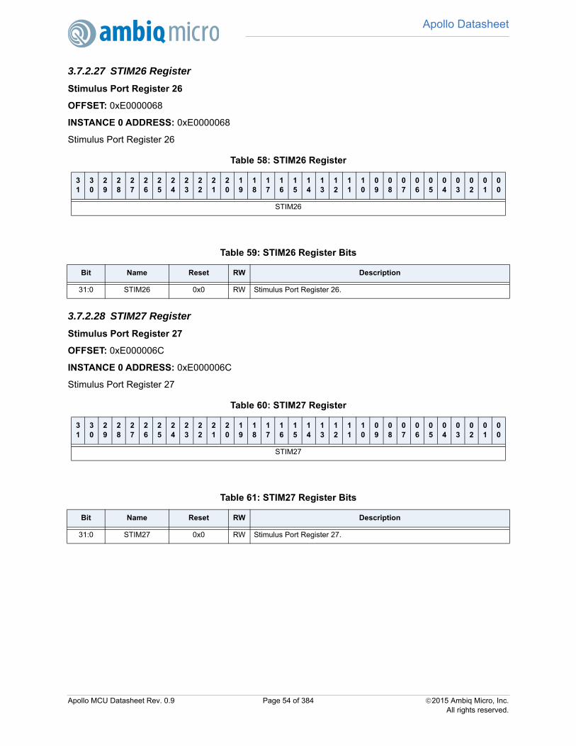
Apollo Datasheet
87
3.7.2.27 STIM26 RegisterStimulus Port Register 26
OFFSET: 0xE0000068
INSTANCE 0 ADDRESS: 0xE0000068
Stimulus Port Register 26
3.7.2.28 STIM27 Register
Stimulus Port Register 27
OFFSET: 0xE000006C
INSTANCE 0 ADDRESS: 0xE000006C
Stimulus Port Register 27
Table 58: STIM26 Register
31
30
29
28
27
26
25
24
23
22
21
20
19
18
17
16
15
14
13
12
11
10
09
08
07
06
05
04
03
02
01
00
STIM26
Table 59: STIM26 Register Bits
Bit Name Reset RW Description
31:0 STIM26 0x0 RW Stimulus Port Register 26.
Table 60: STIM27 Register
31
30
29
28
27
26
25
24
23
22
21
20
19
18
17
16
15
14
13
12
11
10
09
08
07
06
05
04
03
02
01
00
STIM27
Table 61: STIM27 Register Bits
Bit Name Reset RW Description
31:0 STIM27 0x0 RW Stimulus Port Register 27.
Apollo MCU Datasheet Rev. 0.9 Page 54 of 384 2015 Ambiq Micro, Inc.All rights reserved.

Apollo Datasheet
87
3.7.2.29 STIM28 RegisterStimulus Port Register 28
OFFSET: 0xE0000070
INSTANCE 0 ADDRESS: 0xE0000070
Stimulus Port Register 28
3.7.2.30 STIM29 Register
Stimulus Port Register 29
OFFSET: 0xE0000074
INSTANCE 0 ADDRESS: 0xE0000074
Stimulus Port Register 29
Table 62: STIM28 Register
31
30
29
28
27
26
25
24
23
22
21
20
19
18
17
16
15
14
13
12
11
10
09
08
07
06
05
04
03
02
01
00
STIM28
Table 63: STIM28 Register Bits
Bit Name Reset RW Description
31:0 STIM28 0x0 RW Stimulus Port Register 28.
Table 64: STIM29 Register
31
30
29
28
27
26
25
24
23
22
21
20
19
18
17
16
15
14
13
12
11
10
09
08
07
06
05
04
03
02
01
00
STIM29
Table 65: STIM29 Register Bits
Bit Name Reset RW Description
31:0 STIM29 0x0 RW Stimulus Port Register 29.
Apollo MCU Datasheet Rev. 0.9 Page 55 of 384 2015 Ambiq Micro, Inc.All rights reserved.

Apollo Datasheet
87
3.7.2.31 STIM30 RegisterStimulus Port Register 30
OFFSET: 0xE0000078
INSTANCE 0 ADDRESS: 0xE0000078
Stimulus Port Register 30
3.7.2.32 STIM31 Register
Stimulus Port Register 31
OFFSET: 0xE000007C
INSTANCE 0 ADDRESS: 0xE000007C
Stimulus Port Register 31
Table 66: STIM30 Register
31
30
29
28
27
26
25
24
23
22
21
20
19
18
17
16
15
14
13
12
11
10
09
08
07
06
05
04
03
02
01
00
STIM30
Table 67: STIM30 Register Bits
Bit Name Reset RW Description
31:0 STIM30 0x0 RW Stimulus Port Register 30.
Table 68: STIM31 Register
31
30
29
28
27
26
25
24
23
22
21
20
19
18
17
16
15
14
13
12
11
10
09
08
07
06
05
04
03
02
01
00
STIM31
Table 69: STIM31 Register Bits
Bit Name Reset RW Description
31:0 STIM31 0x0 RW Stimulus Port Register 31.
Apollo MCU Datasheet Rev. 0.9 Page 56 of 384 2015 Ambiq Micro, Inc.All rights reserved.

Apollo Datasheet
87
3.7.2.33 TER RegisterTrace Enable Register.
OFFSET: 0xE0000E00
INSTANCE 0 ADDRESS: 0xE0000E00
Trace Enable Register
3.7.2.34 TPR Register
Trace Privilege Register.
OFFSET: 0xE0000E40
INSTANCE 0 ADDRESS: 0xE0000E40
Trace Privilege Register
Table 70: TER Register
31
30
29
28
27
26
25
24
23
22
21
20
19
18
17
16
15
14
13
12
11
10
09
08
07
06
05
04
03
02
01
00
STIMENA
Table 71: TER Register Bits
Bit Name Reset RW Description
31:0 STIMENA 0x0 RWBit mask to enable tracing on ITM stimulus ports. One bit per stimulus port.
Table 72: TPR Register
31
30
29
28
27
26
25
24
23
22
21
20
19
18
17
16
15
14
13
12
11
10
09
08
07
06
05
04
03
02
01
00
RSVDP
RIV
MA
SK
Table 73: TPR Register Bits
Bit Name Reset RW Description
31:4 RSVD 0x0 RO RESERVED.
3:0 PRIVMASK 0x0 RWBit mask to enable tracing on ITM stimulus ports. bit[0] = stimulus ports[7:0],bit[1] = stimulus ports[15:8], bit[2] = stimulus ports[23:16], bit[3] = stimulusports[31:24].
Apollo MCU Datasheet Rev. 0.9 Page 57 of 384 2015 Ambiq Micro, Inc.All rights reserved.
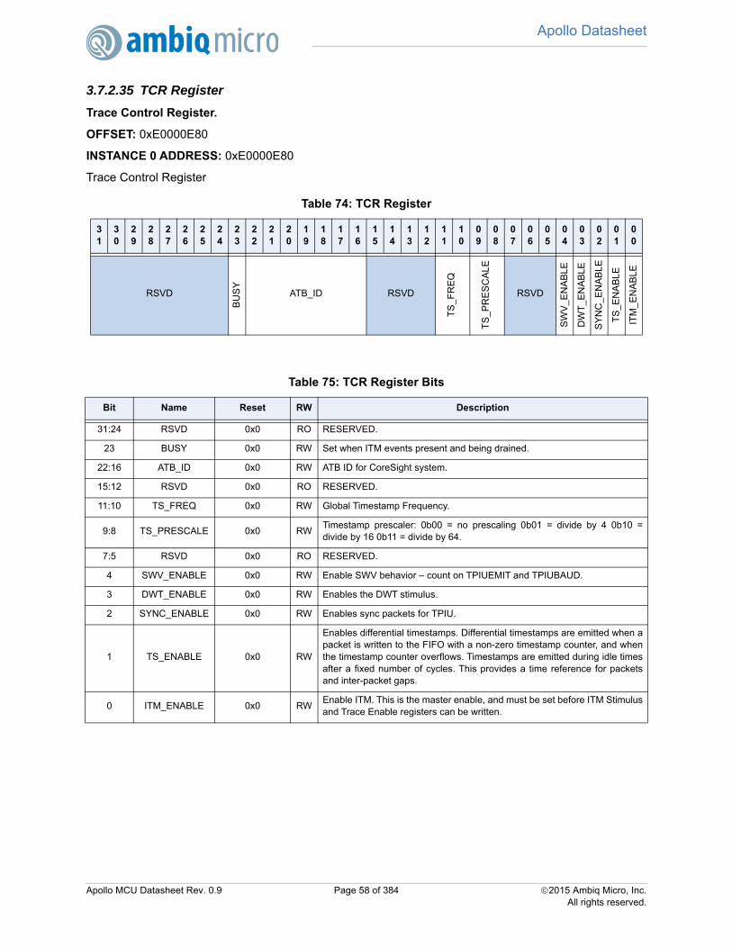
Apollo Datasheet
87
3.7.2.35 TCR RegisterTrace Control Register.
OFFSET: 0xE0000E80
INSTANCE 0 ADDRESS: 0xE0000E80
Trace Control Register
Table 74: TCR Register
31
30
29
28
27
26
25
24
23
22
21
20
19
18
17
16
15
14
13
12
11
10
09
08
07
06
05
04
03
02
01
00
RSVD
BU
SY
ATB_ID RSVD
TS
_FR
EQ
TS
_PR
ES
CA
LE
RSVD
SW
V_E
NA
BLE
DW
T_E
NA
BL
E
SY
NC
_EN
AB
LE
TS
_EN
AB
LE
ITM
_EN
AB
LE
Table 75: TCR Register Bits
Bit Name Reset RW Description
31:24 RSVD 0x0 RO RESERVED.
23 BUSY 0x0 RW Set when ITM events present and being drained.
22:16 ATB_ID 0x0 RW ATB ID for CoreSight system.
15:12 RSVD 0x0 RO RESERVED.
11:10 TS_FREQ 0x0 RW Global Timestamp Frequency.
9:8 TS_PRESCALE 0x0 RWTimestamp prescaler: 0b00 = no prescaling 0b01 = divide by 4 0b10 =divide by 16 0b11 = divide by 64.
7:5 RSVD 0x0 RO RESERVED.
4 SWV_ENABLE 0x0 RW Enable SWV behavior – count on TPIUEMIT and TPIUBAUD.
3 DWT_ENABLE 0x0 RW Enables the DWT stimulus.
2 SYNC_ENABLE 0x0 RW Enables sync packets for TPIU.
1 TS_ENABLE 0x0 RW
Enables differential timestamps. Differential timestamps are emitted when apacket is written to the FIFO with a non-zero timestamp counter, and whenthe timestamp counter overflows. Timestamps are emitted during idle timesafter a fixed number of cycles. This provides a time reference for packetsand inter-packet gaps.
0 ITM_ENABLE 0x0 RWEnable ITM. This is the master enable, and must be set before ITM Stimulusand Trace Enable registers can be written.
Apollo MCU Datasheet Rev. 0.9 Page 58 of 384 2015 Ambiq Micro, Inc.All rights reserved.

Apollo Datasheet
87
3.7.2.36 LOCKAREG RegisterLock Access Register
OFFSET: 0xE0000FB0
INSTANCE 0 ADDRESS: 0xE0000FB0
Lock Access Register
3.7.2.37 LOCKSREG Register
Lock Status Register
OFFSET: 0xE0000FB4
INSTANCE 0 ADDRESS: 0xE0000FB4
Lock Status Register
Table 76: LOCKAREG Register
31
30
29
28
27
26
25
24
23
22
21
20
19
18
17
16
15
14
13
12
11
10
09
08
07
06
05
04
03
02
01
00
LOCKAREG
Table 77: LOCKAREG Register Bits
Bit Name Reset RW Description
31:0 LOCKAREG 0x0 RWKey register value.
Key = 0xC5ACCE55 - Key
Table 78: LOCKSREG Register
31
30
29
28
27
26
25
24
23
22
21
20
19
18
17
16
15
14
13
12
11
10
09
08
07
06
05
04
03
02
01
00
RSVD
BY
TE
AC
C
AC
CE
SS
PR
ES
EN
T
Table 79: LOCKSREG Register Bits
Bit Name Reset RW Description
31:3 RSVD 0x0 RO RESERVED.
2 BYTEACC 0x0 RO You cannot implement 8-bit lock accesses.
1 ACCESS 0x0 ROWrite access to component is blocked. All writes are ignored, reads are per-mitted.
0 PRESENT 0x1 RO Indicates that a lock mechanism exists for this component.
Apollo MCU Datasheet Rev. 0.9 Page 59 of 384 2015 Ambiq Micro, Inc.All rights reserved.

Apollo Datasheet
87
3.7.2.38 PID4 RegisterPeripheral Identification Register 4
OFFSET: 0xE0000FD0
INSTANCE 0 ADDRESS: 0xE0000FD0
Peripheral Identification Register 4
3.7.2.39 PID5 Register
Peripheral Identification Register 5
OFFSET: 0xE0000FD4
INSTANCE 0 ADDRESS: 0xE0000FD4
Peripheral Identification Register 5
Table 80: PID4 Register
31
30
29
28
27
26
25
24
23
22
21
20
19
18
17
16
15
14
13
12
11
10
09
08
07
06
05
04
03
02
01
00
PID4
Table 81: PID4 Register Bits
Bit Name Reset RW Description
31:0 PID4 0x4 R0 Peripheral Identification 4.
Table 82: PID5 Register
31
30
29
28
27
26
25
24
23
22
21
20
19
18
17
16
15
14
13
12
11
10
09
08
07
06
05
04
03
02
01
00
PID5
Table 83: PID5 Register Bits
Bit Name Reset RW Description
31:0 PID5 0x0 R0 Peripheral Identification 5.
Apollo MCU Datasheet Rev. 0.9 Page 60 of 384 2015 Ambiq Micro, Inc.All rights reserved.

Apollo Datasheet
87
3.7.2.40 PID6 RegisterPeripheral Identification Register 6
OFFSET: 0xE0000FD8
INSTANCE 0 ADDRESS: 0xE0000FD8
Peripheral Identification Register 6
3.7.2.41 PID7 Register
Peripheral Identification Register 7
OFFSET: 0xE0000FDC
INSTANCE 0 ADDRESS: 0xE0000FDC
Peripheral Identification Register 7
Table 84: PID6 Register
31
30
29
28
27
26
25
24
23
22
21
20
19
18
17
16
15
14
13
12
11
10
09
08
07
06
05
04
03
02
01
00
PID6
Table 85: PID6 Register Bits
Bit Name Reset RW Description
31:0 PID6 0x0 R0 Peripheral Identification 6.
Table 86: PID7 Register
31
30
29
28
27
26
25
24
23
22
21
20
19
18
17
16
15
14
13
12
11
10
09
08
07
06
05
04
03
02
01
00
PID7
Table 87: PID7 Register Bits
Bit Name Reset RW Description
31:0 PID7 0x0 R0 Peripheral Identification 7.
Apollo MCU Datasheet Rev. 0.9 Page 61 of 384 2015 Ambiq Micro, Inc.All rights reserved.

Apollo Datasheet
87
3.7.2.42 PID0 RegisterPeripheral Identification Register 0
OFFSET: 0xE0000FE0
INSTANCE 0 ADDRESS: 0xE0000FE0
Peripheral Identification Register 0
3.7.2.43 PID1 Register
Peripheral Identification Register 1
OFFSET: 0xE0000FE4
INSTANCE 0 ADDRESS: 0xE0000FE4
Peripheral Identification Register 1
Table 88: PID0 Register
31
30
29
28
27
26
25
24
23
22
21
20
19
18
17
16
15
14
13
12
11
10
09
08
07
06
05
04
03
02
01
00
PID0
Table 89: PID0 Register Bits
Bit Name Reset RW Description
31:0 PID0 0x1 R0 Peripheral Identification 0.
Table 90: PID1 Register
31
30
29
28
27
26
25
24
23
22
21
20
19
18
17
16
15
14
13
12
11
10
09
08
07
06
05
04
03
02
01
00
PID1
Table 91: PID1 Register Bits
Bit Name Reset RW Description
31:0 PID1 0xb0 R0 Peripheral Identification 1.
Apollo MCU Datasheet Rev. 0.9 Page 62 of 384 2015 Ambiq Micro, Inc.All rights reserved.

Apollo Datasheet
87
3.7.2.44 PID2 RegisterPeripheral Identification Register 2
OFFSET: 0xE0000FE8
INSTANCE 0 ADDRESS: 0xE0000FE8
Peripheral Identification Register 2
3.7.2.45 PID3 Register
Peripheral Identification Register 3
OFFSET: 0xE0000FEC
INSTANCE 0 ADDRESS: 0xE0000FEC
Peripheral Identification Register 3
Table 92: PID2 Register
31
30
29
28
27
26
25
24
23
22
21
20
19
18
17
16
15
14
13
12
11
10
09
08
07
06
05
04
03
02
01
00
PID2
Table 93: PID2 Register Bits
Bit Name Reset RW Description
31:0 PID2 0x3b R0 Peripheral Identification 2.
Table 94: PID3 Register
31
30
29
28
27
26
25
24
23
22
21
20
19
18
17
16
15
14
13
12
11
10
09
08
07
06
05
04
03
02
01
00
PID3
Table 95: PID3 Register Bits
Bit Name Reset RW Description
31:0 PID3 0x0 R0 Peripheral Identification 3.
Apollo MCU Datasheet Rev. 0.9 Page 63 of 384 2015 Ambiq Micro, Inc.All rights reserved.

Apollo Datasheet
87
3.7.2.46 CID0 RegisterComponent Identification Register 1
OFFSET: 0xE0000FF0
INSTANCE 0 ADDRESS: 0xE0000FF0
Component Identification Register 1
3.7.2.47 CID1 Register
Component Identification Register 1
OFFSET: 0xE0000FF4
INSTANCE 0 ADDRESS: 0xE0000FF4
Component Identification Register 1
Table 96: CID0 Register
31
30
29
28
27
26
25
24
23
22
21
20
19
18
17
16
15
14
13
12
11
10
09
08
07
06
05
04
03
02
01
00
CID0
Table 97: CID0 Register Bits
Bit Name Reset RW Description
31:0 CID0 0xd R0 Component Identification 1.
Table 98: CID1 Register
31
30
29
28
27
26
25
24
23
22
21
20
19
18
17
16
15
14
13
12
11
10
09
08
07
06
05
04
03
02
01
00
CID1
Table 99: CID1 Register Bits
Bit Name Reset RW Description
31:0 CID1 0xe0 R0 Component Identification 1.
Apollo MCU Datasheet Rev. 0.9 Page 64 of 384 2015 Ambiq Micro, Inc.All rights reserved.

Apollo Datasheet
87
3.7.2.48 CID2 RegisterComponent Identification Register 2
OFFSET: 0xE0000FF8
INSTANCE 0 ADDRESS: 0xE0000FF8
Component Identification Register 2
3.7.2.49 CID3 Register
Component Identification Register 3
OFFSET: 0xE0000FFC
INSTANCE 0 ADDRESS: 0xE0000FFC
Component Identification Register 3
Table 100: CID2 Register
31
30
29
28
27
26
25
24
23
22
21
20
19
18
17
16
15
14
13
12
11
10
09
08
07
06
05
04
03
02
01
00
CID2
Table 101: CID2 Register Bits
Bit Name Reset RW Description
31:0 CID2 0x5 R0 Component Identification 2.
Table 102: CID3 Register
31
30
29
28
27
26
25
24
23
22
21
20
19
18
17
16
15
14
13
12
11
10
09
08
07
06
05
04
03
02
01
00
CID3
Table 103: CID3 Register Bits
Bit Name Reset RW Description
31:0 CID3 0xb1 R0 Component Identification 3.
Apollo MCU Datasheet Rev. 0.9 Page 65 of 384 2015 Ambiq Micro, Inc.All rights reserved.

Apollo Datasheet
87
3.8 MCUCTRL RegistersMCU Miscellaneous Control LogicINSTANCE 0 BASE ADDRESS:0x40020000
3.8.1 Register Memory Map
Table 104: MCUCTRL Register Map
Address(s) Register Name Description
0x40020000 CHIP_INFO Chip Information Register
0x40020004 CHIPID0 Unique Chip ID 0
0x40020008 CHIPID1 Unique Chip ID 1
0x4002000C CHIPREV Chip Revision
0x40020010 SUPPLYSRCMemory and Core Voltage Supply Source SelectRegister
0x40020014 SUPPLYSTATUSMemory and Core Voltage Supply Source StatusRegister
0x400200FC BANDGAPEN Band Gap Enable
0x40020140 SRAMPWDINSLEEPPowerdown an SRAM Bank in Deep Sleepmode
0x40020144 SRAMPWRDIS Disables individual banks of the SRAM array
0x40020148 FLASHPWRDIS Disables individual banks of the Flash array
0x400201C0 ICODEFAULTADDRICODE bus address which was present when abus fault occurred.
0x400201C4 DCODEFAULTADDRDCODE bus address which was present when abus fault occurred.
0x400201C8 SYSFAULTADDRSystem bus address which was present when abus fault occurred.
0x400201CC FAULTSTATUSReflects the status of the bus decoders' faultdetection. Any write to this register will clear allof the status bits within the register.
0x400201D0 FAULTCAPTUREEN Enable the fault capture registers
0x40020250 TPIUCTRLTPIU Control Register. Determines the clockenable and frequency for the M4's TPIU inter-face.
Apollo MCU Datasheet Rev. 0.9 Page 66 of 384 2015 Ambiq Micro, Inc.All rights reserved.

Apollo Datasheet
87
3.8.2 MCUCTRL Registers3.8.2.1 CHIP_INFO Register
Chip Information Register
OFFSET: 0x00000000
INSTANCE 0 ADDRESS: 0x40020000
Chip Information Register
Table 105: CHIP_INFO Register
31
30
29
28
27
26
25
24
23
22
21
20
19
18
17
16
15
14
13
12
11
10
09
08
07
06
05
04
03
02
01
00
CLASS FLASH RAM
MA
JOR
RE
V
MIN
OR
RE
V
PKG PINS
TE
MP
QU
AL
Table 106: CHIP_INFO Register Bits
Bit Name Reset RW Description
31:24 CLASS 0x1 RODevice class.
APOLLO = 0x1 - APOLLO
23:20 FLASH 0x4 RO
Device flash size.
256K = 0x3 - 256K of available flash.512K = 0x4 - 512K of available flash.
19:16 RAM 0x1 RO
Device RAM size.
32K = 0x0 - 32K of available SRAM.64K = 0x1 - 64K of available SRAM.
15:12 MAJORREV 0x1 ROMajor device revision number.
11:8 MINORREV 0x1 ROMinor device revision number.
7:6 PKG 0x1 RO
Device package type.
BGA = 0x2 - Ball grid array.CSP = 0x3 - Chip-scale package.
5:3 PINS 0x1 RO
Number of pins.
41PINS = 0x1 - 41 package pins total.64PINS = 0x1 - 64 package pins total.
2:1 TEMP 0x1 RODevice temperature range.
COMMERCIAL = 0x0 - Commercial temperature range.
Apollo MCU Datasheet Rev. 0.9 Page 67 of 384 2015 Ambiq Micro, Inc.All rights reserved.

Apollo Datasheet
87
3.8.2.2 CHIPID0 Register
Unique Chip ID 0
OFFSET: 0x00000004
INSTANCE 0 ADDRESS: 0x40020004
Unique Chip ID 0
3.8.2.3 CHIPID1 Register
Unique Chip ID 1
OFFSET: 0x00000008
INSTANCE 0 ADDRESS: 0x40020008
Unique Chip ID 1
0 QUAL 0x1 RO
Device qualified.
PROTOTYPE = 0x0 - Prototype device.QUALIFIED = 0x1 - Fully qualified device.
Table 107: CHIPID0 Register
31
30
29
28
27
26
25
24
23
22
21
20
19
18
17
16
15
14
13
12
11
10
09
08
07
06
05
04
03
02
01
00
VALUE
Table 108: CHIPID0 Register Bits
Bit Name Reset RW Description
31:0 VALUE 0x0 ROUnique chip ID 0.
APOLLO = 0x0 - Apollo CHIPID0.
Table 109: CHIPID1 Register
31
30
29
28
27
26
25
24
23
22
21
20
19
18
17
16
15
14
13
12
11
10
09
08
07
06
05
04
03
02
01
00
VALUE
Table 106: CHIP_INFO Register Bits
Bit Name Reset RW Description
Apollo MCU Datasheet Rev. 0.9 Page 68 of 384 2015 Ambiq Micro, Inc.All rights reserved.

Apollo Datasheet
87
3.8.2.4 CHIPREV Register
Chip Revision
OFFSET: 0x0000000C
INSTANCE 0 ADDRESS: 0x4002000C
Chip Revision
3.8.2.5 SUPPLYSRC Register
Memory and Core Voltage Supply Source Select Register
OFFSET: 0x00000010
INSTANCE 0 ADDRESS: 0x40020010
Memory and Core Voltage Supply Source Select Register
Table 110: CHIPID1 Register Bits
Bit Name Reset RW Description
31:0 VALUE 0x0 ROUnique chip ID 1.
APOLLO = 0x0 - Apollo CHIPID1.
Table 111: CHIPREV Register
31
30
29
28
27
26
25
24
23
22
21
20
19
18
17
16
15
14
13
12
11
10
09
08
07
06
05
04
03
02
01
00
RSVD
Table 112: CHIPREV Register Bits
Bit Name Reset RW Description
31:8 RSVD 0x0 RORESERVED.
Table 113: SUPPLYSRC Register
31
30
29
28
27
26
25
24
23
22
21
20
19
18
17
16
15
14
13
12
11
10
09
08
07
06
05
04
03
02
01
00
RSVD
CO
RE
BU
CK
EN
ME
MB
UC
KE
N
Apollo MCU Datasheet Rev. 0.9 Page 69 of 384 2015 Ambiq Micro, Inc.All rights reserved.

Apollo Datasheet
87
3.8.2.6 SUPPLYSTATUS Register
Memory and Core Voltage Supply Source Status Register
OFFSET: 0x00000014
INSTANCE 0 ADDRESS: 0x40020014
Memory and Core Voltage Supply Source Status Register
Table 114: SUPPLYSRC Register Bits
Bit Name Reset RW Description
31:2 RSVD 0x0 RORESERVED.
1 COREBUCKEN 0x0 RW
Enables and Selects the Core Buck as the supply for the low-voltage powerdomain.
EN = 0x1 - Enable the Core Buck for the low-voltage power domain.
0 MEMBUCKEN 0x0 RW
Enables and select the Memory Buck as the supply for the Flash and SRAMpower domain.
EN = 0x1 - Enable the Memory Buck as the supply for flash and SRAM.
Table 115: SUPPLYSTATUS Register
31
30
29
28
27
26
25
24
23
22
21
20
19
18
17
16
15
14
13
12
11
10
09
08
07
06
05
04
03
02
01
00
RSVD
CO
RE
BU
CK
ON
ME
MB
UC
KO
NTable 116: SUPPLYSTATUS Register Bits
Bit Name Reset RW Description
31:2 RSVD 0x0 RORESERVED.
1 COREBUCKON 0x0 RO
Indicates whether the Core low-voltage domain is supplied from the LDO orthe Buck.
LDO = 0x0 - Indicates the the LDO is supplying the Core low-voltage.BUCK = 0x1 - Indicates the the Buck is supplying the Core low-voltage.
0 MEMBUCKON 0x0 RO
Indicate whether the Memory power domain is supplied from the LDO or theBuck.
LDO = 0x0 - Indicates the LDO is supplying the memory power domain.BUCK = 0x1 - Indicates the Buck is supplying the memory power domain.
Apollo MCU Datasheet Rev. 0.9 Page 70 of 384 2015 Ambiq Micro, Inc.All rights reserved.

Apollo Datasheet
87
3.8.2.7 BANDGAPEN RegisterBand Gap Enable
OFFSET: 0x000000FC
INSTANCE 0 ADDRESS: 0x400200FC
Band Gap Enable
3.8.2.8 SRAMPWDINSLEEP Register
Powerdown an SRAM Bank in Deep Sleep mode
OFFSET: 0x00000140
INSTANCE 0 ADDRESS: 0x40020140
Powerdown an SRAM Bank in Deep Sleep mode
Table 117: BANDGAPEN Register
31
30
29
28
27
26
25
24
23
22
21
20
19
18
17
16
15
14
13
12
11
10
09
08
07
06
05
04
03
02
01
00
RSVD
BG
PE
N
Table 118: BANDGAPEN Register Bits
Bit Name Reset RW Description
31:1 RSVD 0x0 RORESERVED.
0 BGPEN 0x0 RW
Bandgap Enable
DIS = 0x0 - Bandgap disable.EN = 0x1 - Bandgap enable.
Table 119: SRAMPWDINSLEEP Register
31
30
29
28
27
26
25
24
23
22
21
20
19
18
17
16
15
14
13
12
11
10
09
08
07
06
05
04
03
02
01
00
RSVD
BA
NK
7
BA
NK
6
BA
NK
5
BA
NK
4
BA
NK
3
BA
NK
2
BA
NK
1
BA
NK
0
Apollo MCU Datasheet Rev. 0.9 Page 71 of 384 2015 Ambiq Micro, Inc.All rights reserved.

Apollo Datasheet
87
Table 120: SRAMPWDINSLEEP Register Bits
Bit Name Reset RW Description
31:8 RSVD 0x0 RORESERVED.
7 BANK7 0x0 RW
Force SRAM Bank 7 to powerdown in deep sleep mode, causing the con-tents of the bank to be lost.
NORMAL = 0x0 - SRAM Bank 7 normal operation.PWRDN_IN_DEEPSLEEP = 0x1 - SRAM Bank 7 deep sleep.
6 BANK6 0x0 RW
Force SRAM Bank 6 to powerdown in deep sleep mode, causing the con-tents of the bank to be lost.
NORMAL = 0x0 - SRAM Bank 6 normal operation.PWRDN_IN_DEEPSLEEP = 0x1 - SRAM Bank 6 deep sleep.
5 BANK5 0x0 RW
Force SRAM Bank 5 to powerdown in deep sleep mode, causing the con-tents of the bank to be lost.
NORMAL = 0x0 - SRAM Bank 5 normal operation.PWRDN_IN_DEEPSLEEP = 0x1 - SRAM Bank 5 deep sleep.
4 BANK4 0x0 RW
Force SRAM Bank 4 to powerdown in deep sleep mode, causing the con-tents of the bank to be lost.
NORMAL = 0x0 - SRAM Bank 4 normal operation.PWRDN_IN_DEEPSLEEP = 0x1 - SRAM Bank 4 deep sleep.
3 BANK3 0x0 RW
Force SRAM Bank 3 to powerdown in deep sleep mode, causing the con-tents of the bank to be lost.
NORMAL = 0x0 - SRAM Bank 3 normal operation.PWRDN_IN_DEEPSLEEP = 0x1 - SRAM Bank 3 deep sleep.
2 BANK2 0x0 RW
Force SRAM Bank 2 to powerdown in deep sleep mode, causing the con-tents of the bank to be lost.
NORMAL = 0x0 - SRAM Bank 2 normal operation.PWRDN_IN_DEEPSLEEP = 0x1 - SRAM Bank 2 deep sleep.
1 BANK1 0x0 RW
Force SRAM Bank 1 to powerdown in deep sleep mode, causing the con-tents of the bank to be lost.
NORMAL = 0x0 - SRAM Bank 1 normal operation.PWRDN_IN_DEEPSLEEP = 0x1 - SRAM Bank 1 deep sleep.
0 BANK0 0x0 RW
Force SRAM Bank 0 to powerdown in deep sleep mode, causing the con-tents of the bank to be lost.
NORMAL = 0x0 - SRAM Bank 0 normal operation.PWRDN_IN_DEEPSLEEP = 0x1 - SRAM Bank 0 deep sleep.
Apollo MCU Datasheet Rev. 0.9 Page 72 of 384 2015 Ambiq Micro, Inc.All rights reserved.

Apollo Datasheet
87
3.8.2.9 SRAMPWRDIS RegisterDisables individual banks of the SRAM array
OFFSET: 0x00000144
INSTANCE 0 ADDRESS: 0x40020144
Disables individual banks of the SRAM array
Table 121: SRAMPWRDIS Register
31
30
29
28
27
26
25
24
23
22
21
20
19
18
17
16
15
14
13
12
11
10
09
08
07
06
05
04
03
02
01
00
RSVD
BA
NK
7
BA
NK
6
BA
NK
5
BA
NK
4
BA
NK
3
BA
NK
2
BA
NK
1
BA
NK
0
Table 122: SRAMPWRDIS Register Bits
Bit Name Reset RW Description
31:8 RSVD 0x0 RORESERVED.
7 BANK7 0x0 RW
Remove power from SRAM Bank 7 which will cause an access to itsaddress space to generate a Hard Fault.
DIS = 0x1 - Disable SRAM Bank 7.
6 BANK6 0x0 RW
Remove power from SRAM Bank 6 which will cause an access to itsaddress space to generate a Hard Fault.
DIS = 0x1 - Disable SRAM Bank 6.
5 BANK5 0x0 RW
Remove power from SRAM Bank 5 which will cause an access to itsaddress space to generate a Hard Fault.
DIS = 0x1 - Disable SRAM Bank 5.
4 BANK4 0x0 RW
Remove power from SRAM Bank 4 which will cause an access to itsaddress space to generate a Hard Fault.
DIS = 0x1 - Disable SRAM Bank 4.
3 BANK3 0x0 RW
Remove power from SRAM Bank 3 which will cause an access to itsaddress space to generate a Hard Fault.
DIS = 0x1 - Disable SRAM Bank 3.
2 BANK2 0x0 RW
Remove power from SRAM Bank 2 which will cause an access to itsaddress space to generate a Hard Fault.
DIS = 0x1 - Disable SRAM Bank 2.
1 BANK1 0x0 RW
Remove power from SRAM Bank 1 which will cause an access to itsaddress space to generate a Hard Fault.
DIS = 0x1 - Disable SRAM Bank 1.
Apollo MCU Datasheet Rev. 0.9 Page 73 of 384 2015 Ambiq Micro, Inc.All rights reserved.

Apollo Datasheet
87
3.8.2.10 FLASHPWRDIS Register
Disables individual banks of the Flash array
OFFSET: 0x00000148
INSTANCE 0 ADDRESS: 0x40020148
Disables individual banks of the Flash array
0 BANK0 0x0 RW
Remove power from SRAM Bank 0 which will cause an access to itsaddress space to generate a Hard Fault.
DIS = 0x1 - Disable SRAM Bank 0.
Table 123: FLASHPWRDIS Register
31
30
29
28
27
26
25
24
23
22
21
20
19
18
17
16
15
14
13
12
11
10
09
08
07
06
05
04
03
02
01
00
RSVD
BA
NK
1
BA
NK
0
Table 124: FLASHPWRDIS Register Bits
Bit Name Reset RW Description
31:2 RSVD 0x0 RORESERVED.
1 BANK1 0x0 RW
Remove power from Flash Bank 1 which will cause an access to its addressspace to generate a Hard Fault.
DIS = 0x1 - Disable Flash instance 1.
0 BANK0 0x0 RW
Remove power from Flash Bank 0 which will cause an access to its addressspace to generate a Hard Fault.
DIS = 0x1 - Disable Flash instance 0.
Table 122: SRAMPWRDIS Register Bits
Bit Name Reset RW Description
Apollo MCU Datasheet Rev. 0.9 Page 74 of 384 2015 Ambiq Micro, Inc.All rights reserved.

Apollo Datasheet
87
3.8.2.11 ICODEFAULTADDR RegisterICODE bus address which was present when a bus fault occurred.
OFFSET: 0x000001C0
INSTANCE 0 ADDRESS: 0x400201C0
ICODE bus address which was present when a bus fault occurred.
3.8.2.12 DCODEFAULTADDR Register
DCODE bus address which was present when a bus fault occurred.
OFFSET: 0x000001C4
INSTANCE 0 ADDRESS: 0x400201C4
DCODE bus address which was present when a bus fault occurred.
Table 125: ICODEFAULTADDR Register
31
30
29
28
27
26
25
24
23
22
21
20
19
18
17
16
15
14
13
12
11
10
09
08
07
06
05
04
03
02
01
00
ADDR
Table 126: ICODEFAULTADDR Register Bits
Bit Name Reset RW Description
31:0 ADDR 0x0 RO
The ICODE bus address observed when a Bus Fault occurred. Once anaddress is captured in this field, it is held until the corresponding FaultObserved bit is cleared in the FAULTSTATUS register.
Table 127: DCODEFAULTADDR Register
31
30
29
28
27
26
25
24
23
22
21
20
19
18
17
16
15
14
13
12
11
10
09
08
07
06
05
04
03
02
01
00
ADDR
Table 128: DCODEFAULTADDR Register Bits
Bit Name Reset RW Description
31:0 ADDR 0x0 RO
The DCODE bus address observed when a Bus Fault occurred. Once anaddress is captured in this field, it is held until the corresponding FaultObserved bit is cleared in the FAULTSTATUS register.
Apollo MCU Datasheet Rev. 0.9 Page 75 of 384 2015 Ambiq Micro, Inc.All rights reserved.
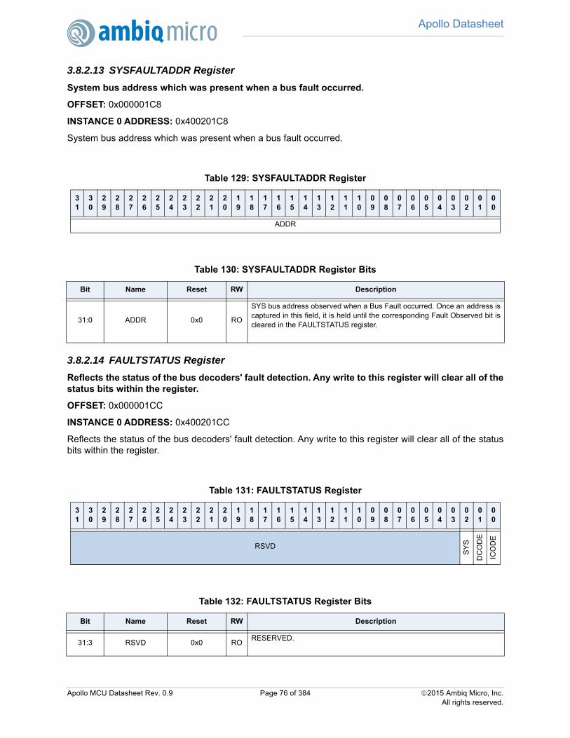
Apollo Datasheet
87
3.8.2.13 SYSFAULTADDR RegisterSystem bus address which was present when a bus fault occurred.
OFFSET: 0x000001C8
INSTANCE 0 ADDRESS: 0x400201C8
System bus address which was present when a bus fault occurred.
3.8.2.14 FAULTSTATUS Register
Reflects the status of the bus decoders' fault detection. Any write to this register will clear all of thestatus bits within the register.
OFFSET: 0x000001CC
INSTANCE 0 ADDRESS: 0x400201CC
Reflects the status of the bus decoders' fault detection. Any write to this register will clear all of the statusbits within the register.
Table 129: SYSFAULTADDR Register
31
30
29
28
27
26
25
24
23
22
21
20
19
18
17
16
15
14
13
12
11
10
09
08
07
06
05
04
03
02
01
00
ADDR
Table 130: SYSFAULTADDR Register Bits
Bit Name Reset RW Description
31:0 ADDR 0x0 RO
SYS bus address observed when a Bus Fault occurred. Once an address iscaptured in this field, it is held until the corresponding Fault Observed bit iscleared in the FAULTSTATUS register.
Table 131: FAULTSTATUS Register
31
30
29
28
27
26
25
24
23
22
21
20
19
18
17
16
15
14
13
12
11
10
09
08
07
06
05
04
03
02
01
00
RSVD
SY
S
DC
OD
E
ICO
DE
Table 132: FAULTSTATUS Register Bits
Bit Name Reset RW Description
31:3 RSVD 0x0 RORESERVED.
Apollo MCU Datasheet Rev. 0.9 Page 76 of 384 2015 Ambiq Micro, Inc.All rights reserved.

Apollo Datasheet
87
3.8.2.15 FAULTCAPTUREEN Register
Enable the fault capture registers
OFFSET: 0x000001D0
INSTANCE 0 ADDRESS: 0x400201D0
Enable the fault capture registers
2 SYS 0x0 RW
SYS Bus Decoder Fault Detected bit. When set, a fault has been detected,and the SYSFAULTADDR register will contain the bus address which gener-ated the fault.
NOFAULT = 0x0 - No bus fault has been detected.FAULT = 0x1 - Bus fault detected.
1 DCODE 0x0 RW
DCODE Bus Decoder Fault Detected bit. When set, a fault has beendetected, and the DCODEFAULTADDR register will contain the bus addresswhich generated the fault.
NOFAULT = 0x0 - No DCODE fault has been detected.FAULT = 0x1 - DCODE fault detected.
0 ICODE 0x0 RW
The ICODE Bus Decoder Fault Detected bit. When set, a fault has beendetected, and the ICODEFAULTADDR register will contain the bus addresswhich generated the fault.
NOFAULT = 0x0 - No ICODE fault has been detected.FAULT = 0x1 - ICODE fault detected.
Table 133: FAULTCAPTUREEN Register
31
30
29
28
27
26
25
24
23
22
21
20
19
18
17
16
15
14
13
12
11
10
09
08
07
06
05
04
03
02
01
00
RSVD
EN
AB
LE
Table 134: FAULTCAPTUREEN Register Bits
Bit Name Reset RW Description
31:1 RSVD 0x0 RORESERVED.
0 ENABLE 0x0 RW
Fault Capture Enable field. When set, the Fault Capture monitors areenabled and addresses which generate a hard fault are captured into theFAULTADDR registers.
DIS = 0x0 - Disable fault capture.EN = 0x1 - Enable fault capture.
Table 132: FAULTSTATUS Register Bits
Bit Name Reset RW Description
Apollo MCU Datasheet Rev. 0.9 Page 77 of 384 2015 Ambiq Micro, Inc.All rights reserved.

Apollo Datasheet
87
3.8.2.16 TPIUCTRL RegisterTPIU Control Register. Determines the clock enable and frequency for the M4's TPIU interface.
OFFSET: 0x00000250
INSTANCE 0 ADDRESS: 0x40020250
TPIU Control Register. Determines the clock enable and frequency for the M4's TPIU interface.
Table 135: TPIUCTRL Register
31
30
29
28
27
26
25
24
23
22
21
20
19
18
17
16
15
14
13
12
11
10
09
08
07
06
05
04
03
02
01
00
RSVD
CL
KS
EL
RSVD
EN
AB
LE
Table 136: TPIUCTRL Register Bits
Bit Name Reset RW Description
31:10 RSVD 0x0 RORESERVED.
9:8 CLKSEL 0x0 RW
This field selects the frequency of the ARM M4 TPIU port.
LOW_PWR = 0x0 - Low power state.0MHz = 0x0 - Low power state.6MHZ = 0x1 - Selects 6MHz frequency.3MHZ = 0x2 - Selects 3MHz frequency.1_5MHZ = 0x3 - Selects 1.5 MHz frequency.
7:1 RSVD 0x0 RORESERVED.
0 ENABLE 0x0 RW
TPIU Enable field. When set, the ARM M4 TPIU is enabled and data can bestreamed out of the MCU's SWO port using the ARM ITM and TPIU mod-ules.
DIS = 0x0 - Disable the TPIU.EN = 0x1 - Enable the TPIU.
Apollo MCU Datasheet Rev. 0.9 Page 78 of 384 2015 Ambiq Micro, Inc.All rights reserved.

Apollo Datasheet
87
4. Memory Subsystem
4.1 Flash and OTP Memory Subsystem
Figure 5. Block Diagram for Flash and OTP Subsystem
4.1.1 Features
The Apollo MCU integrates four kinds of memory as shown in Figure 5:
SRAM Flash Boot Loader ROM One Time Programmable (OTP) memory
This chapter discusses the latter three types.
Key features include:
Up to 2 Instances of 256 KB flash Memory 2048 Bytes OTP
- 1024 Bytes contain factory preset per chip trim values.- 1024 Bytes for customer use, including flash protection fields
Flash Protection specified in 16 KB Chunks- 32 OTP bits specify Write Protected Chunks- 32 OTP bits specify Read Protected Chunks - A Chunk is Execute Only if Both Corresponding Protection Bits Specified- OTP bits Specify Debugger Lock Out State- OTP bits Can Protect SRAM Contents From Debugger Inspection
256KB
Flash
Instance
256KB
Flash
Instance
8K
B S
RA
M
8K
B S
RA
M
8K
B S
RA
M
8K
B S
RA
M
8K
B S
RA
M
8K
B S
RA
M
8K
B S
RA
M
8K
B S
RA
M
AHB
FABRIC
ARM
M4F
CORE
SYS
DATA
INST
FLASH
& OTP
CONTROLB
RID
GE
APB
2K
B O
TP
Boot
Loader
ROM
Apollo MCU Datasheet Rev. 0.9 Page 79 of 384 2015 Ambiq Micro, Inc.All rights reserved.

Apollo Datasheet
87
4.1.2 Functional OverviewThe Apollo MCU Integrates up to 512 KBytes of on-board flash memory and 2048 bytes of one timeprogrammable memory. These two memories are managed by the APB flash controller for writeoperations.
During normal MCU code execution, the Flash Memory Controller translates requests from the CPU coreto the Flash Memory instance for instruction and data fetches. The Controller is designed to return data inzero wait-states and can operate up to the maximum operating frequency of the CPU core.
The Controller facilitates flash erase and programming operations. When erase or programmingoperations are active, instructions cannot be fetched for execution from the Flash memory, so the on-chipSRAM would have to be used for code execution. To facilitate the management of flash updates and OTPprogramming, a number of flash helper functions are provided in the boot loader ROM.
The boot loader ROM contains approximately 2 KB of instructions that are executed upon power up of theprocessor. Once a valid reset vector is establish at offset zero in the flash memory, the boot loadertransfers control to users application by issuing a POR type reset which causes the core to enter the resetvector in flash. This process occupies less than 100 instructions in the boot loader. The remainder of theboot loader is occupied by a set of flash helper functions.
Flash helper functions can be called directly from code executing in flash to erase or program other pagesof flash memory than the one in execution. The helper functions include a mass erase function that willerase the entire contents of a flash instance. Obviously this type of function must be called from coderunning in SRAM or there will be no caller function to return to. Finally, the helper functions includeoperations that can be invoked directly from a debugger. For these functions, a few parameters areinitialized in SRAM and a body of code is copied to SRAM. The debugger sets the PC to the flash helperfunction entry point and resumes the M4F processor from that point. This type of helper function hits a hardcoded breakpoint at the end of execution and returns to the debugger. The latter are used to initiallydownload programs into flash.
4.1.3 Directly Called Flash Helper Functions
The following flash helper functions are intended to be called directly from programs running either in flashor in SRAM. These are standard C functions that perform the standard operations on either the flash or theOTP.
4.1.3.1 Directly Called Function to Erase Main Block of Flash
Use this function to erase the entire contents of one instance (256 KB) of a flash.
/****************************************//**
* @brief entry point for erasing the MAIN block of one entire flash instance
*
* This function operates on one flash instance per call.
*
* Calling this function erases an entire flash instance (256 KB).
*
* @param value PROGRAM key
* @param flash_inst 0 or 1 selects first or second flash block
* @return 0 for success, non-zero for failure
*
*******************************************/
Apollo MCU Datasheet Rev. 0.9 Page 80 of 384 2015 Ambiq Micro, Inc.All rights reserved.

Apollo Datasheet
87
#define PROGRAM_KEY (0x12344321)int flash_mass_erase(
uint32_t value,
uint32_t flash_inst
);
4.1.3.2 Directly Called Function to Erase one Page in the Flash
One page in the flash is 2048 bytes. This function can be used to erase one page at a time.
/****************************************//**
* @brief entry point for erasing one page in the MAIN block of one flash instance
*
* This function operates on one page of the MAIN block of one flash instance per call.
*
* Calling this function erases one page in the MAIN block of one flash instance (2048 bytes).
*
* @param value PROGRAM key
* @param flash_inst 0 or 1 selects first or second flash block
* @param PageNumber offset to a page aligned target location to begin page erasing in the flash MAIN block
* @return 0 for success, non-zero for failure
*
*******************************************/
#define PROGRAM_KEY (0x12344321)
int flash_page_erase(
uint32_t value,
uint32_t flash_inst,
uint32_t PageNumber
);
4.1.3.3 Directly Called Function to Program N Words in the User Portion of the OTP
Use this function to write words in the OTP such as the protection bits or other user desired permanentinformation such as a unique ID.
/****************************************//**
* @brief entry point for programming the user portion (1024 bytes) of the 2048 byte OTP.
*
* Calling this function programs multiple words in the OTP
*
* @param value OTP program key
* @param OTP_inst always set to zero
* @param pSrc pointer to word aligned array of data to program into the OTP.
* @param Offset word offset in to the OTP (0x01 means the second 32 bit word)
* NOTE Offset == 0 --> first word in second half of OTP, 0x400 into the 2048 byte page
Apollo MCU Datasheet Rev. 0.9 Page 81 of 384 2015 Ambiq Micro, Inc.All rights reserved.

Apollo Datasheet
87
* @param NumberOfWords number of words to program* NOTE Only the upper half of the OTP can be written so 1 < NumberOfWords < 257
* @return 0 for success, non-zero for failure
*
*******************************************/
#define OTP_PROGRAM_KEY (0x87655678)
int flash_program_otp_area(
uint32_t value,
uint32_t OTP_inst,
uint32_t *pSrc,
uint32_t Offset, // 0 <= Offset < 256
uint32_t NumberOfWords // 1 < NumberOfWords < 257
);
4.1.3.4 Directly Called Function to Program N words in the Flash
Use this function to write words to an erased block of flash. NOTE: the flash does not support overwritingwords without an intervening erase operation.
/****************************************//**
* @brief Program N words of the MAIN block of one flash instance
*
* Calling this function programs N words of the MAIN block of 1 flash instance
*
* @param value PROGRAM key
* @param flash_inst 0 or 1 selects first or second flash block.
* @param pSrc pointer to word aligned data to program into the flash MAIN block.
* WARNING: pSrc can not point back in to flash itself
* @param pDst pointer to word aligned target location to begin programming in the flash MAIN block
* NOTE: we discard any bits above 256 K and below bit 2 (stays within one instance & word aligned)
* @param NumberOfWords number of 32-bit words to program
* @return 0 for success, non-zero for failure
*
*
*******************************************/
#define PROGRAM_KEY (0x12344321)
int flash_program_main(
uint32_t value,
uint32_t *pSrc,
uint32_t *pDst,
uint32_t NumberOfWords
);
Apollo MCU Datasheet Rev. 0.9 Page 82 of 384 2015 Ambiq Micro, Inc.All rights reserved.

Apollo Datasheet
87
4.1.4 Debugger Invoked Helper FunctionsThe following functions are intended to be invoked from an external debugger or debugger surrogate suchas a manufacturing gang programmer. The debugger sets up a few parameters in SRAM and copies thebinary data to be programmed in to the flash in to the SRAM behind the parameters. It then sets the PC tothe entry point for this function and resumes execution from there. When the function completes, it hits ahard coded break point instruction which passes control back to the debugger or debugger surrogate.
4.1.4.1 Program Words In The Flash From a Debugger
The debugger uses this function to copy binary data from SRAM to a target location in flash.
/****************************************//**
* @brief entry point for reading program details and data from SRAM and then programming it into MAIN
*
* Calling this function looks up programming information from offset 0x0 in SRAM
* 0x10000000 pointer in to flash
* 0x10000004 number of 32-bit words to program
* 0x10000008 PROGRAM key to pass to flash helper routine
* 0x1000000C return code debugger sets this to -1 all RCs are >= 0
* 0x10000010 first 32-bit word of data buffer to be programmed
*
* Note this routine hits a break point instruction to transfer control to a debugger surrogate in the parallel programmer.
*
* @return never returns, spins here waiting for debugger or debugger surrogate on the parallel programmer
*
*
*******************************************/
#define PROGRAM_KEY (0x12344321)
void flash_program_main_from_sram(void);
4.1.4.2 Program Words in the OTP From a Debugger
The debugger uses this function to copy binary data from SRAM to a target location in the OTP.
/****************************************//**
* @brief entry point for reading program details and data from SRAM and then programming it into the OTP
*
* Calling this function looks up programming information from offset 0x0 in SRAM
* 0x10000000 Offset in to the OTP block (user portion)
* 0 <= Offset < 256
* 256 added to offset before programming
* 0x10000004 number of 32-bit words to program
* 0x10000008 OTP program key to pass to flash helper routine
* 0x1000000C return code debugger sets this to -1 all RCs are >= 0
* 0x10000010 first 32-bit word of data buffer to be programmed
*
Apollo MCU Datasheet Rev. 0.9 Page 83 of 384 2015 Ambiq Micro, Inc.All rights reserved.

Apollo Datasheet
87
* Note this routine hits a break point instruction to transfer control to a debugger surrogate in the parallel programmer.*
* @return never returns, spins here waiting for debugger or debugger surrogate on the parallel programmer
*
*
*******************************************/
#define OTP_PROGRAM_KEY (0x87655678)
void flash_program_otp_area_from_sram(void);
4.1.4.3 Erase a Number of Contiguous Pages From a Debugger
The debugger uses this function to erase a number of contiguous pages in flash.
/****************************************//**
* @brief entry point for erasing a contiguous block of main block pages from SRAM
*
* Calling this function looks up page erase information from offset 0x0 in SRAM
* 0x10000000 instance number
* 0x10000004 number of main block pages to erase must be between 1 and 128 inclusive
* 0 < number < 129
* 0x10000008 PROGRAM key to pass to flash helper routine
* 0x1000000C return code debugger sets this to -1 all RCs are >= 0
* 0x10000010 PageNumber of the first flash page to erase. NOTE: these now *HAVE* to be sequential
* range 0 <= PageNumber <= 127
*
* Note this routine hits a break point instruction to transfer control to a debugger surrogate in the parallel programmer.
*
* @return never returns, spins here waiting for debugger or debugger surrogate on the parallel programmer
*
*
*******************************************/
void flash_erase_main_pages_from_sram(void);
Apollo MCU Datasheet Rev. 0.9 Page 84 of 384 2015 Ambiq Micro, Inc.All rights reserved.

Apollo Datasheet
87
4.1.4.4 Erase an Entire Flash Instance From a DebuggerThe debugger uses this function to an entire flash instance.
/****************************************//**
* @brief entry point for reading mass erase parameters from SRAM and then erasing the main block
*
* Calling this function looks up programming information from offset 0x0 in SRAM
* 0x10000000 pointer in to flash instance #
* 0x10000004 program key to pass to flash helper routine
* 0x10000008 return code debugger sets this to -1 all RCs are >= 0
*
* Note this routine spins when flash_mass_erase() returns and waits for the debugger surrogate in the parallelprogrammer.
*
* @return never returns, spins here waiting for debugger or debugger surrogate on the parallel programmer
*
*
*******************************************/
void flash_mass_erase_from_sram(void);
4.1.5 HAL Support for the Flash Helper Functions
The AmbiqSuite firmware Hardware Abstraction Layer (HAL) provides routines for finding and accessingall of the directly called flash helper functions. The HAL contains a function pointer table to gain access tothe flash helper functions which looks like this:
//
// Structure of function pointers to helper functions for invoking various
// flash operations.
//
typedef struct am_hal_flash_helper_struct
int (*am_hal_flash_mass_erase)(uint32_t, uint32_t);
int (*am_hal_flash_page_erase)(uint32_t, uint32_t, uint32_t);
int (*am_hal_flash_program_main)(uint32_t, uint32_t *, uint32_t *, uint32_t);
int (*am_hal_flash_program_otp)(uint32_t, uint32_t, uint32_t *, uint32_t, uint32_t);
void (*am_hal_flash_program_main_sram)(void);
void (*am_hal_flash_program_otp_sram)(void);
void (*am_hal_flash_erase_main_pages_sram)(void);
void (*am_hal_flash_mass_erase_sram)(void);
g_am_hal_flash_t;
extern g_am_hal_flash_t g_am_hal_flash;
Apollo MCU Datasheet Rev. 0.9 Page 85 of 384 2015 Ambiq Micro, Inc.All rights reserved.

Apollo Datasheet
87
It also contains constant address assignment pointers like this://
// Look-up table
//
g_am_hal_flash_t g_am_hal_flash =
// am_hal_flash_mass_erase
((int (*)(uint32_t, uint32_t)) 0x0800004d),
// am_hal_flash_page_erase
((int (*)(uint32_t, uint32_t, uint32_t)) 0x08000051),
// am_hal_flash_program_main
((int (*)(uint32_t, uint32_t *, uint32_t *, uint32_t)) 0x08000055),
// am_hal_flash_program_otp
((int (*)(uint32_t, uint32_t, uint32_t *, uint32_t, uint32_t)) 0x08000059),
// am_hal_flash_program_main_sram
((void (*)(void)) 0x0800005d),
// am_hal_flash_program_otp_sram
((void (*)(void)) 0x08000061),
// am_hal_flash_erase_main_pages_sram
((void (*)(void)) 0x08000065),
// am_hal_flash_mass_erase_sram
((void (*)(void)) 0x08000069)
;
Finally, as an example of the HAL abstraction of the flash helper functions:
//*****************************************************************************
//
//! @brief This programs up to N bytes of the Main array on one flash Instance.
//!
//! @param ui32Value - The Program key.
//! @param pui32Src - Pointer to word aligned array of data to program into
//! the flash block.
//! @param pui32Dst - Pointer to word aligned location to begin programming
//! the flash block.
//! @param ui32NumWords - The Number of words to program.
//!
//! This function will program multiple words in the FLAASH instance
//! instance 0.
//!
Apollo MCU Datasheet Rev. 0.9 Page 86 of 384 2015 Ambiq Micro, Inc.All rights reserved.

Apollo Datasheet
87
//!//! @return 0 for success, non-zero for failure.
//
//*****************************************************************************
int
am_hal_flash_program_main(uint32_t ui32Value, uint32_t *pui32Src,
uint32_t *pui32Dst, uint32_t ui32NumWords)
return g_am_hal_flash.am_hal_flash_program_main(ui32Value, pui32Src,
pui32Dst, ui32NumWords);
Apollo MCU Datasheet Rev. 0.9 Page 87 of 384 2015 Ambiq Micro, Inc.All rights reserved.

Apollo Datasheet
110
5. I2C/SPI Master Module
Figure 6. Block diagram for the I2C/SPI Master Module
5.1 Functional Overview
The Apollo MCU includes two I2C/SPI Master Modules, shown in Figure 6, each of which functions as the
Master of an I2C or SPI interface as selected by the REG_IOMSTRn_IOMCFG_IFCSEL bit (n=0 or 1). A64-byte bidirectional FIFO and a sophisticated Command mechanism allow simple initiation of I/Ooperations without requiring software interaction.
In I2C mode the I2C/SPI Master supports 7- and 10-bit addressing, multi-master arbitration, interface
frequencies from 1.2 kHz to 1.0 MHz and up to 255-byte burst operations. In SPI mode the I2C/SPI Mastersupports up to 8 slaves with automatic nCE selection, 3 and 4-wire implementation, interface frequenciesfrom 1.2 kHz to 8 MHz, all SPI polarity/phase combinations and up to 4095-byte burst operations, with bothstandard embedded address operations and raw read/write transfers.
5.2 Interface Clock Generation
The I2C/SPI Master can generate a wide range of I/O interface clocks, as shown in Figure 7. The sourceclock is a scaled version of the HFRC 24 MHz clock, selected by REG_IOMSTRn_CLKCFG_FSEL. Adivide-by-3 circuit may be selected by REG_IOMSTRn_CLKCFG_DIV3, which is particularly important increating a useful SPI frequency of 8 MHz. The output of the divide-by-3 circuit may then be divided by an8-bit value, REG_IOMSTRn_CLKCFG_TOTPER + 1, to produce the interface clock. This structure allows
I2C/SPI
Interface
(Bit SM)
To PinsIOSM
LRAM
Bus Interface
REQs
Ints
TOPSM (Counters,
Pointers)
ADDR, WDATA
RDATA
ADDR,
WDATA
RDATA
BYTESM
IOCLK
Clock
GeneratorCLKEXT
Regs
Apollo MCU Datasheet Rev. 0.9 Page 88 of 384 2015 Ambiq Micro, Inc.All rights reserved.

Apollo Datasheet
110
very precise specification of the interface frequency, and produces a minimum available interfacefrequency of 1.2 kHz. If TOTPER division is enabled by REG_IOMSTRn_CLKCFG_DIVEN, the length ofthe low period of the clock is specified by REG_IOMSTRn_CLKCFG_LOWPER + 1. Otherwise, the clockwill have a 50% duty cycle.Figure 7. I2C/SPI Master Clock Generation
5.2.1 Command Operation
In order to minimize the amount of time the CPU must be awake during I2C/SPI Master operations, the
architecture of the I2C/SPI Master is organized around processing Commands which transfer data to andfrom an internal 64-byte FIFO. For writes to the interface, software fills the FIFO and then sends a single
Command to the REG_IOMSTRn_CMD Register. The Command includes either the I2C slave address or
the SPI channel select, the desired address offset and the length of the transfer. At that point the I2C/SPIMaster executes the entire transfer, so the CPU can go to sleep. If more than 64 bytes are to betransferred, the Master will generate an interrupt when the FIFO crosses the write threshold
REG_IOMSTRn_FIFOTHR_FIFOWTHR so the CPU can wake up and refill the FIFO. The I2C/SPI Masterwill generate an interrupt when the Command is complete. In each case, the total number of bytestransferred in each operation is specified in the LENGTH field of the CMD Register.
For reads, the CMD Register is first written with the Command and the CPU can go to sleep. The Masterinitiates the read and transfers read data to the FIFO. If the FIFO crosses the read thresholdREG_IOMSTRn_FIFOTHR_FIFORTHR, an interrupt is generated so the CPU can wake up and empty theFIFO. An interrupt is also generated when the Command completes.
If the FIFO empties on a write or fills on a read, the I2C/SPI Master will simply pause the interface clockuntil the CPU has read or written a byte from the FIFO. If software initiates an incorrect operation, such asattempting to read the FIFO on a write operation or when it is empty, or write the FIFO on a read operationor when it is full, the Master will generate an IACC error interrupt. If software attempts to write theCommand Register when another Command is underway, the Master will generate an ICMD errorinterrupt.
5.2.2 FIFO
The I2C/SPI Master includes a 64-byte local RAM (LRAM) for data transfers. The LRAM functions as aFIFO. Only 32-bit word accesses are supported to the FIFO from the CPU. When a write operation isunderway, a word written to the FIFO will increment the REG_IOMSTRn_FIFOPTR_FIFOSIZ register by 4and decrement the REG_IOMSTRn_FIFOPTR_FIFOREM register by 4. Reading a byte from the FIFO viathe I/O interface decrements FIFOSIZ by 1 and increments FIFOREM by 1. When a read operation isunderway, a word read from the FIFO decrements FIFOSIZ by 4 and increments FIFOREM by 4. A byteread from the I/O interface into the FIFO increments FIFOSIZ by 1 and decrements FIFOREM by 1. If
24 MHz
768 kHz
... CLKCTR
LOWCMP
TOTCMP
CLKFF
Set
Clr
IFC_CLKFSEL
DIV3
DIV3
DIVEN
Apollo MCU Datasheet Rev. 0.9 Page 89 of 384 2015 Ambiq Micro, Inc.All rights reserved.

Apollo Datasheet
110
FIFOSIZ becomes zero during a write operation or 0x40 on a read operation and there is more data to betransferred, the clock of the I/O interface is paused until software accesses the FIFO.Two threshold registers, FIFORTHR and FIFOWTHR indicate when a THR interrupt should be generatedto signal the processor that data should be transferred.
5.2.3 I2C Interface
The I2C/SPI Master supports a flexible set of Commands to implement a variety of standard I2C
operations. The I2C interface consists of two lines: one bi-directional data line (SDA) and one clock line(SCL). Both the SDA and the SCL lines must be connected to a positive supply voltage via a pull-upresistor. By definition, a device that sends a message is called the “transmitter”, and the device thataccepts the message is called the “receiver”. The device that controls the message transfer by driving SCL
is called “master”. The devices that are controlled by the master are called “slaves”. The Apollo MCU I2CMaster is always a master device.
The following protocol has been defined:
Data transfer may be initiated only when the bus is not busy. During data transfer, the data line must remain stable whenever the clock line is high. Changes in the data line while the clock line is high will be interpreted as control signals.
A number of bus conditions have been defined (see Figure 8) and are described in the following sections.
Figure 8. Basic I2C Conditions
5.2.3.1 Bus Not Busy
Both SDA and SCL remain high.
5.2.3.2 Start Data Transfer
A change in the state of SDA from high to low, while SCL is high, defines the START condition. A STARTcondition which occurs after a previous START, but before a STOP, is called a RESTART condition, andfunctions exactly like a normal STOP followed by a normal START.
5.2.3.3 Stop Data Transfer
A change in the state of SDA from low to high, while SCL is high, defines the STOP condition.
5.2.3.4 Data Valid
After a START condition, SDA is stable for the duration of the high period of SCL. The data on SDA may bechanged during the low period of SCL. There is one clock pulse per bit of data. Each data transfer isinitiated with a START condition and terminated with a STOP condition. The number of data bytes
SDA
SCL
START SDA Stable
SDA may
change
STOP
Not Busy
Apollo MCU Datasheet Rev. 0.9 Page 90 of 384 2015 Ambiq Micro, Inc.All rights reserved.

Apollo Datasheet
110
transferred between the START and STOP conditions is not limited. The information is transmitted byte-wide and each receiver acknowledges with a ninth bit.5.2.3.5 Acknowledge
Each byte of eight bits is followed by one acknowledge (ACK) bit as shown in Figure 9. This acknowledgebit is a low level driven onto SDA by the receiver, whereas the master generates an extra acknowledgerelated SCL pulse. A slave receiver which is addressed is obliged to generate an acknowledge after thereception of each byte. Also, on a read transfer, a master receiver must generate an acknowledge after thereception of each byte that has been clocked out of the slave transmitter. The device that acknowledgesmust pull down the SDA line during the acknowledge clock pulse in such a way that the SDA line is astable low during the high period of the acknowledge related SCL pulse. A master receiver must signal anend-of-data to the slave transmitter by not generating an acknowledge (a NAK) on the last byte that hasbeen clocked out of the slave. In this case, the transmitter must leave the data line high to enable themaster to generate the STOP condition.
Figure 9. I2C Acknowledge
5.2.3.6 I2C Slave Addressing
For normal I2C reads and writes, the Command specifies the address to be sent on the interface. Both 7-bit and 10-bit addressing are supported, as selected by 10BIT in the Command. The address is specifiedin the ADDRESS field.
Figure 10 shows the operation in 7-bit mode in which the master addresses the slave with a 7-bit addressconfigured as 0xD0 in the lower 7 bits of the ADDRESS field. After the START condition, the 7-bit addressis transmitted MSB first. If this address matches the lower 7 bits of an attached slave device, the eighth bitindicates a write (RW = 0) or a read (RW = 1) operation and the slave supplies the ACK. If no slaveacknowledges the address, the transfer is terminated and a NAK error interrupt is generated.
Figure 10. I2C 7-bit Address Operation
Figure 11 shows the operation with which the master addresses the Apollo MCU with a 10-bit addressconfigured at 0x536. After the START condition, the 10-bit preamble 0b11110 is transmitted first, followedby the upper two bits of the ADDRESS field and the eighth bit indicating a write (RW = 0) or a read (RW =1) operation. If the upper two bits match the address of an attached slave device, it supplies the ACK. Thenext transfer includes the lower 8 bits of the ADDRESS field, and if these bits also match I2CADDR theslave again supplies the ACK. If no slave acknowledges either address byte, the transfer is terminated anda NAK error interrupt is generated.
SDA
SCL
START
MSB (bit 7) Bit 6 Bit 0 ACK
1 2 8 9
A1 1 0 1 0 0 0SDA
SCL
R
W
Apollo MCU Datasheet Rev. 0.9 Page 91 of 384 2015 Ambiq Micro, Inc.All rights reserved.

Apollo Datasheet
110
Figure 11. I2C 10-bit Address Operation
5.2.3.7 I2C Offset Address Transmission
If the OPER field of the CMD selects a Normal Read or Write, the I2C/SPI Master will first send an 8-bitOffset Address byte, where the offset is specified in the OFFSET field of CMD. This transfer is shown inFigure 12. The Offset Address is loaded into the Address Pointer of the slave.
Figure 12. I2C Offset Address Transmission
5.2.3.8 I2C Normal Write Operation
In a Normal write operation the I2C/SPI Master transmits to a slave receiver. The Address Operation has aRW value of 0, and the second byte contains the Offset Address, as in Figure 12. The next byte is writtento the slave register selected by the Address Pointer (which was loaded with the Offset Address) and theAddress Pointer is incremented. Subsequent transfers write bytes into successive registers until a STOPcondition is received, as shown in Figure 13.
Figure 13. I2C Normal Write Operation
5.2.3.9 I2C Normal Read Operation
If a Normal Read operation is selected in the OPER field of the Command, the I2C/SPI Master firstexecutes an Offset Address Transmission to load the Address Pointer of the slave with the desired OffsetAddress. A subsequent operation will again issue the address of the slave but with the RW bit as a 1indicating a read operation. As shown in Figure 14, this transaction begins with a RESTART condition sothat the interface will be held in a multi-master environment. After the address operation, the slavebecomes the transmitter and sends the register value from the location pointed to by the Address Pointer,and the Address Pointer is incremented. Subsequent transactions produce successive register values,
until the I2C/SPI Master receiver responds with a NAK and a STOP to complete the operation.
A1 1 1 1 0 1 0SDA
SCL
R
WA1 0 0 1 1 0 1 1
A1 1 0SDA
SCL
0 A7 6 1 0
Offset Address
0 1 0 0 5 4 3 2
Addr OffsetSDA
SCL
7 0
Byte N
AW A A 7 0
Byte N+1
A 7 0
Byte N+2
A
Apollo MCU Datasheet Rev. 0.9 Page 92 of 384 2015 Ambiq Micro, Inc.All rights reserved.

Apollo Datasheet
110
Figure 14. I2C Normal Read Operation
5.2.3.10 I2C Raw Write Operation
If a Raw Write is selected in the OPER field of the Command, the I2C/SPI Master does not execute theOffset Address Transmission, but simply begins transferring bytes as shown in Figure 15. This providessupport for slave devices which do not implement the standard offset address architecture. The OFFSETfield of Command is not used in this case.
Figure 15. I2C Raw Write Operation
5.2.3.11 I2C Raw Read Operation
If a Raw Read is selected in the OPER field of Command, the I2C/SPI Master does not execute the OffsetAddress Transmission, but simply begins transferring bytes with a read as shown in Figure 16. This isimportant for slave devices which do not support an Address Pointer architecture. For devices which doinclude an Address Pointer, multiple Raw Reads may be executed after a Normal Read to accesssubsequent registers as the Address Pointer increments, without having to execute the Offset AddressTransmission for each access.
Figure 16. I2C Raw Read Operation
5.2.3.12 Holding the Interface with CONT
In all of the previously described transactions, the I2C/SPI Master terminates the I2C operation with a
STOP sequence. In environments where there are other masters connected to the I2C interface, it may benecessary for the Apollo MCU to hold the interface between Commands to insure that another masterdoes not inadvertently access the same slave that the Apollo MCU is accessing. In order to implement this
SDA
SCL
7 0
Byte N
A A 7 0
Byte N+1
NAddr AR
RESTART
Addr OffsetAW
AddrSDA
SCL
7 0
Byte 1
AW A 7 0
Byte 2
A 7 0
Byte N
A7 0
Byte 0
A
SDA
SCL
7 0
Byte N
A 7 0
Byte N+1
NAddr AR
Apollo MCU Datasheet Rev. 0.9 Page 93 of 384 2015 Ambiq Micro, Inc.All rights reserved.

Apollo Datasheet
110
functionality, the CONT bit should be set in the CMD Register. This will cause the I2C/SPI Master to keepSDA high at the end of the transfer so that a STOP does not occur, and the next transaction begins with aRESTART instead of a START. Note that for a Normal Read the interface is held between the OffsetAddress Transmission and the actual read independent of the state of CONT, but it CONT is set the readtransaction will not terminate with a STOP.
5.2.3.13 I2C Multi-master Arbitration
The Apollo MCU I2C/SPI Master supports multi-master arbitration in I2C mode. There are two cases whichmust be handled.
The first is the case where another master initiates an I2C operation when the Apollo MCU Master is
inactive. In this case the I2C/SPI Master will detect an I2C START operation on the interface and theSTART interrupt will be asserted, which tells the software not to generate any IO operations (which will notbe executed in any case). Software then waits for the STOP interrupt, which reenables operation.
The second case is where another master initiates an operation at the same time as the Apollo MCU. Inthis case there will be a point where one master detects that it is not driving SDA low but the bus signal is
low, and that master loses the arbitration to the other master. If the Apollo MCU I2C/SPI Master detectsthat it has lost arbitration, it will assert the ARB interrupt and immediately terminate its operation. Softwaremust then wait for the STOP interrupt and re-execute the current Command.
5.2.4 SPI Operations
5.2.4.1 SPI Configuration
The I2C/SPI Master supports all combinations of the polarity (CPOL) and phase (CPHA) modes of SPIusing the REG_IOMSTRn_IOMCFG_SPOL and REG_IOMSTRn_IOMCFG_SPHA bits. It also may beconfigured in either 3-wire or 4-wire mode. In 4-wire mode, the MOSI and MISO interface signals useseparate IO pins. In 3-wire mode, MOSI and MISO are multiplexed on a single IO pin for more efficient pinutilization. The 3/4 wire configuration is selected in the mapping function of the PINCFG module.
SPI operations may transfer up to 4095 bytes in a single transfer, as the UPLNGTH field of the CMDRegister is appended to the standard LENGTH field to provide a 12-bit length specification.
5.2.4.2 SPI Slave Addressing
In SPI mode, the Command specifies the slave channel to be used in the CHANNEL field. The I2C/SPIMaster supports up to eight slaves, each of which has its own nCE signal which can be configured on anIO pin. Additional slaves may be supported using GPIO pins and external decoding.
5.2.4.3 SPI Normal Write
Figure 17 shows the case of a SPI Normal Write operation selected in the OPER field. The operation is
initiated when the I2C/SPI Master pulls one of the eight nCE signals low. At that point the I2C/SPI Masterbegins generating the clock on SCK and an 8-bit Address byte is transmitted from the master on the MOSIline, with the upper RW bit indicating read (if 0) or write (if 1). In this example the RW bit is a one selectinga write operation. The entire Offset Address Byte, including the RW bit, is taken from the OFFSET field ofthe CMD. This means that OFFSET[7] should be set to 0 if the slave expects a RW bit. If the slave doesnot expect a RW bit, this allows the first byte of a write to be completely specified in the OFFSET field, anda single byte write in that case can be executed without requiring any data to be loaded in to the FIFO.
Apollo MCU Datasheet Rev. 0.9 Page 94 of 384 2015 Ambiq Micro, Inc.All rights reserved.
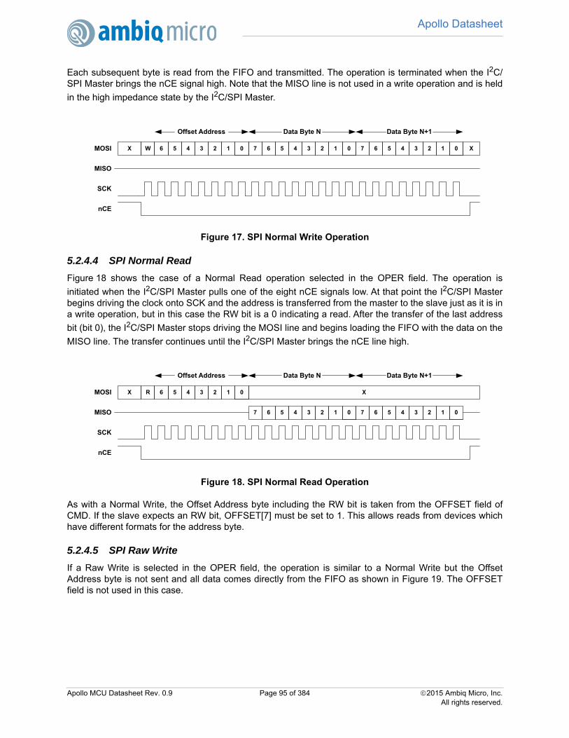
Apollo Datasheet
110
Each subsequent byte is read from the FIFO and transmitted. The operation is terminated when the I2C/SPI Master brings the nCE signal high. Note that the MISO line is not used in a write operation and is held
in the high impedance state by the I2C/SPI Master.
Figure 17. SPI Normal Write Operation
5.2.4.4 SPI Normal Read
Figure 18 shows the case of a Normal Read operation selected in the OPER field. The operation is
initiated when the I2C/SPI Master pulls one of the eight nCE signals low. At that point the I2C/SPI Masterbegins driving the clock onto SCK and the address is transferred from the master to the slave just as it is ina write operation, but in this case the RW bit is a 0 indicating a read. After the transfer of the last address
bit (bit 0), the I2C/SPI Master stops driving the MOSI line and begins loading the FIFO with the data on the
MISO line. The transfer continues until the I2C/SPI Master brings the nCE line high.
Figure 18. SPI Normal Read Operation
As with a Normal Write, the Offset Address byte including the RW bit is taken from the OFFSET field ofCMD. If the slave expects an RW bit, OFFSET[7] must be set to 1. This allows reads from devices whichhave different formats for the address byte.
5.2.4.5 SPI Raw Write
If a Raw Write is selected in the OPER field, the operation is similar to a Normal Write but the OffsetAddress byte is not sent and all data comes directly from the FIFO as shown in Figure 19. The OFFSETfield is not used in this case.
W 6 1MOSI
SCK
0 7 6 1 0
Offset Address
nCE
X
Data Byte N
7 6 1 0
Data Byte N+1
X
MISO
5 4 3 2 5 4 3 2 5 4 3 2
R 6 1MOSI
SCK
0
Offset Address
nCE
X
Data Byte N Data Byte N+1
7 6 1 0 7 6 1 0MISO
X5 4 3 2
5 4 3 2 5 4 3 2
Apollo MCU Datasheet Rev. 0.9 Page 95 of 384 2015 Ambiq Micro, Inc.All rights reserved.

Apollo Datasheet
110
Figure 19. SPI Raw Write Operation
5.2.4.6 SPI Raw Read
If a Raw Read is selected in the OPER field, the operation is simply the data transfer portion of a NormalRead. All data goes directly to the FIFO as shown in Figure 20. The OFFSET field is not used in this case.
Figure 20. SPI Raw Read Operation
5.2.4.7 Complex SPI Operations
In some cases peripheral devices require more complex transaction sequences than those supported by asingle Command. In order to support these transactions, the CONT bit may be set in the Command. In thiscase, the nCE pin selected by the Channel will remain asserted low at the end of the transaction, so thatthe next SPI operation will be seen as part of the same transaction. For example, there are peripheraldevices which require both a Function and an Address Offset to be transmitted at the beginning of a read.Implementing this can be done in several ways. One example as shown in Figure 21 is:
1. Execute a Raw SPI write of length 2, with the data bytes being the Function and Offset. Set the CONT bit in this Command so nCE remains asserted low.
2. Execute a Raw SPI Read of the desired transfer length. The data will then be read into the FIFO. The CONT bit is not set in this Command.
7 6 1MOSI
SCK
0 7 6 1 0
nCE
X 7 6 1 0
Data Byte N+2
X
MISO
5 4 3 2 5 4 3 2 5 4 3 2
Data Byte N+1Data Byte N
MOSI
SCK
nCE
Data Byte N+2
7 6 1 0 7 6 1 0MISO 5 4 3 2 5 4 3 2
Data Byte N+1
7 6 1 05 4 3 2
Data Byte N
Apollo MCU Datasheet Rev. 0.9 Page 96 of 384 2015 Ambiq Micro, Inc.All rights reserved.

Apollo Datasheet
110
Figure 21. SPI Combined Operation
5.2.4.8 SPI Polarity and Phase
The Apollo MCU supports all combinations of CPOL (clock polarity) and CPHA (data phase) in SPI mode,as defined by the SPOL and SPHA bits. Figure 22 shows how these two bits affect the interface signalbehavior.
Figure 22. SPI CPOL and CPHA
If CPOL is 0, the clock SCK is normally low and positive pulses are generated during transfers. If CPOL is1, SCK is normally high and negative pulses are generated during transfers.
If CPHA is 0, the data on the MOSI and MISO lines is sampled on the edge corresponding to the first SCKedge after nCE goes low (i.e. the rising edge if CPOL is 0 and the falling edge if CPOL is 1). Data on MISOand MOSI is driven on the opposite edge of SCK.
If CPHA is 1, the data on the MOSI and MISO lines is sampled on the edge corresponding to the secondSCK edge after nCE goes low (i.e. the falling edge if CPOL is 0 and the rising edge if CPOL is 1). Data onMISO and MOSI is driven on the opposite edge of SCK.
The SPOL and SPHA bits may be changed between Commands if different slave devices have differentrequirements. In this case the IFCEN bit should be set to 0 either before or at the same time as SPHA andSPOL are changed, and then set back to 1 before CMD is written.
7 6 1MOSI
SCK
0 7 6 1 0
Function
nCE
X
Offset Address
7 6 1 0
Read Data
X
MISO
5 4 3 2 5 4 3 2
5 4 3 2
Raw Write, 2 Bytes Raw Read, 1 Byte
CPOL=0
CPOL=1
7 6 1MOSI 0 7 6 1 0X 5 4 3 2 5 4 3 2
7 6 1MISO 0 7 6 1 0X 5 4 3 2 5 4 3 2
SCK
7 6 1MOSI 0 7 6 1 0X 5 4 3 2 5 4 3 2
7 6 1MISO 0 7 6 1 0X 5 4 3 2 5 4 3 2
CPHA=0
CPHA=1
X
X
X
X
SCK
nCE
Apollo MCU Datasheet Rev. 0.9 Page 97 of 384 2015 Ambiq Micro, Inc.All rights reserved.

Apollo Datasheet
110
5.2.5 Repeating a CommandSome peripherals, particularly sensors such as accelerometers and gyroscopes, have multiple registerswhich hold sample data (2 bytes each of X, Y and Z are common), and FIFOs behind these registers whichhold multiple samples. In order to allow software to retrieve several samples with a single operation, the
Apollo MCU I2C/SPI Master includes the capability to execute the same Command multiple times. Ifmultiple Commands are desired, the REG_IOMSTRn_CMDRPT Register is loaded with the number ofadditional times to execute the next Command (e.g. loading CMDRPT with the value 3 will cause the nextCommand to be executed a total of 4 times). When a Command is written to the Command Register, theCommand is then executed multiple times, filling or emptying the FIFO as appropriate. The series ofrepeated Commands behaves as if it was a single long Command, with a single CMDCMP interruptoccurring at the end and THR interrupts occurring if the FIFO crosses the relevant threshold. At the end ofany Command the CMDRPT Register has the value 0, so that single Commands may always be executedwithout requiring a write to CMDRPT.
As an example, assume the peripheral has 6 bytes of sensor sample data located at register offsets 10, 11,12, 13, 14 and 15. Also assume the internal FIFO threshold of the peripheral has been set so that aninterrupt occurs when the FIFO contains 8 samples. The CMDRPT register is set to 7, and a readCommand is executed with an offset of 10 and a length of 6. This Command will be executed 8 times, each
time bursting 6 bytes of data from registers 10-15 in the peripheral to the I2C/SPI Master FIFO. When
CMDCMP is received the FIFO in the I2C/SPI Master will contain 48 bytes of data. The bytes of data arepacked in the FIFO – there are no gaps between samples.
5.2.6 Bit Orientation
In both I2C and SPI modes, the I2C/SPI Master supports data transmission either LSB first or MSB first asconfigured by the LSB bit in the Command. If LSB is 0, data is transmitted and received MSB first. If LSB is1, data is transmitted and received LSB first.
5.2.7 Minimizing Power
Each I2C/SPI Master has a global interface enable bit REG_IOMSTRn_IOMCFG_IFCEN. This bit shouldbe kept at 0 whenever the interface is not being used in order to minimize power consumption. The FIFOcannot be accessed if IFCEN is 0, although all of the other registers are accessible. When the module isnot in use, the FSEL field should also be kept at 0 to minimize power. This is important even if IFCEN is a0.
Apollo MCU Datasheet Rev. 0.9 Page 98 of 384 2015 Ambiq Micro, Inc.All rights reserved.

Apollo Datasheet
110
5.3 IOMSTR RegistersI2C/SPI MasterINSTANCE 0 BASE ADDRESS:0x50004000
INSTANCE 1 BASE ADDRESS:0x50005000
5.3.1 Register Memory Map
Table 137: IOMSTR Register Map
Address(s) Register Name Description
0x500040000x50005000
FIFO FIFO Access Port
0x500041000x50005100
FIFOPTR Current FIFO Pointers
0x500041040x50005104
TLNGTH Transfer Length
0x500041080x50005108
FIFOTHR FIFO Threshold Configuration
0x5000410C0x5000510C
CLKCFG I/O Clock Configuration
0x500041100x50005110
CMD Command Register
0x500041140x50005114
CMDRPT Command Repeat Register
0x500041180x50005118
STATUS Status Register
0x5000411C0x5000511C
CFG I/O Master Configuration
0x500042000x50005200
INTEN IO Master Interrupts: Enable
0x500042040x50005204
INTSTAT IO Master Interrupts: Status
0x500042080x50005208
INTCLR IO Master Interrupts: Clear
0x5000420C0x5000520C
INTSET IO Master Interrupts: Set
Apollo MCU Datasheet Rev. 0.9 Page 99 of 384 2015 Ambiq Micro, Inc.All rights reserved.

Apollo Datasheet
110
5.3.2 IOMSTR Registers5.3.2.1 FIFO Register
FIFO Access Port
OFFSET: 0x00000000
INSTANCE 0 ADDRESS: 0x50004000
INSTANCE 1 ADDRESS: 0x50005000
FIFO Access Port
5.3.2.2 FIFOPTR Register
Current FIFO Pointers
OFFSET: 0x00000100
INSTANCE 0 ADDRESS: 0x50004100
INSTANCE 1 ADDRESS: 0x50005100
Current FIFO Pointers
Table 138: FIFO Register
31
30
29
28
27
26
25
24
23
22
21
20
19
18
17
16
15
14
13
12
11
10
09
08
07
06
05
04
03
02
01
00
FIFO
Table 139: FIFO Register Bits
Bit Name Reset RW Description
31:0 FIFO 0x0 RWFIFO access port.
Table 140: FIFOPTR Register
31
30
29
28
27
26
25
24
23
22
21
20
19
18
17
16
15
14
13
12
11
10
09
08
07
06
05
04
03
02
01
00
RSVD FIFOREM RSVD FIFOSIZ
Table 141: FIFOPTR Register Bits
Bit Name Reset RW Description
31:23 RSVD 0x0 RORESERVED
Apollo MCU Datasheet Rev. 0.9 Page 100 of 384 2015 Ambiq Micro, Inc.All rights reserved.

Apollo Datasheet
110
5.3.2.3 TLNGTH Register
Transfer Length
OFFSET: 0x00000104
INSTANCE 0 ADDRESS: 0x50004104
INSTANCE 1 ADDRESS: 0x50005104
Transfer Length
5.3.2.4 FIFOTHR Register
FIFO Threshold Configuration
OFFSET: 0x00000108
INSTANCE 0 ADDRESS: 0x50004108
INSTANCE 1 ADDRESS: 0x50005108
FIFO Threshold Configuration
22:16 FIFOREM 0x0 ROThe number of bytes remaining in the FIFO (i.e. 64-FIFOSIZ).
15:7 RSVD 0x0 RORESERVED
6:0 FIFOSIZ 0x0 ROThe number of bytes currently in the FIFO.
Table 142: TLNGTH Register
31
30
29
28
27
26
25
24
23
22
21
20
19
18
17
16
15
14
13
12
11
10
09
08
07
06
05
04
03
02
01
00
RSVD TLNGTH
Table 143: TLNGTH Register Bits
Bit Name Reset RW Description
31:12 RSVD 0x0 RORESERVED
11:0 TLNGTH 0x0 RORemaining transfer length.
Table 141: FIFOPTR Register Bits
Bit Name Reset RW Description
Apollo MCU Datasheet Rev. 0.9 Page 101 of 384 2015 Ambiq Micro, Inc.All rights reserved.

Apollo Datasheet
110
5.3.2.5 CLKCFG Register
I/O Clock Configuration
OFFSET: 0x0000010C
INSTANCE 0 ADDRESS: 0x5000410C
INSTANCE 1 ADDRESS: 0x5000510C
I/O Clock Configuration
Table 144: FIFOTHR Register
31
30
29
28
27
26
25
24
23
22
21
20
19
18
17
16
15
14
13
12
11
10
09
08
07
06
05
04
03
02
01
00
RSVD FIFOWTHR
RS
VD
FIFORTHR
Table 145: FIFOTHR Register Bits
Bit Name Reset RW Description
31:14 RSVD 0x0 RORESERVED
13:8 FIFOWTHR 0x0 RWFIFO write threshold.
7:6 RSVD 0x0 RORESERVED
5:0 FIFORTHR 0x0 RWFIFO read threshold.
Table 146: CLKCFG Register
31
30
29
28
27
26
25
24
23
22
21
20
19
18
17
16
15
14
13
12
11
10
09
08
07
06
05
04
03
02
01
00
TOTPER LOWPER RSVD
DIV
EN
DIV
3
FSEL RSVD
Table 147: CLKCFG Register Bits
Bit Name Reset RW Description
31:24 TOTPER 0x0 RWClock total count minus 1.
23:16 LOWPER 0x0 RWClock low count minus 1.
Apollo MCU Datasheet Rev. 0.9 Page 102 of 384 2015 Ambiq Micro, Inc.All rights reserved.

Apollo Datasheet
110
5.3.2.6 CMD Register
Command Register
OFFSET: 0x00000110
INSTANCE 0 ADDRESS: 0x50004110
INSTANCE 1 ADDRESS: 0x50005110
Command Register
15:13 RSVD 0x0 RORESERVED
12 DIVEN 0x0 RW
Enable clock division by TOTPER.
DIS = 0x0 - Disable TOTPER division.EN = 0x1 - Enable TOTPER division.
11 DIV3 0x0 RW
Enable divide by 3.
DIS = 0x0 - Select divide by 1.EN = 0x1 - Select divide by 3.
10:8 FSEL 0x0 RW
Select the input clock frequency.
HFRC_DIV64 = 0x0 - Selects the HFRC / 64 as the input clock.HFRC = 0x1 - Selects the HFRC as the input clock.HFRC_DIV2 = 0x2 - Selects the HFRC / 2 as the input clock.HFRC_DIV4 = 0x3 - Selects the HFRC / 4 as the input clock.HFRC_DIV8 = 0x4 - Selects the HFRC / 8 as the input clock.HFRC_DIV16 = 0x5 - Selects the HFRC / 16 as the input clock.HFRC_DIV32 = 0x6 - Selects the HFRC / 32 as the input clock.RSVD = 0x7 - Reserved.
7:0 RSVD 0x0 RORESERVED
Table 148: CMD Register
31
30
29
28
27
26
25
24
23
22
21
20
19
18
17
16
15
14
13
12
11
10
09
08
07
06
05
04
03
02
01
00
CMD
Table 147: CLKCFG Register Bits
Bit Name Reset RW Description
Apollo MCU Datasheet Rev. 0.9 Page 103 of 384 2015 Ambiq Micro, Inc.All rights reserved.

Apollo Datasheet
110
5.3.2.7 CMDRPT Register
Command Repeat Register
OFFSET: 0x00000114
INSTANCE 0 ADDRESS: 0x50004114
INSTANCE 1 ADDRESS: 0x50005114
Command Repeat Register
Table 149: CMD Register Bits
Bit Name Reset RW Description
31:0 CMD 0x0 RW
This register is the I/O Command.
POS_LENGTH = 0x0 - LSB bit position of the CMD LENGTH field.POS_OFFSET = 0x8 - LSB bit position of the CMD OFFSET field.POS_ADDRESS = 0x16 - LSB bit position of the I2C CMD ADDRESS field.POS_CHNL = 0x16 - LSB bit position of the SPI CMD CHANNEL field.POS_UPLNGTH = 0x23 - LSB bit position of the SPI CMD UPLNGTH field.POS_10BIT = 0x26 - LSB bit position of the I2C CMD 10-bit field.POS_LSB = 0x27 - LSB bit position of the CMD LSB-first field.POS_CONT = 0x28 - LSB bit position of the CMD CONTinue field.POS_OPER = 0x29 - LSB bit position of the CMD OPERation field.MSK_LENGTH = 0xFF - LSB bit mask of the CMD LENGTH field.MSK_OFFSET = 0xFF00 - LSB bit mask of the CMD OFFSET field.MSK_ADDRESS = 0xFF0000 - LSB bit mask of the I2C CMD ADDRESSfield.MSK_CHNL = 0x70000 - LSB bit mask of the SPI CMD CHANNEL field.MSK_UPLNGTH = 0x7800000 - LSB bit mask of the SPI CMD UPLNGTHfield.MSK_10BIT = 0x4000000 - LSB bit mask of the I2C CMD 10-bit field.MSK_LSB = 0x8000000 - LSB bit mask of the CMD LSB-first field.MSK_CONT = 0x10000000 - LSB bit mask of the CMD CONTinue field.MSK_OPER = 0xE0000000 - LSB bit mask of the CMD OPERation field.
Table 150: CMDRPT Register
31
30
29
28
27
26
25
24
23
22
21
20
19
18
17
16
15
14
13
12
11
10
09
08
07
06
05
04
03
02
01
00
RSVD CMDRPT
Table 151: CMDRPT Register Bits
Bit Name Reset RW Description
31:5 RSVD 0x0 RORESERVED
4:0 CMDRPT 0x0 RWThese bits hold the Command repeat count.
Apollo MCU Datasheet Rev. 0.9 Page 104 of 384 2015 Ambiq Micro, Inc.All rights reserved.

Apollo Datasheet
110
5.3.2.8 STATUS RegisterStatus Register
OFFSET: 0x00000118
INSTANCE 0 ADDRESS: 0x50004118
INSTANCE 1 ADDRESS: 0x50005118
Status Register
Table 152: STATUS Register
31
30
29
28
27
26
25
24
23
22
21
20
19
18
17
16
15
14
13
12
11
10
09
08
07
06
05
04
03
02
01
00
RSVD
IDLE
ST
CM
DA
CT
ER
R
Table 153: STATUS Register Bits
Bit Name Reset RW Description
31:3 RSVD 0x0 RORESERVED
2 IDLEST 0x0 ROThis bit indicates if the I/O state machine is IDLE.
IDLE = 0x1 - The I/O state machine is in the idle state.
1 CMDACT 0x0 ROThis bit indicates if the I/O Command is active.
ACTIVE = 0x1 - An I/O command is active.
0 ERR 0x0 ROThis bit indicates if an error interrupt has occurred.
ERROR = 0x1 - An error has been indicated by the IOM.
Apollo MCU Datasheet Rev. 0.9 Page 105 of 384 2015 Ambiq Micro, Inc.All rights reserved.

Apollo Datasheet
110
5.3.2.9 CFG RegisterI/O Master Configuration
OFFSET: 0x0000011C
INSTANCE 0 ADDRESS: 0x5000411C
INSTANCE 1 ADDRESS: 0x5000511C
I/O Master Configuration
Table 154: CFG Register
31
30
29
28
27
26
25
24
23
22
21
20
19
18
17
16
15
14
13
12
11
10
09
08
07
06
05
04
03
02
01
00
IFC
EN
RSVD
SP
HA
SP
OL
IFC
SE
L
Table 155: CFG Register Bits
Bit Name Reset RW Description
31 IFCEN 0x0 RW
This bit enables the IO Master.
DIS = 0x0 - Disable the IO Master.EN = 0x1 - Enable the IO Master.
30:3 RSVD 0x0 RORESERVED
2 SPHA 0x0 RW
This bit selects SPI phase.
SAMPLE_LEADING_EDGE = 0x0 - Sample on the leading (first) clockedge.SAMPLE_TRAILING_EDGE = 0x1 - Sample on the trailing (second) clockedge.
1 SPOL 0x0 RW
This bit selects SPI polarity.
CLK_BASE_0 = 0x0 - The base value of the clock is 0.CLK_BASE_1 = 0x1 - The base value of the clock is 1.
0 IFCSEL 0x0 RW
This bit selects the I/O interface.
I2C = 0x0 - Selects I2C interface for the I/O Master.SPI = 0x1 - Selects SPI interface for the I/O Master.
Apollo MCU Datasheet Rev. 0.9 Page 106 of 384 2015 Ambiq Micro, Inc.All rights reserved.

Apollo Datasheet
110
5.3.2.10 INTEN RegisterIO Master Interrupts: Enable
OFFSET: 0x00000200
INSTANCE 0 ADDRESS: 0x50004200
INSTANCE 1 ADDRESS: 0x50005200
Set bits in this register to allow this module to generate the corresponding interrupt.
Table 156: INTEN Register
31
30
29
28
27
26
25
24
23
22
21
20
19
18
17
16
15
14
13
12
11
10
09
08
07
06
05
04
03
02
01
00
RSVD
AR
B
ST
OP
STA
RT
ICM
D
IAC
C
WT
LE
N
NA
K
FO
VF
L
FU
ND
FL
TH
R
CM
DC
MP
Table 157: INTEN Register Bits
Bit Name Reset RW Description
31:11 RSVD 0x0 RORESERVED
10 ARB 0x0 RWThis is the arbitration loss interrupt.
9 STOP 0x0 RWThis is the STOP command interrupt.
8 START 0x0 RWThis is the START command interrupt.
7 ICMD 0x0 RWThis is the illegal command interrupt.
6 IACC 0x0 RWThis is the illegal FIFO access interrupt.
5 WTLEN 0x0 RWThis is the write length mismatch interrupt.
4 NAK 0x0 RWThis is the I2C NAK interrupt.
3 FOVFL 0x0 RWThis is the Read FIFO Overflow interrupt.
2 FUNDFL 0x0 RWThis is the Write FIFO Underflow interrupt.
1 THR 0x0 RWThis is the FIFO Threshold interrupt.
0 CMDCMP 0x0 RWThis is the Command Complete interrupt.
Apollo MCU Datasheet Rev. 0.9 Page 107 of 384 2015 Ambiq Micro, Inc.All rights reserved.

Apollo Datasheet
110
5.3.2.11 INTSTAT RegisterIO Master Interrupts: Status
OFFSET: 0x00000204
INSTANCE 0 ADDRESS: 0x50004204
INSTANCE 1 ADDRESS: 0x50005204
Read bits from this register to discover the cause of a recent interrupt.
Table 158: INTSTAT Register
31
30
29
28
27
26
25
24
23
22
21
20
19
18
17
16
15
14
13
12
11
10
09
08
07
06
05
04
03
02
01
00
RSVD
AR
B
ST
OP
STA
RT
ICM
D
IAC
C
WT
LE
N
NA
K
FO
VF
L
FU
ND
FL
TH
R
CM
DC
MP
Table 159: INTSTAT Register Bits
Bit Name Reset RW Description
31:11 RSVD 0x0 RORESERVED
10 ARB 0x0 RWThis is the arbitration loss interrupt.
9 STOP 0x0 RWThis is the STOP command interrupt.
8 START 0x0 RWThis is the START command interrupt.
7 ICMD 0x0 RWThis is the illegal command interrupt.
6 IACC 0x0 RWThis is the illegal FIFO access interrupt.
5 WTLEN 0x0 RWThis is the write length mismatch interrupt.
4 NAK 0x0 RWThis is the I2C NAK interrupt.
3 FOVFL 0x0 RWThis is the Read FIFO Overflow interrupt.
2 FUNDFL 0x0 RWThis is the Write FIFO Underflow interrupt.
1 THR 0x0 RWThis is the FIFO Threshold interrupt.
0 CMDCMP 0x0 RWThis is the Command Complete interrupt.
Apollo MCU Datasheet Rev. 0.9 Page 108 of 384 2015 Ambiq Micro, Inc.All rights reserved.

Apollo Datasheet
110
5.3.2.12 INTCLR RegisterIO Master Interrupts: Clear
OFFSET: 0x00000208
INSTANCE 0 ADDRESS: 0x50004208
INSTANCE 1 ADDRESS: 0x50005208
Write a 1 to a bit in this register to clear the interrupt status associated with that bit.
Table 160: INTCLR Register
31
30
29
28
27
26
25
24
23
22
21
20
19
18
17
16
15
14
13
12
11
10
09
08
07
06
05
04
03
02
01
00
RSVD
AR
B
ST
OP
STA
RT
ICM
D
IAC
C
WT
LE
N
NA
K
FO
VF
L
FU
ND
FL
TH
R
CM
DC
MP
Table 161: INTCLR Register Bits
Bit Name Reset RW Description
31:11 RSVD 0x0 RORESERVED
10 ARB 0x0 RWThis is the arbitration loss interrupt.
9 STOP 0x0 RWThis is the STOP command interrupt.
8 START 0x0 RWThis is the START command interrupt.
7 ICMD 0x0 RWThis is the illegal command interrupt.
6 IACC 0x0 RWThis is the illegal FIFO access interrupt.
5 WTLEN 0x0 RWThis is the write length mismatch interrupt.
4 NAK 0x0 RWThis is the I2C NAK interrupt.
3 FOVFL 0x0 RWThis is the Read FIFO Overflow interrupt.
2 FUNDFL 0x0 RWThis is the Write FIFO Underflow interrupt.
1 THR 0x0 RWThis is the FIFO Threshold interrupt.
0 CMDCMP 0x0 RWThis is the Command Complete interrupt.
Apollo MCU Datasheet Rev. 0.9 Page 109 of 384 2015 Ambiq Micro, Inc.All rights reserved.

Apollo Datasheet
110
5.3.2.13 INTSET RegisterIO Master Interrupts: Set
OFFSET: 0x0000020C
INSTANCE 0 ADDRESS: 0x5000420C
INSTANCE 1 ADDRESS: 0x5000520C
Write a 1 to a bit in this register to instantly generate an interrupt from this module. (Generally used fortesting purposes).
Table 162: INTSET Register
31
30
29
28
27
26
25
24
23
22
21
20
19
18
17
16
15
14
13
12
11
10
09
08
07
06
05
04
03
02
01
00
RSVD
AR
B
ST
OP
STA
RT
ICM
D
IAC
C
WT
LE
N
NA
K
FO
VF
L
FU
ND
FL
TH
R
CM
DC
MP
Table 163: INTSET Register Bits
Bit Name Reset RW Description
31:11 RSVD 0x0 RORESERVED
10 ARB 0x0 RWThis is the arbitration loss interrupt.
9 STOP 0x0 RWThis is the STOP command interrupt.
8 START 0x0 RWThis is the START command interrupt.
7 ICMD 0x0 RWThis is the illegal command interrupt.
6 IACC 0x0 RWThis is the illegal FIFO access interrupt.
5 WTLEN 0x0 RWThis is the write length mismatch interrupt.
4 NAK 0x0 RWThis is the I2C NAK interrupt.
3 FOVFL 0x0 RWThis is the Read FIFO Overflow interrupt.
2 FUNDFL 0x0 RWThis is the Write FIFO Underflow interrupt.
1 THR 0x0 RWThis is the FIFO Threshold interrupt.
0 CMDCMP 0x0 RWThis is the Command Complete interrupt.
Apollo MCU Datasheet Rev. 0.9 Page 110 of 384 2015 Ambiq Micro, Inc.All rights reserved.

Apollo Datasheet
138
6. I2C/SPI Slave Module
Figure 23. Block diagram for the I2C/SPI Slave Module
6.1 Functional Overview
The I2C/SPI Slave Module, shown in Figure 23, allows the Apollo MCU to function as a Slave in an I2C or
SPI system. The I2C/SPI Slave operates in an independent fashion, so that the Apollo MCU may be placedinto a sleep mode and still receive operations over the I/O interface. The Slave may be configured togenerate an interrupt on specific references.
The I2C/SPI Slave contains 256 bytes of RAM which is only accessible when the module is enabled. ThisRAM may be flexibly configured into three spaces: a block directly accessible via the I/O interface, a blockwhich functions as a FIFO for read operations on the interface, and a block of generally accessible RAMused to store parameters during deep sleep mode.
In I2C mode the Slave supports fully configurable 7 and 10-bit addressing and interface frequencies up to1.2 MHz. In SPI mode, the Slave supports all polarity/phase combinations and interface frequencies up to10 MHz.
6.2 Local RAM Allocation
The I2C/SPI Slave is built around a 256-byte local RAM (LRAM), through which all data flows between the
CPU AHB and the IO interface. The I2C/SPI Slave supports a 128-byte offset space when accessed fromthe I/O interface.
The LRAM is divided into three separate areas on 8-byte boundaries. These areas are:
I2C/SPI
Interface
To PinsIOSM
LRAM
Bus Interface
REQs
STALL
REQs
Regs
Counters,
Pointers
ADDR, WDATA
RDATA
ADDR,
WDATA
RDATA
IOINT
IOCLK
Apollo MCU Datasheet Rev. 0.9 Page 111 of 384 2015 Ambiq Micro, Inc.All rights reserved.

Apollo Datasheet
138
1. A Direct Area which is mapped between the AHB address space and the I/O address space. Thisarea is from LRAM address 0x00 to the address in the 5-bit configuration registerREG_IOSLAVE_FIFOCFG_FIFOBASE minus 1. FIFOBASE should be at most 0xF (120 bytes ofdirectly mapped locations).
2. A FIFO Area which is used to stream data from the Apollo MCU. This memory is directlyaddressed from the AHB, but accessed from the I/O Interface using a single I/O address 0x7F as astreaming port. The FIFO area is from the LRAM address in the FIFOBASE register to the LRAMaddress in the REG_IOSLAVE_FIFOCFG_FIFOMAX register minus 1.
3. A RAM Area which is accessible only from the AHB Slave. The RAM area is from the LRAMaddress in the FIFOMAX register to address 0xFF. The data in the LRAM is maintained in DeepSleep Mode.
Figure 24 below shows the LRAM address mapping between the I/O interface and the AHB. Note thatFIFOMAX may be set to 0x20, in which case there will be no RAM Area.
Figure 24. I2C/SPI Slave Module LRAM Addressing
6.3 Direct Area FunctionsThe Direct Area is used for direct communications between the interface Host and the Apollo MCU. TheHost may write a register in this space and read it back without requiring the CPU to wake up, so that verylow power interactions are supported. In most cases, however, some accesses require interaction with theCPU, so the Direct Area is further divided into three areas for CPU interaction.
I/O writes to locations 0x0-0xF will set a corresponding interrupt flag in the ACC_ISR register. Theselocations are typically used for specific commands to the Apollo MCU. Note that not all flags need generatean actual interrupt, so small multi-byte commands may be transmitted in this area.
I/O writes to locations 0x10 to 0x4F will set a corresponding interrupt flag in the ACC_ISR register if the I/Oaddress modulo 4 is 3 (i.e. addresses 0x13, 0x17, 0x1B, etc.). This allows larger transfers to be sent in aburst with a trigger being generated on the last write.
Up to 120 Bytes
Directly
Addressable
FIFO Data
0x00
0x7E/7F
I/O Address
FIFO Count H0x7C
FIFO Count L
Direct Area
RAM/AHB
0x00
FIFO Area
RAM Area
0x7D
0xFF
IOINT Regs
FIFOBASE * 8
FIFOMAX * 8
FIFOBASE * 8 - 1
0x78-7B
Apollo MCU Datasheet Rev. 0.9 Page 112 of 384 2015 Ambiq Micro, Inc.All rights reserved.

Apollo Datasheet
138
The ACC_ISR register includes 32 individual write interrupts, so the REG_IOSLAVE_PRENC registerprovides a priority encode of these interrupts to speed software decoding. The highest priority is bit 31 (seton access to address 0x00), and the lowest priority is bit 0 (set on access to address 0x4F).The third special area is a read-only area, which is from I/O addresses(REG_IOSLAVE_FIFOCFG_ROBASE * 8) to (FIFOBASE * 8 – 1). I/O writes to this address space will notchange the LRAM, which allows the space to be used for returning status to the I/O Host.
6.4 FIFO Area FunctionsThe FIFO is used to provide very efficient flow of data from the Apollo MCU to the I/O Host processor withminimal CPU interactions. A FIFO of up to 1023 bytes can be easily maintained by software, with theoldest bytes residing in the LRAM FIFO Area and the newer data being held in system SRAM and
transferred to the I2C/SPI Slave on demand. Several hardware features support this operation.
Figure 25 shows the basic FIFO operation. The main FIFO is held in a buffer in SRAM, and the oldest datain that FIFO has been transferred to the FIFO Area of the I/O Slave. TheREG_IOSLAVE_FIFOPTR_FIFOPTR register points to the next byte to be read on the I/O interface.
REG_IOSLAVE_FIFOPTR_FIFOSIZ holds the current number of valid bytes in the FIFO on the I2C/SPISlave, and FIFOCTR holds the total number of bytes in the FIFO. REG_IOSLAVE_FIFOCTR may be readat any time by the Host processor at offset 0x7C/D to determine if there is FIFO data available (and howmuch is currently in the FIFO).
Figure 25. I2C/SPI Slave Module FIFO
When the host reads a byte from the FIFO, the data retrieved is pointed to by FIFOPTR, FIFOPTR isincremented and wraps around in the FIFO Area if it reaches FIFOMAX. FIFOSIZ and FIFOCTR are eachdecremented by one. The Host can read FIFOCTR and then read that many bytes without furtherchecking. Note that this process can continue without requiring a CPU wakeup. If the Host attempts to read
the FIFO when FIFOSIZ is 0, the FUNDFL interrupt flag is set in both the I2C Slave interrupt block and inthe Host interrupt block.
FIFO Buffer in
SRAM
Local FIFOFIFO Area in
LRAM
FIFOPTRCur DataFIFO Read
Data @ 0x7F
FIFOSIZ
FIFOTHR
Compare FIFO Int
Decrement on
FIFO Read
Increment on
FIFO area
Write
FIFOCNTDecrement on
FIFO Read
Add value on write
to FIFOINC
Read at 0x7C/
0x7D
Apollo MCU Datasheet Rev. 0.9 Page 113 of 384 2015 Ambiq Micro, Inc.All rights reserved.
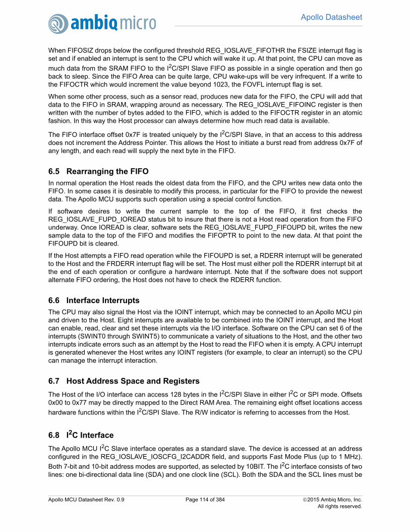
Apollo Datasheet
138
When FIFOSIZ drops below the configured threshold REG_IOSLAVE_FIFOTHR the FSIZE interrupt flag isset and if enabled an interrupt is sent to the CPU which will wake it up. At that point, the CPU can move asmuch data from the SRAM FIFO to the I2C/SPI Slave FIFO as possible in a single operation and then goback to sleep. Since the FIFO Area can be quite large, CPU wake-ups will be very infrequent. If a write tothe FIFOCTR which would increment the value beyond 1023, the FOVFL interrupt flag is set.
When some other process, such as a sensor read, produces new data for the FIFO, the CPU will add thatdata to the FIFO in SRAM, wrapping around as necessary. The REG_IOSLAVE_FIFOINC register is thenwritten with the number of bytes added to the FIFO, which is added to the FIFOCTR register in an atomicfashion. In this way the Host processor can always determine how much read data is available.
The FIFO interface offset 0x7F is treated uniquely by the I2C/SPI Slave, in that an access to this addressdoes not increment the Address Pointer. This allows the Host to initiate a burst read from address 0x7F ofany length, and each read will supply the next byte in the FIFO.
6.5 Rearranging the FIFOIn normal operation the Host reads the oldest data from the FIFO, and the CPU writes new data onto theFIFO. In some cases it is desirable to modify this process, in particular for the FIFO to provide the newestdata. The Apollo MCU supports such operation using a special control function.
If software desires to write the current sample to the top of the FIFO, it first checks theREG_IOSLAVE_FUPD_IOREAD status bit to insure that there is not a Host read operation from the FIFOunderway. Once IOREAD is clear, software sets the REG_IOSLAVE_FUPD_FIFOUPD bit, writes the newsample data to the top of the FIFO and modifies the FIFOPTR to point to the new data. At that point theFIFOUPD bit is cleared.
If the Host attempts a FIFO read operation while the FIFOUPD is set, a RDERR interrupt will be generatedto the Host and the FRDERR interrupt flag will be set. The Host must either poll the RDERR interrupt bit atthe end of each operation or configure a hardware interrupt. Note that if the software does not supportalternate FIFO ordering, the Host does not have to check the RDERR function.
6.6 Interface InterruptsThe CPU may also signal the Host via the IOINT interrupt, which may be connected to an Apollo MCU pinand driven to the Host. Eight interrupts are available to be combined into the IOINT interrupt, and the Hostcan enable, read, clear and set these interrupts via the I/O interface. Software on the CPU can set 6 of theinterrupts (SWINT0 through SWINT5) to communicate a variety of situations to the Host, and the other twointerrupts indicate errors such as an attempt by the Host to read the FIFO when it is empty. A CPU interruptis generated whenever the Host writes any IOINT registers (for example, to clear an interrupt) so the CPUcan manage the interrupt interaction.
6.7 Host Address Space and Registers
The Host of the I/O interface can access 128 bytes in the I2C/SPI Slave in either I2C or SPI mode. Offsets0x00 to 0x77 may be directly mapped to the Direct RAM Area. The remaining eight offset locations access
hardware functions within the I2C/SPI Slave. The R/W indicator is referring to accesses from the Host.
6.8 I2C Interface
The Apollo MCU I2C Slave interface operates as a standard slave. The device is accessed at an addressconfigured in the REG_IOSLAVE_IOSCFG_I2CADDR field, and supports Fast Mode Plus (up to 1 MHz).
Both 7-bit and 10-bit address modes are supported, as selected by 10BIT. The I2C interface consists of twolines: one bi-directional data line (SDA) and one clock line (SCL). Both the SDA and the SCL lines must be
Apollo MCU Datasheet Rev. 0.9 Page 114 of 384 2015 Ambiq Micro, Inc.All rights reserved.

Apollo Datasheet
138
connected to a positive supply voltage via a pull-up resistor. By definition, a device that sends a messageis called the “transmitter”, and the device that accepts the message is called the “receiver”. The device thatcontrols the message transfer by driving SCL is called “master”. The devices that are controlled by themaster are called “slaves”. The Apollo MCU I2C Slave is always a slave device.
The following protocol has been defined:
Data transfer may be initiated only when the bus is not busy. During data transfer, the data line must remain stable whenever the clock line is high. Changes in the data line while the clock line is high will be interpreted as control signals.
A number of bus conditions have been defined (see Figure 26) and are described in the following sections.
Figure 26. Basic I2C Conditions
6.8.1 Bus Not Busy
Both SDA and SCL remain high.
6.8.2 Start Data Transfer
A change in the state of SDA from high to low, while SCL is high, defines the START condition. A STARTcondition which occurs after a previous START but before a STOP is called a RESTART condition, andfunctions exactly like a normal STOP followed by a normal START.
6.8.3 Stop Data Transfer
A change in the state of SDA from low to high, while SCL is high, defines the STOP condition.
6.8.4 Data Valid
After a START condition, SDA is stable for the duration of the high period of SCL. The data on SDA may bechanged during the low period of SCL. There is one clock pulse per bit of data. Each data transfer isinitiated with a START condition and terminated with a STOP condition. The number of data bytestransferred between the START and STOP conditions is not limited. The information is transmitted byte-wide and each receiver acknowledges with a ninth bit.
6.8.5 Acknowledge
Each byte of eight bits is followed by one Acknowledge (ACK) bit as shown in Figure 27. ThisAcknowledge bit is a low level driven onto SDA by the receiver, whereas the master generates an extraACK related SCL pulse. A slave receiver which is addressed is obliged to generate an Acknowledge afterthe reception of each byte. Also, on a read transfer a master receiver must generate an Acknowledge afterthe reception of each byte that has been clocked out of the slave transmitter. The device thatacknowledges must pull down the SDA line during the Acknowledge clock pulse in such a way that theSDA line is a stable low during the high period of the Acknowledge related SCL pulse. A master receiver
SDA
SCL
START SDA Stable
SDA may
change
STOP
Not Busy
Apollo MCU Datasheet Rev. 0.9 Page 115 of 384 2015 Ambiq Micro, Inc.All rights reserved.

Apollo Datasheet
138
must signal an end-of-data to the slave transmitter by not generating an Acknowledge (a NAK) on the lastbyte that has been clocked out of the slave. In this case, the transmitter must leave the data line high toenable the master to generate the STOP condition.Figure 27. I2C Acknowledge
6.8.6 Address Operation
In I2C mode, the I2C/SPI Slave supports either 7-bit or 10-bit addressing, selected by the 10BIT bit in theIOSCFG Register. Figure 28 shows the operation in 7-bit mode in which the master addresses the ApolloMCU with a 7-bit address configured as 0xD2 in the I2CADDR field. After the START condition, the 7-bitaddress is transmitted MSB first. If this address matches the lower 7 bits of the I2CADDR field, the ApolloMCU is selected, the eighth bit indicate a write (RW = 0) or a read (RW = 1) operation and the Apollo MCUsupplies the ACK. The Apollo MCU ignores all other address values and does not respond with an ACK.
Figure 28. I2C 7-bit Address Operation
Figure 28 shows the operation with which the master addresses the Apollo MCU with a 10-bit addressconfigured at 0x536. After the START condition, the 10-bit preamble 0b11110 is transmitted first, followedby the first two address bits and the eighth bit indicating a write (RW = 0) or a read (RW = 1) operation. If
the upper two bits match the I2CADDR value, the I2C/SPI Slave supplies the ACK. The next transferincludes the lower 8 bits of the address, and if these bits also match I2CADDR the Apollo MCU again
supplies the ACK. The I2C/SPI Slave ignores all other address values and does not respond with an ACK.
Figure 29. I2C 10-bit Address Operation
6.8.7 Offset Address Transmission
If the RW bit of the Address Operation indicates a write, the next byte transmitted from the master is the
Offset Address as shown in Figure 30. This value is loaded into the Address Pointer of the I2C/SPI Slave.
SDA
SCL
START
MSB (bit 7) Bit 6 Bit 0 ACK
1 2 8 9
A1 1 0SDA
SCL
R
W0 1 0 0
A1 1 0SDA
SCL
R
WA1 0 1 11 1 0 1 0 1 1 0
Apollo MCU Datasheet Rev. 0.9 Page 116 of 384 2015 Ambiq Micro, Inc.All rights reserved.

Apollo Datasheet
138
Figure 30. I2C Offset Address Transmission
6.8.8 Write Operation
In a write operation the master transmitter transmits to the Apollo MCU slave receiver. The AddressOperation has a RW value of 0, and the second byte contains the Offset Address as in Figure 30. The nextbyte is written to the register selected by the Address Pointer (which was loaded with the Offset Address)and the Address Pointer is incremented. Subsequent transfers write bytes into successive registers until aSTOP condition is received, as shown in Figure 31. Note that if the Address Pointer is at 0x7F, it will notincrement on the write.
Figure 31. I2C Write Operation
6.8.9 Read Operation
In a read operation, the master first executes an Offset Address Transmission to load the Address Pointerwith the desired Offset Address. A subsequent operation will again issue the address of the Apollo MCUbut with the RW bit as a 1 indicating a read operation. Figure 32 shows this transaction beginning with aRESTART condition, although a STOP followed by a START may also be used. After the addressoperation, the slave becomes the transmitter and sends the register value from the location pointed to bythe Address Pointer, and the Address Pointer is incremented. Subsequent transactions producesuccessive register values, until the master receiver responds with a NAK and a STOP to complete theoperation. Because the Address Pointer holds a valid register address, the master may initiate anotherread sequence at this point without performing another Offset Address operation. Note that if the AddressPointer is at 0x7F, it will not increment on the read.
Figure 32. I2C Read Operation
A1 1 0SDA
SCL
0 A7 6 1 0
Offset Address
0 1 0 0 5 4 3 2
Addr OffsetSDA
SCL
7 0
Byte N
AW A A 7 0
Byte N+1
A 7 0
Byte N+2
A
SDA
SCL
7 0
Byte N
A A 7 0
Byte N+1
NAddr AR
RESTART
Addr OffsetAW
Apollo MCU Datasheet Rev. 0.9 Page 117 of 384 2015 Ambiq Micro, Inc.All rights reserved.

Apollo Datasheet
138
6.8.10 General Address DetectionThe I2C/SPI Slave may be configured to detect an I2C General Address (0x00) write. If this address isdetected, the first data byte written is stored in the REG_IOSLAVE_GADATA Register and the GENADinterrupt flag is set. This allows software to create the appropriate response, which is typically to reset the
I2C/SPI Slave.
6.9 SPI Interface
The I2C/SPI Slave includes a standard 3-wire or 4-wire SPI interface. The serial peripheral interface (SPI)bus is intended for synchronous communication between different ICs. 4-wire SPI consists of four signallines: serial data input (MOSI), serial data output (MISO), serial clock (SCL) and an active low chip enable
(nCE). The I2C/SPI Slave may be connected to a master with a 3-wire SPI interface by configuring 3-wiremode in the pin configuration block of the GPIO module, which will tie MOSI and MISO together. Bydefinition, a device that sends a message is called the “transmitter”, and the device that accepts themessage is called the “receiver”. The device that controls the message transfer by driving SCL is called
“master”. The devices that are controlled by the master are called “slaves”. The I2C/SPI Slave SPI Slave isalways a slave device.
The nCE input is used to initiate and terminate a data transfer. The SCL input is used to synchronize datatransfer between the master and the slave devices via the MOSI (master to slave) and MISO (slave tomaster) lines. The SCL input, which is generated by the master, is active only during address and datatransfer to any device on the SPI bus.
The I2C/SPI Slave supports clock frequencies up to 10 MHz, and responds to all SPI configurations ofCPOL and CPHA using the SPOL configuration bit. There is one clock for each bit transferred. Addressand data bits are transferred in groups of eight bits.
6.9.1 Write Operation
Figure 33 shows a SPI write operation. The operation is initiated when the nCE signal to the Apollo MCUgoes low. At that point an 8-bit Address byte is transmitted from the master on the MOSI line, with theupper RW bit indicating read (if 0) or write (if 1). In this example the RW bit is a one selecting a writeoperation, and the lower 7 bits of the Address byte contain the Offset Address, which is loaded into the
Address Pointer of the I2C/SPI Slave.
Each subsequent byte is loaded into the register selected by the Address Pointer, and the Address Pointeris incremented. The operation is terminated by the master by bringing the nCE signal high. Note that the
MISO line is not used in a write operation and is held in the high impedance state by the I2C/SPI Slave.Note also that if the Address Pointer is 0x7F, it does not increment on the read.
Figure 33. SPI Write Operation
W 6 1MOSI
SCK
0 7 6 1 0
Offset Address
nCE
X
Data Byte N
7 6 1 0
Data Byte N+1
X
MISO
5 4 3 2 5 4 3 2 5 4 3 2
Apollo MCU Datasheet Rev. 0.9 Page 118 of 384 2015 Ambiq Micro, Inc.All rights reserved.

Apollo Datasheet
138
6.9.2 Read OperationFigure 34 shows a read operation. The address is transferred from the master to the slave just as it is in awrite operation, but in this case the RW bit is a 0 indicating a read. After the transfer of the last address bit
(bit 0), the I2C/SPI Slave begins driving data from the register selected by the Address Pointer onto theMISO line, bit 7 first, and the Address Pointer is incremented. The transfer continues until the masterbrings the nCE line high. Note that if the Address Pointer is 0x7F, it does not increment on the read.
Figure 34. SPI Read Operation
6.9.3 Configuring 3-wire vs. 4-wire SPI Mode
The I2C/SPI Slave can operate in either 4-wire SPI mode, where the MISO and MOSI signals are onseparate wires, or in 3-wire SPI mode where MISO and MOSI share a wire. This configuration is performed
in the Pin Configuration module, and no configuration is necessary in the I2C/SPI Slave itself.
6.9.4 SPI Polarity and Phase
The I2C/SPI Slave supports all combinations of CPOL (clock polarity) and CPHA (data phase) in SPImode. Figure 35 shows how these two bits affect the interface signal behavior.
Figure 35. SPI CPOL and CPHA
R 6 1MOSI
SCK
0
Offset Address
nCE
X
Data Byte N Data Byte N+1
7 6 1 0 7 6 1 0MISO
X
5 4 3 2 5 4 3 2
5 4 3 2
CPOL=0
CPOL=1
7 6 1MOSI 0 7 6 1 0X 5 4 3 2 5 4 3 2
7 6 1MISO 0 7 6 1 0X 5 4 3 2 5 4 3 2
SCK
7 6 1MOSI 0 7 6 1 0X 5 4 3 2 5 4 3 2
7 6 1MISO 0 7 6 1 0X 5 4 3 2 5 4 3 2
CPHA=0
CPHA=1
X
X
X
X
SCK
nCE
Apollo MCU Datasheet Rev. 0.9 Page 119 of 384 2015 Ambiq Micro, Inc.All rights reserved.

Apollo Datasheet
138
If CPOL is 0, the clock SCK is normally low and positive pulses are generated during transfers. If CPOL is1, SCK is normally high and negative pulses are generated during transfers.If CPHA is 0, the data on the MOSI and MISO lines is sampled on the edge corresponding to the first SCKedge after nCE goes low (i.e. the rising edge if CPOL is 0 and the falling edge if CPOL is 1). Data on MISOand MOSI is driven on the opposite edge of SCK.
If CPHA is 1, the data on the MOSI and MISO lines is sampled on the edge corresponding to the secondSCK edge after nCE goes low (i.e. the falling edge if CPOL is 0 and the rising edge if CPOL is 1). Data onMISO and MOSI is driven on the opposite edge of SCK.
The I2C/SPI Slave has only a single SPOL bit to control the polarity. If CPOL = CPHA,REG_IOSLAVE_IOSCFG_SPOL must be set to 0. If CPOL ≠ CPHA, SPOL must be set to 1.
6.10 Bit Orientation
In both I2C and SPI modes, the I2C/SPI Slave supports data transmission either LSB first or MSB first asconfigured by the REG_IOSLAVE_IOSCFG_LSB bit. If LSB is 0, data is transmitted and received MSBfirst. If LSB is 1, data is transmitted and received LSB first.
6.11 Wakeup Using the I2C/SPI Slave
The I2C/SPI Slave can continue to operate even if the Apollo MCU CPU is in Sleep or Deep Sleep mode.
The hardware will enable and disable the I2C/SPI Slave clock and oscillators as necessary. The onlyconsideration in this environment is when the MCU is in a deep sleep mode, such that the HFRC Oscillator
is powered down, and a master attempts to access the I2C/SPI Slave. In this case the HFRC Oscillatormust be powered up before any is transferred to or from the internal RAM. This process takes roughly 5-10
us, and is initiated by nCE going low in SPI mode or by the detection of a START in I2C mode.
For I2C applications, the time delay is typically not relevant. At the fastest system clock of 1 MHz, themaster must transfer 9 bits of address plus 9 bits of offset before any FIFO access can occur, and that is aminimum of 18 us. The clocks will have started prior to that point in every case.
For SPI applications with fast interface clocks (faster than 1 MHz), the master must be programmed to pullnCE low at least 10 us prior to sending the first clock. If a master is unable to control the timing of nCE inthis way, then a GPIO interrupt can be configured to wake the Apollo MCU prior to initiating any SPItransfers.
There is no delay restriction if the MCU is in normal Sleep mode. In that case the HFRC is not powered
down and the I2C/SPI Slave clock will start immediately when nCE goes low.
Apollo MCU Datasheet Rev. 0.9 Page 120 of 384 2015 Ambiq Micro, Inc.All rights reserved.

Apollo Datasheet
138
6.12 IOSLAVE RegistersI2C/SPI SlaveINSTANCE 0 BASE ADDRESS:0x50000000
6.12.1 Register Memory Map
Table 164: IOSLAVE Register Map
Address(s) Register Name Description
0x50000100 FIFOPTR Current FIFO Pointer
0x50000104 FIFOCFG FIFO Configuration
0x50000108 FIFOTHR FIFO Threshold Configuration
0x5000010C FUPD FIFO Update Status
0x50000110 FIFOCTR Overall FIFO Counter
0x50000114 FIFOINC Overall FIFO Counter Increment
0x50000118 CFG I/O Slave Configuration
0x5000011C PRENC I/O Slave Interrupt Priority Encode
0x50000120 IOINTCTL I/O Interrupt Control
0x50000124 GENADD General Address Data
0x50000200 INTEN IO Slave Interrupts: Enable
0x50000204 INTSTAT IO Slave Interrupts: Status
0x50000208 INTCLR IO Slave Interrupts: Clear
0x5000020C INTSET IO Slave Interrupts: Set
0x50000210 REGACCINTEN Register Access Interrupts: Enable
0x50000214 REGACCINTSTAT Register Access Interrupts: Status
0x50000218 REGACCINTCLR Register Access Interrupts: Clear
0x5000021C REGACCINTSET Register Access Interrupts: Set
Apollo MCU Datasheet Rev. 0.9 Page 121 of 384 2015 Ambiq Micro, Inc.All rights reserved.

Apollo Datasheet
138
6.12.2 IOSLAVE Registers6.12.2.1 FIFOPTR Register
Current FIFO Pointer
OFFSET: 0x00000100
INSTANCE 0 ADDRESS: 0x50000100
Current FIFO Pointer
6.12.2.2 FIFOCFG Register
FIFO Configuration
OFFSET: 0x00000104
INSTANCE 0 ADDRESS: 0x50000104
FIFO Configuration
Table 165: FIFOPTR Register
31
30
29
28
27
26
25
24
23
22
21
20
19
18
17
16
15
14
13
12
11
10
09
08
07
06
05
04
03
02
01
00
RSVD FIFOSIZ FIFOPTR
Table 166: FIFOPTR Register Bits
Bit Name Reset RW Description
31:16 RSVD 0x0 RORESERVED
15:8 FIFOSIZ 0x0 RWThe number of bytes currently in the hardware FIFO.
7:0 FIFOPTR 0x0 RWCurrent FIFO pointer.
Table 167: FIFOCFG Register
31
30
29
28
27
26
25
24
23
22
21
20
19
18
17
16
15
14
13
12
11
10
09
08
07
06
05
04
03
02
01
00
RS
VD
ROBASE RSVD
RS
VD
FIFOMAX RSVD FIFOBASE
Apollo MCU Datasheet Rev. 0.9 Page 122 of 384 2015 Ambiq Micro, Inc.All rights reserved.

Apollo Datasheet
138
6.12.2.3 FIFOTHR Register
FIFO Threshold Configuration
OFFSET: 0x00000108
INSTANCE 0 ADDRESS: 0x50000108
FIFO Threshold Configuration
Table 168: FIFOCFG Register Bits
Bit Name Reset RW Description
31:30 RSVD 0x0 RORESERVED
29:24 ROBASE 0x20 RWDefines the read-only area. The IO Slave read-only area is situated inLRAM at (ROBASE*8) to (FIFOOBASE*8-1)
23:16 RSVD 0x0 RORESERVED
15:14 RSVD 0x0 RORESERVED
13:8 FIFOMAX 0x0 RW
These bits hold the maximum FIFO address in 8 byte segments. It is alsothe beginning of the RAM area of the LRAM. Note that no RAM area is con-figured if FIFOMAX is set to 0x1F.
7:5 RSVD 0x0 RORESERVED
4:0 FIFOBASE 0x0 RWThese bits hold the base address of the I/O FIFO in 8 byte segments.The IOSlave FIFO is situated in LRAM at (FIFOBASE*8) to (FIFOMAX*8-1).
Table 169: FIFOTHR Register
31
30
29
28
27
26
25
24
23
22
21
20
19
18
17
16
15
14
13
12
11
10
09
08
07
06
05
04
03
02
01
00
RSVD FIFOTHR
Table 170: FIFOTHR Register Bits
Bit Name Reset RW Description
31:8 RSVD 0x0 RORESERVED
7:0 FIFOTHR 0x0 RWFIFO size interrupt threshold.
Apollo MCU Datasheet Rev. 0.9 Page 123 of 384 2015 Ambiq Micro, Inc.All rights reserved.

Apollo Datasheet
138
6.12.2.4 FUPD RegisterFIFO Update Status
OFFSET: 0x0000010C
INSTANCE 0 ADDRESS: 0x5000010C
FIFO Update Status
6.12.2.5 FIFOCTR Register
Overall FIFO Counter
OFFSET: 0x00000110
INSTANCE 0 ADDRESS: 0x50000110
Overall FIFO Counter
Table 171: FUPD Register
31
30
29
28
27
26
25
24
23
22
21
20
19
18
17
16
15
14
13
12
11
10
09
08
07
06
05
04
03
02
01
00
RSVD
IOR
EA
D
FIF
OU
PD
Table 172: FUPD Register Bits
Bit Name Reset RW Description
31:2 RSVD 0x0 RORESERVED
1 IOREAD 0x0 ROThis bitfield indicates an IO read is active.
0 FIFOUPD 0x0 RWThis bit indicates that a FIFO update is underway.
Table 173: FIFOCTR Register
31
30
29
28
27
26
25
24
23
22
21
20
19
18
17
16
15
14
13
12
11
10
09
08
07
06
05
04
03
02
01
00
RSVD FIFOCTR
Table 174: FIFOCTR Register Bits
Bit Name Reset RW Description
31:10 RSVD 0x0 RORESERVED
Apollo MCU Datasheet Rev. 0.9 Page 124 of 384 2015 Ambiq Micro, Inc.All rights reserved.

Apollo Datasheet
138
6.12.2.6 FIFOINC Register
Overall FIFO Counter Increment
OFFSET: 0x00000114
INSTANCE 0 ADDRESS: 0x50000114
Overall FIFO Counter Increment
6.12.2.7 CFG Register
I/O Slave Configuration
OFFSET: 0x00000118
INSTANCE 0 ADDRESS: 0x50000118
I/O Slave Configuration
9:0 FIFOCTR 0x0 RWVirtual FIFO byte count
Table 175: FIFOINC Register
31
30
29
28
27
26
25
24
23
22
21
20
19
18
17
16
15
14
13
12
11
10
09
08
07
06
05
04
03
02
01
00
RSVD FIFOINC
Table 176: FIFOINC Register Bits
Bit Name Reset RW Description
31:10 RSVD 0x0 RORESERVED
9:0 FIFOINC 0x0 WOIncrement the Overall FIFO Counter by this value on a write
Table 177: CFG Register
31
30
29
28
27
26
25
24
23
22
21
20
19
18
17
16
15
14
13
12
11
10
09
08
07
06
05
04
03
02
01
00
IFC
EN
RSVD I2CADDR RSVD
STA
RT
RD
RS
VD
LSB
SP
OL
IFC
SE
L
Table 174: FIFOCTR Register Bits
Bit Name Reset RW Description
Apollo MCU Datasheet Rev. 0.9 Page 125 of 384 2015 Ambiq Micro, Inc.All rights reserved.

Apollo Datasheet
138
6.12.2.8 PRENC Register
I/O Slave Interrupt Priority Encode
OFFSET: 0x0000011C
INSTANCE 0 ADDRESS: 0x5000011C
I/O Slave Interrupt Priority Encode
Table 178: CFG Register Bits
Bit Name Reset RW Description
31 IFCEN 0x0 RW
IOSLAVE interface enable.
DIS = 0x0 - Disable the IOSLAVEEN = 0x1 - Enable the IOSLAVE
30:20 RSVD 0x0 RORESERVED
19:8 I2CADDR 0x0 RW7-bit or 10-bit I2C device address.
7:5 RSVD 0x0 RORESERVED
4 STARTRD 0x0 RW
This bit holds the cycle to initiate an I/O RAM read.
LATE = 0x0 - Initiate I/O RAM read late in each transferred byte.EARLY = 0x1 - Initiate I/O RAM read early in each transferred byte.
3 RSVD 0x0 RORESERVED
2 LSB 0x0 RW
This bit selects the transfer bit ordering.
MSB_FIRST = 0x0 - Data is assumed to be sent and received with MSBfirst.LSB_FIRST = 0x1 - Data is assumed to be sent and received with LSB first.
1 SPOL 0x0 RW
This bit selects SPI polarity.
SPI_MODES_0_3 = 0x0 - Polarity 0, handles SPI modes 0 and 3.SPI_MODES_1_2 = 0x1 - Polarity 1, handles SPI modes 1 and 2.
0 IFCSEL 0x0 RW
This bit selects the I/O interface.
I2C = 0x0 - Selects I2C interface for the IO Slave.SPI = 0x1 - Selects SPI interface for the IO Slave.
Table 179: PRENC Register
31
30
29
28
27
26
25
24
23
22
21
20
19
18
17
16
15
14
13
12
11
10
09
08
07
06
05
04
03
02
01
00
RSVD PRENC
Apollo MCU Datasheet Rev. 0.9 Page 126 of 384 2015 Ambiq Micro, Inc.All rights reserved.

Apollo Datasheet
138
6.12.2.9 IOINTCTL Register
I/O Interrupt Control
OFFSET: 0x00000120
INSTANCE 0 ADDRESS: 0x50000120
I/O Interrupt Control
Table 180: PRENC Register Bits
Bit Name Reset RW Description
31:5 RSVD 0x0 RORESERVED
4:0 PRENC 0x0 ROThese bits hold the priority encode of the REGACC interrupts.
Table 181: IOINTCTL Register
31
30
29
28
27
26
25
24
23
22
21
20
19
18
17
16
15
14
13
12
11
10
09
08
07
06
05
04
03
02
01
00
IOINTSET RSVD
IOIN
TC
LR
IOINT IOINTEN
Table 182: IOINTCTL Register Bits
Bit Name Reset RW Description
31:24 IOINTSET 0x0 WOThese bits set the IOINT interrupts when written with a 1.
23:17 RSVD 0x0 RORESERVED
16 IOINTCLR 0x0 WOThis bit clears all of the IOINT interrupts when written with a 1.
15:8 IOINT 0x0 ROThese bits read the IOINT interrupts.
7:0 IOINTEN 0x0 ROThese bits setread the IOINT interrupt enables.
Apollo MCU Datasheet Rev. 0.9 Page 127 of 384 2015 Ambiq Micro, Inc.All rights reserved.

Apollo Datasheet
138
6.12.2.10 GENADD RegisterGeneral Address Data
OFFSET: 0x00000124
INSTANCE 0 ADDRESS: 0x50000124
General Address Data
6.12.2.11 INTEN Register
IO Slave Interrupts: Enable
OFFSET: 0x00000200
INSTANCE 0 ADDRESS: 0x50000200
Set bits in this register to allow this module to generate the corresponding interrupt.
Table 183: GENADD Register
31
30
29
28
27
26
25
24
23
22
21
20
19
18
17
16
15
14
13
12
11
10
09
08
07
06
05
04
03
02
01
00
RSVD GADATA
Table 184: GENADD Register Bits
Bit Name Reset RW Description
31:8 RSVD 0x0 RORESERVED
7:0 GADATA 0x0 ROThe data supplied on the last General Address reference.
Table 185: INTEN Register
31
30
29
28
27
26
25
24
23
22
21
20
19
18
17
16
15
14
13
12
11
10
09
08
07
06
05
04
03
02
01
00
RSVD
IOIN
TW
GE
NA
D
FR
DE
RR
FU
ND
FL
FO
VF
L
FS
IZE
Table 186: INTEN Register Bits
Bit Name Reset RW Description
31:6 RSVD 0x0 RORESERVED
5 IOINTW 0x0 RWI2C Interrupt Write interrupt.
Apollo MCU Datasheet Rev. 0.9 Page 128 of 384 2015 Ambiq Micro, Inc.All rights reserved.
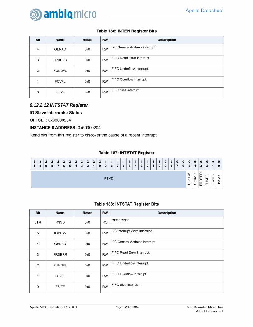
Apollo Datasheet
138
6.12.2.12 INTSTAT Register
IO Slave Interrupts: Status
OFFSET: 0x00000204
INSTANCE 0 ADDRESS: 0x50000204
Read bits from this register to discover the cause of a recent interrupt.
4 GENAD 0x0 RWI2C General Address interrupt.
3 FRDERR 0x0 RWFIFO Read Error interrupt.
2 FUNDFL 0x0 RWFIFO Underflow interrupt.
1 FOVFL 0x0 RWFIFO Overflow interrupt.
0 FSIZE 0x0 RWFIFO Size interrupt.
Table 187: INTSTAT Register
31
30
29
28
27
26
25
24
23
22
21
20
19
18
17
16
15
14
13
12
11
10
09
08
07
06
05
04
03
02
01
00
RSVD
IOIN
TW
GE
NA
D
FR
DE
RR
FU
ND
FL
FO
VF
L
FS
IZE
Table 188: INTSTAT Register Bits
Bit Name Reset RW Description
31:6 RSVD 0x0 RORESERVED
5 IOINTW 0x0 RWI2C Interrupt Write interrupt.
4 GENAD 0x0 RWI2C General Address interrupt.
3 FRDERR 0x0 RWFIFO Read Error interrupt.
2 FUNDFL 0x0 RWFIFO Underflow interrupt.
1 FOVFL 0x0 RWFIFO Overflow interrupt.
0 FSIZE 0x0 RWFIFO Size interrupt.
Table 186: INTEN Register Bits
Bit Name Reset RW Description
Apollo MCU Datasheet Rev. 0.9 Page 129 of 384 2015 Ambiq Micro, Inc.All rights reserved.

Apollo Datasheet
138
6.12.2.13 INTCLR RegisterIO Slave Interrupts: Clear
OFFSET: 0x00000208
INSTANCE 0 ADDRESS: 0x50000208
Write a 1 to a bit in this register to clear the interrupt status associated with that bit.
Table 189: INTCLR Register
31
30
29
28
27
26
25
24
23
22
21
20
19
18
17
16
15
14
13
12
11
10
09
08
07
06
05
04
03
02
01
00
RSVD
IOIN
TW
GE
NA
D
FR
DE
RR
FU
ND
FL
FO
VF
L
FS
IZE
Table 190: INTCLR Register Bits
Bit Name Reset RW Description
31:6 RSVD 0x0 RORESERVED
5 IOINTW 0x0 RWI2C Interrupt Write interrupt.
4 GENAD 0x0 RWI2C General Address interrupt.
3 FRDERR 0x0 RWFIFO Read Error interrupt.
2 FUNDFL 0x0 RWFIFO Underflow interrupt.
1 FOVFL 0x0 RWFIFO Overflow interrupt.
0 FSIZE 0x0 RWFIFO Size interrupt.
Apollo MCU Datasheet Rev. 0.9 Page 130 of 384 2015 Ambiq Micro, Inc.All rights reserved.

Apollo Datasheet
138
6.12.2.14 INTSET RegisterIO Slave Interrupts: Set
OFFSET: 0x0000020C
INSTANCE 0 ADDRESS: 0x5000020C
Write a 1 to a bit in this register to instantly generate an interrupt from this module. (Generally used fortesting purposes).
Table 191: INTSET Register
31
30
29
28
27
26
25
24
23
22
21
20
19
18
17
16
15
14
13
12
11
10
09
08
07
06
05
04
03
02
01
00
RSVD
IOIN
TW
GE
NA
D
FR
DE
RR
FU
ND
FL
FO
VF
L
FS
IZE
Table 192: INTSET Register Bits
Bit Name Reset RW Description
31:6 RSVD 0x0 RORESERVED
5 IOINTW 0x0 RWI2C Interrupt Write interrupt.
4 GENAD 0x0 RWI2C General Address interrupt.
3 FRDERR 0x0 RWFIFO Read Error interrupt.
2 FUNDFL 0x0 RWFIFO Underflow interrupt.
1 FOVFL 0x0 RWFIFO Overflow interrupt.
0 FSIZE 0x0 RWFIFO Size interrupt.
Apollo MCU Datasheet Rev. 0.9 Page 131 of 384 2015 Ambiq Micro, Inc.All rights reserved.

Apollo Datasheet
138
6.12.2.15 REGACCINTEN RegisterRegister Access Interrupts: Enable
OFFSET: 0x00000210
INSTANCE 0 ADDRESS: 0x50000210
Set bits in this register to allow this module to generate the corresponding interrupt.
6.12.2.16 REGACCINTSTAT Register
Register Access Interrupts: Status
OFFSET: 0x00000214
INSTANCE 0 ADDRESS: 0x50000214
Read bits from this register to discover the cause of a recent interrupt.
Table 193: REGACCINTEN Register
31
30
29
28
27
26
25
24
23
22
21
20
19
18
17
16
15
14
13
12
11
10
09
08
07
06
05
04
03
02
01
00
REGACC
Table 194: REGACCINTEN Register Bits
Bit Name Reset RW Description
31:0 REGACC 0x0 RWRegister access interrupts.
Table 195: REGACCINTSTAT Register
31
30
29
28
27
26
25
24
23
22
21
20
19
18
17
16
15
14
13
12
11
10
09
08
07
06
05
04
03
02
01
00
REGACC
Table 196: REGACCINTSTAT Register Bits
Bit Name Reset RW Description
31:0 REGACC 0x0 RWRegister access interrupts.
Apollo MCU Datasheet Rev. 0.9 Page 132 of 384 2015 Ambiq Micro, Inc.All rights reserved.

Apollo Datasheet
138
6.12.2.17 REGACCINTCLR RegisterRegister Access Interrupts: Clear
OFFSET: 0x00000218
INSTANCE 0 ADDRESS: 0x50000218
Write a 1 to a bit in this register to clear the interrupt status associated with that bit.
6.12.2.18 REGACCINTSET Register
Register Access Interrupts: Set
OFFSET: 0x0000021C
INSTANCE 0 ADDRESS: 0x5000021C
Write a 1 to a bit in this register to instantly generate an interrupt from this module. (Generally used fortesting purposes).
Table 197: REGACCINTCLR Register
31
30
29
28
27
26
25
24
23
22
21
20
19
18
17
16
15
14
13
12
11
10
09
08
07
06
05
04
03
02
01
00
REGACC
Table 198: REGACCINTCLR Register Bits
Bit Name Reset RW Description
31:0 REGACC 0x0 RWRegister access interrupts.
Table 199: REGACCINTSET Register
31
30
29
28
27
26
25
24
23
22
21
20
19
18
17
16
15
14
13
12
11
10
09
08
07
06
05
04
03
02
01
00
REGACC
Table 200: REGACCINTSET Register Bits
Bit Name Reset RW Description
31:0 REGACC 0x0 RWRegister access interrupts.
Apollo MCU Datasheet Rev. 0.9 Page 133 of 384 2015 Ambiq Micro, Inc.All rights reserved.

Apollo Datasheet
138
6.13 Host Side Address Space and Register6.13.1 Host Address Space and Registers
The Host of the I/O interface can access 128 bytes in the I2C/SPI Slave in either I2C or SPI mode. Offsets0x00 to 0x77 may be directly mapped to the Direct RAM Area. The remaining eight offset locations access
hardware functions within the I2C/SPI Slave. The R/W indicator refers to accesses from the Host.
6.13.1.1 HOST_IER Register
Host Interrupt Enable
OFFSET: 0x78
This register enables the FIFO read interrupts.
Table 201: HOST_IER Register
31
30
29
28
27
26
25
24
23
22
21
20
19
18
17
16
15
14
13
12
11
10
09
08
07
06
05
04
03
02
01
00
RSVD
FU
ND
FLE
N
RD
ER
RE
N
SW
INT
5EN
SW
INT
4EN
SW
INT
3EN
SW
INT
2EN
SW
INT
1EN
SW
INT
0EN
Table 202: HOST_IER Register Bits
Bit Name Reset RW Description
7 FUNDFLEN 0x0 RW If 1, enable an interrupt that triggers when the FIFO underflows
6 RDERREN 0x0 RWIf 1, enable the interrupt which occurs when the Host attempts to accessthe FIFO when read access is locked
5 SWINT5EN 0x0 RW If 1, enable software interrupt 5
4 SWINT4EN 0x0 RW If 1, enable software interrupt 4
3 SWINT3EN 0x0 RW If 1, enable software interrupt 3
2 SWINT2EN 0x0 RW If 1, enable software interrupt 2
1 SWINT1EN 0x0 RW If 1, enable software interrupt 1
0 SWINT0EN 0x0 RW If 1, enable software interrupt 0
Apollo MCU Datasheet Rev. 0.9 Page 134 of 384 2015 Ambiq Micro, Inc.All rights reserved.

Apollo Datasheet
138
6.13.1.2 HOST_ISR RegisterHost Interrupt Status Register
OFFSET: 0x79
The host uses this register to read interrupt status.
NOTE: All bits are cleared by a write to the IOINTCLR bit of the IOINTCTL Register.
6.13.1.3 HOST_WCR Register
Host Interrupt Write-to-Clear Register
OFFSET: 0x7A
Write a 1 to a bit in this register to clear a pending interrupt.
Table 203: HOST_ISR Register
31
30
29
28
27
26
25
24
23
22
21
20
19
18
17
16
15
14
13
12
11
10
09
08
07
06
05
04
03
02
01
00
RSVD
FU
ND
FLS
TAT
RD
ER
RS
TAT
SW
INT
5STA
T
SW
INT
4STA
T
SW
INT
3STA
T
SW
INT
2STA
T
SW
INT
1STA
T
SW
INT
0STA
T
Table 204: HOST_ISR Register Bits
Bit Name Reset RW Description
7 FUNDFLSTAT 0x0 ROThis bit is set by writing a 1 to bit 31 of the IOINTCTL Register, or if theHost attempts a FIFO read when FIFOCTR is 0.
6 RDERRSTAT 0x0 ROThis bit is set by writing a 1 to bit 30 of the IOINTCTL Register, or if theHost attempts a FIFO read when the FIFOUPD bit is a 1.
5 SWINT5STAT 0x0 RO This bit is set by writing a 1 to bit 29 of the IOINTCTL Register.
4 SWINT4STAT 0x0 RO This bit is set by writing a 1 to bit 28 of the IOINTCTL Register.
3 SWINT3STAT 0x0 RO This bit is set by writing a 1 to bit 27 of the IOINTCTL Register.
2 SWINT2STAT 0x0 RO This bit is set by writing a 1 to bit 26 of the IOINTCTL Register.
1 SWINT1STAT 0x0 RO This bit is set by writing a 1 to bit 25 of the IOINTCTL Register.
0 SWINT0STAT 0x0 RO This bit is set by writing a 1 to bit 24 of the IOINTCTL Register.
Table 205: HOST_WCR Register
31
30
29
28
27
26
25
24
23
22
21
20
19
18
17
16
15
14
13
12
11
10
09
08
07
06
05
04
03
02
01
00
RSVD
FU
ND
FLW
C
RD
ER
RW
C
SW
INT
5WC
SW
INT
4WC
SW
INT
3WC
SW
INT
2WC
SW
INT
1WC
SW
INT
0WC
Apollo MCU Datasheet Rev. 0.9 Page 135 of 384 2015 Ambiq Micro, Inc.All rights reserved.

Apollo Datasheet
138
6.13.1.4 HOST_WCS Register
Host Interrupt Write-to-Set Register
OFFSET: 0x7B
Write a 1 to a bit in this register to set the status bit of a pending interrupt.
Table 206: HOST_WCR Register Bits
Bit Name Reset RW Description
7 FUNDFLWC 0x0 WO Writing a 1 to this bit will clear the pending interrupt status bit FUNDFLSTAT
6 RDERRWC 0x0 WO Writing a 1 to this bit will clear the pending interrupt status bit RDERRSTAT
5 SWINT5WC 0x0 WO Writing a 1 to this bit will clear the pending interrupt status bit SWINT5STAT
4 SWINT4WC 0x0 WO Writing a 1 to this bit will clear the pending interrupt status bit SWINT4STAT
3 SWINT3WC 0x0 WO Writing a 1 to this bit will clear the pending interrupt status bit SWINT3STAT
2 SWINT2WC 0x0 WO Writing a 1 to this bit will clear the pending interrupt status bit SWINT2STAT
1 SWINT1WC 0x0 WO Writing a 1 to this bit will clear the pending interrupt status bit SWINT1STAT
0 SWINT0WC 0x0 WO Writing a 1 to this bit will clear the pending interrupt status bit SWINT0STAT
Table 207: HOST_WCS Register
31
30
29
28
27
26
25
24
23
22
21
20
19
18
17
16
15
14
13
12
11
10
09
08
07
06
05
04
03
02
01
00
RSVDF
UN
DF
LWS
RD
ER
RW
S
SW
INT
5WS
SW
INT
4WS
SW
INT
3WS
SW
INT
2WS
SW
INT
1WS
SW
INT
0WS
Table 208: HOST_WCS Register Bits
Bit Name Reset RW Description
7 FUNDFLWS 0x0 WO Writing a 1 to this bit will set the pending interrupt status bit FUNDFLSTAT
6 RDERRWS 0x0 WO Writing a 1 to this bit will set the pending interrupt status bit RDERRSTAT
5 SWINT5WS 0x0 WO Writing a 1 to this bit will set the pending interrupt status bit SWINT5STAT
4 SWINT4WS 0x0 WO Writing a 1 to this bit will set the pending interrupt status bit SWINT4STAT
3 SWINT3WS 0x0 WO Writing a 1 to this bit will set the pending interrupt status bit SWINT3STAT
2 SWINT2WS 0x0 WO Writing a 1 to this bit will set the pending interrupt status bit SWINT2STAT
1 SWINT1WS 0x0 WO Writing a 1 to this bit will set the pending interrupt status bit SWINT1STAT
0 SWINT0WS 0x0 WO Writing a 1 to this bit will set the pending interrupt status bit SWINT0STAT
Apollo MCU Datasheet Rev. 0.9 Page 136 of 384 2015 Ambiq Micro, Inc.All rights reserved.

Apollo Datasheet
138
6.13.1.5 FIFOCTRLO RegisterFIFOCTR Low Byte
OFFSET: 0x7C
This register allows the host to read the lower eight bits of the FIFOCTR register.
6.13.1.6 FIFOCTRUP Register
FIFOCTR Upper Byte
OFFSET: 0x7D
This register allows the host to read the upper two bits of the FIFOCTR register.
Table 209: FIFOCTRLO Register
31
30
29
28
27
26
25
24
23
22
21
20
19
18
17
16
15
14
13
12
11
10
09
08
07
06
05
04
03
02
01
00
RSVD FIFOCTRLO
Table 210: FIFOCTRLO Register Bits
Bit Name Reset RW Description
7:0 FIFOCTRLO 0x0 RO Reads the lower eight bits of FIFOCTR
Table 211: FIFOCTRUP Register
31
30
29
28
27
26
25
24
23
22
21
20
19
18
17
16
15
14
13
12
11
10
09
08
07
06
05
04
03
02
01
00
RSVD
FIF
OC
TR
UP
Table 212: FIFOCTRUP Register Bits
Bit Name Reset RW Description
1:0 FIFOCTRUP 0x0 RO Reads the upper two bits of FIFOCTR
Apollo MCU Datasheet Rev. 0.9 Page 137 of 384 2015 Ambiq Micro, Inc.All rights reserved.

Apollo Datasheet
138
6.13.1.7 FIFO RegisterFIFO Read Data
OFFSET: 0x7F
Read this register for FIFO data.
Table 213: FIFO Register
31
30
29
28
27
26
25
24
23
22
21
20
19
18
17
16
15
14
13
12
11
10
09
08
07
06
05
04
03
02
01
00
RSVD FIFO
Table 214: FIFO Register Bits
Bit Name Reset RW Description
7:0 FIFO 0x0 RO Reads the top byte of the FIFO
Apollo MCU Datasheet Rev. 0.9 Page 138 of 384 2015 Ambiq Micro, Inc.All rights reserved.

Apollo Datasheet
223
7. GPIO and Pad Configuration Module
Figure 36. Block diagram for the General Purpose I/O (GPIO) Module
7.1 Functional OverviewThe General Purpose I/O and Pad Configuration (GPIO) Module, shown in Figure 36, controls connectionsto up to 50 digital/analog pads. Each pad may be connected to a variety of module interface signals, withall pad input and output selection and control managed by the GPIO module. In addition, any pad mayfunction as a general purpose input and/or output pad which may be configured for a variety of externalfunctions. Each GPIO may be configured to generate an interrupt when a transition occurs on the input.
7.2 Pad Configuration FunctionsThe REG_GPIO_PADREGy (y = A to M) registers are used to control the function of each pad. Note thatthe REG_GPIO_PADKEY Register must be set to the value 0x73 in order to write the PADREGnRegisters. The REG_GPIO_PADREGy_PADnFNCSEL (n = 0 to 49) field selects one of up to eight signalsto be used for each pad, as shown in Table 215. Functions are grouped by module, with the color codingshown in Table 216. This table also defines the pad type for each configuration. The Special pad types aredefined in Table 217. Note that the CSP package only supports pads 0 through 21, 29, 31, 35, 36 and 41,which are shaded in orange in the Pad column of Table 215
The REG_GPIO_PADREGy_PADnSTRNG bit controls the drive strength of the pad. For all pads exceptfor pad 20, REG_GPIO_PADREGy_PADnPULL bit enables a weak pull-up on the pad when set to one.For pad 20, the REG_GPIO_PADREGy_PAD20PULL bit enables a weak pull-down on the pad when set toone. The REG_GPIO_PADREGy_PADnINPEN bit must be set to enable the pad input, and should be leftclear whenever the pad is not used in order to eliminate any leakage current in the pad.
Pads with a (*) (pads 3 and 4) have selectable high side power switch transistors to provide ~1 Ω switchesto VDDP. Pads with a (**) (pad 11) have selectable low side power switch transistors to provide ~1 Ωswitches to VSS. The high side power switches are enabled by setting theREG_GPIO_PADREGy_PAD3PWRUP or REG_GPIO_PADREGy_PAD4PWRUP bits, and the low sideswitch is enabled by setting the REG_GPIO_PADREGy_PAD11PWRDN bit. Once enabled, the switchesoperate in parallel with the normal pad function.
GPIO
Registers
Config
Registers
Bus
Interface
Digital
Pads
Config
Muxes
Other
Module
Signals
AHB
Apollo MCU Datasheet Rev. 0.9 Page 139 of 384 2015 Ambiq Micro, Inc.All rights reserved.

Apollo Datasheet
223
Pads 5, 6, 8 and 9 include optional pull-up resistors for use in I2C mode, to eliminate the need for externalresistors. If the pull-up is enabled by the PADnPULL bit, the REG_GPIO_PADREGy_PADnRSEL fieldselects the size of the pull-up resistor as shown in Table 218.
Table 215: Pad Function Mapping
PadPADnFNCSEL
0 1 2 3 4 5 6 70 SLSCL [I] SLSCK [I] UARTTX [O] GPIO0 M0SCK_LB M1SCK_LB M0SCL_LB M1SCL_LB1 SLSDA [S] SLMISO [O] UARTRX [I] GPIO1 M0MISO_LB M1MISO_LB M0SDA_LB M1SDA_LB2 SLWIR3 [S] SLMOSI [I] CLKOUT GPIO2 M0MOSI_LB M1MOSI_LB M0WIR3_LB M1WIR3_LB3* TRIG0 [I] SLnCE [O] M1nCE4 GPIO3 M0nCE_LB M1nCE_LB4* TRIG1 [I] SLINT [O] M0nCE5 GPIO4 SLINTGP_LB SWO [O] CLKOUT5 M0SCL [S] M0SCK[O] UARTS [O] GPIO5 M0SCK_LB M0SCL_LB6 M0SDA [S] M0MISO [I] UACTS [I] GPIO6 SLMISO_LB SLSDA_LB7 M0WIR3 [S] M0MOSI [O] CLKOUT GPIO7 SLWIR3_LB8 M1SCL [S] M1SCK [O] M0nCE4 GPIO8 M1SCK_LB M1SCL_LB9 M1SDA [S] M1MISO [I] M0nCE5 GPIO9 SLMISO_LB SLSDA_LB
10 M1WIR3 [S] M1MOSI [O] M0nCE6 GPIO10 SLWIR3_LB11** RESERVED M0nCE0 CLKOUT GPIO1112 ADC0 [A] M1nCE0 TCTA0 GPIO1213 ADC1 [A] M1nCE1 TCTB0 GPIO13 SWO [O]14 ADC2 [A] M1nCE2 UARTTX [O] GPIO1415 ADC3 [A] M1nCE3 UARTRX [I] GPIO1516 ADCREF [A] M0nCE4 TRIG2 [I] GPIO1617 CMPAD0 [A] M0nCE1 TRIG3 [I] GPIO17
18 CMPAD1 [A] M0nCE2 TCTA1 GPIO18
19 CMPRF0 [A] M0nCE3 TCTB1 GPIO1920 SWDCK [I] M1nCE5 TCTA2 GPIO2021 SWDIO [S] M1nCE6 TCTB2 GPIO2122 UARTTX [O] M1nCE7 TCTA3 GPIO2223 UARTRX [I] M0nCE0 TCTB3 GPIO2324 M0nCE1 CLKOUT GPIO2425 M0nCE2 TCTA0 GPIO2526 M0nCE3 TCTB0 GPIO2627 M1nCE4 TCTA1 GPIO2728 M1nCE5 TCTB1 GPIO2829 ADC4 [A] M1nCE6 TCTA2 GPIO2930 ADC5 [A] M1nCE7 TCTB2 GPIO3031 ADC6 [A] M0nCE4 TCTA3 GPIO3132 ADC7 [A] M0nCE5 TCTB3 GPIO3233 CMPRF1 [A] M0nCE6 GPIO3334 CMPRF2 [A] M0nCE7 GPIO3435 M1nCE0 UARTTX [O] GPIO3536 M1nCE1 UARTRX [I] GPIO3637 TRIG0 [I] M1nCE2 UARTS [O] GPIO3738 TRIG1 [I] M1nCE3 UACTS [I] GPIO3839 TRIG2 [I] UARTTX [O] CLKOUT GPIO3940 TRIG3 [I] UARTRX [I] GPIO4041 TRIG4 [I] SWO [O] GPIO4142 TRIG5 [I] M0nCE0 TCTA0 GPIO4243 TRIG6 [I] M0nCE1 TCTB0 GPIO4344 TRIG7 [I] M0nCE2 TCTA1 GPIO4445 M0nCE3 TCTB1 GPIO4546 M0nCE4 TCTA2 GPIO4647 M0nCE5 TCTB2 GPIO4748 M0nCE6 TCTA3 GPIO4849 M0nCE7 TCTB3 GPIO49
Apollo MCU Datasheet Rev. 0.9 Page 140 of 384 2015 Ambiq Micro, Inc.All rights reserved.

Apollo Datasheet
223
Table 216: Pad Function Color and Symbol Code
Color/Symbol
Function Pad Type
Various Supported on CSP package
ADC Signals Analog or Input, as indicated by [A] or [I] respectively
I2C/SPI Slave SignalsInput, Special or Push-pull output, as indicated by [I], [S] or[O] respectively,
I2C/SPI Master 0 SignalsInput, Special or Push-pull output, as indicated by [I], [S] or[O] respectively
I2C/SPI Master 1 SignalsInput, Special or Push-pull output, as indicated by [I], [S] or[O] respectively
GPIO Signals Controlled by GPIO Configuration
Counter/Timer Signals Controlled by CTIMER Configuration
UART SignalsInput or Push-pull output, as indicated by [I] or [O] respec-tively
CLKOUT Signals Push-pull Output
Loopback Connections Tri-state
Miscellaneous SignalsInput Special or Push-pull output, as indicated by [I], [S] or[O] respectively
* High-side power switchPads with a (*) (pads 3 and 4) have selectable high sidepower switch transistors to provide ~1 Ω switches to VDDP.
** Low-side power switchPads with a (**) (pad 11) have selectable low side powerswitch transistors to provide ~1 Ω switches to VSS.
Table 217: Special Pad Types
Pad PADnFNCSEL Name Pad Type
1 0 SLSDA Bidirectional Open Drain
2 0 SLWIR3 Bidirectional Tri-state
5 0 M0SCL Open Drain
6 0 M0SDA Bidirectional Open Drain
7 0 M0WIR3 Bidirectional Tri-state
8 0 M1SCL Open Drain
9 0 M1SDA Bidirectional Open Drain
10 0 M1WIR3 Bidirectional Tri-state
21 0 SWDIO Bidirectional Tri-state
Apollo MCU Datasheet Rev. 0.9 Page 141 of 384 2015 Ambiq Micro, Inc.All rights reserved.

Apollo Datasheet
223
7.3 General Purpose I/O (GPIO) FunctionsFor each pad, if the PADnFNCSEL field is set to 0x3 the pad is connected to the corresponding GPIOsignal. This section describes the configuration functions specific to GPIO pads.
7.3.1 Configuring the GPIO Functions
Each GPIO must be configured in the REG_GPIO_GPIOCFGy (y = A to G) Registers as an input and/oroutput. Note that the PADKEY Register must be set to the value 0x73 in order to write theREG_GPIO_GPIOCFGy Registers. Each output may be push-pull, open drain, disabled, or tri-stated asselected by the REG_GPIO_GPIOyCFG_GPIOnOUTCFG field. If the output is configured as push-pull,the pad will be driven with the corresponding bit in the GPIOWT Register. If the output is configured asopen drain, the pad will be pulled low if the corresponding bit in the GPIOWT Register is a 0, and will befloating if the corresponding bit in the GPIOWT Register is a 1. If the output is configured as tri-state, thepad will be driven with the corresponding bit in the GPIOWT Register if the corresponding bit in theGPIOEN Register is a 1. If the bit in GPIOEN is a 0, the output will be floating.
7.3.2 Reading from a GPIO Pad
All GPIO inputs are readable at all times, even if the pad is not configured as a GPIO. The current valuesof pads 0 to 31 are read in the GPIORDA Register, and the current values of pads 32 to 49 are read in theGPIORDB Register. If the GPIOnINCFG bit is set for a GPIO, it will always read as zero.
7.3.3 Writing to a GPIO Pad
The GPIO pad outputs are controlled by the GPIOWTA/B Registers and the GPIOENA/B Registers. Eachof these registers may be directly written and read. Because each GPIO is often an independent function,the capability also exists to set or clear one or more bits without having to perform a read-modify-writeoperation. If the GPIOWTSA or GPIOWTSB Register is written, the corresponding bit in GPIOWTA/B willbe set if the write data is 1, otherwise the GPIOWTA/B bit will not be changed. If the GPIOWTCA orGPIOWTCB Register is written, the corresponding bit in GPIOWTA/B will be cleared if the write data is 1,otherwise the GPIOWTA/B bit will not be changed.
If a GPIO pad is configured for tri-state output mode, the GPIOENA/B Register controls the enabling ofeach bit. GPIOENA and GPIOENB may be directly written, and individual bits may be set or cleared bywriting the GPIOENSA/B or GPIOENCA/B Registers with a 1 in the desired bit position.
7.3.4 GPIO Interrupts
Each GPIO pad can be configured to generate an interrupt on a high-to-low transition or a low-to-hightransition, as selected by the GPIOnINTP bit. This interrupt will be generated even if the pad is notconfigured as a GPIO in the Pad Configuration logic. Each interrupt is enabled, disabled, cleared or setwith a standard set of Interrupt Registers GPIOA_IER, GPIOA_ISR, GPIOA_WCR and GPIOB_WSR for
Table 218: I2C Pullup Resistor Selection
RSEL[1:0] Pullup Resistor
00 1.5 kΩ
01 6 kΩ
10 12 kΩ
11 24 kΩ
Apollo MCU Datasheet Rev. 0.9 Page 142 of 384 2015 Ambiq Micro, Inc.All rights reserved.

Apollo Datasheet
223
GPIO pads 0 to 31, and Registers GPIOB_IER, GPIOB_ISR, GPIOB_WCR and GPIOB_WSR for GPIOpads 32 to 49.7.4 Pad Connection Summary
Figure 37 shows the detailed implementation of each pad. Each element will be described in detail.
7.4.1 Output Selection
There is multiplexer (4 or 8 input depending upon the pad) which selects the module signal to be driven tothe output based on PADnFNCSEL. This implements the multiplexing shown in Table 215 for output pads.For all pads, a PADnFNCSEL value of 0x3 selects the value in the corresponding GPIOWT register bit.
7.4.2 Output Control
The pad driver for each pad has a data input and an output enable input. Each of these controls is selectedfrom among several alternatives based on the OUTDATSEL and OUTENSEL signals which are controlledby the selection of the output type as shown in Table 216 and Table 217.
OUTDATSEL normally selects the data from the output multiplexer, but if the pad is configured as OpenDrain the data input is selected to be low.
Apollo MCU Datasheet Rev. 0.9 Page 143 of 384 2015 Ambiq Micro, Inc.All rights reserved.

Apollo Datasheet
223
Figure 37. Pad Connection Details
OUTENSEL normally selects a ground signal to keep the pad driver enabled. If the pad is configured to beOpen Drain, the pad enable is driven with the data from the output multiplexer. If the pad is configured as aGPIO (PADnFNCSEL = 0x3) and the GPIO drive type is tri-state (GPIOnOUTCFG = 0x3), the pad enableis driven with the inverse of the corresponding GPIOEN bit. If the pad is not configured as an output, thepad enable is forced high to turn the driver off.
The drive strength of each pad driver is configured by the PADnSTRNG bit.
PAD
PADnFNCSEL
AND
GPIOnWT
GPIOnEN
Other Outputs
OUTENSEL
OUTDATSEL
PADnINPEN
ANDOR
GPIOnRD
PADnFNCSEL = 3
GPIOnINCFG
Other Input Muxes
XORINTGPIOnINT
GPIOnINTD
Analog
Connection
PADnFNCSEL = 0
PADnPULL
Mux
VDDP
PADnRSEL
VDDP
PADnSTRNG
AND
Apollo MCU Datasheet Rev. 0.9 Page 144 of 384 2015 Ambiq Micro, Inc.All rights reserved.

Apollo Datasheet
223
7.4.3 Input ControlThe input circuitry of the pad may be disabled by clearing the PADnINPEN bit. This configuration shouldalways be set if the pad input is not being used, as it prevents unnecessary current consumption if the padvoltage happens to float to a level between VDD and Ground. If PADnINPEN is 0, the pad will always readas a 0.
If PADnINPEN is set, the pad input then goes to two places. It is driven to the selected module signal asselected in Table 215. In addition, the pad input can always be read from the GPIORD register unless thepad is configured as a GPIO (PADnFNCSEL = 0x3) and GPIOnINCFG is high, which will force theGPIORD input to be a zero. The ability to always read the pad value is very useful in some diagnosticcases.
The pad input is always sent to the GPIO interrupt logic, and a pad transition in the direction selected byGPIOnINTD will set the corresponding GPIOn_INT flip-flop. Note that this interrupt will be set even if thepad is not configured as a GPIO, which may be useful in detecting functions. As an example, this could be
used to generate an interrupt when the I2C/SPI Slave nCE signal is driven low by the Interface Host.
7.4.4 Pull-up Control
If PADnPULL is high, a pullup resistor is connected between the pad and VDDP, except for pad 20, wherePADnPULL connects the resistor to VSS rather than VDDP.
The four pads which can be I2C/SPI Master output drivers (pads 5, 6, 8 and 9) contain the additionalcircuitry shown with the dashed lines. In this case four different pullup resistors are selected by thePADnRSEL field.
7.4.5 Analog Pad Configuration
Pads which may have Analog connections (pads 11-19 and 29-34) include the circuitry shown with thedotted lines. If the pad is configured in analog mode (PADnFNCSEL is 0x0), the pad is connected directlyto the particular analog module signal. In addition, OUTENSEL is forced high to disable the pad output,and the input of the pad is disabled independent of the value of PADnINPEN.
7.5 Module-specific Pad ConfigurationThe following sections describe in detail how to configure the pads for each module function.
7.5.1 Implementing IO Master Connections
The two IO Master modules must be correctly connected to the appropriate pads in order to operate.
7.5.1.1 IO Master 0 I2C Connection
I2C mode of IO Master 0 uses pad 5 as SCL and pad 6 as SDA. This mode is configured by setting thePADnFNCSEL fields as shown in Table 219. The PAD5INPEN and PAD6INPEN bits must be set. If the
internal I2C pullup resistors are to be used, PAD5PULL and PAD6PULL should be set, and the PAD5RSELand PAD6RSEL fields should be set to select the desired pullup resistor size as shown in Table 218. Ifexternal pullup resistors are used, PAD5PULL and PAD6PULL should be cleared.
Table 219: IO Master 0 I2C Configuration
Field Value
PAD5FNCSEL 0
PAD6FNCSEL 0
Apollo MCU Datasheet Rev. 0.9 Page 145 of 384 2015 Ambiq Micro, Inc.All rights reserved.

Apollo Datasheet
223
7.5.1.2 IO Master 1 I2C Connection
I2C mode of IO Master 1 uses pad 8 as SCL and pad 9 as SDA. This mode is configured by setting thePADnFNCSEL fields as shown in Table 220. The PAD8INPEN and PAD9INPEN bits must be set. If the
internal I2C pullup resistors are to be used, PAD8PULL and PAD9PULL should be set, and the PAD8RSELand PAD9RSEL fields should be set to select the desired pullup resistor size as shown in Table 218. Ifexternal pullup resistors are used, PAD8PULL and PAD9PULL should be cleared.
7.5.1.3 IO Master 0 4-wire SPI Connection
Four-wire SPI mode of IO Master 0 uses pad 5 as SCK, pad 6 as MISO and pad 7 as MOSI. This mode isconfigured by setting the PADnFNCSEL fields as shown in Table 221. The PAD5INPEN and PAD6INPENbits must be set. PAD5PULL, PAD6PULL and PAD7PULL should be cleared.
A variety of pads may be used for up to eight nCE signals to select up to eight separate slaves, as shownin Table 222. The PADnINPEN and PADnPULL bits of any pad used for nCE should be cleared.
Table 220: IO Master 1 I2C Configuration
Field Value
PAD8FNCSEL 0
PAD9FNCSEL 0
Table 221: IO Master 0 4-wire SPI Configuration
Field Value
PAD5FNCSEL 1
PAD6FNCSEL 1
PAD7FNCSEL 1
Apollo MCU Datasheet Rev. 0.9 Page 146 of 384 2015 Ambiq Micro, Inc.All rights reserved.

Apollo Datasheet
223
7.5.1.4 IO Master 1 4-wire SPI Connection
Four-wire SPI mode of IO Master 1 uses pad 8 as SCK, pad 9 as MISO and pad 10 as MOSI. This mode isconfigured by setting the PADnFNCSEL fields as shown in Table 223. The PAD8INPEN and PAD9INPENbits must be set. PAD8PULL, PAD9PULL and PAD10PULL should be cleared.
Table 222: IO Master 0 4-wire SPI nCE Configuration
Field Value nCE Selection Pad Used
PAD11FNCSEL 1 0 11
PAD23FNCSEL 1 0 23
PAD42FNCSEL 1 0 42
PAD17FNCSEL 1 1 17
PAD24FNCSEL 1 1 24
PAD43FNCSEL 1 1 43
PAD18FNCSEL 1 2 18
PAD25FNCSEL 1 2 25
PAD44FNCSEL 1 2 44
PAD19FNCSEL 1 3 19
PAD26FNCSEL 1 3 26
PAD45FNCSEL 1 3 45
PAD8FNCSEL 2 4 8
PAD16FNCSEL 1 4 16
PAD31FNCSEL 1 4 31
PAD46FNCSEL 1 4 46
PAD4FNCSEL 2 5 4
PAD9FNCSEL 2 5 9
PAD32FNCSEL 1 5 32
PAD47FNCSEL 1 5 47
PAD10FNCSEL 2 6 10
PAD33FNCSEL 1 6 33
PAD48FNCSEL 1 6 48
PAD34FNCSEL 1 7 34
PAD49FNCSEL 1 7 49
Table 223: IO Master 1 4-wire SPI Configuration
Field Value
PAD8FNCSEL 1
PAD9FNCSEL 1
PAD10FNCSEL 1
Apollo MCU Datasheet Rev. 0.9 Page 147 of 384 2015 Ambiq Micro, Inc.All rights reserved.

Apollo Datasheet
223
A variety of pads may be used for up to eight nCE signals to select up to eight separate slaves, as shownin Table 224. The PADnINPEN and PADnPULL bits of any pad used for nCE should be cleared.7.5.1.5 IO Master 0 3-wire SPI Connection
Three-wire SPI mode of IO Master 0 uses pad 5 as SCK and pad 7 as MOSI/MISO. This mode isconfigured by setting the PADnFNCSEL fields as shown in Table 225. The PAD5INPEN and PAD7INPENbits must be set. PAD5PULL and PAD7PULL should be cleared. Pad 6 may be used for other functions.
A variety of pads may be used for up to eight nCE signals to select up to eight separate slaves, as shownin Table 222. The PADnINPEN and PADnPULL bits of any pad used for nCE should be cleared.
Table 224: IO Master 1 4-wire SPI nCE Configuration
Field Value nCE Selection Pad Used
PAD12FNCSEL 1 0 12
PAD35FNCSEL 1 0 35
PAD13FNCSEL 1 1 13
PAD36FNCSEL 1 1 36
PAD14FNCSEL 1 2 14
PAD37FNCSEL 1 2 37
PAD15FNCSEL 1 3 15
PAD38FNCSEL 1 3 38
PAD3FNCSEL 2 4 3
PAD27FNCSEL 1 4 27
PAD20FNCSEL 2 5 20
PAD28FNCSEL 2 5 28
PAD21FNCSEL 2 6 21
PAD29FNCSEL 1 6 29
PAD22FNCSEL 1 7 22
PAD30FNCSEL 1 7 30
Table 225: IO Master 0 3-wire SPI Configuration
Field Value
PAD5FNCSEL 1
PAD7FNCSEL 0
Apollo MCU Datasheet Rev. 0.9 Page 148 of 384 2015 Ambiq Micro, Inc.All rights reserved.

Apollo Datasheet
223
7.5.1.6 IO Master 1 3-wire SPI ConnectionThree-wire SPI mode of IO Master 1 uses pad 8 as SCK and pad 10 as MOSI/MISO. This mode isconfigured by setting the PADnFNCSEL fields as shown in Table 226. The PAD8INPEN and PAD10INPENbits must be set. PAD8PULL and PAD10PULL should be cleared. Pad 9 may be used for other functions.
A variety of pads may be used for up to eight nCE signals to select up to eight separate slaves, as shownin Table 224. The PADnINPEN and PADnPULL bits of any pad used for nCE should be cleared.
7.5.2 Implementing IO Slave Connections
The IO Master module must be correctly connected to the appropriate pads in order to operate.
7.5.2.1 IO Slave I2C Connection
I2C mode of the IO Slave uses pad 0 as SCL and pad 1 as SDA. This mode is configured by setting thePADnFNCSEL fields as shown in Table 227. The PAD0INPEN and PAD1INPEN bits must be set.PAD0PULL and PAD1PULL should be cleared.
7.5.2.2 IO Slave 4-wire SPI Connection
Four-wire SPI mode of the IO Slave uses pad 0 as SCK, pad 1 as MISO, pad 2 as MOSI and pad 3 asnCE. This mode is configured by setting the PADnFNCSEL fields as shown in Table 228. ThePAD0INPEN, PAD2INPEN and PAD3INPEN bits must be set. PAD0PULL, PAD1PULL, PAD2PULL andPAD3PULL should be cleared.
7.5.2.3 IO Slave 3-wire SPI Connection
Three-wire SPI mode of the IO Slave uses pad 0 as SCK, pad 2 as MISO/MOSI and pad 3 as nCE. Thismode is configured by setting the PADnFNCSEL fields as shown in Table 229. The PAD0INPEN,
Table 226: IO Master 1 3-wire SPI Configuration
Field Value
PAD8FNCSEL 1
PAD10FNCSEL 0
Table 227: IO Slave I2C Configuration
Field Value
PAD0FNCSEL 0
PAD1FNCSEL 0
Table 228: IO Slave 4-wire SPI Configuration
Field Value
PAD0FNCSEL 1
PAD1FNCSEL 1
PAD2FNCSEL 1
PAD3FNCSEL 1
Apollo MCU Datasheet Rev. 0.9 Page 149 of 384 2015 Ambiq Micro, Inc.All rights reserved.

Apollo Datasheet
223
PAD2INPEN and PAD3INPEN bits must be set. PAD0PULL, PAD2PULL and PAD3PULL should becleared. Pad 1 may be used for other functions.7.5.2.4 IO Slave Interrupt Connection
The IO Slave can be configured to generate an interrupt output under a variety of internal conditions. If thisfunction is used, the interrupt will be generated on pad 4. PAD4FNCSEL must be set to 1, andPAD4INPEN and PAD4PULL should be cleared.
7.5.2.5 Implementing Internal I2C and SPI Loopback
The Pad Configuration module includes the capability of implementing internal loopback between the IO
Master and IO Slave modules in both I2C and SPI modes. This is useful for testing the Apollo MCU beforeconnecting to external devices. There are six loopback configurations.
7.5.2.6 IO Master 0 I2C Loopback
In this mode the IO Master 0 module drives the IO Slave in I2C mode. No pullup resistors are enabled, as
a logic function implements the wired-OR I2C function, so that all relevant PADnPULL bits should be set to0. This mode is enabled with the settings in Table 230. PADnINPEN must be set for all of the relevantpads.
7.5.2.7 IO Master 1 I2C Loopback
In this mode the IO Master 1 module drives the IO Slave in I2C mode. No pullup resistors are enabled, as
a logic function implements the wired-OR I2C function, so that all relevant PADnPULL bits should be set to0. This mode is enabled with the settings in Table 231. PADnINPEN must be set for all of the relevantpads.
Table 229: IO Slave 3-wire SPI Configuration
Field Value
PAD0FNCSEL 1
PAD2FNCSEL 0
PAD3FNCSEL 1
Table 230: IO Master 0 I2C Loopback
Field Value
PAD0FNCSEL 6
PAD1FNCSEL 6
PAD5FNCSEL 6
PAD6FNCSEL 6
Table 231: IO Master 1 I2C Loopback
Field Value
PAD0FNCSEL 7
PAD1FNCSEL 7
Apollo MCU Datasheet Rev. 0.9 Page 150 of 384 2015 Ambiq Micro, Inc.All rights reserved.

Apollo Datasheet
223
7.5.2.8 IO Master 0 4-wire SPI Loopback
In this mode the IO Master 0 module drives the IO Slave in 4-wire SPI mode. All relevant PADnPULL bitsshould be set to 0. This mode is enabled with the settings in Table 232. PADnINPEN must be set for all ofthe relevant pads.
7.5.2.9 IO Master 1 4-wire SPI Loopback
In this mode the IO Master 1 module drives the IO Slave in 4-wire SPI mode. All relevant PADnPULL bitsshould be set to 0. This mode is enabled with the settings in Table 233. PADnINPEN must be set for all ofthe relevant pads.
7.5.2.10 IO Master 0 3-wire SPI Loopback
In this mode the IO Master 0 module drives the IO Slave in 3-wire SPI mode. All relevant PADnPULL bitsshould be set to 0. This mode is enabled with the settings in Table 234. PADnINPEN must be set for all ofthe relevant pads.
PAD8FNCSEL 7
PAD9FNCSEL 7
Table 232: IO Master 0 4-wire SPI Loopback
Field Value
PAD0FNCSEL 4
PAD1FNCSEL 4
PAD2FNCSEL 4
PAD3FNCSEL 4
PAD5FNCSEL 4
PAD6FNCSEL 4
Table 233: IO Master 1 4-wire SPI Loopback
Field Value
PAD0FNCSEL 5
PAD1FNCSEL 5
PAD2FNCSEL 5
PAD3FNCSEL 5
PAD8FNCSEL 5
PAD9FNCSEL 5
Table 234: IO Master 0 3-wire SPI Loopback
Field Value
PAD0FNCSEL 4
Table 231: IO Master 1 I2C Loopback
Field Value
Apollo MCU Datasheet Rev. 0.9 Page 151 of 384 2015 Ambiq Micro, Inc.All rights reserved.

Apollo Datasheet
223
7.5.2.11 IO Master 1 3-wire SPI Loopback
In this mode the IO Master 1 module drives the IO Slave in 3-wire SPI mode. All relevant PADnPULL bitsshould be set to 0. This mode is enabled with the settings in Table 235. PADnINPEN must be set for all ofthe relevant pads.
7.5.2.12 IO Slave Interrupt Loopback
The interrupt output from the IO Slave may be looped back to a GPIO (GPIO4). This is accomplished bysetting PAD4FNCSEL to 4, and monitoring the interrupt output by reading GPIO4. PAD4INPEN must beset.
7.5.3 Implementing Counter/Timer Connections
Each Counter/Timer can optionally count pulses from an input pad, or generate pulses on an output pad.Table 236 shows the PADnFNCSEL settings to connect each Counter/Timer to the appropriate pad. If thepad is used as an input, the PADnINPEN bit should be set, otherwise it should be cleared. The PADnPULLbit may be set if the input signal is open drain.
PAD2FNCSEL 6
PAD3FNCSEL 4
PAD5FNCSEL 4
PAD7FNCSEL 6
Table 235: IO Master 1 3-wire SPI Loopback
Field Value
PAD0FNCSEL 5
PAD2FNCSEL 7
PAD3FNCSEL 5
PAD8FNCSEL 5
PAD10FNCSEL 7
Table 234: IO Master 0 3-wire SPI Loopback
Field Value
Apollo MCU Datasheet Rev. 0.9 Page 152 of 384 2015 Ambiq Micro, Inc.All rights reserved.

Apollo Datasheet
223
7.5.4 Implementing UART Connections
The UART signals can be connected to a variety of pads.
7.5.4.1 UART TX/RX Connections
The UART data signals TX and RX may each be connected to several pads. Note that TX and RX areselected independently. Table 237 shows the connections for TX, which should have the correspondingPADnINPEN and PADnPULL bits clear. Table 238 shows the connections for RX, which must have thecorresponding PADnINPEN bit set and should have the corresponding PADnPULL bit clear.
Table 236: Counter/Timer Pad Configuration
Field Value Ctr/Timer Pad
PAD12FNCSEL 2 A0 12
PAD25FNCSEL 2 A0 25
PAD42FNCSEL 2 A0 42
PAD13FNCSEL 2 B0 13
PAD26FNCSEL 2 B0 26
PAD43FNCSEL 2 B0 43
PAD18FNCSEL 2 A1 18
PAD27FNCSEL 2 A1 27
PAD44FNCSEL 2 A1 44
PAD19FNCSEL 2 B1 19
PAD28FNCSEL 2 B1 28
PAD45FNCSEL 2 B1 45
PAD20FNCSEL 2 A2 20
PAD29FNCSEL 2 A2 29
PAD46FNCSEL 2 A2 46
PAD21FNCSEL 2 B2 21
PAD30FNCSEL 2 B2 30
PAD47FNCSEL 2 B2 47
PAD22FNCSEL 2 A3 22
PAD31FNCSEL 2 A3 31
PAD48FNCSEL 2 A3 48
PAD23FNCSEL 2 B3 23
PAD32FNCSEL 2 B3 32
PAD49FNCSEL 2 B3 49
Apollo MCU Datasheet Rev. 0.9 Page 153 of 384 2015 Ambiq Micro, Inc.All rights reserved.

Apollo Datasheet
223
7.5.4.2 UART RTS/CTS Connections
The UART modem control signals RTS and CTS may each be connected to one of two pads. Note thatRTS and CTS are selected independently. Table 239 shows the connections for RTS, which should havethe corresponding PADnINPEN and PADnPULL bits clear. Table 240 shows the connections for CTS,which must have the corresponding PADnINPEN bit set and should have the corresponding PADnPULL bitclear.
7.5.5 Implementing GPIO Connections
Each pad of the Apollo MCU can be configured as a GPIO port by setting PADnFNCSEL to 3. PADnINPENand PADnPULL must be set appropriately depending on the specific GPIO function.
Table 237: UART TX Configuration
Field Value Pad
PAD0FNCSEL 2 0
PAD14FNCSEL 2 14
PAD22FNCSEL 0 22
PAD35FNCSEL 2 35
PAD39FNCSEL 1 39
Table 238: UART RX Configuration
Field Value Pad
PAD1FNCSEL 2 1
PAD15FNCSEL 2 15
PAD23FNCSEL 0 23
PAD36FNCSEL 2 36
PAD40FNCSEL 1 40
Table 239: UART RTS Configuration
Field Value Pad
PAD5FNCSEL 2 5
PAD37FNCSEL 2 37
Table 240: UART CTS Configuration
Field Value Pad
PAD6FNCSEL 2 6
PAD38FNCSEL 2 38
Apollo MCU Datasheet Rev. 0.9 Page 154 of 384 2015 Ambiq Micro, Inc.All rights reserved.

Apollo Datasheet
223
7.5.6 Implementing CLKOUT ConnectionsThe flexible clock output of the Clock Generator module, CLKOUT, may be configured on several pads asshown in Table 241. PADnINPEN and PADnPULL should be cleared in each case.
7.5.7 Implementing ADC Connections
Three types of pad connections may be made for the ADC module. Up to eight pads may be configured asthe analog inputs, as shown in Table 242. The ADCREF reference voltage input supplied on pad 16 isconfigured by setting PAD16FNCSEL to 0. If an external digital trigger is desired, up to eight selectable padchoices may be configured, as shown in Table 243. For the trigger inputs, PADnINPEN must be set. Forother inputs, PADnINPEN should be cleared. PADnPULL should be cleared except in the case of an opendrain trigger input.
Table 241: CLKOUT Configuration
Field Value Pad
PAD2FNCSEL 2 2
PAD4FNCSEL 6 4
PAD7FNCSEL 2 7
PAD11FNCSEL 2 11
PAD24FNCSEL 2 24
PAD39FNCSEL 2 39
Table 242: ADC Analog Input Configuration
Field Value Input Pad
PAD12FNCSEL 0 ADC0 12
PAD13FNCSEL 0 ADC1 13
PAD14FNCSEL 0 ADC2 14
PAD15FNCSEL 0 ADC3 15
PAD29FNCSEL 0 ADC4 29
PAD30FNCSEL 0 ADC5 30
PAD31FNCSEL 0 ADC6 31
PAD32FNCSEL 0 ADC7 32
Apollo MCU Datasheet Rev. 0.9 Page 155 of 384 2015 Ambiq Micro, Inc.All rights reserved.

Apollo Datasheet
223
7.5.8 Implementing Voltage Comparator Connections
Two types of pad connections may be made for the Voltage Comparator (VCOMP) module. Threereference voltages may be used for the comparator negative input as shown in Table 244. The voltage tobe applied to the comparator positive input are shown in Table 245. In each case PADnINPEN andPADnPULL should be cleared.
7.5.9 Implementing the Software Debug Port Connections
The software debug clock (SWDCK) and data (SWDIO) must be connected on pads 20 and 21respectively. PAD20FNCSEL and PAD21FNCSEL must be set to 0, PAD20INPEN and PAD21INPEN mustbe set, and PAD20PULL and PAD21PULL must be set, which results in a default state of SWDCK low and
Table 243: ADC Trigger Input Configuration
Field Value Input Pad
PAD3FNCSEL 0 TRIG0 3
PAD37FNCSEL 0 TRIG0 37
PAD4FNCSEL 0 TRIG1 4
PAD38FNCSEL 0 TRIG1 38
PAD16FNCSEL 0 TRIG2 16
PAD39FNCSEL 0 TRIG2 39
PAD17FNCSEL 0 TRIG3 17
PAD40FNCSEL 0 TRIG3 40
PAD41FNCSEL 0 TRIG4 41
PAD42FNCSEL 0 TRIG5 42
PAD43FNCSEL 0 TRIG6 43
PAD44FNCSEL 0 TRIG7 44
Table 244: Voltage Comparator Reference Configuration
Field Value Input Pad
PAD19FNCSEL 0 CMPRF0 19
PAD33FNCSEL 0 CMPRF1 33
PAD34FNCSEL 0 CMPRF2 34
Table 245: Voltage Comparator Input Configuration
Field Value Input Pad
PAD17FNCSEL 0 CMPIN0 17
PAD18FNCSEL 0 CMPIN1 18
Apollo MCU Datasheet Rev. 0.9 Page 156 of 384 2015 Ambiq Micro, Inc.All rights reserved.

Apollo Datasheet
223
SWDIO high. The optional continuous output signal SWO may be configured on a variety of pads asshown in Table 246, and PADnINPEN and PADnPULL should be cleared for the selected pad.7.6 GPIO RegistersGeneral Purpose IO
INSTANCE 0 BASE ADDRESS:0x40010000
This is the detailed description of the general purpose I/O (GPIO) block, as well as for the PAD multiplexor.Note that GPIO interrupt bits are edge triggered. WARNING: if an interrupt bit is cleared while thecombination of polarity and input are still asserted then this bit will not set again.
7.6.1 Register Memory Map
Table 246: SWO Configuration
Field Value Pad
PAD4FNCSEL 5 4
PAD13FNCSEL 6 13
PAD41FNCSEL 2 41
Table 247: GPIO Register Map
Address(s) Register Name Description
0x40010000 PADREGA Pad Configuration Register A
0x40010004 PADREGB Pad Configuration Register B
0x40010008 PADREGC Pad Configuration Register C
0x4001000C PADREGD Pad Configuration Register D
0x40010010 PADREGE Pad Configuration Register E
0x40010014 PADREGF Pad Configuration Register F
0x40010018 PADREGG Pad Configuration Register G
0x4001001C PADREGH Pad Configuration Register H
0x40010020 PADREGI Pad Configuration Register I
0x40010024 PADREGJ Pad Configuration Register J
0x40010028 PADREGK Pad Configuration Register K
0x4001002C PADREGL Pad Configuration Register L
0x40010030 PADREGM Pad Configuration Register M
0x40010040 CFGA GPIO Configuration Register A
0x40010044 CFGB GPIO Configuration Register B
0x40010048 CFGC GPIO Configuration Register C
0x4001004C CFGD GPIO Configuration Register D
0x40010050 CFGE GPIO Configuration Register E
0x40010054 CFGF GPIO Configuration Register F
0x40010058 CFGG GPIO Configuration Register G
0x40010060 PADKEY Key Register for all pad configuration registers
Apollo MCU Datasheet Rev. 0.9 Page 157 of 384 2015 Ambiq Micro, Inc.All rights reserved.

Apollo Datasheet
223
7.6.2 GPIO Registers
7.6.2.1 PADREGA Register
Pad Configuration Register A
OFFSET: 0x00000000
INSTANCE 0 ADDRESS: 0x40010000
This register controls the pad configuration controls for PAD3 through PAD0. Writes to this register must beunlocked by the PADKEY register.
0x40010080 RDA GPIO Input Register A
0x40010084 RDB GPIO Input Register B
0x40010088 WTA GPIO Output Register A
0x4001008C WTB GPIO Output Register B
0x40010090 WTSA GPIO Output Register A Set
0x40010094 WTSB GPIO Output Register B Set
0x40010098 WTCA GPIO Output Register A Clear
0x4001009C WTCB GPIO Output Register B Clear
0x400100A0 ENA GPIO Enable Register A
0x400100A4 ENB GPIO Enable Register B
0x400100A8 ENSA GPIO Enable Register A Set
0x400100AC ENSB GPIO Enable Register B Set
0x400100B4 ENCA GPIO Enable Register A Clear
0x400100B8 ENCB GPIO Enable Register B Clear
0x40010200 INT0EN GPIO Interrupt Registers 31-0: Enable
0x40010204 INT0STAT GPIO Interrupt Registers 31-0: Status
0x40010208 INT0CLR GPIO Interrupt Registers 31-0: Clear
0x4001020C INT0SET GPIO Interrupt Registers 31-0: Set
0x40010210 INT1EN GPIO Interrupt Registers 49-32: Enable
0x40010214 INT1STAT GPIO Interrupt Registers 49-32: Status
0x40010218 INT1CLR GPIO Interrupt Registers 49-32: Clear
0x4001021C INT1SET GPIO Interrupt Registers 49-32: Set
Table 247: GPIO Register Map
Address(s) Register Name Description
Apollo MCU Datasheet Rev. 0.9 Page 158 of 384 2015 Ambiq Micro, Inc.All rights reserved.

Apollo Datasheet
223
Table 248: PADREGA Register
31
30
29
28
27
26
25
24
23
22
21
20
19
18
17
16
15
14
13
12
11
10
09
08
07
06
05
04
03
02
01
00
PA
D3
PW
RU
P
RS
VD
PA
D3F
NC
SE
L
PA
D3S
TR
NG
PA
D3I
NP
EN
PA
D3P
ULL
RS
VD
PA
D2F
NC
SE
L
PA
D2S
TR
NG
PA
D2I
NP
EN
PA
D2P
ULL
RS
VD
PA
D1F
NC
SE
L
PA
D1S
TR
NG
PA
D1I
NP
EN
PA
D1P
ULL
RS
VD
PA
D0F
NC
SE
L
PA
D0S
TR
NG
PA
D0I
NP
EN
PA
D0P
ULL
Table 249: PADREGA Register Bits
Bit Name Reset RW Description
31 PAD3PWRUP 0x0 RW
Pad 3 upper power switch enable
DIS = 0x0 - Power switch disabledEN = 0x1 - Power switch enabled
30 RSVD 0x0 RORESERVED
29:27 PAD3FNCSEL 0x3 RW
Pad 3 function select
TRIG0 = 0x0 - Configure as the ADC Trigger 0 signalSLnCE = 0x1 - Configure as the IOSLAVE SPI nCE signalM1nCE4 = 0x2 - Configure as the SPI channel 4 nCE signal from IOMSTR1GPIO3 = 0x3 - Configure as GPIO3M0nCE = 0x4 - Configure as the IOSLAVE SPI nCE loopback signal fromIOMSTR0M1nCE = 0x5 - Configure as the IOSLAVE SPI nCE loopback signal fromIOMSTR1DIS = 0x6 - Pad disabled
26 PAD3STRNG 0x0 RW
Pad 3 drive strength.
LOW = 0x0 - Low drive strengthHIGH = 0x1 - High drive strength
25 PAD3INPEN 0x0 RW
Pad 3 input enable.
DIS = 0x0 - Pad input disabledEN = 0x1 - Pad input enabled
24 PAD3PULL 0x0 RW
Pad 3 pullup enable
DIS = 0x0 - Pullup disabledEN = 0x1 - Pullup enabled
23:22 RSVD 0x0 RORESERVED
Apollo MCU Datasheet Rev. 0.9 Page 159 of 384 2015 Ambiq Micro, Inc.All rights reserved.

Apollo Datasheet
223
21:19 PAD2FNCSEL 0x3 RW
Pad 2 function select
SLWIR3 = 0x0 - Configure as the IOSLAVE SPI 3-wire MOSI/MISO signalSLMOSI = 0x1 - Configure as the IOSLAVE SPI MOSI signalCLKOUT = 0x2 - Configure as the CLKOUT signalGPIO2 = 0x3 - Configure as GPIO2M0MOSI = 0x4 - Configure as the IOSLAVE SPI MOSI loopback signal fromIOMSTR0M1MOSI = 0x5 - Configure as the IOSLAVE SPI MOSI loopback signal fromIOMSTR1M0WIR3 = 0x6 - Configure as the IOSLAVE SPI 3-wire MOSI/MISO loop-back signal from IOMSTR0M1WIR3 = 0x7 - Configure as the IOSLAVE SPI 3-wire MOSI/MISO loop-back signal from IOMSTR1
18 PAD2STRNG 0x0 RW
Pad 2 drive strength
LOW = 0x0 - Low drive strengthHIGH = 0x1 - High drive strength
17 PAD2INPEN 0x0 RW
Pad 2 input enable
DIS = 0x0 - Pad input disabledEN = 0x1 - Pad input enabled
16 PAD2PULL 0x0 RW
Pad 2 pullup enable
DIS = 0x0 - Pullup disabledEN = 0x1 - Pullup enabled
15:14 RSVD 0x0 RORESERVED
13:11 PAD1FNCSEL 0x3 RW
Pad 1 function select
SLSDA = 0x0 - Configure as the IOSLAVE I2C SDA signalSLMISO = 0x1 - Configure as the IOSLAVE SPI MISO signalUARTRX = 0x2 - Configure as the UART RX signalGPIO1 = 0x3 - Configure as GPIO1M0MISO = 0x4 - Configure as the IOSLAVE SPI MISO loopback signal fromIOMSTR0M1MISO = 0x5 - Configure as the IOSLAVE SPI MISO loopback signal fromIOMSTR1M0SDA = 0x6 - Configure as the IOSLAVE I2C SDA loopback signal fromIOMSTR0M1SDA = 0x7 - Configure as the IOSLAVE I2C SDA loopback signal fromIOMSTR1
10 PAD1STRNG 0x0 RW
Pad 1 drive strength
LOW = 0x0 - Low drive strengthHIGH = 0x1 - High drive strength
9 PAD1INPEN 0x0 RW
Pad 1 input enable
DIS = 0x0 - Pad input disabledEN = 0x1 - Pad input enabled
8 PAD1PULL 0x0 RW
Pad 1 pullup enable
DIS = 0x0 - Pullup disabledEN = 0x1 - Pullup enabled
Table 249: PADREGA Register Bits
Bit Name Reset RW Description
Apollo MCU Datasheet Rev. 0.9 Page 160 of 384 2015 Ambiq Micro, Inc.All rights reserved.

Apollo Datasheet
223
7.6.2.2 PADREGB Register
Pad Configuration Register B
OFFSET: 0x00000004
INSTANCE 0 ADDRESS: 0x40010004
This register controls the pad configuration controls for PAD7 through PAD4. Writes to this register must beunlocked by the PADKEY register.
7:6 RSVD 0x0 RORESERVED
5:3 PAD0FNCSEL 0x3 RW
Pad 0 function select
SLSCL = 0x0 - Configure as the IOSLAVE I2C SCL signalSLSCK = 0x1 - Configure as the IOSLAVE SPI SCK signalUARTTX = 0x2 - Configure as the UART TX signalGPIO0 = 0x3 - Configure as GPIO0M0SCK = 0x4 - Configure as the IOSLAVE SPI SCK loopback signal fromIOMSTR0M1SCK = 0x5 - Configure as the IOSLAVE SPI SCK loopback signal fromIOMSTR1M0SCL = 0x6 - Configure as the IOSLAVE I2C SCL loopback signal fromIOMSTR0M1SCL = 0x7 - Configure as the IOSLAVE I2C SCL loopback signal fromIOMSTR1
2 PAD0STRNG 0x0 RW
Pad 0 drive strength
LOW = 0x0 - Low drive strengthHIGH = 0x1 - High drive strength
1 PAD0INPEN 0x0 RW
Pad 0 input enable
DIS = 0x0 - Pad input disabledEN = 0x1 - Pad input enabled
0 PAD0PULL 0x0 RW
Pad 0 pullup enable
DIS = 0x0 - Pullup disabledEN = 0x1 - Pullup enabled
Table 250: PADREGB Register
31
30
29
28
27
26
25
24
23
22
21
20
19
18
17
16
15
14
13
12
11
10
09
08
07
06
05
04
03
02
01
00
RS
VD
PA
D7F
NC
SE
L
PA
D7S
TR
NG
PA
D7I
NP
EN
PA
D7P
ULL
PA
D6
RS
EL
PA
D6F
NC
SE
L
PA
D6S
TR
NG
PA
D6I
NP
EN
PA
D6P
ULL
PA
D5
RS
EL
PA
D5F
NC
SE
L
PA
D5S
TR
NG
PA
D5I
NP
EN
PA
D5P
ULL
PA
D4P
WR
UP
RS
VD
PA
D4F
NC
SE
L
PA
D4S
TR
NG
PA
D4I
NP
EN
PA
D4P
ULL
Table 249: PADREGA Register Bits
Bit Name Reset RW Description
Apollo MCU Datasheet Rev. 0.9 Page 161 of 384 2015 Ambiq Micro, Inc.All rights reserved.

Apollo Datasheet
223
Table 251: PADREGB Register Bits
Bit Name Reset RW Description
31:30 RSVD 0x0 RORESERVED
29:27 PAD7FNCSEL 0x3 RW
Pad 7 function select
M0WIR3 = 0x0 - Configure as the IOMSTR0 SPI 3-wire MOSI/MISO signalM0MOSI = 0x1 - Configure as the IOMSTR0 SPI MOSI signalCLKOUT = 0x2 - Configure as the CLKOUT signalGPIO7 = 0x3 - Configure as GPIO7SLWIR3 = 0x6 - Configure as the IOMSTR0 SPI 3-wire MOSI/MISO loop-back signal from IOSLAVEDIS = 0x7 - Pad disabled
26 PAD7STRNG 0x0 RW
Pad 7 drive strentgh
LOW = 0x0 - Low drive strengthHIGH = 0x1 - High drive strength
25 PAD7INPEN 0x0 RW
Pad 7 input enable
DIS = 0x0 - Pad input disabledEN = 0x1 - Pad input enabled
24 PAD7PULL 0x0 RW
Pad 7 pullup enable
DIS = 0x0 - Pullup disabledEN = 0x1 - Pullup enabled
23:22 PAD6RSEL 0x0 RW
Pad 6 pullup resistor selection.
PULL1_5K = 0x0 - Pullup is ~1.5 KOhmsPULL6K = 0x1 - Pullup is ~6 KOhmsPULL12K = 0x2 - Pullup is ~12 KOhmsPULL24K = 0x3 - Pullup is ~24 KOhms
21:19 PAD6FNCSEL 0x3 RW
Pad 6 function select
M0SDA = 0x0 - Configure as the IOMSTR0 I2C SDA signalM0MISO = 0x1 - Configure as the IOMSTR0 SPI MISO signalUACTS = 0x2 - Configure as the UART CTS signalGPIO6 = 0x3 - Configure as GPIO6SLMISO = 0x4 - Configure as the IOMSTR0 SPI MISO loopback signal fromIOSLAVESLSDA = 0x6 - Configure as the IOMSTR0 I2C SDA loopback signal fromIOSLAVEDIS = 0x7 - Pad disabled
18 PAD6STRNG 0x0 RW
Pad 6 drive strength
LOW = 0x0 - Low drive strengthHIGH = 0x1 - High drive strength
17 PAD6INPEN 0x0 RW
Pad 6 input enable
DIS = 0x0 - Pad input disabledEN = 0x1 - Pad input enabled
16 PAD6PULL 0x0 RW
Pad 6 pullup enable
DIS = 0x0 - Pullup disabledEN = 0x1 - Pullup enabled
Apollo MCU Datasheet Rev. 0.9 Page 162 of 384 2015 Ambiq Micro, Inc.All rights reserved.

Apollo Datasheet
223
15:14 PAD5RSEL 0x0 RW
Pad 5 pullup resistor selection.
PULL1_5K = 0x0 - Pullup is ~1.5 KOhmsPULL6K = 0x1 - Pullup is ~6 KOhmsPULL12K = 0x2 - Pullup is ~12 KOhmsPULL24K = 0x3 - Pullup is ~24 KOhms
13:11 PAD5FNCSEL 0x3 RW
Pad 5 function select
M0SCL = 0x0 - Configure as the IOMSTR0 I2C SCL signalM0SCK = 0x1 - Configure as the IOMSTR0 SPI SCK signalUARTS = 0x2 - Configure as the UART RTS signalGPIO5 = 0x3 - Configure as GPIO5SLSCK = 0x4 - Configure as the IOMSTR0 SPI SCK loopback signal fromIOSLAVESLSCL = 0x6 - Configure as the IOMSTR0 I2C SCL loopback signal fromIOSLAVEDIS = 0x7 - Pad disabled
10 PAD5STRNG 0x0 RW
Pad 5 drive strength
LOW = 0x0 - Low drive strengthHIGH = 0x1 - High drive strength
9 PAD5INPEN 0x0 RW
Pad 5 input enable
DIS = 0x0 - Pad input disabledEN = 0x1 - Pad input enabled
8 PAD5PULL 0x0 RW
Pad 5 pullup enable
DIS = 0x0 - Pullup disabledEN = 0x1 - Pullup enabled
7 PAD4PWRUP 0x0 RW
Pad 4 upper power switch enable
DIS = 0x0 - Power switch disabledEN = 0x1 - Power switch enabled
6 RSVD 0x0 RORESERVED
5:3 PAD4FNCSEL 0x3 RW
Pad 4 function select
TRIG1 = 0x0 - Configure as the ADC Trigger 1 signalSLINT = 0x1 - Configure as the IOSLAVE interrupt out signalM0nCE5 = 0x2 - Configure as the SPI channel 5 nCE signal from IOMSTR0GPIO4 = 0x3 - Configure as GPIO4SLINTGP = 0x4 - Configure as the IOSLAVE interrupt loopback signal toGPIO4SWO = 0x5 - Configure as the serial wire debug SWO signalCLKOUT = 0x6 - Configure as the CLKOUT signalDIS = 0x7 - Pad disabled
2 PAD4STRNG 0x0 RW
Pad 4 drive strength
LOW = 0x0 - Low drive strengthHIGH = 0x1 - High drive strength
1 PAD4INPEN 0x0 RW
Pad 4 input enable
DIS = 0x0 - Pad input disabledEN = 0x1 - Pad input enabled
Table 251: PADREGB Register Bits
Bit Name Reset RW Description
Apollo MCU Datasheet Rev. 0.9 Page 163 of 384 2015 Ambiq Micro, Inc.All rights reserved.

Apollo Datasheet
223
7.6.2.3 PADREGC Register
Pad Configuration Register C
OFFSET: 0x00000008
INSTANCE 0 ADDRESS: 0x40010008
This register controls the pad configuration controls for PAD11 through PAD8. Writes to this register mustbe unlocked by the PADKEY register.
0 PAD4PULL 0x0 RW
Pad 4 pullup enable
DIS = 0x0 - Pullup disabledEN = 0x1 - Pullup enabled
Table 252: PADREGC Register
31
30
29
28
27
26
25
24
23
22
21
20
19
18
17
16
15
14
13
12
11
10
09
08
07
06
05
04
03
02
01
00
RS
VD
PA
D11
PW
RD
N
RS
VD
PA
D11
FN
CS
EL
PA
D11
ST
RN
G
PA
D11
INP
EN
PA
D11
PU
LL
RS
VD
PA
D10
FN
C-
SE
L
PA
D10
ST
RN
G
PA
D10
INP
EN
PA
D10
PU
LL
PA
D9R
SE
L
PA
D9F
NC
SE
L
PA
D9S
TR
NG
PA
D9I
NP
EN
PA
D9P
ULL
PA
D8R
SE
L
PA
D8F
NC
SE
L
PA
D8S
TR
NG
PA
D8I
NP
EN
PA
D8P
ULL
Table 253: PADREGC Register Bits
Bit Name Reset RW Description
31 RSVD 0x0 RORESERVED
30 PAD11PWRDN 0x0 RW
Pad 11 lower power switch enable
DIS = 0x0 - Power switch disabledEN = 0x1 - Power switch enabled
29 RSVD 0x0 RORESERVED
28:27 PAD11FNCSEL 0x3 RW
Pad 11 function select
ANATST = 0x0 - Configure as the analog test output signalM0nCE0 = 0x1 - Configure as the SPI channel 0 nCE signal from IOMSTR0CLKOUT = 0x2 - Configure as the CLKOUT signalGPIO11 = 0x3 - Configure as GPIO11
26 PAD11STRNG 0x0 RW
Pad 11 drive strentgh
LOW = 0x0 - Low drive strengthHIGH = 0x1 - High drive strength
Table 251: PADREGB Register Bits
Bit Name Reset RW Description
Apollo MCU Datasheet Rev. 0.9 Page 164 of 384 2015 Ambiq Micro, Inc.All rights reserved.
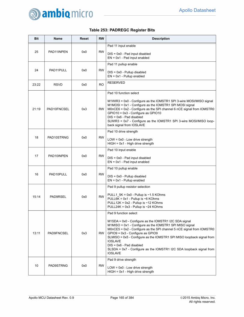
Apollo Datasheet
223
25 PAD11INPEN 0x0 RW
Pad 11 input enable
DIS = 0x0 - Pad input disabledEN = 0x1 - Pad input enabled
24 PAD11PULL 0x0 RW
Pad 11 pullup enable
DIS = 0x0 - Pullup disabledEN = 0x1 - Pullup enabled
23:22 RSVD 0x0 RORESERVED
21:19 PAD10FNCSEL 0x3 RW
Pad 10 function select
M1WIR3 = 0x0 - Configure as the IOMSTR1 SPI 3-wire MOSI/MISO signalM1MOSI = 0x1 - Configure as the IOMSTR1 SPI MOSI signalM0nCE6 = 0x2 - Configure as the SPI channel 6 nCE signal from IOMSTR0GPIO10 = 0x3 - Configure as GPIO10DIS = 0x6 - Pad disabledSLWIR3 = 0x7 - Configure as the IOMSTR1 SPI 3-wire MOSI/MISO loop-back signal from IOSLAVE
18 PAD10STRNG 0x0 RW
Pad 10 drive strength
LOW = 0x0 - Low drive strengthHIGH = 0x1 - High drive strength
17 PAD10INPEN 0x0 RW
Pad 10 input enable
DIS = 0x0 - Pad input disabledEN = 0x1 - Pad input enabled
16 PAD10PULL 0x0 RW
Pad 10 pullup enable
DIS = 0x0 - Pullup disabledEN = 0x1 - Pullup enabled
15:14 PAD9RSEL 0x0 RW
Pad 9 pullup resistor selection
PULL1_5K = 0x0 - Pullup is ~1.5 KOhmsPULL6K = 0x1 - Pullup is ~6 KOhmsPULL12K = 0x2 - Pullup is ~12 KOhmsPULL24K = 0x3 - Pullup is ~24 KOhms
13:11 PAD9FNCSEL 0x3 RW
Pad 9 function select
M1SDA = 0x0 - Configure as the IOMSTR1 I2C SDA signalM1MISO = 0x1 - Configure as the IOMSTR1 SPI MISO signalM0nCE5 = 0x2 - Configure as the SPI channel 5 nCE signal from IOMSTR0GPIO9 = 0x3 - Configure as GPIO9SLMISO = 0x5 - Configure as the IOMSTR1 SPI MISO loopback signal fromIOSLAVEDIS = 0x6 - Pad disabledSLSDA = 0x7 - Configure as the IOMSTR1 I2C SDA loopback signal fromIOSLAVE
10 PAD9STRNG 0x0 RW
Pad 9 drive strength
LOW = 0x0 - Low drive strengthHIGH = 0x1 - High drive strength
Table 253: PADREGC Register Bits
Bit Name Reset RW Description
Apollo MCU Datasheet Rev. 0.9 Page 165 of 384 2015 Ambiq Micro, Inc.All rights reserved.

Apollo Datasheet
223
7.6.2.4 PADREGD Register
Pad Configuration Register D
OFFSET: 0x0000000C
INSTANCE 0 ADDRESS: 0x4001000C
This register controls the pad configuration controls for PAD15 through PAD12. Writes to this register mustbe unlocked by the PADKEY register.
9 PAD9INPEN 0x0 RW
Pad 9 input enable
DIS = 0x0 - Pad input disabledEN = 0x1 - Pad input enabled
8 PAD9PULL 0x0 RW
Pad 9 pullup enable
DIS = 0x0 - Pullup disabledEN = 0x1 - Pullup enabled
7:6 PAD8RSEL 0x0 RW
Pad 8 pullup resistor selection.
PULL1_5K = 0x0 - Pullup is ~1.5 KOhmsPULL6K = 0x1 - Pullup is ~6 KOhmsPULL12K = 0x2 - Pullup is ~12 KOhmsPULL24K = 0x3 - Pullup is ~24 KOhms
5:3 PAD8FNCSEL 0x3 RW
Pad 8 function select
M1SCL = 0x0 - Configure as the IOMSTR1 I2C SCL signalM1SCK = 0x1 - Configure as the IOMSTR1 SPI SCK signalM0nCE4 = 0x2 - Configure as the SPI channel 4 nCE signal from IOMSTR0GPIO8 = 0x3 - Configure as GPIO8SLSCK = 0x5 - Configure as the IOMSTR1 SPI SCK loopback signal fromIOSLAVEDIS = 0x6 - Pad disabledSLSCL = 0x7 - Configure as the IOMSTR1 I2C SCL loopback signal fromIOSLAVE
2 PAD8STRNG 0x0 RW
Pad 8 drive strength
LOW = 0x0 - Low drive strengthHIGH = 0x1 - High drive strength
1 PAD8INPEN 0x0 RW
Pad 8 input enable
DIS = 0x0 - Pad input disabledEN = 0x1 - Pad input enabled
0 PAD8PULL 0x0 RW
Pad 8 pullup enable
DIS = 0x0 - Pullup disabledEN = 0x1 - Pullup enabled
Table 253: PADREGC Register Bits
Bit Name Reset RW Description
Apollo MCU Datasheet Rev. 0.9 Page 166 of 384 2015 Ambiq Micro, Inc.All rights reserved.
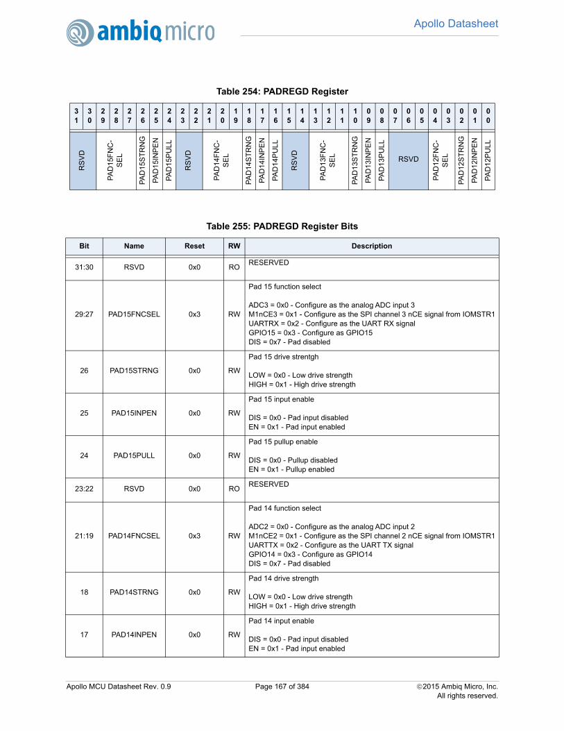
Apollo Datasheet
223
Table 254: PADREGD Register
31
30
29
28
27
26
25
24
23
22
21
20
19
18
17
16
15
14
13
12
11
10
09
08
07
06
05
04
03
02
01
00
RS
VD
PA
D15
FN
C-
SE
L
PA
D15
ST
RN
G
PA
D1
5IN
PE
N
PA
D1
5PU
LL
RS
VD
PA
D14
FN
C-
SE
L
PA
D14
ST
RN
G
PA
D1
4IN
PE
N
PA
D1
4PU
LL
RS
VD
PA
D13
FN
C-
SE
L
PA
D13
ST
RN
G
PA
D1
3IN
PE
N
PA
D1
3PU
LL
RSVD
PA
D12
FN
C-
SE
L
PA
D12
ST
RN
G
PA
D1
2IN
PE
N
PA
D1
2PU
LL
Table 255: PADREGD Register Bits
Bit Name Reset RW Description
31:30 RSVD 0x0 RORESERVED
29:27 PAD15FNCSEL 0x3 RW
Pad 15 function select
ADC3 = 0x0 - Configure as the analog ADC input 3M1nCE3 = 0x1 - Configure as the SPI channel 3 nCE signal from IOMSTR1UARTRX = 0x2 - Configure as the UART RX signalGPIO15 = 0x3 - Configure as GPIO15DIS = 0x7 - Pad disabled
26 PAD15STRNG 0x0 RW
Pad 15 drive strentgh
LOW = 0x0 - Low drive strengthHIGH = 0x1 - High drive strength
25 PAD15INPEN 0x0 RW
Pad 15 input enable
DIS = 0x0 - Pad input disabledEN = 0x1 - Pad input enabled
24 PAD15PULL 0x0 RW
Pad 15 pullup enable
DIS = 0x0 - Pullup disabledEN = 0x1 - Pullup enabled
23:22 RSVD 0x0 RORESERVED
21:19 PAD14FNCSEL 0x3 RW
Pad 14 function select
ADC2 = 0x0 - Configure as the analog ADC input 2M1nCE2 = 0x1 - Configure as the SPI channel 2 nCE signal from IOMSTR1UARTTX = 0x2 - Configure as the UART TX signalGPIO14 = 0x3 - Configure as GPIO14DIS = 0x7 - Pad disabled
18 PAD14STRNG 0x0 RW
Pad 14 drive strength
LOW = 0x0 - Low drive strengthHIGH = 0x1 - High drive strength
17 PAD14INPEN 0x0 RW
Pad 14 input enable
DIS = 0x0 - Pad input disabledEN = 0x1 - Pad input enabled
Apollo MCU Datasheet Rev. 0.9 Page 167 of 384 2015 Ambiq Micro, Inc.All rights reserved.

Apollo Datasheet
223
7.6.2.5 PADREGE Register
Pad Configuration Register E
OFFSET: 0x00000010
INSTANCE 0 ADDRESS: 0x40010010
16 PAD14PULL 0x0 RW
Pad 14 pullup enable
DIS = 0x0 - Pullup disabledEN = 0x1 - Pullup enabled
15:14 RSVD 0x0 RORESERVED
13:11 PAD13FNCSEL 0x3 RW
Pad 13 function select
ADC1 = 0x0 - Configure as the analog ADC input 1M1nCE1 = 0x1 - Configure as the SPI channel 1 nCE signal from IOMSTR1TCTB0 = 0x2 - Configure as the input/output signal from CTIMER B0GPIO13 = 0x3 - Configure as GPIO13SWO = 0x6 - Configure as the serial wire debug SWO signalDIS = 0x7 - Pad disabled
10 PAD13STRNG 0x0 RW
Pad 13 drive strength
LOW = 0x0 - Low drive strengthHIGH = 0x1 - High drive strength
9 PAD13INPEN 0x0 RW
Pad 13 input enable
DIS = 0x0 - Pad input disabledEN = 0x1 - Pad input enabled
8 PAD13PULL 0x0 RW
Pad 13 pullup enable
DIS = 0x0 - Pullup disabledEN = 0x1 - Pullup enabled
7:5 RSVD 0x0 RORESERVED
4:3 PAD12FNCSEL 0x3 RW
Pad 12 function select
ADC0 = 0x0 - Configure as the analog ADC input 0M1nCE0 = 0x1 - Configure as the SPI channel 0 nCE signal from IOMSTR1TCTA0 = 0x2 - Configure as the input/output signal from CTIMER A0GPIO12 = 0x3 - Configure as GPIO12
2 PAD12STRNG 0x0 RW
Pad 12 drive strength
LOW = 0x0 - Low drive strengthHIGH = 0x1 - High drive strength
1 PAD12INPEN 0x0 RW
Pad 12 input enable
DIS = 0x0 - Pad input disabledEN = 0x1 - Pad input enabled
0 PAD12PULL 0x0 RW
Pad 12 pullup enable
DIS = 0x0 - Pullup disabledEN = 0x1 - Pullup enabled
Table 255: PADREGD Register Bits
Bit Name Reset RW Description
Apollo MCU Datasheet Rev. 0.9 Page 168 of 384 2015 Ambiq Micro, Inc.All rights reserved.

Apollo Datasheet
223
This register controls the pad configuration controls for PAD19 through PAD16. Writes to this register mustbe unlocked by the PADKEY register.Table 256: PADREGE Register
31
30
29
28
27
26
25
24
23
22
21
20
19
18
17
16
15
14
13
12
11
10
09
08
07
06
05
04
03
02
01
00
RSVD
PA
D19
FN
C-
SE
L
PA
D19
ST
RN
G
PA
D19
INP
EN
PA
D19
PU
LL
RSVD
PA
D18
FN
C-
SE
L
PA
D18
ST
RN
G
PA
D18
INP
EN
PA
D18
PU
LL
RS
VD
PA
D17
FN
C-
SE
L
PA
D17
ST
RN
G
PA
D17
INP
EN
PA
D17
PU
LL
RSVD
PA
D16
FN
C-
SE
L
PA
D16
ST
RN
G
PA
D16
INP
EN
PA
D16
PU
LL
Table 257: PADREGE Register Bits
Bit Name Reset RW Description
31:29 RSVD 0x0 RORESERVED
28:27 PAD19FNCSEL 0x3 RW
Pad 19 function select
CMPRF = 0x0 - Configure as the analog comparator reference signalM0nCE3 = 0x1 - Configure as the SPI channel 3 nCE signal from IOMSTR0TCTB1 = 0x2 - Configure as the input/output signal from CTIMER B1GPIO19 = 0x3 - Configure as GPIO19
26 PAD19STRNG 0x0 RW
Pad 19 drive strentgh
LOW = 0x0 - Low drive strengthHIGH = 0x1 - High drive strength
25 PAD19INPEN 0x0 RW
Pad 19 input enable
DIS = 0x0 - Pad input disabledEN = 0x1 - Pad input enabled
24 PAD19PULL 0x0 RW
Pad 19 pullup enable
DIS = 0x0 - Pullup disabledEN = 0x1 - Pullup enabled
23:21 RSVD 0x0 RORESERVED
20:19 PAD18FNCSEL 0x3 RW
Pad 18 function select
CMPIN1 = 0x0 - Configure as the analog comparator input 1 signalM0nCE2 = 0x1 - Configure as the SPI channel 2 nCE signal from IOMSTR0TCTA1 = 0x2 - Configure as the input/output signal from CTIMER A1GPIO18 = 0x3 - Configure as GPIO18
18 PAD18STRNG 0x0 RW
Pad 18 drive strength
LOW = 0x0 - Low drive strengthHIGH = 0x1 - High drive strength
Apollo MCU Datasheet Rev. 0.9 Page 169 of 384 2015 Ambiq Micro, Inc.All rights reserved.

Apollo Datasheet
223
17 PAD18INPEN 0x0 RW
Pad 18 input enable
DIS = 0x0 - Pad input disabledEN = 0x1 - Pad input enabled
16 PAD18PULL 0x0 RW
Pad 18 pullup enable
DIS = 0x0 - Pullup disabledEN = 0x1 - Pullup enabled
15:14 RSVD 0x0 RORESERVED
13:11 PAD17FNCSEL 0x3 RW
Pad 17 function select
CMPIN0 = 0x0 - Configure as the analog comparator input 0 signalM0nCE1 = 0x1 - Configure as the SPI channel 1 nCE signal from IOMSTR0TRIG3 = 0x2 - Configure as the ADC Trigger 3 signalGPIO17 = 0x3 - Configure as GPIO17DIS = 0x7 - Pad disabled
10 PAD17STRNG 0x0 RW
Pad 17 drive strength
LOW = 0x0 - Low drive strengthHIGH = 0x1 - High drive strength
9 PAD17INPEN 0x0 RW
Pad 17 input enable
DIS = 0x0 - Pad input disabledEN = 0x1 - Pad input enabled
8 PAD17PULL 0x0 RW
Pad 17 pullup enable
DIS = 0x0 - Pullup disabledEN = 0x1 - Pullup enabled
7:5 RSVD 0x0 RORESERVED
4:3 PAD16FNCSEL 0x3 RW
Pad 16 function select
ADCREF = 0x0 - Configure as the analog ADC reference input signalM0nCE4 = 0x1 - Configure as the SPI channel 4 nCE signal from IOMSTR0TRIG2 = 0x2 - Configure as the ADC Trigger 2 signalGPIO16 = 0x3 - Configure as GPIO16
2 PAD16STRNG 0x0 RW
Pad 16 drive strength
LOW = 0x0 - Low drive strengthHIGH = 0x1 - High drive strength
1 PAD16INPEN 0x0 RW
Pad 16 input enable
DIS = 0x0 - Pad input disabledEN = 0x1 - Pad input enabled
0 PAD16PULL 0x0 RW
Pad 16 pullup enable
DIS = 0x0 - Pullup disabledEN = 0x1 - Pullup enabled
Table 257: PADREGE Register Bits
Bit Name Reset RW Description
Apollo MCU Datasheet Rev. 0.9 Page 170 of 384 2015 Ambiq Micro, Inc.All rights reserved.

Apollo Datasheet
223
7.6.2.6 PADREGF RegisterPad Configuration Register F
OFFSET: 0x00000014
INSTANCE 0 ADDRESS: 0x40010014
This register controls the pad configuration controls for PAD23 through PAD20. Writes to this register mustbe unlocked by the PADKEY register.
Table 258: PADREGF Register
31
30
29
28
27
26
25
24
23
22
21
20
19
18
17
16
15
14
13
12
11
10
09
08
07
06
05
04
03
02
01
00
RSVD
PA
D23
FN
C-
SE
L
PA
D23
ST
RN
G
PA
D23
INP
EN
PA
D23
PU
LL
RSVD
PA
D22
FN
C-
SE
L
PA
D22
ST
RN
G
PA
D22
INP
EN
PA
D22
PU
LL
RSVD
PA
D21
FN
C-
SE
L
PA
D21
ST
RN
G
PA
D21
INP
EN
PA
D21
PU
LL
RSVD
PA
D20
FN
C-
SE
L
PA
D20
ST
RN
G
PA
D20
INP
EN
PA
D20
PU
LL
Table 259: PADREGF Register Bits
Bit Name Reset RW Description
31:29 RSVD 0x0 RORESERVED
28:27 PAD23FNCSEL 0x3 RW
Pad 23 function select
UARTRX = 0x0 - Configure as the UART RX signalM0nCE0 = 0x1 - Configure as the SPI channel 0 nCE signal from IOMSTR0TCTB3 = 0x2 - Configure as the input/output signal from CTIMER B3GPIO23 = 0x3 - Configure as GPIO23
26 PAD23STRNG 0x0 RW
Pad 23 drive strentgh
LOW = 0x0 - Low drive strengthHIGH = 0x1 - High drive strength
25 PAD23INPEN 0x0 RW
Pad 23 input enable
DIS = 0x0 - Pad input disabledEN = 0x1 - Pad input enabled
24 PAD23PULL 0x0 RW
Pad 23 pullup enable
DIS = 0x0 - Pullup disabledEN = 0x1 - Pullup enabled
23:21 RSVD 0x0 RORESERVED
20:19 PAD22FNCSEL 0x3 RW
Pad 22 function select
UARTTX = 0x0 - Configure as the UART TX signalM1nCE7 = 0x1 - Configure as the SPI channel 7 nCE signal from IOMSTR1TCTA3 = 0x2 - Configure as the input/output signal from CTIMER A3GPIO22 = 0x3 - Configure as GPIO22
Apollo MCU Datasheet Rev. 0.9 Page 171 of 384 2015 Ambiq Micro, Inc.All rights reserved.

Apollo Datasheet
223
18 PAD22STRNG 0x0 RW
Pad 22 drive strength
LOW = 0x0 - Low drive strengthHIGH = 0x1 - High drive strength
17 PAD22INPEN 0x0 RW
Pad 22 input enable
DIS = 0x0 - Pad input disabledEN = 0x1 - Pad input enabled
16 PAD22PULL 0x0 RW
Pad 22 pullup enable
DIS = 0x0 - Pullup disabledEN = 0x1 - Pullup enabled
15:13 RSVD 0x0 RORESERVED
12:11 PAD21FNCSEL 0x0 RW
Pad 21 function select
SWDIO = 0x0 - Configure as the serial wire debug data signalM1nCE6 = 0x1 - Configure as the SPI channel 6 nCE signal from IOMSTR1TCTB2 = 0x2 - Configure as the input/output signal from CTIMER B2GPIO21 = 0x3 - Configure as GPIO21
10 PAD21STRNG 0x0 RW
Pad 21 drive strength
LOW = 0x0 - Low drive strengthHIGH = 0x1 - High drive strength
9 PAD21INPEN 0x1 RW
Pad 21 input enable
DIS = 0x0 - Pad input disabledEN = 0x1 - Pad input enabled
8 PAD21PULL 0x0 RW
Pad 21 pullup enable
DIS = 0x0 - Pullup disabledEN = 0x1 - Pullup enabled
7:5 RSVD 0x0 RORESERVED
4:3 PAD20FNCSEL 0x0 RW
Pad 20 function select
SWDCK = 0x0 - Configure as the serial wire debug clock signalM1nCE5 = 0x1 - Configure as the SPI channel 5 nCE signal from IOMSTR1TCTA2 = 0x2 - Configure as the input/output signal from CTIMER A2GPIO20 = 0x3 - Configure as GPIO20
2 PAD20STRNG 0x0 RW
Pad 20 drive strength
LOW = 0x0 - Low drive strengthHIGH = 0x1 - High drive strength
1 PAD20INPEN 0x1 RW
Pad 20 input enable
DIS = 0x0 - Pad input disabledEN = 0x1 - Pad input enabled
0 PAD20PULL 0x0 RW
Pad 20 pulldown enable
DIS = 0x0 - Pulldown disabledEN = 0x1 - Pulldown enabled
Table 259: PADREGF Register Bits
Bit Name Reset RW Description
Apollo MCU Datasheet Rev. 0.9 Page 172 of 384 2015 Ambiq Micro, Inc.All rights reserved.

Apollo Datasheet
223
7.6.2.7 PADREGG RegisterPad Configuration Register G
OFFSET: 0x00000018
INSTANCE 0 ADDRESS: 0x40010018
This register controls the pad configuration controls for PAD27 through PAD24. Writes to this register mustbe unlocked by the PADKEY register.
Table 260: PADREGG Register
31
30
29
28
27
26
25
24
23
22
21
20
19
18
17
16
15
14
13
12
11
10
09
08
07
06
05
04
03
02
01
00
RSVD
PA
D27
FN
C-
SE
L
PA
D27
ST
RN
G
PA
D27
INP
EN
PA
D27
PU
LL
RSVD
PA
D26
FN
C-
SE
L
PA
D26
ST
RN
G
PA
D26
INP
EN
PA
D26
PU
LL
RSVD
PA
D25
FN
C-
SE
L
PA
D25
ST
RN
G
PA
D25
INP
EN
PA
D25
PU
LL
RSVD
PA
D24
FN
C-
SE
L
PA
D24
ST
RN
G
PA
D24
INP
EN
PA
D24
PU
LL
Table 261: PADREGG Register Bits
Bit Name Reset RW Description
31:29 RSVD 0x0 RORESERVED
28:27 PAD27FNCSEL 0x3 RW
Pad 27 function select
M1nCE4 = 0x1 - Configure as the SPI channel 4 nCE signal from IOMSTR1TCTA1 = 0x2 - Configure as the input/output signal from CTIMER A1GPIO27 = 0x3 - Configure as GPIO27
26 PAD27STRNG 0x0 RW
Pad 27 drive strentgh
LOW = 0x0 - Low drive strengthHIGH = 0x1 - High drive strength
25 PAD27INPEN 0x0 RW
Pad 27 input enable
DIS = 0x0 - Pad input disabledEN = 0x1 - Pad input enabled
24 PAD27PULL 0x0 RW
Pad 27 pullup enable
DIS = 0x0 - Pullup disabledEN = 0x1 - Pullup enabled
23:21 RSVD 0x0 RORESERVED
20:19 PAD26FNCSEL 0x3 RW
Pad 26 function select
M0nCE3 = 0x1 - Configure as the SPI channel 3 nCE signal from IOMSTR0TCTB0 = 0x2 - Configure as the input/output signal from CTIMER B0GPIO26 = 0x3 - Configure as GPIO26
Apollo MCU Datasheet Rev. 0.9 Page 173 of 384 2015 Ambiq Micro, Inc.All rights reserved.

Apollo Datasheet
223
18 PAD26STRNG 0x0 RW
Pad 26 drive strength
LOW = 0x0 - Low drive strengthHIGH = 0x1 - High drive strength
17 PAD26INPEN 0x0 RW
Pad 26 input enable
DIS = 0x0 - Pad input disabledEN = 0x1 - Pad input enabled
16 PAD26PULL 0x0 RW
Pad 26 pullup enable
DIS = 0x0 - Pullup disabledEN = 0x1 - Pullup enabled
15:13 RSVD 0x0 RORESERVED
12:11 PAD25FNCSEL 0x3 RW
Pad 25 function select
M0nCE2 = 0x1 - Configure as the SPI channel 2 nCE signal from IOMSTR0TCTA0 = 0x2 - Configure as the input/output signal from CTIMER A0GPIO25 = 0x3 - Configure as GPIO25
10 PAD25STRNG 0x0 RW
Pad 25 drive strength
LOW = 0x0 - Low drive strengthHIGH = 0x1 - High drive strength
9 PAD25INPEN 0x0 RW
Pad 25 input enable
DIS = 0x0 - Pad input disabledEN = 0x1 - Pad input enabled
8 PAD25PULL 0x0 RW
Pad 25 pullup enable
DIS = 0x0 - Pullup disabledEN = 0x1 - Pullup enabled
7:5 RSVD 0x0 RORESERVED
4:3 PAD24FNCSEL 0x3 RW
Pad 24 function select
DIS = 0x0 - Pad disabledM0nCE1 = 0x1 - Configure as the SPI channel 1 nCE signal from IOMSTR0CLKOUT = 0x2 - Configure as the CLKOUT signalGPIO24 = 0x3 - Configure as GPIO24
2 PAD24STRNG 0x0 RW
Pad 24 drive strength
LOW = 0x0 - Low drive strengthHIGH = 0x1 - High drive strength
1 PAD24INPEN 0x0 RW
Pad 24 input enable
DIS = 0x0 - Pad input disabledEN = 0x1 - Pad input enabled
0 PAD24PULL 0x0 RW
Pad 24 pullup enable
DIS = 0x0 - Pullup disabledEN = 0x1 - Pullup enabled
Table 261: PADREGG Register Bits
Bit Name Reset RW Description
Apollo MCU Datasheet Rev. 0.9 Page 174 of 384 2015 Ambiq Micro, Inc.All rights reserved.

Apollo Datasheet
223
7.6.2.8 PADREGH RegisterPad Configuration Register H
OFFSET: 0x0000001C
INSTANCE 0 ADDRESS: 0x4001001C
This register controls the pad configuration controls for PAD31 through PAD28. Writes to this register mustbe unlocked by the PADKEY register.
Table 262: PADREGH Register
31
30
29
28
27
26
25
24
23
22
21
20
19
18
17
16
15
14
13
12
11
10
09
08
07
06
05
04
03
02
01
00
RSVD
PA
D31
FN
C-
SE
L
PA
D31
ST
RN
G
PA
D31
INP
EN
PA
D31
PU
LL
RSVD
PA
D30
FN
C-
SE
L
PA
D30
ST
RN
G
PA
D30
INP
EN
PA
D30
PU
LL
RSVD
PA
D29
FN
C-
SE
L
PA
D29
ST
RN
G
PA
D29
INP
EN
PA
D29
PU
LL
RSVD
PA
D28
FN
C-
SE
L
PA
D28
ST
RN
G
PA
D28
INP
EN
PA
D28
PU
LL
Table 263: PADREGH Register Bits
Bit Name Reset RW Description
31:29 RSVD 0x0 RORESERVED
28:27 PAD31FNCSEL 0x3 RW
Pad 31 function select
ADC6 = 0x0 - Configure as the analog ADC input 6 signalM0nCE4 = 0x1 - Configure as the SPI channel 4 nCE signal from IOMSTR0TCTA3 = 0x2 - Configure as the input/output signal from CTIMER A3GPIO31 = 0x3 - Configure as GPIO31
26 PAD31STRNG 0x0 RW
Pad 31 drive strentgh
LOW = 0x0 - Low drive strengthHIGH = 0x1 - High drive strength
25 PAD31INPEN 0x0 RW
Pad 31 input enable
DIS = 0x0 - Pad input disabledEN = 0x1 - Pad input enabled
24 PAD31PULL 0x0 RW
Pad 31 pullup enable
DIS = 0x0 - Pullup disabledEN = 0x1 - Pullup enabled
23:21 RSVD 0x0 RORESERVED
20:19 PAD30FNCSEL 0x3 RW
Pad 30 function select
ADC5 = 0x0 - Configure as the analog ADC input 5 signalM1nCE7 = 0x1 - Configure as the SPI channel 7 nCE signal from IOMSTR1TCTB2 = 0x2 - Configure as the input/output signal from CTIMER B2GPIO30 = 0x3 - Configure as GPIO30
Apollo MCU Datasheet Rev. 0.9 Page 175 of 384 2015 Ambiq Micro, Inc.All rights reserved.

Apollo Datasheet
223
18 PAD30STRNG 0x0 RW
Pad 30 drive strength
LOW = 0x0 - Low drive strengthHIGH = 0x1 - High drive strength
17 PAD30INPEN 0x0 RW
Pad 30 input enable
DIS = 0x0 - Pad input disabledEN = 0x1 - Pad input enabled
16 PAD30PULL 0x0 RW
Pad 30 pullup enable
DIS = 0x0 - Pullup disabledEN = 0x1 - Pullup enabled
15:13 RSVD 0x0 RORESERVED
12:11 PAD29FNCSEL 0x3 RW
Pad 29 function select
ADC4 = 0x0 - Configure as the analog ADC input 4 signalM1nCE6 = 0x1 - Configure as the SPI channel 6 nCE signal from IOMSTR1TCTA2 = 0x2 - Configure as the input/output signal from CTIMER A2GPIO29 = 0x3 - Configure as GPIO29
10 PAD29STRNG 0x0 RW
Pad 29 drive strength
LOW = 0x0 - Low drive strengthHIGH = 0x1 - High drive strength
9 PAD29INPEN 0x0 RW
Pad 29 input enable
DIS = 0x0 - Pad input disabledEN = 0x1 - Pad input enabled
8 PAD29PULL 0x0 RW
Pad 29 pullup enable
DIS = 0x0 - Pullup disabledEN = 0x1 - Pullup enabled
7:5 RSVD 0x0 RORESERVED
4:3 PAD28FNCSEL 0x3 RW
Pad 28 function select
DIS = 0x0 - Pad disabledM1nCE5 = 0x1 - Configure as the SPI channel 5 nCE signal from IOMSTR1TCTB1 = 0x2 - Configure as the input/output signal from CTIMER B1GPIO28 = 0x3 - Configure as GPIO28
2 PAD28STRNG 0x0 RW
Pad 28 drive strength
LOW = 0x0 - Low drive strengthHIGH = 0x1 - High drive strength
1 PAD28INPEN 0x0 RW
Pad 28 input enable
DIS = 0x0 - Pad input disabledEN = 0x1 - Pad input enabled
0 PAD28PULL 0x0 RW
Pad 28 pullup enable
DIS = 0x0 - Pullup disabledEN = 0x1 - Pullup enabled
Table 263: PADREGH Register Bits
Bit Name Reset RW Description
Apollo MCU Datasheet Rev. 0.9 Page 176 of 384 2015 Ambiq Micro, Inc.All rights reserved.

Apollo Datasheet
223
7.6.2.9 PADREGI RegisterPad Configuration Register I
OFFSET: 0x00000020
INSTANCE 0 ADDRESS: 0x40010020
This register controls the pad configuration controls for PAD35 through PAD32. Writes to this register mustbe unlocked by the PADKEY register.
Table 264: PADREGI Register
31
30
29
28
27
26
25
24
23
22
21
20
19
18
17
16
15
14
13
12
11
10
09
08
07
06
05
04
03
02
01
00
RSVD
PA
D35
FN
C-
SE
L
PA
D35
ST
RN
G
PA
D35
INP
EN
PA
D35
PU
LL
RSVD
PA
D34
FN
C-
SE
L
PA
D34
ST
RN
G
PA
D34
INP
EN
PA
D34
PU
LL
RSVD
PA
D33
FN
C-
SE
L
PA
D33
ST
RN
G
PA
D33
INP
EN
PA
D33
PU
LL
RSVD
PA
D32
FN
C-
SE
L
PA
D32
ST
RN
G
PA
D32
INP
EN
PA
D32
PU
LL
Table 265: PADREGI Register Bits
Bit Name Reset RW Description
31:29 RSVD 0x0 RORESERVED
28:27 PAD35FNCSEL 0x3 RW
Pad 35 function select
DIS = 0x0 - Pad disabledM1nCE0 = 0x1 - Configure as the SPI channel 0 nCE signal from IOMSTR1UARTTX = 0x2 - Configure as the UART TX signalGPIO35 = 0x3 - Configure as GPIO35
26 PAD35STRNG 0x0 RW
Pad 35 drive strentgh
LOW = 0x0 - Low drive strengthHIGH = 0x1 - High drive strength
25 PAD35INPEN 0x0 RW
Pad 35 input enable
DIS = 0x0 - Pad input disabledEN = 0x1 - Pad input enabled
24 PAD35PULL 0x0 RW
Pad 35 pullup enable
DIS = 0x0 - Pullup disabledEN = 0x1 - Pullup enabled
23:21 RSVD 0x0 RORESERVED
20:19 PAD34FNCSEL 0x3 RW
Pad 34 function select
CMPRF2 = 0x0 - Configure as the analog comparator reference 2 signalM0nCE7 = 0x1 - Configure as the SPI channel 7 nCE signal from IOMSTR0DIS = 0x2 - Pad disabledGPIO34 = 0x3 - Configure as GPIO34
Apollo MCU Datasheet Rev. 0.9 Page 177 of 384 2015 Ambiq Micro, Inc.All rights reserved.

Apollo Datasheet
223
18 PAD34STRNG 0x0 RW
Pad 34 drive strength
LOW = 0x0 - Low drive strengthHIGH = 0x1 - High drive strength
17 PAD34INPEN 0x0 RW
Pad 34 input enable
DIS = 0x0 - Pad input disabledEN = 0x1 - Pad input enabled
16 PAD34PULL 0x0 RW
Pad 34 pullup enable
DIS = 0x0 - Pullup disabledEN = 0x1 - Pullup enabled
15:13 RSVD 0x0 RORESERVED
12:11 PAD33FNCSEL 0x3 RW
Pad 33 function select
CMPRF1 = 0x0 - Configure as the analog comparator reference 1 signalM0nCE6 = 0x1 - Configure as the SPI channel 6 nCE signal from IOMSTR0DIS = 0x2 - Pad disabledGPIO33 = 0x3 - Configure as GPIO33
10 PAD33STRNG 0x0 RW
Pad 33 drive strength
LOW = 0x0 - Low drive strengthHIGH = 0x1 - High drive strength
9 PAD33INPEN 0x0 RW
Pad 33 input enable
DIS = 0x0 - Pad input disabledEN = 0x1 - Pad input enabled
8 PAD33PULL 0x0 RW
Pad 33 pullup enable
DIS = 0x0 - Pullup disabledEN = 0x1 - Pullup enabled
7:5 RSVD 0x0 RORESERVED
4:3 PAD32FNCSEL 0x3 RW
Pad 32 function select
ADC7 = 0x0 - Configure as the analog ADC input 7 signalM0nCE5 = 0x1 - Configure as the SPI channel 5 nCE signal from IOMSTR0TCTB3 = 0x2 - Configure as the input/output signal from CTIMER B3GPIO32 = 0x3 - Configure as GPIO32
2 PAD32STRNG 0x0 RW
Pad 32 drive strength
LOW = 0x0 - Low drive strengthHIGH = 0x1 - High drive strength
1 PAD32INPEN 0x0 RW
Pad 32 input enable
DIS = 0x0 - Pad input disabledEN = 0x1 - Pad input enabled
0 PAD32PULL 0x0 RW
Pad 32 pullup enable
DIS = 0x0 - Pullup disabledEN = 0x1 - Pullup enabled
Table 265: PADREGI Register Bits
Bit Name Reset RW Description
Apollo MCU Datasheet Rev. 0.9 Page 178 of 384 2015 Ambiq Micro, Inc.All rights reserved.

Apollo Datasheet
223
7.6.2.10 PADREGJ RegisterPad Configuration Register J
OFFSET: 0x00000024
INSTANCE 0 ADDRESS: 0x40010024
This register controls the pad configuration controls for PAD39 through PAD36. Writes to this register mustbe unlocked by the PADKEY register.
Table 266: PADREGJ Register
31
30
29
28
27
26
25
24
23
22
21
20
19
18
17
16
15
14
13
12
11
10
09
08
07
06
05
04
03
02
01
00
RSVD
PA
D39
FN
C-
SE
L
PA
D39
ST
RN
G
PA
D39
INP
EN
PA
D39
PU
LL
RSVD
PA
D38
FN
C-
SE
L
PA
D38
ST
RN
G
PA
D38
INP
EN
PA
D38
PU
LL
RSVD
PA
D37
FN
C-
SE
L
PA
D37
ST
RN
G
PA
D37
INP
EN
PA
D37
PU
LL
RSVD
PA
D36
FN
C-
SE
L
PA
D36
ST
RN
G
PA
D36
INP
EN
PA
D36
PU
LL
Table 267: PADREGJ Register Bits
Bit Name Reset RW Description
31:29 RSVD 0x0 RORESERVED
28:27 PAD39FNCSEL 0x3 RW
Pad 39 function select
TRIG2 = 0x0 - Configure as the ADC Trigger 2 signalUARTTX = 0x1 - Configure as the UART TX signalCLKOUT = 0x2 - Configure as the CLKOUT signalGPIO39 = 0x3 - Configure as GPIO39
26 PAD39STRNG 0x0 RW
Pad 39 drive strentgh
LOW = 0x0 - Low drive strengthHIGH = 0x1 - High drive strength
25 PAD39INPEN 0x0 RW
Pad 39 input enable
DIS = 0x0 - Pad input disabledEN = 0x1 - Pad input enabled
24 PAD39PULL 0x0 RW
Pad 39 pullup enable
DIS = 0x0 - Pullup disabledEN = 0x1 - Pullup enabled
23:21 RSVD 0x0 RORESERVED
20:19 PAD38FNCSEL 0x3 RW
Pad 38 function select
TRIG1 = 0x0 - Configure as the ADC Trigger 1 signalM1nCE3 = 0x1 - Configure as the SPI channel 3 nCE signal from IOMSTR1UACTS = 0x2 - Configure as the UART CTS signalGPIO38 = 0x3 - Configure as GPIO38
Apollo MCU Datasheet Rev. 0.9 Page 179 of 384 2015 Ambiq Micro, Inc.All rights reserved.

Apollo Datasheet
223
18 PAD38STRNG 0x0 RW
Pad 38 drive strength
LOW = 0x0 - Low drive strengthHIGH = 0x1 - High drive strength
17 PAD38INPEN 0x0 RW
Pad 38 input enable
DIS = 0x0 - Pad input disabledEN = 0x1 - Pad input enabled
16 PAD38PULL 0x0 RW
Pad 38 pullup enable
DIS = 0x0 - Pullup disabledEN = 0x1 - Pullup enabled
15:13 RSVD 0x0 RORESERVED
12:11 PAD37FNCSEL 0x3 RW
Pad 37 function select
TRIG0 = 0x0 - Configure as the ADC Trigger 0 signalM1nCE2 = 0x1 - Configure as the SPI channel 2 nCE signal from IOMSTR1UARTS = 0x2 - Configure as the UART RTS signalGPIO37 = 0x3 - Configure as GPIO37
10 PAD37STRNG 0x0 RW
Pad 37 drive strength
LOW = 0x0 - Low drive strengthHIGH = 0x1 - High drive strength
9 PAD37INPEN 0x0 RW
Pad 37 input enable
DIS = 0x0 - Pad input disabledEN = 0x1 - Pad input enabled
8 PAD37PULL 0x0 RW
Pad 37 pullup enable
DIS = 0x0 - Pullup disabledEN = 0x1 - Pullup enabled
7:5 RSVD 0x0 RORESERVED
4:3 PAD36FNCSEL 0x3 RW
Pad 36 function select
DIS = 0x0 - Pad disabledM1nCE1 = 0x1 - Configure as the SPI channel 1 nCE signal from IOMSTR1UARTRX = 0x2 - Configure as the UART RX signalGPIO36 = 0x3 - Configure as GPIO36
2 PAD36STRNG 0x0 RW
Pad 36 drive strength
LOW = 0x0 - Low drive strengthHIGH = 0x1 - High drive strength
1 PAD36INPEN 0x0 RW
Pad 36 input enable
DIS = 0x0 - Pad input disabledEN = 0x1 - Pad input enabled
0 PAD36PULL 0x0 RW
Pad 36 pullup enable
DIS = 0x0 - Pullup disabledEN = 0x1 - Pullup enabled
Table 267: PADREGJ Register Bits
Bit Name Reset RW Description
Apollo MCU Datasheet Rev. 0.9 Page 180 of 384 2015 Ambiq Micro, Inc.All rights reserved.

Apollo Datasheet
223
7.6.2.11 PADREGK RegisterPad Configuration Register K
OFFSET: 0x00000028
INSTANCE 0 ADDRESS: 0x40010028
This register controls the pad configuration controls for PAD43 through PAD40. Writes to this register mustbe unlocked by the PADKEY register.
Table 268: PADREGK Register
31
30
29
28
27
26
25
24
23
22
21
20
19
18
17
16
15
14
13
12
11
10
09
08
07
06
05
04
03
02
01
00
RSVD
PA
D43
FN
C-
SE
L
PA
D43
ST
RN
G
PA
D43
INP
EN
PA
D43
PU
LL
RSVD
PA
D42
FN
C-
SE
L
PA
D42
ST
RN
G
PA
D42
INP
EN
PA
D42
PU
LL
RSVD
PA
D41
FN
C-
SE
L
PA
D41
ST
RN
G
PA
D41
INP
EN
PA
D41
PU
LL
RSVD
PA
D40
FN
C-
SE
L
PA
D40
ST
RN
G
PA
D40
INP
EN
PA
D40
PU
LL
Table 269: PADREGK Register Bits
Bit Name Reset RW Description
31:29 RSVD 0x0 RORESERVED
28:27 PAD43FNCSEL 0x3 RW
Pad 43 function select
TRIG6 = 0x0 - Configure as the ADC Trigger 6 signalM0nCE1 = 0x1 - Configure as the SPI channel 1 nCE signal from IOMSTR0TCTB0 = 0x2 - Configure as the input/output signal from CTIMER B0GPIO43 = 0x3 - Configure as GPIO43
26 PAD43STRNG 0x0 RW
Pad 43 drive strentgh
LOW = 0x0 - Low drive strengthHIGH = 0x1 - High drive strength
25 PAD43INPEN 0x0 RW
Pad 43 input enable
DIS = 0x0 - Pad input disabledEN = 0x1 - Pad input enabled
24 PAD43PULL 0x0 RW
Pad 43 pullup enable
DIS = 0x0 - Pullup disabledEN = 0x1 - Pullup enabled
23:21 RSVD 0x0 RORESERVED
20:19 PAD42FNCSEL 0x3 RW
Pad 42 function select
TRIG5 = 0x0 - Configure as the ADC Trigger 5 signalM0nCE0 = 0x1 - Configure as the SPI channel 0 nCE signal from IOMSTR0TCTA0 = 0x2 - Configure as the input/output signal from CTIMER A0GPIO42 = 0x3 - Configure as GPIO42
Apollo MCU Datasheet Rev. 0.9 Page 181 of 384 2015 Ambiq Micro, Inc.All rights reserved.

Apollo Datasheet
223
18 PAD42STRNG 0x0 RW
Pad 42 drive strength
LOW = 0x0 - Low drive strengthHIGH = 0x1 - High drive strength
17 PAD42INPEN 0x0 RW
Pad 42 input enable
DIS = 0x0 - Pad input disabledEN = 0x1 - Pad input enabled
16 PAD42PULL 0x0 RW
Pad 42 pullup enable
DIS = 0x0 - Pullup disabledEN = 0x1 - Pullup enabled
15:13 RSVD 0x0 RORESERVED
12:11 PAD41FNCSEL 0x3 RW
Pad 41 function select
TRIG4 = 0x0 - Configure as the ADC Trigger 4 signalDIS = 0x1 - Pad disabledSWO = 0x2 - Configure as the serial wire debug SWO signalGPIO41 = 0x3 - Configure as GPIO41
10 PAD41STRNG 0x0 RW
Pad 41 drive strength
LOW = 0x0 - Low drive strengthHIGH = 0x1 - High drive strength
9 PAD41INPEN 0x0 RW
Pad 41 input enable
DIS = 0x0 - Pad input disabledEN = 0x1 - Pad input enabled
8 PAD41PULL 0x0 RW
Pad 41 pullup enable
DIS = 0x0 - Pullup disabledEN = 0x1 - Pullup enabled
7:5 RSVD 0x0 RORESERVED
4:3 PAD40FNCSEL 0x3 RW
Pad 40 function select
TRIG3 = 0x0 - Configure as the ADC Trigger 3 signalUARTRX = 0x1 - Configure as the UART RX signalDIS = 0x2 - Pad disabledGPIO40 = 0x3 - Configure as GPIO40
2 PAD40STRNG 0x0 RW
Pad 40 drive strength
LOW = 0x0 - Low drive strengthHIGH = 0x1 - High drive strength
1 PAD40INPEN 0x0 RW
Pad 40 input enable
DIS = 0x0 - Pad input disabledEN = 0x1 - Pad input enabled
0 PAD40PULL 0x0 RW
Pad 40 pullup enable
DIS = 0x0 - Pullup disabledEN = 0x1 - Pullup enabled
Table 269: PADREGK Register Bits
Bit Name Reset RW Description
Apollo MCU Datasheet Rev. 0.9 Page 182 of 384 2015 Ambiq Micro, Inc.All rights reserved.

Apollo Datasheet
223
7.6.2.12 PADREGL RegisterPad Configuration Register L
OFFSET: 0x0000002C
INSTANCE 0 ADDRESS: 0x4001002C
This register controls the pad configuration controls for PAD47 through PAD44. Writes to this register mustbe unlocked by the PADKEY register.
Table 270: PADREGL Register
31
30
29
28
27
26
25
24
23
22
21
20
19
18
17
16
15
14
13
12
11
10
09
08
07
06
05
04
03
02
01
00
RSVD
PA
D47
FN
C-
SE
L
PA
D47
ST
RN
G
PA
D47
INP
EN
PA
D47
PU
LL
RSVD
PA
D46
FN
C-
SE
L
PA
D46
ST
RN
G
PA
D46
INP
EN
PA
D46
PU
LL
RSVD
PA
D45
FN
C-
SE
L
PA
D45
ST
RN
G
PA
D45
INP
EN
PA
D45
PU
LL
RSVD
PA
D44
FN
C-
SE
L
PA
D44
ST
RN
G
PA
D44
INP
EN
PA
D44
PU
LL
Table 271: PADREGL Register Bits
Bit Name Reset RW Description
31:29 RSVD 0x0 RORESERVED
28:27 PAD47FNCSEL 0x3 RW
Pad 47 function select
DIS = 0x0 - Pad disabledM0nCE5 = 0x1 - Configure as the SPI channel 5 nCE signal from IOMSTR0TCTB2 = 0x2 - Configure as the input/output signal from CTIMER B2GPIO47 = 0x3 - Configure as GPIO47
26 PAD47STRNG 0x0 RW
Pad 47 drive strentgh
LOW = 0x0 - Low drive strengthHIGH = 0x1 - High drive strength
25 PAD47INPEN 0x0 RW
Pad 47 input enable
DIS = 0x0 - Pad input disabledEN = 0x1 - Pad input enabled
24 PAD47PULL 0x0 RW
Pad 47 pullup enable
DIS = 0x0 - Pullup disabledEN = 0x1 - Pullup enabled
23:21 RSVD 0x0 RORESERVED
20:19 PAD46FNCSEL 0x3 RW
Pad 46 function select
DIS = 0x0 - Pad disabledM0nCE4 = 0x1 - Configure as the SPI channel 4 nCE signal from IOMSTR0TCTA2 = 0x2 - Configure as the input/output signal from CTIMER A2GPIO46 = 0x3 - Configure as GPIO46
Apollo MCU Datasheet Rev. 0.9 Page 183 of 384 2015 Ambiq Micro, Inc.All rights reserved.

Apollo Datasheet
223
18 PAD46STRNG 0x0 RW
Pad 46 drive strength
LOW = 0x0 - Low drive strengthHIGH = 0x1 - High drive strength
17 PAD46INPEN 0x0 RW
Pad 46 input enable
DIS = 0x0 - Pad input disabledEN = 0x1 - Pad input enabled
16 PAD46PULL 0x0 RW
Pad 46 pullup enable
DIS = 0x0 - Pullup disabledEN = 0x1 - Pullup enabled
15:13 RSVD 0x0 RORESERVED
12:11 PAD45FNCSEL 0x3 RW
Pad 45 function select
DIS = 0x0 - Pad disabledM0nCE3 = 0x1 - Configure as the SPI channel 3 nCE signal from IOMSTR0TCTB1 = 0x2 - Configure as the input/output signal from CTIMER B1GPIO45 = 0x3 - Configure as GPIO45
10 PAD45STRNG 0x0 RW
Pad 45 drive strength
LOW = 0x0 - Low drive strengthHIGH = 0x1 - High drive strength
9 PAD45INPEN 0x0 RW
Pad 45 input enable
DIS = 0x0 - Pad input disabledEN = 0x1 - Pad input enabled
8 PAD45PULL 0x0 RW
Pad 45 pullup enable
DIS = 0x0 - Pullup disabledEN = 0x1 - Pullup enabled
7:5 RSVD 0x0 RORESERVED
4:3 PAD44FNCSEL 0x3 RW
Pad 44 function select
TRIG7 = 0x0 - Configure as the ADC Trigger 7 signalM0nCE2 = 0x1 - Configure as the SPI channel 2 nCE signal from IOMSTR0TCTA1 = 0x2 - Configure as the input/output signal from CTIMER A1GPIO44 = 0x3 - Configure as GPIO44
2 PAD44STRNG 0x0 RW
Pad 44 drive strength
LOW = 0x0 - Low drive strengthHIGH = 0x1 - High drive strength
1 PAD44INPEN 0x0 RW
Pad 44 input enable
DIS = 0x0 - Pad input disabledEN = 0x1 - Pad input enabled
0 PAD44PULL 0x0 RW
Pad 44 pullup enable
DIS = 0x0 - Pullup disabledEN = 0x1 - Pullup enabled
Table 271: PADREGL Register Bits
Bit Name Reset RW Description
Apollo MCU Datasheet Rev. 0.9 Page 184 of 384 2015 Ambiq Micro, Inc.All rights reserved.

Apollo Datasheet
223
7.6.2.13 PADREGM RegisterPad Configuration Register M
OFFSET: 0x00000030
INSTANCE 0 ADDRESS: 0x40010030
This register controls the pad configuration controls for PAD49 through PAD48. Writes to this register mustbe unlocked by the PADKEY register.
Table 272: PADREGM Register
31
30
29
28
27
26
25
24
23
22
21
20
19
18
17
16
15
14
13
12
11
10
09
08
07
06
05
04
03
02
01
00
RSVD
PA
D49
FN
C-
SE
L
PA
D49
ST
RN
G
PA
D49
INP
EN
PA
D49
PU
LL
RSVD
PA
D48
FN
C-
SE
L
PA
D48
ST
RN
G
PA
D48
INP
EN
PA
D48
PU
LL
Table 273: PADREGM Register Bits
Bit Name Reset RW Description
31:13 RSVD 0x0 RORESERVED
12:11 PAD49FNCSEL 0x3 RW
Pad 49 function select
DIS = 0x0 - Pad disabledM0nCE7 = 0x1 - Configure as the SPI channel 7 nCE signal from IOMSTR0TCTB3 = 0x2 - Configure as the input/output signal from CTIMER B3GPIO49 = 0x3 - Configure as GPIO49
10 PAD49STRNG 0x0 RW
Pad 49 drive strength
LOW = 0x0 - Low drive strengthHIGH = 0x1 - High drive strength
9 PAD49INPEN 0x0 RW
Pad 49 input enable
DIS = 0x0 - Pad input disabledEN = 0x1 - Pad input enabled
8 PAD49PULL 0x0 RW
Pad 49 pullup enable
DIS = 0x0 - Pullup disabledEN = 0x1 - Pullup enabled
7:5 RSVD 0x0 RORESERVED
4:3 PAD48FNCSEL 0x3 RW
Pad 48 function select
DIS = 0x0 - Pad disabledM0nCE6 = 0x1 - Configure as the SPI channel 6 nCE signal from IOMSTR0TCTA3 = 0x2 - Configure as the input/output signal from CTIMER A3GPIO48 = 0x3 - Configure as GPIO48
Apollo MCU Datasheet Rev. 0.9 Page 185 of 384 2015 Ambiq Micro, Inc.All rights reserved.

Apollo Datasheet
223
7.6.2.14 CFGA Register
GPIO Configuration Register A
OFFSET: 0x00000040
INSTANCE 0 ADDRESS: 0x40010040
GPIO configuration controls for GPIO[7:0]. Writes to this register must be unlocked by the PADKEYregister.
2 PAD48STRNG 0x0 RW
Pad 48 drive strength
LOW = 0x0 - Low drive strengthHIGH = 0x1 - High drive strength
1 PAD48INPEN 0x0 RW
Pad 48 input enable
DIS = 0x0 - Pad input disabledEN = 0x1 - Pad input enabled
0 PAD48PULL 0x0 RW
Pad 48 pullup enable
DIS = 0x0 - Pullup disabledEN = 0x1 - Pullup enabled
Table 274: CFGA Register
31
30
29
28
27
26
25
24
23
22
21
20
19
18
17
16
15
14
13
12
11
10
09
08
07
06
05
04
03
02
01
00
GP
IO7I
NT
D
GP
IO7O
UT
CF
G
GP
IO7I
NC
FG
GP
IO6I
NT
D
GP
IO6O
UT
CF
G
GP
IO6I
NC
FG
GP
IO5I
NT
D
GP
IO5O
UT
CF
G
GP
IO5I
NC
FG
GP
IO4I
NT
D
GP
IO4O
UT
CF
G
GP
IO4I
NC
FG
GP
IO3I
NT
D
GP
IO3O
UT
CF
G
GP
IO3I
NC
FG
GP
IO2I
NT
D
GP
IO2O
UT
CF
G
GP
IO2I
NC
FG
GP
IO1I
NT
D
GP
IO1O
UT
CF
G
GP
IO1I
NC
FG
GP
IO0I
NT
D
GP
IO0O
UT
CF
G
GP
IO0I
NC
FG
Table 275: CFGA Register Bits
Bit Name Reset RW Description
31 GPIO7INTD 0x0 RW
GPIO7 interrupt direction.
INTLH = 0x0 - Interrupt on low to high GPIO transitionINTHL = 0x1 - Interrupt on high to low GPIO transition
30:29 GPIO7OUTCFG 0x0 RW
GPIO7 output configuration.
DIS = 0x0 - Output disabledPUSHPULL = 0x1 - Output is push-pullOD = 0x2 - Output is open drainTS = 0x3 - Output is tri-state
Table 273: PADREGM Register Bits
Bit Name Reset RW Description
Apollo MCU Datasheet Rev. 0.9 Page 186 of 384 2015 Ambiq Micro, Inc.All rights reserved.

Apollo Datasheet
223
28 GPIO7INCFG 0x0 RW
GPIO7 input enable.
READ = 0x0 - Read the GPIO pin dataRDZERO = 0x1 - Readback will always be zero
27 GPIO6INTD 0x0 RW
GPIO6 interrupt direction.
INTLH = 0x0 - Interrupt on low to high GPIO transitionINTHL = 0x1 - Interrupt on high to low GPIO transition
26:25 GPIO6OUTCFG 0x0 RW
GPIO6 output configuration.
DIS = 0x0 - Output disabledPUSHPULL = 0x1 - Output is push-pullOD = 0x2 - Output is open drainTS = 0x3 - Output is tri-state
24 GPIO6INCFG 0x0 RW
GPIO6 input enable.
READ = 0x0 - Read the GPIO pin dataRDZERO = 0x1 - Readback will always be zero
23 GPIO5INTD 0x0 RW
GPIO5 interrupt direction.
INTLH = 0x0 - Interrupt on low to high GPIO transitionINTHL = 0x1 - Interrupt on high to low GPIO transition
22:21 GPIO5OUTCFG 0x0 RW
GPIO5 output configuration.
DIS = 0x0 - Output disabledPUSHPULL = 0x1 - Output is push-pullOD = 0x2 - Output is open drainTS = 0x3 - Output is tri-state
20 GPIO5INCFG 0x0 RW
GPIO5 input enable.
READ = 0x0 - Read the GPIO pin dataRDZERO = 0x1 - Readback will always be zero
19 GPIO4INTD 0x0 RW
GPIO4 interrupt direction.
INTLH = 0x0 - Interrupt on low to high GPIO transitionINTHL = 0x1 - Interrupt on high to low GPIO transition
18:17 GPIO4OUTCFG 0x0 RW
GPIO4 output configuration.
DIS = 0x0 - Output disabledPUSHPULL = 0x1 - Output is push-pullOD = 0x2 - Output is open drainTS = 0x3 - Output is tri-state
16 GPIO4INCFG 0x0 RW
GPIO4 input enable.
READ = 0x0 - Read the GPIO pin dataRDZERO = 0x1 - Readback will always be zero
15 GPIO3INTD 0x0 RW
GPIO3 interrupt direction.
INTLH = 0x0 - Interrupt on low to high GPIO transitionINTHL = 0x1 - Interrupt on high to low GPIO transition
Table 275: CFGA Register Bits
Bit Name Reset RW Description
Apollo MCU Datasheet Rev. 0.9 Page 187 of 384 2015 Ambiq Micro, Inc.All rights reserved.

Apollo Datasheet
223
14:13 GPIO3OUTCFG 0x0 RW
GPIO3 output configuration.
DIS = 0x0 - Output disabledPUSHPULL = 0x1 - Output is push-pullOD = 0x2 - Output is open drainTS = 0x3 - Output is tri-state
12 GPIO3INCFG 0x0 RW
GPIO3 input enable.
READ = 0x0 - Read the GPIO pin dataRDZERO = 0x1 - Readback will always be zero
11 GPIO2INTD 0x0 RW
GPIO2 interrupt direction.
INTLH = 0x0 - Interrupt on low to high GPIO transitionINTHL = 0x1 - Interrupt on high to low GPIO transition
10:9 GPIO2OUTCFG 0x0 RW
GPIO2 output configuration.
DIS = 0x0 - Output disabledPUSHPULL = 0x1 - Output is push-pullOD = 0x2 - Output is open drainTS = 0x3 - Output is tri-state
8 GPIO2INCFG 0x0 RW
GPIO2 input enable.
READ = 0x0 - Read the GPIO pin dataRDZERO = 0x1 - Readback will always be zero
7 GPIO1INTD 0x0 RW
GPIO1 interrupt direction.
INTLH = 0x0 - Interrupt on low to high GPIO transitionINTHL = 0x1 - Interrupt on high to low GPIO transition
6:5 GPIO1OUTCFG 0x0 RW
GPIO1 output configuration.
DIS = 0x0 - Output disabledPUSHPULL = 0x1 - Output is push-pullOD = 0x2 - Output is open drainTS = 0x3 - Output is tri-state
4 GPIO1INCFG 0x0 RW
GPIO1 input enable.
READ = 0x0 - Read the GPIO pin dataRDZERO = 0x1 - Readback will always be zero
3 GPIO0INTD 0x0 RW
GPIO0 interrupt direction.
INTLH = 0x0 - Interrupt on low to high GPIO transitionINTHL = 0x1 - Interrupt on high to low GPIO transition
2:1 GPIO0OUTCFG 0x0 RW
GPIO0 output configuration.
DIS = 0x0 - Output disabledPUSHPULL = 0x1 - Output is push-pullOD = 0x2 - Output is open drainTS = 0x3 - Output is tri-state
0 GPIO0INCFG 0x0 RW
GPIO0 input enable.
READ = 0x0 - Read the GPIO pin dataRDZERO = 0x1 - Readback will always be zero
Table 275: CFGA Register Bits
Bit Name Reset RW Description
Apollo MCU Datasheet Rev. 0.9 Page 188 of 384 2015 Ambiq Micro, Inc.All rights reserved.

Apollo Datasheet
223
7.6.2.15 CFGB RegisterGPIO Configuration Register B
OFFSET: 0x00000044
INSTANCE 0 ADDRESS: 0x40010044
GPIO configuration controls for GPIO[15:8]. Writes to this register must be unlocked by the PADKEYregister.
Table 276: CFGB Register
31
30
29
28
27
26
25
24
23
22
21
20
19
18
17
16
15
14
13
12
11
10
09
08
07
06
05
04
03
02
01
00
GP
IO15
INT
D
GP
IO15
OU
TC
FG
GP
IO15
INC
FG
GP
IO14
INT
D
GP
IO14
OU
TC
FG
GP
IO14
INC
FG
GP
IO13
INT
D
GP
IO13
OU
TC
FG
GP
IO13
INC
FG
GP
IO12
INT
D
GP
IO12
OU
TC
FG
GP
IO12
INC
FG
GP
IO11
INT
D
GP
IO11
OU
TC
FG
GP
IO11
INC
FG
GP
IO10
INT
D
GP
IO10
OU
TC
FG
GP
IO10
INC
FG
GP
IO9I
NT
D
GP
IO9
OU
TC
FG
GP
IO9I
NC
FG
GP
IO8I
NT
D
GP
IO8
OU
TC
FG
GP
IO8I
NC
FG
Table 277: CFGB Register Bits
Bit Name Reset RW Description
31 GPIO15INTD 0x0 RW
GPIO15 interrupt direction.
INTLH = 0x0 - Interrupt on low to high GPIO transitionINTHL = 0x1 - Interrupt on high to low GPIO transition
30:29GPIO15OUT-
CFG0x0 RW
GPIO15 output configuration.
DIS = 0x0 - Output disabledPUSHPULL = 0x1 - Output is push-pullOD = 0x2 - Output is open drainTS = 0x3 - Output is tri-state
28 GPIO15INCFG 0x0 RW
GPIO15 input enable.
READ = 0x0 - Read the GPIO pin dataRDZERO = 0x1 - Readback will always be zero
27 GPIO14INTD 0x0 RW
GPIO14 interrupt direction.
INTLH = 0x0 - Interrupt on low to high GPIO transitionINTHL = 0x1 - Interrupt on high to low GPIO transition
26:25GPIO14OUT-
CFG0x0 RW
GPIO14 output configuration.
DIS = 0x0 - Output disabledPUSHPULL = 0x1 - Output is push-pullOD = 0x2 - Output is open drainTS = 0x3 - Output is tri-state
24 GPIO14INCFG 0x0 RW
GPIO14 input enable.
READ = 0x0 - Read the GPIO pin dataRDZERO = 0x1 - Readback will always be zero
Apollo MCU Datasheet Rev. 0.9 Page 189 of 384 2015 Ambiq Micro, Inc.All rights reserved.

Apollo Datasheet
223
23 GPIO13INTD 0x0 RW
GPIO13 interrupt direction.
INTLH = 0x0 - Interrupt on low to high GPIO transitionINTHL = 0x1 - Interrupt on high to low GPIO transition
22:21GPIO13OUT-
CFG0x0 RW
GPIO13 output configuration.
DIS = 0x0 - Output disabledPUSHPULL = 0x1 - Output is push-pullOD = 0x2 - Output is open drainTS = 0x3 - Output is tri-state
20 GPIO13INCFG 0x0 RW
GPIO13 input enable.
READ = 0x0 - Read the GPIO pin dataRDZERO = 0x1 - Readback will always be zero
19 GPIO12INTD 0x0 RW
GPIO12 interrupt direction.
INTLH = 0x0 - Interrupt on low to high GPIO transitionINTHL = 0x1 - Interrupt on high to low GPIO transition
18:17GPIO12OUT-
CFG0x0 RW
GPIO12 output configuration.
DIS = 0x0 - Output disabledPUSHPULL = 0x1 - Output is push-pullOD = 0x2 - Output is open drainTS = 0x3 - Output is tri-state
16 GPIO12INCFG 0x0 RW
GPIO12 input enable.
READ = 0x0 - Read the GPIO pin dataRDZERO = 0x1 - Readback will always be zero
15 GPIO11INTD 0x0 RW
GPIO11 interrupt direction.
INTLH = 0x0 - Interrupt on low to high GPIO transitionINTHL = 0x1 - Interrupt on high to low GPIO transition
14:13GPIO11OUT-
CFG0x0 RW
GPIO11 output configuration.
DIS = 0x0 - Output disabledPUSHPULL = 0x1 - Output is push-pullOD = 0x2 - Output is open drainTS = 0x3 - Output is tri-state
12 GPIO11INCFG 0x0 RW
GPIO11 input enable.
READ = 0x0 - Read the GPIO pin dataRDZERO = 0x1 - Readback will always be zero
11 GPIO10INTD 0x0 RW
GPIO10 interrupt direction.
INTLH = 0x0 - Interrupt on low to high GPIO transitionINTHL = 0x1 - Interrupt on high to low GPIO transition
10:9GPIO10OUT-
CFG0x0 RW
GPIO10 output configuration.
DIS = 0x0 - Output disabledPUSHPULL = 0x1 - Output is push-pullOD = 0x2 - Output is open drainTS = 0x3 - Output is tri-state
Table 277: CFGB Register Bits
Bit Name Reset RW Description
Apollo MCU Datasheet Rev. 0.9 Page 190 of 384 2015 Ambiq Micro, Inc.All rights reserved.

Apollo Datasheet
223
7.6.2.16 CFGC Register
GPIO Configuration Register C
OFFSET: 0x00000048
INSTANCE 0 ADDRESS: 0x40010048
GPIO configuration controls for GPIO[23:16]. Writes to this register must be unlocked by the PADKEYregister.
8 GPIO10INCFG 0x0 RW
GPIO10 input enable.
READ = 0x0 - Read the GPIO pin dataRDZERO = 0x1 - Readback will always be zero
7 GPIO9INTD 0x0 RW
GPIO9 interrupt direction.
INTLH = 0x0 - Interrupt on low to high GPIO transitionINTHL = 0x1 - Interrupt on high to low GPIO transition
6:5 GPIO9OUTCFG 0x0 RW
GPIO9 output configuration.
DIS = 0x0 - Output disabledPUSHPULL = 0x1 - Output is push-pullOD = 0x2 - Output is open drainTS = 0x3 - Output is tri-state
4 GPIO9INCFG 0x0 RW
GPIO9 input enable.
READ = 0x0 - Read the GPIO pin dataRDZERO = 0x1 - Readback will always be zero
3 GPIO8INTD 0x0 RW
GPIO8 interrupt direction.
INTLH = 0x0 - Interrupt on low to high GPIO transitionINTHL = 0x1 - Interrupt on high to low GPIO transition
2:1 GPIO8OUTCFG 0x0 RW
GPIO8 output configuration.
DIS = 0x0 - Output disabledPUSHPULL = 0x1 - Output is push-pullOD = 0x2 - Output is open drainTS = 0x3 - Output is tri-state
0 GPIO8INCFG 0x0 RW
GPIO8 input enable.
READ = 0x0 - Read the GPIO pin dataRDZERO = 0x1 - Readback will always be zero
Table 277: CFGB Register Bits
Bit Name Reset RW Description
Apollo MCU Datasheet Rev. 0.9 Page 191 of 384 2015 Ambiq Micro, Inc.All rights reserved.
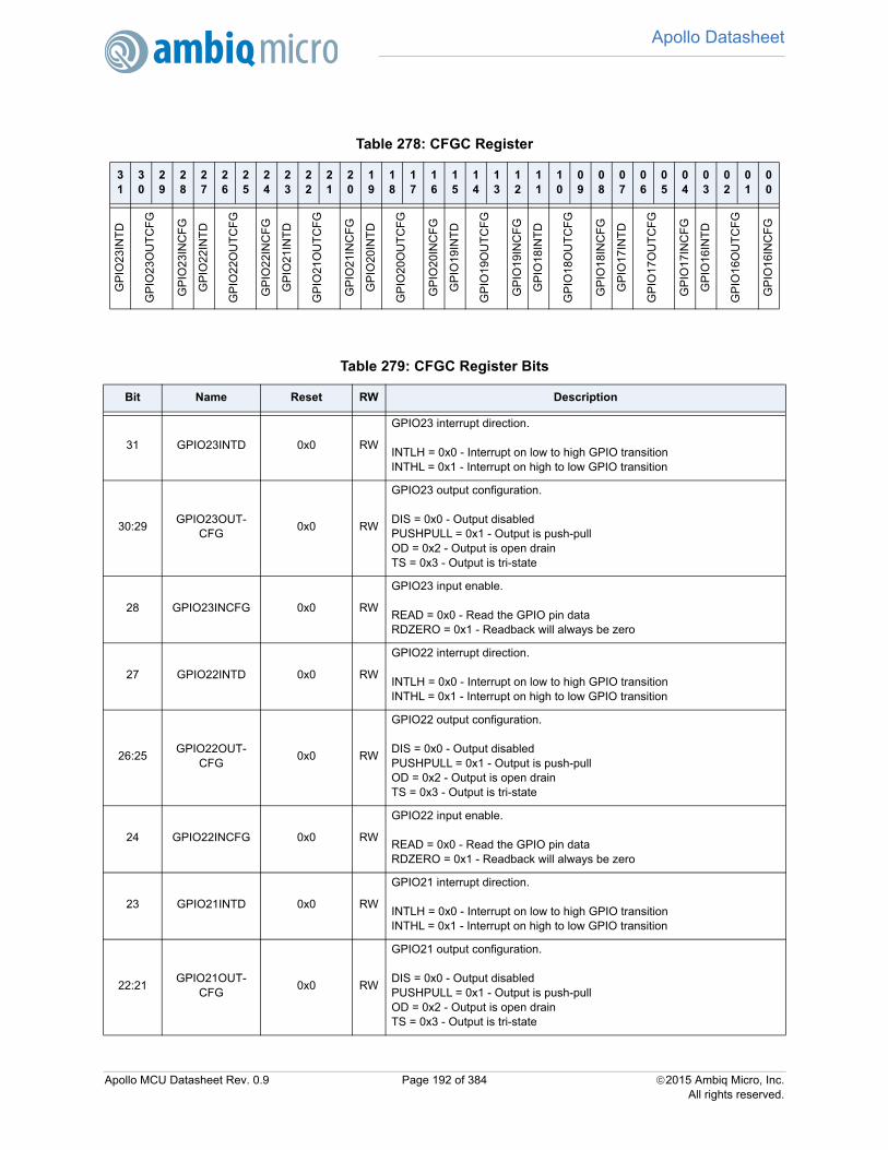
Apollo Datasheet
223
Table 278: CFGC Register
31
30
29
28
27
26
25
24
23
22
21
20
19
18
17
16
15
14
13
12
11
10
09
08
07
06
05
04
03
02
01
00
GP
IO23
INT
D
GP
IO23
OU
TC
FG
GP
IO23
INC
FG
GP
IO22
INT
D
GP
IO22
OU
TC
FG
GP
IO22
INC
FG
GP
IO21
INT
D
GP
IO21
OU
TC
FG
GP
IO21
INC
FG
GP
IO20
INT
D
GP
IO20
OU
TC
FG
GP
IO20
INC
FG
GP
IO19
INT
D
GP
IO19
OU
TC
FG
GP
IO19
INC
FG
GP
IO18
INT
D
GP
IO18
OU
TC
FG
GP
IO18
INC
FG
GP
IO17
INT
D
GP
IO17
OU
TC
FG
GP
IO17
INC
FG
GP
IO16
INT
D
GP
IO16
OU
TC
FG
GP
IO16
INC
FG
Table 279: CFGC Register Bits
Bit Name Reset RW Description
31 GPIO23INTD 0x0 RW
GPIO23 interrupt direction.
INTLH = 0x0 - Interrupt on low to high GPIO transitionINTHL = 0x1 - Interrupt on high to low GPIO transition
30:29GPIO23OUT-
CFG0x0 RW
GPIO23 output configuration.
DIS = 0x0 - Output disabledPUSHPULL = 0x1 - Output is push-pullOD = 0x2 - Output is open drainTS = 0x3 - Output is tri-state
28 GPIO23INCFG 0x0 RW
GPIO23 input enable.
READ = 0x0 - Read the GPIO pin dataRDZERO = 0x1 - Readback will always be zero
27 GPIO22INTD 0x0 RW
GPIO22 interrupt direction.
INTLH = 0x0 - Interrupt on low to high GPIO transitionINTHL = 0x1 - Interrupt on high to low GPIO transition
26:25GPIO22OUT-
CFG0x0 RW
GPIO22 output configuration.
DIS = 0x0 - Output disabledPUSHPULL = 0x1 - Output is push-pullOD = 0x2 - Output is open drainTS = 0x3 - Output is tri-state
24 GPIO22INCFG 0x0 RW
GPIO22 input enable.
READ = 0x0 - Read the GPIO pin dataRDZERO = 0x1 - Readback will always be zero
23 GPIO21INTD 0x0 RW
GPIO21 interrupt direction.
INTLH = 0x0 - Interrupt on low to high GPIO transitionINTHL = 0x1 - Interrupt on high to low GPIO transition
22:21GPIO21OUT-
CFG0x0 RW
GPIO21 output configuration.
DIS = 0x0 - Output disabledPUSHPULL = 0x1 - Output is push-pullOD = 0x2 - Output is open drainTS = 0x3 - Output is tri-state
Apollo MCU Datasheet Rev. 0.9 Page 192 of 384 2015 Ambiq Micro, Inc.All rights reserved.

Apollo Datasheet
223
20 GPIO21INCFG 0x1 RW
GPIO21 input enable.
READ = 0x0 - Read the GPIO pin dataRDZERO = 0x1 - Readback will always be zero
19 GPIO20INTD 0x0 RW
GPIO20 interrupt direction.
INTLH = 0x0 - Interrupt on low to high GPIO transitionINTHL = 0x1 - Interrupt on high to low GPIO transition
18:17GPIO20OUT-
CFG0x0 RW
GPIO20 output configuration.
DIS = 0x0 - Output disabledPUSHPULL = 0x1 - Output is push-pullOD = 0x2 - Output is open drainTS = 0x3 - Output is tri-state
16 GPIO20INCFG 0x1 RW
GPIO20 input enable.
READ = 0x0 - Read the GPIO pin dataRDZERO = 0x1 - Readback will always be zero
15 GPIO19INTD 0x0 RW
GPIO19 interrupt direction.
INTLH = 0x0 - Interrupt on low to high GPIO transitionINTHL = 0x1 - Interrupt on high to low GPIO transition
14:13GPIO19OUT-
CFG0x0 RW
GPIO19 output configuration.
DIS = 0x0 - Output disabledPUSHPULL = 0x1 - Output is push-pullOD = 0x2 - Output is open drainTS = 0x3 - Output is tri-state
12 GPIO19INCFG 0x0 RW
GPIO19 input enable.
READ = 0x0 - Read the GPIO pin dataRDZERO = 0x1 - Readback will always be zero
11 GPIO18INTD 0x0 RW
GPIO18 interrupt direction.
INTLH = 0x0 - Interrupt on low to high GPIO transitionINTHL = 0x1 - Interrupt on high to low GPIO transition
10:9GPIO18OUT-
CFG0x0 RW
GPIO18 output configuration.
DIS = 0x0 - Output disabledPUSHPULL = 0x1 - Output is push-pullOD = 0x2 - Output is open drainTS = 0x3 - Output is tri-state
8 GPIO18INCFG 0x0 RW
GPIO18 input enable.
READ = 0x0 - Read the GPIO pin dataRDZERO = 0x1 - Readback will always be zero
7 GPIO17INTD 0x0 RW
GPIO17 interrupt direction.
INTLH = 0x0 - Interrupt on low to high GPIO transitionINTHL = 0x1 - Interrupt on high to low GPIO transition
Table 279: CFGC Register Bits
Bit Name Reset RW Description
Apollo MCU Datasheet Rev. 0.9 Page 193 of 384 2015 Ambiq Micro, Inc.All rights reserved.

Apollo Datasheet
223
7.6.2.17 CFGD Register
GPIO Configuration Register D
OFFSET: 0x0000004C
INSTANCE 0 ADDRESS: 0x4001004C
GPIO configuration controls for GPIO[31:24]. Writes to this register must be unlocked by the PADKEYregister.
6:5GPIO17OUT-
CFG0x0 RW
GPIO17 output configuration.
DIS = 0x0 - Output disabledPUSHPULL = 0x1 - Output is push-pullOD = 0x2 - Output is open drainTS = 0x3 - Output is tri-state
4 GPIO17INCFG 0x0 RW
GPIO17 input enable.
READ = 0x0 - Read the GPIO pin dataRDZERO = 0x1 - Readback will always be zero
3 GPIO16INTD 0x0 RW
GPIO16 interrupt direction.
INTLH = 0x0 - Interrupt on low to high GPIO transitionINTHL = 0x1 - Interrupt on high to low GPIO transition
2:1GPIO16OUT-
CFG0x0 RW
GPIO16 output configuration.
DIS = 0x0 - Output disabledPUSHPULL = 0x1 - Output is push-pullOD = 0x2 - Output is open drainTS = 0x3 - Output is tri-state
0 GPIO16INCFG 0x0 RW
GPIO16 input enable.
READ = 0x0 - Read the GPIO pin dataRDZERO = 0x1 - Readback will always be zero
Table 280: CFGD Register
31
30
29
28
27
26
25
24
23
22
21
20
19
18
17
16
15
14
13
12
11
10
09
08
07
06
05
04
03
02
01
00
GP
IO31
INT
D
GP
IO31
OU
TC
FG
GP
IO31
INC
FG
GP
IO30
INT
D
GP
IO30
OU
TC
FG
GP
IO30
INC
FG
GP
IO29
INT
D
GP
IO29
OU
TC
FG
GP
IO29
INC
FG
GP
IO28
INT
D
GP
IO28
OU
TC
FG
GP
IO28
INC
FG
GP
IO27
INT
D
GP
IO27
OU
TC
FG
GP
IO27
INC
FG
GP
IO26
INT
D
GP
IO26
OU
TC
FG
GP
IO26
INC
FG
GP
IO25
INT
D
GP
IO25
OU
TC
FG
GP
IO25
INC
FG
GP
IO24
INT
D
GP
IO24
OU
TC
FG
GP
IO24
INC
FG
Table 279: CFGC Register Bits
Bit Name Reset RW Description
Apollo MCU Datasheet Rev. 0.9 Page 194 of 384 2015 Ambiq Micro, Inc.All rights reserved.

Apollo Datasheet
223
Table 281: CFGD Register Bits
Bit Name Reset RW Description
31 GPIO31INTD 0x0 RW
GPIO31 interrupt direction.
INTLH = 0x0 - Interrupt on low to high GPIO transitionINTHL = 0x1 - Interrupt on high to low GPIO transition
30:29GPIO31OUT-
CFG0x0 RW
GPIO31 output configuration.
DIS = 0x0 - Output disabledPUSHPULL = 0x1 - Output is push-pullOD = 0x2 - Output is open drainTS = 0x3 - Output is tri-state
28 GPIO31INCFG 0x0 RW
GPIO31 input enable.
READ = 0x0 - Read the GPIO pin dataRDZERO = 0x1 - Readback will always be zero
27 GPIO30INTD 0x0 RW
GPIO30 interrupt direction.
INTLH = 0x0 - Interrupt on low to high GPIO transitionINTHL = 0x1 - Interrupt on high to low GPIO transition
26:25GPIO30OUT-
CFG0x0 RW
GPIO30 output configuration.
DIS = 0x0 - Output disabledPUSHPULL = 0x1 - Output is push-pullOD = 0x2 - Output is open drainTS = 0x3 - Output is tri-state
24 GPIO30INCFG 0x0 RW
GPIO30 input enable.
READ = 0x0 - Read the GPIO pin dataRDZERO = 0x1 - Readback will always be zero
23 GPIO29INTD 0x0 RW
GPIO29 interrupt direction.
INTLH = 0x0 - Interrupt on low to high GPIO transitionINTHL = 0x1 - Interrupt on high to low GPIO transition
22:21GPIO29OUT-
CFG0x0 RW
GPIO29 output configuration.
DIS = 0x0 - Output disabledPUSHPULL = 0x1 - Output is push-pullOD = 0x2 - Output is open drainTS = 0x3 - Output is tri-state
20 GPIO29INCFG 0x0 RW
GPIO29 input enable.
READ = 0x0 - Read the GPIO pin dataRDZERO = 0x1 - Readback will always be zero
19 GPIO28INTD 0x0 RW
GPIO28 interrupt direction.
INTLH = 0x0 - Interrupt on low to high GPIO transitionINTHL = 0x1 - Interrupt on high to low GPIO transition
18:17GPIO28OUT-
CFG0x0 RW
GPIO28 output configuration.
DIS = 0x0 - Output disabledPUSHPULL = 0x1 - Output is push-pullOD = 0x2 - Output is open drainTS = 0x3 - Output is tri-state
Apollo MCU Datasheet Rev. 0.9 Page 195 of 384 2015 Ambiq Micro, Inc.All rights reserved.
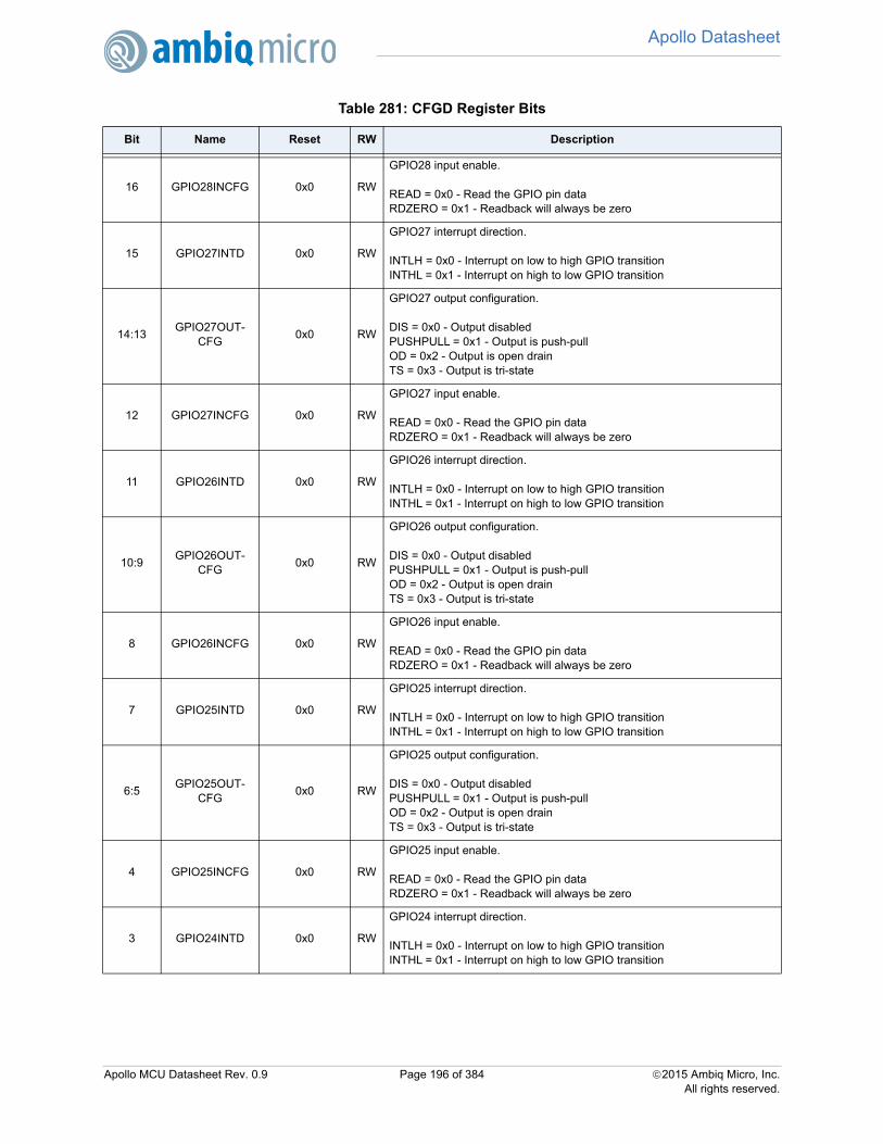
Apollo Datasheet
223
16 GPIO28INCFG 0x0 RW
GPIO28 input enable.
READ = 0x0 - Read the GPIO pin dataRDZERO = 0x1 - Readback will always be zero
15 GPIO27INTD 0x0 RW
GPIO27 interrupt direction.
INTLH = 0x0 - Interrupt on low to high GPIO transitionINTHL = 0x1 - Interrupt on high to low GPIO transition
14:13GPIO27OUT-
CFG0x0 RW
GPIO27 output configuration.
DIS = 0x0 - Output disabledPUSHPULL = 0x1 - Output is push-pullOD = 0x2 - Output is open drainTS = 0x3 - Output is tri-state
12 GPIO27INCFG 0x0 RW
GPIO27 input enable.
READ = 0x0 - Read the GPIO pin dataRDZERO = 0x1 - Readback will always be zero
11 GPIO26INTD 0x0 RW
GPIO26 interrupt direction.
INTLH = 0x0 - Interrupt on low to high GPIO transitionINTHL = 0x1 - Interrupt on high to low GPIO transition
10:9GPIO26OUT-
CFG0x0 RW
GPIO26 output configuration.
DIS = 0x0 - Output disabledPUSHPULL = 0x1 - Output is push-pullOD = 0x2 - Output is open drainTS = 0x3 - Output is tri-state
8 GPIO26INCFG 0x0 RW
GPIO26 input enable.
READ = 0x0 - Read the GPIO pin dataRDZERO = 0x1 - Readback will always be zero
7 GPIO25INTD 0x0 RW
GPIO25 interrupt direction.
INTLH = 0x0 - Interrupt on low to high GPIO transitionINTHL = 0x1 - Interrupt on high to low GPIO transition
6:5GPIO25OUT-
CFG0x0 RW
GPIO25 output configuration.
DIS = 0x0 - Output disabledPUSHPULL = 0x1 - Output is push-pullOD = 0x2 - Output is open drainTS = 0x3 - Output is tri-state
4 GPIO25INCFG 0x0 RW
GPIO25 input enable.
READ = 0x0 - Read the GPIO pin dataRDZERO = 0x1 - Readback will always be zero
3 GPIO24INTD 0x0 RW
GPIO24 interrupt direction.
INTLH = 0x0 - Interrupt on low to high GPIO transitionINTHL = 0x1 - Interrupt on high to low GPIO transition
Table 281: CFGD Register Bits
Bit Name Reset RW Description
Apollo MCU Datasheet Rev. 0.9 Page 196 of 384 2015 Ambiq Micro, Inc.All rights reserved.

Apollo Datasheet
223
7.6.2.18 CFGE Register
GPIO Configuration Register E
OFFSET: 0x00000050
INSTANCE 0 ADDRESS: 0x40010050
GPIO configuration controls for GPIO[39:32]. Writes to this register must be unlocked by the PADKEYregister.
2:1GPIO24OUT-
CFG0x0 RW
GPIO24 output configuration.
DIS = 0x0 - Output disabledPUSHPULL = 0x1 - Output is push-pullOD = 0x2 - Output is open drainTS = 0x3 - Output is tri-state
0 GPIO24INCFG 0x0 RW
GPIO24 input enable.
READ = 0x0 - Read the GPIO pin dataRDZERO = 0x1 - Readback will always be zero
Table 282: CFGE Register
31
30
29
28
27
26
25
24
23
22
21
20
19
18
17
16
15
14
13
12
11
10
09
08
07
06
05
04
03
02
01
00
GP
IO39
INT
D
GP
IO39
OU
TC
FG
GP
IO39
INC
FG
GP
IO38
INT
D
GP
IO38
OU
TC
FG
GP
IO38
INC
FG
GP
IO37
INT
D
GP
IO37
OU
TC
FG
GP
IO37
INC
FG
GP
IO36
INT
D
GP
IO36
OU
TC
FG
GP
IO36
INC
FG
GP
IO35
INT
D
GP
IO35
OU
TC
FG
GP
IO35
INC
FG
GP
IO34
INT
D
GP
IO34
OU
TC
FG
GP
IO34
INC
FG
GP
IO33
INT
D
GP
IO33
OU
TC
FG
GP
IO33
INC
FG
GP
IO32
INT
D
GP
IO32
OU
TC
FG
GP
IO32
INC
FG
Table 283: CFGE Register Bits
Bit Name Reset RW Description
31 GPIO39INTD 0x0 RW
GPIO39 interrupt direction.
INTLH = 0x0 - Interrupt on low to high GPIO transitionINTHL = 0x1 - Interrupt on high to low GPIO transition
30:29GPIO39OUT-
CFG0x0 RW
GPIO39 output configuration.
DIS = 0x0 - Output disabledPUSHPULL = 0x1 - Output is push-pullOD = 0x2 - Output is open drainTS = 0x3 - Output is tri-state
28 GPIO39INCFG 0x0 RW
GPIO39 input enable.
READ = 0x0 - Read the GPIO pin dataRDZERO = 0x1 - Readback will always be zero
Table 281: CFGD Register Bits
Bit Name Reset RW Description
Apollo MCU Datasheet Rev. 0.9 Page 197 of 384 2015 Ambiq Micro, Inc.All rights reserved.

Apollo Datasheet
223
27 GPIO38INTD 0x0 RW
GPIO38 interrupt direction.
INTLH = 0x0 - Interrupt on low to high GPIO transitionINTHL = 0x1 - Interrupt on high to low GPIO transition
26:25GPIO38OUT-
CFG0x0 RW
GPIO38 output configuration.
DIS = 0x0 - Output disabledPUSHPULL = 0x1 - Output is push-pullOD = 0x2 - Output is open drainTS = 0x3 - Output is tri-state
24 GPIO38INCFG 0x0 RW
GPIO38 input enable.
READ = 0x0 - Read the GPIO pin dataRDZERO = 0x1 - Readback will always be zero
23 GPIO37INTD 0x0 RW
GPIO37 interrupt direction.
INTLH = 0x0 - Interrupt on low to high GPIO transitionINTHL = 0x1 - Interrupt on high to low GPIO transition
22:21GPIO37OUT-
CFG0x0 RW
GPIO37 output configuration.
DIS = 0x0 - Output disabledPUSHPULL = 0x1 - Output is push-pullOD = 0x2 - Output is open drainTS = 0x3 - Output is tri-state
20 GPIO37INCFG 0x0 RW
GPIO37 input enable.
READ = 0x0 - Read the GPIO pin dataRDZERO = 0x1 - Readback will always be zero
19 GPIO36INTD 0x0 RW
GPIO36 interrupt direction.
INTLH = 0x0 - Interrupt on low to high GPIO transitionINTHL = 0x1 - Interrupt on high to low GPIO transition
18:17GPIO36OUT-
CFG0x0 RW
GPIO36 output configuration.
DIS = 0x0 - Output disabledPUSHPULL = 0x1 - Output is push-pullOD = 0x2 - Output is open drainTS = 0x3 - Output is tri-state
16 GPIO36INCFG 0x0 RW
GPIO36 input enable.
READ = 0x0 - Read the GPIO pin dataRDZERO = 0x1 - Readback will always be zero
15 GPIO35INTD 0x0 RW
GPIO35 interrupt direction.
INTLH = 0x0 - Interrupt on low to high GPIO transitionINTHL = 0x1 - Interrupt on high to low GPIO transition
14:13GPIO35OUT-
CFG0x0 RW
GPIO35 output configuration.
DIS = 0x0 - Output disabledPUSHPULL = 0x1 - Output is push-pullOD = 0x2 - Output is open drainTS = 0x3 - Output is tri-state
Table 283: CFGE Register Bits
Bit Name Reset RW Description
Apollo MCU Datasheet Rev. 0.9 Page 198 of 384 2015 Ambiq Micro, Inc.All rights reserved.

Apollo Datasheet
223
7.6.2.19 CFGF Register
GPIO Configuration Register F
OFFSET: 0x00000054
INSTANCE 0 ADDRESS: 0x40010054
12 GPIO35INCFG 0x0 RW
GPIO35 input enable.
READ = 0x0 - Read the GPIO pin dataRDZERO = 0x1 - Readback will always be zero
11 GPIO34INTD 0x0 RW
GPIO34 interrupt direction.
INTLH = 0x0 - Interrupt on low to high GPIO transitionINTHL = 0x1 - Interrupt on high to low GPIO transition
10:9GPIO34OUT-
CFG0x0 RW
GPIO34 output configuration.
DIS = 0x0 - Output disabledPUSHPULL = 0x1 - Output is push-pullOD = 0x2 - Output is open drainTS = 0x3 - Output is tri-state
8 GPIO34INCFG 0x0 RW
GPIO34 input enable.
READ = 0x0 - Read the GPIO pin dataRDZERO = 0x1 - Readback will always be zero
7 GPIO33INTD 0x0 RW
GPIO33 interrupt direction.
INTLH = 0x0 - Interrupt on low to high GPIO transitionINTHL = 0x1 - Interrupt on high to low GPIO transition
6:5GPIO33OUT-
CFG0x0 RW
GPIO33 output configuration.
DIS = 0x0 - Output disabledPUSHPULL = 0x1 - Output is push-pullOD = 0x2 - Output is open drainTS = 0x3 - Output is tri-state
4 GPIO33INCFG 0x0 RW
GPIO33 input enable.
READ = 0x0 - Read the GPIO pin dataRDZERO = 0x1 - Readback will always be zero
3 GPIO32INTD 0x0 RW
GPIO32 interrupt direction.
INTLH = 0x0 - Interrupt on low to high GPIO transitionINTHL = 0x1 - Interrupt on high to low GPIO transition
2:1GPIO32OUT-
CFG0x0 RW
GPIO32 output configuration.
DIS = 0x0 - Output disabledPUSHPULL = 0x1 - Output is push-pullOD = 0x2 - Output is open drainTS = 0x3 - Output is tri-state
0 GPIO32INCFG 0x0 RW
GPIO32 input enable.
READ = 0x0 - Read the GPIO pin dataRDZERO = 0x1 - Readback will always be zero
Table 283: CFGE Register Bits
Bit Name Reset RW Description
Apollo MCU Datasheet Rev. 0.9 Page 199 of 384 2015 Ambiq Micro, Inc.All rights reserved.

Apollo Datasheet
223
GPIO configuration controls for GPIO[47:40]. Writes to this register must be unlocked by the PADKEYregister.Table 284: CFGF Register
31
30
29
28
27
26
25
24
23
22
21
20
19
18
17
16
15
14
13
12
11
10
09
08
07
06
05
04
03
02
01
00
GP
IO47
INT
D
GP
IO47
OU
TC
FG
GP
IO47
INC
FG
GP
IO46
INT
D
GP
IO46
OU
TC
FG
GP
IO46
INC
FG
GP
IO45
INT
D
GP
IO45
OU
TC
FG
GP
IO45
INC
FG
GP
IO44
INT
D
GP
IO44
OU
TC
FG
GP
IO44
INC
FG
GP
IO43
INT
D
GP
IO43
OU
TC
FG
GP
IO43
INC
FG
GP
IO42
INT
D
GP
IO42
OU
TC
FG
GP
IO42
INC
FG
GP
IO41
INT
D
GP
IO41
OU
TC
FG
GP
IO41
INC
FG
GP
IO40
INT
D
GP
IO40
OU
TC
FG
GP
IO40
INC
FG
Table 285: CFGF Register Bits
Bit Name Reset RW Description
31 GPIO47INTD 0x0 RW
GPIO47 interrupt direction.
INTLH = 0x0 - Interrupt on low to high GPIO transitionINTHL = 0x1 - Interrupt on high to low GPIO transition
30:29GPIO47OUT-
CFG0x0 RW
GPIO47 output configuration.
DIS = 0x0 - Output disabledPUSHPULL = 0x1 - Output is push-pullOD = 0x2 - Output is open drainTS = 0x3 - Output is tri-state
28 GPIO47INCFG 0x0 RW
GPIO47 input enable.
READ = 0x0 - Read the GPIO pin dataRDZERO = 0x1 - Readback will always be zero
27 GPIO46INTD 0x0 RW
GPIO46 interrupt direction.
INTLH = 0x0 - Interrupt on low to high GPIO transitionINTHL = 0x1 - Interrupt on high to low GPIO transition
26:25GPIO46OUT-
CFG0x0 RW
GPIO46 output configuration.
DIS = 0x0 - Output disabledPUSHPULL = 0x1 - Output is push-pullOD = 0x2 - Output is open drainTS = 0x3 - Output is tri-state
24 GPIO46INCFG 0x0 RW
GPIO46 input enable.
READ = 0x0 - Read the GPIO pin dataRDZERO = 0x1 - Readback will always be zero
23 GPIO45INTD 0x0 RW
GPIO45 interrupt direction.
INTLH = 0x0 - Interrupt on low to high GPIO transitionINTHL = 0x1 - Interrupt on high to low GPIO transition
Apollo MCU Datasheet Rev. 0.9 Page 200 of 384 2015 Ambiq Micro, Inc.All rights reserved.

Apollo Datasheet
223
22:21GPIO45OUT-
CFG0x0 RW
GPIO45 output configuration.
DIS = 0x0 - Output disabledPUSHPULL = 0x1 - Output is push-pullOD = 0x2 - Output is open drainTS = 0x3 - Output is tri-state
20 GPIO45INCFG 0x0 RW
GPIO45 input enable.
READ = 0x0 - Read the GPIO pin dataRDZERO = 0x1 - Readback will always be zero
19 GPIO44INTD 0x0 RW
GPIO44 interrupt direction.
INTLH = 0x0 - Interrupt on low to high GPIO transitionINTHL = 0x1 - Interrupt on high to low GPIO transition
18:17GPIO44OUT-
CFG0x0 RW
GPIO44 output configuration.
DIS = 0x0 - Output disabledPUSHPULL = 0x1 - Output is push-pullOD = 0x2 - Output is open drainTS = 0x3 - Output is tri-state
16 GPIO44INCFG 0x0 RW
GPIO44 input enable.
READ = 0x0 - Read the GPIO pin dataRDZERO = 0x1 - Readback will always be zero
15 GPIO43INTD 0x0 RW
GPIO43 interrupt direction.
INTLH = 0x0 - Interrupt on low to high GPIO transitionINTHL = 0x1 - Interrupt on high to low GPIO transition
14:13GPIO43OUT-
CFG0x0 RW
GPIO43 output configuration.
DIS = 0x0 - Output disabledPUSHPULL = 0x1 - Output is push-pullOD = 0x2 - Output is open drainTS = 0x3 - Output is tri-state
12 GPIO43INCFG 0x0 RW
GPIO43 input enable.
READ = 0x0 - Read the GPIO pin dataRDZERO = 0x1 - Readback will always be zero
11 GPIO42INTD 0x0 RW
GPIO42 interrupt direction.
INTLH = 0x0 - Interrupt on low to high GPIO transitionINTHL = 0x1 - Interrupt on high to low GPIO transition
10:9GPIO42OUT-
CFG0x0 RW
GPIO42 output configuration.
DIS = 0x0 - Output disabledPUSHPULL = 0x1 - Output is push-pullOD = 0x2 - Output is open drainTS = 0x3 - Output is tri-state
8 GPIO42INCFG 0x0 RW
GPIO42 input enable.
READ = 0x0 - Read the GPIO pin dataRDZERO = 0x1 - Readback will always be zero
Table 285: CFGF Register Bits
Bit Name Reset RW Description
Apollo MCU Datasheet Rev. 0.9 Page 201 of 384 2015 Ambiq Micro, Inc.All rights reserved.

Apollo Datasheet
223
7.6.2.20 CFGG Register
GPIO Configuration Register G
OFFSET: 0x00000058
INSTANCE 0 ADDRESS: 0x40010058
GPIO configuration controls for GPIO[49:48]. Writes to this register must be unlocked by the PADKEYregister.
7 GPIO41INTD 0x0 RW
GPIO41 interrupt direction.
INTLH = 0x0 - Interrupt on low to high GPIO transitionINTHL = 0x1 - Interrupt on high to low GPIO transition
6:5GPIO41OUT-
CFG0x0 RW
GPIO41 output configuration.
DIS = 0x0 - Output disabledPUSHPULL = 0x1 - Output is push-pullOD = 0x2 - Output is open drainTS = 0x3 - Output is tri-state
4 GPIO41INCFG 0x0 RW
GPIO41 input enable.
READ = 0x0 - Read the GPIO pin dataRDZERO = 0x1 - Readback will always be zero
3 GPIO40INTD 0x0 RW
GPIO40 interrupt direction.
INTLH = 0x0 - Interrupt on low to high GPIO transitionINTHL = 0x1 - Interrupt on high to low GPIO transition
2:1GPIO40OUT-
CFG0x0 RW
GPIO40 output configuration.
DIS = 0x0 - Output disabledPUSHPULL = 0x1 - Output is push-pullOD = 0x2 - Output is open drainTS = 0x3 - Output is tri-state
0 GPIO40INCFG 0x0 RW
GPIO40 input enable.
READ = 0x0 - Read the GPIO pin dataRDZERO = 0x1 - Readback will always be zero
Table 286: CFGG Register
31
30
29
28
27
26
25
24
23
22
21
20
19
18
17
16
15
14
13
12
11
10
09
08
07
06
05
04
03
02
01
00
RSVD
GP
IO49
INT
D
GP
IO49
OU
TC
FG
GP
IO49
INC
FG
GP
IO48
INT
D
GP
IO48
OU
TC
FG
GP
IO48
INC
FG
Table 285: CFGF Register Bits
Bit Name Reset RW Description
Apollo MCU Datasheet Rev. 0.9 Page 202 of 384 2015 Ambiq Micro, Inc.All rights reserved.

Apollo Datasheet
223
7.6.2.21 PADKEY Register
Key Register for all pad configuration registers
OFFSET: 0x00000060
INSTANCE 0 ADDRESS: 0x40010060
Key Register for all pad configuration registers
Table 287: CFGG Register Bits
Bit Name Reset RW Description
31:8 RSVD 0x0 RORESERVED
7 GPIO49INTD 0x0 RW
GPIO49 interrupt direction.
INTLH = 0x0 - Interrupt on low to high GPIO transitionINTHL = 0x1 - Interrupt on high to low GPIO transition
6:5GPIO49OUT-
CFG0x0 RW
GPIO49 output configuration.
DIS = 0x0 - Output disabledPUSHPULL = 0x1 - Output is push-pullOD = 0x2 - Output is open drainTS = 0x3 - Output is tri-state
4 GPIO49INCFG 0x0 RW
GPIO49 input enable.
READ = 0x0 - Read the GPIO pin dataRDZERO = 0x1 - Readback will always be zero
3 GPIO48INTD 0x0 RW
GPIO48 interrupt direction.
INTLH = 0x0 - Interrupt on low to high GPIO transitionINTHL = 0x1 - Interrupt on high to low GPIO transition
2:1GPIO48OUT-
CFG0x0 RW
GPIO48 output configuration.
DIS = 0x0 - Output disabledPUSHPULL = 0x1 - Output is push-pullOD = 0x2 - Output is open drainTS = 0x3 - Output is tri-state
0 GPIO48INCFG 0x0 RW
GPIO48 input enable.
READ = 0x0 - Read the GPIO pin dataRDZERO = 0x1 - Readback will always be zero
Table 288: PADKEY Register
31
30
29
28
27
26
25
24
23
22
21
20
19
18
17
16
15
14
13
12
11
10
09
08
07
06
05
04
03
02
01
00
PADKEY
Apollo MCU Datasheet Rev. 0.9 Page 203 of 384 2015 Ambiq Micro, Inc.All rights reserved.

Apollo Datasheet
223
7.6.2.22 RDA Register
GPIO Input Register A
OFFSET: 0x00000080
INSTANCE 0 ADDRESS: 0x40010080
GPIO Input Register A
7.6.2.23 RDB Register
GPIO Input Register B
OFFSET: 0x00000084
INSTANCE 0 ADDRESS: 0x40010084
GPIO Input Register B
Table 289: PADKEY Register Bits
Bit Name Reset RW Description
31:0 PADKEY 0x0 RWKey register value.
Key = 0x73 - Key
Table 290: RDA Register
31
30
29
28
27
26
25
24
23
22
21
20
19
18
17
16
15
14
13
12
11
10
09
08
07
06
05
04
03
02
01
00
RDA
Table 291: RDA Register Bits
Bit Name Reset RW Description
31:0 RDA 0x0 ROGPIO31-0 read data.
Table 292: RDB Register
31
30
29
28
27
26
25
24
23
22
21
20
19
18
17
16
15
14
13
12
11
10
09
08
07
06
05
04
03
02
01
00
RSVD RDB
Apollo MCU Datasheet Rev. 0.9 Page 204 of 384 2015 Ambiq Micro, Inc.All rights reserved.

Apollo Datasheet
223
7.6.2.24 WTA Register
GPIO Output Register A
OFFSET: 0x00000088
INSTANCE 0 ADDRESS: 0x40010088
GPIO Output Register A
7.6.2.25 WTB Register
GPIO Output Register B
OFFSET: 0x0000008C
INSTANCE 0 ADDRESS: 0x4001008C
GPIO Output Register B
Table 293: RDB Register Bits
Bit Name Reset RW Description
31:18 RSVD 0x0 RORESERVED
17:0 RDB 0x0 ROGPIO49-32 read data.
Table 294: WTA Register
31
30
29
28
27
26
25
24
23
22
21
20
19
18
17
16
15
14
13
12
11
10
09
08
07
06
05
04
03
02
01
00
WTA
Table 295: WTA Register Bits
Bit Name Reset RW Description
31:0 WTA 0x0 RWGPIO31-0 write data.
Table 296: WTB Register
31
30
29
28
27
26
25
24
23
22
21
20
19
18
17
16
15
14
13
12
11
10
09
08
07
06
05
04
03
02
01
00
RSVD WTB
Apollo MCU Datasheet Rev. 0.9 Page 205 of 384 2015 Ambiq Micro, Inc.All rights reserved.

Apollo Datasheet
223
7.6.2.26 WTSA Register
GPIO Output Register A Set
OFFSET: 0x00000090
INSTANCE 0 ADDRESS: 0x40010090
GPIO Output Register A Set
7.6.2.27 WTSB Register
GPIO Output Register B Set
OFFSET: 0x00000094
INSTANCE 0 ADDRESS: 0x40010094
GPIO Output Register B Set
Table 297: WTB Register Bits
Bit Name Reset RW Description
31:18 RSVD 0x0 RORESERVED
17:0 WTB 0x0 RWGPIO49-32 write data.
Table 298: WTSA Register
31
30
29
28
27
26
25
24
23
22
21
20
19
18
17
16
15
14
13
12
11
10
09
08
07
06
05
04
03
02
01
00
WTSA
Table 299: WTSA Register Bits
Bit Name Reset RW Description
31:0 WTSA 0x0 WOSet the GPIO31-0 write data.
Table 300: WTSB Register
31
30
29
28
27
26
25
24
23
22
21
20
19
18
17
16
15
14
13
12
11
10
09
08
07
06
05
04
03
02
01
00
RSVD WTSB
Apollo MCU Datasheet Rev. 0.9 Page 206 of 384 2015 Ambiq Micro, Inc.All rights reserved.

Apollo Datasheet
223
7.6.2.28 WTCA Register
GPIO Output Register A Clear
OFFSET: 0x00000098
INSTANCE 0 ADDRESS: 0x40010098
GPIO Output Register A Clear
7.6.2.29 WTCB Register
GPIO Output Register B Clear
OFFSET: 0x0000009C
INSTANCE 0 ADDRESS: 0x4001009C
GPIO Output Register B Clear
Table 301: WTSB Register Bits
Bit Name Reset RW Description
31:18 RSVD 0x0 RORESERVED
17:0 WTSB 0x0 WOSet the GPIO49-32 write data.
Table 302: WTCA Register
31
30
29
28
27
26
25
24
23
22
21
20
19
18
17
16
15
14
13
12
11
10
09
08
07
06
05
04
03
02
01
00
WTCA
Table 303: WTCA Register Bits
Bit Name Reset RW Description
31:0 WTCA 0x0 WOClear the GPIO31-0 write data.
Table 304: WTCB Register
31
30
29
28
27
26
25
24
23
22
21
20
19
18
17
16
15
14
13
12
11
10
09
08
07
06
05
04
03
02
01
00
RSVD WTCB
Apollo MCU Datasheet Rev. 0.9 Page 207 of 384 2015 Ambiq Micro, Inc.All rights reserved.

Apollo Datasheet
223
7.6.2.30 ENA Register
GPIO Enable Register A
OFFSET: 0x000000A0
INSTANCE 0 ADDRESS: 0x400100A0
GPIO Enable Register A
7.6.2.31 ENB Register
GPIO Enable Register B
OFFSET: 0x000000A4
INSTANCE 0 ADDRESS: 0x400100A4
GPIO Enable Register B
Table 305: WTCB Register Bits
Bit Name Reset RW Description
31:18 RSVD 0x0 RORESERVED
17:0 WTCB 0x0 WOClear the GPIO49-32 write data.
Table 306: ENA Register
31
30
29
28
27
26
25
24
23
22
21
20
19
18
17
16
15
14
13
12
11
10
09
08
07
06
05
04
03
02
01
00
ENA
Table 307: ENA Register Bits
Bit Name Reset RW Description
31:0 ENA 0x0 RWGPIO31-0 output enables
Table 308: ENB Register
31
30
29
28
27
26
25
24
23
22
21
20
19
18
17
16
15
14
13
12
11
10
09
08
07
06
05
04
03
02
01
00
RSVD ENB
Apollo MCU Datasheet Rev. 0.9 Page 208 of 384 2015 Ambiq Micro, Inc.All rights reserved.

Apollo Datasheet
223
7.6.2.32 ENSA Register
GPIO Enable Register A Set
OFFSET: 0x000000A8
INSTANCE 0 ADDRESS: 0x400100A8
GPIO Enable Register A Set
7.6.2.33 ENSB Register
GPIO Enable Register B Set
OFFSET: 0x000000AC
INSTANCE 0 ADDRESS: 0x400100AC
GPIO Enable Register B Set
Table 309: ENB Register Bits
Bit Name Reset RW Description
31:18 RSVD 0x0 RORESERVED
17:0 ENB 0x0 RWGPIO49-32 output enables
Table 310: ENSA Register
31
30
29
28
27
26
25
24
23
22
21
20
19
18
17
16
15
14
13
12
11
10
09
08
07
06
05
04
03
02
01
00
ENSA
Table 311: ENSA Register Bits
Bit Name Reset RW Description
31:0 ENSA 0x0 RWSet the GPIO31-0 output enables
Table 312: ENSB Register
31
30
29
28
27
26
25
24
23
22
21
20
19
18
17
16
15
14
13
12
11
10
09
08
07
06
05
04
03
02
01
00
RSVD ENSB
Apollo MCU Datasheet Rev. 0.9 Page 209 of 384 2015 Ambiq Micro, Inc.All rights reserved.

Apollo Datasheet
223
7.6.2.34 ENCA Register
GPIO Enable Register A Clear
OFFSET: 0x000000B4
INSTANCE 0 ADDRESS: 0x400100B4
GPIO Enable Register A Clear
7.6.2.35 ENCB Register
GPIO Enable Register B Clear
OFFSET: 0x000000B8
INSTANCE 0 ADDRESS: 0x400100B8
GPIO Enable Register B Clear
Table 313: ENSB Register Bits
Bit Name Reset RW Description
31:18 RSVD 0x0 RORESERVED
17:0 ENSB 0x0 RWSet the GPIO49-32 output enables
Table 314: ENCA Register
31
30
29
28
27
26
25
24
23
22
21
20
19
18
17
16
15
14
13
12
11
10
09
08
07
06
05
04
03
02
01
00
ENCA
Table 315: ENCA Register Bits
Bit Name Reset RW Description
31:0 ENCA 0x0 RWClear the GPIO31-0 output enables
Table 316: ENCB Register
31
30
29
28
27
26
25
24
23
22
21
20
19
18
17
16
15
14
13
12
11
10
09
08
07
06
05
04
03
02
01
00
RSVD ENCB
Apollo MCU Datasheet Rev. 0.9 Page 210 of 384 2015 Ambiq Micro, Inc.All rights reserved.

Apollo Datasheet
223
7.6.2.36 INT0EN Register
GPIO Interrupt Registers 31-0: Enable
OFFSET: 0x00000200
INSTANCE 0 ADDRESS: 0x40010200
Set bits in this register to allow this module to generate the corresponding interrupt.
Table 317: ENCB Register Bits
Bit Name Reset RW Description
31:18 RSVD 0x0 RORESERVED
17:0 ENCB 0x0 RWClear the GPIO49-32 output enables
Table 318: INT0EN Register
31
30
29
28
27
26
25
24
23
22
21
20
19
18
17
16
15
14
13
12
11
10
09
08
07
06
05
04
03
02
01
00
GP
IO31
GP
IO30
GP
IO29
GP
IO28
GP
IO27
GP
IO26
GP
IO25
GP
IO24
GP
IO23
GP
IO22
GP
IO21
GP
IO20
GP
IO19
GP
IO18
GP
IO17
GP
IO16
GP
IO15
GP
IO14
GP
IO13
GP
IO12
GP
IO11
GP
IO10
GP
IO9
GP
IO8
GP
IO7
GP
IO6
GP
IO5
GP
IO4
GP
IO3
GP
IO2
GP
IO1
GP
IO0
Table 319: INT0EN Register Bits
Bit Name Reset RW Description
31 GPIO31 0x0 RWGPIO31 interrupt.
30 GPIO30 0x0 RWGPIO30 interrupt.
29 GPIO29 0x0 RWGPIO29 interrupt.
28 GPIO28 0x0 RWGPIO28 interrupt.
27 GPIO27 0x0 RWGPIO27 interrupt.
26 GPIO26 0x0 RWGPIO26 interrupt.
25 GPIO25 0x0 RWGPIO25 interrupt.
24 GPIO24 0x0 RWGPIO24 interrupt.
23 GPIO23 0x0 RWGPIO23 interrupt.
Apollo MCU Datasheet Rev. 0.9 Page 211 of 384 2015 Ambiq Micro, Inc.All rights reserved.

Apollo Datasheet
223
22 GPIO22 0x0 RWGPIO22 interrupt.
21 GPIO21 0x0 RWGPIO21 interrupt.
20 GPIO20 0x0 RWGPIO20 interrupt.
19 GPIO19 0x0 RWGPIO19 interrupt.
18 GPIO18 0x0 RWGPIO18interrupt.
17 GPIO17 0x0 RWGPIO17 interrupt.
16 GPIO16 0x0 RWGPIO16 interrupt.
15 GPIO15 0x0 RWGPIO15 interrupt.
14 GPIO14 0x0 RWGPIO14 interrupt.
13 GPIO13 0x0 RWGPIO13 interrupt.
12 GPIO12 0x0 RWGPIO12 interrupt.
11 GPIO11 0x0 RWGPIO11 interrupt.
10 GPIO10 0x0 RWGPIO10 interrupt.
9 GPIO9 0x0 RWGPIO9 interrupt.
8 GPIO8 0x0 RWGPIO8 interrupt.
7 GPIO7 0x0 RWGPIO7 interrupt.
6 GPIO6 0x0 RWGPIO6 interrupt.
5 GPIO5 0x0 RWGPIO5 interrupt.
4 GPIO4 0x0 RWGPIO4 interrupt.
3 GPIO3 0x0 RWGPIO3 interrupt.
2 GPIO2 0x0 RWGPIO2 interrupt.
1 GPIO1 0x0 RWGPIO1 interrupt.
0 GPIO0 0x0 RWGPIO0 interrupt.
Table 319: INT0EN Register Bits
Bit Name Reset RW Description
Apollo MCU Datasheet Rev. 0.9 Page 212 of 384 2015 Ambiq Micro, Inc.All rights reserved.

Apollo Datasheet
223
7.6.2.37 INT0STAT RegisterGPIO Interrupt Registers 31-0: Status
OFFSET: 0x00000204
INSTANCE 0 ADDRESS: 0x40010204
Read bits from this register to discover the cause of a recent interrupt.
Table 320: INT0STAT Register
31
30
29
28
27
26
25
24
23
22
21
20
19
18
17
16
15
14
13
12
11
10
09
08
07
06
05
04
03
02
01
00
GP
IO31
GP
IO30
GP
IO29
GP
IO28
GP
IO27
GP
IO26
GP
IO25
GP
IO24
GP
IO23
GP
IO22
GP
IO21
GP
IO20
GP
IO19
GP
IO18
GP
IO17
GP
IO16
GP
IO15
GP
IO14
GP
IO13
GP
IO12
GP
IO11
GP
IO10
GP
IO9
GP
IO8
GP
IO7
GP
IO6
GP
IO5
GP
IO4
GP
IO3
GP
IO2
GP
IO1
GP
IO0
Table 321: INT0STAT Register Bits
Bit Name Reset RW Description
31 GPIO31 0x0 RWGPIO31 interrupt.
30 GPIO30 0x0 RWGPIO30 interrupt.
29 GPIO29 0x0 RWGPIO29 interrupt.
28 GPIO28 0x0 RWGPIO28 interrupt.
27 GPIO27 0x0 RWGPIO27 interrupt.
26 GPIO26 0x0 RWGPIO26 interrupt.
25 GPIO25 0x0 RWGPIO25 interrupt.
24 GPIO24 0x0 RWGPIO24 interrupt.
23 GPIO23 0x0 RWGPIO23 interrupt.
22 GPIO22 0x0 RWGPIO22 interrupt.
21 GPIO21 0x0 RWGPIO21 interrupt.
20 GPIO20 0x0 RWGPIO20 interrupt.
19 GPIO19 0x0 RWGPIO19 interrupt.
18 GPIO18 0x0 RWGPIO18interrupt.
Apollo MCU Datasheet Rev. 0.9 Page 213 of 384 2015 Ambiq Micro, Inc.All rights reserved.

Apollo Datasheet
223
7.6.2.38 INT0CLR Register
GPIO Interrupt Registers 31-0: Clear
OFFSET: 0x00000208
INSTANCE 0 ADDRESS: 0x40010208
Write a 1 to a bit in this register to clear the interrupt status associated with that bit.
17 GPIO17 0x0 RWGPIO17 interrupt.
16 GPIO16 0x0 RWGPIO16 interrupt.
15 GPIO15 0x0 RWGPIO15 interrupt.
14 GPIO14 0x0 RWGPIO14 interrupt.
13 GPIO13 0x0 RWGPIO13 interrupt.
12 GPIO12 0x0 RWGPIO12 interrupt.
11 GPIO11 0x0 RWGPIO11 interrupt.
10 GPIO10 0x0 RWGPIO10 interrupt.
9 GPIO9 0x0 RWGPIO9 interrupt.
8 GPIO8 0x0 RWGPIO8 interrupt.
7 GPIO7 0x0 RWGPIO7 interrupt.
6 GPIO6 0x0 RWGPIO6 interrupt.
5 GPIO5 0x0 RWGPIO5 interrupt.
4 GPIO4 0x0 RWGPIO4 interrupt.
3 GPIO3 0x0 RWGPIO3 interrupt.
2 GPIO2 0x0 RWGPIO2 interrupt.
1 GPIO1 0x0 RWGPIO1 interrupt.
0 GPIO0 0x0 RWGPIO0 interrupt.
Table 321: INT0STAT Register Bits
Bit Name Reset RW Description
Apollo MCU Datasheet Rev. 0.9 Page 214 of 384 2015 Ambiq Micro, Inc.All rights reserved.

Apollo Datasheet
223
Table 322: INT0CLR Register
31
30
29
28
27
26
25
24
23
22
21
20
19
18
17
16
15
14
13
12
11
10
09
08
07
06
05
04
03
02
01
00
GP
IO31
GP
IO30
GP
IO29
GP
IO28
GP
IO27
GP
IO26
GP
IO25
GP
IO24
GP
IO23
GP
IO22
GP
IO21
GP
IO20
GP
IO19
GP
IO18
GP
IO17
GP
IO16
GP
IO15
GP
IO14
GP
IO13
GP
IO12
GP
IO11
GP
IO10
GP
IO9
GP
IO8
GP
IO7
GP
IO6
GP
IO5
GP
IO4
GP
IO3
GP
IO2
GP
IO1
GP
IO0
Table 323: INT0CLR Register Bits
Bit Name Reset RW Description
31 GPIO31 0x0 RWGPIO31 interrupt.
30 GPIO30 0x0 RWGPIO30 interrupt.
29 GPIO29 0x0 RWGPIO29 interrupt.
28 GPIO28 0x0 RWGPIO28 interrupt.
27 GPIO27 0x0 RWGPIO27 interrupt.
26 GPIO26 0x0 RWGPIO26 interrupt.
25 GPIO25 0x0 RWGPIO25 interrupt.
24 GPIO24 0x0 RWGPIO24 interrupt.
23 GPIO23 0x0 RWGPIO23 interrupt.
22 GPIO22 0x0 RWGPIO22 interrupt.
21 GPIO21 0x0 RWGPIO21 interrupt.
20 GPIO20 0x0 RWGPIO20 interrupt.
19 GPIO19 0x0 RWGPIO19 interrupt.
18 GPIO18 0x0 RWGPIO18interrupt.
17 GPIO17 0x0 RWGPIO17 interrupt.
16 GPIO16 0x0 RWGPIO16 interrupt.
15 GPIO15 0x0 RWGPIO15 interrupt.
14 GPIO14 0x0 RWGPIO14 interrupt.
Apollo MCU Datasheet Rev. 0.9 Page 215 of 384 2015 Ambiq Micro, Inc.All rights reserved.

Apollo Datasheet
223
7.6.2.39 INT0SET Register
GPIO Interrupt Registers 31-0: Set
OFFSET: 0x0000020C
INSTANCE 0 ADDRESS: 0x4001020C
Write a 1 to a bit in this register to instantly generate an interrupt from this module. (Generally used fortesting purposes).
13 GPIO13 0x0 RWGPIO13 interrupt.
12 GPIO12 0x0 RWGPIO12 interrupt.
11 GPIO11 0x0 RWGPIO11 interrupt.
10 GPIO10 0x0 RWGPIO10 interrupt.
9 GPIO9 0x0 RWGPIO9 interrupt.
8 GPIO8 0x0 RWGPIO8 interrupt.
7 GPIO7 0x0 RWGPIO7 interrupt.
6 GPIO6 0x0 RWGPIO6 interrupt.
5 GPIO5 0x0 RWGPIO5 interrupt.
4 GPIO4 0x0 RWGPIO4 interrupt.
3 GPIO3 0x0 RWGPIO3 interrupt.
2 GPIO2 0x0 RWGPIO2 interrupt.
1 GPIO1 0x0 RWGPIO1 interrupt.
0 GPIO0 0x0 RWGPIO0 interrupt.
Table 324: INT0SET Register
31
30
29
28
27
26
25
24
23
22
21
20
19
18
17
16
15
14
13
12
11
10
09
08
07
06
05
04
03
02
01
00
GP
IO31
GP
IO30
GP
IO29
GP
IO28
GP
IO27
GP
IO26
GP
IO25
GP
IO24
GP
IO23
GP
IO22
GP
IO21
GP
IO20
GP
IO19
GP
IO18
GP
IO17
GP
IO16
GP
IO15
GP
IO14
GP
IO13
GP
IO12
GP
IO11
GP
IO10
GP
IO9
GP
IO8
GP
IO7
GP
IO6
GP
IO5
GP
IO4
GP
IO3
GP
IO2
GP
IO1
GP
IO0
Table 323: INT0CLR Register Bits
Bit Name Reset RW Description
Apollo MCU Datasheet Rev. 0.9 Page 216 of 384 2015 Ambiq Micro, Inc.All rights reserved.

Apollo Datasheet
223
Table 325: INT0SET Register Bits
Bit Name Reset RW Description
31 GPIO31 0x0 RWGPIO31 interrupt.
30 GPIO30 0x0 RWGPIO30 interrupt.
29 GPIO29 0x0 RWGPIO29 interrupt.
28 GPIO28 0x0 RWGPIO28 interrupt.
27 GPIO27 0x0 RWGPIO27 interrupt.
26 GPIO26 0x0 RWGPIO26 interrupt.
25 GPIO25 0x0 RWGPIO25 interrupt.
24 GPIO24 0x0 RWGPIO24 interrupt.
23 GPIO23 0x0 RWGPIO23 interrupt.
22 GPIO22 0x0 RWGPIO22 interrupt.
21 GPIO21 0x0 RWGPIO21 interrupt.
20 GPIO20 0x0 RWGPIO20 interrupt.
19 GPIO19 0x0 RWGPIO19 interrupt.
18 GPIO18 0x0 RWGPIO18interrupt.
17 GPIO17 0x0 RWGPIO17 interrupt.
16 GPIO16 0x0 RWGPIO16 interrupt.
15 GPIO15 0x0 RWGPIO15 interrupt.
14 GPIO14 0x0 RWGPIO14 interrupt.
13 GPIO13 0x0 RWGPIO13 interrupt.
12 GPIO12 0x0 RWGPIO12 interrupt.
11 GPIO11 0x0 RWGPIO11 interrupt.
10 GPIO10 0x0 RWGPIO10 interrupt.
Apollo MCU Datasheet Rev. 0.9 Page 217 of 384 2015 Ambiq Micro, Inc.All rights reserved.

Apollo Datasheet
223
7.6.2.40 INT1EN Register
GPIO Interrupt Registers 49-32: Enable
OFFSET: 0x00000210
INSTANCE 0 ADDRESS: 0x40010210
Set bits in this register to allow this module to generate the corresponding interrupt.
9 GPIO9 0x0 RWGPIO9 interrupt.
8 GPIO8 0x0 RWGPIO8 interrupt.
7 GPIO7 0x0 RWGPIO7 interrupt.
6 GPIO6 0x0 RWGPIO6 interrupt.
5 GPIO5 0x0 RWGPIO5 interrupt.
4 GPIO4 0x0 RWGPIO4 interrupt.
3 GPIO3 0x0 RWGPIO3 interrupt.
2 GPIO2 0x0 RWGPIO2 interrupt.
1 GPIO1 0x0 RWGPIO1 interrupt.
0 GPIO0 0x0 RWGPIO0 interrupt.
Table 326: INT1EN Register
31
30
29
28
27
26
25
24
23
22
21
20
19
18
17
16
15
14
13
12
11
10
09
08
07
06
05
04
03
02
01
00
RSVD
GP
IO4
9
GP
IO4
8
GP
IO4
7
GP
IO4
6
GP
IO4
5
GP
IO4
4
GP
IO4
3
GP
IO4
2
GP
IO4
1
GP
IO4
0
GP
IO3
9
GP
IO3
8
GP
IO3
7
GP
IO3
6
GP
IO3
5
GP
IO3
4
GP
IO3
3
GP
IO3
2
Table 327: INT1EN Register Bits
Bit Name Reset RW Description
31:18 RSVD 0x0 RORESERVED
17 GPIO49 0x0 RWGPIO49 interrupt.
Table 325: INT0SET Register Bits
Bit Name Reset RW Description
Apollo MCU Datasheet Rev. 0.9 Page 218 of 384 2015 Ambiq Micro, Inc.All rights reserved.

Apollo Datasheet
223
7.6.2.41 INT1STAT Register
GPIO Interrupt Registers 49-32: Status
OFFSET: 0x00000214
INSTANCE 0 ADDRESS: 0x40010214
Read bits from this register to discover the cause of a recent interrupt.
16 GPIO48 0x0 RWGPIO48 interrupt.
15 GPIO47 0x0 RWGPIO47 interrupt.
14 GPIO46 0x0 RWGPIO46 interrupt.
13 GPIO45 0x0 RWGPIO45 interrupt.
12 GPIO44 0x0 RWGPIO44 interrupt.
11 GPIO43 0x0 RWGPIO43 interrupt.
10 GPIO42 0x0 RWGPIO42 interrupt.
9 GPIO41 0x0 RWGPIO41 interrupt.
8 GPIO40 0x0 RWGPIO40 interrupt.
7 GPIO39 0x0 RWGPIO39 interrupt.
6 GPIO38 0x0 RWGPIO38 interrupt.
5 GPIO37 0x0 RWGPIO37 interrupt.
4 GPIO36 0x0 RWGPIO36 interrupt.
3 GPIO35 0x0 RWGPIO35 interrupt.
2 GPIO34 0x0 RWGPIO34 interrupt.
1 GPIO33 0x0 RWGPIO33 interrupt.
0 GPIO32 0x0 RWGPIO32 interrupt.
Table 327: INT1EN Register Bits
Bit Name Reset RW Description
Apollo MCU Datasheet Rev. 0.9 Page 219 of 384 2015 Ambiq Micro, Inc.All rights reserved.

Apollo Datasheet
223
Table 328: INT1STAT Register
31
30
29
28
27
26
25
24
23
22
21
20
19
18
17
16
15
14
13
12
11
10
09
08
07
06
05
04
03
02
01
00
RSVD
GP
IO49
GP
IO48
GP
IO47
GP
IO46
GP
IO45
GP
IO44
GP
IO43
GP
IO42
GP
IO41
GP
IO40
GP
IO39
GP
IO38
GP
IO37
GP
IO36
GP
IO35
GP
IO34
GP
IO33
GP
IO32
Table 329: INT1STAT Register Bits
Bit Name Reset RW Description
31:18 RSVD 0x0 RORESERVED
17 GPIO49 0x0 RWGPIO49 interrupt.
16 GPIO48 0x0 RWGPIO48 interrupt.
15 GPIO47 0x0 RWGPIO47 interrupt.
14 GPIO46 0x0 RWGPIO46 interrupt.
13 GPIO45 0x0 RWGPIO45 interrupt.
12 GPIO44 0x0 RWGPIO44 interrupt.
11 GPIO43 0x0 RWGPIO43 interrupt.
10 GPIO42 0x0 RWGPIO42 interrupt.
9 GPIO41 0x0 RWGPIO41 interrupt.
8 GPIO40 0x0 RWGPIO40 interrupt.
7 GPIO39 0x0 RWGPIO39 interrupt.
6 GPIO38 0x0 RWGPIO38 interrupt.
5 GPIO37 0x0 RWGPIO37 interrupt.
4 GPIO36 0x0 RWGPIO36 interrupt.
3 GPIO35 0x0 RWGPIO35 interrupt.
2 GPIO34 0x0 RWGPIO34 interrupt.
1 GPIO33 0x0 RWGPIO33 interrupt.
Apollo MCU Datasheet Rev. 0.9 Page 220 of 384 2015 Ambiq Micro, Inc.All rights reserved.

Apollo Datasheet
223
7.6.2.42 INT1CLR Register
GPIO Interrupt Registers 49-32: Clear
OFFSET: 0x00000218
INSTANCE 0 ADDRESS: 0x40010218
Write a 1 to a bit in this register to clear the interrupt status associated with that bit.
0 GPIO32 0x0 RWGPIO32 interrupt.
Table 330: INT1CLR Register
31
30
29
28
27
26
25
24
23
22
21
20
19
18
17
16
15
14
13
12
11
10
09
08
07
06
05
04
03
02
01
00
RSVD
GP
IO49
GP
IO48
GP
IO47
GP
IO46
GP
IO45
GP
IO44
GP
IO43
GP
IO42
GP
IO41
GP
IO40
GP
IO39
GP
IO38
GP
IO37
GP
IO36
GP
IO35
GP
IO34
GP
IO33
GP
IO32
Table 331: INT1CLR Register Bits
Bit Name Reset RW Description
31:18 RSVD 0x0 RORESERVED
17 GPIO49 0x0 RWGPIO49 interrupt.
16 GPIO48 0x0 RWGPIO48 interrupt.
15 GPIO47 0x0 RWGPIO47 interrupt.
14 GPIO46 0x0 RWGPIO46 interrupt.
13 GPIO45 0x0 RWGPIO45 interrupt.
12 GPIO44 0x0 RWGPIO44 interrupt.
11 GPIO43 0x0 RWGPIO43 interrupt.
10 GPIO42 0x0 RWGPIO42 interrupt.
9 GPIO41 0x0 RWGPIO41 interrupt.
8 GPIO40 0x0 RWGPIO40 interrupt.
Table 329: INT1STAT Register Bits
Bit Name Reset RW Description
Apollo MCU Datasheet Rev. 0.9 Page 221 of 384 2015 Ambiq Micro, Inc.All rights reserved.

Apollo Datasheet
223
7.6.2.43 INT1SET Register
GPIO Interrupt Registers 49-32: Set
OFFSET: 0x0000021C
INSTANCE 0 ADDRESS: 0x4001021C
Write a 1 to a bit in this register to instantly generate an interrupt from this module. (Generally used fortesting purposes).
7 GPIO39 0x0 RWGPIO39 interrupt.
6 GPIO38 0x0 RWGPIO38 interrupt.
5 GPIO37 0x0 RWGPIO37 interrupt.
4 GPIO36 0x0 RWGPIO36 interrupt.
3 GPIO35 0x0 RWGPIO35 interrupt.
2 GPIO34 0x0 RWGPIO34 interrupt.
1 GPIO33 0x0 RWGPIO33 interrupt.
0 GPIO32 0x0 RWGPIO32 interrupt.
Table 332: INT1SET Register
31
30
29
28
27
26
25
24
23
22
21
20
19
18
17
16
15
14
13
12
11
10
09
08
07
06
05
04
03
02
01
00
RSVD
GP
IO49
GP
IO48
GP
IO47
GP
IO46
GP
IO45
GP
IO44
GP
IO43
GP
IO42
GP
IO41
GP
IO40
GP
IO39
GP
IO38
GP
IO37
GP
IO36
GP
IO35
GP
IO34
GP
IO33
GP
IO32
Table 333: INT1SET Register Bits
Bit Name Reset RW Description
31:18 RSVD 0x0 RORESERVED
17 GPIO49 0x0 RWGPIO49 interrupt.
16 GPIO48 0x0 RWGPIO48 interrupt.
15 GPIO47 0x0 RWGPIO47 interrupt.
Table 331: INT1CLR Register Bits
Bit Name Reset RW Description
Apollo MCU Datasheet Rev. 0.9 Page 222 of 384 2015 Ambiq Micro, Inc.All rights reserved.

Apollo Datasheet
223
14 GPIO46 0x0 RWGPIO46 interrupt.
13 GPIO45 0x0 RWGPIO45 interrupt.
12 GPIO44 0x0 RWGPIO44 interrupt.
11 GPIO43 0x0 RWGPIO43 interrupt.
10 GPIO42 0x0 RWGPIO42 interrupt.
9 GPIO41 0x0 RWGPIO41 interrupt.
8 GPIO40 0x0 RWGPIO40 interrupt.
7 GPIO39 0x0 RWGPIO39 interrupt.
6 GPIO38 0x0 RWGPIO38 interrupt.
5 GPIO37 0x0 RWGPIO37 interrupt.
4 GPIO36 0x0 RWGPIO36 interrupt.
3 GPIO35 0x0 RWGPIO35 interrupt.
2 GPIO34 0x0 RWGPIO34 interrupt.
1 GPIO33 0x0 RWGPIO33 interrupt.
0 GPIO32 0x0 RWGPIO32 interrupt.
Table 333: INT1SET Register Bits
Bit Name Reset RW Description
Apollo MCU Datasheet Rev. 0.9 Page 223 of 384 2015 Ambiq Micro, Inc.All rights reserved.

Apollo Datasheet
251
8. Clock Generator and Real Time Clock Module
Figure 38. Block diagram for the Clock Generator and Real Time Clock Module
8.1 Clock Generator
8.1.1 Functional Overview
The Clock Generator Module, shown in Figure 38, supplies all clocks required by the Apollo MCU. Theseclocks are derived from one of three internal oscillators: a high precision crystal controlled oscillator (XT), alow power 1 kHz RC oscillator (LFRC) and a high frequency 24 MHz oscillator (HFRC). The output of theXT oscillator may be digitally calibrated to ±1 ppm (part per million).
A configurable clock CLKOUT, generated from any of the oscillators, may be configured and driven onto anexternal pin. Each oscillator may be replaced with an external clock input for test or measurementpurposes. CLKOUT also drives the Real Time Clock (RTC) Module, which is described in Sections 8.2 to8.2.8.
The Clock Generator automatically controls the enabling of the oscillators, so that they are only poweredup and used when requested by another module. This allows minimal power consumption without complexsoftware intervention, so that software does not need to manage any enabling or disabling of the
oscillators. As an example, an I2C/SPI Master requires the HFRC in order to generate the serial interface
XT Chain
LFRC Chain
HFRC Chain
CLKOUT
Ext
Ext
Ext
CLKOUT
Core, Flash
100 Hz
XT
Osc
LFRC Osc
HFRC Osc
Calibration
Registers
Module Clocks
Autocal Logic
RTC
Apollo MCU Datasheet Rev. 0.9 Page 224 of 384 2015 Ambiq Micro, Inc.All rights reserved.

Apollo Datasheet
251
clock. If a transfer is initiated and the processor is put into Deep Sleep mode, the HFRC will remain activeuntil the I/O transfer is completed. At that point the HFRC will be powered down without requiring anysoftware intervention.8.1.2 Low Frequency RC Oscillator (LFRC)
The low power LFRC, with a nominal frequency of 1024 Hz, is used when short term frequency accuracy isnot important. It also supplies clocks for some basic state machines, and is always enabled. Calibrationlogic is included.
8.1.2.1 LFRC Oscillator Digital Calibration
The LFRC Oscillator includes a patented Distributed Digital Calibration function similar to that of the XTOscillator. Because the LFRC Oscillator has a greater fundamental variability, the required range ofcalibration is much larger. When the 1024 Hz RC oscillator is selected, the clock at the 512 Hz level of thedivider chain is modified on a selectable interval using the calibration value CALRC in theREG_CLKGEN_CALRC Register. Clock pulses are either added or subtracted to ensure accuracy of theLFRC. CALRC cycles of the 512 Hz clock are gated (negative calibration) or replaced by 1024 Hz pulses(positive calibration) within every 1024 second calibration period. Each step in CALRC modifies the clockfrequency by 1.907 ppm, with a maximum adjustment of +249,954/-249,955 ppm (±25%).
The pulses which are added to or subtracted from the 512 Hz clock are spread evenly over each1024 second period using the Ambiq Micro patented Distributed Calibration algorithm. This ensures that inLFRC mode the maximum cycle-to-cycle jitter in any clock of a frequency 512 Hz or lower caused bycalibration will be no more than one 512 Hz period (~2 ms). This maximum jitter applies to all clocks in theApollo MCU which use the LFRC.
Note that since the 512 Hz LFRC clock is calibrated, the 1024 Hz LFRC is an uncalibrated clock. This maybe a useful selection in some cases.
8.1.2.2 LFRC Calibration Process
The LFRC oscillator calibration value is determined by the following process:
1. Set the CALRC field to 0 to insure calibration is not occurring.
2. Select the LFRC oscillator by setting the REG_CLKGEN_OCTRL_OSEL bit to 1.
3. Select the LFRC or a division of it on a CLKOUT pad.
4. Measure the frequency Fmeas at the CLKOUT pad.
5. Compute the adjustment value required in ppm as ((Fnom – Fmeas)*1000000)/Fmeas = PAdj
6. Compute the adjustment value in steps as PAdj/(1000000/2^19) = PAdj/(1.90735) = Adj
7. If Adj < -249,955, the LFRC frequency is too high to be calibrated
8. Else if Adj < 249,954, set CALRC = Adj
9. Else the LFRC frequency is too low to be calibrated
8.1.3 High Precision XT Oscillator (XT)
The high accuracy XT Oscillator is tuned to an external 32,768 Hz crystal, and has a nominal frequency of32,768 Hz. It is used when short term frequency accuracy is critically important. Because a crystaloscillator uses a significant amount of power, the XT is only enabled when an internal module is using it.Digital calibration logic is included.
8.1.3.1 XT Oscillator Digital Calibration
The XT Oscillator includes a Distributed Digital Calibration function. When the 32 kHz XT oscillator isselected, the clock at the 16 kHz level of the divider chain is modified on a selectable interval using thecalibration value CALXT in the REG_CLKGEN_CALXT Register. Clock pulses are either added or
Apollo MCU Datasheet Rev. 0.9 Page 225 of 384 2015 Ambiq Micro, Inc.All rights reserved.

Apollo Datasheet
251
subtracted to ensure accuracy of the XT. CALXT cycles of the 16 kHz clock are gated (negative calibration)or replaced by 32 kHz pulses (positive calibration) within every 64 second calibration period. Each step inCALXT modifies the clock frequency by 0.9535 ppm, with a maximum adjustment of +975/-976 ppm(±0.1%).The pulses which are added to or subtracted from the 16 kHz clock are spread evenly over each64 second period using the Ambiq Micro patented Distributed Calibration algorithm. This insures that in XTmode the maximum cycle-to-cycle jitter in any clock of a frequency 16 kHz or lower caused by calibrationwill be no more than one 16 kHz period (~60 us). This maximum jitter applies to all clocks in the ApolloMCU which use the XT.
Note that since the 16 kHz XT clock is calibrated, the 32 kHz XT is an uncalibrated clock. This may be auseful selection in some cases.
8.1.3.2 XT Calibration Process
The XT Oscillator calibration value is determined by the following process:
1. Set the CALXT register field to 0 to insure calibration is not occurring.
2. Select the XT oscillator by setting the REG_CLKGEN_OCTRL_OSEL bit to 0.
3. Select the XT or a division of it on a CLKOUT pad.
4. Measure the frequency Fmeas at the CLKOUT pad.
5. Compute the adjustment value required in ppm as ((Fnom – Fmeas)*1000000)/Fmeas = PAdj
6. Compute the adjustment value in steps as PAdj/(1000000/219) = PAdj/(0.9535) = Adj
7. If Adj < -976, the XT frequency is too high to be calibrated
8. Else if Adj < 975, set CALXT = Adj
9. Else the XT frequency is too low to be calibrated.
8.1.4 High Frequency RC Oscillator (HFRC)
The high frequency HFRC Oscillator, with a nominal frequency of 24 MHz, is used to supply all highfrequency clocks in the Apollo MCU such as the processor clock for the ARM core. Because cycle-to-cyclejitter is very critical for the HFRC and absolute accuracy is typically not critical, there is no digital calibrationfunction for the HFRC.
The HFRC is enabled only when it is required by an internal module. When the ARM core goes into a sleepmode, the HFRC will be disabled unless another module is using it. If the ARM core goes into deep sleepmode, the HFRC will be powered down when it is not needed. Because the HFRC may not power up withan exact frequency, internal logic gates the HFRC after a power up until it is stable.
8.1.5 HFRC Autoadjustment
In some applications it is important that the HFRC frequency be more accurate than the ±2% variationtypically seen, particularly in cases where the temperature may vary widely. A good example of this is incases where the Apollo MCU communicates with another device via the UART. The frequency matchingwith the other device in the connection is an important factor in the reliability of the connection. In order tosupport a highly accurate HFRC, a function called Autoadjustment is provided.
During Autoadjustment, the number of HFRC cycles which occur in one 32,768 Hz XT Oscillator cycle iscompared to a target value. If the count is different from the target, an analog HFRC tuning value ismodified to change the HFRC frequency. The target count is held in theREG_CLKGEN_HFADJ_HFXTADJ field. If the target HFRC frequency is 24 MHz, the optimal HFXTADJvalue is 24,000/32.768 or 732. A different value will result in a different nominal HFRC frequency.
Autoadjustment works by periodically enabling the HFRC and the XT, counting the HFRC cycles in a singleXT cycle, subtracting that value from HFXTADJ and adding the resulting difference to the actual HFRC
Apollo MCU Datasheet Rev. 0.9 Page 226 of 384 2015 Ambiq Micro, Inc.All rights reserved.

Apollo Datasheet
251
tuning value. The current analog tuning value may be read back in the REG_CLKGEN_HFTUNERBRegister. Autoadjustment is enabled loading the repeat frequency value into the HFADJCK field and thensetting the REG_CLKGEN_HFADJ_HFADJEN bit.Autoadjustment cycles will occur continuously if both the XT and the HFRC are enabled. If either oscillatoris disabled, Autoadjustment cycles will then occur at intervals determined by theREG_CLKGEN_HFADJ_HFADJCK field, as shown in the register description in Section 8.1.11.2.9 onpage 236. Shorter repeat intervals will result in more accurate HFRC frequencies, especially if thetemperature is changing rapidly, but will result in higher power consumption. When an Autoadjustmentcycle occurs, if the XT was disabled it is enabled and then a delay occurs to allow the XT to stabilize. Thisdelay is defined by the REG_CLKGEN_HFADJ_HFWARMUP field as defined in the Register document.Once the HFRC is stable, the HFRC is enabled and several Autoadjustments occur, each of which resultsin a refinement of the tuning value. Once those adjustments are complete, the HFRC and XT are powereddown unless they are in use by other functions.
8.1.6 CLKOUT selection
A wide variety of internal clocks may be selected for the CLKOUT function, which is either driven onto oneof a group of external pads or used in the internal frequency measurement function. The clock is selectedby the REG_CLKGEN_CCTRL_CKSEL field as shown in the Register document and enabled by theREG_CLKGEN_CCTRL_CKEN bit. Entries with (NE) do not specifically enable the selected oscillator, butwill drive a clock if the oscillator is enabled by another logic function. Other entries will enable thenecessary oscillator if it is not already enabled by another module.
8.1.7 Frequency Measurement
The Autocalibration logic may be used to measure the frequency of an internal clock signal relative toeither the XT Oscillator frequency or the frequency of an external clock. The following steps are required toperform this measurement:
1. Set the REG_CLKGEN_OCTRL_ACAL field to 000.
2. Clear the ACC interrupt flag.
3. Select the clock to be measured with the CKSEL REG_CLKGEN_CCTRL_CKSEL field.
4. Set ACAL to 110 if the XT Oscillator is to be the reference.
5. Wait for the ACC interrupt flag to be set.
6. Real the REG_CLKGEN_ACALCTR field. This will contain the number of reference clocks which occurred during one cycle of the clock selected on CLKOUT.
7. Calculate the frequency of the measured clock.
The measured frequency is:
FMEAS = FREF ÷ ACALCTR
where FREF is the frequency of the reference clock and ACALCTR is the value read from ACALCTR whenthe measurement is complete. Note that the longer the measurement period is, the more time themeasurement takes, but the resulting FMEAS will be more accurate.
8.1.8 Generating 100 Hz
The Real Time Clock (RTC) module requires a 100 Hz clock which is provided by the Clock Generator.This clock may come either from the LFRC or the XT Oscillators, as determined by theREG_CLKGEN_OCTRL_OSEL bit. Since 100 Hz is not a simple power of two division of either of theseoscillators, special functions are used to create it.
If the XT Oscillator is selected, 100 Hz is generated by dividing the 2048 Hz division of the XT by 21 for 12iterations and by 20 for 13 iterations out of every 25 clock periods. This produces an effective division of:
Apollo MCU Datasheet Rev. 0.9 Page 227 of 384 2015 Ambiq Micro, Inc.All rights reserved.

Apollo Datasheet
251
(21 * 12 + 20 * 13)/25 = 20.48producing an exact average frequency of 100 Hz with a maximum jitter of less than 1 ms.
If the LFRC Oscillator is selected, 100 Hz is generated by dividing the 256 Hz division of the LFRC by 2 for11 iterations and by 3 for 14 iterations out of every 25 clock periods. This produces an effective division of:
(2 * 11 + 3 * 14)/25 = 2.56
producing an exact average frequency of 100 Hz with a maximum jitter of less than 8 ms.
8.1.9 XT Oscillator Failure Detection
If the 32 kHz XT Oscillator generates clocks at less than 8 kHz for a period of more than 32 ms, the ApolloMCU detects an Oscillator Failure. The OF flag is set when an Oscillator Failure occurs, and is also setwhen the Apollo MCU initially powers up. If the OFIE bit is set, the OF flag will generate an interrupt. Thecurrent status of the XT Oscillator can be read in the REG_CLKGEN_STATUS_OSCF bit, which will be a 1if the XT Oscillator is not running at least 8 kHz. Note that OSCF will always be set if the LFRC Oscillator iscurrently selected by the REG_CLKGEN_OCTRL_OSEL bit.
If the FOS bit is set and the Apollo MCU RTC is currently using the XT Oscillator, it will automatically switchto the LFRC Oscillator on an Oscillator Failure. This guarantees that the RTC clock will not stop in anycase. If the XT Oscillator experiences a temporary failure and subsequently restarts, the Apollo MCU willswitch back to the XT Oscillator. The REG_CLKGEN_STATUS_OMODE bit indicates the currentlyselected oscillator, which may not match the oscillator requested by the REG_CLKGEN_OCTRL_OSEL bitif the XT Oscillator is not running.
8.1.10 HFRC Stability Delay
When the HFRC is powered up, it may take a few microseconds for it to begin oscillating, and a few moremicroseconds before the output is completely stable. In order to prevent erroneous internal clocks fromoccurring, the internal clocks are gated until the HFRC is stable. This is controlled by theREG_MCU_CTRL_HFRC_HFRCDEL field in MCU_CTRL, which specifies a multiple of 16 HFRC clocksfor which the internal clocks are held off. Note that the HFRCDEL value is the inverse of the actual delay,so a value of 0 produces a delay of 992 clocks. The HFRCDEL value is initialized in manufacturing and willrarely need to be modified.
Apollo MCU Datasheet Rev. 0.9 Page 228 of 384 2015 Ambiq Micro, Inc.All rights reserved.

Apollo Datasheet
251
8.1.11 CLKGEN RegistersClock Generator
INSTANCE 0 BASE ADDRESS:0x40004000
8.1.11.1 Register Memory Map
8.1.11.2 CLKGEN Registers
8.1.11.2.1 CALXT Register
XT Oscillator Control
OFFSET: 0x00000000
INSTANCE 0 ADDRESS: 0x40004000
XT Oscillator Control
Table 334: CLKGEN Register Map
Address(s) Register Name Description
0x40004000 CALXT XT Oscillator Control
0x40004004 CALRC RC Oscillator Control
0x40004008 ACALCTR Autocalibration Counter
0x4000400C OCTRL Oscillator Control
0x40004010 CLKOUT CLKOUT Frequency Select
0x40004014 CLKKEY Key Register for Clock Control Register
0x40004018 CCTRL HFRC Clock Control
0x4000401C STATUS Clock Generator Status
0x40004020 HFADJ HFRC Adjustment
0x40004024 HFVAL HFADJ readback
0x40004028 CLOCKEN Clock Enable Status
0x4000402C UARTEN UART Enable
0x40004100 INTEN CLKGEN Interrupt Register: Enable
0x40004104 INTSTAT CLKGEN Interrupt Register: Status
0x40004108 INTCLR CLKGEN Interrupt Register: Clear
0x4000410C INTSET CLKGEN Interrupt Register: Set
Table 335: CALXT Register
31
30
29
28
27
26
25
24
23
22
21
20
19
18
17
16
15
14
13
12
11
10
09
08
07
06
05
04
03
02
01
00
RSVD CALXT
Apollo MCU Datasheet Rev. 0.9 Page 229 of 384 2015 Ambiq Micro, Inc.All rights reserved.

Apollo Datasheet
251
8.1.11.2.2 CALRC Register
RC Oscillator Control
OFFSET: 0x00000004
INSTANCE 0 ADDRESS: 0x40004004
RC Oscillator Control
8.1.11.2.3 ACALCTR Register
Autocalibration Counter
OFFSET: 0x00000008
INSTANCE 0 ADDRESS: 0x40004008
Autocalibration Counter
Table 336: CALXT Register Bits
Bit Name Reset RW Description
31:11 RSVD 0x0 RORESERVED
10:0 CALXT 0x0 RWXT Oscillator calibration value
Table 337: CALRC Register
31
30
29
28
27
26
25
24
23
22
21
20
19
18
17
16
15
14
13
12
11
10
09
08
07
06
05
04
03
02
01
00
RSVD CALRC
Table 338: CALRC Register Bits
Bit Name Reset RW Description
31:18 RSVD 0x0 RORESERVED
17:0 CALRC 0x0 RWLFRC Oscillator calibration value
Table 339: ACALCTR Register
31
30
29
28
27
26
25
24
23
22
21
20
19
18
17
16
15
14
13
12
11
10
09
08
07
06
05
04
03
02
01
00
RSVD ACALCTR
Apollo MCU Datasheet Rev. 0.9 Page 230 of 384 2015 Ambiq Micro, Inc.All rights reserved.

Apollo Datasheet
251
8.1.11.2.4 OCTRL Register
Oscillator Control
OFFSET: 0x0000000C
INSTANCE 0 ADDRESS: 0x4000400C
Oscillator Control
Table 340: ACALCTR Register Bits
Bit Name Reset RW Description
31:24 RSVD 0x0 RORESERVED
23:0 ACALCTR 0x0 ROAutocalibration Counter result.
Table 341: OCTRL Register
31
30
29
28
27
26
25
24
23
22
21
20
19
18
17
16
15
14
13
12
11
10
09
08
07
06
05
04
03
02
01
00
RSVD ACAL
OS
EL
FO
S RSVD
ST
OP
RC
ST
OP
XT
Table 342: OCTRL Register Bits
Bit Name Reset RW Description
31:11 RSVD 0x0 RORESERVED
10:8 ACAL 0x0 RW
Autocalibration control
DIS = 0x0 - Disable Autocalibration1024SEC = 0x2 - Autocalibrate every 1024 seconds512SEC = 0x3 - Autocalibrate every 512 secondsXTFREQ = 0x6 - Frequency measurement using XTEXTFREQ = 0x7 - Frequency measurement using external clock
7 OSEL 0x0 RW
Selects the RTC oscillator (1 => LFRC, 0 => XT)
RTC_XT = 0x0 - RTC uses the XTRTC_LFRC = 0x1 - RTC uses the LFRC
6 FOS 0x0 RW
Oscillator switch on failure function
DIS = 0x0 - Disable the oscillator switch on failure functionEN = 0x1 - Enable the oscillator switch on failure function
5:2 RSVD 0x0 RORESERVED
Apollo MCU Datasheet Rev. 0.9 Page 231 of 384 2015 Ambiq Micro, Inc.All rights reserved.

Apollo Datasheet
251
8.1.11.2.5 CLKOUT Register
CLKOUT Frequency Select
OFFSET: 0x00000010
INSTANCE 0 ADDRESS: 0x40004010
CLKOUT Frequency Select
1 STOPRC 0x0 RW
Stop the LFRC Oscillator to the RTC
EN = 0x0 - Enable the LFRC Oscillator to drive the RTCSTOP = 0x1 - Stop the LFRC Oscillator from driving the RTC
0 STOPXT 0x0 RW
Stop the XT Oscillator to the RTC
EN = 0x0 - Enable the XT Oscillator to drive the RTCSTOP = 0x1 - Stop the XT Oscillator from driving the RTC
Table 343: CLKOUT Register
31
30
29
28
27
26
25
24
23
22
21
20
19
18
17
16
15
14
13
12
11
10
09
08
07
06
05
04
03
02
01
00
RSVD
CK
EN
RS
VD
CKSEL
Table 344: CLKOUT Register Bits
Bit Name Reset RW Description
31:8 RSVD 0x0 RORESERVED
7 CKEN 0x0 RW
Enable the CLKOUT signal
DIS = 0x0 - Disable CLKOUTEN = 0x1 - Enable CLKOUT
6 RSVD 0x0 RORESERVED
Table 342: OCTRL Register Bits
Bit Name Reset RW Description
Apollo MCU Datasheet Rev. 0.9 Page 232 of 384 2015 Ambiq Micro, Inc.All rights reserved.

Apollo Datasheet
251
5:0 CKSEL 0x0 RW
CLKOUT signal select. If a value is programmed that does not match aselection below, the LFRC will be selected by default.
LFRC = 0x0 - LFRCXT_DIV2 = 0x1 - XT / 2XT_DIV4 = 0x2 - XT / 4XT_DIV8 = 0x3 - XT / 8XT_DIV16 = 0x4 - XT / 16XT_DIV32 = 0x5 - XT / 32RTC_1Hz = 0x10 - 1 Hz as selected in RTCXT_DIV2M = 0x16 - XT / 2^21XT = 0x17 - XTCG_100Hz = 0x18 - 100 Hz as selected in CLKGENHFRC = 0x19 - HFRCHFRC_DIV2 = 0x1A - HFRC / 2HFRC_DIV4 = 0x1B - HFRC / 4HFRC_DIV8 = 0x1C - HFRC / 8HFRC_DIV32 = 0x1D - HFRC / 32HFRC_DIV64 = 0x1E - HFRC / 64HFRC_DIV128 = 0x1F - HFRC / 128HFRC_DIV256 = 0x20 - HFRC / 256FLASH_CLK = 0x22 - Flash ClockLFRC_DIV2 = 0x23 - LFRC / 2LFRC_DIV32 = 0x24 - LFRC / 32LFRC_DIV512 = 0x25 - LFRC / 512LFRC_DIV32K = 0x26 - LFRC / 32768XT_DIV256 = 0x27 - XT / 256XT_DIV8K = 0x28 - XT / 8192XT_DIV64K = 0x29 - XT / 2^16ULFRC_DIV16 = 0x2A - Uncal LFRC / 16ULFRC_DIV128 = 0x2B - Uncal LFRC / 128ULFRC_1Hz = 0x2C - Uncal LFRC / 1024ULFRC_DIV4K = 0x2D - Uncal LFRC / 4096ULFRC_DIV1M = 0x2E - Uncal LFRC / 2^20HFRC_DIV64K = 0x2F - HFRC / 2^16HFRC_DIV16M = 0x30 - HFRC / 2^24LFRC_DIV2M = 0x31 - LFRC / 2^20HFRCNE = 0x32 - HFRC (not autoenabled)HFRCNE_DIV8 = 0x33 - HFRC / 8 (not autoenabled)XTNE = 0x35 - XT (not autoenabled)XTNE_DIV16 = 0x36 - XT / 16 (not autoenabled)LFRCNE_DIV32 = 0x37 - LFRC / 32 (not autoenabled)LFRCNE = 0x39 - LFRC (not autoenabled) - Default for undefined values
Table 344: CLKOUT Register Bits
Bit Name Reset RW Description
Apollo MCU Datasheet Rev. 0.9 Page 233 of 384 2015 Ambiq Micro, Inc.All rights reserved.

Apollo Datasheet
251
8.1.11.2.6 CLKKEY RegisterKey Register for Clock Control Register
OFFSET: 0x00000014
INSTANCE 0 ADDRESS: 0x40004014
Key Register for Clock Control Register
8.1.11.2.7 CCTRL Register
HFRC Clock Control
OFFSET: 0x00000018
INSTANCE 0 ADDRESS: 0x40004018
HFRC Clock Control
Table 345: CLKKEY Register
31
30
29
28
27
26
25
24
23
22
21
20
19
18
17
16
15
14
13
12
11
10
09
08
07
06
05
04
03
02
01
00
CLKKEY
Table 346: CLKKEY Register Bits
Bit Name Reset RW Description
31:0 CLKKEY 0x0 RWKey register value.
Key = 0x47 - Key
Table 347: CCTRL Register
31
30
29
28
27
26
25
24
23
22
21
20
19
18
17
16
15
14
13
12
11
10
09
08
07
06
05
04
03
02
01
00
RSVD
ME
MS
EL
CO
RE
-S
EL
Table 348: CCTRL Register Bits
Bit Name Reset RW Description
31:4 RSVD 0x0 RORESERVED
Apollo MCU Datasheet Rev. 0.9 Page 234 of 384 2015 Ambiq Micro, Inc.All rights reserved.

Apollo Datasheet
251
8.1.11.2.8 STATUS Register
Clock Generator Status
OFFSET: 0x0000001C
INSTANCE 0 ADDRESS: 0x4000401C
Clock Generator Status
3 MEMSEL 0x0 RW
Flash Clock divisor
HFRC_DIV25 = 0x0 - Flash Clock is HFRC / 25HFRC_DIV45 = 0x1 - Flash Clock is HFRC / 45
2:0 CORESEL 0x7 RW
Core Clock divisor
HFRC = 0x0 - Core Clock is HFRCHFRC_DIV2 = 0x1 - Core Clock is HFRC / 2HFRC_DIV3 = 0x2 - Core Clock is HFRC / 3HFRC_DIV4 = 0x3 - Core Clock is HFRC / 4HFRC_DIV5 = 0x4 - Core Clock is HFRC / 5HFRC_DIV6 = 0x5 - Core Clock is HFRC / 6HFRC_DIV7 = 0x6 - Core Clock is HFRC / 7HFRC_DIV8 = 0x7 - Core Clock is HFRC / 8
Table 349: STATUS Register
31
30
29
28
27
26
25
24
23
22
21
20
19
18
17
16
15
14
13
12
11
10
09
08
07
06
05
04
03
02
01
00
RSVD
OS
CF
OM
OD
E
Table 350: STATUS Register Bits
Bit Name Reset RW Description
31:2 RSVD 0x0 RORESERVED
1 OSCF 0x0 ROXT Oscillator is enabled but not oscillating
0 OMODE 0x0 ROCurrent RTC oscillator (1 => LFRC, 0 => XT)
Table 348: CCTRL Register Bits
Bit Name Reset RW Description
Apollo MCU Datasheet Rev. 0.9 Page 235 of 384 2015 Ambiq Micro, Inc.All rights reserved.

Apollo Datasheet
251
8.1.11.2.9 HFADJ RegisterHFRC Adjustment
OFFSET: 0x00000020
INSTANCE 0 ADDRESS: 0x40004020
HFRC Adjustment
Table 351: HFADJ Register
31
30
29
28
27
26
25
24
23
22
21
20
19
18
17
16
15
14
13
12
11
10
09
08
07
06
05
04
03
02
01
00
RSVDH
FW
AR
MU
PHFXTADJ RSVD
HFA
DJC
K
HFA
DJE
N
Table 352: HFADJ Register Bits
Bit Name Reset RW Description
31:20 RSVD 0x0 RORESERVED
19 HFWARMUP 0x0 RW
XT warmup period for HFRC adjustment
1SEC = 0x0 - Autoadjust XT warmup period = 1-2 seconds2SEC = 0x1 - Autoadjust XT warmup period = 2-4 seconds
18:8 HFXTADJ 0x0 RWTarget HFRC adjustment value.
7:4 RSVD 0x0 RORESERVED
3:1 HFADJCK 0x0 RW
Repeat period for HFRC adjustment
4SEC = 0x0 - Autoadjust repeat period = 4 seconds16SEC = 0x1 - Autoadjust repeat period = 16 seconds32SEC = 0x2 - Autoadjust repeat period = 32 seconds64SEC = 0x3 - Autoadjust repeat period = 64 seconds128SEC = 0x4 - Autoadjust repeat period = 128 seconds256SEC = 0x5 - Autoadjust repeat period = 256 seconds512SEC = 0x6 - Autoadjust repeat period = 512 seconds1024SEC = 0x7 - Autoadjust repeat period = 1024 seconds
0 HFADJEN 0x0 RW
HFRC adjustment control
DIS = 0x0 - Disable the HFRC adjustmentEN = 0x1 - Enable the HFRC adjustment
Apollo MCU Datasheet Rev. 0.9 Page 236 of 384 2015 Ambiq Micro, Inc.All rights reserved.

Apollo Datasheet
251
8.1.11.2.10 HFVAL RegisterHFADJ readback
OFFSET: 0x00000024
INSTANCE 0 ADDRESS: 0x40004024
HFADJ readback
8.1.11.2.11 CLOCKEN Register
Clock Enable Status
OFFSET: 0x00000028
INSTANCE 0 ADDRESS: 0x40004028
Clock Enable Status
Table 353: HFVAL Register
31
30
29
28
27
26
25
24
23
22
21
20
19
18
17
16
15
14
13
12
11
10
09
08
07
06
05
04
03
02
01
00
RSVD HFTUNERB
Table 354: HFVAL Register Bits
Bit Name Reset RW Description
31:11 RSVD 0x0 RORESERVED
10:0 HFTUNERB 0x0 ROCurrent HFTUNE value
Table 355: CLOCKEN Register
31
30
29
28
27
26
25
24
23
22
21
20
19
18
17
16
15
14
13
12
11
10
09
08
07
06
05
04
03
02
01
00
CLOCKEN
Table 356: CLOCKEN Register Bits
Bit Name Reset RW Description
31:0 CLOCKEN 0x0 ROClock enable status
Apollo MCU Datasheet Rev. 0.9 Page 237 of 384 2015 Ambiq Micro, Inc.All rights reserved.

Apollo Datasheet
251
8.1.11.2.12 UARTEN RegisterUART Enable
OFFSET: 0x0000002C
INSTANCE 0 ADDRESS: 0x4000402C
UART Enable
8.1.11.2.13 INTEN Register
CLKGEN Interrupt Register: Enable
OFFSET: 0x00000100
INSTANCE 0 ADDRESS: 0x40004100
Set bits in this register to allow this module to generate the corresponding interrupt.
Table 357: UARTEN Register
31
30
29
28
27
26
25
24
23
22
21
20
19
18
17
16
15
14
13
12
11
10
09
08
07
06
05
04
03
02
01
00
RSVD
UA
RT
EN
Table 358: UARTEN Register Bits
Bit Name Reset RW Description
31:1 RSVD 0x0 RORESERVED
0 UARTEN 0x0 RW
UART system clock control
DIS = 0x0 - Disable the UART system clockEN = 0x1 - Enable the UART system clock
Table 359: INTEN Register
31
30
29
28
27
26
25
24
23
22
21
20
19
18
17
16
15
14
13
12
11
10
09
08
07
06
05
04
03
02
01
00
RSVD
ALM OF
AC
C
AC
F
Table 360: INTEN Register Bits
Bit Name Reset RW Description
31:4 RSVD 0x0 RORESERVED
Apollo MCU Datasheet Rev. 0.9 Page 238 of 384 2015 Ambiq Micro, Inc.All rights reserved.

Apollo Datasheet
251
8.1.11.2.14 INTSTAT Register
CLKGEN Interrupt Register: Status
OFFSET: 0x00000104
INSTANCE 0 ADDRESS: 0x40004104
Read bits from this register to discover the cause of a recent interrupt.
3 ALM 0x0 RWRTC Alarm interrupt
2 OF 0x0 RWXT Oscillator Fail interrupt
1 ACC 0x0 RWAutocalibration Complete interrupt
0 ACF 0x0 RWAutocalibration Fail interrupt
Table 361: INTSTAT Register
31
30
29
28
27
26
25
24
23
22
21
20
19
18
17
16
15
14
13
12
11
10
09
08
07
06
05
04
03
02
01
00
RSVD
ALM OF
AC
C
AC
F
Table 362: INTSTAT Register Bits
Bit Name Reset RW Description
31:4 RSVD 0x0 RORESERVED
3 ALM 0x0 RWRTC Alarm interrupt
2 OF 0x0 RWXT Oscillator Fail interrupt
1 ACC 0x0 RWAutocalibration Complete interrupt
0 ACF 0x0 RWAutocalibration Fail interrupt
Table 360: INTEN Register Bits
Bit Name Reset RW Description
Apollo MCU Datasheet Rev. 0.9 Page 239 of 384 2015 Ambiq Micro, Inc.All rights reserved.

Apollo Datasheet
251
8.1.11.2.15 INTCLR RegisterCLKGEN Interrupt Register: Clear
OFFSET: 0x00000108
INSTANCE 0 ADDRESS: 0x40004108
Write a 1 to a bit in this register to clear the interrupt status associated with that bit.
8.1.11.2.16 INTSET Register
CLKGEN Interrupt Register: Set
OFFSET: 0x0000010C
INSTANCE 0 ADDRESS: 0x4000410C
Write a 1 to a bit in this register to instantly generate an interrupt from this module. (Generally used fortesting purposes).
Table 363: INTCLR Register
31
30
29
28
27
26
25
24
23
22
21
20
19
18
17
16
15
14
13
12
11
10
09
08
07
06
05
04
03
02
01
00
RSVD
ALM OF
AC
C
AC
F
Table 364: INTCLR Register Bits
Bit Name Reset RW Description
31:4 RSVD 0x0 RORESERVED
3 ALM 0x0 RWRTC Alarm interrupt
2 OF 0x0 RWXT Oscillator Fail interrupt
1 ACC 0x0 RWAutocalibration Complete interrupt
0 ACF 0x0 RWAutocalibration Fail interrupt
Table 365: INTSET Register
31
30
29
28
27
26
25
24
23
22
21
20
19
18
17
16
15
14
13
12
11
10
09
08
07
06
05
04
03
02
01
00
RSVD
ALM OF
AC
C
AC
F
Apollo MCU Datasheet Rev. 0.9 Page 240 of 384 2015 Ambiq Micro, Inc.All rights reserved.

Apollo Datasheet
251
8.2 Real Time Clock
Figure 39. Block diagram for the Real Time Clock Module
8.2.1 RTC Functional Overview
The Real Time Clock (RTC) Module, shown in Figure 39, provides an accurate real time measurement.Key features are:
100th of a second resolution Time is measured for the years between 1900 and 2199 Automatic leap year calculation Hours may be specified in 12 or 24 hour mode Alarm precise to 1/100 second
Alarm interval every 100th second, 10th second, second, minute, hour, day, week, month or year. 100 Hz input clock taken from either the high accuracy XT Oscillator or the low power LFRC Oscillator.
8.2.2 Calendar Counters
The real time is held in a set of eight Calendar Counters, which hold the current 1/100th of a second(REG_CLK_GEN_CTRLOW_CTR100), the current second (REG_CLK_GEN_CTRLOW_CTRSEC), theminute (REG_CLK_GEN_CTRLOW_CTRMIN), the hour (REG_CLK_GEN_CTRLOW_CTRHR), thecurrent day of the month (REG_CLK_GEN_CTRUP_CTRDATE), the current day of the week(REG_CLK_GEN_CTRUP_CTRWKDY), the current month (REG_CLK_GEN_CTRUP_CTRMO), thecurrent year (REG_CLK_GEN_CTRUP_CTRYR) and the current century (REG_CLK_GEN_CTRUP_CB),
Table 366: INTSET Register Bits
Bit Name Reset RW Description
31:4 RSVD 0x0 RORESERVED
3 ALM 0x0 RWRTC Alarm interrupt
2 OF 0x0 RWXT Oscillator Fail interrupt
1 ACC 0x0 RWAutocalibration Complete interrupt
0 ACF 0x0 RWAutocalibration Fail interrupt
100ths
Ctr100Hz
Secs
Ctr
Mins
Ctr
Hours
Ctr
Date
Ctr
Month
Ctr
Year
Ctr
Wkdy
Ctr
100ths
Alm
Secs
Alm
Mins
Alm
Hours
Alm
Date
Alm
Month
Alm
Wkdy
Alm
Cmpr Cmpr Cmpr Cmpr Cmpr Cmpr CmprInt
Logic
Apollo MCU Datasheet Rev. 0.9 Page 241 of 384 2015 Ambiq Micro, Inc.All rights reserved.

Apollo Datasheet
251
all in BCD format. In order to insure that the RTC starts precisely, the timer chain which generates the 100Hz clock is reset to 0 whenever any of the Calendar Counter Registers is written. Since unintentionalmodification of the Calendar Counters is a serious problem, the REG_CLK_GEN_RTCCTL_WRTC bitmust be set in order to write any of the counters, and should be reset by software after any load of theCalendar Counters.Software may stop the clock to the Calendar Counters by setting the REG_CLK_GEN_RTCCTL_RSTOPbit. This may be used in modes like Stopwatch to precisely start and stop the Calendar Counters.
8.2.3 Calendar Counter Reads
The RTC includes special logic to help insure that the Calendar Counters may be read reliably, i.e. that norollover has occurred. Because two 32-bit reads are required to read the complete set of counters, it ispossible that a delay occurs between the two reads which causes a rollover to occur. An interrupt is themost likely reason this could occur. If two 100 Hz clocks occur between these two reads, theREG_CLK_GEN_CTRUP_CTRERR bit will be set. Software should check this bit after any CalendarCounter read, and perform the read again if it is set. Any read of the upper counter word will clear theCTRERR bit.
8.2.4 Alarms
There are seven Alarm Registers which may be used to generate an Alarm interrupt at a specific time.
These registers correspond to the 100th of a second (REG_CLK_GEN_ALMLOW_ALM100), second(REG_CLK_GEN_ALMLOW_ALMSEC), minute (REG_CLK_GEN_ALMLOW_ALMMIN), hour(REG_CLK_GEN_ALMLOW_ALMHR), day of the month (REG_CLK_GEN_ALMUP_ALMDATE), day ofthe week (REG_CLK_GEN_ALMUP_ALMWKDY) and month (REG_CLK_GEN_ALMUP_ALMMO)Calendar Counters. The comparison is controlled by the REG_CLK_GEN_RTCCTL_RPT field and theREG_CLK_GEN_ALMLOW_ALM100 Register as shown in 12/24 Hour Mode. In the ALM100 Register, nindicates any digit 0-9. When all selected Counters match their corresponding Alarm Register, the ALMinterrupt flag is set (see the Clock Generator section for the ALM interrupt control).
All alarm interrupts are asserted on the next 100 Hz clock cycle after the counters match the alarm register,except for 100ths of a second. To get an interrupt that occurs precisely at a certain time, the comparisonvalue in the corresponding alarm register should be set 10 ms (one 100 Hz count) earlier than the desiredinterrupt time.
Table 367: Alarm RPT Function
RPT Value ALM100 Interval Comparison
000 0xnn Disabled None
000 0xnn Every year 100th, second, minute, hour, day, month
000 0xnn Every month 100th, second, minute, hour, day
001 0xnn Every week 100th, second, minute, hour, weekday
010 0xnn Every day 100th, second, minute, hour
011 0xnn Every hour 100th, second, minute
100 0xnn Every minute 100th, second
101 0xnn Every second 100th
110 0xFn Every 10th Upper nibble of 100th
111 0xFF Every 100th None
Apollo MCU Datasheet Rev. 0.9 Page 242 of 384 2015 Ambiq Micro, Inc.All rights reserved.

Apollo Datasheet
251
For the 100ths of a second interrupt, the first 100 Hz clock sets the comparison with the alarm register andthe next clock asserts the interrupt. Therefore, the first 100ths interrupt will be asserted after 20 ms, not10 ms. This occurs each and every time the 100ths of a second counter with interrupts is enabled if theRTC is stopped. If the RTC is already running when configured, then the first interrupt will occur between10 and 20 ms after configuration.8.2.5 12/24 Hour Mode
If the REG_CLK_GEN_RTCCTL_HR1224 bit is 0, the RTC is in 24-hour mode, and the Hours and HoursAlarm Registers hold a 6-bit BCD value which is the 24-hour time (values 0 to 23). If the HR1224 bit is 1,the RTC is in 12-hour mode, and the Hours and Hours Alarm Registers hold a 5-bit BCD value which is the12-hour time (values 1 to 12) , and bit 5 is the AP bit which is 0 for an AM time and 1 for a PM time. If theHR1224 bit is modified the Hours and Hours Alarm fields must be updated.
8.2.6 Century Control and Leap Year Management
The REG_CLK_GEN_CTRUP_CB bit indicates the current century. A value of 0 indicates the 20th century,
and a value of 1 indicates the 19th or 21st century. The CB value will toggle when the Years counter rollsover from 99 to 0 if the REG_CLK_GEN_CTRUP_CEB bit is set, and will remain constant if CEB is clear.The century value is used to control the Leap Year functions, which create the correct insertion of February29 in years which are divisible by 4 and not divisible by 100, and also the year 2000.
8.2.7 Weekday Function
The Weekday Counter is simply a 3-bit counter which counts up to 6 and then resets to 0. It is theresponsibility of software to assign particular days of the week to each counter value.
8.2.8 RTC Registers
Real Time Clock
INSTANCE 0 BASE ADDRESS:0x40004000
8.2.8.1 Register Memory Map
Table 368: RTC Register Map
Address(s) Register Name Description
0x40004040 CTRLOW RTC Counters Lower
0x40004044 CTRUP RTC Counters Upper
0x40004048 ALMLOW RTC Alarms Lower
0x4000404C ALMUP RTC Alarms Upper
0x40004050 RTCCTL RTC Control Register
0x40004100 INTEN CLK_GEN Interrupt Register: Enable
0x40004104 INTSTAT CLK_GEN Interrupt Register: Status
0x40004108 INTCLR CLK_GEN Interrupt Register: Clear
0x4000410C INTSET CLK_GEN Interrupt Register: Set
Apollo MCU Datasheet Rev. 0.9 Page 243 of 384 2015 Ambiq Micro, Inc.All rights reserved.

Apollo Datasheet
251
8.2.8.2 RTC Registers8.2.8.2.1 CTRLOW Register
RTC Counters Lower
OFFSET: 0x00000040
INSTANCE 0 ADDRESS: 0x40004040
RTC Counters Lower
Table 369: CTRLOW Register
31
30
29
28
27
26
25
24
23
22
21
20
19
18
17
16
15
14
13
12
11
10
09
08
07
06
05
04
03
02
01
00
RS
VD
CTRHR
RS
VD
CTRMIN
RS
VD
CTRSEC CTR100
Table 370: CTRLOW Register Bits
Bit Name Reset RW Description
31:30 RSVD 0x0 RORESERVED
29:24 CTRHR 0x1 RWHours Counter
23 RSVD 0x0 RORESERVED
22:16 CTRMIN 0x0 RWMinutes Counter
15 RSVD 0x0 RORESERVED
14:8 CTRSEC 0x0 RWSeconds Counter
7:0 CTR100 0x0 RW100ths of a second Counter
Apollo MCU Datasheet Rev. 0.9 Page 244 of 384 2015 Ambiq Micro, Inc.All rights reserved.

Apollo Datasheet
251
8.2.8.2.2 CTRUP RegisterRTC Counters Upper
OFFSET: 0x00000044
INSTANCE 0 ADDRESS: 0x40004044
RTC Counters Upper
Table 371: CTRUP Register
31
30
29
28
27
26
25
24
23
22
21
20
19
18
17
16
15
14
13
12
11
10
09
08
07
06
05
04
03
02
01
00
CT
ER
R
RS
VD
CE
B
CB
CT
RW
KD
Y
CTRYR RSVD CTRMO
RS
VD
CTRDATE
Table 372: CTRUP Register Bits
Bit Name Reset RW Description
31 CTERR 0x0 RO
Counter read error status
NOERR = 0x0 - No read error occurredRDERR = 0x1 - Read error occurred
30:29 RSVD 0x0 RORESERVED
28 CEB 0x0 RW
Century enable
DIS = 0x0 - Disable the Century bit from changingEN = 0x1 - Enable the Century bit to change
27 CB 0x0 RW
Century
2000 = 0x0 - Century is 2000s1900_2100 = 0x1 - Century is 1900s/2100s
26:24 CTRWKDY 0x0 RWWeekdays Counter
23:16 CTRYR 0x0 RWYears Counter
15:13 RSVD 0x0 RORESERVED
12:8 CTRMO 0x0 RWMonths Counter
7:6 RSVD 0x0 RORESERVED
5:0 CTRDATE 0x0 RWDate Counter
Apollo MCU Datasheet Rev. 0.9 Page 245 of 384 2015 Ambiq Micro, Inc.All rights reserved.

Apollo Datasheet
251
8.2.8.2.3 ALMLOW RegisterRTC Alarms Lower
OFFSET: 0x00000048
INSTANCE 0 ADDRESS: 0x40004048
RTC Alarms Lower
Table 373: ALMLOW Register
31
30
29
28
27
26
25
24
23
22
21
20
19
18
17
16
15
14
13
12
11
10
09
08
07
06
05
04
03
02
01
00
RS
VD
ALMHR
RS
VD
ALMMIN
RS
VD
ALMSEC ALM100
Table 374: ALMLOW Register Bits
Bit Name Reset RW Description
31:30 RSVD 0x0 RORESERVED
29:24 ALMHR 0x0 RWHours Alarm
23 RSVD 0x0 RORESERVED
22:16 ALMMIN 0x0 RWMinutes Alarm
15 RSVD 0x0 RORESERVED
14:8 ALMSEC 0x0 RWSeconds Alarm
7:0 ALM100 0x0 RW100ths of a second Alarm
Apollo MCU Datasheet Rev. 0.9 Page 246 of 384 2015 Ambiq Micro, Inc.All rights reserved.

Apollo Datasheet
251
8.2.8.2.4 ALMUP RegisterRTC Alarms Upper
OFFSET: 0x0000004C
INSTANCE 0 ADDRESS: 0x4000404C
RTC Alarms Upper
Table 375: ALMUP Register
31
30
29
28
27
26
25
24
23
22
21
20
19
18
17
16
15
14
13
12
11
10
09
08
07
06
05
04
03
02
01
00
RSVD
ALM
WK
DY
RSVD ALMMO
RS
VD
ALMDATE
Table 376: ALMUP Register Bits
Bit Name Reset RW Description
31:19 RSVD 0x0 RORESERVED
18:16 ALMWKDY 0x0 RWWeekdays Alarm
15:13 RSVD 0x0 RORESERVED
12:8 ALMMO 0x0 RWMonths Alarm
7:6 RSVD 0x0 RORESERVED
5:0 ALMDATE 0x0 RWDate Alarm
Apollo MCU Datasheet Rev. 0.9 Page 247 of 384 2015 Ambiq Micro, Inc.All rights reserved.

Apollo Datasheet
251
8.2.8.2.5 RTCCTL RegisterRTC Control Register
OFFSET: 0x00000050
INSTANCE 0 ADDRESS: 0x40004050
RTC Control Register
Table 377: RTCCTL Register
31
30
29
28
27
26
25
24
23
22
21
20
19
18
17
16
15
14
13
12
11
10
09
08
07
06
05
04
03
02
01
00
RSVD
HR
122
4
RS
TO
P
RPT
WR
TC
Table 378: RTCCTL Register Bits
Bit Name Reset RW Description
31:6 RSVD 0x0 RORESERVED
5 HR1224 0x0 RW
Hours Counter mode
24HR = 0x0 - Hours in 24 hour mode12HR = 0x1 - Hours in 12 hour mode
4 RSTOP 0x0 RW
RTC input clock control
RUN = 0x0 - Allow the RTC input clock to runSTOP = 0x1 - Stop the RTC input clock
3:1 RPT 0x0 RW
Alarm repeat interval
DIS = 0x0 - Alarm interrupt disabledYEAR = 0x1 - Interrupt every yearMONTH = 0x2 - Interrupt every monthWEEK = 0x3 - Interrupt every weekDAY = 0x4 - Interrupt every dayHR = 0x5 - Interrupt every hourMIN = 0x6 - Interrupt every minuteSEC = 0x7 - Interrupt every second/10th/100th
0 WRTC 0x0 RW
Counter write control
DIS = 0x0 - Counter writes are disabledEN = 0x1 - Counter writes are enabled
Apollo MCU Datasheet Rev. 0.9 Page 248 of 384 2015 Ambiq Micro, Inc.All rights reserved.

Apollo Datasheet
251
8.2.8.2.6 INTEN RegisterCLK_GEN Interrupt Register: Enable
OFFSET: 0x00000100
INSTANCE 0 ADDRESS: 0x40004100
Set bits in this register to allow this module to generate the corresponding interrupt.
8.2.8.2.7 INTSTAT Register
CLK_GEN Interrupt Register: Status
OFFSET: 0x00000104
INSTANCE 0 ADDRESS: 0x40004104
Read bits from this register to discover the cause of a recent interrupt.
Table 379: INTEN Register
31
30
29
28
27
26
25
24
23
22
21
20
19
18
17
16
15
14
13
12
11
10
09
08
07
06
05
04
03
02
01
00
RSVD
ALM OF
AC
C
AC
F
Table 380: INTEN Register Bits
Bit Name Reset RW Description
31:4 RSVD 0x0 RORESERVED
3 ALM 0x0 RWRTC Alarm interrupt
2 OF 0x0 RWXT Oscillator Fail interrupt
1 ACC 0x0 RWAutocalibration Complete interrupt
0 ACF 0x0 RWAutocalibration Fail interrupt
Table 381: INTSTAT Register
31
30
29
28
27
26
25
24
23
22
21
20
19
18
17
16
15
14
13
12
11
10
09
08
07
06
05
04
03
02
01
00
RSVD
ALM OF
AC
C
AC
F
Apollo MCU Datasheet Rev. 0.9 Page 249 of 384 2015 Ambiq Micro, Inc.All rights reserved.

Apollo Datasheet
251
8.2.8.2.8 INTCLR Register
CLK_GEN Interrupt Register: Clear
OFFSET: 0x00000108
INSTANCE 0 ADDRESS: 0x40004108
Write a 1 to a bit in this register to clear the interrupt status associated with that bit.
Table 382: INTSTAT Register Bits
Bit Name Reset RW Description
31:4 RSVD 0x0 RORESERVED
3 ALM 0x0 RWRTC Alarm interrupt
2 OF 0x0 RWXT Oscillator Fail interrupt
1 ACC 0x0 RWAutocalibration Complete interrupt
0 ACF 0x0 RWAutocalibration Fail interrupt
Table 383: INTCLR Register
31
30
29
28
27
26
25
24
23
22
21
20
19
18
17
16
15
14
13
12
11
10
09
08
07
06
05
04
03
02
01
00
RSVD
ALM OF
AC
C
AC
F
Table 384: INTCLR Register Bits
Bit Name Reset RW Description
31:4 RSVD 0x0 RORESERVED
3 ALM 0x0 RWRTC Alarm interrupt
2 OF 0x0 RWXT Oscillator Fail interrupt
1 ACC 0x0 RWAutocalibration Complete interrupt
0 ACF 0x0 RWAutocalibration Fail interrupt
Apollo MCU Datasheet Rev. 0.9 Page 250 of 384 2015 Ambiq Micro, Inc.All rights reserved.

Apollo Datasheet
251
8.2.8.2.9 INTSET RegisterCLK_GEN Interrupt Register: Set
OFFSET: 0x0000010C
INSTANCE 0 ADDRESS: 0x4000410C
Write a 1 to a bit in this register to instantly generate an interrupt from this module. (Generally used fortesting purposes).
Table 385: INTSET Register
31
30
29
28
27
26
25
24
23
22
21
20
19
18
17
16
15
14
13
12
11
10
09
08
07
06
05
04
03
02
01
00
RSVD
ALM OF
AC
C
AC
F
Table 386: INTSET Register Bits
Bit Name Reset RW Description
31:4 RSVD 0x0 RORESERVED
3 ALM 0x0 RWRTC Alarm interrupt
2 OF 0x0 RWXT Oscillator Fail interrupt
1 ACC 0x0 RWAutocalibration Complete interrupt
0 ACF 0x0 RWAutocalibration Fail interrupt
Apollo MCU Datasheet Rev. 0.9 Page 251 of 384 2015 Ambiq Micro, Inc.All rights reserved.

Apollo Datasheet
279
9. Counter/Timer Module
Figure 40. Block Diagram for One Counter/Timer Pair
9.1 Functional OverviewThe Apollo MCU Timer/Counter module includes four Timer/Counter pairs, one of which is shown inFigure 40. Each Timer/Counter pair includes two very low power asynchronous16-bit counters, which maybe combined to provide a 32-bit counter. Four registers contain reset values for the counters and/orcomparison values to allow the generation of complex external signals. Each Timer/Counter has anexternal pin connection, and can be configured to provide a variety of functions:
Interrupt after a specified delay Interrupt periodically with a specified period Determine the time between events Generate an external pulse of a specified width, configurable after a specified delay Generate an external PWM signal with a specified period and duty cycle Count edges on an external input Interrupt after a specified number of external pulses
9.2 Counter/Timer FunctionsEach Counter/Timer operates in a mode controlled by the REG_CTIMER_CTCTRLx_TMRxyFN bit field(x=0 to 3, y=A or B). The mode affects both the generation of interrupts and the control of an external pin.Each mode is described in the following sections. Note that for all functions, a REG_CTIMER_CMPR0/1value of zero (a count of 1) is invalid, and that the first measured period will be between the
16-bit Counter A 16-bit Counter B
TMRPINA
Clk Sources
16-bit Compare0A
16-bit Compare1B
16-bit Compare0B
16-bit Compare1A
Compare Compare
ControlTMRPINA
TMRINTA
TMRPINB
Compare Compare
TMRPINB
TMRINTB
CLRA
CLRB
Apollo MCU Datasheet Rev. 0.9 Page 252 of 384 2015 Ambiq Micro, Inc.All rights reserved.

Apollo Datasheet
279
REG_CTIMER_CMPR0 value plus 2 and the specified value plus 3. Subsequent repeated cycles will becorrectly of length (CMPR value + 1). There are five modes:0 => Single Count: Timer counts from 0 to CMPR0 and stops, with an optional interrupt.
1 => Repeated Count: Periodic 1-clock-cycle wide pulses with optional interrupts.
2 => Single Pulse (One Shot): Timer counts from 0 to CMPR0, generates a pin transition and an optional interrupt, continues counting from CMPR0 to CMPR1, generates another pin transition (with no interrupt), and then stops.
3 => Repeated Pulse: Same as single pulse, but the timer rolls over to 0 and restarts immediately after reaching CMPR1. Often used to generate PWM signals.
4 => Continuous: The timer repeatedly counts from 0 to 216 - 1 forever, regardless of what the CMPR values are. The timer can optionally generate an interrupt or pin transition the first time it reaches CMPR0, but it won’t generate an interrupt or pin transition on subsequent iterations.
9.2.1 Single Count (FN = 0)
Operation in this mode is shown in Figure 41. When the Timer is enabled, the pin output is at the levelselected by the POL bit and the Timer is at zero because CLR has been asserted previously. The Timercounts up on each selected clock, and when it reaches the value in the correspondingREG_CTIMER_CMPR0 Register the output pin switches polarity (if the PE bit is set) and an interrupt isgenerated (if the IE bit is set). At this point the Timer resets to 0 and the output pin is maintained at theselected level until the Timer is cleared with CLR. The interrupt may be cleared by writing thecorresponding WC bit in the TMRWCR Register.
Figure 41. Counter/Timer Operation, FN = 0
9.2.2 Repeated Count (FN = 1)
Operation in this mode is shown in Figure 42. When the Timer is enabled, the pin output is at the levelselected by the POL bit and the Timer is at zero because REG_CTIMER_TMRxyCLR has been assertedpreviously. The Timer counts up on each selected clock, and when it reaches the value in thecorresponding CMPR0 Register the output pin switches polarity (if the REG_CTIMER_TMRxyPE bit is set)and an interrupt is generated (if the IE bit is set). At this point the Timer resets to 0 and the output pin ismaintained at the selected level for one clock cycle, after which it returns to the original value. The Timercontinues to count up and the process is repeated, creating a stream of pulses or interrupts at a fixedinterval. The interrupt may be cleared by writing the corresponding WC bit in the TMRWCR Register at anypoint prior to the next setting pulse.
Out (POL = 0)
Out (POL = 1)
INT
Counter
EN
0 Incrementing 0
~CMPR0+2
Apollo MCU Datasheet Rev. 0.9 Page 253 of 384 2015 Ambiq Micro, Inc.All rights reserved.

Apollo Datasheet
279
If the REG_CTIMER_TMRxyEN bit is cleared, the Timer will stop counting but will not be cleared, so thesequence may be paused and then resumed. Setting CLR will reset the Timer to zero. Note that CMPR0must be at least 1 so that the repeat interval is two clock cycles.Figure 42. Counter/Timer Operation, FN = 1
9.2.3 Single Pulse (FN = 2)
Operation in this mode is shown in Figure 43. When the Timer is enabled, the pin output is at the levelselected by the REG_CTIMER_TMRxyPOL bit and the Timer is at zero because CLR has been assertedpreviously. The Timer counts up on each selected clock, and when it reaches the value in thecorresponding CMPR0 Register the output pin switches polarity (if the REG_CTIMER_TMRxyPE bit is set)and an interrupt is generated (if the REG_CTIMER_TMRxyIE bit is set). At this point the Timer continues toincrement and the output pin is maintained at the selected level until the Timer reaches the value in theCMPR1 Register, at which point it switches back to the original level. This allows the creation of a pulse ofa specified width. The Timer is reset to 0 so that a single pulse is created. The interrupt may be cleared bywriting the corresponding WC bit in the TMRWCR Register.
Figure 43. Counter/Timer Operation, FN = 2
9.2.4 Repeated Pulse (FN = 3)
Operation in this mode is shown in Figure 44. When the Timer is enabled, the pin output is at the levelselected by the POL bit and the Timer is at zero because CLR has been asserted previously. The Timer
Out (POL = 0)
Out (POL = 1)
INT
Counter
EN
0 Incrementing 0
~CMPR0 + 2 CMPR0 + 1 CMPR0 + 1
Incrementing 0 Incrementing 0 Inc
Out (POL = 0)
Out (POL = 1)
INT
Counter
EN
0 Incrementing 0
~CMPR0 + 2
~CMPR1 + 2
Apollo MCU Datasheet Rev. 0.9 Page 254 of 384 2015 Ambiq Micro, Inc.All rights reserved.

Apollo Datasheet
279
counts up on each selected clock, and when it reaches the value in the corresponding CMPR0 Registerthe output pin switches polarity (if the PE bit is set) and an interrupt is generated (if the IE bit is set). At thispoint the Timer continues to increment and the output pin is maintained at the selected level until the Timerreaches the value in the CMPR1 Register, at which point it switches back to the original level. This allowsthe creation of a pulse of a specified width. The interrupt may be cleared by writing the corresponding WCbit in the TMRWCR Register. Note that CMPR1 must be at least 1 so that the repeat interval is two clockcycles.The Timer is reset to 0 and continues to increment, so that a stream of pulses of the specified width andperiod is generated. If the EN bit is cleared, the Timer stops counting, but is not cleared, so the sequencemay be paused and restarted. This mode is particularly valuable for creating a PWM (Pulse WidthModulation) output on the pin which may be used, for example, to vary the brightness of an LED.
Figure 44. Counter/Timer Operation, FN = 3
9.2.5 Continuous (FN = 4)
Operation in this mode is shown in Figure 45. When the Timer is enabled, the pin output is at the levelselected by the POL bit and the Timer is at zero because CLR has been asserted previously. The Timercounts up on each selected clock, and when it reaches the value in the corresponding CMPR0 Registerthe output pin switches polarity (if the PE bit is set) and an interrupt is generated (if the IE bit is set). TheTimer continues to count and is never automatically reset. If the Timer rolls over to zero and reaches theCMPR0 value again, an interrupt will not be generated and the output pin will not change.
This mode is primarily used for two functions. The first is counting transitions on the external input pin, andit may be valuable to generate an interrupt when a specified number of transitions have been detected.The second is as a general timer which software reads in order to measure time periods. In this secondcase an interrupt is often not used and will not be enabled.
Out (POL = 0)
Out (POL = 1)
INT
Counter
EN
0 Incrementing 0
~CMPR0 + 2
~CMPR1 + 2
CMPR0 + 1
CMPR1 + 1
Incrementing 0 Inc
Apollo MCU Datasheet Rev. 0.9 Page 255 of 384 2015 Ambiq Micro, Inc.All rights reserved.

Apollo Datasheet
279
Figure 45. Counter/Timer Operation, FN = 4
9.3 Creating 32-bit CountersEach pair (A/B) of 16-bit counters may be combined to create a 32-bit counter. This configuration iscreated by setting the REG_CTIMER_CTCTRLx_CTRLINKx bit for the pair. The control bits for the Acounter of the pair are used to control the 32-bit counter, and the B control bits are ignored. The CMPR0and CMPR1 registers for each 16-bit counter are concatenated (e.g., CMPR0A3 + (CMPR0B3 << 16)) toprovide the 32-bit comparison values, and all timer modes are supported.
9.4 Power Optimization by Measuring HCLKEach timer has the capability to select the processor clock HCLK as the counter clock input. This allows avery straightforward measurement of how much of the time the processor is in a Sleep or Deep Sleepmode. Two counters are configured with FN = 4 so that they count continuously. One is supplied HCLK asits clock, and the other is supplied with a divided version of the HFRC clock. The two counters are enabledsimultaneously, and after some period of system operation they are disabled and read. The HFRC countvalue defines how much real time has elapsed and how many HCLKs could have occurred in that time,and the HCLK count value defines how many actual HCLKs were received in that time. The ratio is anaccurate measurement of the percentage of time the CPU is asleep, and is an effective tool for poweroptimization.
9.5 Generating the Sample Rate for the ADCTimer CTTMRA3 has a special function which allows it to be used as the sample trigger generator for theADC. If the ADCEN and TMRA3PE bits are set, the output of the timer is sent to the ADC which uses it asa trigger. Note that, while the TMRA3PE bit must be set, the TCTA3 GPIO output for the Ctimer should notbe enabled to prevent unexpected transitions on the corresponding package pin.
Typically, Ctimer3 is configured in Repeated Count (FN =1) mode. TMRA3IE may be set to generate aninterrupt whenever the trigger occurs, but typically the ADC interrupt will be used for this purpose.
9.6 Measuring Buck Converter Charge InsertionEach counter may be connected to a pulse stream from one of the two analog Buck Converters. One pulseis generated each time the Buck Converter inserts charge into the capacitor, and therefore the number ofpulses is a good indication of the amount of energy used by the corresponding power domain in aparticular time period. Two counters are configured with FN = 4 so that they count continuously. One issupplied a Buck Converter pulse stream as its clock, and the other is supplied with a divided version of theLFRC clock to avoid creating extra power consumption due to the power measurement. The two countersare enabled simultaneously, and after some period of system operation they are disabled and read. The
Out (POL = 0)
Out (POL = 1)
INT
Counter
EN
0 Incrementing
~CMPR0 + 2
Apollo MCU Datasheet Rev. 0.9 Page 256 of 384 2015 Ambiq Micro, Inc.All rights reserved.

Apollo Datasheet
279
LFRC count value defines how much real time has elapsed, and the Buck Converter count value defineshow much energy was consumed in that time.9.7 CTIMER RegistersCounter/Timer
INSTANCE 0 BASE ADDRESS:0x40008000
The Counter/Timer block contains 8 sixteen bit counter or timer functions. Each pair of these counters canbe cascaded into 32 bit Counter/Timer functions.
9.7.1 Register Memory Map
Table 387: CTIMER Register Map
Address(s) Register Name Description
0x40008000 TMR0 Counter/Timer Register
0x40008004 CMPRA0 Counter/Timer A0 Compare Registers
0x40008008 CMPRB0 Counter/Timer B0 Compare Registers
0x4000800C CTRL0 Counter/Timer Control
0x40008010 TMR1 Counter/Timer Register
0x40008014 CMPRA1 Counter/Timer A1 Compare Registers
0x40008018 CMPRB1 Counter/Timer B1 Compare Registers
0x4000801C CTRL1 Counter/Timer Control
0x40008020 TMR2 Counter/Timer Register
0x40008024 CMPRA2 Counter/Timer A2 Compare Registers
0x40008028 CMPRB2 Counter/Timer B2 Compare Registers
0x4000802C CTRL2 Counter/Timer Control
0x40008030 TMR3 Counter/Timer Register
0x40008034 CMPRA3 Counter/Timer A3 Compare Registers
0x40008038 CMPRB3 Counter/Timer B3 Compare Registers
0x4000803C CTRL3 Counter/Timer Control
0x40008200 INTEN Counter/Timer Interrupts: Enable
0x40008204 INTSTAT Counter/Timer Interrupts: Status
0x40008208 INTCLR Counter/Timer Interrupts: Clear
0x4000820C INTSET Counter/Timer Interrupts: Set
Apollo MCU Datasheet Rev. 0.9 Page 257 of 384 2015 Ambiq Micro, Inc.All rights reserved.

Apollo Datasheet
279
9.7.2 CTIMER Registers9.7.2.1 TMR0 Register
Counter/Timer Register
OFFSET: 0x00000000
INSTANCE 0 ADDRESS: 0x40008000
This register holds the running time or event count, either for each 16 bit half or for the whole 32 bit countwhen the pair is linked.
9.7.2.2 CMPRA0 Register
Counter/Timer A0 Compare Registers
OFFSET: 0x00000004
INSTANCE 0 ADDRESS: 0x40008004
Compare limits for timer half A.
Table 388: TMR0 Register
31
30
29
28
27
26
25
24
23
22
21
20
19
18
17
16
15
14
13
12
11
10
09
08
07
06
05
04
03
02
01
00
CTTMRB0 CTTMRA0
Table 389: TMR0 Register Bits
Bit Name Reset RW Description
31:16 CTTMRB0 0x0 ROCounter/Timer B0.
15:0 CTTMRA0 0x0 ROCounter/Timer A0.
Table 390: CMPRA0 Register
31
30
29
28
27
26
25
24
23
22
21
20
19
18
17
16
15
14
13
12
11
10
09
08
07
06
05
04
03
02
01
00
CMPR1A0 CMPR0A0
Table 391: CMPRA0 Register Bits
Bit Name Reset RW Description
31:16 CMPR1A0 0x0 RWCounter/Timer A0 Compare Register 1. Holds the upper limit for timer halfA.
Apollo MCU Datasheet Rev. 0.9 Page 258 of 384 2015 Ambiq Micro, Inc.All rights reserved.

Apollo Datasheet
279
9.7.2.3 CMPRB0 Register
Counter/Timer B0 Compare Registers
OFFSET: 0x00000008
INSTANCE 0 ADDRESS: 0x40008008
Compare limits for timer half B.
9.7.2.4 CTRL0 Register
Counter/Timer Control
OFFSET: 0x0000000C
INSTANCE 0 ADDRESS: 0x4000800C
Control bit fields for both halves of timer 0.
15:0 CMPR0A0 0x0 RWCounter/Timer A0 Compare Register 0. Holds the lower limit for timer half A.
Table 392: CMPRB0 Register
31
30
29
28
27
26
25
24
23
22
21
20
19
18
17
16
15
14
13
12
11
10
09
08
07
06
05
04
03
02
01
00
CMPR1B0 CMPR0B0
Table 393: CMPRB0 Register Bits
Bit Name Reset RW Description
31:16 CMPR1B0 0x0 RWCounter/Timer B0 Compare Register 1. Holds the upper limit for timer halfB.
15:0 CMPR0B0 0x0 RWCounter/Timer B0 Compare Register 0. Holds the lower limit for timer half B.
Table 394: CTRL0 Register
31
30
29
28
27
26
25
24
23
22
21
20
19
18
17
16
15
14
13
12
11
10
09
08
07
06
05
04
03
02
01
00
CT
LIN
K0
RS
VD
TM
RB
0PO
L
TM
RB
0CLR
TM
RB
0PE
TM
RB
0IE
TM
RB
0FN
TMRB0CLK
TM
RB
0EN
RSVD
TM
RA
0PO
L
TM
RA
0CLR
TM
RA
0PE
TM
RA
0IE
TM
RA
0FN
TMRA0CLK
TM
RA
0EN
Table 391: CMPRA0 Register Bits
Bit Name Reset RW Description
Apollo MCU Datasheet Rev. 0.9 Page 259 of 384 2015 Ambiq Micro, Inc.All rights reserved.

Apollo Datasheet
279
Table 395: CTRL0 Register Bits
Bit Name Reset RW Description
31 CTLINK0 0x0 RW
Counter/Timer A0/B0 Link bit.
TWO_16BIT_TIMERS = 0x0 - Use A0/B0 timers as two independent 16-bittimers (default).32BIT_TIMER = 0x1 - Link A0/B0 timers into a single 32-bit timer.
30:29 RSVD 0x0 RORESERVED
28 TMRB0POL 0x0 RW
Counter/Timer B0 output polarity.
NORMAL = 0x0 - The polarity of the TMRPINB0 pin is the same as the timeroutput.INVERTED = 0x1 - The polarity of the TMRPINB0 pin is the inverse of thetimer output.
27 TMRB0CLR 0x0 RW
Counter/Timer B0 Clear bit.
RUN = 0x0 - Allow counter/timer B0 to runCLEAR = 0x1 - Holds counter/timer B0 at 0x0000.
26 TMRB0PE 0x0 RW
Counter/Timer B0 Output Enable bit.
DIS = 0x0 - Counter/Timer B holds the TMRPINB signal at the valueTMRB0POL.EN = 0x1 - Enable counter/timer B0 to generate a signal on TMRPINB.
25 TMRB0IE 0x0 RW
Counter/Timer B0 Interrupt Enable bit.
DIS = 0x0 - Disable counter/timer B0 from generating an interrupt.EN = 0x1 - Enable counter/timer B0 to generate an interrupt.
24:22 TMRB0FN 0x0 RW
Counter/Timer B0 Function Select.
SINGLECOUNT = 0x0 - Single count (output toggles and sticks). Count toCMPR0B0, stop.REPEATEDCOUNT = 0x1 - Repeated count (periodic 1-clock-cycle-widepulses). Count to CMPR0B0, restart.PULSE_ONCE = 0x2 - Pulse once (aka one-shot). Count to CMPR0B0,assert, count to CMPR1B, deassert, stop.PULSE_CONT = 0x3 - Pulse continously. Count to CMPR0B0, assert,count to CMPR1B0, deassert, restart.CONTINUOUS = 0x4 - Continuous run (aka Free Run). Count continuously.
Apollo MCU Datasheet Rev. 0.9 Page 260 of 384 2015 Ambiq Micro, Inc.All rights reserved.

Apollo Datasheet
279
21:17 TMRB0CLK 0x0 RW
Counter/Timer B0 Clock Select.
TMRPIN = 0x0 - Clock source is TMRPINB.HFRC = 0x1 - Clock source is the HFRCHFRC_DIV8 = 0x2 - Clock source is HFRC / 8HFRC_DIV128 = 0x3 - Clock source is HFRC / 128HFRC_DIV512 = 0x4 - Clock source is HFRC / 512HFRC_DIV2K = 0x5 - Clock source is HFRC / 2048XT = 0x6 - Clock source is the XT (uncalibrated).XT_DIV2 = 0x7 - Clock source is XT / 2XT_DIV16 = 0x8 - Clock source is XT / 16XT_DIV256 = 0x9 - Clock source is XT / 256LFRC_DIV2 = 0xA - Clock source is LFRC / 2LFRC_DIV32 = 0xB - Clock source is LFRC / 32LFRC_DIV1K = 0xC - Clock source is LFRC / 1024LFRC = 0xD - Clock source is LFRC / 16KRTC_100HZ = 0xE - Clock source is 100 Hz from the current RTC oscillator.HCLK = 0xF - Clock source is HCLK.BUCKB = 0x10 - Clock source is buck converter stream B.
16 TMRB0EN 0x0 RW
Counter/Timer B0 Enable bit.
DIS = 0x0 - Counter/Timer B0 Disable.EN = 0x1 - Counter/Timer B0 Enable.
15:13 RSVD 0x0 RORESERVED
12 TMRA0POL 0x0 RW
Counter/Timer A0 output polarity.
NORMAL = 0x0 - The polarity of the TMRPINA0 pin is the same as the timeroutput.INVERTED = 0x1 - The polarity of the TMRPINA0 pin is the inverse of thetimer output.
11 TMRA0CLR 0x0 RW
Counter/Timer A0 Clear bit.
RUN = 0x0 - Allow counter/timer A0 to runCLEAR = 0x1 - Holds counter/timer A0 at 0x0000.
10 TMRA0PE 0x0 RW
Counter/Timer A0 Output Enable bit.
DIS = 0x0 - Counter/Timer A holds the TMRPINA signal at the valueTMRA0POL.EN = 0x1 - Enable counter/timer B0 to generate a signal on TMRPINB.
9 TMRA0IE 0x0 RW
Counter/Timer A0 Interrupt Enable bit.
DIS = 0x0 - Disable counter/timer A0 from generating an interrupt.EN = 0x1 - Enable counter/timer A0 to generate an interrupt.
8:6 TMRA0FN 0x0 RW
Counter/Timer A0 Function Select.
SINGLECOUNT = 0x0 - Single count (output toggles and sticks). Count toCMPR0A0, stop.REPEATEDCOUNT = 0x1 - Repeated count (periodic 1-clock-cycle-widepulses). Count to CMPR0A0, restart.PULSE_ONCE = 0x2 - Pulse once (aka one-shot). Count to CMPR0A0,assert, count to CMPR1B, deassert, stop.PULSE_CONT = 0x3 - Pulse continously. Count to CMPR0A0, assert,count to CMPR1A0, deassert, restart.CONTINUOUS = 0x4 - Continuous run (aka Free Run). Count continuously.
Table 395: CTRL0 Register Bits
Bit Name Reset RW Description
Apollo MCU Datasheet Rev. 0.9 Page 261 of 384 2015 Ambiq Micro, Inc.All rights reserved.

Apollo Datasheet
279
9.7.2.5 TMR1 Register
Counter/Timer Register
OFFSET: 0x00000010
INSTANCE 0 ADDRESS: 0x40008010
This register holds the running time or event count, either for each 16 bit half or for the whole 32 bit countwhen the pair is linked.
5:1 TMRA0CLK 0x0 RW
Counter/Timer A0 Clock Select.
TMRPIN = 0x0 - Clock source is TMRPINA.HFRC = 0x1 - Clock source is the HFRCHFRC_DIV8 = 0x2 - Clock source is HFRC / 8HFRC_DIV128 = 0x3 - Clock source is HFRC / 128HFRC_DIV512 = 0x4 - Clock source is HFRC / 512HFRC_DIV2K = 0x5 - Clock source is HFRC / 2048XT = 0x6 - Clock source is the XT (uncalibrated).XT_DIV2 = 0x7 - Clock source is XT / 2XT_DIV16 = 0x8 - Clock source is XT / 16XT_DIV256 = 0x9 - Clock source is XT / 256LFRC_DIV2 = 0xA - Clock source is LFRC / 2LFRC_DIV32 = 0xB - Clock source is LFRC / 32LFRC_DIV1K = 0xC - Clock source is LFRC / 1024LFRC = 0xD - Clock source is LFRC / 16KRTC_100HZ = 0xE - Clock source is 100 Hz from the current RTC oscillator.HCLK = 0xF - Clock source is HCLK.BUCKA = 0x10 - Clock source is buck converter stream A.
0 TMRA0EN 0x0 RW
Counter/Timer A0 Enable bit.
DIS = 0x0 - Counter/Timer A0 Disable.EN = 0x1 - Counter/Timer A0 Enable.
Table 396: TMR1 Register
31
30
29
28
27
26
25
24
23
22
21
20
19
18
17
16
15
14
13
12
11
10
09
08
07
06
05
04
03
02
01
00
CTTMRB1 CTTMRA1
Table 397: TMR1 Register Bits
Bit Name Reset RW Description
31:16 CTTMRB1 0x0 ROCounter/Timer B1.
15:0 CTTMRA1 0x0 ROCounter/Timer A1.
Table 395: CTRL0 Register Bits
Bit Name Reset RW Description
Apollo MCU Datasheet Rev. 0.9 Page 262 of 384 2015 Ambiq Micro, Inc.All rights reserved.

Apollo Datasheet
279
9.7.2.6 CMPRA1 RegisterCounter/Timer A1 Compare Registers
OFFSET: 0x00000014
INSTANCE 0 ADDRESS: 0x40008014
This register holds the compare limits for timer half A.
9.7.2.7 CMPRB1 Register
Counter/Timer B1 Compare Registers
OFFSET: 0x00000018
INSTANCE 0 ADDRESS: 0x40008018
This register holds the compare limits for timer half B.
Table 398: CMPRA1 Register
31
30
29
28
27
26
25
24
23
22
21
20
19
18
17
16
15
14
13
12
11
10
09
08
07
06
05
04
03
02
01
00
CMPR1A1 CMPR0A1
Table 399: CMPRA1 Register Bits
Bit Name Reset RW Description
31:16 CMPR1A1 0x0 RWCounter/Timer A1 Compare Register 1.
15:0 CMPR0A1 0x0 RWCounter/Timer A1 Compare Register 0.
Table 400: CMPRB1 Register
31
30
29
28
27
26
25
24
23
22
21
20
19
18
17
16
15
14
13
12
11
10
09
08
07
06
05
04
03
02
01
00
CMPR1B1 CMPR0B1
Table 401: CMPRB1 Register Bits
Bit Name Reset RW Description
31:16 CMPR1B1 0x0 RWCounter/Timer B1 Compare Register 1.
15:0 CMPR0B1 0x0 RWCounter/Timer B1 Compare Register 0.
Apollo MCU Datasheet Rev. 0.9 Page 263 of 384 2015 Ambiq Micro, Inc.All rights reserved.

Apollo Datasheet
279
9.7.2.8 CTRL1 RegisterCounter/Timer Control
OFFSET: 0x0000001C
INSTANCE 0 ADDRESS: 0x4000801C
This register holds the control bit fields for both halves of timer 1.
Table 402: CTRL1 Register
31
30
29
28
27
26
25
24
23
22
21
20
19
18
17
16
15
14
13
12
11
10
09
08
07
06
05
04
03
02
01
00
CT
LIN
K1
RS
VD
TM
RB
1PO
L
TM
RB
1CLR
TM
RB
1PE
TM
RB
1IE
TM
RB
1FN
TMRB1CLK
TM
RB
1EN
RSVD
TM
RA
1PO
L
TM
RA
1CLR
TM
RA
1PE
TM
RA
1IE
TM
RA
1FN
TMRA1CLK
TM
RA
1EN
Table 403: CTRL1 Register Bits
Bit Name Reset RW Description
31 CTLINK1 0x0 RW
Counter/Timer A1/B1 Link bit.
TWO_16BIT_TIMERS = 0x0 - Use A0/B0 timers as two independent 16-bittimers (default).32BIT_TIMER = 0x1 - Link A1/B1 timers into a single 32-bit timer.
30:29 RSVD 0x0 RORESERVED
28 TMRB1POL 0x0 RW
Counter/Timer B1 output polarity.
NORMAL = 0x0 - The polarity of the TMRPINB1 pin is the same as the timeroutput.INVERTED = 0x1 - The polarity of the TMRPINB1 pin is the inverse of thetimer output.
27 TMRB1CLR 0x0 RW
Counter/Timer B1 Clear bit.
RUN = 0x0 - Allow counter/timer B1 to runCLEAR = 0x1 - Holds counter/timer B1 at 0x0000.
26 TMRB1PE 0x0 RW
Counter/Timer B1 Output Enable bit.
DIS = 0x0 - Counter/Timer B holds the TMRPINB signal at the valueTMRB1POL.EN = 0x1 - Enable counter/timer B1 to generate a signal on TMRPINB.
25 TMRB1IE 0x0 RW
Counter/Timer B1 Interrupt Enable bit.
DIS = 0x0 - Disable counter/timer B1 from generating an interrupt.EN = 0x1 - Enable counter/timer B1 to generate an interrupt.
Apollo MCU Datasheet Rev. 0.9 Page 264 of 384 2015 Ambiq Micro, Inc.All rights reserved.

Apollo Datasheet
279
24:22 TMRB1FN 0x0 RW
Counter/Timer B1 Function Select.
SINGLECOUNT = 0x0 - Single count (output toggles and sticks). Count toCMPR0B1, stop.REPEATEDCOUNT = 0x1 - Repeated count (periodic 1-clock-cycle-widepulses). Count to CMPR0B1, restart.PULSE_ONCE = 0x2 - Pulse once (aka one-shot). Count to CMPR0B1,assert, count to CMPR1B, deassert, stop.PULSE_CONT = 0x3 - Pulse continously. Count to CMPR0B1, assert,count to CMPR1B1, deassert, restart.CONTINUOUS = 0x4 - Continuous run (aka Free Run). Count continuously.
21:17 TMRB1CLK 0x0 RW
Counter/Timer B1 Clock Select.
TMRPIN = 0x0 - Clock source is TMRPINB.HFRC = 0x1 - Clock source is the HFRCHFRC_DIV8 = 0x2 - Clock source is HFRC / 8HFRC_DIV128 = 0x3 - Clock source is HFRC / 128HFRC_DIV512 = 0x4 - Clock source is HFRC / 512HFRC_DIV2K = 0x5 - Clock source is HFRC / 2048XT = 0x6 - Clock source is the XT (uncalibrated).XT_DIV2 = 0x7 - Clock source is XT / 2XT_DIV16 = 0x8 - Clock source is XT / 16XT_DIV256 = 0x9 - Clock source is XT / 256LFRC_DIV2 = 0xA - Clock source is LFRC / 2LFRC_DIV32 = 0xB - Clock source is LFRC / 32LFRC_DIV1K = 0xC - Clock source is LFRC / 1024LFRC = 0xD - Clock source is LFRC / 16KRTC_100HZ = 0xE - Clock source is 100 Hz from the current RTC oscillator.HCLK = 0xF - Clock source is HCLK.BUCKB = 0x10 - Clock source is buck converter stream B.
16 TMRB1EN 0x0 RW
Counter/Timer B1 Enable bit.
DIS = 0x0 - Counter/Timer B1 Disable.EN = 0x1 - Counter/Timer B1 Enable.
15:13 RSVD 0x0 RORESERVED
12 TMRA1POL 0x0 RW
Counter/Timer A1 output polarity.
NORMAL = 0x0 - The polarity of the TMRPINA1 pin is the same as the timeroutput.INVERTED = 0x1 - The polarity of the TMRPINA1 pin is the inverse of thetimer output.
11 TMRA1CLR 0x0 RW
Counter/Timer A1 Clear bit.
RUN = 0x0 - Allow counter/timer A1 to runCLEAR = 0x1 - Holds counter/timer A1 at 0x0000.
10 TMRA1PE 0x0 RW
Counter/Timer A1 Output Enable bit.
DIS = 0x0 - Counter/Timer A holds the TMRPINA signal at the valueTMRA1POL.EN = 0x1 - Enable counter/timer A1 to generate a signal on TMRPINA.
9 TMRA1IE 0x0 RW
Counter/Timer A1 Interrupt Enable bit.
DIS = 0x0 - Disable counter/timer A1 from generating an interrupt.EN = 0x1 - Enable counter/timer A1 to generate an interrupt.
Table 403: CTRL1 Register Bits
Bit Name Reset RW Description
Apollo MCU Datasheet Rev. 0.9 Page 265 of 384 2015 Ambiq Micro, Inc.All rights reserved.

Apollo Datasheet
279
9.7.2.9 TMR2 Register
Counter/Timer Register
OFFSET: 0x00000020
INSTANCE 0 ADDRESS: 0x40008020
Counter/Timer Register
8:6 TMRA1FN 0x0 RW
Counter/Timer A1 Function Select.
SINGLECOUNT = 0x0 - Single count (output toggles and sticks). Count toCMPR0A1, stop.REPEATEDCOUNT = 0x1 - Repeated count (periodic 1-clock-cycle-widepulses). Count to CMPR0A1, restart.PULSE_ONCE = 0x2 - Pulse once (aka one-shot). Count to CMPR0A1,assert, count to CMPR1B, deassert, stop.PULSE_CONT = 0x3 - Pulse continously. Count to CMPR0A1, assert,count to CMPR1A1, deassert, restart.CONTINUOUS = 0x4 - Continuous run (aka Free Run). Count continuously.
5:1 TMRA1CLK 0x0 RW
Counter/Timer A1 Clock Select.
TMRPIN = 0x0 - Clock source is TMRPINA.HFRC = 0x1 - Clock source is the HFRCHFRC_DIV8 = 0x2 - Clock source is the HFRC / 8HFRC_DIV128 = 0x3 - Clock source is HFRC / 128HFRC_DIV512 = 0x4 - Clock source is HFRC / 512HFRC_DIV2K = 0x5 - Clock source is HFRC / 2048XT = 0x6 - Clock source is the XT (uncalibrated).XT_DIV2 = 0x7 - Clock source is XT / 2XT_DIV16 = 0x8 - Clock source is XT / 16XT_DIV256 = 0x9 - Clock source is XT / 256LFRC_DIV2 = 0xA - Clock source is LFRC / 2LFRC_DIV32 = 0xB - Clock source is LFRC / 32LFRC_DIV1K = 0xC - Clock source is LFRC / 1024LFRC = 0xD - Clock source is LFRC / 16KRTC_100HZ = 0xE - Clock source is 100 Hz from the current RTC oscillator.HCLK = 0xF - Clock source is HCLK.BUCKA = 0x10 - Clock source is buck converter stream A.
0 TMRA1EN 0x0 RW
Counter/Timer A1 Enable bit.
DIS = 0x0 - Counter/Timer A1 Disable.EN = 0x1 - Counter/Timer A1 Enable.
Table 404: TMR2 Register
31
30
29
28
27
26
25
24
23
22
21
20
19
18
17
16
15
14
13
12
11
10
09
08
07
06
05
04
03
02
01
00
CTTMRB2 CTTMRA2
Table 403: CTRL1 Register Bits
Bit Name Reset RW Description
Apollo MCU Datasheet Rev. 0.9 Page 266 of 384 2015 Ambiq Micro, Inc.All rights reserved.

Apollo Datasheet
279
9.7.2.10 CMPRA2 Register
Counter/Timer A2 Compare Registers
OFFSET: 0x00000024
INSTANCE 0 ADDRESS: 0x40008024
This register holds the compare limits for timer half A.
9.7.2.11 CMPRB2 Register
Counter/Timer B2 Compare Registers
OFFSET: 0x00000028
INSTANCE 0 ADDRESS: 0x40008028
This register holds the compare limits for timer half B.
Table 405: TMR2 Register Bits
Bit Name Reset RW Description
31:16 CTTMRB2 0x0 ROCounter/Timer B2.
15:0 CTTMRA2 0x0 ROCounter/Timer A2.
Table 406: CMPRA2 Register
31
30
29
28
27
26
25
24
23
22
21
20
19
18
17
16
15
14
13
12
11
10
09
08
07
06
05
04
03
02
01
00
CMPR1A2 CMPR0A2
Table 407: CMPRA2 Register Bits
Bit Name Reset RW Description
31:16 CMPR1A2 0x0 RWCounter/Timer A2 Compare Register 1.
15:0 CMPR0A2 0x0 RWCounter/Timer A2 Compare Register 0.
Table 408: CMPRB2 Register
31
30
29
28
27
26
25
24
23
22
21
20
19
18
17
16
15
14
13
12
11
10
09
08
07
06
05
04
03
02
01
00
CMPR1B2 CMPR0B2
Apollo MCU Datasheet Rev. 0.9 Page 267 of 384 2015 Ambiq Micro, Inc.All rights reserved.

Apollo Datasheet
279
9.7.2.12 CTRL2 Register
Counter/Timer Control
OFFSET: 0x0000002C
INSTANCE 0 ADDRESS: 0x4000802C
This register holds the control bit fields for both halves of timer 2.
Table 409: CMPRB2 Register Bits
Bit Name Reset RW Description
31:16 CMPR1B2 0x0 RWCounter/Timer B2 Compare Register 1.
15:0 CMPR0B2 0x0 RWCounter/Timer B2 Compare Register 0.
Table 410: CTRL2 Register
31
30
29
28
27
26
25
24
23
22
21
20
19
18
17
16
15
14
13
12
11
10
09
08
07
06
05
04
03
02
01
00
CT
LIN
K2
RS
VD
TM
RB
2PO
L
TM
RB
2CLR
TM
RB
2PE
TM
RB
2IE
TM
RB
2FN
TMRB2CLK
TM
RB
2EN
RSVD
TM
RA
2PO
L
TM
RA
2CLR
TM
RA
2PE
TM
RA
2IE
TM
RA
2FN
TMRA2CLK
TM
RA
2EN
Table 411: CTRL2 Register Bits
Bit Name Reset RW Description
31 CTLINK2 0x0 RW
Counter/Timer A2/B2 Link bit.
TWO_16BIT_TIMERS = 0x0 - Use A0/B0 timers as two independent 16-bittimers (default).32BIT_TIMER = 0x1 - Link A2/B2 timers into a single 32-bit timer.
30:29 RSVD 0x0 RORESERVED
28 TMRB2POL 0x0 RW
Counter/Timer B2 output polarity.
NORMAL = 0x0 - The polarity of the TMRPINB2 pin is the same as the timeroutput.INVERTED = 0x1 - The polarity of the TMRPINB2 pin is the inverse of thetimer output.
27 TMRB2CLR 0x0 RW
Counter/Timer B2 Clear bit.
RUN = 0x0 - Allow counter/timer B2 to runCLEAR = 0x1 - Holds counter/timer B2 at 0x0000.
Apollo MCU Datasheet Rev. 0.9 Page 268 of 384 2015 Ambiq Micro, Inc.All rights reserved.

Apollo Datasheet
279
26 TMRB2PE 0x0 RW
Counter/Timer B2 Output Enable bit.
DIS = 0x0 - Counter/Timer B holds the TMRPINB signal at the valueTMRB2POL.EN = 0x1 - Enable counter/timer B2 to generate a signal on TMRPINB.
25 TMRB2IE 0x0 RW
Counter/Timer B2 Interrupt Enable bit.
DIS = 0x0 - Disable counter/timer B2 from generating an interrupt.EN = 0x1 - Enable counter/timer B2 to generate an interrupt.
24:22 TMRB2FN 0x0 RW
Counter/Timer B2 Function Select.
SINGLECOUNT = 0x0 - Single count (output toggles and sticks). Count toCMPR0B2, stop.REPEATEDCOUNT = 0x1 - Repeated count (periodic 1-clock-cycle-widepulses). Count to CMPR0B2, restart.PULSE_ONCE = 0x2 - Pulse once (aka one-shot). Count to CMPR0B2,assert, count to CMPR1B, deassert, stop.PULSE_CONT = 0x3 - Pulse continously. Count to CMPR0B2, assert,count to CMPR1B2, deassert, restart.CONTINUOUS = 0x4 - Continuous run (aka Free Run). Count continuously.
21:17 TMRB2CLK 0x0 RW
Counter/Timer B2 Clock Select.
TMRPIN = 0x0 - Clock source is TMRPINB.HFRC = 0x1 - Clock source is the HFRCHFRC_DIV8 = 0x2 - Clock source is HFRC / 8HFRC_DIV128 = 0x3 - Clock source is HFRC / 128HFRC_DIV512 = 0x4 - Clock source is HFRC / 512HFRC_DIV2K = 0x5 - Clock source is HFRC / 2048XT = 0x6 - Clock source is the XT (uncalibrated).XT_DIV2 = 0x7 - Clock source is XT / 2XT_DIV16 = 0x8 - Clock source is XT / 16XT_DIV256 = 0x9 - Clock source is XT / 256LFRC_DIV2 = 0xA - Clock source is LFRC / 2LFRC_DIV32 = 0xB - Clock source is LFRC / 32LFRC_DIV1K = 0xC - Clock source is LFRC / 1024LFRC = 0xD - Clock source is LFRC / 16KRTC_100HZ = 0xE - Clock source is 100 Hz from the current RTC oscillator.HCLK = 0xF - Clock source is HCLK.BUCKA = 0x10 - Clock source is buck converter stream A.
16 TMRB2EN 0x0 RW
Counter/Timer B2 Enable bit.
DIS = 0x0 - Counter/Timer B2 Disable.EN = 0x1 - Counter/Timer B2 Enable.
15:13 RSVD 0x0 RORESERVED
12 TMRA2POL 0x0 RW
Counter/Timer A2 output polarity.
NORMAL = 0x0 - The polarity of the TMRPINA2 pin is the same as the timeroutput.INVERTED = 0x1 - The polarity of the TMRPINA2 pin is the inverse of thetimer output.
11 TMRA2CLR 0x0 RW
Counter/Timer A2 Clear bit.
RUN = 0x0 - Allow counter/timer A2 to runCLEAR = 0x1 - Holds counter/timer A2 at 0x0000.
Table 411: CTRL2 Register Bits
Bit Name Reset RW Description
Apollo MCU Datasheet Rev. 0.9 Page 269 of 384 2015 Ambiq Micro, Inc.All rights reserved.

Apollo Datasheet
279
10 TMRA2PE 0x0 RW
Counter/Timer A2 Output Enable bit.
DIS = 0x0 - Counter/Timer A holds the TMRPINA signal at the valueTMRA2POL.EN = 0x1 - Enable counter/timer A2 to generate a signal on TMRPINA.
9 TMRA2IE 0x0 RW
Counter/Timer A2 Interrupt Enable bit.
DIS = 0x0 - Disable counter/timer A2 from generating an interrupt.EN = 0x1 - Enable counter/timer A2 to generate an interrupt.
8:6 TMRA2FN 0x0 RW
Counter/Timer A2 Function Select.
SINGLECOUNT = 0x0 - Single count (output toggles and sticks). Count toCMPR0A2, stop.REPEATEDCOUNT = 0x1 - Repeated count (periodic 1-clock-cycle-widepulses). Count to CMPR0A2, restart.PULSE_ONCE = 0x2 - Pulse once (aka one-shot). Count to CMPR0A2,assert, count to CMPR1B, deassert, stop.PULSE_CONT = 0x3 - Pulse continously. Count to CMPR0A2, assert,count to CMPR1A2, deassert, restart.CONTINUOUS = 0x4 - Continuous run (aka Free Run). Count continuously.
5:1 TMRA2CLK 0x0 RW
Counter/Timer A2 Clock Select.
TMRPIN = 0x0 - Clock source is TMRPINA.HFRC = 0x1 - Clock source is the HFRCHFRC_DIV8 = 0x2 - Clock source is HFRC / 8HFRC_DIV128 = 0x3 - Clock source is HFRC / 128HFRC_DIV512 = 0x4 - Clock source is HFRC / 512HFRC_DIV2K = 0x5 - Clock source is HFRC / 2048XT = 0x6 - Clock source is the XT (uncalibrated).XT_DIV2 = 0x7 - Clock source is XT / 2XT_DIV16 = 0x8 - Clock source is XT / 16XT_DIV256 = 0x9 - Clock source is XT / 256LFRC_DIV2 = 0xA - Clock source is LFRC / 2LFRC_DIV32 = 0xB - Clock source is LFRC / 32LFRC_DIV1K = 0xC - Clock source is LFRC / 1024LFRC = 0xD - Clock source is LFRC / 16KRTC_100HZ = 0xE - Clock source is 100 Hz from the current RTC oscillator.HCLK = 0xF - Clock source is HCLK.BUCKB = 0x10 - Clock source is buck converter stream B.
0 TMRA2EN 0x0 RW
Counter/Timer A2 Enable bit.
DIS = 0x0 - Counter/Timer A2 Disable.EN = 0x1 - Counter/Timer A2 Enable.
Table 411: CTRL2 Register Bits
Bit Name Reset RW Description
Apollo MCU Datasheet Rev. 0.9 Page 270 of 384 2015 Ambiq Micro, Inc.All rights reserved.

Apollo Datasheet
279
9.7.2.13 TMR3 RegisterCounter/Timer Register
OFFSET: 0x00000030
INSTANCE 0 ADDRESS: 0x40008030
Counter/Timer Register
9.7.2.14 CMPRA3 Register
Counter/Timer A3 Compare Registers
OFFSET: 0x00000034
INSTANCE 0 ADDRESS: 0x40008034
This register holds the compare limits for timer half A.
Table 412: TMR3 Register
31
30
29
28
27
26
25
24
23
22
21
20
19
18
17
16
15
14
13
12
11
10
09
08
07
06
05
04
03
02
01
00
CTTMRB3 CTTMRA3
Table 413: TMR3 Register Bits
Bit Name Reset RW Description
31:16 CTTMRB3 0x0 ROCounter/Timer B3.
15:0 CTTMRA3 0x0 ROCounter/Timer A3.
Table 414: CMPRA3 Register
31
30
29
28
27
26
25
24
23
22
21
20
19
18
17
16
15
14
13
12
11
10
09
08
07
06
05
04
03
02
01
00
CMPR1A3 CMPR0A3
Table 415: CMPRA3 Register Bits
Bit Name Reset RW Description
31:16 CMPR1A3 0x0 RWCounter/Timer A3 Compare Register 1.
15:0 CMPR0A3 0x0 RWCounter/Timer A3 Compare Register 0.
Apollo MCU Datasheet Rev. 0.9 Page 271 of 384 2015 Ambiq Micro, Inc.All rights reserved.

Apollo Datasheet
279
9.7.2.15 CMPRB3 RegisterCounter/Timer B3 Compare Registers
OFFSET: 0x00000038
INSTANCE 0 ADDRESS: 0x40008038
This register holds the compare limits for timer half B.
9.7.2.16 CTRL3 Register
Counter/Timer Control
OFFSET: 0x0000003C
INSTANCE 0 ADDRESS: 0x4000803C
This register holds the control bit fields for both halves of timer 3.
Table 416: CMPRB3 Register
31
30
29
28
27
26
25
24
23
22
21
20
19
18
17
16
15
14
13
12
11
10
09
08
07
06
05
04
03
02
01
00
CMPR1B3 CMPR0B3
Table 417: CMPRB3 Register Bits
Bit Name Reset RW Description
31:16 CMPR1B3 0x0 RWCounter/Timer B3 Compare Register 1.
15:0 CMPR0B3 0x0 RWCounter/Timer B3 Compare Register 0.
Table 418: CTRL3 Register
31
30
29
28
27
26
25
24
23
22
21
20
19
18
17
16
15
14
13
12
11
10
09
08
07
06
05
04
03
02
01
00
CT
LIN
K3
RS
VD
TM
RB
3PO
L
TM
RB
3CLR
TM
RB
3PE
TM
RB
3IE
TM
RB
3FN
TMRB3CLK
TM
RB
3EN
AD
CE
N
RS
VD
TM
RA
3PO
L
TM
RA
3CLR
TM
RA
3PE
TM
RA
3IE
TM
RA
3FN
TMRA3CLK
TM
RA
3EN
Apollo MCU Datasheet Rev. 0.9 Page 272 of 384 2015 Ambiq Micro, Inc.All rights reserved.

Apollo Datasheet
279
Table 419: CTRL3 Register Bits
Bit Name Reset RW Description
31 CTLINK3 0x0 RW
Counter/Timer A/B Link bit.
TWO_16BIT_TIMERS = 0x0 - Use A0/B0 timers as two independent 16-bittimers (default).32BIT_TIMER = 0x1 - Link A3/B3 timers into a single 32-bit timer.
30:29 RSVD 0x0 RORESERVED
28 TMRB3POL 0x0 RW
Counter/Timer B3 output polarity.
NORMAL = 0x0 - The polarity of the TMRPINB3 pin is the same as the timeroutput.INVERTED = 0x1 - The polarity of the TMRPINB3 pin is the inverse of thetimer output.
27 TMRB3CLR 0x0 RW
Counter/Timer B3 Clear bit.
RUN = 0x0 - Allow counter/timer B3 to run.CLEAR = 0x1 - Holds counter/timer B3 at 0x0000.
26 TMRB3PE 0x0 RW
Counter/Timer B3 Output Enable bit.
DIS = 0x0 - Counter/Timer B holds the TMRPINB signal at the valueTMRB3POL.EN = 0x1 - Enable counter/timer B3 to generate a signal on TMRPINB.
25 TMRB3IE 0x0 RW
Counter/Timer B3 Interrupt Enable bit.
DIS = 0x0 - Disable counter/timer B3 from generating an interrupt.EN = 0x1 - Enable counter/timer B3 to generate an interrupt.
24:22 TMRB3FN 0x0 RW
Counter/Timer B3 Function Select.
SINGLECOUNT = 0x0 - Single count (output toggles and sticks). Count toCMPR0B3, stop.REPEATEDCOUNT = 0x1 - Repeated count (periodic 1-clock-cycle-widepulses). Count to CMPR0B3, restart.PULSE_ONCE = 0x2 - Pulse once (aka one-shot). Count to CMPR0B3,assert, count to CMPR1B, deassert, stop.PULSE_CONT = 0x3 - Pulse continously. Count to CMPR0B3, assert,count to CMPR1B3, deassert, restart.CONTINUOUS = 0x4 - Continuous run (aka Free Run). Count continuously.
Apollo MCU Datasheet Rev. 0.9 Page 273 of 384 2015 Ambiq Micro, Inc.All rights reserved.

Apollo Datasheet
279
21:17 TMRB3CLK 0x0 RW
Counter/Timer B3 Clock Select.
TMRPIN = 0x0 - Clock source is TMRPINB.HFRC = 0x1 - Clock source is the HFRCHFRC_DIV8 = 0x2 - Clock source is HFRC / 8HFRC_DIV128 = 0x3 - Clock source is HFRC / 128HFRC_DIV512 = 0x4 - Clock source is HFRC / 512HFRC_DIV2K = 0x5 - Clock source is HFRC / 2048XT = 0x6 - Clock source is the XT (uncalibrated).XT_DIV2 = 0x7 - Clock source is XT / 2XT_DIV16 = 0x8 - Clock source is XT / 16XT_DIV256 = 0x9 - Clock source is XT / 256LFRC_DIV2 = 0xA - Clock source is LFRC / 2LFRC_DIV32 = 0xB - Clock source is LFRC / 32LFRC_DIV1K = 0xC - Clock source is LFRC / 1024LFRC = 0xD - Clock source is LFRC / 16KRTC_100HZ = 0xE - Clock source is 100 Hz from the current RTC oscillator.HCLK = 0xF - Clock source is HCLK.BUCKA = 0x10 - Clock source is buck converter stream A.
16 TMRB3EN 0x0 RW
Counter/Timer B3 Enable bit.
DIS = 0x0 - Counter/Timer B3 Disable.EN = 0x1 - Counter/Timer B3 Enable.
15 ADCEN 0x0 RWSpecial Timer A3 enable for ADC function.
14:13 RSVD 0x0 RORESERVED
12 TMRA3POL 0x0 RW
Counter/Timer A3 output polarity.
NORMAL = 0x0 - The polarity of the TMRPINA3 pin is the same as the timeroutput.INVERTED = 0x1 - The polarity of the TMRPINA3 pin is the inverse of thetimer output.
11 TMRA3CLR 0x0 RWCounter/Timer A3 Clear bit.
CLEAR = 0x1 - Holds counter/timer A3 at 0x0000.
10 TMRA3PE 0x0 RW
Counter/Timer A3 Output Enable bit.
DIS = 0x0 - Counter/Timer A holds the TMRPINA signal at the valueTMRA3POL.EN = 0x1 - Enable counter/timer A3 to generate a signal on TMRPINA.
9 TMRA3IE 0x0 RW
Counter/Timer A3 Interrupt Enable bit.
DIS = 0x0 - Disable counter/timer A3 from generating an interrupt.EN = 0x1 - Enable counter/timer A3 to generate an interrupt.
Table 419: CTRL3 Register Bits
Bit Name Reset RW Description
Apollo MCU Datasheet Rev. 0.9 Page 274 of 384 2015 Ambiq Micro, Inc.All rights reserved.
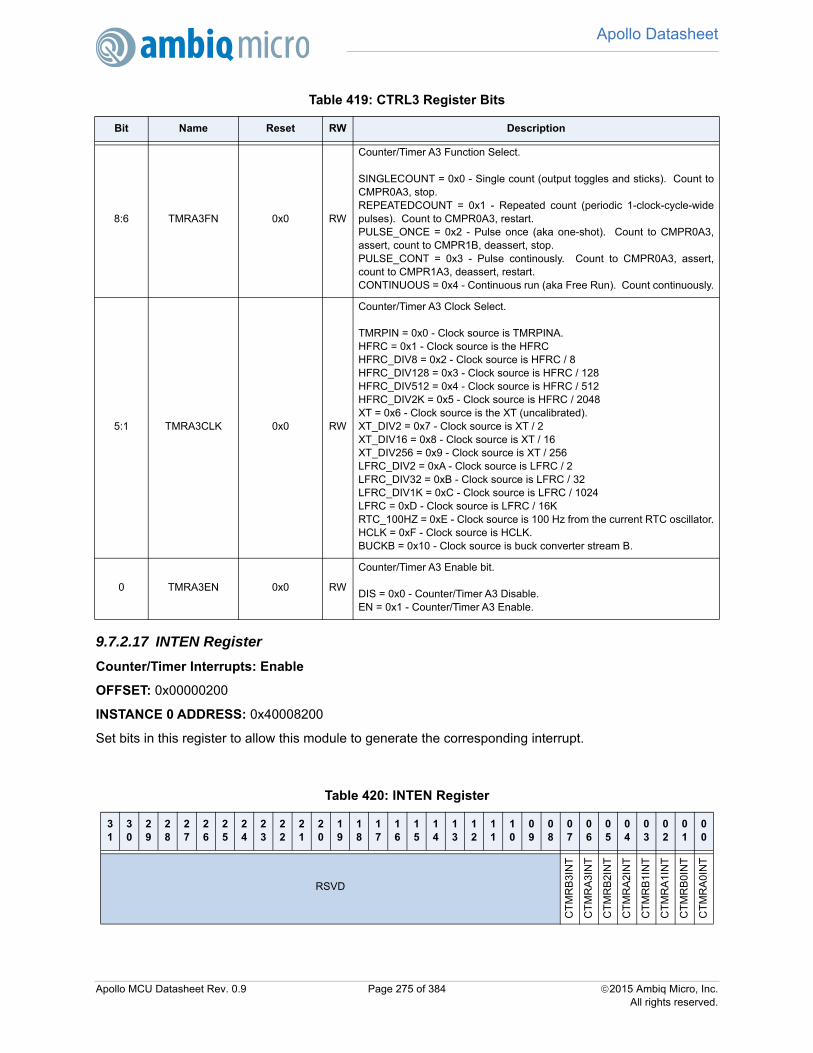
Apollo Datasheet
279
9.7.2.17 INTEN Register
Counter/Timer Interrupts: Enable
OFFSET: 0x00000200
INSTANCE 0 ADDRESS: 0x40008200
Set bits in this register to allow this module to generate the corresponding interrupt.
8:6 TMRA3FN 0x0 RW
Counter/Timer A3 Function Select.
SINGLECOUNT = 0x0 - Single count (output toggles and sticks). Count toCMPR0A3, stop.REPEATEDCOUNT = 0x1 - Repeated count (periodic 1-clock-cycle-widepulses). Count to CMPR0A3, restart.PULSE_ONCE = 0x2 - Pulse once (aka one-shot). Count to CMPR0A3,assert, count to CMPR1B, deassert, stop.PULSE_CONT = 0x3 - Pulse continously. Count to CMPR0A3, assert,count to CMPR1A3, deassert, restart.CONTINUOUS = 0x4 - Continuous run (aka Free Run). Count continuously.
5:1 TMRA3CLK 0x0 RW
Counter/Timer A3 Clock Select.
TMRPIN = 0x0 - Clock source is TMRPINA.HFRC = 0x1 - Clock source is the HFRCHFRC_DIV8 = 0x2 - Clock source is HFRC / 8HFRC_DIV128 = 0x3 - Clock source is HFRC / 128HFRC_DIV512 = 0x4 - Clock source is HFRC / 512HFRC_DIV2K = 0x5 - Clock source is HFRC / 2048XT = 0x6 - Clock source is the XT (uncalibrated).XT_DIV2 = 0x7 - Clock source is XT / 2XT_DIV16 = 0x8 - Clock source is XT / 16XT_DIV256 = 0x9 - Clock source is XT / 256LFRC_DIV2 = 0xA - Clock source is LFRC / 2LFRC_DIV32 = 0xB - Clock source is LFRC / 32LFRC_DIV1K = 0xC - Clock source is LFRC / 1024LFRC = 0xD - Clock source is LFRC / 16KRTC_100HZ = 0xE - Clock source is 100 Hz from the current RTC oscillator.HCLK = 0xF - Clock source is HCLK.BUCKB = 0x10 - Clock source is buck converter stream B.
0 TMRA3EN 0x0 RW
Counter/Timer A3 Enable bit.
DIS = 0x0 - Counter/Timer A3 Disable.EN = 0x1 - Counter/Timer A3 Enable.
Table 420: INTEN Register
31
30
29
28
27
26
25
24
23
22
21
20
19
18
17
16
15
14
13
12
11
10
09
08
07
06
05
04
03
02
01
00
RSVD
CT
MR
B3I
NT
CT
MR
A3I
NT
CT
MR
B2I
NT
CT
MR
A2I
NT
CT
MR
B1I
NT
CT
MR
A1I
NT
CT
MR
B0I
NT
CT
MR
A0I
NT
Table 419: CTRL3 Register Bits
Bit Name Reset RW Description
Apollo MCU Datasheet Rev. 0.9 Page 275 of 384 2015 Ambiq Micro, Inc.All rights reserved.

Apollo Datasheet
279
9.7.2.18 INTSTAT Register
Counter/Timer Interrupts: Status
OFFSET: 0x00000204
INSTANCE 0 ADDRESS: 0x40008204
Read bits from this register to discover the cause of a recent interrupt.
Table 421: INTEN Register Bits
Bit Name Reset RW Description
31:8 RSVD 0x0 RORESERVED
7 CTMRB3INT 0x0 RWCounter/Timer B3 interrupt.
6 CTMRA3INT 0x0 RWCounter/Timer A3 interrupt.
5 CTMRB2INT 0x0 RWCounter/Timer B2 interrupt.
4 CTMRA2INT 0x0 RWCounter/Timer A2 interrupt.
3 CTMRB1INT 0x0 RWCounter/Timer B1 interrupt.
2 CTMRA1INT 0x0 RWCounter/Timer A1 interrupt.
1 CTMRB0INT 0x0 RWCounter/Timer B0 interrupt.
0 CTMRA0INT 0x0 RWCounter/Timer A0 interrupt.
Table 422: INTSTAT Register
31
30
29
28
27
26
25
24
23
22
21
20
19
18
17
16
15
14
13
12
11
10
09
08
07
06
05
04
03
02
01
00
RSVD
CT
MR
B3I
NT
CT
MR
A3I
NT
CT
MR
B2I
NT
CT
MR
A2I
NT
CT
MR
B1I
NT
CT
MR
A1I
NT
CT
MR
B0I
NT
CT
MR
A0I
NT
Table 423: INTSTAT Register Bits
Bit Name Reset RW Description
31:8 RSVD 0x0 RORESERVED
7 CTMRB3INT 0x0 RWCounter/Timer B3 interrupt.
Apollo MCU Datasheet Rev. 0.9 Page 276 of 384 2015 Ambiq Micro, Inc.All rights reserved.

Apollo Datasheet
279
9.7.2.19 INTCLR Register
Counter/Timer Interrupts: Clear
OFFSET: 0x00000208
INSTANCE 0 ADDRESS: 0x40008208
Write a 1 to a bit in this register to clear the interrupt status associated with that bit.
6 CTMRA3INT 0x0 RWCounter/Timer A3 interrupt.
5 CTMRB2INT 0x0 RWCounter/Timer B2 interrupt.
4 CTMRA2INT 0x0 RWCounter/Timer A2 interrupt.
3 CTMRB1INT 0x0 RWCounter/Timer B1 interrupt.
2 CTMRA1INT 0x0 RWCounter/Timer A1 interrupt.
1 CTMRB0INT 0x0 RWCounter/Timer B0 interrupt.
0 CTMRA0INT 0x0 RWCounter/Timer A0 interrupt.
Table 424: INTCLR Register
31
30
29
28
27
26
25
24
23
22
21
20
19
18
17
16
15
14
13
12
11
10
09
08
07
06
05
04
03
02
01
00
RSVD
CT
MR
B3
INT
CT
MR
A3
INT
CT
MR
B2
INT
CT
MR
A2
INT
CT
MR
B1
INT
CT
MR
A1
INT
CT
MR
B0
INT
CT
MR
A0
INT
Table 425: INTCLR Register Bits
Bit Name Reset RW Description
31:8 RSVD 0x0 RORESERVED
7 CTMRB3INT 0x0 RWCounter/Timer B3 interrupt.
6 CTMRA3INT 0x0 RWCounter/Timer A3 interrupt.
5 CTMRB2INT 0x0 RWCounter/Timer B2 interrupt.
Table 423: INTSTAT Register Bits
Bit Name Reset RW Description
Apollo MCU Datasheet Rev. 0.9 Page 277 of 384 2015 Ambiq Micro, Inc.All rights reserved.

Apollo Datasheet
279
9.7.2.20 INTSET Register
Counter/Timer Interrupts: Set
OFFSET: 0x0000020C
INSTANCE 0 ADDRESS: 0x4000820C
Write a 1 to a bit in this register to instantly generate an interrupt from this module. (Generally used fortesting purposes).
4 CTMRA2INT 0x0 RWCounter/Timer A2 interrupt.
3 CTMRB1INT 0x0 RWCounter/Timer B1 interrupt.
2 CTMRA1INT 0x0 RWCounter/Timer A1 interrupt.
1 CTMRB0INT 0x0 RWCounter/Timer B0 interrupt.
0 CTMRA0INT 0x0 RWCounter/Timer A0 interrupt.
Table 426: INTSET Register
31
30
29
28
27
26
25
24
23
22
21
20
19
18
17
16
15
14
13
12
11
10
09
08
07
06
05
04
03
02
01
00
RSVD
CT
MR
B3I
NT
CT
MR
A3I
NT
CT
MR
B2I
NT
CT
MR
A2I
NT
CT
MR
B1I
NT
CT
MR
A1I
NT
CT
MR
B0I
NT
CT
MR
A0I
NT
Table 427: INTSET Register Bits
Bit Name Reset RW Description
31:8 RSVD 0x0 RORESERVED
7 CTMRB3INT 0x0 RWCounter/Timer B3 interrupt.
6 CTMRA3INT 0x0 RWCounter/Timer A3 interrupt.
5 CTMRB2INT 0x0 RWCounter/Timer B2 interrupt.
4 CTMRA2INT 0x0 RWCounter/Timer A2 interrupt.
3 CTMRB1INT 0x0 RWCounter/Timer B1 interrupt.
Table 425: INTCLR Register Bits
Bit Name Reset RW Description
Apollo MCU Datasheet Rev. 0.9 Page 278 of 384 2015 Ambiq Micro, Inc.All rights reserved.

Apollo Datasheet
279
2 CTMRA1INT 0x0 RWCounter/Timer A1 interrupt.
1 CTMRB0INT 0x0 RWCounter/Timer B0 interrupt.
0 CTMRA0INT 0x0 RWCounter/Timer A0 interrupt.
Table 427: INTSET Register Bits
Bit Name Reset RW Description
Apollo MCU Datasheet Rev. 0.9 Page 279 of 384 2015 Ambiq Micro, Inc.All rights reserved.

Apollo Datasheet
285
10. Watchdog Timer Module
Figure 46. Block diagram for the Watchdog Timer Module
10.1 Functional OverviewThe Watchdog Timer (WDT), shown in Figure 46, is used to insure that software is operational, by resettingthe Apollo MCU if the WDT reaches a configurable value before being cleared by software. The WDT isclocked by a 128 Hz clock taken from the low-power LFRC which is always active. The WDT may belocked to ensure that software cannot disable its functionality, in which case the WDTCFG register cannotbe updated. An interrupt can also be generated at a different counter value to implement an early warningfunction. Note: The RESEN bit in the WDTCFG register must be set and the WDREN bit in the RSTCFGregister must be set to enable a watchdog timer reset condition.
8-bit Counter128 Hz
8-bit Reset Value
Compare
ControlWDINT
WDRES
CLR
8-bit Interrupt Value
Compare
Apollo MCU Datasheet Rev. 0.9 Page 280 of 384 2015 Ambiq Micro, Inc.All rights reserved.

Apollo Datasheet
285
10.2 WDT RegistersWatchdog TimerINSTANCE 0 BASE ADDRESS:0x40024000
10.2.1 Register Memory Map
10.2.2 WDT Registers
10.2.2.1 CFG Register
Configuration Register
OFFSET: 0x00000000
INSTANCE 0 ADDRESS: 0x40024000
Configuration Register
Table 428: WDT Register Map
Address(s) Register Name Description
0x40024000 CFG Configuration Register
0x40024004 RSTRT Restart the watchdog timer
0x40024008 LOCK Locks the WDT
0x40024200 INTEN WDT Interrupt register: Enable
0x40024204 INTSTAT WDT Interrupt register: Status
0x40024208 INTCLR WDT Interrupt register: Clear
0x4002420C INTSET WDT Interrupt register: Set
Table 429: CFG Register
31
30
29
28
27
26
25
24
23
22
21
20
19
18
17
16
15
14
13
12
11
10
09
08
07
06
05
04
03
02
01
00
RSVD INTVAL RESVAL RSVD
RE
SE
N
INT
EN
WD
TE
N
Table 430: CFG Register Bits
Bit Name Reset RW Description
31:24 RSVD 0x0 ROThis bitfield is reserved for future use.
23:16 INTVAL 0x0 RWThis bitfield is the compare value for counter bits 7:0 to generate a watch-dog interrupt.
Apollo MCU Datasheet Rev. 0.9 Page 281 of 384 2015 Ambiq Micro, Inc.All rights reserved.
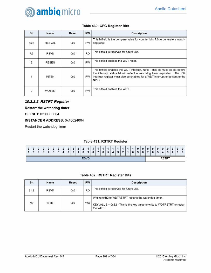
Apollo Datasheet
285
10.2.2.2 RSTRT Register
Restart the watchdog timer
OFFSET: 0x00000004
INSTANCE 0 ADDRESS: 0x40024004
Restart the watchdog timer
15:8 RESVAL 0x0 RWThis bitfield is the compare value for counter bits 7:0 to generate a watch-dog reset.
7:3 RSVD 0x0 ROThis bitfield is reserved for future use.
2 RESEN 0x0 RWThis bitfield enables the WDT reset.
1 INTEN 0x0 RW
This bitfield enables the WDT interrupt. Note : This bit must be set beforethe interrupt status bit will reflect a watchdog timer expiration. The IERinterrupt register must also be enabled for a WDT interrupt to be sent to theNVIC.
0 WDTEN 0x0 RWThis bitfield enables the WDT.
Table 431: RSTRT Register
31
30
29
28
27
26
25
24
23
22
21
20
19
18
17
16
15
14
13
12
11
10
09
08
07
06
05
04
03
02
01
00
RSVD RSTRT
Table 432: RSTRT Register Bits
Bit Name Reset RW Description
31:8 RSVD 0x0 ROThis bitfield is reserved for future use.
7:0 RSTRT 0x0 WO
Writing 0xB2 to WDTRSTRT restarts the watchdog timer.
KEYVALUE = 0xB2 - This is the key value to write to WDTRSTRT to restartthe WDT.
Table 430: CFG Register Bits
Bit Name Reset RW Description
Apollo MCU Datasheet Rev. 0.9 Page 282 of 384 2015 Ambiq Micro, Inc.All rights reserved.

Apollo Datasheet
285
10.2.2.3 LOCK RegisterLocks the WDT
OFFSET: 0x00000008
INSTANCE 0 ADDRESS: 0x40024008
Locks the WDT
10.2.2.4 INTEN Register
WDT Interrupt register: Enable
OFFSET: 0x00000200
INSTANCE 0 ADDRESS: 0x40024200
Set bits in this register to allow this module to generate the corresponding interrupt.
Table 433: LOCK Register
31
30
29
28
27
26
25
24
23
22
21
20
19
18
17
16
15
14
13
12
11
10
09
08
07
06
05
04
03
02
01
00
RSVD LOCK
Table 434: LOCK Register Bits
Bit Name Reset RW Description
31:8 RSVD 0x0 ROThis bitfield is reserved for future use.
7:0 LOCK 0x0 WO
Writing 0x3A locks the watchdog timer. Once locked, the WDTCFG reg can-not be written and WDTEN is set.
KEYVALUE = 0x3A - This is the key value to write to WDTLOCK to lock theWDT.
Table 435: INTEN Register
31
30
29
28
27
26
25
24
23
22
21
20
19
18
17
16
15
14
13
12
11
10
09
08
07
06
05
04
03
02
01
00
RSVD
WD
T
Table 436: INTEN Register Bits
Bit Name Reset RW Description
31:1 RSVD 0x0 ROThis bitfield is reserved for future use.
Apollo MCU Datasheet Rev. 0.9 Page 283 of 384 2015 Ambiq Micro, Inc.All rights reserved.

Apollo Datasheet
285
10.2.2.5 INTSTAT Register
WDT Interrupt register: Status
OFFSET: 0x00000204
INSTANCE 0 ADDRESS: 0x40024204
Read bits from this register to discover the cause of a recent interrupt.
10.2.2.6 INTCLR Register
WDT Interrupt register: Clear
OFFSET: 0x00000208
INSTANCE 0 ADDRESS: 0x40024208
Write a 1 to a bit in this register to clear the interrupt status associated with that bit.
0 WDT 0x0 RWWatchdog Timer Interrupt.
Table 437: INTSTAT Register
31
30
29
28
27
26
25
24
23
22
21
20
19
18
17
16
15
14
13
12
11
10
09
08
07
06
05
04
03
02
01
00
RSVD
WD
T
Table 438: INTSTAT Register Bits
Bit Name Reset RW Description
31:1 RSVD 0x0 ROThis bitfield is reserved for future use.
0 WDT 0x0 RWWatchdog Timer Interrupt.
Table 439: INTCLR Register
31
30
29
28
27
26
25
24
23
22
21
20
19
18
17
16
15
14
13
12
11
10
09
08
07
06
05
04
03
02
01
00
RSVD
WD
T
Table 436: INTEN Register Bits
Bit Name Reset RW Description
Apollo MCU Datasheet Rev. 0.9 Page 284 of 384 2015 Ambiq Micro, Inc.All rights reserved.

Apollo Datasheet
285
10.2.2.7 INTSET Register
WDT Interrupt register: Set
OFFSET: 0x0000020C
INSTANCE 0 ADDRESS: 0x4002420C
Write a 1 to a bit in this register to instantly generate an interrupt from this module. (Generally used fortesting purposes).
Table 440: INTCLR Register Bits
Bit Name Reset RW Description
31:1 RSVD 0x0 ROThis bitfield is reserved for future use.
0 WDT 0x0 RWWatchdog Timer Interrupt.
Table 441: INTSET Register
31
30
29
28
27
26
25
24
23
22
21
20
19
18
17
16
15
14
13
12
11
10
09
08
07
06
05
04
03
02
01
00
RSVD
WD
T
Table 442: INTSET Register Bits
Bit Name Reset RW Description
31:1 RSVD 0x0 ROThis bitfield is reserved for future use.
0 WDT 0x0 RWWatchdog Timer Interrupt.
Apollo MCU Datasheet Rev. 0.9 Page 285 of 384 2015 Ambiq Micro, Inc.All rights reserved.

Apollo Datasheet
294
11. Reset Generator Module
Figure 47. Block diagram for the Reset Generator Module
11.1 Functional OverviewThe Reset Generator Module (RSTGEN) monitors a variety of reset signals and asserts the active lowsystem reset (SYSRESETn) accordingly. A reset causes the entire system to be re-initialized, and thecause of the most recent reset is indicated by the RSTSTAT register described in Section RSTGENRegisters.
Reset sources are described in the subsequent sections and include:
• External reset pin (RSTn)• Power-on event• Brown-out event• Software request (SYSRESETREQn)• Watchdog expiration
11.2 External Reset PinThe active-low RSTn pin can be used to generate a reset using an off-chip component (e.g., a push-button). An internal pull-up resistor in the RSTn pad enables optional floating of the RSTn pin, and a de-bounce circuit ensures that glitches on RSTn do not cause unintentional resets. The RSTn pin is notmaskable. An internal pull-down device will be active during a brownout event pulling the RSTn pin low.See Figure 48
RSTn
PORn
2.1 VBODn
SYSRESETREQn
WDTRn
SYSRESETn
1.8 VBODn
Power-on Detector
Brown-out Detector
Brown-out Detector
Apollo MCU Datasheet Rev. 0.9 Page 286 of 384 2015 Ambiq Micro, Inc.All rights reserved.

Apollo Datasheet
294
Figure 48. Block diagram of circuitry for Reset pin
11.3 Power-on EventAn integrated power-on detector monitors the supply voltage and keeps SYSRESETn asserted while VDDis below the rising power-on voltage, VPOR+ (2.05 V). When VDD rises above VPOR at initial power on, thereset module will initialize the low power analog circuitry followed by de-assertion of SYSRESETn, andnormal operation proceeds. SYSRESETn is re-asserted as soon as VDD falls below the falling power-onvoltage, VPOR- (1.75 V). The power-on reset signal, PORn, is not maskable.
11.4 Brown-out EventAn integrated brown-out detector monitors the supply voltage and signals when the voltage has fallenbelow the 2.1 V and the 1.8 V threshold. An optional reset or interrupt can be enabled when the brown-outdetector indicates the supply voltage has fallen below the 2.1 V threshold. In the event the supply voltagefalls below the 1.8 V threshold, the reset module will initiate a SYSRESETn and the 1.8VBODn, is notmaskable. A brown-out event will enable the RSTn pull-down and drive the reset pin low.
11.5 Software ResetA reset may be generated via software using the Application Interrupt and Reset Control Register (AIRCR)defined in the Cortex-M4. For additional information on the AIRCR, see the ARM document titled “Cortex-M4 Devices Generic User Guide.” The software reset request is not maskable.
11.6 Watchdog ExpirationThe Timers and Counters Module described in Section 10.1 includes a watchdog timer sub-module thatgenerates an interrupt if it has not been properly managed by software within a pre-defined time. Thewatchdog reset is maskable.
Strong
Pull
Down
RSTn
RST
Button
VDD
RSTGEN
RSTn
brownout_n
RSTn Pad IO
Apollo MCU Datasheet Rev. 0.9 Page 287 of 384 2015 Ambiq Micro, Inc.All rights reserved.

Apollo Datasheet
294
11.7 RSTGEN RegistersMCU Reset GeneratorINSTANCE 0 BASE ADDRESS:0x40000000
11.7.1 Register Memory Map
11.7.2 RSTGEN Registers
11.7.3 CFG Register
Configuration Register
OFFSET: 0x00000000
INSTANCE 0 ADDRESS: 0x40000000
Configuration Register
Table 443: RSTGEN Register Map
Address(s) Register Name Description
0x40000000 CFG Configuration Register
0x40000004 SWPOI Software POI Reset
0x40000008 SWPOR Software POR Reset
0x4000000C STAT Status Register
0x40000010 CLRSTAT Clear the status register
0x40000200 INTEN Reset Interrupt register: Enable
0x40000204 INTSTAT Reset Interrupt register: Status
0x40000208 INTCLR Reset Interrupt register: Clear
0x4000020C INTSET Reset Interrupt register: Set
Table 444: CFG Register
31
30
29
28
27
26
25
24
23
22
21
20
19
18
17
16
15
14
13
12
11
10
09
08
07
06
05
04
03
02
01
00
RSVD
WD
RE
N
BO
DH
RE
N
Apollo MCU Datasheet Rev. 0.9 Page 288 of 384 2015 Ambiq Micro, Inc.All rights reserved.

Apollo Datasheet
294
11.7.3.1 SWPOI Register
Software POI Reset
OFFSET: 0x00000004
INSTANCE 0 ADDRESS: 0x40000004
Software POI Reset
Table 445: CFG Register Bits
Bit Name Reset RW Description
31:2 RSVD 0x0 RORESERVED.
1 WDREN 0x0 RWWatchdog Timer Reset Enable. NOTE: The WDT module must also be con-figured for WDT reset.
0 BODHREN 0x0 RWBrown out high (2.1v) reset enable.
Table 446: SWPOI Register
31
30
29
28
27
26
25
24
23
22
21
20
19
18
17
16
15
14
13
12
11
10
09
08
07
06
05
04
03
02
01
00
RSVD SWPOIKEY
Table 447: SWPOI Register Bits
Bit Name Reset RW Description
31:8 RSVD 0x0 RORESERVED.
7:0 SWPOIKEY 0x0 WO
0x1B generates a software POI reset.
KEYVALUE = 0x1B - Writing 0x1B key value generates a software POIreset.
Apollo MCU Datasheet Rev. 0.9 Page 289 of 384 2015 Ambiq Micro, Inc.All rights reserved.

Apollo Datasheet
294
11.7.3.2 SWPOR RegisterSoftware POR Reset
OFFSET: 0x00000008
INSTANCE 0 ADDRESS: 0x40000008
Software POR Reset
11.7.3.3 STAT Register
Status Register
OFFSET: 0x0000000C
INSTANCE 0 ADDRESS: 0x4000000C
Status Register
Table 448: SWPOR Register
31
30
29
28
27
26
25
24
23
22
21
20
19
18
17
16
15
14
13
12
11
10
09
08
07
06
05
04
03
02
01
00
RSVD SWPORKEY
Table 449: SWPOR Register Bits
Bit Name Reset RW Description
31:8 RSVD 0x0 RORESERVED.
7:0 SWPORKEY 0x0 WO
0xD4 generates a software POR reset.
KEYVALUE = 0xD4 - Writing 0xD4 key value generates a software PORreset.
Table 450: STAT Register
31
30
29
28
27
26
25
24
23
22
21
20
19
18
17
16
15
14
13
12
11
10
09
08
07
06
05
04
03
02
01
00
RSVD
WD
RS
TAT
DB
GR
STA
T
PO
IRS
TAT
SW
RS
TAT
BO
RS
TAT
PO
RS
TAT
EX
RS
TAT
Table 451: STAT Register Bits
Bit Name Reset RW Description
31:7 RSVD 0x0 RORESERVED.
Apollo MCU Datasheet Rev. 0.9 Page 290 of 384 2015 Ambiq Micro, Inc.All rights reserved.

Apollo Datasheet
294
11.7.3.4 CLRSTAT Register
Clear the status register
OFFSET: 0x00000010
INSTANCE 0 ADDRESS: 0x40000010
Clear the status register
6 WDRSTAT 0x0 ROReset was initiated by a Watchdog Timer Reset.
5 DBGRSTAT 0x0 ROReset was a initiated by Debugger Reset.
4 POIRSTAT 0x0 ROReset was a initiated by Software POI Reset.
3 SWRSTAT 0x0 ROReset was a initiated by SW POR or AIRCR Reset.
2 BORSTAT 0x0 ROReset was initiated by a Brown-Out Reset.
1 PORSTAT 0x0 ROReset was initiated by a Power-On Reset.
0 EXRSTAT 0x0 ROReset was initiated by an External Reset.
Table 452: CLRSTAT Register
31
30
29
28
27
26
25
24
23
22
21
20
19
18
17
16
15
14
13
12
11
10
09
08
07
06
05
04
03
02
01
00
RSVD
CLR
STA
T
Table 453: CLRSTAT Register Bits
Bit Name Reset RW Description
31:1 RSVD 0x0 RORESERVED.
0 CLRSTAT 0x0 WOWriting a 1 to this bit clears all bits in the RST_STAT.
Table 451: STAT Register Bits
Bit Name Reset RW Description
Apollo MCU Datasheet Rev. 0.9 Page 291 of 384 2015 Ambiq Micro, Inc.All rights reserved.

Apollo Datasheet
294
11.7.3.5 INTEN RegisterReset Interrupt register: Enable
OFFSET: 0x00000200
INSTANCE 0 ADDRESS: 0x40000200
Set bits in this register to allow this module to generate the corresponding interrupt.
11.7.3.6 INTSTAT Register
Reset Interrupt register: Status
OFFSET: 0x00000204
INSTANCE 0 ADDRESS: 0x40000204
Read bits from this register to discover the cause of a recent interrupt.
Table 454: INTEN Register
31
30
29
28
27
26
25
24
23
22
21
20
19
18
17
16
15
14
13
12
11
10
09
08
07
06
05
04
03
02
01
00
RSVD
BO
DH
Table 455: INTEN Register Bits
Bit Name Reset RW Description
31:1 RSVD 0x0 RORESERVED.
0 BODH 0x0 RWEnables an interrupt that triggers when VCC is below BODH level.
Table 456: INTSTAT Register
31
30
29
28
27
26
25
24
23
22
21
20
19
18
17
16
15
14
13
12
11
10
09
08
07
06
05
04
03
02
01
00
RSVD
BO
DH
Table 457: INTSTAT Register Bits
Bit Name Reset RW Description
31:1 RSVD 0x0 RORESERVED.
Apollo MCU Datasheet Rev. 0.9 Page 292 of 384 2015 Ambiq Micro, Inc.All rights reserved.

Apollo Datasheet
294
11.7.3.7 INTCLR Register
Reset Interrupt register: Clear
OFFSET: 0x00000208
INSTANCE 0 ADDRESS: 0x40000208
Write a 1 to a bit in this register to clear the interrupt status associated with that bit.
11.7.3.8 INTSET Register
Reset Interrupt register: Set
OFFSET: 0x0000020C
INSTANCE 0 ADDRESS: 0x4000020C
Write a 1 to a bit in this register to instantly generate an interrupt from this module. (Generally used fortesting purposes).
0 BODH 0x0 RWEnables an interrupt that triggers when VCC is below BODH level.
Table 458: INTCLR Register
31
30
29
28
27
26
25
24
23
22
21
20
19
18
17
16
15
14
13
12
11
10
09
08
07
06
05
04
03
02
01
00
RSVD
BO
DH
Table 459: INTCLR Register Bits
Bit Name Reset RW Description
31:1 RSVD 0x0 RORESERVED.
0 BODH 0x0 RWEnables an interrupt that triggers when VCC is below BODH level.
Table 460: INTSET Register
31
30
29
28
27
26
25
24
23
22
21
20
19
18
17
16
15
14
13
12
11
10
09
08
07
06
05
04
03
02
01
00
RSVD
BO
DH
Table 457: INTSTAT Register Bits
Bit Name Reset RW Description
Apollo MCU Datasheet Rev. 0.9 Page 293 of 384 2015 Ambiq Micro, Inc.All rights reserved.

Apollo Datasheet
294
Table 461: INTSET Register Bits
Bit Name Reset RW Description
31:1 RSVD 0x0 RORESERVED.
0 BODH 0x0 RWEnables an interrupt that triggers when VCC is below BODH level.
Apollo MCU Datasheet Rev. 0.9 Page 294 of 384 2015 Ambiq Micro, Inc.All rights reserved.

Apollo Datasheet
308
12. UART Module
Figure 49. Block Diagram for the UART Module
12.1 FeaturesThe UART Module includes the following key features:
• Operates independently, allowing the MCU to enter a low power sleep mode during commu-nication
• 32 x 8 transmit FIFO and 32 x 12 receive FIFO to reduce MCU computational load• Programmable baud rate generator capable of a maximum rate of 921,600 bits per second• Fully programmable data size, parity, and stop bit length• Programmable hardware flow control• Support for full-duplex and half-duplex communication• Loopback functionality for diagnostics and testing
12.2 Functional OverviewShown in Figure 49, the UART Module converts parallel data written through the APB Slave port into serialdata which is transmitted to an external device. It also receives serial data from an external device andconverts it to parallel data, which is then stored in a buffer until the CPU reads the data.
The UART Module includes a programmable baud rate generator which is capable of operating at amaximum of 921,600 bits per second. An interrupt generator will optionally send interrupts to the CPU corefor transmit, receive and error events.
Internally, the UART Module maintains two FIFOs. The transmit FIFO is 1-byte wide with 32 locations. Thereceive FIFO is 12-bits wide with 32 locations. The extra four bits in the receive FIFO are used to captureany error status information that the MCU needs to analyze.
APB
UART TX
UART RX
IRQ
APB
Slave
Transmit
FIFO
Register
Block
Receive
FIFO
Interrupt
Generation
Transmit
Interface
Receive
Interface
Apollo MCU Datasheet Rev. 0.9 Page 295 of 384 2015 Ambiq Micro, Inc.All rights reserved.

Apollo Datasheet
308
Clocking to the UART serial logic is generated by a dedicated UARTCLK from the Clock GeneratorModule. The frequency of this clock is determined by the desired baud rate. For maximum baud rates, thisclock would be clocked at the 24 MHz maximum as generated by the HFRC.The major functional blocks of the UART are discussed briefly in the subsequent sections.
12.3 Enabling and Selecting the UART ClockBefore the UART Module can communicate, a clock frequency must be selected for the UART clock, andthe clock must then be enabled. Use the UART_CR register to select the desired clock frequency, FUART.After selecting the desired frequency, enable the UART clock using the CLK_GEN_UARTEN register.Unlike other modules that automatically turn off their clock sources automatically, the UART clock must bemanually disabled using the aforementioned CLK_GEN_UARTEN register. To ensure minimum energyoperation, the UART clock should be enabled for the minimum time possible and should be disabled assoon as UART communication is complete.
12.4 ConfigurationThe UART Register Block in Figure 49 may be set to configure the UART Module. The data width, numberof stop bits, and parity may all be configured using the UART_LCRH register.
The baud rate is configured using the integer UART_IBRD and UART_FBRD registers. The correct valuesfor UART_IBRD and UART_FBRD may be determined according to the following equation:
FUART/(16·BR) = IBRD + FBRD
FUART is the frequency of the UART clock. BR is the desired baud rate. IBRD is the integer portion of thebaud rate divisor. FBRD is the fractional portion of the baud rate divisor.
The UART Module supports independent CTS and RTS hardware flow control. All flow controlconfiguration may be set using the UART_CR register.
12.5 Transmit FIFO and Receive FIFOThe transmit and receive FIFOs may both be accessed via the same 8-bit word in the UART_DR register.The transmit FIFO stores up to 32 8-bit words and can be written using writes to UART_DR. The receiveFIFO stores up to 32 12-bit words and can be read using reads to UART_DR. Note that each 12-bit receiveFIFO word includes an 8-bit data word and a 4-bit error status word.
Apollo MCU Datasheet Rev. 0.9 Page 296 of 384 2015 Ambiq Micro, Inc.All rights reserved.

Apollo Datasheet
308
12.6 UART RegistersSerial UARTINSTANCE 0 BASE ADDRESS:0x4001C000
12.6.1 Register Memory Map
12.6.2 UART Registers
12.6.2.1 DR Register
UART Data Register
OFFSET: 0x00000000
INSTANCE 0 ADDRESS: 0x4001C000
UART Data Register
Table 462: UART Register Map
Address(s) Register Name Description
0x4001C000 DR UART Data Register
0x4001C004 RSR UART Status Register
0x4001C018 FR Flag Register
0x4001C020 ILPR IrDA Counter
0x4001C024 IBRD Integer Baud Rate Divisor
0x4001C028 FBRD Fractional Baud Rate Divisor
0x4001C02C LCRH Line Control High
0x4001C030 CR Control Register
0x4001C034 IFLS FIFO Interrupt Level Select
0x4001C038 IER Interrupt Enable
0x4001C03C IES Interrupt Status
0x4001C040 MIS Masked Interrupt Status
0x4001C044 IEC Interrupt Clear
Table 463: DR Register
31
30
29
28
27
26
25
24
23
22
21
20
19
18
17
16
15
14
13
12
11
10
09
08
07
06
05
04
03
02
01
00
RSVD
OE
DA
TA
BE
DA
TA
PE
DA
TA
FE
DA
TA
DATA
Apollo MCU Datasheet Rev. 0.9 Page 297 of 384 2015 Ambiq Micro, Inc.All rights reserved.

Apollo Datasheet
308
12.6.2.2 RSR Register
UART Status Register
OFFSET: 0x00000004
INSTANCE 0 ADDRESS: 0x4001C004
UART Status Register
Table 464: DR Register Bits
Bit Name Reset RW Description
31:12 RSVD 0x0 ROThis bitfield is reserved for future use.
11 OEDATA 0x0 RO
This is the overrun error indicator.
NOERR = 0x0 - No error on UART OEDATA, overrun error indicator.ERR = 0x1 - Error on UART OEDATA, overrun error indicator.
10 BEDATA 0x0 RO
This is the break error indicator.
NOERR = 0x0 - No error on UART BEDATA, break error indicator.ERR = 0x1 - Error on UART BEDATA, break error indicator.
9 PEDATA 0x0 RO
This is the parity error indicator.
NOERR = 0x0 - No error on UART PEDATA, parity error indicator.ERR = 0x1 - Error on UART PEDATA, parity error indicator.
8 FEDATA 0x0 RO
This is the framing error indicator.
NOERR = 0x0 - No error on UART FEDATA, framing error indicator.ERR = 0x1 - Error on UART FEDATA, framing error indicator.
7:0 DATA 0x0 RWThis is the UART data port.
Table 465: RSR Register
31
30
29
28
27
26
25
24
23
22
21
20
19
18
17
16
15
14
13
12
11
10
09
08
07
06
05
04
03
02
01
00
RSVD
OE
STA
T
BE
STA
T
PE
STA
T
FE
STA
T
Table 466: RSR Register Bits
Bit Name Reset RW Description
31:4 RSVD 0x0 ROThis bitfield is reserved for future use.
Apollo MCU Datasheet Rev. 0.9 Page 298 of 384 2015 Ambiq Micro, Inc.All rights reserved.

Apollo Datasheet
308
12.6.2.3 FR Register
Flag Register
OFFSET: 0x00000018
INSTANCE 0 ADDRESS: 0x4001C018
Flag Register
3 OESTAT 0x0 RW
This is the overrun error indicator.
NOERR = 0x0 - No error on UART OESTAT, overrun error indicator.ERR = 0x1 - Error on UART OESTAT, overrun error indicator.
2 BESTAT 0x0 RW
This is the break error indicator.
NOERR = 0x0 - No error on UART BESTAT, break error indicator.ERR = 0x1 - Error on UART BESTAT, break error indicator.
1 PESTAT 0x0 RW
This is the parity error indicator.
NOERR = 0x0 - No error on UART PESTAT, parity error indicator.ERR = 0x1 - Error on UART PESTAT, parity error indicator.
0 FESTAT 0x0 RW
This is the framing error indicator.
NOERR = 0x0 - No error on UART FESTAT, framing error indicator.ERR = 0x1 - Error on UART FESTAT, framing error indicator.
Table 467: FR Register
31
30
29
28
27
26
25
24
23
22
21
20
19
18
17
16
15
14
13
12
11
10
09
08
07
06
05
04
03
02
01
00
RSVD RI
TX
FE
RX
FF
TX
FF
RX
FE
BU
SY
DC
D
DS
R
CT
STable 468: FR Register Bits
Bit Name Reset RW Description
31:9 RSVD 0x0 ROThis bitfield is reserved for future use.
8 RI 0x0 ROThis bit holds the ring indicator.
7 TXFE 0x0 ROThis bit holds the transmit FIFO empty indicator.
XMTFIFO_EMPTY = 0x1 - Transmit fifo is empty.
6 RXFF 0x0 ROThis bit holds the receive FIFO full indicator.
RCVFIFO_FULL = 0x1 - Receive fifo is full.
Table 466: RSR Register Bits
Bit Name Reset RW Description
Apollo MCU Datasheet Rev. 0.9 Page 299 of 384 2015 Ambiq Micro, Inc.All rights reserved.

Apollo Datasheet
308
12.6.2.4 ILPR Register
IrDA Counter
OFFSET: 0x00000020
INSTANCE 0 ADDRESS: 0x4001C020
IrDA Counter
5 TXFF 0x0 ROThis bit holds the transmit FIFO full indicator.
XMTFIFO_FULL = 0x1 - Transmit fifo is full.
4 RXFE 0x0 ROThis bit holds the receive FIFO empty indicator.
RCVFIFO_EMPTY = 0x1 - Receive fifo is empty.
3 BUSY 0x0 ROThis bit holds the busy indicator.
BUSY = 0x1 - UART busy indicator.
2 DCD 0x0 ROThis bit holds the data carrier detect indicator.
DETECTED = 0x1 - Data carrier detect detected.
1 DSR 0x0 ROThis bit holds the data set ready indicator.
READY = 0x1 - Data set ready.
0 CTS 0x0 ROThis bit holds the clear to send indicator.
CLEARTOSEND = 0x1 - Clear to send is indicated.
Table 469: ILPR Register
31
30
29
28
27
26
25
24
23
22
21
20
19
18
17
16
15
14
13
12
11
10
09
08
07
06
05
04
03
02
01
00
RSVD ILPDVSR
Table 470: ILPR Register Bits
Bit Name Reset RW Description
31:8 RSVD 0x0 ROThis bitfield is reserved for future use.
7:0 ILPDVSR 0x0 RWThese bits hold the IrDA counter divisor.
Table 468: FR Register Bits
Bit Name Reset RW Description
Apollo MCU Datasheet Rev. 0.9 Page 300 of 384 2015 Ambiq Micro, Inc.All rights reserved.

Apollo Datasheet
308
12.6.2.5 IBRD RegisterInteger Baud Rate Divisor
OFFSET: 0x00000024
INSTANCE 0 ADDRESS: 0x4001C024
Integer Baud Rate Divisor
12.6.2.6 FBRD Register
Fractional Baud Rate Divisor
OFFSET: 0x00000028
INSTANCE 0 ADDRESS: 0x4001C028
Fractional Baud Rate Divisor
Table 471: IBRD Register
31
30
29
28
27
26
25
24
23
22
21
20
19
18
17
16
15
14
13
12
11
10
09
08
07
06
05
04
03
02
01
00
RSVD DIVINT
Table 472: IBRD Register Bits
Bit Name Reset RW Description
31:16 RSVD 0x0 ROThis bitfield is reserved for future use.
15:0 DIVINT 0x0 RWThese bits hold the baud integer divisor.
Table 473: FBRD Register
31
30
29
28
27
26
25
24
23
22
21
20
19
18
17
16
15
14
13
12
11
10
09
08
07
06
05
04
03
02
01
00
RSVD DIVFRAC
Table 474: FBRD Register Bits
Bit Name Reset RW Description
31:6 RSVD 0x0 ROThis bitfield is reserved for future use.
5:0 DIVFRAC 0x0 RWThese bits hold the baud fractional divisor.
Apollo MCU Datasheet Rev. 0.9 Page 301 of 384 2015 Ambiq Micro, Inc.All rights reserved.

Apollo Datasheet
308
12.6.2.7 LCRH RegisterLine Control High
OFFSET: 0x0000002C
INSTANCE 0 ADDRESS: 0x4001C02C
Line Control High
Table 475: LCRH Register
31
30
29
28
27
26
25
24
23
22
21
20
19
18
17
16
15
14
13
12
11
10
09
08
07
06
05
04
03
02
01
00
RSVD
SP
S
WLE
N
FE
N
ST
P2
EP
S
PE
N
BR
K
Table 476: LCRH Register Bits
Bit Name Reset RW Description
31:8 RSVD 0x0 ROThis bitfield is reserved for future use.
7 SPS 0x0 RWThis bit holds the stick parity select.
6:5 WLEN 0x0 RWThese bits hold the write length.
4 FEN 0x0 RWThis bit holds the FIFO enable.
3 STP2 0x0 RWThis bit holds the two stop bits select.
2 EPS 0x0 RWThis bit holds the even parity select.
1 PEN 0x0 RWThis bit holds the parity enable.
0 BRK 0x0 RWThis bit holds the break set.
Apollo MCU Datasheet Rev. 0.9 Page 302 of 384 2015 Ambiq Micro, Inc.All rights reserved.

Apollo Datasheet
308
12.6.2.8 CR RegisterControl Register
OFFSET: 0x00000030
INSTANCE 0 ADDRESS: 0x4001C030
Control Register
Table 477: CR Register
31
30
29
28
27
26
25
24
23
22
21
20
19
18
17
16
15
14
13
12
11
10
09
08
07
06
05
04
03
02
01
00
RSVD
CT
SE
N
RT
SE
N
OU
T2
OU
T1
RT
S
DT
R
RX
E
TX
E
LB
E
CLK
SE
L
CL
KE
N
SIR
LP
SIR
EN
UA
RT
EN
Table 478: CR Register Bits
Bit Name Reset RW Description
31:16 RSVD 0x0 ROThis bitfield is reserved for future use.
15 CTSEN 0x0 RWThis bit enables CTS hardware flow control.
14 RTSEN 0x0 RWThis bit enables RTS hardware flow control.
13 OUT2 0x0 RWThis bit holds modem Out2.
12 OUT1 0x0 RWThis bit holds modem Out1.
11 RTS 0x0 RWThis bit enables request to send.
10 DTR 0x0 RWThis bit enables data transmit ready.
9 RXE 0x1 RWThis bit is the receive enable.
8 TXE 0x1 RWThis bit is the transmit enable.
7 LBE 0x0 RWThis bit is the loopback enable.
Apollo MCU Datasheet Rev. 0.9 Page 303 of 384 2015 Ambiq Micro, Inc.All rights reserved.

Apollo Datasheet
308
12.6.2.9 IFLS Register
FIFO Interrupt Level Select
OFFSET: 0x00000034
INSTANCE 0 ADDRESS: 0x4001C034
FIFO Interrupt Level Select
6:4 CLKSEL 0x0 RW
This bitfield is the UART clock select.
NOCLK = 0x0 - No UART clock. This is the low power default.24MHZ = 0x1 - 24 MHz clock. Must be used if CLKGEN CORESEL=0.12MHZ = 0x2 - 12 MHz clock. Must be used if CLKGEN CORESEL=1. Notethat CORESEL=1 is unsupported by the IO Master.6MHZ = 0x3 - 6 MHz clock. Must be used if CLKGEN CORESEL=2, 3, or 4.Note that CORESEL=2 is unsupported.3MHZ = 0x4 - 3 MHz clock. Must be used if CLKGEN CORESEL=5, 6, or 7.RSVD5 = 0x5 - Reserved.RSVD6 = 0x6 - Reserved.RSVD7 = 0x7 - Reserved.
3 CLKEN 0x0 RWThis bit is the UART clock enable.
2 SIRLP 0x0 RWThis bit is the SIR low power select.
1 SIREN 0x0 RWThis bit is the SIR ENDEC enable.
0 UARTEN 0x0 RWThis bit is the UART enable.
Table 479: IFLS Register
31
30
29
28
27
26
25
24
23
22
21
20
19
18
17
16
15
14
13
12
11
10
09
08
07
06
05
04
03
02
01
00
RSVD
RX
IFLS
EL
TX
IFLS
EL
Table 480: IFLS Register Bits
Bit Name Reset RW Description
31:6 RSVD 0x0 ROThis bitfield is reserved for future use.
5:3 RXIFLSEL 0x2 RWThese bits hold the receive FIFO interrupt level.
2:0 TXIFLSEL 0x2 RWThese bits hold the transmit FIFO interrupt level.
Table 478: CR Register Bits
Bit Name Reset RW Description
Apollo MCU Datasheet Rev. 0.9 Page 304 of 384 2015 Ambiq Micro, Inc.All rights reserved.

Apollo Datasheet
308
12.6.2.10 IER RegisterInterrupt Enable
OFFSET: 0x00000038
INSTANCE 0 ADDRESS: 0x4001C038
Interrupt Enable
Table 481: IER Register
31
30
29
28
27
26
25
24
23
22
21
20
19
18
17
16
15
14
13
12
11
10
09
08
07
06
05
04
03
02
01
00
RSVD
OE
IM
BE
IM
PE
IM
FE
IM
RT
IM
TX
IM
RX
IM
DS
RM
IM
DC
DM
IM
CT
SM
IM
RIM
IM
Table 482: IER Register Bits
Bit Name Reset RW Description
31:11 RSVD 0x0 ROThis bitfield is reserved for future use.
10 OEIM 0x0 RWThis bit holds the overflow interrupt enable.
9 BEIM 0x0 RWThis bit holds the break error interrupt enable.
8 PEIM 0x0 RWThis bit holds the parity error interrupt enable.
7 FEIM 0x0 RWThis bit holds the framing error interrupt enable.
6 RTIM 0x0 RWThis bit holds the receive timeout interrupt enable.
5 TXIM 0x0 RWThis bit holds the transmit interrupt enable.
4 RXIM 0x0 RWThis bit holds the receive interrupt enable.
3 DSRMIM 0x0 RWThis bit holds the modem DSR interrupt enable.
2 DCDMIM 0x0 RWThis bit holds the modem DCD interrupt enable.
1 CTSMIM 0x0 RWThis bit holds the modem CTS interrupt enable.
0 RIMIM 0x0 RWThis bit holds the modem RI interrupt enable.
Apollo MCU Datasheet Rev. 0.9 Page 305 of 384 2015 Ambiq Micro, Inc.All rights reserved.

Apollo Datasheet
308
12.6.2.11 IES RegisterInterrupt Status
OFFSET: 0x0000003C
INSTANCE 0 ADDRESS: 0x4001C03C
Interrupt Status
Table 483: IES Register
31
30
29
28
27
26
25
24
23
22
21
20
19
18
17
16
15
14
13
12
11
10
09
08
07
06
05
04
03
02
01
00
RSVD
OE
RIS
BE
RIS
PE
RIS
FE
RIS
RT
RIS
TX
RIS
RX
RIS
DS
RM
RIS
DC
DM
RIS
CT
SM
RIS
RIM
RIS
Table 484: IES Register Bits
Bit Name Reset RW Description
31:11 RSVD 0x0 ROThis bitfield is reserved for future use.
10 OERIS 0x0 ROThis bit holds the overflow interrupt status.
9 BERIS 0x0 ROThis bit holds the break error interrupt status.
8 PERIS 0x0 ROThis bit holds the parity error interrupt status.
7 FERIS 0x0 ROThis bit holds the framing error interrupt status.
6 RTRIS 0x0 ROThis bit holds the receive timeout interrupt status.
5 TXRIS 0x0 ROThis bit holds the transmit interrupt status.
4 RXRIS 0x0 ROThis bit holds the receive interrupt status.
3 DSRMRIS 0x0 ROThis bit holds the modem DSR interrupt status.
2 DCDMRIS 0x0 ROThis bit holds the modem DCD interrupt status.
1 CTSMRIS 0x0 ROThis bit holds the modem CTS interrupt status.
0 RIMRIS 0x0 ROThis bit holds the modem RI interrupt status.
Apollo MCU Datasheet Rev. 0.9 Page 306 of 384 2015 Ambiq Micro, Inc.All rights reserved.

Apollo Datasheet
308
12.6.2.12 MIS RegisterMasked Interrupt Status
OFFSET: 0x00000040
INSTANCE 0 ADDRESS: 0x4001C040
Masked Interrupt Status
Table 485: MIS Register
31
30
29
28
27
26
25
24
23
22
21
20
19
18
17
16
15
14
13
12
11
10
09
08
07
06
05
04
03
02
01
00
RSVD
OE
MIS
BE
MIS
PE
MIS
FE
MIS
RT
MIS
TX
MIS
RX
MIS
DS
RM
MIS
DC
DM
MIS
CT
SM
MIS
RIM
MIS
Table 486: MIS Register Bits
Bit Name Reset RW Description
31:11 RSVD 0x0 ROThis bitfield is reserved for future use.
10 OEMIS 0x0 ROThis bit holds the overflow interrupt status masked.
9 BEMIS 0x0 ROThis bit holds the break error interrupt status masked.
8 PEMIS 0x0 ROThis bit holds the parity error interrupt status masked.
7 FEMIS 0x0 ROThis bit holds the framing error interrupt status masked.
6 RTMIS 0x0 ROThis bit holds the receive timeout interrupt status masked.
5 TXMIS 0x0 ROThis bit holds the transmit interrupt status masked.
4 RXMIS 0x0 ROThis bit holds the receive interrupt status masked.
3 DSRMMIS 0x0 ROThis bit holds the modem DSR interrupt status masked.
2 DCDMMIS 0x0 ROThis bit holds the modem DCD interrupt status masked.
1 CTSMMIS 0x0 ROThis bit holds the modem CTS interrupt status masked.
0 RIMMIS 0x0 ROThis bit holds the modem RI interrupt status masked.
Apollo MCU Datasheet Rev. 0.9 Page 307 of 384 2015 Ambiq Micro, Inc.All rights reserved.

Apollo Datasheet
308
12.6.2.13 IEC RegisterInterrupt Clear
OFFSET: 0x00000044
INSTANCE 0 ADDRESS: 0x4001C044
Interrupt Clear
Table 487: IEC Register
31
30
29
28
27
26
25
24
23
22
21
20
19
18
17
16
15
14
13
12
11
10
09
08
07
06
05
04
03
02
01
00
RSVD
OE
IC
BE
IC
PE
IC
FE
IC
RT
IC
TX
IC
RX
IC
DS
RM
IC
DC
DM
IC
CT
SM
IC
RIM
IC
Table 488: IEC Register Bits
Bit Name Reset RW Description
31:11 RSVD 0x0 ROThis bitfield is reserved for future use.
10 OEIC 0x0 WOThis bit holds the overflow interrupt clear.
9 BEIC 0x0 WOThis bit holds the break error interrupt clear.
8 PEIC 0x0 WOThis bit holds the parity error interrupt clear.
7 FEIC 0x0 WOThis bit holds the framing error interrupt clear.
6 RTIC 0x0 WOThis bit holds the receive timeout interrupt clear.
5 TXIC 0x0 WOThis bit holds the transmit interrupt clear.
4 RXIC 0x0 WOThis bit holds the receive interrupt clear.
3 DSRMIC 0x0 WOThis bit holds the modem DSR interrupt clear.
2 DCDMIC 0x0 WOThis bit holds the modem DCD interrupt clear.
1 CTSMIC 0x0 WOThis bit holds the modem CTS interrupt clear.
0 RIMIC 0x0 WOThis bit holds the modem RI interrupt clear.
Apollo MCU Datasheet Rev. 0.9 Page 308 of 384 2015 Ambiq Micro, Inc.All rights reserved.

Apollo Datasheet
343
13. ADC and Temperature Sensor Module
Figure 50. Block Diagram for ADC and Temperature Sensor
13.1 FeaturesThe Analog to Digital Converter (ADC) and Temperature Sensor Module includes a single-ended 10-bitmulti-channel Successive Approximation Register (SAR) ADC as shown in Figure 50.
Key features include:
13 user-selectable channels including: - external pins- internal voltages- voltage divider- temperature sensor
User-selectable on-chip and off-chip reference voltages Single shot, repeating single shot, scan, and repeating scan modes User-selectable clock source for variable sampling rates User-selectable track/hold time Multiple conversion triggers including external pins, a timer, and a software write Automatically accumulate and scale module for hardware averaging of samples An 8-entry FIFO for storing measurement results and maximizing MCU sleep time Window comparator for monitoring voltages excursions into or out of user-selectable thresholds Multiple low power modes between conversions Up to 800 kSps sampling rate
SAR ADC
ADC_I0
ADC_I1
SWT
...
ADC_TT
ADC_ET0
ADC_ET1Mode
Controller
VDD
VREFINTADC_REF
Bandgap Ref
ADC_I7
VDD
VSS
ADC_ET7
...
Accu
mu
late
an
d S
cale
Window
Comparator
......
Temp Sensor
TRIGINT
VIN
ADC_CLKHFRC Osc Divider
SLOT0
SLOT1
SLOT2
SLOT3
SLOT4
SLOT5
SLOT6
SLOT7
8
deep
FIFODivider &Batt. Load
Apollo MCU Datasheet Rev. 0.9 Page 309 of 384 2015 Ambiq Micro, Inc.All rights reserved.

Apollo Datasheet
343
13.2 Functional OverviewThe Apollo MCU integrates a sophisticated Analog to Digital Converter (ADC) block for sensing bothinternal and external voltages. The block provides eight separately managed conversion requests, calledslots. The result of each conversion requests is delivered to an eight deep FIFO. Firmware can utilizevarious interrupt notifications to determine when to collect the sampled data from the FIFO. This block isextremely effective at automatically managing its power states and its clock sources.13.2.1 Clock Source and Dividers
The ADC runs off of the HFRC clock source. When the ADC block is enabled, it requests an HFRC clocksource. There is an automatic hardware hand shake between the clock generator and the ADC. If the ADCis the only block requesting an HFRC based clock then the HFRC will be automatically started. The ADCcan select one of the following clock divisions from the 24MHz HFRC:
12MHz 6MHz 3MHz 1.5MHz
13.2.2 13 Channel Analog Mux
As shown in Figure 50, the ADC block contains a 13 channel analog multiplexer on the input port to theanalog to digital converter. Eight of the GPIO pins on the Apollo MCU can be selected as analog inputs tothe ADC through a combination of settings in the PAD configuration registers in the GPIO block andsettings in the configuration registers described below.
The analog mux channels are connected as follows:
ADC_EXT0 external GPIO pin connection. ADC_EXT1 external GPIO pin connection. ADC_EXT2 external GPIO pin connection. ADC_EXT3 external GPIO pin connection. ADC_EXT4 external GPIO pin connection. ADC_EXT5 external GPIO pin connection. ADC_EXT6 external GPIO pin connection. ADC_EXT7 external GPIO pin connection. ADC_TEMP internal temperature sensor. ADC_VSS internal ground connection. ADC_VDD internal connection to input power rails. ADC_DIV3 internal voltage divide by 3 connection to the input power rail. ADC_DIV3_LOAD internal voltage divide by 3 connection to input power rail with the 500 ohm load resis-
tor turned on.
Refer to the detailed register information below for the exact coding of the channel selection bit field. Alsothe use of the voltage divider and switchable load resistor are detailed below. See “Voltage Divider andSwitchable Battery Load” on page 319.
13.2.3 Triggering and Trigger Sources
The ADC block can be initially triggered from one of eight sources. Once triggered, it can be repetitivelytriggered from counter/timer number three. Seven of the GPIO pins on the Apollo MCU can be selected astrigger inputs to the ADC through a combination of settings in the PAD configuration registers in the GPIOblock and settings in SLOT configuration registers described below. Initial trigger sources are as follows:
1. ADC_TRIG0 external GPIO pin connection.
2. ADC_TRIG1 external GPIO pin connection.
Apollo MCU Datasheet Rev. 0.9 Page 310 of 384 2015 Ambiq Micro, Inc.All rights reserved.

Apollo Datasheet
343
3. ADC_TRIG2 external GPIO pin connection.4. ADC_TRIG3 external GPIO pin connection.
5. ADC_TRIG5 external GPIO pin connection.
6. ADC_TRIG6 external GPIO pin connection.
7. ADC_TRIG7 external GPIO pin connection.
8. ADC_SWT software trigger.
Refer to the ADC Configuration Register in the detailed register information section below. The initialtrigger source is selected in the TRIGSEL field, as shown below. In addition, one can select a triggerpolarity in this register. A large number of GPIO pin trigger sources are provided to allow pin configurationflexibility at the system definition and board layout phases of development.
The software trigger is effected by writing 0x37 to the software trigger register in the ADC block. Note thatit must be selected as the trigger source before writing to this register will cause an actual trigger event.
The discussion of the use of counter/timer three as a source for repetitive triggering is deferred until later inthis chapter. See “Repeat Mode” on page 317.
Finally it is important to note that a trigger event applies to all enabled slots as a whole. Individual slots cannot be separately triggered.
13.2.4 Voltage Reference Sources
The Apollo MCU allows one of three reference sources to be used for the analog to digital conversion step:
Bandgap Reference Source VDD internal voltage rail External reference via GPIO16
13.2.5 Eight Automatically Managed Conversion Slots
If the SAR is the heart of the ADC block, then the conversion SLOTs and their mode controller are thebrains of this block. The ADC block contains eight conversion slot control registers, one for each of theeight slots. These can be thought of as time slots in the conversion process. When a slot is enabled, itparticipates in a conversion cycle. The ADC’s mode controller cycles through up to eight time slots eachtime it is triggered. For each slot that is enabled, a conversion cycle is performed based on the settings inthe slot configuration register for that slot. Slots are enabled when the LSB of the slot configuration is set toone. See “One SLOT Configuration Register” on page 311.
The window comparator enable will be discussed in a subsequent section, below. See “WindowComparator” on page 314. The number of samples to accumulate will also be explained in a subsequentsection. See “Automatic Sample Accumulation and Scaling” on page 312.
Table 489: One SLOT Configuration Register
31
30
29
28
27
26
25
24
23
22
21
20
19
18
17
16
15
14
13
12
11
10
09
08
07
06
05
04
03
02
01
00
Reserved
#Samples
to Accum.
ReservedTRACK &
HOLDReserved
CHANNEL SELECT
Reserved
WIN
DO
W_C
OM
P
SLO
T_E
NA
BLE
Apollo MCU Datasheet Rev. 0.9 Page 311 of 384 2015 Ambiq Micro, Inc.All rights reserved.

Apollo Datasheet
343
As described above, the channel select bit field specifies which one of the analog multiplexer channels willbe used for the conversions requested for an individual slot. See “13 Channel Analog Mux” on page 310.As its name implies, the track and hold bit field controls the time from when an analog mux channel isselected until the ADC hold circuit captures the analog value on that input. Refer to the detailed registersection for the specifics of programming this bit field, but the bit field essentially offers powers of twoincreasing hold times from 1 to 128 ADC clocks. Note that this track and hold time can be specifiedindependently for each of the eight conversion slots.
Each of the eight conversion slots can independently specify:
Analog Multiplexer Channel Selection Track and Hold Time Participation in Window Comparisons Automatic Sample Accumulation
13.2.6 Automatic Sample Accumulation and Scaling
The ADC block offers a facility for the automatic accumulation of samples without requiring coreinvolvement. Thus up to 128 samples per slot can be accumulated without waking the core. This facilitatesaveraging algorithms to smooth out the data samples. Each slot can request from 1 to 128 samples to beaccumulated before producing a result in the FIFO. NOTE: each slot can independently specify how manysamples to accumulate so results can enter the FIFO from different slots at different rates.
All slots write their accumulated results to the FIFO in exactly the same format regardless of how manysample were accumulated to produce the results. Table 490 shows the format that is used by allconversions. This is a scaled integer format with a 6-bit fractional part. The format for ALL results is this10.6 format.
IMPORTANT: if the accumulation control for a slot is set for one sample then the 10-bit value coming fromthe ADC will be inserted into bits 6 through 15 in this format.
Each slot contains a 17-bit accumulator as shown in Table 491, “Per Slot Sample Accumulator,” onpage 312. When the ADC is triggered for the last sample of an accumulation, the accumulator is cleared.Then when each active slot obtains a conversion from the analog side, it is added to the value in itsaccumulator.
If a slot is set to accumulate 128 samples per result then the accumulator could reach a maximum value of:
128*1023 = 128*1023 = 130944 = 217 - 128, hence the 17 bit accumulator.
Table 490: 10.6 ADC Sample Format
15
14
13
12
11
10
09
08
07
06
05
04
03
02
01
00
10-bit Integer 6-bit Fraction
Table 491: Per Slot Sample Accumulator
16
15
14
13
12
11
10
09
08
07
06
05
04
03
02
01
00
Accumulator
Apollo MCU Datasheet Rev. 0.9 Page 312 of 384 2015 Ambiq Micro, Inc.All rights reserved.

Apollo Datasheet
343
Each completed accumulation must be scaled to obtain the required 10.6 format since ALL results must bereported in this 10.6 format. Each setting for the number of samples to accumulate bit field of the slotconfiguration register requires a different scale factor.Table 492 shows the maximum possible accumulated values. Note that 64 sample accumulation producesa result that is exactly correct or the 10.6 format results so it is copied unscaled in to the FIFO.Furthermore, note that 128 sample accumulation can produce a result that is too large for the 10.6 format.These results are right shifted by one before they are written to the FIFO. All of the remaining sampleaccumulation settings must have their results left shifted to produce the desired 10.6 format.
Finally, note that for the 128 sample accumulation case, the LSB of the accumulator is discarded when theresults are written to the FIFO.
Most importantly, note that for the 1 sample accumulation case, the 10-bit converter value is shifted left bysix to produce the 10.6 format to write into the FIFO.
13.2.7 Eight Entry Result FIFO
All results written to the FIFO have exactly the same format as shown in Table 493. The properly scaledaccumulation results are written the lower half word in the aforementioned 10.6 format. Since each slot canproduce results at a different rate, the slot number generating the result is also written to the FIFO. Thusthe interrupt handler servicing ADC interrupts can easily distribute results to different RTOS tasks bysimply looking up the target task using the slot number from the FIFO register.
Two other features greatly simplify the task faced by firmware developers of interrupt service routines forthe ADC block:
1. The FIFO count bit field is not really stored in the FIFO. Instead it is a live count of the number of valid entries currently residing in the FIFO. If the interrupt service routine was entered because of a conver-
Table 492: Accumulator Scaling
# Samples16
15
14
13
12
11
10
09
08
07
06
05
04
03
02
01
00
128 10.6 0
64 X 10.6
32 X X 10.5
16 X X X 10.4
8 X X X X 10.3
4 X X X X X 10.2
2 X X X X X X 10.1
1 X X X X X X X 10
Table 493: FIFO Register
31
30
29
28
27
26
25
24
23
22
21
20
19
18
17
16
15
14
13
12
11
10
09
08
07
06
05
04
03
02
01
00
ReservedSlot
Number.Reserved FIFO Count FIFO DATA
Apollo MCU Datasheet Rev. 0.9 Page 313 of 384 2015 Ambiq Micro, Inc.All rights reserved.

Apollo Datasheet
343
sion then this value will be at least one. When the interrupts routine is entered it can pull successive sample values from the FIFO until this bit field goes to zero. Thus avoiding wasteful re-entry of the interrupt service routine. Note that no further I/O bus read is required to determine the FIFO depth.2. This FIFO has no read side effects. This is important to firmware for a number of reasons. One import-ant result is that the FIFO register can be freely read repetitively by a debugger without affecting the state of the FIFO. In order to pop this FIFO and look at the next result, if any, one simply writes any value to this register. Any time the FIFO is read, then the compiler has gone to the trouble of generat-ing an address for the read. To pop the FIFO, one simply writes to that same address with any value. This give firmware a positive handshake mechanism to control exactly when the FIFO pops.
3. When a conversion completes resulting in hardware populating the 6th valid FIFO entry, the FIFOOVR1 (FIFO 75% full) interrupt status bit will be set. When a conversion completes resulting in hardware populating the 8th valid FIFO entry, the FIFOOVR2 interrupt status bit will be set. In a FIFO full condition with 8 valid entries, the ADC will not overwrite existing valid FIFO contents. Before sub-sequent conversions will populate the FIFO with conversion data, software must free an open FIFO entry by writing to the FIFO Register or by resetting the ADC by disabling and enabling the ADC using the ADC_CFG register.
13.2.8 Window Comparator
A window comparator is provided which can generate an interrupt whenever a sample is determined to beinside the window limits or outside the window limits. These are two separate interrupts with separateinterrupt enables. Thus one can request an interrupt any time a specified slot makes an excursion outsidethe window comparator limits.
Firmware has to participate in the determination of whether an actual excursion occurred. The windowcomparator interrupts set their corresponding interrupt status bits continuously whenever the inside oroutside condition is true. Thus if one enables and receives an “excursion” interrupt then the status bit can’tbe usefully cleared while the ADC slot is sampling values outside the limits. To put this another way, if onereceives an excursion interrupt and clears the status bit, it will immediately set again if the next ADCsample is still outside the limits. Thus firmware should reconfigure the interrupt enables upon receiving anexcursion interrupt so that the next interrupt will occur when an ADC sample ultimately goes back insidethe window limits. Firmware may also want to change the windows comparator limit at that time to utilize alittle hysteresis in these window comparator decisions.
The determination of whether a sample is inside or outside of the window limits is made by comparing the10.6 format of the slot result that will be written to the FIFO with the 16 bit window limits. An ADC sample isinside if the following relation is true:
Lower Limit <= ADC 10.6 SAMPLE <= Upper Limit
Thus setting both limits to the same value, say 700.0 (0x2BC<<6 = 0xAF00), will only produce an insideinterrupt when the ADC sample is exactly 700.0 (0xAF00). Furthermore, note that if the lower limit is set tozero (0x0000) and the upper limit is set to 0xFFFF then all accumulated results from the ADC will be insidethe window limits and no excursion interrupts can ever by generated. In fact, in this case, the incursioninterrupt status bit will be set for every sample from any active slot with its window comparator bit enabled.If the incursion interrupt is enabled then an interrupt will be generated for every such sample written to theFIFO.
Table 494: Window Comparator Register
31
30
29
28
27
26
25
24
23
22
21
20
19
18
17
16
15
14
13
12
11
10
09
08
07
06
05
04
03
02
01
00
Upper Limit Lower Limit
Apollo MCU Datasheet Rev. 0.9 Page 314 of 384 2015 Ambiq Micro, Inc.All rights reserved.

Apollo Datasheet
343
The window comparator limits are a shared resource and apply to all active slots which have their windowcomparator bits enabled.13.3 Operating Modes and the Mode ControllerThe mode controller of Figure 50 is a sophisticated state machine that manages not only the time slotconversions, but also the power state of the ADC analog components and the hand shake with the clockgenerator to start the HFRC clock source if required. Thus once the various control registers are initialized,the core can go to sleep and only wake up when there are valid samples in the FIFO for the interruptservice routine to distribute. Firmware does not have to keep track of which block is using the HFRC clocksource since the devices in conjunction with the clock generator manage this automatically. The ADCblock’s mode controller participates in this clock management protocol.
From a firmware perspective, the ADC mode controller is controlled from bit fields in the ADC configurationregister and from the various bit fields in the eight slot configuration registers.
The most over-riding control is the ADCEN bit in the configuration register. Setting this bit to zero has manyof the effects of a software reset, such as reseting the FIFO pointers. Setting this bit to one enables themode controller to examine its inputs and proceed to autonomously handle analog to digital conversions.
An ADC scan is the process of sampling the analog voltages at each input of the SAR ADC of Figure 50following a trigger event. If the ADC is enabled and one or more slots are enabled, a scan is initiated afterthe ADC receives a trigger through one of the configured trigger sources. The scan flowchart diagram canbe found in Figure 51
An ADC conversion is the process of averaging measurements following one or more scans for each slotthat is enabled.
Apollo MCU Datasheet Rev. 0.9 Page 315 of 384 2015 Ambiq Micro, Inc.All rights reserved.

Apollo Datasheet
343
Figure 51. Scan Flowchart
13.3.1 Single Mode
In single mode, one trigger event produces one scan of all enabled slots. Depending on the settings of theaccumulate and scale bit field for the active slots, this may or may not result in writing a result to the FIFO.When the trigger source is an external pin then one external pin transition of the proper polarity will resultone complete scan of all enabled slots. If the external pin is connected to a repetitive pulse source thenrepeating scans of all enabled slots are run at the input trigger rate.
START SCANSlot n = 0
SLOT n Enabled?
Load Accumulate/Divide Count
(ADSEL(n) : 0 – 127)
Y
N
Y
Increment Sample Count(n)
Sample,Accumulate,
Initial Trigger = 0
N
Sample Count(n) == ADSEL(n)?
Conversion Complete / Write FIFO, Initial Tigger = 1
Increment n
n == 7?
Initial Trigger?
SCAN DONE
N
N
Y
YSample Count(n) == ADSEL(n)?
Apollo MCU Datasheet Rev. 0.9 Page 316 of 384 2015 Ambiq Micro, Inc.All rights reserved.

Apollo Datasheet
343
13.3.2 Repeat ModeCounter/Timer 3A has a special bit in its configuration register that allows it to be a source of repetitivetriggers for the ADC. If counter/timer 3 is initialized for this purpose then one only needs to turn on theRPTEN bit in the ADC configuration registers to enable this mode in the ADC.
NOTE: the mode controller does not process these repetitive triggers from the counter/timer until a firsttriggering event occurs from the normal trigger sources. Thus one can select software triggering in theTRIGSEL field and set up all of the other ADC registers for the desired sample acquisitions. Then one canwrite to the software trigger register and the mode controller will enter REPEAT mode. In repeat mode, themode controller waits only for each successive counter/timer 3A input to launch a scan of all enabled slots.
13.3.3 Low Power Modes
While the OPMODE and LPMODE bit fields are fed directly to the ADC analog side, the LPMODE fieldalso affects how the mode controller handles power down cycles between conversions. For example,setting LPMODE to zero causes the mode controller to keep the ADC powered up between conversions.
Setting the LPMODE field to one causes the mode controller to do a partial shutdown of the block. Thismode requires approximately 50 micro-seconds to revive the ADC and thus adds to the latency from thetrigger event. Setting the LPMODE to a value of two disconnects the clocks and all power from the ADCeffectively eliminating all active and leakage current consumption.
13.4 InterruptsThe ADC has 6 interrupt status bits with corresponding interrupt enable bits, as follows:
1. Conversion Complete Interrupt
2. Scan Complete Interrupt
3. FIFO Overflow Level 1
4. FIFO Overflow Level 2
5. Window Comparator Excursion Interrupt (a.k.a. outside interrupt)
6. Window Comparator Incursion Interrupt (a.k.a. inside interrupt)
The window comparator interrupts are discussed above, see Section 13.2.8
There are two interrupts based on the fullness of the FIFO. When the respective interrupts are enabled,Overflow 1 fires when the FIFO reaches 75% full, viz. 6 entries. Overflow 2 fires when the FIFO iscompletely full.
When enabled, the conversion complete interrupt fires when a single slot completes its conversion and theresulting conversion data is pushed into the FIFO.
When enabled, the scan complete interrupt indicates that all enabled slots have sampled their respectivechannels following a trigger event.
When a single slot is enabled and programmed to average over exactly one measurement and the scancomplete and conversion complete interrupts are enabled, a trigger event will result in the conversioncomplete and scan complete interrupts firing simultaneously upon completion of the ADC scan. Again, ifboth respective interrupts are enabled and a single slot is enabled and programmed to average over 128measurements, 128 trigger events result in 128 scan complete interrupts and exactly one conversioncomplete interrupt following the 128 ADC scans. When multiple slots are enabled with different settings forthe number of measurements to average, the conversion complete interrupt signifies that one or more ofthe conversions have completed and the FIFO contains valid data for one or more of the slot conversions.
Apollo MCU Datasheet Rev. 0.9 Page 317 of 384 2015 Ambiq Micro, Inc.All rights reserved.
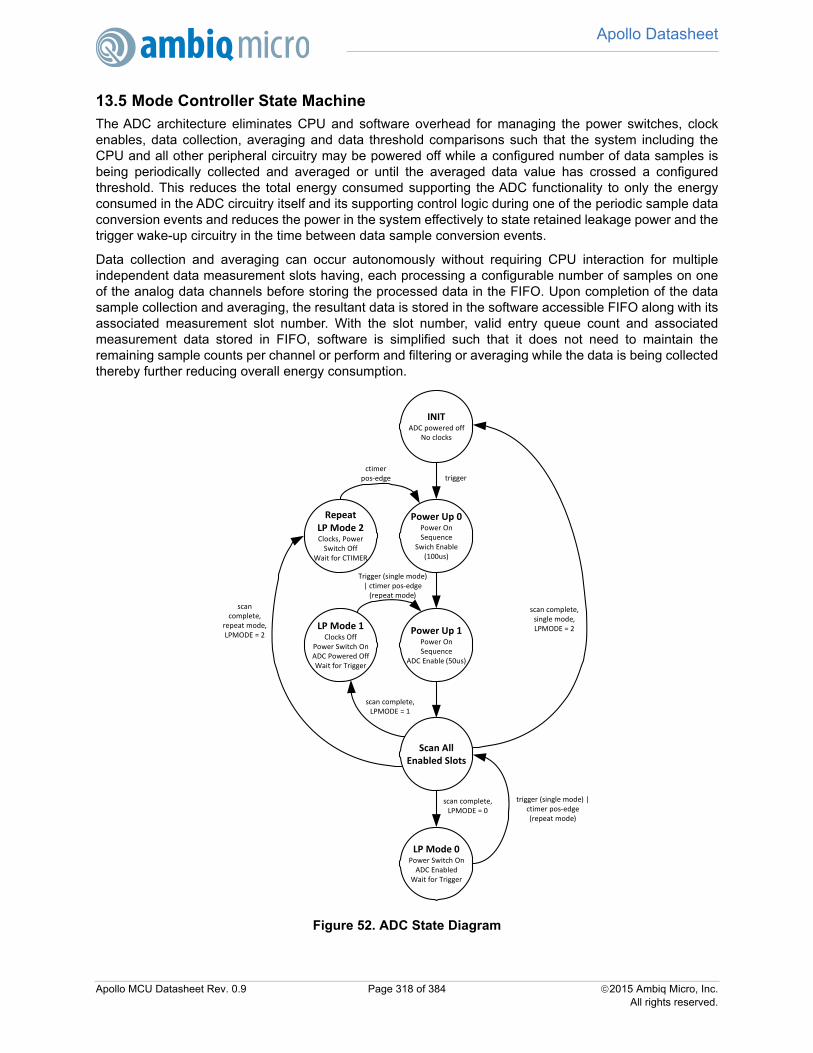
Apollo Datasheet
343
13.5 Mode Controller State MachineThe ADC architecture eliminates CPU and software overhead for managing the power switches, clockenables, data collection, averaging and data threshold comparisons such that the system including theCPU and all other peripheral circuitry may be powered off while a configured number of data samples isbeing periodically collected and averaged or until the averaged data value has crossed a configuredthreshold. This reduces the total energy consumed supporting the ADC functionality to only the energyconsumed in the ADC circuitry itself and its supporting control logic during one of the periodic sample dataconversion events and reduces the power in the system effectively to state retained leakage power and thetrigger wake-up circuitry in the time between data sample conversion events.Data collection and averaging can occur autonomously without requiring CPU interaction for multipleindependent data measurement slots having, each processing a configurable number of samples on oneof the analog data channels before storing the processed data in the FIFO. Upon completion of the datasample collection and averaging, the resultant data is stored in the software accessible FIFO along with itsassociated measurement slot number. With the slot number, valid entry queue count and associatedmeasurement data stored in FIFO, software is simplified such that it does not need to maintain theremaining sample counts per channel or perform and filtering or averaging while the data is being collectedthereby further reducing overall energy consumption.
Figure 52. ADC State Diagram
INITADC powered off
No clocks
Power Up 0Power On Sequence
Swich Enable (100us)
Scan All Enabled Slots
LP Mode 1Clocks Off
Power Switch OnADC Powered OffWait for Trigger
Power Up 1Power On Sequence
ADC Enable (50us)
RepeatLP Mode 2Clocks, Power Switch Off
Wait for CTIMER
LP Mode 0Power Switch OnADC Enabled
Wait for Trigger
triggerctimer
pos‐edge
Trigger (single mode) | ctimer pos‐edge (repeat mode)
scan complete, LPMODE = 0
scan complete, single mode, LPMODE = 2
scan complete, LPMODE = 1
scan complete,
repeat mode, LPMODE = 2
trigger (single mode) | ctimer pos‐edge (repeat mode)
Apollo MCU Datasheet Rev. 0.9 Page 318 of 384 2015 Ambiq Micro, Inc.All rights reserved.

Apollo Datasheet
343
13.6 Voltage Divider and Switchable Battery LoadThe Apollo MCU’s ADC includes a switchable voltage divider that enables the ADC to measure the inputvoltage to the VDD rail. In most systems this will be the battery voltage applied to the MCU chip. Thevoltage divider is only switched on when one of the active slots is selecting analog mux channel 12 or 13.That is only when the mode controller is ultimately triggered and powers up the ADC block for a conversionscan of all active slots. Otherwise, the voltage divider is turned off.The switchable load resistor is enabled by the BATTLOAD bit in the CFG register for the ADC. This featureis used to help estimate the health of the battery chemistry by estimating the internal resistance of thebattery.
SAR
ADC
ADC_I0 ...
ADC_I7
VDD
VSS
...
Temp Sensor VIN
Select 12,13
Input Voltage
BATTLOAD
Ron≈ 500Ω
≈ 1/3
10
KΩ
5
KΩ
Apollo MCU Datasheet Rev. 0.9 Page 319 of 384 2015 Ambiq Micro, Inc.All rights reserved.

Apollo Datasheet
343
13.7 ADC RegistersAnalog Digital Converter ControlINSTANCE 0 BASE ADDRESS:0x50008000
This is the detailed description of the Analog Digital Converter Register Block. The ADC Register Blockcontains the software control for enablement, slot configuration, clock configuration, trigger configuration,temperature sensor enablement, power modes, accumulate/divide, window comparison and interruptcontrol for the ADC functional unit.
13.7.1 Register Memory Map
Table 495: ADC Register Map
Address(s) Register Name Description
0x50008000 CFG Configuration Register
0x50008004 STAT ADC Power Status
0x50008008 SWT Software trigger
0x5000800C SL0CFG Slot 0 Configuration Register
0x50008010 SL1CFG Slot 1 Configuration Register
0x50008014 SL2CFG Slot 2 Configuration Register
0x50008018 SL3CFG Slot 3 Configuration Register
0x5000801C SL4CFG Slot 4 Configuration Register
0x50008020 SL5CFG Slot 5 Configuration Register
0x50008024 SL6CFG Slot 6 Configuration Register
0x50008028 SL7CFG Slot 7 Configuration Register
0x5000802C WLIM Window Comparator Limits Register
0x50008030 FIFO FIFO Data and Valid Count Register
0x50008200 INTEN ADC Interrupt registers: Enable
0x50008204 INTSTAT ADC Interrupt registers: Status
0x50008208 INTCLR ADC Interrupt registers: Clear
0x5000820C INTSET ADC Interrupt registers: Set
Apollo MCU Datasheet Rev. 0.9 Page 320 of 384 2015 Ambiq Micro, Inc.All rights reserved.

Apollo Datasheet
343
13.7.2 ADC Registers13.7.2.1 CFG Register
Configuration Register
OFFSET: 0x00000000
INSTANCE 0 ADDRESS: 0x50008000
The ADC Configuration Register contains the software control for selecting the clock frequency used forthe SAR conversions, the trigger polarity, the trigger select, the reference voltage select, the operatingmode (current control for high frequency conversions), the low power mode, the operating mode (singlescan per trigger vs. repeating mode), temperature sensor enable and ADC enable.
Table 496: CFG Register
31
30
29
28
27
26
25
24
23
22
21
20
19
18
17
16
15
14
13
12
11
10
09
08
07
06
05
04
03
02
01
00
RSVD
CLK
SE
L
RSVD
TR
IGP
OL
TRIGSEL RSVD
RE
FS
EL
OP
MO
DE
LPM
OD
E
RP
TE
N
TM
PS
PW
R
AD
CE
N
Table 497: CFG Register Bits
Bit Name Reset RW Description
31:27 RSVD 0x0 RORESERVED.
26:24 CLKSEL 0x0 RW
Select the source and frequency for the ADC clock. All values not enumer-ated below are undefined.
OFF = 0x0 - Low Power Mode.12MHZ = 0x1 - 12 MHz ADC clock.6MHZ = 0x2 - 6 MHz ADC clock.3MHZ = 0x3 - 3 MHz ADC clock.1_5MHZ = 0x4 - 1.5 MHz ADC clock.
23:21 RSVD 0x0 RORESERVED.
20 TRIGPOL 0x0 RW
This bit selects the ADC trigger polarity for external off chip triggers.
RISING_EDGE = 0x0 - Trigger on rising edge.FALLING_EDGE = 0x1 - Trigger on falling edge.
19:16 TRIGSEL 0x0 RW
Select the ADC trigger source.
EXT0 = 0x0 - Off chip External Trigger0 (ADC_ET0)EXT1 = 0x1 - Off chip External Trigger1 (ADC_ET1)EXT2 = 0x2 - Off chip External Trigger2 (ADC_ET2)EXT3 = 0x3 - Off chip External Trigger3 (ADC_ET3)EXT4 = 0x4 - Off chip External Trigger4 (ADC_ET4)EXT5 = 0x5 - Off chip External Trigger5 (ADC_ET5)EXT6 = 0x6 - Off chip External Trigger6 (ADC_ET6)EXT7 = 0x7 - Off chip External Trigger7 (ADC_ET7)SWT = 0x8 - Software Trigger
Apollo MCU Datasheet Rev. 0.9 Page 321 of 384 2015 Ambiq Micro, Inc.All rights reserved.

Apollo Datasheet
343
15:10 RSVD 0x0 RORESERVED.
9:8 REFSEL 0x0 RW
Select the ADC reference voltage.
INTERNAL = 0x0 - Internal Bandgap Reference VoltageVDD = 0x1 - Select VDD as the ADEC reference voltage.ADCREF = 0x2 - Off Chip Reference (ADC_REF)
7:5 OPMODE 0x0 RW
Select the sample rate mode. It adjusts the current in the ADC for highersample rates. A 12 MHz ADC clock can result in a sample rate up to800 kSps depending on the trigger or repeating mode rate. A 1.5 MHz ADCclock can result in a sample rate up to 125 kSps. NOTE: All other values not specified below are undefined.
SAMPLE_RATE_LE_125KSPS = 0x0 - Sample Rate < 125 kSpsSAMPLE_RATE_125K_800KSPS = 0x2 - Sample Rate 125 kSps to800 kSps. NOTE: When running on a 12 MHz ADC clock, OPMODE settings otherthan 0x0 are only valid when Vdd is > 2.0 V.
4:3 LPMODE 0x0 RW
Select power mode to enter between active scans.
MODE0 = 0x0 - Low Power Mode 0 (2'b00). Leaves the ADC fully poweredbetween scans with no latency between a trigger event and sample datacollection.MODE1 = 0x1 - Low Power Mode 1 (2'b01). Enables a low power mode forthe ADC between scans requiring 50us initialization time (latency) betweena trigger event and the scan (assuming the HFRC remains running and theMCU is not in deepsleep mode in which case additional startup latency forHFRC startup is required).MODE2 = 0x2 - Low Power Mode 2 (2'b10). Disconnects power and clocksto the ADC effectively eliminating all active power associated with the ADCbetween scans. This mode requires 150us initialization (again, assumingthe HFRC remains running and the MCU is not in deepsleep mode in whichcase additional startup latency for HFRC startup is required).MODE_UNDEFINED = 0x3 - Undefined Mode (2'b11)
2 RPTEN 0x0RWX
This bit enables Repeating Scan Mode.
SINGLE_SCAN = 0x0 - In Single Scan Mode, the ADC will complete a sin-gle scan upon each trigger event.REPEATING_SCAN = 0x1 - In Repeating Scan Mode, the ADC will com-plete it's first scan upon the initial trigger event and all subsequent scans willoccur at regular intervals defined by the configuration programmed for theCTTMRA3 internal timer until the timer is disabled or the ADC is disabled.
1 TMPSPWR 0x0 RW
This enables power to the temperature sensor module. After setting this bit,the temperature sensor will remain powered down while the ADC is power isdisconnected (i.e, when the ADC PWDSTAT is 2'b10).
DIS = 0x0 - Power down the temperature sensor.EN = 0x1 - Enable the temperature sensor when the ADC is in it's activestate.
0 ADCEN 0x0 RW
This bit enables the ADC module. While the ADC is enabled, the ADCCFGand SLOT Configuration regsiter settings must remain stable andunchanged.
DIS = 0x0 - Disable the ADC module.EN = 0x1 - Enable the ADC module.
Table 497: CFG Register Bits
Bit Name Reset RW Description
Apollo MCU Datasheet Rev. 0.9 Page 322 of 384 2015 Ambiq Micro, Inc.All rights reserved.

Apollo Datasheet
343
13.7.2.2 STAT RegisterADC Power Status
OFFSET: 0x00000004
INSTANCE 0 ADDRESS: 0x50008004
This register indicates the power status for the ADC. ADC power mode 0 indicates the ADC is in it's fullpower state and is ready to process scans. ADC Power mode 1 indicated the ADC power switch is on, butthe ADC SAR module is in a low power state. From this state, a trigger will bring the ADC into it's activestate after a 50us calibration period. ADC power mode 2 indicates the ADC is in it's lowest power state.
13.7.2.3 SWT Register
Software trigger
OFFSET: 0x00000008
INSTANCE 0 ADDRESS: 0x50008008
This register enables initiating an ADC scan through software.
Table 498: STAT Register
31
30
29
28
27
26
25
24
23
22
21
20
19
18
17
16
15
14
13
12
11
10
09
08
07
06
05
04
03
02
01
00
RSVD
PW
DS
TAT
Table 499: STAT Register Bits
Bit Name Reset RW Description
31:2 RSVD 0x0 RORESERVED.
1:0 PWDSTAT 0x0 RO
Indicates the power-status of the ADC.
ON = 0x0 - Powered on.SWITCH_ON_SAR_OFF = 0x1 - Power switch on, ADC Low Power Mode1.POWER_SWITCH_OFF = 0x2 - Power switch off, ADC disabled.
Table 500: SWT Register
31
30
29
28
27
26
25
24
23
22
21
20
19
18
17
16
15
14
13
12
11
10
09
08
07
06
05
04
03
02
01
00
RSVD SWT
Apollo MCU Datasheet Rev. 0.9 Page 323 of 384 2015 Ambiq Micro, Inc.All rights reserved.

Apollo Datasheet
343
13.7.2.4 SL0CFG Register
Slot 0 Configuration Register
OFFSET: 0x0000000C
INSTANCE 0 ADDRESS: 0x5000800C
Slot 0 Configuration Register
Table 501: SWT Register Bits
Bit Name Reset RW Description
31:8 RSVD 0x0 RORESERVED.
7:0 SWT 0x0 RW
Writing 0x37 to this register generates a software trigger.
GEN_SW_TRIGGER = 0x37 - Writing this value generates a software trig-ger.
Table 502: SL0CFG Register
31
30
29
28
27
26
25
24
23
22
21
20
19
18
17
16
15
14
13
12
11
10
09
08
07
06
05
04
03
02
01
00
RSVD
AD
SE
L0
RSVD
TH
SE
L0
RSVD CHSEL0 RSVD
WC
EN
0
SLE
N0
Table 503: SL0CFG Register Bits
Bit Name Reset RW Description
31:27 RSVD 0x0 RORESERVED.
26:24 ADSEL0 0x0 RW
Select the number of measurements to average in the accumulate dividemodule for this slot.
AVG_1_MSRMT = 0x0 - Average in 1 measurement in the accumulatedivide module for this slot.AVG_2_MSRMTS = 0x1 - Average in 2 measurements in the accumulatedivide module for this slot.AVG_4_MSRMTS = 0x2 - Average in 4 measurements in the accumulatedivide module for this slot.AVG_8_MSRMT = 0x3 - Average in 8 measurements in the accumulatedivide module for this slot.AVG_16_MSRMTS = 0x4 - Average in 16 measurements in the accumulatedivide module for this slot.AVG_32_MSRMTS = 0x5 - Average in 32 measurements in the accumulatedivide module for this slot.AVG_64_MSRMTS = 0x6 - Average in 64 measurements in the accumulatedivide module for this slot.AVG_128_MSRMTS = 0x7 - Average in 128 measurements in the accumu-late divide module for this slot.
Apollo MCU Datasheet Rev. 0.9 Page 324 of 384 2015 Ambiq Micro, Inc.All rights reserved.

Apollo Datasheet
343
23:19 RSVD 0x0 RORESERVED.
18:16 THSEL0 0x0 RW
Select the track and hold delay for this slot. NOTE: The track and holddelay must be less than 50us for correct operation. When the ADC is con-figured to use the 1.5Mhz clock, the track and hold delay cannot exceed 64clocks.
1_ADC_CLK = 0x0 - 1 ADC clock cycle.2_ADC_CLKS = 0x1 - 2 ADC clock cycles.4_ADC_CLKS = 0x2 - 4 ADC clock cycles.8_ADC_CLKS = 0x3 - 8 ADC clock cycles.16_ADC_CLKS = 0x4 - 16 ADC clock cycles.32_ADC_CLKS = 0x5 - 32 ADC clock cycles.64_ADC_CLKS = 0x6 - 64 ADC clock cycles.128_ADC_CLKS = 0x7 - 128 ADC clock cycles.
15:12 RSVD 0x0 RORESERVED.
11:8 CHSEL0 0x0 RW
Select one of the 13 channel inputs for this slot.
EXT0 = 0x0 - ADC_EXT0 external GPIO pin connection.EXT1 = 0x1 - ADC_EXT1 external GPIO pin connection.EXT2 = 0x2 - ADC_EXT2 external GPIO pin connection.EXT3 = 0x3 - ADC_EXT3 external GPIO pin connection.EXT4 = 0x4 - ADC_EXT4 external GPIO pin connection.EXT5 = 0x5 - ADC_EXT5 external GPIO pin connection.EXT6 = 0x6 - ADC_EXT6 external GPIO pin connection.EXT7 = 0x7 - ADC_EXT7 external GPIO pin connection.TEMP = 0x8 - ADC_TEMP internal temperature sensor.VDD = 0x9 - ADC_VDD internal power rail connection.VSS = 0xA - ADC_VSS internal ground connection.VBATT = 0xC - ADC_VBATT internal voltage divide-by-3 connection to inputpower rail.
7:2 RSVD 0x0 RORESERVED.
1 WCEN0 0x0 RWThis bit enables the window compare function for slot 0.
WCEN = 0x1 - Enable the window compare for slot 0.
0 SLEN0 0x0 RWThis bit enables slot 0 for ADC conversions.
SLEN = 0x1 - Enable slot 0 for ADC conversions.
Table 503: SL0CFG Register Bits
Bit Name Reset RW Description
Apollo MCU Datasheet Rev. 0.9 Page 325 of 384 2015 Ambiq Micro, Inc.All rights reserved.

Apollo Datasheet
343
13.7.2.5 SL1CFG RegisterSlot 1 Configuration Register
OFFSET: 0x00000010
INSTANCE 0 ADDRESS: 0x50008010
Slot 1 Configuration Register
Table 504: SL1CFG Register
31
30
29
28
27
26
25
24
23
22
21
20
19
18
17
16
15
14
13
12
11
10
09
08
07
06
05
04
03
02
01
00
RSVD
AD
SE
L1
RSVD
TH
SE
L1
RSVD CHSEL1 RSVD
WC
EN
1
SLE
N1
Table 505: SL1CFG Register Bits
Bit Name Reset RW Description
31:27 RSVD 0x0 RORESERVED.
26:24 ADSEL1 0x0 RW
Select the number of measurements to average in the accumulate dividemodule for this slot.
AVG_1_MSRMT = 0x0 - Average in 1 measurement in the accumulatedivide module for this slot.AVG_2_MSRMTS = 0x1 - Average in 2 measurements in the accumulatedivide module for this slot.AVG_4_MSRMTS = 0x2 - Average in 4 measurements in the accumulatedivide module for this slot.AVG_8_MSRMT = 0x3 - Average in 8 measurements in the accumulatedivide module for this slot.AVG_16_MSRMTS = 0x4 - Average in 16 measurements in the accumulatedivide module for this slot.AVG_32_MSRMTS = 0x5 - Average in 32 measurements in the accumulatedivide module for this slot.AVG_64_MSRMTS = 0x6 - Average in 64 measurements in the accumulatedivide module for this slot.AVG_128_MSRMTS = 0x7 - Average in 128 measurements in the accumu-late divide module for this slot.
23:19 RSVD 0x0 RORESERVED.
Apollo MCU Datasheet Rev. 0.9 Page 326 of 384 2015 Ambiq Micro, Inc.All rights reserved.

Apollo Datasheet
343
18:16 THSEL1 0x0 RW
Select the track and hold delay for this slot. NOTE: The track and holddelay must be less than 50us for correct operation. When the ADC is con-figured to use the 1.5 Mhz clock, the track and hold delay cannot exceed 64clocks.
1_ADC_CLK = 0x0 - 1 ADC clock cycle.2_ADC_CLKS = 0x1 - 2 ADC clock cycles.4_ADC_CLKS = 0x2 - 4 ADC clock cycles.8_ADC_CLKS = 0x3 - 8 ADC clock cycles.16_ADC_CLKS = 0x4 - 16 ADC clock cycles.32_ADC_CLKS = 0x5 - 32 ADC clock cycles.64_ADC_CLKS = 0x6 - 64 ADC clock cycles.128_ADC_CLKS = 0x7 - 128 ADC clock cycles.
15:12 RSVD 0x0 RORESERVED.
11:8 CHSEL1 0x0 RW
Select one of the 13 channel inputs for this slot.
EXT0 = 0x0 - ADC_EXT0 external GPIO pin connection.EXT1 = 0x1 - ADC_EXT1 external GPIO pin connection.EXT2 = 0x2 - ADC_EXT2 external GPIO pin connection.EXT3 = 0x3 - ADC_EXT3 external GPIO pin connection.EXT4 = 0x4 - ADC_EXT4 external GPIO pin connection.EXT5 = 0x5 - ADC_EXT5 external GPIO pin connection.EXT6 = 0x6 - ADC_EXT6 external GPIO pin connection.EXT7 = 0x7 - ADC_EXT7 external GPIO pin connection.TEMP = 0x8 - ADC_TEMP internal temperature sensor.VDD = 0x9 - ADC_VDD internal power rail connection.VSS = 0xA - ADC_VSS internal ground connection.VBATT = 0xC - ADC_VBATT internal voltage divide-by-3 connection to inputpower rail.
7:2 RSVD 0x0 RORESERVED.
1 WCEN1 0x0 RWThis bit enables the window compare function for slot 1.
WCEN = 0x1 - Enable the window compare for slot 1.
0 SLEN1 0x0 RWThis bit enables slot 1 for ADC conversions.
SLEN = 0x1 - Enable slot 1 for ADC conversions.
Table 505: SL1CFG Register Bits
Bit Name Reset RW Description
Apollo MCU Datasheet Rev. 0.9 Page 327 of 384 2015 Ambiq Micro, Inc.All rights reserved.

Apollo Datasheet
343
13.7.2.6 SL2CFG RegisterSlot 2 Configuration Register
OFFSET: 0x00000014
INSTANCE 0 ADDRESS: 0x50008014
Slot 2 Configuration Register
Table 506: SL2CFG Register
31
30
29
28
27
26
25
24
23
22
21
20
19
18
17
16
15
14
13
12
11
10
09
08
07
06
05
04
03
02
01
00
RSVD
AD
SE
L2
RSVD
TH
SE
L2
RSVD CHSEL2 RSVD
WC
EN
2
SLE
N2
Table 507: SL2CFG Register Bits
Bit Name Reset RW Description
31:27 RSVD 0x0 RORESERVED.
26:24 ADSEL2 0x0 RW
Select the number of measurements to average in the accumulate dividemodule for this slot.
AVG_1_MSRMT = 0x0 - Average in 1 measurement in the accumulatedivide module for this slot.AVG_2_MSRMTS = 0x1 - Average in 2 measurements in the accumulatedivide module for this slot.AVG_4_MSRMTS = 0x2 - Average in 4 measurements in the accumulatedivide module for this slot.AVG_8_MSRMT = 0x3 - Average in 8 measurements in the accumulatedivide module for this slot.AVG_16_MSRMTS = 0x4 - Average in 16 measurements in the accumulatedivide module for this slot.AVG_32_MSRMTS = 0x5 - Average in 32 measurements in the accumulatedivide module for this slot.AVG_64_MSRMTS = 0x6 - Average in 64 measurements in the accumulatedivide module for this slot.AVG_128_MSRMTS = 0x7 - Average in 128 measurements in the accumu-late divide module for this slot.
23:19 RSVD 0x0 RORESERVED.
Apollo MCU Datasheet Rev. 0.9 Page 328 of 384 2015 Ambiq Micro, Inc.All rights reserved.

Apollo Datasheet
343
18:16 THSEL2 0x0 RW
Select the track and hold delay for this slot. NOTE: The track and holddelay must be less than 50us for correct operation. When the ADC is con-figured to use the 1.5Mhz clock, the track and hold delay cannot exceed 64clocks.
1_ADC_CLK = 0x0 - 1 ADC clock cycle.2_ADC_CLKS = 0x1 - 2 ADC clock cycles.4_ADC_CLKS = 0x2 - 4 ADC clock cycles.8_ADC_CLKS = 0x3 - 8 ADC clock cycles.16_ADC_CLKS = 0x4 - 16 ADC clock cycles.32_ADC_CLKS = 0x5 - 32 ADC clock cycles.64_ADC_CLKS = 0x6 - 64 ADC clock cycles.128_ADC_CLKS = 0x7 - 128 ADC clock cycles.
15:12 RSVD 0x0 RORESERVED.
11:8 CHSEL2 0x0 RW
Select one of the 13 channel inputs for this slot.
EXT0 = 0x0 - ADC_EXT0 external GPIO pin connection.EXT1 = 0x1 - ADC_EXT1 external GPIO pin connection.EXT2 = 0x2 - ADC_EXT2 external GPIO pin connection.EXT3 = 0x3 - ADC_EXT3 external GPIO pin connection.EXT4 = 0x4 - ADC_EXT4 external GPIO pin connection.EXT5 = 0x5 - ADC_EXT5 external GPIO pin connection.EXT6 = 0x6 - ADC_EXT6 external GPIO pin connection.EXT7 = 0x7 - ADC_EXT7 external GPIO pin connection.TEMP = 0x8 - ADC_TEMP internal temperature sensor.VDD = 0x9 - ADC_VDD internal power rail connection.VSS = 0xA - ADC_VSS internal ground connection.VBATT = 0xC - ADC_VBATT internal voltage divide-by-3 connection to inputpower rail.
7:2 RSVD 0x0 RORESERVED.
1 WCEN2 0x0 RWThis bit enables the window compare function for slot 2.
WCEN = 0x1 - Enable the window compare for slot 2.
0 SLEN2 0x0 RWThis bit enables slot 2 for ADC conversions.
SLEN = 0x1 - Enable slot 2 for ADC conversions.
Table 507: SL2CFG Register Bits
Bit Name Reset RW Description
Apollo MCU Datasheet Rev. 0.9 Page 329 of 384 2015 Ambiq Micro, Inc.All rights reserved.

Apollo Datasheet
343
13.7.2.7 SL3CFG RegisterSlot 3 Configuration Register
OFFSET: 0x00000018
INSTANCE 0 ADDRESS: 0x50008018
Slot 3 Configuration Register
Table 508: SL3CFG Register
31
30
29
28
27
26
25
24
23
22
21
20
19
18
17
16
15
14
13
12
11
10
09
08
07
06
05
04
03
02
01
00
RSVD
AD
SE
L3
RSVD
TH
SE
L3
RSVD CHSEL3 RSVD
WC
EN
3
SLE
N3
Table 509: SL3CFG Register Bits
Bit Name Reset RW Description
31:27 RSVD 0x0 RORESERVED.
26:24 ADSEL3 0x0 RW
Select the number of measurements to average in the accumulate dividemodule for this slot.
AVG_1_MSRMT = 0x0 - Average in 1 measurement in the accumulatedivide module for this slot.AVG_2_MSRMTS = 0x1 - Average in 2 measurements in the accumulatedivide module for this slot.AVG_4_MSRMTS = 0x2 - Average in 4 measurements in the accumulatedivide module for this slot.AVG_8_MSRMT = 0x3 - Average in 8 measurements in the accumulatedivide module for this slot.AVG_16_MSRMTS = 0x4 - Average in 16 measurements in the accumulatedivide module for this slot.AVG_32_MSRMTS = 0x5 - Average in 32 measurements in the accumulatedivide module for this slot.AVG_64_MSRMTS = 0x6 - Average in 64 measurements in the accumulatedivide module for this slot.AVG_128_MSRMTS = 0x7 - Average in 128 measurements in the accumu-late divide module for this slot.
23:19 RSVD 0x0 RORESERVED.
Apollo MCU Datasheet Rev. 0.9 Page 330 of 384 2015 Ambiq Micro, Inc.All rights reserved.

Apollo Datasheet
343
18:16 THSEL3 0x0 RW
Select the track and hold delay for this slot. NOTE: The track and holddelay must be less than 50us for correct operation. When the ADC is con-figured to use the 1.5Mhz clock, the track and hold delay cannot exceed 64clocks.
1_ADC_CLK = 0x0 - 1 ADC clock cycle.2_ADC_CLKS = 0x1 - 2 ADC clock cycles.4_ADC_CLKS = 0x2 - 4 ADC clock cycles.8_ADC_CLKS = 0x3 - 8 ADC clock cycles.16_ADC_CLKS = 0x4 - 16 ADC clock cycles.32_ADC_CLKS = 0x5 - 32 ADC clock cycles.64_ADC_CLKS = 0x6 - 64 ADC clock cycles.128_ADC_CLKS = 0x7 - 128 ADC clock cycles.
15:12 RSVD 0x0 RORESERVED.
11:8 CHSEL3 0x0 RW
Select one of the 13 channel inputs for this slot.
EXT0 = 0x0 - ADC_EXT0 external GPIO pin connection.EXT1 = 0x1 - ADC_EXT1 external GPIO pin connection.EXT2 = 0x2 - ADC_EXT2 external GPIO pin connection.EXT3 = 0x3 - ADC_EXT3 external GPIO pin connection.EXT4 = 0x4 - ADC_EXT4 external GPIO pin connection.EXT5 = 0x5 - ADC_EXT5 external GPIO pin connection.EXT6 = 0x6 - ADC_EXT6 external GPIO pin connection.EXT7 = 0x7 - ADC_EXT7 external GPIO pin connection.TEMP = 0x8 - ADC_TEMP internal temperature sensor.VDD = 0x9 - ADC_VDD internal power rail connection.VSS = 0xA - ADC_VSS internal ground connection.VBATT = 0xC - ADC_VBATT internal voltage divide-by-3 connection to inputpower rail.
7:2 RSVD 0x0 RORESERVED.
1 WCEN3 0x0 RWThis bit enables the window compare function for slot 3.
WCEN = 0x1 - Enable the window compare for slot 3.
0 SLEN3 0x0 RWThis bit enables slot 3 for ADC conversions.
SLEN = 0x1 - Enable slot 3 for ADC conversions.
Table 509: SL3CFG Register Bits
Bit Name Reset RW Description
Apollo MCU Datasheet Rev. 0.9 Page 331 of 384 2015 Ambiq Micro, Inc.All rights reserved.

Apollo Datasheet
343
13.7.2.8 SL4CFG RegisterSlot 4 Configuration Register
OFFSET: 0x0000001C
INSTANCE 0 ADDRESS: 0x5000801C
Slot 4 Configuration Register
Table 510: SL4CFG Register
31
30
29
28
27
26
25
24
23
22
21
20
19
18
17
16
15
14
13
12
11
10
09
08
07
06
05
04
03
02
01
00
RSVD
AD
SE
L4
RSVD
TH
SE
L4
RSVD CHSEL4 RSVD
WC
EN
4
SLE
N4
Table 511: SL4CFG Register Bits
Bit Name Reset RW Description
31:27 RSVD 0x0 RORESERVED.
26:24 ADSEL4 0x0 RW
Select the number of measurements to average in the accumulate dividemodule for this slot.
AVG_1_MSRMT = 0x0 - Average in 1 measurement in the accumulatedivide module for this slot.AVG_2_MSRMTS = 0x1 - Average in 2 measurements in the accumulatedivide module for this slot.AVG_4_MSRMTS = 0x2 - Average in 4 measurements in the accumulatedivide module for this slot.AVG_8_MSRMT = 0x3 - Average in 8 measurements in the accumulatedivide module for this slot.AVG_16_MSRMTS = 0x4 - Average in 16 measurements in the accumulatedivide module for this slot.AVG_32_MSRMTS = 0x5 - Average in 32 measurements in the accumulatedivide module for this slot.AVG_64_MSRMTS = 0x6 - Average in 64 measurements in the accumulatedivide module for this slot.AVG_128_MSRMTS = 0x7 - Average in 128 measurements in the accumu-late divide module for this slot.
23:19 RSVD 0x0 RORESERVED.
Apollo MCU Datasheet Rev. 0.9 Page 332 of 384 2015 Ambiq Micro, Inc.All rights reserved.

Apollo Datasheet
343
18:16 THSEL4 0x0 RW
Select the track and hold delay for this slot. NOTE: The track and holddelay must be less than 50us for correct operation. When the ADC is con-figured to use the 1.5Mhz clock, the track and hold delay cannot exceed 64clocks.
1_ADC_CLK = 0x0 - 1 ADC clock cycle.2_ADC_CLKS = 0x1 - 2 ADC clock cycles.4_ADC_CLKS = 0x2 - 4 ADC clock cycles.8_ADC_CLKS = 0x3 - 8 ADC clock cycles.16_ADC_CLKS = 0x4 - 16 ADC clock cycles.32_ADC_CLKS = 0x5 - 32 ADC clock cycles.64_ADC_CLKS = 0x6 - 64 ADC clock cycles.128_ADC_CLKS = 0x7 - 128 ADC clock cycles.
15:12 RSVD 0x0 RORESERVED.
11:8 CHSEL4 0x0 RW
Select one of the 13 channel inputs for this slot.
EXT0 = 0x0 - ADC_EXT0 external GPIO pin connection.EXT1 = 0x1 - ADC_EXT1 external GPIO pin connection.EXT2 = 0x2 - ADC_EXT2 external GPIO pin connection.EXT3 = 0x3 - ADC_EXT3 external GPIO pin connection.EXT4 = 0x4 - ADC_EXT4 external GPIO pin connection.EXT5 = 0x5 - ADC_EXT5 external GPIO pin connection.EXT6 = 0x6 - ADC_EXT6 external GPIO pin connection.EXT7 = 0x7 - ADC_EXT7 external GPIO pin connection.TEMP = 0x8 - ADC_TEMP internal temperature sensor.VDD = 0x9 - ADC_VDD internal power rail connection.VSS = 0xA - ADC_VSS internal ground connection.VBATT = 0xC - ADC_VBATT internal voltage divide-by-3 connection to inputpower rail.
7:2 RSVD 0x0 RORESERVED.
1 WCEN4 0x0 RWThis bit enables the window compare function for slot 4.
WCEN = 0x1 - Enable the window compare for slot 4.
0 SLEN4 0x0 RWThis bit enables slot 4 for ADC conversions.
SLEN = 0x1 - Enable slot 4 for ADC conversions.
Table 511: SL4CFG Register Bits
Bit Name Reset RW Description
Apollo MCU Datasheet Rev. 0.9 Page 333 of 384 2015 Ambiq Micro, Inc.All rights reserved.

Apollo Datasheet
343
13.7.2.9 SL5CFG RegisterSlot 5 Configuration Register
OFFSET: 0x00000020
INSTANCE 0 ADDRESS: 0x50008020
Slot 5 Configuration Register
Table 512: SL5CFG Register
31
30
29
28
27
26
25
24
23
22
21
20
19
18
17
16
15
14
13
12
11
10
09
08
07
06
05
04
03
02
01
00
RSVD
AD
SE
L5
RSVD
TH
SE
L5
RSVD CHSEL5 RSVD
WC
EN
5
SLE
N5
Table 513: SL5CFG Register Bits
Bit Name Reset RW Description
31:27 RSVD 0x0 RORESERVED.
26:24 ADSEL5 0x0 RW
Select number of measurements to average in the accumulate divide mod-ule for this slot.
AVG_1_MSRMT = 0x0 - Average in 1 measurement in the accumulatedivide module for this slot.AVG_2_MSRMTS = 0x1 - Average in 2 measurements in the accumulatedivide module for this slot.AVG_4_MSRMTS = 0x2 - Average in 4 measurements in the accumulatedivide module for this slot.AVG_8_MSRMT = 0x3 - Average in 8 measurements in the accumulatedivide module for this slot.AVG_16_MSRMTS = 0x4 - Average in 16 measurements in the accumulatedivide module for this slot.AVG_32_MSRMTS = 0x5 - Average in 32 measurements in the accumulatedivide module for this slot.AVG_64_MSRMTS = 0x6 - Average in 64 measurements in the accumulatedivide module for this slot.AVG_128_MSRMTS = 0x7 - Average in 128 measurements in the accumu-late divide module for this slot.
23:19 RSVD 0x0 RORESERVED.
18:16 THSEL5 0x0 RW
Select track and hold delay for this slot. NOTE: The track and hold delaymust be less than 50us for correct operation. When the ADC is configuredto use the 1.5Mhz clock, the track and hold delay cannot exceed 64 clocks.
1_ADC_CLK = 0x0 - 1 ADC clock cycle.2_ADC_CLKS = 0x1 - 2 ADC clock cycles.4_ADC_CLKS = 0x2 - 4 ADC clock cycles.8_ADC_CLKS = 0x3 - 8 ADC clock cycles.16_ADC_CLKS = 0x4 - 16 ADC clock cycles.32_ADC_CLKS = 0x5 - 32 ADC clock cycles.64_ADC_CLKS = 0x6 - 64 ADC clock cycles.128_ADC_CLKS = 0x7 - 128 ADC clock cycles.
Apollo MCU Datasheet Rev. 0.9 Page 334 of 384 2015 Ambiq Micro, Inc.All rights reserved.

Apollo Datasheet
343
15:12 RSVD 0x0 RORESERVED.
11:8 CHSEL5 0x0 RW
Select one of the 13 channel inputs for this slot.
EXT0 = 0x0 - ADC_EXT0 external GPIO pin connection.EXT1 = 0x1 - ADC_EXT1 external GPIO pin connection.EXT2 = 0x2 - ADC_EXT2 external GPIO pin connection.EXT3 = 0x3 - ADC_EXT3 external GPIO pin connection.EXT4 = 0x4 - ADC_EXT4 external GPIO pin connection.EXT5 = 0x5 - ADC_EXT5 external GPIO pin connection.EXT6 = 0x6 - ADC_EXT6 external GPIO pin connection.EXT7 = 0x7 - ADC_EXT7 external GPIO pin connection.TEMP = 0x8 - ADC_TEMP internal temperature sensor.VDD = 0x9 - ADC_VDD internal power rail connection.VSS = 0xA - ADC_VSS internal ground connection.VBATT = 0xC - ADC_VBATT internal voltage divide-by-3 connection to inputpower rail.
7:2 RSVD 0x0 RORESERVED.
1 WCEN5 0x0 RWThis bit enables the window compare function for slot 5.
WCEN = 0x1 - Enable the window compare for slot 5.
0 SLEN5 0x0 RWThis bit enables slot 5 for ADC conversions.
SLEN = 0x1 - Enable slot 5 for ADC conversions.
Table 513: SL5CFG Register Bits
Bit Name Reset RW Description
Apollo MCU Datasheet Rev. 0.9 Page 335 of 384 2015 Ambiq Micro, Inc.All rights reserved.

Apollo Datasheet
343
13.7.2.10 SL6CFG RegisterSlot 6 Configuration Register
OFFSET: 0x00000024
INSTANCE 0 ADDRESS: 0x50008024
Slot 6 Configuration Register
Table 514: SL6CFG Register
31
30
29
28
27
26
25
24
23
22
21
20
19
18
17
16
15
14
13
12
11
10
09
08
07
06
05
04
03
02
01
00
RSVD
AD
SE
L6
RSVD
TH
SE
L6
RSVD CHSEL6 RSVD
WC
EN
6
SLE
N6
Table 515: SL6CFG Register Bits
Bit Name Reset RW Description
31:27 RSVD 0x0 RORESERVED.
26:24 ADSEL6 0x0 RW
Select the number of measurements to average in the accumulate dividemodule for this slot.
AVG_1_MSRMT = 0x0 - Average in 1 measurement in the accumulatedivide module for this slot.AVG_2_MSRMTS = 0x1 - Average in 2 measurements in the accumulatedivide module for this slot.AVG_4_MSRMTS = 0x2 - Average in 4 measurements in the accumulatedivide module for this slot.AVG_8_MSRMT = 0x3 - Average in 8 measurements in the accumulatedivide module for this slot.AVG_16_MSRMTS = 0x4 - Average in 16 measurements in the accumulatedivide module for this slot.AVG_32_MSRMTS = 0x5 - Average in 32 measurements in the accumulatedivide module for this slot.AVG_64_MSRMTS = 0x6 - Average in 64 measurements in the accumulatedivide module for this slot.AVG_128_MSRMTS = 0x7 - Average in 128 measurements in the accumu-late divide module for this slot.
23:19 RSVD 0x0 RORESERVED.
18:16 THSEL6 0x0 RW
Select track and hold delay for this slot. NOTE: The track and hold delaymust be less than 50us for correct operation. When the ADC is configuredto use the 1.5Mhz clock, the track and hold delay cannot exceed 64 clocks.
1_ADC_CLK = 0x0 - 1 ADC clock cycle.2_ADC_CLKS = 0x1 - 2 ADC clock cycles.4_ADC_CLKS = 0x2 - 4 ADC clock cycles.8_ADC_CLKS = 0x3 - 8 ADC clock cycles.16_ADC_CLKS = 0x4 - 16 ADC clock cycles.32_ADC_CLKS = 0x5 - 32 ADC clock cycles.64_ADC_CLKS = 0x6 - 64 ADC clock cycles.128_ADC_CLKS = 0x7 - 128 ADC clock cycles.
Apollo MCU Datasheet Rev. 0.9 Page 336 of 384 2015 Ambiq Micro, Inc.All rights reserved.

Apollo Datasheet
343
13.7.2.11 SL7CFG Register
Slot 7 Configuration Register
OFFSET: 0x00000028
INSTANCE 0 ADDRESS: 0x50008028
Slot 7 Configuration Register
15:12 RSVD 0x0 RORESERVED.
11:8 CHSEL6 0x0 RW
Select one of the 13 channel inputs for this slot.
EXT0 = 0x0 - ADC_EXT0 external GPIO pin connection.EXT1 = 0x1 - ADC_EXT1 external GPIO pin connection.EXT2 = 0x2 - ADC_EXT2 external GPIO pin connection.EXT3 = 0x3 - ADC_EXT3 external GPIO pin connection.EXT4 = 0x4 - ADC_EXT4 external GPIO pin connection.EXT5 = 0x5 - ADC_EXT5 external GPIO pin connection.EXT6 = 0x6 - ADC_EXT6 external GPIO pin connection.EXT7 = 0x7 - ADC_EXT7 external GPIO pin connection.TEMP = 0x8 - ADC_TEMP internal temperature sensor.VDD = 0x9 - ADC_VDD internal power rail connection.VSS = 0xA - ADC_VSS internal ground connection.VBATT = 0xC - ADC_VBATT internal voltage divide-by-3 connection to inputpower rail.
7:2 RSVD 0x0 RORESERVED.
1 WCEN6 0x0 RWThis bit enables the window compare function for slot 6.
WCEN = 0x1 - Enable the window compare for slot 6.
0 SLEN6 0x0 RWThis bit enables slot 6 for ADC conversions.
SLEN = 0x1 - Enable slot 6 for ADC conversions.
Table 516: SL7CFG Register
31
30
29
28
27
26
25
24
23
22
21
20
19
18
17
16
15
14
13
12
11
10
09
08
07
06
05
04
03
02
01
00
RSVD
AD
SE
L7
RSVD
TH
SE
L7
RSVD CHSEL7 RSVD
WC
EN
7
SL
EN
7
Table 517: SL7CFG Register Bits
Bit Name Reset RW Description
31:27 RSVD 0x0 RORESERVED.
Table 515: SL6CFG Register Bits
Bit Name Reset RW Description
Apollo MCU Datasheet Rev. 0.9 Page 337 of 384 2015 Ambiq Micro, Inc.All rights reserved.

Apollo Datasheet
343
26:24 ADSEL7 0x0 RW
Select the number of measurements to average in the accumulate dividemodule for this slot.
AVG_1_MSRMT = 0x0 - Average in 1 measurement in the accumulatedivide module for this slot.AVG_2_MSRMTS = 0x1 - Average in 2 measurements in the accumulatedivide module for this slot.AVG_4_MSRMTS = 0x2 - Average in 4 measurements in the accumulatedivide module for this slot.AVG_8_MSRMT = 0x3 - Average in 8 measurements in the accumulatedivide module for this slot.AVG_16_MSRMTS = 0x4 - Average in 16 measurements in the accumulatedivide module for this slot.AVG_32_MSRMTS = 0x5 - Average in 32 measurements in the accumulatedivide module for this slot.AVG_64_MSRMTS = 0x6 - Average in 64 measurements in the accumulatedivide module for this slot.AVG_128_MSRMTS = 0x7 - Average in 128 measurements in the accumu-late divide module for this slot.
23:19 RSVD 0x0 RORESERVED.
18:16 THSEL7 0x0 RW
Select track and hold delay for this slot. NOTE: The track and hold delaymust be less than 50us for correct operation. When the ADC is configuredto use the 1.5Mhz clock, the track and hold delay cannot exceed 64 clocks.
1_ADC_CLK = 0x0 - 1 ADC clock cycle.2_ADC_CLKS = 0x1 - 2 ADC clock cycles.4_ADC_CLKS = 0x2 - 4 ADC clock cycles.8_ADC_CLKS = 0x3 - 8 ADC clock cycles.16_ADC_CLKS = 0x4 - 16 ADC clock cycles.32_ADC_CLKS = 0x5 - 32 ADC clock cycles.64_ADC_CLKS = 0x6 - 64 ADC clock cycles.128_ADC_CLKS = 0x7 - 128 ADC clock cycles.
15:12 RSVD 0x0 RORESERVED.
11:8 CHSEL7 0x0 RW
Select one of the 13 channel inputs for this slot.
EXT0 = 0x0 - ADC_EXT0 external GPIO pin connection.EXT1 = 0x1 - ADC_EXT1 external GPIO pin connection.EXT2 = 0x2 - ADC_EXT2 external GPIO pin connection.EXT3 = 0x3 - ADC_EXT3 external GPIO pin connection.EXT4 = 0x4 - ADC_EXT4 external GPIO pin connection.EXT5 = 0x5 - ADC_EXT5 external GPIO pin connection.EXT6 = 0x6 - ADC_EXT6 external GPIO pin connection.EXT7 = 0x7 - ADC_EXT7 external GPIO pin connection.TEMP = 0x8 - ADC_TEMP internal temperature sensor.VDD = 0x9 - ADC_VDD internal power rail connection.VSS = 0xA - ADC_VSS internal ground connection.VBATT = 0xC - ADC_VBATT internal voltage divide-by-3 connection to inputpower rail.
7:2 RSVD 0x0 RORESERVED.
1 WCEN7 0x0 RWThis bit enables the window compare function for slot 7.
WCEN = 0x1 - Enable the window compare for slot 7.
Table 517: SL7CFG Register Bits
Bit Name Reset RW Description
Apollo MCU Datasheet Rev. 0.9 Page 338 of 384 2015 Ambiq Micro, Inc.All rights reserved.

Apollo Datasheet
343
13.7.2.12 WLIM Register
Window Comparator Limits Register
OFFSET: 0x0000002C
INSTANCE 0 ADDRESS: 0x5000802C
Window Comparator Limits Register
13.7.2.13 FIFO Register
FIFO Data and Valid Count Register
OFFSET: 0x00000030
INSTANCE 0 ADDRESS: 0x50008030
The ADC FIFO Register contains the slot number and fifo data for the oldest conversion data in the FIFO.The COUNT field indicates the total number of valid entries in the FIFO. A write to this register will pop oneof the FIFO entries off the FIFO and decrease the COUNT by 1 if the COUNT is greater than zero.
0 SLEN7 0x0 RWThis bit enables slot 7 for ADC conversions.
SLEN = 0x1 - Enable slot 7 for ADC conversions.
Table 518: WLIM Register
31
30
29
28
27
26
25
24
23
22
21
20
19
18
17
16
15
14
13
12
11
10
09
08
07
06
05
04
03
02
01
00
ULIM LLIM
Table 519: WLIM Register Bits
Bit Name Reset RW Description
31:16 ULIM 0x0 RWSets the upper limit for the wondow comparator.
15:0 LLIM 0x0 RWSets the lower limit for the wondow comparator.
Table 520: FIFO Register
31
30
29
28
27
26
25
24
23
22
21
20
19
18
17
16
15
14
13
12
11
10
09
08
07
06
05
04
03
02
01
00
RSVD_27
SLO
TN
UM
RSVD_20 COUNT DATA
Table 517: SL7CFG Register Bits
Bit Name Reset RW Description
Apollo MCU Datasheet Rev. 0.9 Page 339 of 384 2015 Ambiq Micro, Inc.All rights reserved.

Apollo Datasheet
343
13.7.2.14 INTEN Register
ADC Interrupt registers: Enable
OFFSET: 0x00000200
INSTANCE 0 ADDRESS: 0x50008200
Set bits in this register to allow this module to generate the corresponding interrupt.
Table 521: FIFO Register Bits
Bit Name Reset RW Description
31:27 RSVD_27 0x0 RORESERVED.
26:24 SLOTNUM 0x0 ROSlot number associated with this FIFO data.
23:20 RSVD_20 0x0 RORESERVED.
19:16 COUNT 0x0 RONumber of valid entries in the ADC FIFO.
15:0 DATA 0x0 ROOldest data in the FIFO.
Table 522: INTEN Register
31
30
29
28
27
26
25
24
23
22
21
20
19
18
17
16
15
14
13
12
11
10
09
08
07
06
05
04
03
02
01
00
RSVDW
CIN
C
WC
EX
C
FIF
OO
VR
2
FIF
OO
VR
1
SC
NC
MP
CN
VC
MP
Table 523: INTEN Register Bits
Bit Name Reset RW Description
31:6 RSVD 0x0 RORESERVED.
5 WCINC 0x0 RWWindow comparator voltage incursion interrupt.
WCINCINT = 0x1 - Window comparitor voltage incursion interrupt.
4 WCEXC 0x0 RWWindow comparator voltage excursion interrupt.
WCEXCINT = 0x1 - Window comparitor voltage excursion interrupt.
3 FIFOOVR2 0x0 RWFIFO 100% full interrupt.
FIFOFULLINT = 0x1 - FIFO 100% full interrupt.
Apollo MCU Datasheet Rev. 0.9 Page 340 of 384 2015 Ambiq Micro, Inc.All rights reserved.

Apollo Datasheet
343
13.7.2.15 INTSTAT Register
ADC Interrupt registers: Status
OFFSET: 0x00000204
INSTANCE 0 ADDRESS: 0x50008204
Read bits from this register to discover the cause of a recent interrupt.
2 FIFOOVR1 0x0 RWFIFO 75% full interrupt.
FIFO75INT = 0x1 - FIFO 75% full interrupt.
1 SCNCMP 0x0 RWADC scan complete interrupt.
SCNCMPINT = 0x1 - ADC scan complete interrupt.
0 CNVCMP 0x0 RWADC conversion complete interrupt.
CNVCMPINT = 0x1 - ADC conversion complete interrupt.
Table 524: INTSTAT Register
31
30
29
28
27
26
25
24
23
22
21
20
19
18
17
16
15
14
13
12
11
10
09
08
07
06
05
04
03
02
01
00
RSVD
WC
INC
WC
EX
C
FIF
OO
VR
2
FIF
OO
VR
1
SC
NC
MP
CN
VC
MP
Table 525: INTSTAT Register Bits
Bit Name Reset RW Description
31:6 RSVD 0x0 RORESERVED.
5 WCINC 0x0 RWWindow comparator voltage incursion interrupt.
WCINCINT = 0x1 - Window comparitor voltage incursion interrupt.
4 WCEXC 0x0 RWWindow comparator voltage excursion interrupt.
WCEXCINT = 0x1 - Window comparitor voltage excursion interrupt.
3 FIFOOVR2 0x0 RWFIFO 100% full interrupt.
FIFOFULLINT = 0x1 - FIFO 100% full interrupt.
2 FIFOOVR1 0x0 RWFIFO 75% full interrupt.
FIFO75INT = 0x1 - FIFO 75% full interrupt.
1 SCNCMP 0x0 RWADC scan complete interrupt.
SCNCMPINT = 0x1 - ADC scan complete interrupt.
Table 523: INTEN Register Bits
Bit Name Reset RW Description
Apollo MCU Datasheet Rev. 0.9 Page 341 of 384 2015 Ambiq Micro, Inc.All rights reserved.

Apollo Datasheet
343
13.7.2.16 INTCLR Register
ADC Interrupt registers: Clear
OFFSET: 0x00000208
INSTANCE 0 ADDRESS: 0x50008208
Write a 1 to a bit in this register to clear the interrupt status associated with that bit.
0 CNVCMP 0x0 RWADC conversion complete interrupt.
CNVCMPINT = 0x1 - ADC conversion complete interrupt.
Table 526: INTCLR Register
31
30
29
28
27
26
25
24
23
22
21
20
19
18
17
16
15
14
13
12
11
10
09
08
07
06
05
04
03
02
01
00
RSVD
WC
INC
WC
EX
C
FIF
OO
VR
2
FIF
OO
VR
1
SC
NC
MP
CN
VC
MP
Table 527: INTCLR Register Bits
Bit Name Reset RW Description
31:6 RSVD 0x0 RORESERVED.
5 WCINC 0x0 RWWindow comparator voltage incursion interrupt.
WCINCINT = 0x1 - Window comparitor voltage incursion interrupt.
4 WCEXC 0x0 RWWindow comparator voltage excursion interrupt.
WCEXCINT = 0x1 - Window comparitor voltage excursion interrupt.
3 FIFOOVR2 0x0 RWFIFO 100% full interrupt.
FIFOFULLINT = 0x1 - FIFO 100% full interrupt.
2 FIFOOVR1 0x0 RWFIFO 75% full interrupt.
FIFO75INT = 0x1 - FIFO 75% full interrupt.
1 SCNCMP 0x0 RWADC scan complete interrupt.
SCNCMPINT = 0x1 - ADC scan complete interrupt.
0 CNVCMP 0x0 RWADC conversion complete interrupt.
CNVCMPINT = 0x1 - ADC conversion complete interrupt.
Table 525: INTSTAT Register Bits
Bit Name Reset RW Description
Apollo MCU Datasheet Rev. 0.9 Page 342 of 384 2015 Ambiq Micro, Inc.All rights reserved.

Apollo Datasheet
343
13.7.2.17 INTSET RegisterADC Interrupt registers: Set
OFFSET: 0x0000020C
INSTANCE 0 ADDRESS: 0x5000820C
Write a 1 to a bit in this register to instantly generate an interrupt from this module. (Generally used fortesting purposes).
Table 528: INTSET Register
31
30
29
28
27
26
25
24
23
22
21
20
19
18
17
16
15
14
13
12
11
10
09
08
07
06
05
04
03
02
01
00
RSVD
WC
INC
WC
EX
C
FIF
OO
VR
2
FIF
OO
VR
1
SC
NC
MP
CN
VC
MP
Table 529: INTSET Register Bits
Bit Name Reset RW Description
31:6 RSVD 0x0 RORESERVED.
5 WCINC 0x0 RWWindow comparator voltage incursion interrupt.
WCINCINT = 0x1 - Window comparitor voltage incursion interrupt.
4 WCEXC 0x0 RWWindow comparator voltage excursion interrupt.
WCEXCINT = 0x1 - Window comparitor voltage excursion interrupt.
3 FIFOOVR2 0x0 RWFIFO 100% full interrupt.
FIFOFULLINT = 0x1 - FIFO 100% full interrupt.
2 FIFOOVR1 0x0 RWFIFO 75% full interrupt.
FIFO75INT = 0x1 - FIFO 75% full interrupt.
1 SCNCMP 0x0 RWADC scan complete interrupt.
SCNCMPINT = 0x1 - ADC scan complete interrupt.
0 CNVCMP 0x0 RWADC conversion complete interrupt.
CNVCMPINT = 0x1 - ADC conversion complete interrupt.
Apollo MCU Datasheet Rev. 0.9 Page 343 of 384 2015 Ambiq Micro, Inc.All rights reserved.

Apollo Datasheet
350
14. Voltage Comparator Module
Figure 53. Block diagram for the Voltage Comparator Module
14.1 Functional OverviewThe Voltage Comparator Module, shown in Figure 53, measures a user-selectable voltage at all times. Itprovides interrupt and software access to the comparator output with multiple options for voltage levels it iscomparing. It can be configured to generate an interrupt when the monitored voltage rises above a user-configurable threshold or when the monitored voltage drops below a user-configurable threshold.
The voltage to be monitored is selected by programming the comparator’s positive terminal signal,PSEL[1:0] and may be any of: 1) the supply voltage (VDD), 2) the PTAT voltage from the temperaturesensor (VTEMP), or 3) two external voltage channels (CMPIN0 and CMPIN1).
The reference voltage is selected by programming the comparator’s negative terminal, NSEL[1:0] and maybe any of: 1) three external voltage channels (CMPRF0, CMPRF1, CMPRF2), or 2) the internallygenerated reference (VREFINT). The internal reference voltage is tuned using an on-chip DAC with levelselect signal LVLSEL[3:0]. When using external inputs or reference inputs, the associated pads must beconfigured using the GPIO function selects explained the GPIO document section.
The Voltage Comparator CMPOUT output will remain high while the voltage at the positive input is abovethe voltage at reference input. The CMPOUT output will transition low when the voltage at the positiveinput to the comparator falls below the reference input. The CMPOUT output is directly accessible bysoftware by reading the CMPOUT field in the status register. The OUTHI interrupt will be set if enabled andthe CMPOUT transitions high or if it is high at the time the interrupt is enabled. Similarly, the OUTLOWinterrupt will be set if enabled and the CMPOUT output transitions low or if it is low at the time the interruptis enabled.
The Voltage Comparator Module is enabled by default and may be powered off by writing 0x37 to thePWDKEY register.
VDDH
DAC
VTEMP
CMPIN0
CMPIN1
CMPRF0
CMPRF1
CMPRF2
PSEL[1:0]
+
_
LVLSEL[3:0]NSEL[1:0]
CMPOUT
POWER
DOWNPWD
Apollo MCU Datasheet Rev. 0.9 Page 344 of 384 2015 Ambiq Micro, Inc.All rights reserved.

Apollo Datasheet
350
14.2 VCOMP RegistersVoltage ComparatorINSTANCE 0 BASE ADDRESS:0x4000C000
This is the detailed description of the Voltage Comparator Register Block. The Voltage ComparatorRegister Block contains the software control for selecting the comparator inputs, powerdown control,observing comparator output status and enabling interrupts.
14.2.1 Register Memory Map
14.2.2 VCOMP Registers
14.2.2.1 CFG Register
Configuration Register
OFFSET: 0x00000000
INSTANCE 0 ADDRESS: 0x4000C000
The Voltage Comparator Configuration Register contains the software control for selecting between thefour options for the positive input as well as the multiple options for the reference input.
Table 530: VCOMP Register Map
Address(s) Register Name Description
0x4000C000 CFG Configuration Register
0x4000C004 STAT Status Register
0x4000C008 PWDKEYKey Register for Powering Down the VoltageComparator
0x4000C200 INTEN Voltage Comparator Interrupt registers: Enable
0x4000C204 INTSTAT Voltage Comparator Interrupt registers: Status
0x4000C208 INTCLR Voltage Comparator Interrupt registers: Clear
0x4000C20C INTSET Voltage Comparator Interrupt registers: Set
Table 531: CFG Register
31
30
29
28
27
26
25
24
23
22
21
20
19
18
17
16
15
14
13
12
11
10
09
08
07
06
05
04
03
02
01
00
RSVD LVLSEL RSVD
NS
EL
RSVD
PS
EL
Apollo MCU Datasheet Rev. 0.9 Page 345 of 384 2015 Ambiq Micro, Inc.All rights reserved.

Apollo Datasheet
350
Table 532: CFG Register Bits
Bit Name Reset RW Description
31:20 RSVD 0x0 ROThis bitfield is reserved for future use.
19:16 LVLSEL 0x0 RW
When the reference input NSEL is set to NSEL_DAC, this bitfield selects thevoltage level for the negative input to the comparator.
0P58V = 0x0 - Set Reference input to 0.58 Volts.0P77V = 0x1 - Set Reference input to 0.77 Volts.0P97V = 0x2 - Set Reference input to 0.97 Volts.1P16V = 0x3 - Set Reference input to 1.16 Volts.1P35V = 0x4 - Set Reference input to 1.35 Volts.1P55V = 0x5 - Set Reference input to 1.55 Volts.1P74V = 0x6 - Set Reference input to 1.74 Volts.1P93V = 0x7 - Set Reference input to 1.93 Volts.2P13V = 0x8 - Set Reference input to 2.13 Volts.2P32V = 0x9 - Set Reference input to 2.32 Volts.2P51V = 0xA - Set Reference input to 2.51 Volts.2P71V = 0xB - Set Reference input to 2.71 Volts.2P90V = 0xC - Set Reference input to 2.90 Volts.3P09V = 0xD - Set Reference input to 3.09 Volts.3P29V = 0xE - Set Reference input to 3.29 Volts.3P48V = 0xF - Set Reference input to 3.48 Volts.
15:10 RSVD 0x0 ROThis bitfield is reserved for future use.
9:8 NSEL 0x0 RW
This bitfield selects the negative input to the comparator.
CMPRF0 = 0x0 - Use comparator reference 0 for reference input.CMPRF1 = 0x1 - Use comparator reference 1 for reference input.CMPRF2 = 0x3 - Use comparator reference 2 for reference input.DAC = 0x3 - Use DAC output selected by LVLSEL for reference input.
7:2 RSVD 0x0 ROThis bitfield is reserved for future use.
1:0 PSEL 0x0 RW
This bitfield selects the positive input to the comparator.
VDDADJ = 0x0 - Use VDDADJ for the positive input.VTEMP = 0x1 - Use the temperature sensor output for the positive input.VEXT1 = 0x2 - Use external voltage 1 for positive input.VEXT2 = 0x3 - Use external voltage 1 for positive input.
Apollo MCU Datasheet Rev. 0.9 Page 346 of 384 2015 Ambiq Micro, Inc.All rights reserved.

Apollo Datasheet
350
14.2.2.2 STAT RegisterStatus Register
OFFSET: 0x00000004
INSTANCE 0 ADDRESS: 0x4000C004
Status Register
14.2.2.3 PWDKEY Register
Key Register for Powering Down the Voltage Comparator
OFFSET: 0x00000008
INSTANCE 0 ADDRESS: 0x4000C008
Key Register for Powering Down the Voltage Comparator
Table 533: STAT Register
31
30
29
28
27
26
25
24
23
22
21
20
19
18
17
16
15
14
13
12
11
10
09
08
07
06
05
04
03
02
01
00
RSVD
PW
DS
TAT
CM
PO
UT
Table 534: STAT Register Bits
Bit Name Reset RW Description
31:2 RSVD 0x0 ROThis bitfield is reserved for future use.
1 PWDSTAT 0x0 ROThis bit indicates the power down state of the voltage comparator.
POWERED_DOWN = 0x1 - The voltage comparator is powered down.
0 CMPOUT 0x0 RO
This bit is 1 if the positive input of the comparator is greater than the nega-tive input.
VOUT_LOW = 0x0 - The negative input of the comparator is greater thanthe positive input.VOUT_HIGH = 0x1 - The positive input of the comparator is greater than thenegative input.
Table 535: PWDKEY Register
31
30
29
28
27
26
25
24
23
22
21
20
19
18
17
16
15
14
13
12
11
10
09
08
07
06
05
04
03
02
01
00
PWDKEY
Apollo MCU Datasheet Rev. 0.9 Page 347 of 384 2015 Ambiq Micro, Inc.All rights reserved.

Apollo Datasheet
350
14.2.2.4 INTEN Register
Voltage Comparator Interrupt registers: Enable
OFFSET: 0x00000200
INSTANCE 0 ADDRESS: 0x4000C200
Set bits in this register to allow this module to generate the corresponding interrupt.
Table 536: PWDKEY Register Bits
Bit Name Reset RW Description
31:0 PWDKEY 0x0 RWKey register value.
Key = 0x37 - Key
Table 537: INTEN Register
31
30
29
28
27
26
25
24
23
22
21
20
19
18
17
16
15
14
13
12
11
10
09
08
07
06
05
04
03
02
01
00
RSVD
OU
TH
I
OU
TL
OW
Table 538: INTEN Register Bits
Bit Name Reset RW Description
31:2 RSVD 0x0 ROThis bitfield is reserved for future use.
1 OUTHI 0x0 RWThis bit is the vcompout high interrupt.
0 OUTLOW 0x0 RWThis bit is the vcompout low interrupt.
Apollo MCU Datasheet Rev. 0.9 Page 348 of 384 2015 Ambiq Micro, Inc.All rights reserved.

Apollo Datasheet
350
14.2.2.5 INTSTAT RegisterVoltage Comparator Interrupt registers: Status
OFFSET: 0x00000204
INSTANCE 0 ADDRESS: 0x4000C204
Read bits from this register to discover the cause of a recent interrupt.
14.2.2.6 INTCLR Register
Voltage Comparator Interrupt registers: Clear
OFFSET: 0x00000208
INSTANCE 0 ADDRESS: 0x4000C208
Write a 1 to a bit in this register to clear the interrupt status associated with that bit.
Table 539: INTSTAT Register
31
30
29
28
27
26
25
24
23
22
21
20
19
18
17
16
15
14
13
12
11
10
09
08
07
06
05
04
03
02
01
00
RSVD
OU
TH
I
OU
TLO
W
Table 540: INTSTAT Register Bits
Bit Name Reset RW Description
31:2 RSVD 0x0 ROThis bitfield is reserved for future use.
1 OUTHI 0x0 RWThis bit is the vcompout high interrupt.
0 OUTLOW 0x0 RWThis bit is the vcompout low interrupt.
Table 541: INTCLR Register
31
30
29
28
27
26
25
24
23
22
21
20
19
18
17
16
15
14
13
12
11
10
09
08
07
06
05
04
03
02
01
00
RSVD
OU
TH
I
OU
TL
OW
Apollo MCU Datasheet Rev. 0.9 Page 349 of 384 2015 Ambiq Micro, Inc.All rights reserved.

Apollo Datasheet
350
14.2.2.7 INTSET Register
Voltage Comparator Interrupt registers: Set
OFFSET: 0x0000020C
INSTANCE 0 ADDRESS: 0x4000C20C
Write a 1 to a bit in this register to instantly generate an interrupt from this module. (Generally used fortesting purposes).
Table 542: INTCLR Register Bits
Bit Name Reset RW Description
31:2 RSVD 0x0 ROThis bitfield is reserved for future use.
1 OUTHI 0x0 RWThis bit is the vcompout high interrupt.
0 OUTLOW 0x0 RWThis bit is the vcompout low interrupt.
Table 543: INTSET Register
31
30
29
28
27
26
25
24
23
22
21
20
19
18
17
16
15
14
13
12
11
10
09
08
07
06
05
04
03
02
01
00
RSVD
OU
TH
I
OU
TL
OW
Table 544: INTSET Register Bits
Bit Name Reset RW Description
31:2 RSVD 0x0 ROThis bitfield is reserved for future use.
1 OUTHI 0x0 RWThis bit is the vcompout high interrupt.
0 OUTLOW 0x0 RWThis bit is the vcompout low interrupt.
Apollo MCU Datasheet Rev. 0.9 Page 350 of 384 2015 Ambiq Micro, Inc.All rights reserved.

Apollo Datasheet
351
Apollo MCU Datasheet Rev. 0.9 Page 351 of 384 2015 Ambiq Micro, Inc.All rights reserved.
15. Voltage Regulator Module
Figure 54. Block Diagram for the Voltage Regulator Module
15.1 Functional OverviewThe Voltage Regulator Module down-converts and regulates the supply voltage, VDD, with extremely highefficiency. A pair of Buck Converters enables down-conversion from the power supply input (e.g., abattery) at efficiency of >90%. With ultra-low quiescent current, the Buck Converters are optimized for lowpower environments. The outputs of both Buck Converters are regulated using integrated low dropoutlinear regulators prior to on-chip power delivery.
The Buck Converters and LDOs of the Voltage Regulator Module are tightly coupled to the various lowpower modes in the Apollo MCU. When the Apollo MCU enters deep sleep mode, the Buck Converters canbe optionally powered down and bypassed, and the LDOs can be placed in an extreme low power modewith only nanoamps of quiescent current.
Buck
Converter
1
LDO
Buck
Converter
2
LDO
To Flash
Memory
To Analog
Blocks
VDD
To Core
To Logic
LDO

Apollo Datasheet
371
16. Electrical Characteristics
For all tables TA = -40ºC to 85ºC, Typical values at 25ºC, unless otherwise specified.
16.1 Absolute Maximum RatingsThe absolute maximum ratings are the limits to which the device can be subjected without permanentlydamaging the device and are stress ratings only. Device reliability may be adversely affected by exposureto absolute-maximum ratings for extended periods. Functional operation of the device at the absolutemaximum ratings or any other conditions beyond the recommended operating conditions is not implied.
(1) High side power switches are available on PAD3 and PAD4(2) A low side power switch is available on PAD11
Table 545: Absolute Maximum Ratings
Symbol Parameter Test Conditions Min Max Unit
VDDP Pad supply voltage - 3.8 V
VDDH Digital supply voltage - 3.8 V
VDDA Analog supply voltage - 3.8 V
VIO Voltage on all input and output pins 0 VDDH V
ISRC_STD Standard output pin source continuous current - 16 mA
ISINK_STD Standard output pin sink continuous current - 16 mA
IHSC_PWR High side power switch continuous source current(1) - 50 mA
IHSP_PWR High side power switch pulsed source current(1) 1 ms pulse - TBD mA
ILSC_PWR Low side power switch continuous sink current(2) - 50 mA
ILSP_PWR Low side power switch pulsed sink current(2) 1 ms pulse - TBD mA
TS Storage temperature -55 125 ºC
TJ Junction temperature
Calculated assuming worst-case power consumption run-ning Coremark, plus two high-side switches passing maxi-mum static current.
-40 85 ºC
TOP Operating temperature -40 85 ºC
TREFLOW Reflow temperatureReflow Profile per JEDEC J-STD-020D
- 260 ºC
ILU Latch-up current - 10 mA
VESDHBM ESD Human Body Model (HBM) - 2000 V
VESDCDM ESD Charged Device Model (CDM) - 500 V
Apollo MCU Datasheet Rev. 0.9 Page 352 of 384 2015 Ambiq Micro, Inc.All rights reserved.

Apollo Datasheet
371
16.2 Recommended Operating Conditions16.3 Current Consumption
Table 546: Recommended Operating Conditionsa
a. VDD = VDDP = VDDA = VDDH
Symbol Parameter Min Typ Max Unit
VDDP Pad supply voltage 1.8 - 3.8 V
VDDH Digital supply voltage 1.8 - 3.8 V
VDDA Analog supply voltage 1.8 - 3.8 V
TA Ambient operating temperature -40 - 85 ºC
FHFRC High Frequency RC oscillator frequency (HFRC) - 24 - MHz
FLFRC Low Frequency RC oscillator frequency (LFRC) - 1.024 - kHz
FXTAL Crystal frequency - 32.768 - kHz
Table 547: Current Consumption
Symbol Parameter Test Conditionsa,b
a. Core clock (HCLK) is 24 MHz for each parameter unless otherwise noted.b. All values measured at 25°C
VDD* Typ Unit
IRUNF Flash program run currentExecuting CoreMark from internal flashmemory, HFRC = 24 MHz, all peripheralsdisabled, buck converters enabled
3.3 V 35 µA/MHz
1.8 V 51 µA/MHz
IRUNF Flash program run currentExecuting CoreMark from internal flashmemory, HFRC = 24 MHz, all peripheralsdisabled, buck converters disabled
3.3 V 79 µA/MHz
1.8 V 78 µA/MHz
ISLEEP Sleep mode currentWFI instruction with SLEEPDEEP = 0, buckconverters enabled
3.3 V 57 µA
1.8 V 56 µA
ISLEEP Sleep mode currentWFI instruction with SLEEPDEEP = 0, buckconverters disabled
3.3 V 63 µA
1.8 V 57 µA
IDEEPSLEEP Deep Sleep mode current WFI instruction with SLEEPDEEP = 13.3 V 143 nA
1.8 V 120 nA
IDEEPSLEEP
Deep Sleep mode currentwith RTC active, clockedfrom 32.768 kHz crystal
WFI instruction with SLEEPDEEP = 13.3 V 419 nA
1.8 V TBD nA
IDEEPSLEEP
with 8 KB of RAMDeep Sleep mode currentwith 8 KB of RAM retained
WFI instruction with SLEEPDEEP = 13.3 V 193 nA
1.8 V 170 nA
IDEEPSLEEP
with 16 KB of RAMDeep Sleep mode currentwith 16 KB of RAM retained
WFI instruction with SLEEPDEEP = 13.3 V 243 nA
1.8 V 220 nA
IDEEPSLEEP
with 32 KB of RAMDeep Sleep mode currentwith 32 KB of RAM retained
WFI instruction with SLEEPDEEP = 13.3 V 293 nA
1.8 V 270 nA
IDEEPSLEEP
with 64 KB of RAMDeep Sleep mode currentwith 64 KB of RAM retained
WFI instruction with SLEEPDEEP = 13.3 V 343 nA
1.8 V 320 nA
Apollo MCU Datasheet Rev. 0.9 Page 353 of 384 2015 Ambiq Micro, Inc.All rights reserved.

Apollo Datasheet
371
16.4 Power Mode Transitions16.5 Clocks/Oscillators
Table 548: Power Mode Transitions
Symbol Parameter Test Conditions Min Typ Max Unit
Buck mode
TRUN_TO_SLEEP Run to Sleep mode transition time HCLK frequency = 24 MHz - 200 240 ns
TRUN_TO_DEEPSLEEP Run to Deep Sleep mode transition time HCLK frequency = 24 MHz - 3.2 3.7 µs
TSLEEP_TO_RUN Sleep to Run mode transition time - 450 575 ns
TDEEPSLEEP_TO_RUN Deep Sleep to Run mode transition time - 37.5 43 µs
LDO mode
TRUN_TO_SLEEP Run to Sleep mode transition time HCLK frequency = 24 MHz - 200 240 ns
TRUN_TO_DEEPSLEEP Run to Deep Sleep mode transition time HCLK frequency = 24 MHz - 3.2 3.7 µs
TSLEEP_TO_RUN Sleep to Run mode transition time - 450 575 ns
TDEEPSLEEP_TO_RUN Deep-Sleep to Run mode transition time - 13.5 15.5 µs
Table 549: Clocks/Oscillators
Symbol Parameter Test Conditions Min Typ Max Unit
FHFRC HFRC frequency - 24 - MHz
FLFRC LFRC frequency - 1024 - Hz
FXT XT frequency - 32.768 - kHz
TJ_HFRC HFRC cycle-to-cycle jitter 25ºC, STDEV of period - 100 230 ps
TJ_LFRC LFRC cycle-to-cycle jitter 25ºC, STDEV of period - 6 8 µs
DCHFRC HFRC duty cycle HFRC/8 CLKOUT 40 50 60 %
DCLFRC LFRC duty cycle 25ºC, LFRC/2 - 50 - %
DCXT XT duty cycle 25ºC - 45 - %
CINX Internal XI/XO pin capacitance - 2.3 - pF
CEX External XI/XO pin capacitance - - 4.7 pF
FOF XT oscillator failure detection frequency - 8 - kHz
OAXT XT oscillation allowance32.768 kHz tuning fork crystal,no external XI/XO pin capaci-tance, TRIMCOREBXTAL = 0x2
400 700 - kΩ
Apollo MCU Datasheet Rev. 0.9 Page 354 of 384 2015 Ambiq Micro, Inc.All rights reserved.

Apollo Datasheet
371
16.6 Analog-to-Digital Converter (ADC)Table 550: Analog to Digital Converter (ADC)
Symbol Parameter Test Conditions Min Typ Max Unit
Analog Input
VADCIN Input voltage range (ref = VDDP) 0 - VDDP V
IADC0IN ADC channel 0 pin input leakagecurrent (static)
- 5 10 µA
IADC17IN ADC channels 1-7 pin input leak-age current (static)
- 0.1 20 nA
CADCIN Input source capacitance - - 10 pF
IADC_RUN Average run current
Single sample, singleconversion, 1 slotenabled, 12 MHz ADCclock, total averageSOC current and timeduration (from ADC trig-ger event, conversioncomplete, then back intoidle state), ADC powermode set to LPMODE 2
- 0.4 - µA
IADC_RUN Average run current
Single sample, singleconversion, 1 slotenabled, 12 MHz ADCclock, total averageSOC current and timeduration (from ADC trig-ger event, conversioncomplete, then back intoidle state), ADC powermode set to LPMODE 1
- 9.3 - µA
Sampling Dynamics
FADCLK Conversion clock frequency 1.5 - 12 MHz
FADCONV Conversion rate 115 - 800 kSps
TADCSAMPLE Sample timea - 15.5/ FADCLK 15/ FADCLK
TTRIG_TO_START0
Delay from trigger to start of con-version – LPM0, Slot 0 HFRC run-ning
- 1/ FADCLK -
TTRIG_TO_START2
Delay from trigger to start of con-version – LPM2, Slot 0 HFRC run-ning
- 150 - µs
Dynamic Characteristics
THDADCTotal harmonic distortion (THD),Single-ended input
LDO mode - Single Ended Input
- 0.05 0.12 %
SNRADCSignal-to-noise ratio (SNR), Single-ended input
LDO mode - Single Ended Input
50 54 - dB
SINADADCSignal-to-noise and distortionration (SINAD), Single-ended input
LDO mode - Single Ended Input
50 54 - dB
SFDRADCSpurious-free dynamic range(SFDR), Single-ended input
LDO mode - Single Ended Input
62 67 - dB
Apollo MCU Datasheet Rev. 0.9 Page 355 of 384 2015 Ambiq Micro, Inc.All rights reserved.

Apollo Datasheet
371
THDADCTotal harmonic distortion (THD),Single-ended input
Buck mode - Single Ended Input
- 0.06 0.12 %
SNRADCSignal-to-noise ratio (SNR), Single-ended input
Buck mode - Single Ended Input
47 52 - dB
SINADADCSignal-to-noise and distortionration (SINAD), Single-ended input
Buck mode - Single Ended Input
47 52 - dB
SFDRADCSpurious-free dynamic range(SFDR), Single-ended input
Buck mode - Single Ended Input
62 67 - dB
Performance
NADC Resolution - 10 - bits
NMCADC No missing codes 10 - - bits
INLADCIntegral nonlinearity Full inputrange
Full input range,Channel 4
- 1.8 - LSB
DNLADCDifferential nonlinearity Full inputrange
Full input range,Channel 4
- 1 - LSB
EADC_OFFEST Offset errorFull input range,Channel 4
- 1 - LSB
EADC_GAIN Gain errorFull input range,Channel 4
- 0.3 - LSB
EADC_TOTALTotal unadjusted error Full inputrange
Full input range,Channel 4
- 1.3 - LSB
Internal Temperature Sensor
ETEMP Temperature sensor accuracy -4 - 4 °C
STEMP Temperature sensor slope - 3.57 - mV/°C
VTEMP25C
Temperature sensor voltage read-ing, when junction temperature isat 25° C
- 1.065 - V
Internal Reference
VADCREFIN Voltage range 1.495 1.5 1.505 V
NREF Reference resolution - TBD - bits
TREFSETTLE Settling time - - 80 ns
IADCREF_IN Internal reference currentWhen reference isenabled for sampling
- 25 - µA
External Reference
VADCREFEXT Voltage range TBD 1.5 TBD V
IADCREF_INADC external reference pin inputleakage current
- - - nA
Battery Resistance
BATRESInternal resistance for Batter Mea-surement
VDD = 3.8 V 484 510 540 Ω
a. Max sample time is for less than or equal to eight samples. Typical sample rate is the average over greater than eight sam-ples.
Table 550: Analog to Digital Converter (ADC)
Symbol Parameter Test Conditions Min Typ Max Unit
Apollo MCU Datasheet Rev. 0.9 Page 356 of 384 2015 Ambiq Micro, Inc.All rights reserved.

Apollo Datasheet
371
16.7 Buck Converter
16.8 Power-On RESET (POR) and Brown-Out Detector (BOD)
Table 551: Buck Converter
Symbol Parameter Test Conditions Min Typ Max Unit
LBUCK Buck converter inductance (VOUT1, VOUT2) - 2.2 - µH
CBUCK_VOUT1 Buck converter output capacitance (VOUT1) - 2 - µF
CBUCK_VOUT2 Buck converter output capacitance (VOUT2) - 1 - µF
VOUT1 VOUT1 output voltage - 0.77 - V
VOUT2 VOUT2 output voltage - 1.15 - V
Table 552: Power-On Reset (POR) and Brown-Out Detector (BOD)
Symbol Parameter Min Typ Max Unit
TVDDFS Falling slew rate on VDDP/ VDDA / VDDH - 500 700 µs/V
VPOR_RISING POR rising threshold voltage 1.72 - 2.05 V
VPOR_FALLING POR falling threshold voltage 1.59 1.72 1.88 V
VPOR_HYS POR voltage hysteresis - 135 - mV
VBOD1_RISING BOD1 rising threshold voltage - 1.9 - V
VBOD1_FALLING BOD1 falling threshold voltage 1.67 1.74 1.81 V
VBOD1_HYS BOD1 voltage hysteresis 100 150 - mV
VBOD2_RISING BOD2 rising threshold voltage - 2.5 - V
VBOD2_FALLING BOD2 falling threshold voltage 2.1 2.31 2.5 V
VBOD2_HYS BOD2 voltage hysteresis - 80 - mV
Apollo MCU Datasheet Rev. 0.9 Page 357 of 384 2015 Ambiq Micro, Inc.All rights reserved.

Apollo Datasheet
371
16.9 Resets16.10 Voltage Comparator (VCOMP)
16.11 Internal DAC Reference for VCOMP
Table 553: Resets
Symbol Parameter Min Typ Max Unit
TRSTMIN Minimum nRST pulse width - 1.3 - µs
TPOR POR to nRST delay 170 180 230 ms
TPOR nRST deassertion to HRST deassertion 2.3 - 2.5 ms
THWRST Delay from nRST assertion to HRST assertion 420 - 480 µs
THWRST Delay from nRST deassertion to HRST deassertion 410 - 520 µs
TRST nRST pin reset delay from internal POR or BOD - 30 - µs
TSOFT Software initiated reset delay 320 TBD 660 µs
Table 554: Voltage Comparator (VCOMP)
Symbol Parameter Test Conditions Min Typ Max Unit
VCOMPIN Input voltage range 0 - VDDP - V
VCOMPIN_OV Input offset voltage - 34 - mV
ICOMPIN_LEAK Input leakage current COMPIN1 - 1 20 nA
VCOMP_FTHR Input rising threshold voltage - 1.57 - V
VCOMP_RTHR Input falling threshold voltage - 1.5 - V
TCOMP_RTRIG Rising voltage trigger response time - 25 - µs
TCOMP_FTRIG Falling voltage trigger response time - 20 - µs
VHYST Hysteresis - 75 - mV
Table 555: Internal DAC Reference for VCOMP
Symbol Parameter Test Conditions Min Typ Max Unit
NDACRES Resolution - 4 - bits
Apollo MCU Datasheet Rev. 0.9 Page 358 of 384 2015 Ambiq Micro, Inc.All rights reserved.

Apollo Datasheet
371
16.12 Inter-Integrated Circuit (I2C) Interface
Figure 55. I2C Timing
Table 556: Inter-Integrated Circuit (I2C) Interface
Symbol Parameter VCC Min Typ Max Unit
fSCL SCL input clock frequency 1.7 V - 3.6 V 10 - 1000 kHz
tLOW Low period of SCL clock 1.7 V - 3.6 V 1.3 - - µs
tHIGH High period of SCL clock 1.7 V - 3.6 V 600 - - ns
tRISE Rise time of SDA and SCL 1.7 V - 3.6 V - 300 ns
tFALL Fall time of SDA and SCL 1.7 V - 3.6 V - 300 ns
tHD:STA START condition hold time 1.7 V - 3.6 V 600 - - ns
tSU:STA START condition setup time 1.7 V - 3.6 V 600 - - ns
tSU:DAT SDA setup time 1.7 V - 3.6 V 100 - - ns
tHD:DAT SDA hold time 1.7 V - 3.6 V 0 - - ns
tSU:STO STOP condition setup time 1.7 V - 3.6 V 600 - - ns
tBUF Bus free time before a new transmission 1.7 V - 3.6 V 1.3 - - µs
tBUF
SCL
SDA
tHD:STA
tLOW
tRISE
SDA tSU:STA
tHD:DAT
tHIGH
tSU:DAT
tSU:STO
tFALL
Apollo MCU Datasheet Rev. 0.9 Page 359 of 384 2015 Ambiq Micro, Inc.All rights reserved.
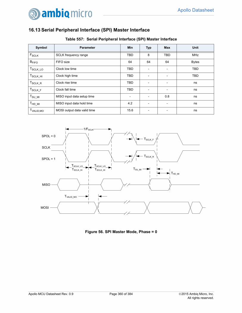
Apollo Datasheet
371
16.13 Serial Peripheral Interface (SPI) Master InterfaceFigure 56. SPI Master Mode, Phase = 0
Table 557: Serial Peripheral Interface (SPI) Master Interface
Symbol Parameter Min Typ Max Unit
FSCLK SCLK frequency range TBD 8 TBD MHz
BFIFO FIFO size 64 64 64 Bytes
TSCLK_LO Clock low time TBD - - TBD
TSCLK_HI Clock high time TBD - - TBD
TSCLK_R Clock rise time TBD - - ns
TSCLK_F Clock fall time TBD - - ns
TSU_MI MISO input data setup time - - 0.8 ns
THD_MI MISO input data hold time 4.2 - - ns
TVALID,MO MOSI output data valid time 15.6 - - ns
SCLK
MISO
THD_MI
TSCLK_LOTSCLK_HI
TSCLK_LOTSCLK_HI
1/FSCLK
TVALID_MO
TSU_MI
SPOL = 0
SPOL = 1
MOSI
TSU_MI
TSCLK_R
TSCLK_F
Apollo MCU Datasheet Rev. 0.9 Page 360 of 384 2015 Ambiq Micro, Inc.All rights reserved.

Apollo Datasheet
371
Figure 57. SPI Master Mode, Phase = 1
SCLK
MISO
THD_MI
TSCLK_LOTSCLK_HI
TSCLK_LOTSCLK_HI
1/FSCLK
TVALID_MO
SPOL = 0
SPOL = 1
MOSI
TSU_MI
TSCLK_R
TSCLK_F
Apollo MCU Datasheet Rev. 0.9 Page 361 of 384 2015 Ambiq Micro, Inc.All rights reserved.

Apollo Datasheet
371
16.14 Serial Peripheral Interface (SPI) Slave InterfaceFigure 58. SPI Slave Mode, Phase = 0
Table 558: Serial Peripheral Interface (SPI) Slave Interface
Symbol Parameter Test Conditions Min Typ Max Unit
FSCLK SCLK frequency range - - 24 MHz
BFIFO FIFO size 64 64 64 Bytes
TSCLK_LO Clock low time TBD - - TBD
TSCLK_HI Clock high time TBD - - TBD
TSCLK_R Clock rise time TBD - - ns
TSCLK_F Clock fall time TBD - - ns
TCE_LEAD Chip enable low to first SCLK edge - - - -
TCE_LAG Chip enable high to last SCLK edge - - - -
TCE_SDO Chip enable low to MISO data output - - - -
TCE_SDZ Chip enable high to MISO data tri-state - - - -
TSU_SI MOSI input data setup time SPOL = 0 - - 0.8 ns
THD_SI MOSI input data hold time SPOL = 0 4.2 - - ns
TVALID,SO MISO output data valid time SPOL = 0 15.6 - - ns
TSU_SI MOSI input data setup time SPOL = 1 - - 0.4 ns
THD_SI MOSI input data hold time SPOL = 1 4.2 - - ns
TVALID,SO MISO output data valid time SPOL = 1 14.8 - - ns
SCLK
MISO
THD_SI
TSCLK_LO
TSCLK_HI
TSCLK_LO
TSCLK_HI
1/FSCLK
THD_SO
TVALID_SO
TSU_MI
SPOL = 0
SPOL = 1
MOSI
TSU_SI
TSCLK_R
TSCLK_F
CE
TCE_SDO
TCE_LEAD TCE_LAG
TCE_SDZ
Apollo MCU Datasheet Rev. 0.9 Page 362 of 384 2015 Ambiq Micro, Inc.All rights reserved.

Apollo Datasheet
371
Figure 59. SPI Slave Mode, Phase = 1
16.15 Universal Asynchronous Receiver/Transmitter (UART)
16.16 Counter/Timer (CTIMER)
Table 559: Universal Asynchronous Receiver/Transmitter (UART)
Symbol Parameter Min Typ Max Unit
FBAUD UART baud rate - - 921600 bps
Table 560: Counter/Timer (CTIMER)
Symbol Parameter Min Typ Max Unit
FCTIMER Input frequency - - 24 MHz
TCTIMER Capture pulse width 100 - - ns
SCLK
MISO
THD_SI
TSCLK_LO
TSCLK_HI
TSCLK_LO
TSCLK_HI
1/FSCLK
THD_SO
TVALID_SO
SPOL = 0
SPOL = 1
MOSI
TSU_SI
TSCLK_R
TSCLK_F
CETCE_LEAD TCE_LAG
TCE_SDO TCE_SDZ
Apollo MCU Datasheet Rev. 0.9 Page 363 of 384 2015 Ambiq Micro, Inc.All rights reserved.

Apollo Datasheet
371
16.17 Flash Memory16.18 General Purpose Input/Output (GPIO)All GPIOs have Schmitt trigger inputs.
Table 561: Flash Memory
Symbol Parameter Min Typ Max Unit
PECYC Program/erase cycles before failure 10K - - cycles
TFDR Data retention 10 - - years
TPAGE_ERASE Single page erase time (2048 bytes) - 40 - ms
TMASS_ERASE Mass erase time - 40 - ms
IPROGRAM Supply current during a page program - 4.3 mA
IERASE Supply current during a page erase - - 3.44 mA
Table 562: General Purpose Input/Output (GPIO)
Symbol Parameter Condition Min Typ Max Unit
All GPIOs
VOH High-level output voltage
3.0 mA load, low drivestrength
0.8 * VDDP -- -- V5.7 mA load, high drivestrength
VOL Low-level output voltage
2.6 mA load, low drivestrength
- - 0.2 * VDDP V5.1mA load, high drivestrength
VIHPositive going input thresholdvoltage
0.61*VDDP - V
VILNegative going input thresholdvoltage
- 0.33*VDDP V
VHYS Input hysteresis 0.225 0.325 0.425 V
CGPI Input capacitance - 3.6 - pF
RPU Pull-up resistance 25 40 180 kΩ
RPD Pull-down resistance 25 65 800 kΩ
RPUI2C00I2C pad pull-up resistance, RSEL = 0x00
- 1.5 - kΩ
RPUI2C01I2C pad pull-up resistance, RSEL = 0x01
- 6 - kΩ
RPUI2C10I2C pad pull-up resistance, RSEL = 0x10
- 12 - kΩ
RPUI2C11I2C pad pull-up resistance, RSEL = 0x11
- 24 - kΩ
IIN Input pin leakage current - 1 20 nA
Apollo MCU Datasheet Rev. 0.9 Page 364 of 384 2015 Ambiq Micro, Inc.All rights reserved.

Apollo Datasheet
371
IINODOpen drain output leakage cur-rent
- 1 20 nA
Standard GPIOs
ISRC_STD Output source currentVDDP = 1.8V, low drivestrength
3 4.4 - mA
ISRC_STD Output source currentVDDP = 1.8V, high drivestrength
5.7 8.4 - mA
ISNK_STD Output sink currentVDDP = 1.8V, low drivestrength
2.6 4 - mA
ISNK_STD Output sink currentVDDP = 1.8V, high drivestrength
5.1 7.7 - mA
Power Switch GPIOs
PWRSOURCE_RESHigh side power switch resis-tance
- 1.3 2 Ω
ISRC_PWRHigh side power switch sourcecurrent
50 - - mA
PWRSINK_RES Low side power switch resistance - 1.3 3 Ω
ISNK_PWRLow side power switch sink cur-rent
50 - - mA
Table 562: General Purpose Input/Output (GPIO)
Apollo MCU Datasheet Rev. 0.9 Page 365 of 384 2015 Ambiq Micro, Inc.All rights reserved.

Apollo Datasheet
371
16.19 Serial Wire Debug (SWD)Figure 60. Serial Wire Debug Timing
Table 563: Serial Wire Debug (SWD)
Symbol Parameter Min Typ Max Unit
TSWDCK_HI SWDCK clock high period 0.085 - 500 µs
TSWDCK_LO SWDCK clock low period 0.085 - 500 µs
TOS_SWD SWDIO output skew to falling edge of SWDCLK -5 - 45 ns
TSU_SWD Input setup time between SWDIO and rising edge SWDCK 65 - - ns
THD_SWD Input hold time between SWDIO and rising edge SWDCK 125 - - ns
StartParityDataDataParkStopDebugger Probe Output to SWDIO High‐Z
Debugger Probe Output to SWDCK
AcknowledgeHigh‐Z High‐Z
TOS_SWD TSWDCK_HI TSWDCK_LO
Read Cycle
Apollo Output to SWDIO
Start
ParityDataData
ParkStopDebugger Probe Output to SWDIO High‐Z
Debugger Probe Output to SWDCK
AcknowledgeHigh‐Z High‐Z
TSU_SWD
TSWDCK_LO
Write Cycle
Apollo Output to SWDIO
Apollo MCU Datasheet Rev. 0.9 Page 366 of 384 2015 Ambiq Micro, Inc.All rights reserved.

Apollo Datasheet
371
16.20 Serial Wire Output (SWO)16.21 Device Errata and Design Considerations
16.21.1 Apollo Device Errata
The section describes silicon errata for the Apollo MCU device related to operating temperature range,IO master functionality, ADC, and the PDR threshold. The errata listed below apply to devices with thefollowing part numbers: APOLLO512-KBR, APOLLO512-KCR, APOLLO256KBR, APOLLO256-KCR,APOLLO128-KBR, APOLLO128-KCR, APOLLO064-KBR, and APOLLO064-KCR.
16.21.1.1 Operating Temperature Range
16.21.1.1.1 Errata Details & Impact
Revision A3 Apollo MCU devices are only guaranteed to operate within the -10°C to 60°C temperaturerange. This range is less than the one shown in the Apollo MCU datasheet of -40°C to 85°C.The reducedrange is required to guarantee operation as process and voltage vary in revision A3, in addition totemperature.
16.21.1.1.2 Workaround
Customers must use Apollo revision A3 within the reduced temperature range of -10°C to 60°C.
16.21.1.1.3 Resolution
A new silicon revision now in production (A4), expands the operating temperature range to the expectedvalues of -40°C to 85°C.
16.21.1.2 IO Master Clock Pin
16.21.1.2.1 Errata Details & Impact
Apollo MCU devices support configuring each of the two IO Master peripherals in either I2C mode or SPImode. When configured in either mode, the device IO masters may experience issues where a transactionis corrupted. The prevalence of this issue depends on a combination of normal device package variation,board trace inductance, capacitive loading of the SCL/SCLK line, and pad drive strength settings.
Under the right conditions, a second clock edge forms on the SCL/SCLK line that is read by the IO Masterperipheral, which puts it in an undetermined state, corrupting a normal transaction.
This errata affects Apollo MCU revision A3, and A4.
Table 564: Serial Wire Output (SWO)
Symbol Description Min Nom Max Unit
FSWO SWO operation frequency TBD - TBD MHz
DCSWO SWO clock duty cycle - TBD - %
TRISE SWO rise time - TBD - TBD
TFALL SWO fall time - TBD - TBD
TSETUP SWO setup time - TBD - TBD
THOLD SWO hold time - TBD - TBD
Apollo MCU Datasheet Rev. 0.9 Page 367 of 384 2015 Ambiq Micro, Inc.All rights reserved.

Apollo Datasheet
371
16.21.1.2.2 WorkaroundTo prevent this issue across all possible board configurations, Ambiq Micro requires that customers place a100 Ω resistor in series with the SCL/SCLK pin. This resistor should be placed close to the Apollo MCUdevice.
16.21.1.3 ADC OPMODE Supply Voltage Dependency
16.21.1.3.1 Errata Details & Impact
The Apollo ADC peripheral includes a mode controller state machine that manages time slot conversions,clock management of the block, and also the power state of its various analog components. The OPMODEbits in the ADC CFG register configure the sample rate mode to be used by the controller. The reset valuefor the OPMODE field is 0x0, which configures a sample rate less than or equal to 125 kSps. A setting of0x02 configures the ADC for it highest sample rate of up to 800 kSps.
When the OPMODE bits configure the ADC for the highest sample rate, and the supply voltage of thedevice is less than 2.0 V, the ADC may not operate correctly.
This errata affects Apollo MCU revision A3, and A4.
16.21.1.3.2 Workaround
Customers must set the OPMODE bits to 0x0 if using the ADC peripheral on Apollo when the supplyvoltage is less than 2.0 V. This setting guarantees proper operation of the ADC, albeit at a lower samplingrate.
16.21.1.4 ADC Trigger 4 Affects Internal Voltage Rails
16.21.1.4.1 Errata Details & Impact
Apollo’s ADC can be triggered from nine different sources, eight of which are GPIOs configured as externaltriggers. Using ADC external trigger 4 (GPIO41), can affect sampling of the VDD input to the ADC due tocoupling of the rising edge of the trigger signal. This coupling results in an offset of the ADC measurementsof VDD, where the resulting output code is lower than expected. This phenomenon only occurs when usingADC external trigger 4.
This errata affects Apollo MCU revision A3, and A4.
16.21.1.4.2 Workaround
Ambiq Micro recommends not using ADC external trigger 4. This functionality of GPIO41 will bedeprecated in the next version of the Apollo datasheet.
16.21.1.5 POR Rising Slew Rate Limitation
16.21.1.5.1 Errata Details & Impact
RevisionA3 Apollo devices require a rising slew rate to be 10 V/s or faster to guarantee that the MCUproperly comes out of the reset condition. A voltage supply ramp rate less than 10 V/s may result in theMCU never coming out of reset.
16.21.1.5.2 Workaround
Customers using revision A3 must ensure a 10 V/s or higher ramp rate on the MCU input power supplypins.
Apollo MCU Datasheet Rev. 0.9 Page 368 of 384 2015 Ambiq Micro, Inc.All rights reserved.

Apollo Datasheet
371
16.21.1.5.3 ResolutionA new silicon revision now in production (A4) corrects this issue, removing any slew rate requirements forthe input supply.
16.21.1.6 Falling POR Threshold At Cold Temperatures
16.21.1.6.1 Errata Details & Impact
Apollo has a falling edge POR (power-on reset) threshold set to approximately 1.72 V, which will safelyreset the MCU state prior to its input power supply falling below the absolute minimum value, which wouldcause functional failures. While operating the ADC peripheral at cold temperatures, between -10°C and-40°C, it’s possible for a system functional failure to occur above this 1.72 V threshold. Operating the ADCat cold temperatures can possibly cause the voltage of an internal supply to drop below 1.72 V, while thesupply coming into the chip remains above the threshold.
This errata affects Apollo MCU revision A3, and A4.
16.21.1.6.2 Workaround
As a result, Ambiq Micro recommends using the BOD (brown-out detection) feature, with a threshold set to2.1 V, to detect a low supply condition at cold temperatures, and disable the ADC in these situations. SeeSection 11.4of the Apollo datasheet for more details on using the BOD monitor to detect brown-out events.
16.21.2 Key Design Guidelines
16.21.2.1 Input Supply Voltage and Rising POR Threshold
The Apollo device is designed to work with input power supplies between 1.8 V and 3.8 V, after a power-on reset condition has been de-asserted. However, to de-assert the power-on reset condition, a supplyvoltage higher than the POR threshold of >2.05 V must be applied to the device for at minimum 100 ms.After that condition is satisfied, system reset is de-asserted and normal MCU operation proceeds.
Typical power supply designs do not allow for a short 100 ms voltage pulse of >2.05 V, followed by asteady-state value of around 1.8 V. Therefore, Ambiq Micro recommends that most customers use avoltage supply at minimum of 2.1 V to power the Apollo MCU, unless such a voltage sequence is possiblein their design.
16.21.2.2 ADC Channel 0 Input Leakage
The Apollo ADC supports 13 user-selectable input channels, eight of which are external GPIO inputs. ADCexternal inputs 1 through 7 have an input leakage current specification of typically 0.1 nA, with a maximumleakage of 20 nA. ADC external input 0 has a much higher input leakage current, typically 5 µA, but as highas 10 µA.
The additional leakage current on external input 0 can create a noticeable offset in ADC samples,depending on the output impedance of the signal source being measured. Customers using externalinput 0 must be aware of this additional leakage and account for it when selecting a signal source to besampled, or use one of the other seven external inputs.
16.21.2.3 32.768 kHz Crystal Considerations
16.21.2.3.1 Crystal Load Capacitors and Frequency Accuracy
The Apollo MCU clock generator module includes a high-precision crystal-controlled oscillator that worksin conjunction with an external 32.768 kHz tuning fork crystal. The crystal oscillator includes a distributed
Apollo MCU Datasheet Rev. 0.9 Page 369 of 384 2015 Ambiq Micro, Inc.All rights reserved.

Apollo Datasheet
371
digital calibration function, that can be used to calibrate the 16 kHz level of the internal MCU clock dividerchain to within ±1 ppm accuracy.The crystal oscillator is designed to run without the use of external load capacitors, and use the digitalcalibration function to create a highly accurate clock for internal use. Not using external load capacitorssignificantly increases oscillator allowance, and allows for a reduction in crystal bias current, which resultsin lower power consumption. Lower power consumption is often most beneficial when the MCU is in deepsleep mode, but needs to keep the crystal oscillator running as an accurate time source for the RTCmodule.
16.21.2.3.2 Replacing Crystal with an XO or TCXO
Due to design requirements, some customers prefer to use an XO (external oscillator) device, or a TCXO(temperature-controlled external oscillator) as a replacement for the 32.768 kHz crystal. The Apollo MCUcrystal oscillator was not originally designed to support these kinds of inputs but can be adapted to workwith them.
The crystal-controlled oscillator circuit expects an input between 150 mVpp and 250 mVpp, with a nominalvalue of 200 mVpp. Typically, XO-type devices have a much higher output voltage, and must be AC-coupled into the Apollo oscillator input. To do so, Ambiq Micro recommends using a capacitive dividerbetween the XO/TCXO output and the XO pin of the device. The XI pin must not be left floating. Instead, a1 nF capacitor should connect the XI pin to the MCU’s ground. See Figure 61 below for an example of acircuit illustrating the recommended connection.
Figure 61. External Oscillator Example Connection
16.21.2.4 Updated DC-DC Converter Requirements
Apollo features two built-in Buck converters optimized for low-power environments, featuring ultra-lowquiescent current and an integrated power switch. Therefore, only an external inductor and capacitor areneeded for each converter to enable very high efficiency power input for the MCU core, SRAM, Flashmemory, analog blocks, and digital logic.
To ensure best performance across process, voltage, and temperature, additional capacitance is neededat the VOUT1 Buck converter output to help reduce ripple. Compared to older Apollo example schematics,the VOUT1 output capacitor must be increased from 1 µF to 2 µF. Using a standard capacitor value of2.2 µF is also acceptable. See Figure 62 below for an updated Buck converter example schematic.
Oscillator Apollo
1 nFXO
XI
CXO2
CXO1
VDDVDD
Apollo MCU Datasheet Rev. 0.9 Page 370 of 384 2015 Ambiq Micro, Inc.All rights reserved.

Apollo Datasheet
371
Figure 62. Updated Buck Converter Schematic, Showing C3 Value as 2.0 µF
VDD4VDDHVSSL
VDDAVSSA
VDDPSW1
VOUT1SW2
VOUT2VSSP
GPIO49GPIO48GPIO47
DIGITAL
ANALOG
BUCK
POWER
VDDHVDD_MCU
VDDA
VDD_MCU
2.2μHC4
1.0 μF
C8H3
R2 0Ω
F2
D6D7
A1B1A2C1D1B2
D3H6G6
M0nCE7_TCTB3_GPIO49M0nCE6_TCTA3_GPIO48M0nCE5_TCTB2_GPIO47
C32.0 μF
2.2μHSW1
VOUT1SW2
VOUT2
L1
L2
Apollo MCU Datasheet Rev. 0.9 Page 371 of 384 2015 Ambiq Micro, Inc.All rights reserved.
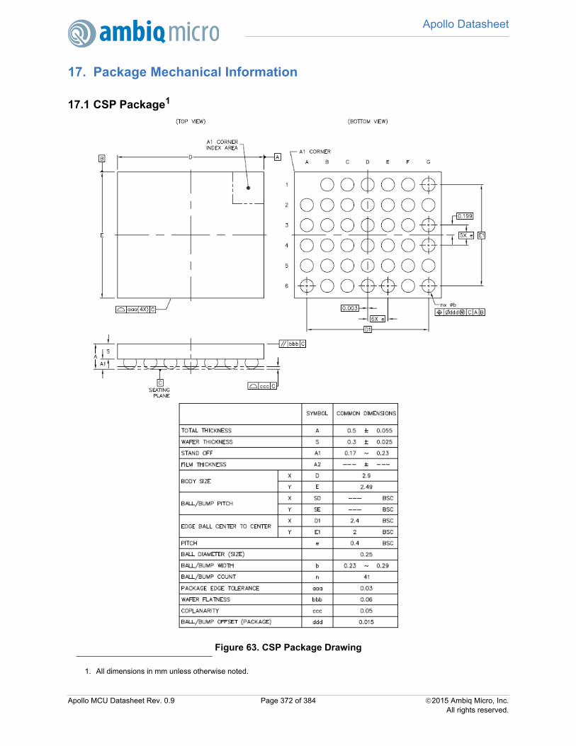
Apollo Datasheet
377
17. Package Mechanical Information
17.1 CSP Package1
Figure 63. CSP Package Drawing
1. All dimensions in mm unless otherwise noted.
Apollo MCU Datasheet Rev. 0.9 Page 372 of 384 2015 Ambiq Micro, Inc.All rights reserved.

Apollo Datasheet
377
17.1.1 PCB land pattern and solder stencilFigure 64. Example PCB Land Pattern for CSP Package
A 4 mil stencil is recommended.
Figure 65. Example Solder Stencil Pattern for CSP Package
ø 0.254
45° x 0.15
0.4
3.10
2.70
0.4
0.25
0.25
0.4
0.4
Apollo MCU Datasheet Rev. 0.9 Page 373 of 384 2015 Ambiq Micro, Inc.All rights reserved.

Apollo Datasheet
377
17.2 BGA package1
1. All dimensions in mm unless otherwise noted.
Apollo MCU Datasheet Rev. 0.9 Page 374 of 384 2015 Ambiq Micro, Inc.All rights reserved.

Apollo Datasheet
377
Drawing Notes:Ball width is measured at maximum solder ball diameter, parallel to seating plane.Seating plane is defined by spherical crowns of solder balls.Parallelism measurement shall exclude effect of mark on top surface of package.
Apollo MCU Datasheet Rev. 0.9 Page 375 of 384 2015 Ambiq Micro, Inc.All rights reserved.

Apollo Datasheet
377
17.2.1 PCB land pattern and solder stencilFigure 66. Example PCB Land Pattern for BGA Package
A 4 mil stencil is recommended.
Figure 67. Example Solder Stencil Pattern for BGA Package
0.5
4.50
4.50
0.5
ø 0.25
0.5
0.5
ø 0.3
Apollo MCU Datasheet Rev. 0.9 Page 376 of 384 2015 Ambiq Micro, Inc.All rights reserved.

Apollo Datasheet
377
17.3 Reflow ProfileFigure 68 illustrates the reflow soldering requirements.Figure 68. Reflow Soldering Diagram
Table 565: Reflow Soldering Requirements (Pb-free assembly)
Profile Feature Requirement
Preheat/SoakTemperature Min (Tsmin)Temperature Max (Tsmax)Time (ts) from (Tsmin to Tsmax)
150°C200°C60-120 seconds
Ramp-up rate (TL to Tp) 3°C/second max.
Liquidous temperature (TL)Time (tL) maintained above TL
217°C60-150 seconds
Peak package body temperature (Tp) 260°C max.
Time (tp) within 5°C of Tp 30 seconds max.
Ramp-down rate (Tp to TL) 6°C/second max.
Time 25°C to peak temperature 8 minutes max.
Apollo MCU Datasheet Rev. 0.9 Page 377 of 384 2015 Ambiq Micro, Inc.All rights reserved.

Apollo Datasheet
Index
Numerics10BIT ............................................................ 9112/24 Hour Mode ........................................ 2433-wire mode .................................................. 94AAccess permissions ...................................... 37ACC_ISR .................................................... 112accumulation control ................................... 312accumulation, automatic ............................. 312ACK .................................................... 91, 115Acknowledge ................................................ 91Active Mode .................................................. 37ADC .......................................... 33, 155, 309ADC Configuration Register ....................... 315ADC_DIV3 .................................................. 310ADC_DIV3_LOAD ...................................... 310ADC_EXT0 ................................................. 310ADC_EXT1 ................................................. 310ADC_EXT2 ................................................. 310ADC_EXT3 ................................................. 310ADC_EXT4 ................................................. 310ADC_EXT5 ................................................. 310ADC_EXT6 ................................................. 310ADC_EXT7 ................................................. 310ADCREF ..................................................... 155ADC_SWT .................................................. 311ADC_TEMP ................................................ 310ADC_TRIG0 ............................................... 310ADC_TRIG1 ............................................... 310ADC_TRIG2 ............................................... 311ADC_TRIG3 ............................................... 311ADC_TRIG5 ............................................... 311ADC_TRIG6 ............................................... 311ADC_TRIG7 ............................................... 311ADC_VDD .................................................. 310ADC_VSS ................................................... 310AHB .................................................... 37, 111Alarm Registers .......................................... 242ALM interrupt .............................................. 242ALM100 ...................................................... 242AM08XX, see real-time clockAM18XX, see real-time clockAMBA ........................................................... 37Analog Multiplexer Channel Selection ........ 312analog mux ................................................. 310analog-to-digital converter ............................ 33APB .............................................................. 37Apollo ............................................................ 32Architecture Reference Manual .................... 38Area, Direct ................................................. 112ARM, see processorARMv7 .......................................................... 37
AtAuAuBBabaBCBuBuBubububububuCCaCACACLClclocloCMCMCMcoCOCocococoCocoCPCPCTCTDDaDCdeDedeDeDeDeDiDiEEGevev
Apollo MCU Datasheet Rev. 0.9 Page
tachment, debugger .................................. 38toadjustment, HFRC .............................. 226tomatic Sample Accumulation ................ 312
ndgap ..................................................... 311ttery life ..................................................... 32D format ................................................. 242ck Converter Charge Insertion ............... 256ck Converters ......................................... 351s Not Busy ...................................... 90, 115s, AMBA AHB ............................................ 37s, AMBA APB ............................................ 37s, DCode .................................................. 37s, ICode .................................................... 37s, System .................................................. 37
libration, Distributed Digital .................... 225LRC ....................................................... 225LXT ........................................................ 225KOUT ................................. 224, 225, 227
ock Generator Module ............................ 224ck sources ................................................ 33ck, interface ............................................. 88POUT .................................................... 344PR0 ............................................. 254, 255PR1 ....................................................... 255
mparator, window ................................... 309NT ........................................................... 93ntinuous ................................................. 255ntrol, accumulation ................................. 312nverters, buck ......................................... 351re, see processorrtex, see processorunter, 32-bit ............................................. 256HA ......................................... 94, 97, 120OL .......................................... 94, 97, 120RERR .................................................... 242S ............................................................ 154
ta Valid ........................................... 90, 115ode .......................................................... 37
bug ........................................................... 38bug Interfaces .......................................... 38bugger attachment ................................... 38ep Sleep ................................................. 225ep Sleep Mode ................................. 37, 38ep Slope Mode ....................................... 120
rect Area .................................................. 112stributed Digital Calibration ..................... 225
_IOSLAVE_FIFOPTR_FIFOSIZ ............ 113ent ............................................................. 33ent, wakeup .............................................. 37
378 of 384 2015 Ambiq Micro, Inc.All rights reserved.

Apollo Datasheet
FFast Mode Plus ........................................... 114fault handler, Memanage .............................. 37Faulting Address Trapping Hardware ........... 39FIFO ................................................. 112, 309
Area Functions ..................................... 113FIFOBASE .................................................. 112FIFOCTR .................................................... 113FIFOMAX .................................................... 112FIFOPTR .................................................... 113FIFOREM ..................................................... 89FIFORTHR ................................................... 90FIFOSIZ .............................................. 89, 113FIFOUPD .................................................... 114FIFOWTHR ................................................... 90flash .............................................................. 33GGPIO ........................................................... 142GPIO and Pad Configuration Module ......... 139GPIOA_IER ................................................ 142GPIOA_ISR ................................................ 142GPIOA_WCR .............................................. 142GPIOB_IER ................................................ 143GPIOB_ISR ................................................ 143GPIOB_WCR .............................................. 143GPIOB_WSR .................................... 142, 143GPIOEN ...................................................... 142GPIOENA ................................................... 142GPIOENB ................................................... 142GPIOnINCFG ................................... 142, 145GPIOn_INT ................................................. 145GPIOnINTD ................................................ 145GPIOnINTP ................................................ 142GPIOnOUTCFG ......................................... 144GPIORD ..................................................... 145GPIORDA ................................................... 142GPIORDB ................................................... 142GPIOWT ........................................... 142, 143GPIOWTA ................................................... 142GPIOWTB ................................................... 142GPIOWTCA ................................................ 142GPIOWTCB ................................................ 142GPIOWTSA ................................................ 142GPIOWTSB ................................................ 142HHardware, Fault Address Trapping ............... 39HFADJ Register .......................................... 235HFADJCK ................................................... 227HFRC ................................................ 226, 310HFRC Autoadjustment ................................ 226HFRCDEL ................................................... 228HFXTADJ .................................................... 226High Frequency RC Oscillator .................... 226HR1224 ...................................................... 243
II2C
I2CI2CICIEInsInsintint
Int
IOIOIOITMLLDLFlifeLoLoMMama
Apollo MCU Datasheet Rev. 0.9 Page
10-bit addressing ................................. 1167-bit addressing ................................... 116ADDRESS .............................................. 91Address ................................................ 116Command .............................................. 91FIFO ....................................................... 89I2CADDR ................................... 114, 116IO Master 0 .......................................... 145IO Master 0 Loopback .......................... 150IO Master 1 .......................................... 146IO Master 1 Loopback .......................... 150IO Slave ............................................... 149master .................................................... 88Multi-master Arbitration .......................... 94Normal Read .......................................... 92Normal Write .......................................... 92Offset Address ............................. 92, 116Raw Read .............................................. 93Raw Write .............................................. 93Read .................................................... 117receiver .................................................. 90SCL ........................................................ 90SDA ....................................................... 90Slave .......................................... 111, 114transmitter .............................................. 90Write ..................................................... 117/SPI Master ........................................... 224/SPI Master Module ................................ 88
ode ............................................................ 37 bit ........................................................... 253trumentation Trace Macrocell .................. 38trumentation Trace Module ...................... 33
erfaces, debug .......................................... 38errupt ................................................ 33, 34
ALM ..................................................... 242IOINT ................................................... 114RDERR ................................................ 114
erruptsVector Table ........................................... 34
Slave Interrupt ....................................... 150INT .......................................................... 114READ ...................................................... 114
, see Instrumentation Trace Macrocell
O ............................................................ 351RC ................................................ 225, 228, battery .................................................... 32opback .................................................... 150w-Power Consumption Modes ................. 33
naged Conversion Slots ........................ 311p, memory ............................................... 35
379 of 384 2015 Ambiq Micro, Inc.All rights reserved.

Apollo Datasheet
Master Module , I2C/SPI .............................. 88MCU, see Apollo<$noage ............................. 32MCU_CTRL ................................................ 228MemManage ................................................. 37memory ......................................................... 33
LRAM ........................................... 89, 111RAM ....................................................... 33SRAM ..................................................... 37
memory map ................................................. 35peripheral device .................................... 36
Memory Protection Unit ................................ 36MISO ............................................................ 94mode
Active ..................................................... 37Deep Sleep .................................. 38, 225Sleep ...................................................... 38
mode, Deep Sleep ........................................ 37Module, ADC and Temperature Sensor ...... 309module, PINCFG .......................................... 94MOSI ............................................................ 94MPU, see Memory Protection Unitmux, analog ................................................ 310NNAK ............................................................ 116Nested Vectored Interrupt Controller ............ 34NSEL .......................................................... 344NVIC, see Nested Vectored Interrupt ControllerOOPER ........................................................... 92oscillator
High Frequency RC .............................. 226high frequency RC ............. 33, 224, 310low frequency RC ............... 33, 224, 225RC .......................................................... 33XTAL .................................. 33, 224, 225XTAL Failure Detection ........................ 228
OUTDATSEL .............................................. 143OUTENSEL ............................ 143, 144, 145PPAD10PULL ............................................... 147PAD16FNCSEL .......................................... 155PAD20FNCSEL .......................................... 156PAD20INPEN ............................................. 156PAD21INPEN ............................................. 156PAD5INPEN ..................................... 145, 146PAD5PULL ....................................... 145, 146PAD5RSEL ................................................. 145PAD6INPEN ..................................... 145, 146PAD6PULL ....................................... 145, 146PAD6RSEL ................................................. 145PAD7PULL ................................................. 146PAD8INPEN ..................................... 146, 147PAD8PULL ....................................... 146, 147PAD9INPEN ..................................... 146, 147
PAPAPAPAPAPAPAPePIpopoPoproPrPrPSPTPWRratRDRereaRERERERERERERERERERERERERERERERERERERERERERERERERERERERERERERE
Apollo MCU Datasheet Rev. 0.9 Page
D9PULL ....................................... 146, 147DKEY ..................................................... 142DnFNCSEL .................. 139–??, 140, 142DnINPEN ........................... 145, 148, 153DnPULL ................... 140, 145, 148, 153DnRSEL ................................................. 145DnSTRNG .............................................. 144ripheral Device Memory Map ................... 36
NCFG ........................................................ 94wer ............................................................ 32wer modes ................................................ 37wer Optimization .................................... 256cessor ...................................................... 33
otected Memory System Architecture ....... 36otection regions ........................................ 36EL .......................................................... 344AT ........................................................... 344DKEY .................................................... 344
e, sampling ............................................. 309ERR ....................................................... 114al Time Clock Module ............................ 227l-time clock .............................................. 33G_CLK_GEN_ALMLOW_ALM100 ........ 242G_CLK_GEN_ALMLOW_ALMHR ......... 242G_CLK_GEN_ALMLOW_ALMMIN ....... 242G_CLK_GEN_ALMLOW_ALMSEC ...... 242G_CLK_GEN_ALMUP_ALMDATE ........ 242G_CLK_GEN_ALMUP_ALMMO ........... 242G_CLK_GEN_ALMUP_ALMWKDY ...... 242G_CLKGEN_CALXT ............................. 225G_CLKGEN_CCTRL_CKEN ................. 227G_CLKGEN_CCTRL_CKSEL ............... 227G_CLK_GEN_CTRLOW_CTR100 ........ 241G_CLK_GEN_CTRLOW_CTRHR ......... 241G_CLK_GEN_CTRLOW_CTRMIN ....... 241G_CLK_GEN_CTRLOW_CTRSEC ...... 241G_CLK_GEN_CTRUP_CB ................... 241G_CLK_GEN_CTRUP_CEB ................. 243G_CLK_GEN_CTRUP_CTRDATE ........ 241G_CLK_GEN_CTRUP_CTRERR ......... 242G_CLK_GEN_CTRUP_CTRMO ........... 241G_CLK_GEN_CTRUP_CTRWKDY ...... 241G_CLK_GEN_CTRUP_CTRYR ............ 241G_CLKGEN_HFADJ_HFADJEN ........... 227G_CLKGEN_HFTUNERB ..................... 227G_CLKGEN_OCTRL_OSEL ....... 225, 228G_CLK_GEN_RTCCTL_HR1224 ......... 243G_CLK_GEN_RTCCTL_RPT ............... 242G_CLK_GEN_RTCCTL_RSTOP .......... 242G_CLK_GEN_RTCCTL_WRTC ............ 242G_CLKGEN_STATUS_OMODE ............ 228G_CLKGEN_STATUS_OSCF ............... 228G_CTIMER_CMPR0 ............................. 253
380 of 384 2015 Ambiq Micro, Inc.All rights reserved.

Apollo Datasheet
REG_CTIMER_CMPR0/1 .......................... 252REG_CTIMER_CTCTRLx_CTRLINKx ....... 256REG_CTIMER_CTCTRLx_TMRxyFN ........ 252REG_CTIMER_TMRxyCLR ....................... 253REG_CTIMER_TMRxyEN .......................... 254REG_CTIMER_TMRxyIE ........................... 254REG_CTIMER_TMRxyPE ................ 253, 254REG_CTIMER_TMRxyPOL ....................... 254REG_GPIO_GPIOCFGy ............................ 142REG_GPIO_GPIOyCFG_GPIOnOUTCFG 142REG_GPIO_PADKEY ................................ 139REG_GPIO_PADREG ................................ 139REG_GPIO_PADREGy_PAD11PWRDN .... 139REG_GPIO_PADREGy_PAD20PULL ........ 139REG_GPIO_PADREGy_PAD3PWRUP ...... 139REG_GPIO_PADREGy_PAD4PWRUP ...... 139REG_GPIO_PADREGy_PADnFNCSEL ..... 139REG_GPIO_PADREGy_PADnINPEN ........ 139REG_GPIO_PADREGy_PADnPULL .......... 139REG_GPIO_PADREGy_PADnSTRNG ...... 139REG_IOMSTRn_CLKCFG_DIV3 ................. 88REG_IOMSTRn_CLKCFG_DIVEN .............. 89REG_IOMSTRn_CLKCFG_FSEL ................ 88REG_IOMSTRn_CLKCFG_LOWPER .......... 89REG_IOMSTRn_CLKCFG_TOTPER ........... 88REG_IOMSTRn_CMD .................................. 89REG_IOMSTRn_FIFOPTR_FIFOREM ........ 89REG_IOMSTRn_FIFOPTR_FIFOSIZ ........... 89REG_IOMSTRn_FIFOTHR_FIFOWTHR ..... 89REG_IOMSTRn_IOMCFG_SPHA ................ 94REG_IOMSTRn_IOMCFG_SPOL ................ 94REG_IOSLAVE_FIFOCFG_FIFOBASE ..... 112REG_IOSLAVE_FIFOCFG_FIFOMAX ....... 112REG_IOSLAVE_FIFOCFG_ROBASE ........ 113REG_IOSLAVE_FIFOCTR ......................... 113REG_IOSLAVE_FIFOPTR_FIFOPTR ........ 113REG_IOSLAVE_FUPD_FIFOUPD ............. 114REG_IOSLAVE_FUPD_IOREAD ............... 114REG_IOSLAVE_IOSCFG_I2CADDR ......... 114REG_IOSLAVE_IOSCFG_LSB .................. 120REG_IOSLAVE_PRENC ............................ 113REG_MCU_CTRL_HFRC_HFRCDEL ....... 228Repeated Count ......................................... 253Repeated Pulse .......................................... 254Reset Module ............................................. 286RESTART ................................................... 115RSTn .......................................................... 286RTC, see real-time clockRTS ............................................................ 154Ssampling rate .............................................. 309SAR, see Successive Approximation RegisterSCR, see System Control RegisterSerial Wire Debug ........................................ 38
SeSinSinSleSLSLSloSPSP
SPSTStSTSTStSuSWSWSWSWSYSyTTeTMTP
Apollo MCU Datasheet Rev. 0.9 Page
rial Wire Debugger ................................... 33gle Count ............................................... 253gle Pulse ............................................... 254ep Mode ........................................ 38, 120EEPONEXIT ............................................ 38OTs ......................................................... 311ts, Mananged Conversion ..................... 311HA ............................................................ 97I ................................................................ 943-wire ................................................... 119CHANNEL .............................................. 94CMD Register ........................................ 94Complex Operations .............................. 96frequency ............................................... 88IO Master 0 3-wire ............................... 148IO Master 0 3-wire Loopback ............... 151IO Master 0 4-wire ............................... 146IO Master 0 4-wire Loopback ............... 151IO Master 1 3-wire ............................... 149IO Master 1 3-wire Loopback ............... 152IO Master 1 4-wire ............................... 147IO Master 1 4-wire Loopback ............... 151IO Slave 3-wire .................................... 149IO Slave 4-wire .................................... 149master .................................................... 88Normal Read .......................................... 95Normal Write .......................................... 94OPER ..................................................... 94Phase ..................................................... 97Polarity ................................................... 97Raw Read .............................................. 96Raw Write .............................................. 95Read .................................................... 119Slave .......................................... 111, 118slave .................................................... 118Slave Addressing ................................... 94Write ..................................................... 118
OL .................................................. 97, 120ART ........................................................ 115art Data Transfer ............................. 90, 115OP .................................................. 93, 115OP condition ............................................ 90
op Data Transfer ............................. 90, 115ccessive Approximation Register ... 33, 309D, see Serial Wire DebugD, see Serial Wire DebuggerDCK ...................................................... 156DIO ....................................................... 156SRESETREQn ...................................... 286stem Control Register .............................. 37
mperature Sensor ................................... 309RWCR ......................................... 253, 254IU, see Trace Port Interface Unit
381 of 384 2015 Ambiq Micro, Inc.All rights reserved.

Apollo Datasheet
Trace Port Interface Unit ....................... 33, 38Track and Hold Time ................................... 312TRIGSEL .................................................... 311TX ............................................................... 153UUART ................................................ 153, 226
CTS ...................................................... 154RTS ...................................................... 154RX ........................................................ 153
UPLNGTH .................................................... 94VVCOMP, see Voltage ComparatorVEXT1 ........................................................ 344VEXT2 ........................................................ 344Voltage Comparator .......................... 156, 344Voltage Regulator Module .......................... 351VREFEXT1 ................................................. 344VREFEXT2 ................................................. 344VREFEXT3 ................................................. 344VREFINT .................................................... 344VTEMP ....................................................... 344WWait-For-Interrupt ......................................... 38Wakeup ....................................................... 120wake-up ........................................................ 33Wake-Up Interrupt Controller ........................ 37Watchdog Timer .......................................... 280WC bit ......................................................... 253WDTCFG .................................................... 280WFI, see Wait-For-InterruptWIC, see wake-upWindow comparator .................................... 309Window Comparisons ................................. 312XXT ..................................................... 225, 227XT Oscillator ............................................... 225
Apollo MCU Datasheet Rev. 0.9 Page
382 of 384 2015 Ambiq Micro, Inc.All rights reserved.
Apollo Datasheet
384
18. Ordering Information
19. Document Revision History
Table 566: Ordering Information
Orderable Part Number
Flash RAM Packagea,b
a. For 41-pin WLCSP, minimum order quantity of 5,000 pieces. For 64-pin BGA, minimum order quantity of 4,000 pieces.
b. Compliant and certified with the current RoHS requirements for all 6 substances, including the requirement that lead not exceed 0.1% by weight in raw homogeneous materials. The package was designed to be soldered at high temperatures (per reflow profile) and can be used in specified lead-free processes.
PackingTemperature
Rangec
c. Temperature Range is guaranteed -40 to +85°C by design. Current production test limits are -10 to +60°C
Availability
APOLLO512-KCR 512 KB 64 KB 41-pin WLCSP Tape and Reel -40 to +85°C Now
APOLLO512-KBR 512 KB 64 KB 64-pin BGA Tape and Reel -40 to +85°C Now
APOLLO256-KCR 256 KB 32 KB 41-pin WLCSP Tape and Reel -40 to +85°C 4Q15
APOLLO256-KBR 256 KB 32 KB 64-pin BGA Tape and Reel -40 to +85°C 4Q15
APOLLO128-KCR 128 KB 32 KB 41-pin WLCSP Tape and Reel -40 to +85°C 4Q15
APOLLO128-KBR 128 KB 32 KB 64-pin BGA Tape and Reel -40 to +85°C 4Q15
APOLLO064-KCR 64 KB 16 KB 41-pin WLCSP Tape and Reel -40 to +85°C 4Q15
APOLLO064-KBR 64 KB 16 KB 64-pin BGA Tape and Reel -40 to +85°C 4Q15
Table 567: Document Revision History
Revision Date Description
0.1 December 2014 Initial version
0.2 February 2015 Initial preliminary version
0.3 March 2015 Added register descriptions
0.4 July 2015 Added Host Side Address Space and Register section, Ordering Information
0.45 September 2015Footnote c added to Ordering Information, ADC sample time information updated, changed3.0V spec for current consumption to 3.3V
0.9 February 2016Electrical specifications updated with production values. Several grammatical updates, anddetails added to peripheral functional descriptions.
Apollo MCU Datasheet Rev. 0.9 Page 383 of 384 2015 Ambiq Micro, Inc.All rights reserved.

Apollo Datasheet
384
Contact Information
Address Ambiq Micro, Inc.
6500 River Place Blvd.
Building 7, Suite 200
Austin, TX 78730-1156
Phone +1 (512) 394-8542
Website http://www.ambiqmicro.com/
General Information [email protected]
Sales [email protected]
Technical Support [email protected]
Legal Information and DisclaimersAMBIQ MICRO INTENDS FOR THE CONTENT CONTAINED IN THE DOCUMENT TO BE ACCURATE AND RELIABLE. THIS CONTENT MAY, HOW-EVER, CONTAIN TECHNICAL INACCURACIES, TYPOGRAPHICAL ERRORS OR OTHER MISTAKES. AMBIQ MICRO MAY MAKE CORRECTIONSOR OTHER CHANGES TO THIS CONTENT AT ANY TIME. AMBIQ MICRO AND ITS SUPPLIERS RESERVE THE RIGHT TO MAKE CORRECTIONS,MODIFICATIONS, ENHANCEMENTS, IMPROVEMENTS AND OTHER CHANGES TO ITS PRODUCTS, PROGRAMS AND SERVICES AT ANY TIMEOR TO DISCONTINUE ANY PRODUCTS, PROGRAMS, OR SERVICES WITHOUT NOTICE.
THE CONTENT IN THIS DOCUMENT IS PROVIDED "AS IS". AMBIQ MICRO AND ITS RESPECTIVE SUPPLIERS MAKE NO REPRESENTATIONSABOUT THE SUITABILITY OF THIS CONTENT FOR ANY PURPOSE AND DISCLAIM ALL WARRANTIES AND CONDITIONS WITH REGARD TOTHIS CONTENT, INCLUDING BUT NOT LIMITED TO, ALL IMPLIED WARRANTIES AND CONDITIONS OF MERCHANTABILITY, FITNESS FOR APARTICULAR PURPOSE, TITLE AND NON-INFRINGEMENT OF ANY THIRD PARTY INTELLECTUAL PROPERTY RIGHT.
AMBIQ MICRO DOES NOT WARRANT OR REPRESENT THAT ANY LICENSE, EITHER EXPRESS OR IMPLIED, IS GRANTED UNDER ANY PAT-ENT RIGHT, COPYRIGHT, MASK WORK RIGHT, OR OTHER INTELLECTUAL PROPERTY RIGHT OF AMBIQ MICRO COVERING OR RELATING TOTHIS CONTENT OR ANY COMBINATION, MACHINE, OR PROCESS TO WHICH THIS CONTENT RELATE OR WITH WHICH THIS CONTENT MAYBE USED.
USE OF THE INFORMATION IN THIS DOCUMENT MAY REQUIRE A LICENSE FROM A THIRD PARTY UNDER THE PATENTS OR OTHER INTEL-LECTUAL PROPERTY OF THAT THIRD PARTY, OR A LICENSE FROM AMBIQ MICRO UNDER THE PATENTS OR OTHER INTELLECTUAL PROP-ERTY OF AMBIQ MICRO.
INFORMATION IN THIS DOCUMENT IS PROVIDED SOLELY TO ENABLE SYSTEM AND SOFTWARE IMPLEMENTERS TO USE AMBIQ MICROPRODUCTS. THERE ARE NO EXPRESS OR IMPLIED COPYRIGHT LICENSES GRANTED HEREUNDER TO DESIGN OR FABRICATE ANY INTE-GRATED CIRCUITS OR INTEGRATED CIRCUITS BASED ON THE INFORMATION IN THIS DOCUMENT. AMBIQ MICRO RESERVES THE RIGHTTO MAKE CHANGES WITHOUT FURTHER NOTICE TO ANY PRODUCTS HEREIN. AMBIQ MICRO MAKES NO WARRANTY, REPRESENTATIONOR GUARANTEE REGARDING THE SUITABILITY OF ITS PRODUCTS FOR ANY PARTICULAR PURPOSE, NOR DOES AMBIQ MICRO ASSUMEANY LIABILITY ARISING OUT OF THE APPLICATION OR USE OF ANY PRODUCT OR CIRCUIT, AND SPECIFICALLY DISCLAIMS ANY AND ALLLIABILITY, INCLUDING WITHOUT LIMITATION CONSEQUENTIAL OR INCIDENTAL DAMAGES. “TYPICAL” PARAMETERS WHICH MAY BE PRO-VIDED IN AMBIQ MICRO DATA SHEETS AND/OR SPECIFICATIONS CAN AND DO VARY IN DIFFERENT APPLICATIONS AND ACTUAL PERFOR-MANCE MAY VARY OVER TIME. ALL OPERATING PARAMETERS, INCLUDING “TYPICALS” MUST BE VALIDATED FOR EACH CUSTOMERAPPLICATION BY CUSTOMER’S TECHNICAL EXPERTS. AMBIQ MICRO DOES NOT CONVEY ANY LICENSE UNDER NEITHER ITS PATENTRIGHTS NOR THE RIGHTS OF OTHERS. AMBIQ MICRO PRODUCTS ARE NOT DESIGNED, INTENDED, OR AUTHORIZED FOR USE AS COMPO-NENTS IN SYSTEMS INTENDED FOR SURGICAL IMPLANT INTO THE BODY, OR OTHER APPLICATIONS INTENDED TO SUPPORT OR SUSTAINLIFE, OR FOR ANY OTHER APPLICATION IN WHICH THE FAILURE OF THE AMBIQ MICRO PRODUCT COULD CREATE A SITUATION WHEREPERSONAL INJURY OR DEATH MAY OCCUR. SHOULD BUYER PURCHASE OR USE AMBIQ MICRO PRODUCTS FOR ANY SUCH UNINTENDEDOR UNAUTHORIZED APPLICATION, BUYER SHALL INDEMNIFY AND HOLD AMBIQ MICRO AND ITS OFFICERS, EMPLOYEES, SUBSIDIARIES,AFFILIATES, AND DISTRIBUTORS HARMLESS AGAINST ALL CLAIMS, COSTS, DAMAGES, AND EXPENSES, AND REASONABLE ATTORNEYFEES ARISING OUT OF, DIRECTLY OR INDIRECTLY, ANY CLAIM OF PERSONAL INJURY OR DEATH ASSOCIATED WITH SUCH UNINTENDEDOR UNAUTHORIZED USE, EVEN IF SUCH CLAIM ALLEGES THAT AMBIQ MICRO WAS NEGLIGENT REGARDING THE DESIGN OR MANUFAC-TURE OF THE PART.
Apollo MCU Datasheet Rev. 0.9 Page 384 of 384 2015 Ambiq Micro, Inc.All rights reserved.