Deposition and Patterning Techniques for Organic...
42
Deposition and Patterning Techniques for Organic Materials Andrea Grimoldi Organic Electronics: principles, devices and applications Milano, November 24 th , 2015
Transcript of Deposition and Patterning Techniques for Organic...
Deposition and Patterning
Techniques for Organic Materials
Andrea Grimoldi
Organic Electronics: principles, devices and applications Milano, November 24th, 2015
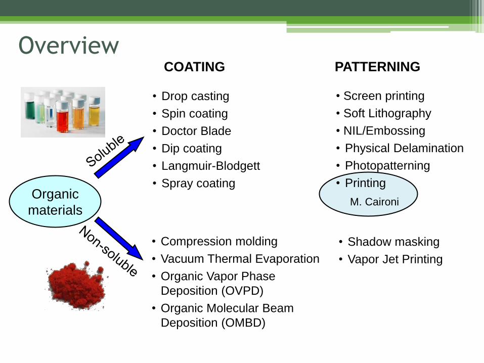
M. Caironi
Overview
Organic
materials
COATING PATTERNING
• Drop casting
• Spin coating
• Doctor Blade
• Dip coating
• Langmuir-Blodgett
• Spray coating
• Screen printing
• Soft Lithography
• NIL/Embossing
• Physical Delamination
• Photopatterning
• Printing
• Compression molding
• Vacuum Thermal Evaporation
• Organic Vapor Phase
Deposition (OVPD)
• Organic Molecular Beam
Deposition (OMBD)
• Shadow masking
• Vapor Jet Printing
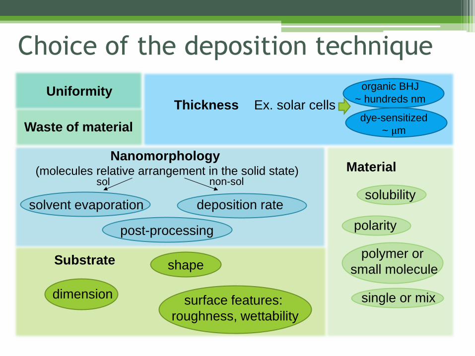
Choice of the deposition technique
Thickness Uniformity
Nanomorphology (molecules relative arrangement in the solid state)
solvent evaporation deposition rate
post-processing
Waste of material
Substrate
dimension surface features:
roughness, wettability
shape
Ex. solar cells
organic BHJ
~ hundreds nm
dye-sensitized
~ μm
sol non-sol
Material
solubility
polarity
single or mix
polymer or
small molecule
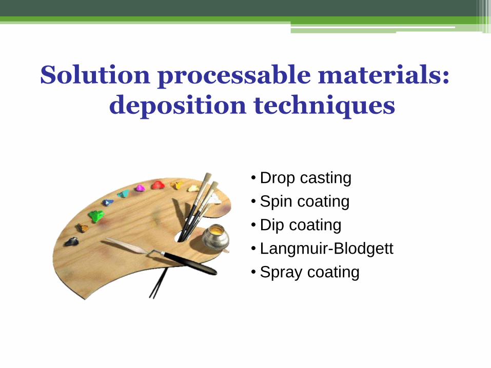
Solution processable materials: deposition techniques
• Drop casting
• Spin coating
• Dip coating
• Langmuir-Blodgett
• Spray coating
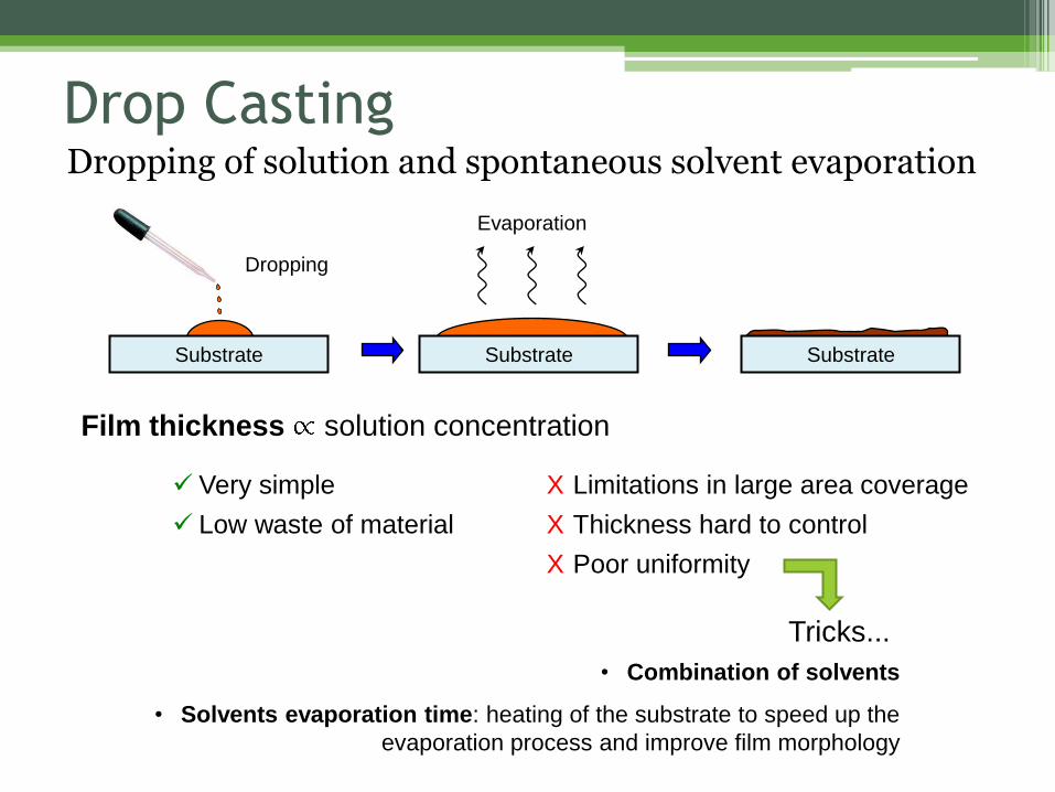
Drop Casting Dropping of solution and spontaneous solvent evaporation
Very simple
Low waste of material
• Combination of solvents
• Solvents evaporation time: heating of the substrate to speed up the
evaporation process and improve film morphology
X Limitations in large area coverage
X Thickness hard to control
X Poor uniformity
Film thickness solution concentration
Tricks...
Substrate
Dropping
Evaporation
Substrate Substrate
Spin Coating I Dropping on spinning substrate
Good uniformity
Reproducibility
Good control on thickness
down of 10nm or less
X Waste of material
X No large area
X Film dries fast less time for molecular ordering
Film thickness: dependent on many controllable
parameters dω/dt, ω, t, solution viscosity,… substrate
Tricks...
•Solvent evaporation time
•Additives
POST-PROCESSING
•Thermal annealing
•Vapor annealing
McCulloch et Al.,
Nat. Mater., 5, 328, (2006) 180ºC
Chang et Al.
Chem. Mater.,16, 23, (2004) P3HT-based TFTs
larger crystallinity
Y. Wang, J. Solar Energ. Eng., 2012, 134, 011017
Z. Zhao et al., Microel. Realiab., 2013, 53, 123
L.M. Chen et al., Adv. Mater., 2009, 21, 1434
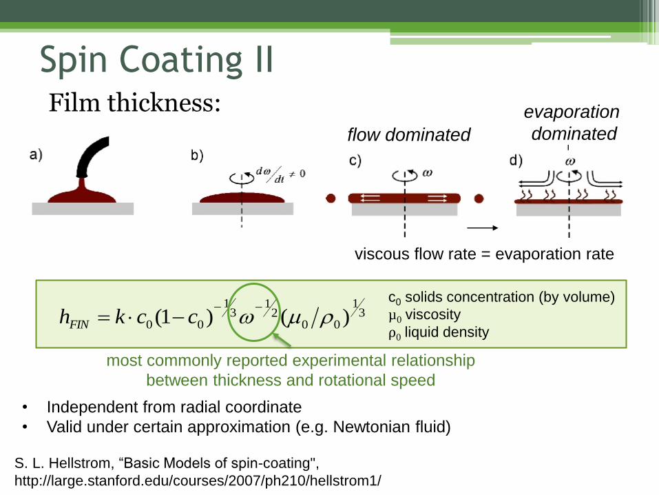
Film thickness:
Spin Coating II
viscous flow rate = evaporation rate
c0 solids concentration (by volume)
µ0 viscosity
ρ0 liquid density
31
002
13
1
00 )()1(
cckhFIN
most commonly reported experimental relationship
between thickness and rotational speed
flow dominated
evaporation
dominated
S. L. Hellstrom, “Basic Models of spin-coating",
http://large.stanford.edu/courses/2007/ph210/hellstrom1/
• Independent from radial coordinate
• Valid under certain approximation (e.g. Newtonian fluid)
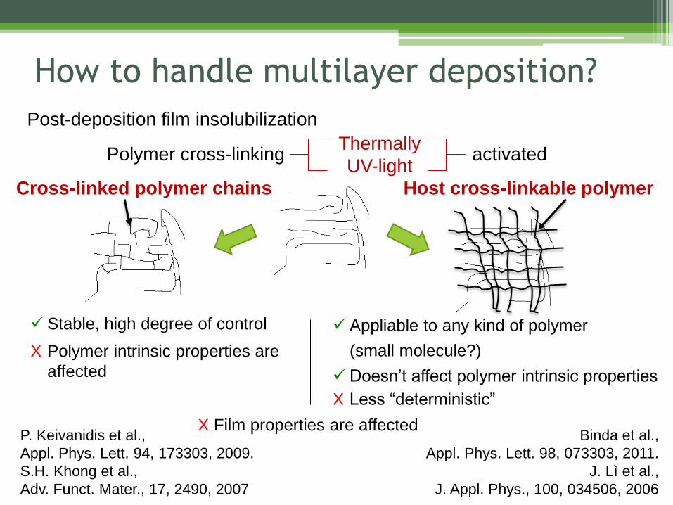
How to handle multilayer deposition?
Post-deposition film insolubilization
Thermally
UV-light activated Polymer cross-linking
Host cross-linkable polymer Cross-linked polymer chains
Stable, high degree of control Appliable to any kind of polymer
(small molecule?)
Doesn’t affect polymer intrinsic properties
X Polymer intrinsic properties are
affected
X Less “deterministic”
X Film properties are affected P. Keivanidis et al.,
Appl. Phys. Lett. 94, 173303, 2009.
S.H. Khong et al.,
Adv. Funct. Mater., 17, 2490, 2007
Binda et al.,
Appl. Phys. Lett. 98, 073303, 2011.
J. Lì et al.,
J. Appl. Phys., 100, 034506, 2006
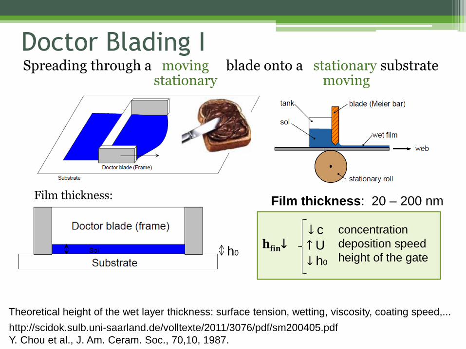
Doctor Blading I Spreading through a moving blade onto a stationary substrate
stationary moving
h0
Film thickness:
Theoretical height of the wet layer thickness: surface tension, wetting, viscosity, coating speed,...
concentration
deposition speed
height of the gate
Film thickness: 20 – 200 nm
↓ c
↑ U
↓ h0
http://scidok.sulb.uni-saarland.de/volltexte/2011/3076/pdf/sm200405.pdf
Y. Chou et al., J. Am. Ceram. Soc., 70,10, 1987.
hfin↓
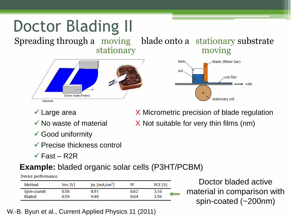
Doctor Blading II
Large area
No waste of material
Good uniformity
Precise thickness control
Fast – R2R
X Micrometric precision of blade regulation
X Not suitable for very thin films (nm)
Example: bladed organic solar cells (P3HT/PCBM)
Doctor bladed active
material in comparison with
spin-coated (~200nm)
Spreading through a moving blade onto a stationary substrate stationary moving
W.-B. Byun et al., Current Applied Physics 11 (2011)
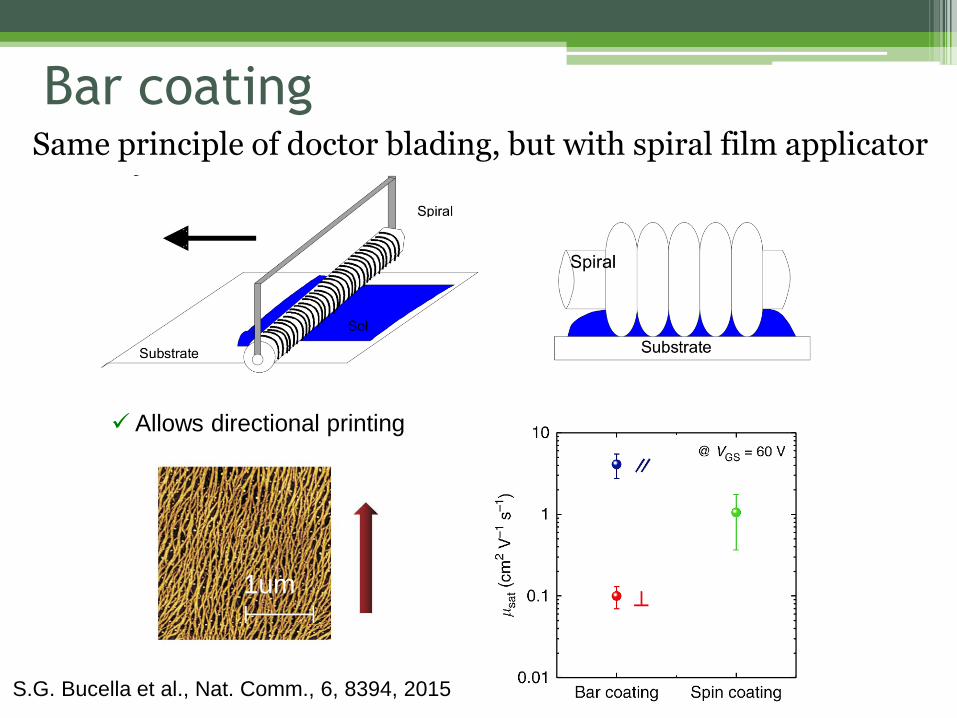
Bar coating Same principle of doctor blading, but with spiral film applicator
S.G. Bucella et al., Nat. Comm., 6, 8394, 2015
1um
Allows directional printing
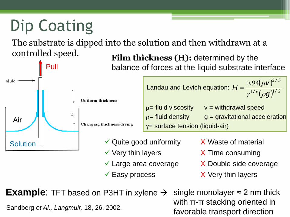
Dip Coating The substrate is dipped into the solution and then withdrawn at a controlled speed.
Solution
Film thickness (H): determined by the
balance of forces at the liquid-substrate interface
Landau and Levich equation:
2161
32940
//
/
g
v.H
= fluid viscosity v = withdrawal speed
= fluid density g = gravitational acceleration
= surface tension (liquid-air)
Quite good uniformity
Very thin layers
Large area coverage
Easy process
X Waste of material
X Time consuming
X Double side coverage
X Very thin layers
Sandberg et Al., Langmuir, 18, 26, 2002.
Example: TFT based on P3HT in xylene single monolayer ≈ 2 nm thick
with π-π stacking oriented in
favorable transport direction
Pull
Air
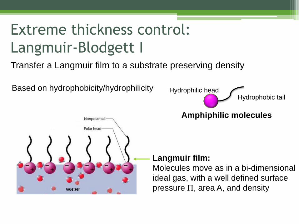
water
Langmuir film:
Molecules move as in a bi-dimensional
ideal gas, with a well defined surface
pressure P, area A, and density
Based on hydrophobicity/hydrophilicity
Extreme thickness control:
Langmuir-Blodgett I
Amphiphilic molecules
Hydrophilic head Hydrophobic tail
Transfer a Langmuir film to a substrate preserving density
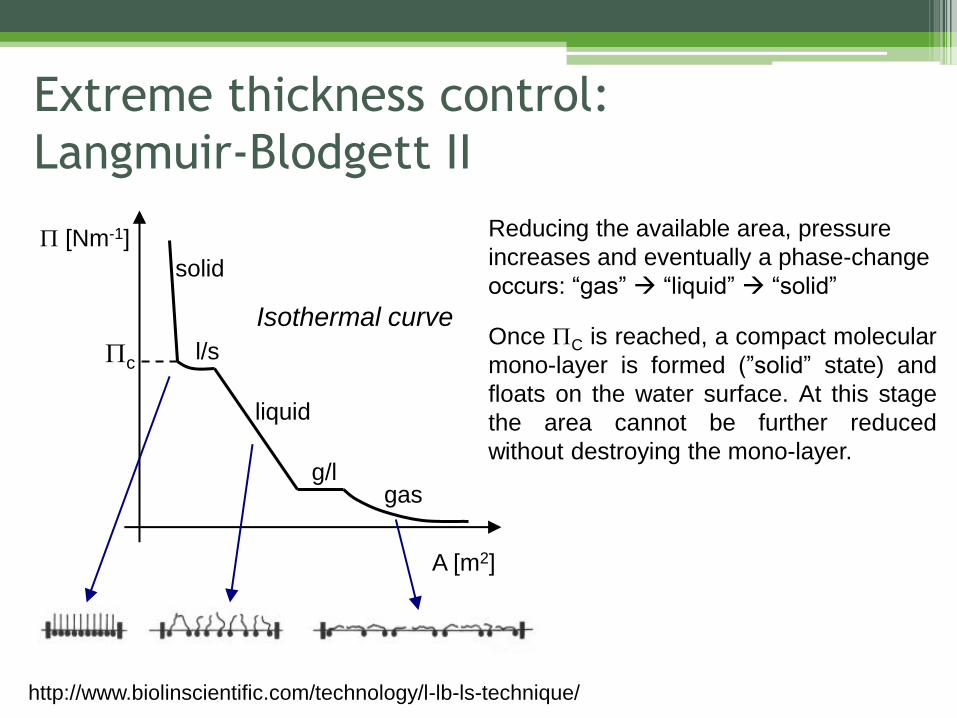
Extreme thickness control:
Langmuir-Blodgett II
Reducing the available area, pressure
increases and eventually a phase-change
occurs: “gas” “liquid” “solid”
A [m2]
P [Nm-1]
gas
liquid
solid
g/l
l/s Pc
Once PC is reached, a compact molecular
mono-layer is formed (”solid” state) and
floats on the water surface. At this stage
the area cannot be further reduced
without destroying the mono-layer.
http://www.biolinscientific.com/technology/l-lb-ls-technique/
Isothermal curve
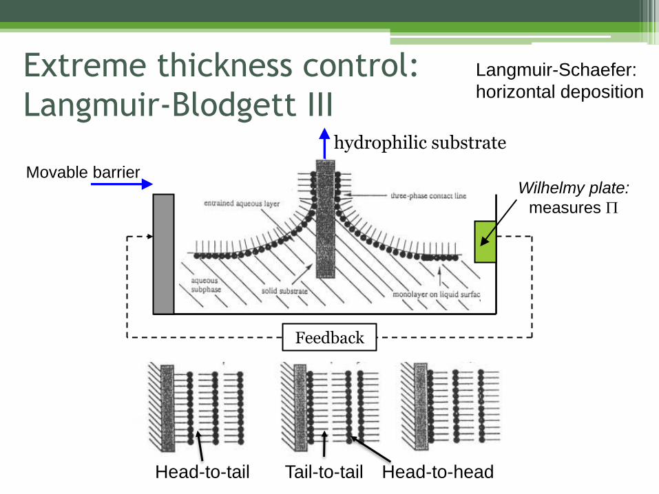
hydrophilic substrate
Movable barrier Wilhelmy plate:
measures P
Feedback
Extreme thickness control:
Langmuir-Blodgett III
Head-to-tail Head-to-head Tail-to-tail
Langmuir-Schaefer:
horizontal deposition
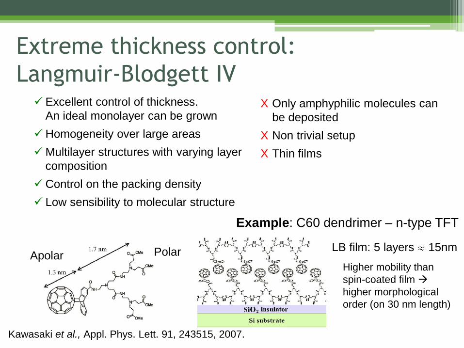
Example: C60 dendrimer – n-type TFT
LB film: 5 layers 15nm Apolar Polar
Kawasaki et al., Appl. Phys. Lett. 91, 243515, 2007.
Higher mobility than
spin-coated film
higher morphological
order (on 30 nm length)
Extreme thickness control:
Langmuir-Blodgett IV Excellent control of thickness.
An ideal monolayer can be grown
Homogeneity over large areas
Multilayer structures with varying layer
composition
Control on the packing density
Low sensibility to molecular structure
X Only amphyphilic molecules can
be deposited
X Non trivial setup
X Thin films
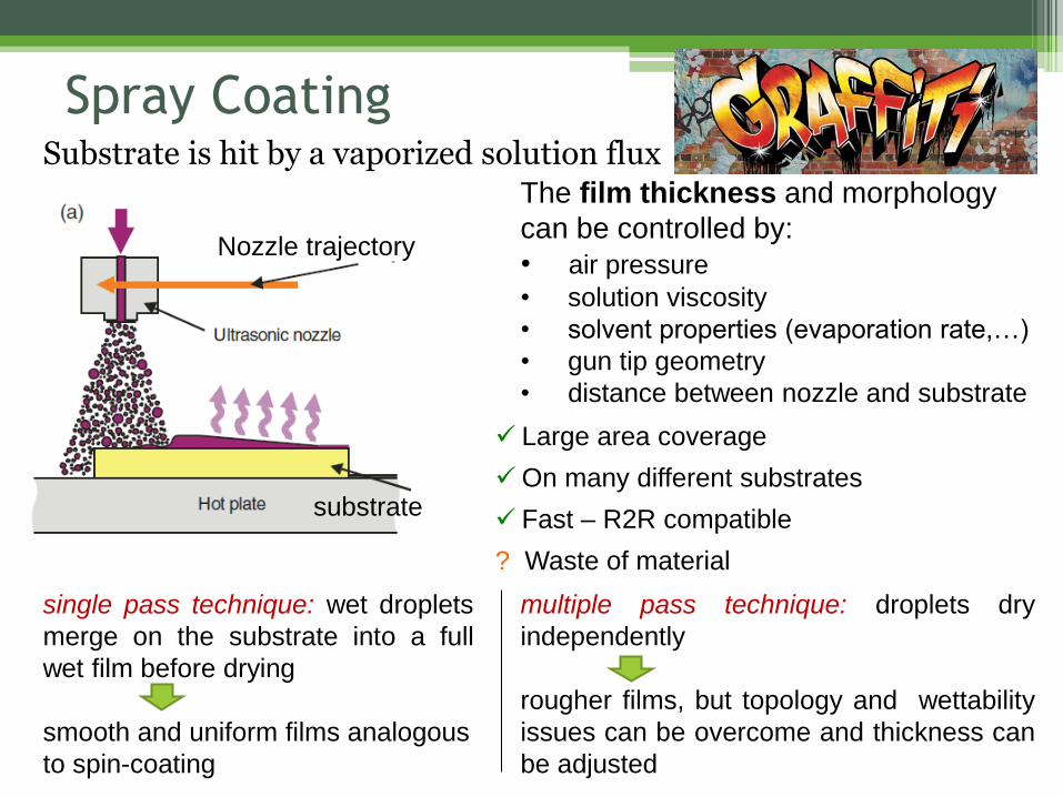
Spray Coating
single pass technique: wet droplets
merge on the substrate into a full
wet film before drying
smooth and uniform films analogous
to spin-coating
The film thickness and morphology
can be controlled by:
• air pressure
• solution viscosity
• solvent properties (evaporation rate,…)
• gun tip geometry
• distance between nozzle and substrate
Substrate is hit by a vaporized solution flux
multiple pass technique: droplets dry
independently
rougher films, but topology and wettability
issues can be overcome and thickness can
be adjusted
substrate
Nozzle trajectory
Large area coverage
On many different substrates
Fast – R2R compatible
? Waste of material
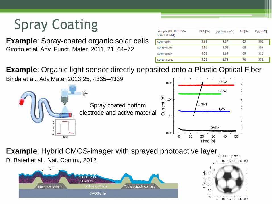
Spray Coating Example: Spray-coated organic solar cells
Example: Organic light sensor directly deposited onto a Plastic Optical Fiber
0 10 20 30 40 50100p
1n
10n
100n
Cu
rren
t [A
]
Time [s]
DARK
LIGHT
1mW
10W
1WSpray coated bottom
electrode and active material
Binda et al., Adv.Mater.2013,25, 4335–4339
Girotto et al. Adv. Funct. Mater. 2011, 21, 64–72
Example: Hybrid CMOS-imager with sprayed photoactive layer D. Baierl et al., Nat. Comm., 2012
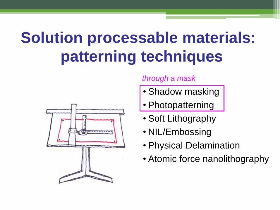
Solution processable materials:
patterning techniques
• Shadow masking
• Photopatterning
• Soft Lithography
• NIL/Embossing
• Physical Delamination
• Atomic force nanolithography
through a mask
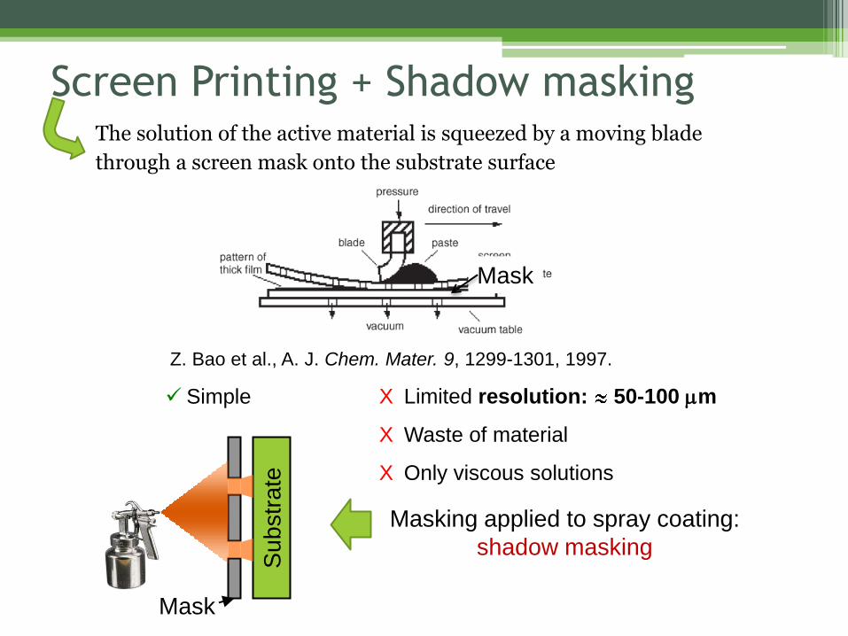
Screen Printing + Shadow masking The solution of the active material is squeezed by a moving blade
through a screen mask onto the substrate surface
Mask
Su
bstr
ate
Masking applied to spray coating:
shadow masking
X Limited resolution: 50-100 m
X Waste of material
X Only viscous solutions
Simple
Mask
Z. Bao et al., A. J. Chem. Mater. 9, 1299-1301, 1997.
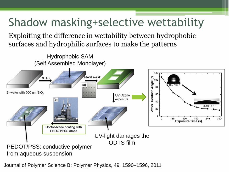
Shadow masking+selective wettability Exploiting the difference in wettability between hydrophobic surfaces and hydrophilic surfaces to make the patterns
UV-light damages the
ODTS film
Journal of Polymer Science B: Polymer Physics, 49, 1590–1596, 2011
PEDOT/PSS: conductive polymer
from aqueous suspension
Hydrophobic SAM
(Self Assembled Monolayer)
Journal of Polymer Science B: Polymer Physics, 49, 1590–1596, 2011
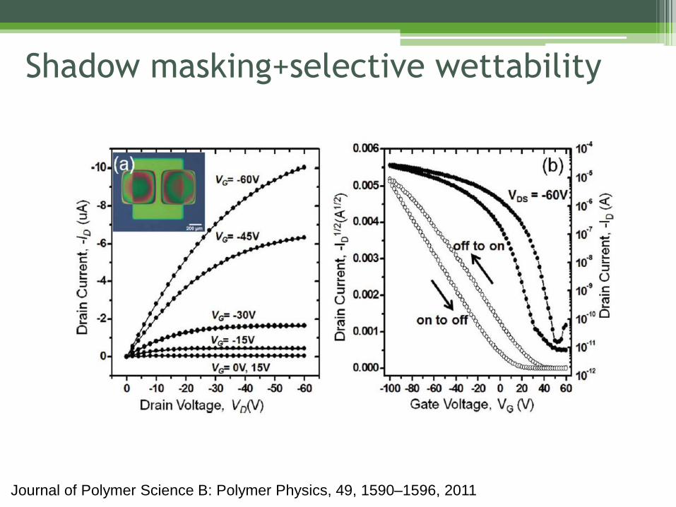
Shadow masking+selective wettability
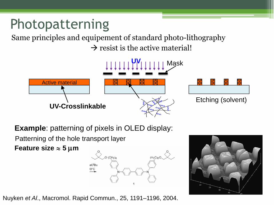
Photopatterning Same principles and equipement of standard photo-lithography
resist is the active material!
Example: patterning of pixels in OLED display:
Nuyken et Al., Macromol. Rapid Commun., 25, 1191–1196, 2004.
Patterning of the hole transport layer
Feature size 5 m
Active material
UV-Crosslinkable
UV Mask
Etching (solvent)
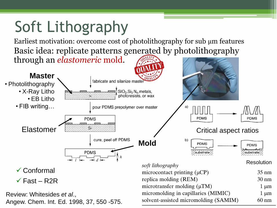
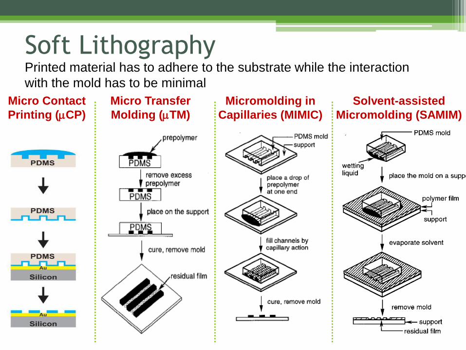
Soft Lithography Earliest motivation: overcome cost of photolithography for sub μm features
Basic idea: replicate patterns generated by photolithography through an elastomeric mold.
Master • Photolithography
• X-Ray Litho
• EB Litho
• FIB writing…
Mold
Elastomer
Review: Whitesides et al.,
Angew. Chem. Int. Ed. 1998, 37, 550 -575.
Critical aspect ratios
Conformal
Fast – R2R
Resolution
Micromolding in
Capillaries (MIMIC)
Soft Lithography Printed material has to adhere to the substrate while the interaction
with the mold has to be minimal
Micro Contact
Printing (CP)
Micro Transfer
Molding (TM)
Solvent-assisted
Micromolding (SAMIM)
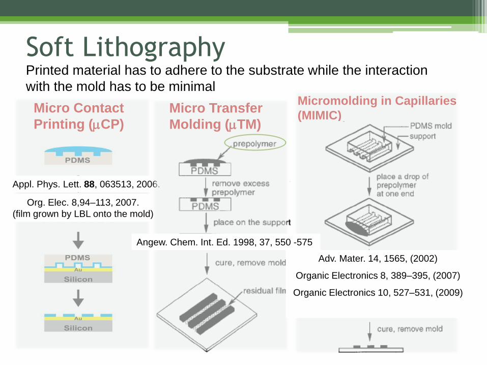
Micromolding in Capillaries
(MIMIC)
Soft Lithography Printed material has to adhere to the substrate while the interaction
with the mold has to be minimal
Micro Contact
Printing (CP)
Micro Transfer
Molding (TM)
Appl. Phys. Lett. 88, 063513, 2006.
Org. Elec. 8,94–113, 2007.
(film grown by LBL onto the mold)
Angew. Chem. Int. Ed. 1998, 37, 550 -575
Adv. Mater. 14, 1565, (2002)
Organic Electronics 8, 389–395, (2007)
Organic Electronics 10, 527–531, (2009)
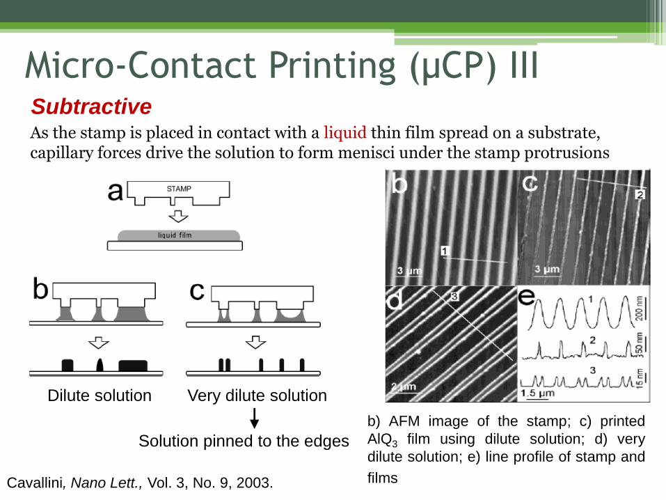
Micro-Contact Printing (µCP) III Subtractive As the stamp is placed in contact with a liquid thin film spread on a substrate, capillary forces drive the solution to form menisci under the stamp protrusions
Dilute solution Very dilute solution
Solution pinned to the edges
b) AFM image of the stamp; c) printed
AlQ3 film using dilute solution; d) very
dilute solution; e) line profile of stamp and
films Cavallini, Nano Lett., Vol. 3, No. 9, 2003.
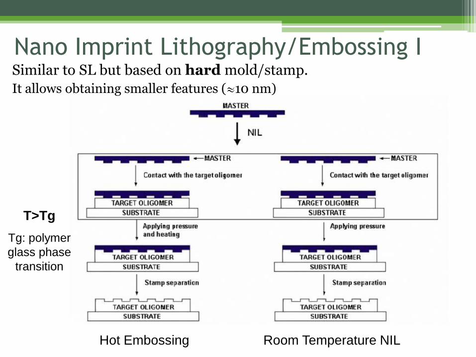
Nano Imprint Lithography/Embossing I Similar to SL but based on hard mold/stamp.
It allows obtaining smaller features ( 10 nm)
Hot Embossing Room Temperature NIL
T>Tg
Tg: polymer
glass phase
transition
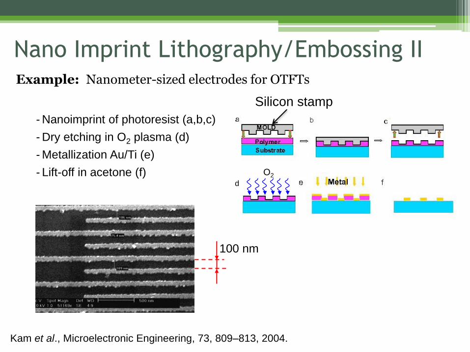
Example: Nanometer-sized electrodes for OTFTs
- Nanoimprint of photoresist (a,b,c)
- Dry etching in O2 plasma (d)
- Metallization Au/Ti (e)
- Lift-off in acetone (f) d
O2
100 nm
Kam et al., Microelectronic Engineering, 73, 809–813, 2004.
Nano Imprint Lithography/Embossing II
Silicon stamp
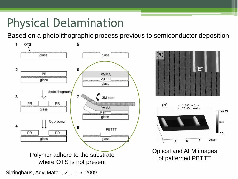
Physical Delamination Based on a photolithographic process previous to semiconductor deposition
Polymer adhere to the substrate
where OTS is not present
Optical and AFM images
of patterned PBTTT
Sirringhaus, Adv. Mater., 21, 1–6, 2009.
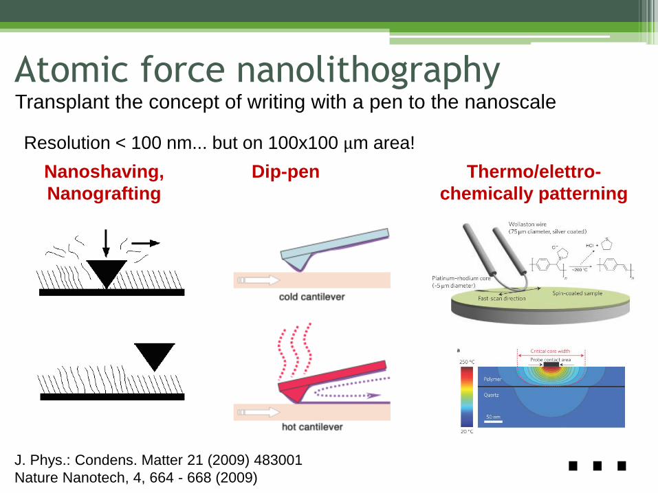
Atomic force nanolithography
Dip-pen
Resolution < 100 nm... but on 100x100 μm area!
Nanoshaving,
Nanografting
J. Phys.: Condens. Matter 21 (2009) 483001
Nature Nanotech, 4, 664 - 668 (2009) ...
Transplant the concept of writing with a pen to the nanoscale
Thermo/elettro-
chemically patterning
Non-soluble materials: deposition techniques
• Vacuum Thermal Evaporation
• Organic Vapor Phase
Deposition (OVPD)
• Organic Molecular Beam
Deposition (OMBD)
• Compression molding
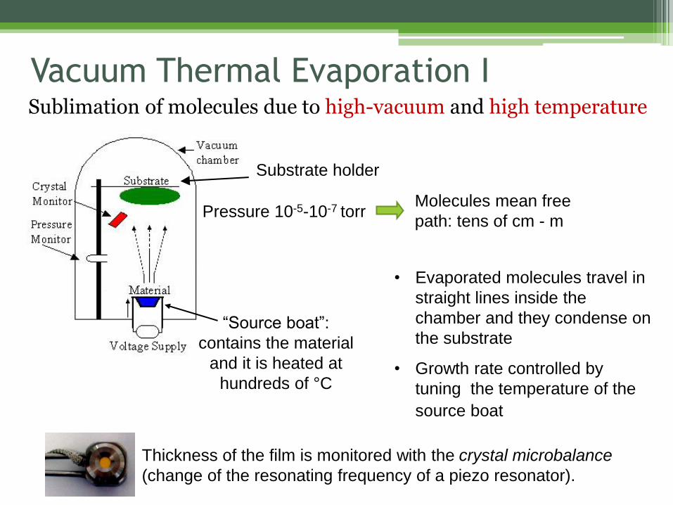
Vacuum Thermal Evaporation I Sublimation of molecules due to high-vacuum and high temperature
Pressure 10-5-10-7 torr Molecules mean free
path: tens of cm - m
“Source boat”:
contains the material
and it is heated at
hundreds of °C
Thickness of the film is monitored with the crystal microbalance
(change of the resonating frequency of a piezo resonator).
Substrate holder
• Evaporated molecules travel in
straight lines inside the
chamber and they condense on
the substrate
• Growth rate controlled by
tuning the temperature of the
source boat
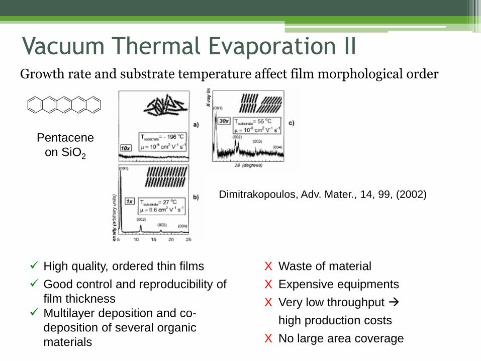
Growth rate and substrate temperature affect film morphological order
High quality, ordered thin films
Good control and reproducibility of
film thickness
Multilayer deposition and co-
deposition of several organic
materials
X Waste of material
X Expensive equipments
X Very low throughput
high production costs
X No large area coverage
Pentacene
on SiO2
Dimitrakopoulos, Adv. Mater., 14, 99, (2002)
Vacuum Thermal Evaporation II
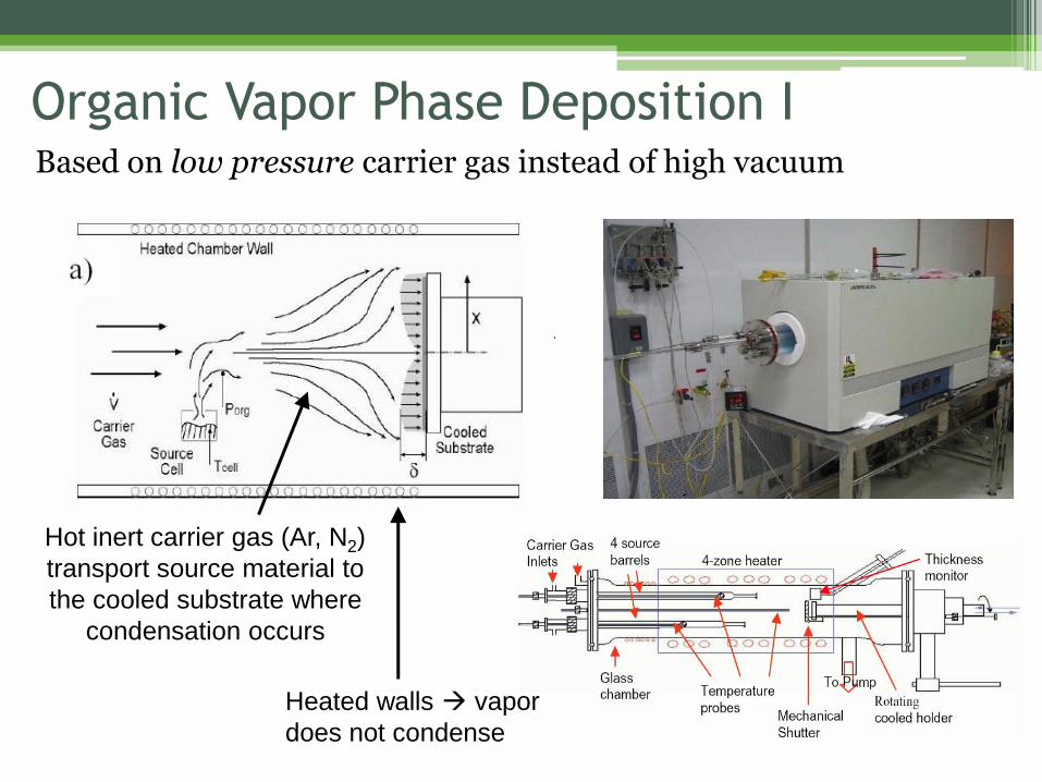
Organic Vapor Phase Deposition I Based on low pressure carrier gas instead of high vacuum
Hot inert carrier gas (Ar, N2)
transport source material to
the cooled substrate where
condensation occurs
Heated walls vapor
does not condense
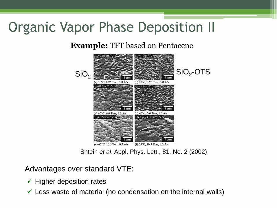
Example: TFT based on Pentacene
Higher deposition rates
Less waste of material (no condensation on the internal walls)
Advantages over standard VTE:
SiO2 SiO2-OTS
Shtein et al. Appl. Phys. Lett., 81, No. 2 (2002)
Organic Vapor Phase Deposition II
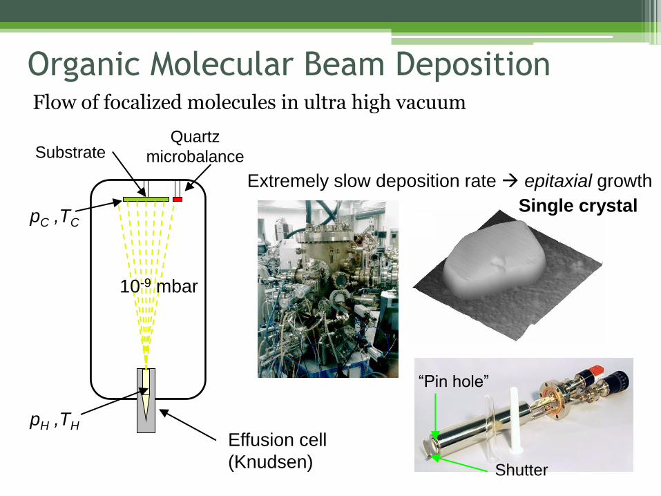
Organic Molecular Beam Deposition Flow of focalized molecules in ultra high vacuum
pC ,TC
Quartz
microbalance
pH ,TH
Substrate
Effusion cell
(Knudsen)
“Pin hole”
Shutter
10-9 mbar
Single crystal
Extremely slow deposition rate epitaxial growth
Baklar et al. Adv. Mater. 2010, 22, 3942–3947
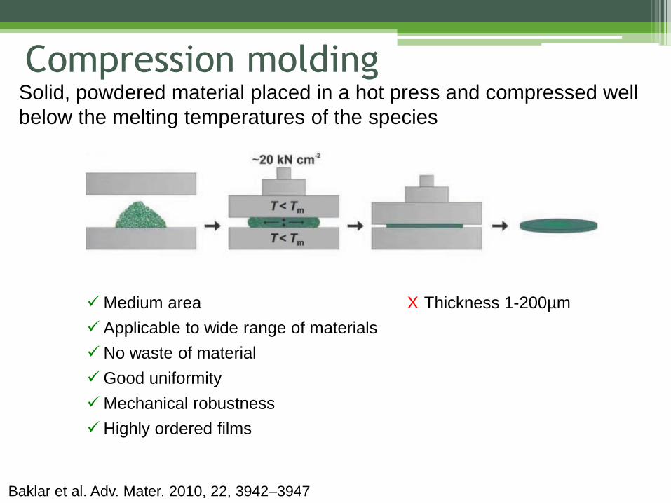
Compression molding Solid, powdered material placed in a hot press and compressed well
below the melting temperatures of the species
Medium area
Applicable to wide range of materials
No waste of material
Good uniformity
Mechanical robustness
Highly ordered films
X Thickness 1-200µm
Compression molding
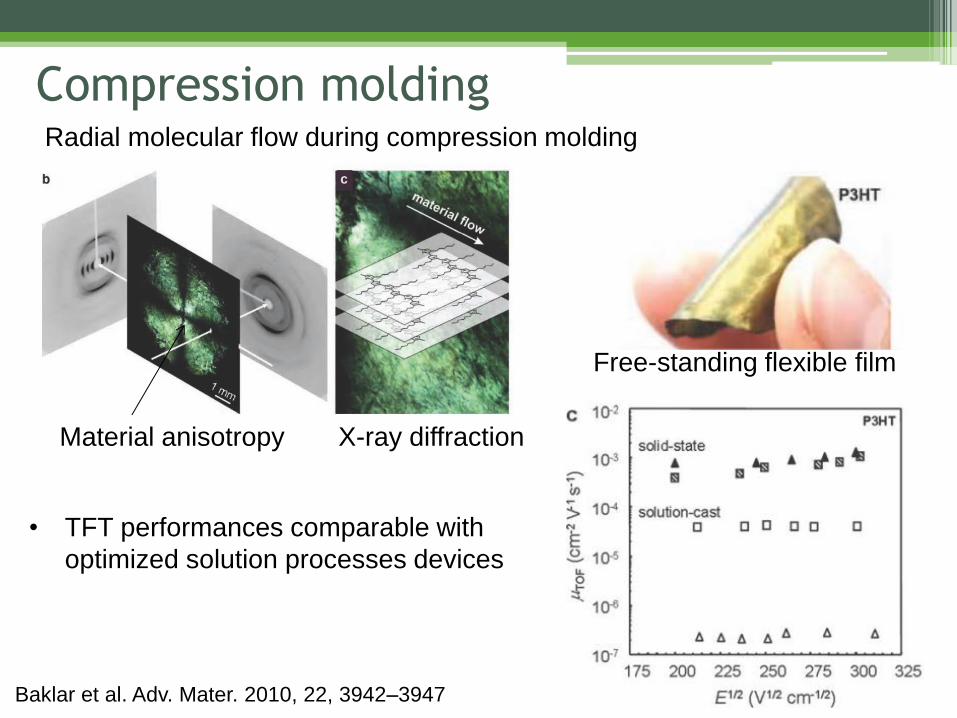
Free-standing flexible film
Radial molecular flow during compression molding
Baklar et al. Adv. Mater. 2010, 22, 3942–3947
Material anisotropy X-ray diffraction
• TFT performances comparable with
optimized solution processes devices
Non-soluble materials:
patterning techniques
• Shadow masking
• Vapor Jet Printing
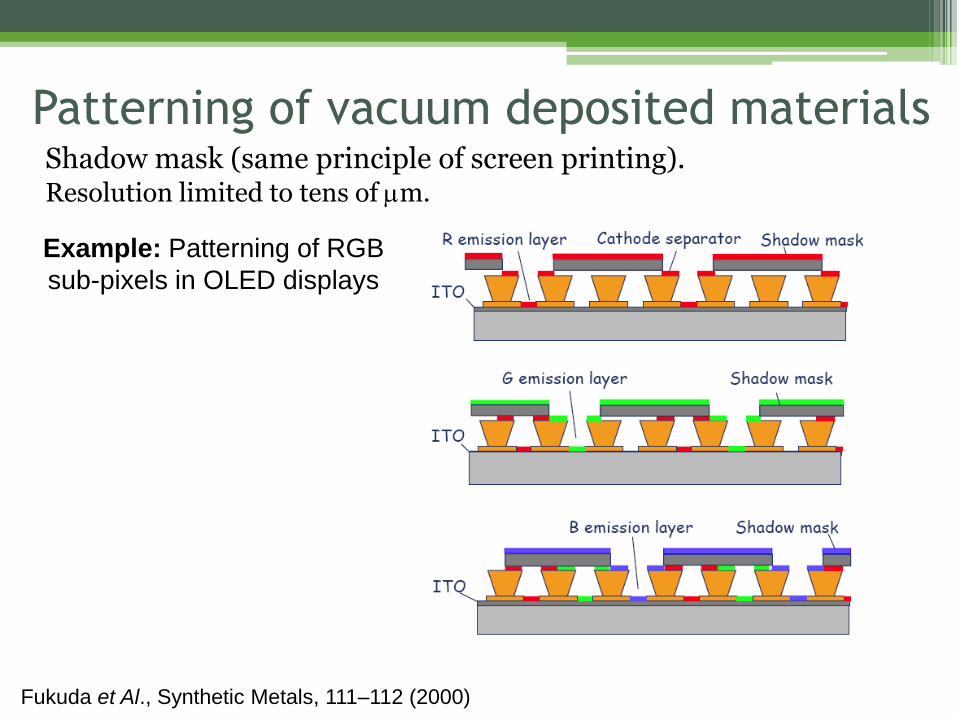
Patterning of vacuum deposited materials Shadow mask (same principle of screen printing). Resolution limited to tens of m.
Example: Patterning of RGB
sub-pixels in OLED displays
Fukuda et Al., Synthetic Metals, 111–112 (2000)
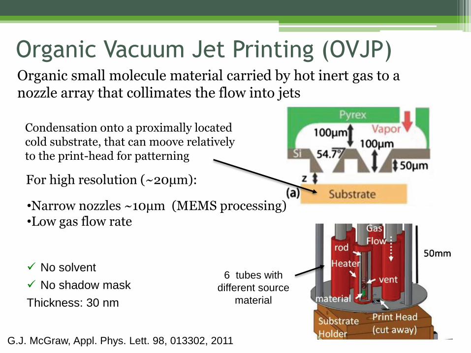
Organic Vacuum Jet Printing (OVJP)
G.J. McGraw, Appl. Phys. Lett. 98, 013302, 2011
Organic small molecule material carried by hot inert gas to a nozzle array that collimates the flow into jets
Condensation onto a proximally located cold substrate, that can moove relatively to the print-head for patterning
•Narrow nozzles ~10μm (MEMS processing) •Low gas flow rate
For high resolution (~20μm):
6 tubes with
different source
material
No solvent
No shadow mask
Thickness: 30 nm