DEPARTMENT WAFER LEVEL SYSTEM INTEGRATION BERLIN · fraunhofer institute for reliability and...
8
FRAUNHOFER INSTITUTE FOR RELIABILITY AND MICROINTEGRATION IZM DEPARTMENT WAFER LEVEL SYSTEM INTEGRATION BERLIN
Transcript of DEPARTMENT WAFER LEVEL SYSTEM INTEGRATION BERLIN · fraunhofer institute for reliability and...
F R A U N H O F E R I N S T I T U T E F O R R E L I A B I L I T Y A N D M I C R O I N T E G R AT I O N I Z M
DEPARTMENT WAFER LEVEL SYSTEM INTEGRATIONBERLIN
WAFER LEVELSYSTEM INTEGRATION
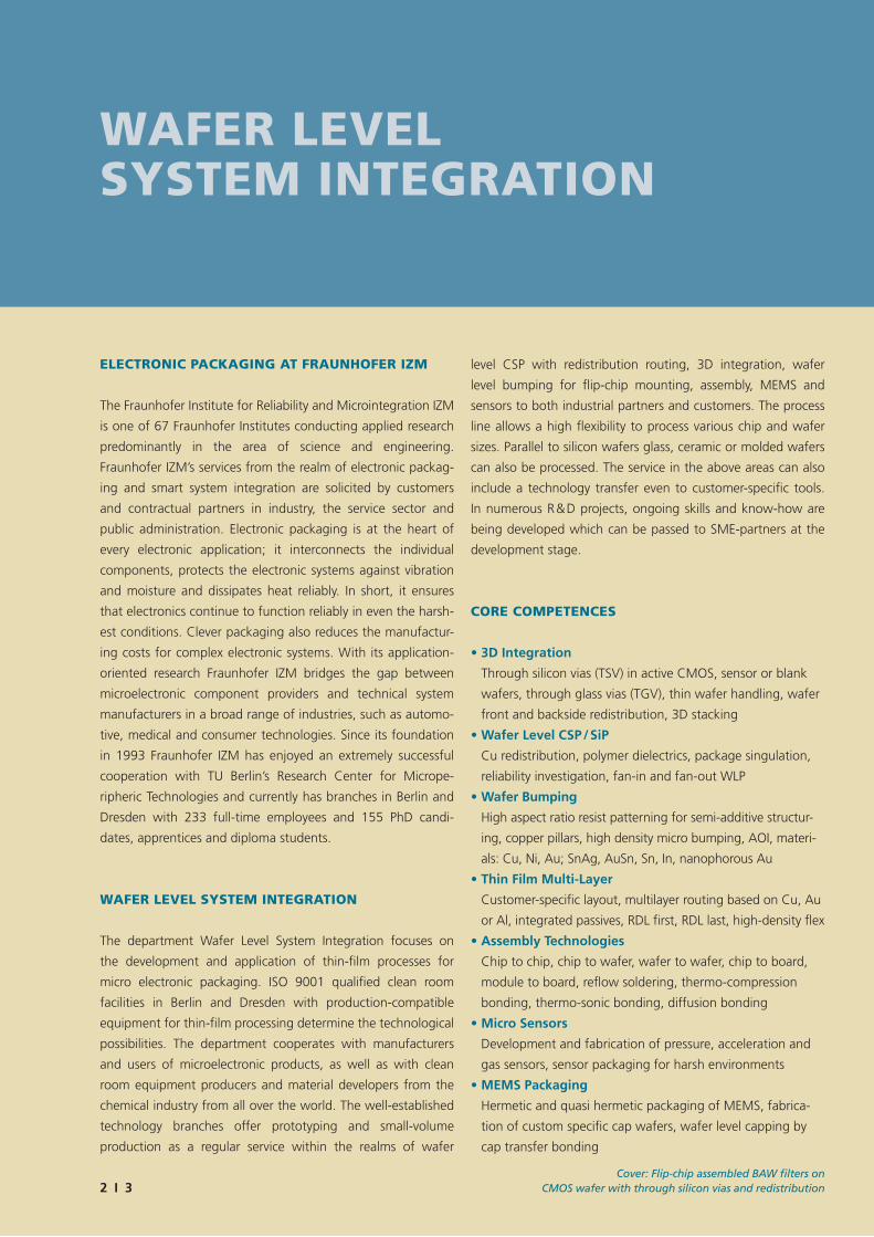
ELECTRONIC PACKAGING AT FRAUNHOFER IZM
The Fraunhofer Institute for Reliability and Microintegration IZM
is one of 67 Fraunhofer Institutes conducting applied research
predominantly in the area of science and engineering.
Fraunhofer IZM’s services from the realm of electronic packag-
ing and smart system integration are solicited by customers
and contractual partners in industry, the service sector and
public administration. Electronic packaging is at the heart of
every electronic application; it interconnects the individual
components, protects the electronic systems against vibration
and moisture and dissipates heat reliably. In short, it ensures
that electronics continue to function reliably in even the harsh-
est conditions. Clever packaging also reduces the manufactur-
ing costs for complex electronic systems. With its application-
oriented research Fraunhofer IZM bridges the gap between
microelectronic component providers and technical system
manufacturers in a broad range of industries, such as automo-
tive, medical and consumer technologies. Since its foundation
in 1993 Fraunhofer IZM has enjoyed an extremely successful
cooperation with TU Berlin’s Research Center for Micrope-
ripheric Technologies and currently has branches in Berlin and
Dresden with 233 full-time employees and 155 PhD candi-
dates, apprentices and diploma students.
WAFER LEVEL SYSTEM INTEGRATION
The department Wafer Level System Integration focuses on
the development and application of thin-film processes for
micro electronic packaging. ISO 9001 qualified clean room
facilities in Berlin and Dresden with production-compatible
equipment for thin-film processing determine the technological
possibilities. The department cooperates with manufacturers
and users of microelectronic products, as well as with clean
room equipment producers and material developers from the
chemical industry from all over the world. The well-established
technology branches offer prototyping and small-volume
production as a regular service within the realms of wafer
2 I 3
level CSP with redistribution routing, 3D integration, wafer
level bumping for flip-chip mounting, assembly, MEMS and
sensors to both industrial partners and customers. The process
line allows a high flexibility to process various chip and wafer
sizes. Parallel to silicon wafers glass, ceramic or molded wafers
can also be processed. The service in the above areas can also
include a technology transfer even to customer-specific tools.
In numerous R & D projects, ongoing skills and know-how are
being developed which can be passed to SME-partners at the
development stage.
CORE COMPETENCES
• 3D Integration
Through silicon vias (TSV) in active CMOS, sensor or blank
wafers, through glass vias (TGV), thin wafer handling, wafer
front and backside redistribution, 3D stacking
• Wafer Level CSP / SiP
Cu redistribution, polymer dielectrics, package singulation,
reliability investigation, fan-in and fan-out WLP
• Wafer Bumping
High aspect ratio resist patterning for semi-additive structur-
ing, copper pillars, high density micro bumping, AOI, materi-
als: Cu, Ni, Au; SnAg, AuSn, Sn, In, nanophorous Au
• Thin Film Multi-Layer
Customer-specific layout, multilayer routing based on Cu, Au
or Al, integrated passives, RDL first, RDL last, high-density flex
• Assembly Technologies
Chip to chip, chip to wafer, wafer to wafer, chip to board,
module to board, reflow soldering, thermo-compression
bonding, thermo-sonic bonding, diffusion bonding
• Micro Sensors
Development and fabrication of pressure, acceleration and
gas sensors, sensor packaging for harsh environments
• MEMS Packaging
Hermetic and quasi hermetic packaging of MEMS, fabrica-
tion of custom specific cap wafers, wafer level capping by
cap transfer bonding
Cover: Flip-chip assembled BAW filters on CMOS wafer with through silicon vias and redistribution
THROUGH VIA INTEGRATION
INTO CMOS, SILICON OR
GLASS WAFERS
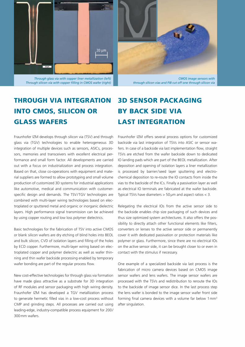
Fraunhofer IZM develops through silicon via (TSV) and through
glass via (TGV) technologies to enable heterogeneous 3D
integration of multiple devices such as sensors, ASICs, proces-
sors, memories and transceivers with excellent electrical per-
formance and small form factor. All developments are carried
out with a focus on industrialization and process integration.
Based on that, close co-operations with equipment and mate-
rial suppliers are formed to allow prototyping and small volume
production of customized 3D systems for industrial applications
like automotive, medical and communication with customer-
specific design and demands. The TSV / TGV technologies are
combined with multi-layer wiring technologies based on elec-
troplated or sputtered metal and organic or inorganic dielectric
layers. High performance signal transmission can be achieved
by using copper routing and low loss polymer dielectrics.
Basic technologies for the fabrication of TSV into active CMOS
or blank silicon wafers are dry etching of blind holes into BEOL
and bulk silicon, CVD of isolation layers and filling of the holes
by ECD copper. Furthermore, multi-layer wiring based on elec-
troplated copper and polymer dielectric as well as wafer thin-
ning and thin wafer backside processing enabled by temporary
wafer bonding are part of the regular process flow.
New cost-effective technologies for through glass via formation
have made glass attractive as a substrate for 3D integration
of RF modules and sensor packaging with high wiring density.
Fraunhofer IZM has developed a TGV metallization process
to generate hermetic filled vias in a low-cost process without
CMP and grinding steps. All processes are carried out using
leading-edge, industry-compatible process equipment for 200 /
300 mm wafers.
3D SENSOR PACKAGING
BY BACK SIDE VIA
LAST INTEGRATION
Fraunhofer IZM offers several process options for customized
backside via last integration of TSVs into ASIC or sensor wa-
fers. In case of a backside via last implementation flow, straight
TSVs are etched from the wafer backside down to dedicated
IO landing pads which are part of the BEOL metallization. After
deposition and opening of isolation layers a liner metallization
is processed by barrier / seed layer sputtering and electro-
chemical deposition to re-route the IO contacts from inside the
vias to the backside of the ICs. Finally a passivation layer as well
as electrical IO terminals are fabricated at the wafer backside.
Typical TSVs have diameters > 50 µm and aspect ratios < 3.
Relegating the electrical IOs from the active sensor side to
the backside enables chip size packaging of such devices and
thus size optimized system architectures. It also offers the pos-
sibility to directly attach other functional elements like filters,
converters or lenses to the active sensor side or permanently
cover it with dedicated passivation or protection materials like
polymer or glass. Furthermore, since there are no electrical IOs
on the active sensor side, it can be brought closer to or even in
contact with the stimulus if necessary.
One example of a specialized backside via last process is the
fabrication of micro camera devices based on CMOS image
sensor wafers and lens wafers. The image sensor wafers are
processed with the TSVs and redistribution to reroute the IOs
to the backside of image sensor dice. In the last process step
the lens wafer is bonded to the image sensor wafer front side
forming final camera devices with a volume far below 1 mm3
after singulation.
CMOS image sensors with through silicon vias and FIB cut off one through silicon via
Through glass via with copper liner metallization (left) Through silicon via with copper filling in CMOS wafer (right)
4 I 5
WAFER LEVEL
REDISTRIBUTION
TECHNOLOGY
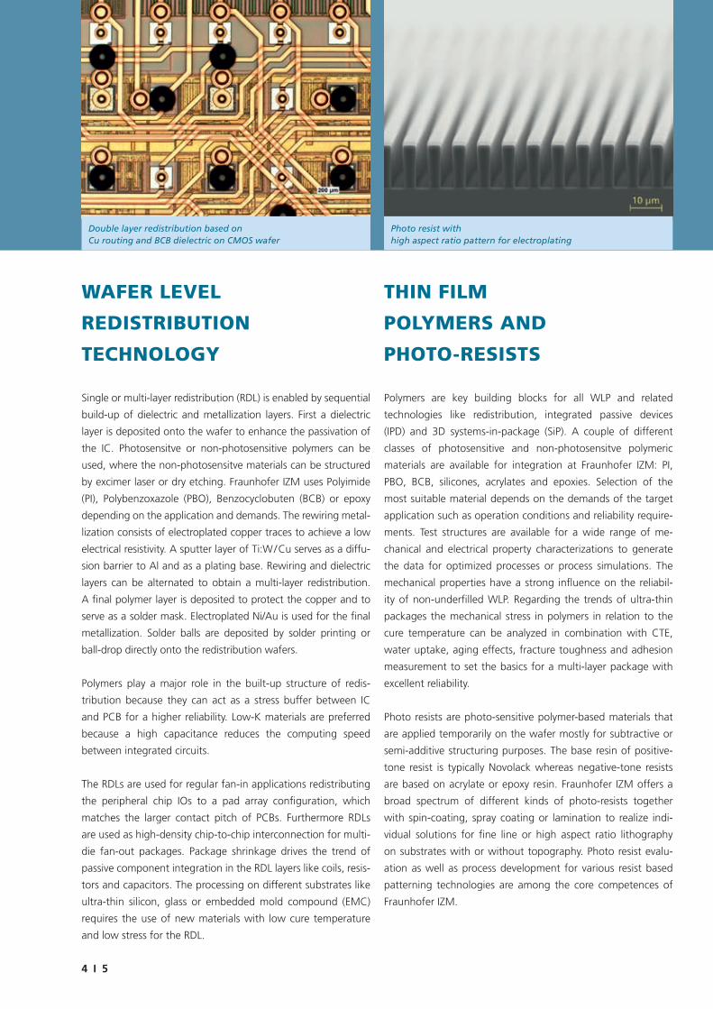
Single or multi-layer redistribution (RDL) is enabled by sequential
build-up of dielectric and metallization layers. First a dielectric
layer is deposited onto the wafer to enhance the passivation of
the IC. Photosensitve or non-photosensitive polymers can be
used, where the non-photosensitve materials can be structured
by excimer laser or dry etching. Fraunhofer IZM uses Polyimide
(PI), Polybenzoxazole (PBO), Benzocyclobuten (BCB) or epoxy
depending on the application and demands. The rewiring metal-
lization consists of electroplated copper traces to achieve a low
electrical resistivity. A sputter layer of Ti:W / Cu serves as a diffu-
sion barrier to Al and as a plating base. Rewiring and dielectric
layers can be alternated to obtain a multi-layer redistribution.
A final polymer layer is deposited to protect the copper and to
serve as a solder mask. Electroplated Ni/Au is used for the final
metallization. Solder balls are deposited by solder printing or
ball-drop directly onto the redistribution wafers.
Polymers play a major role in the built-up structure of redis-
tribution because they can act as a stress buffer between IC
and PCB for a higher reliability. Low-K materials are preferred
because a high capacitance reduces the computing speed
between integrated circuits.
The RDLs are used for regular fan-in applications redistributing
the peripheral chip IOs to a pad array configuration, which
matches the larger contact pitch of PCBs. Furthermore RDLs
are used as high-density chip-to-chip interconnection for multi-
die fan-out packages. Package shrinkage drives the trend of
passive component integration in the RDL layers like coils, resis-
tors and capacitors. The processing on different substrates like
ultra-thin silicon, glass or embedded mold compound (EMC)
requires the use of new materials with low cure temperature
and low stress for the RDL.
THIN FILM
POLYMERS AND
PHOTO-RESISTS
Polymers are key building blocks for all WLP and related
technologies like redistribution, integrated passive devices
(IPD) and 3D systems-in-package (SiP). A couple of different
classes of photosensitive and non-photosensitve polymeric
materials are available for integration at Fraunhofer IZM: PI,
PBO, BCB, silicones, acrylates and epoxies. Selection of the
most suitable material depends on the demands of the target
application such as operation conditions and reliability require-
ments. Test structures are available for a wide range of me-
chanical and electrical property characterizations to generate
the data for optimized processes or process simulations. The
mechanical properties have a strong influence on the reliabil-
ity of non-underfilled WLP. Regarding the trends of ultra-thin
packages the mechanical stress in polymers in relation to the
cure temperature can be analyzed in combination with CTE,
water uptake, aging effects, fracture toughness and adhesion
measurement to set the basics for a multi-layer package with
excellent reliability.
Photo resists are photo-sensitive polymer-based materials that
are applied temporarily on the wafer mostly for subtractive or
semi-additive structuring purposes. The base resin of positive-
tone resist is typically Novolack whereas negative-tone resists
are based on acrylate or epoxy resin. Fraunhofer IZM offers a
broad spectrum of different kinds of photo-resists together
with spin-coating, spray coating or lamination to realize indi-
vidual solutions for fine line or high aspect ratio lithography
on substrates with or without topography. Photo resist evalu-
ation as well as process development for various resist based
patterning technologies are among the core competences of
Fraunhofer IZM.
Double layer redistribution based on Cu routing and BCB dielectric on CMOS wafer
Photo resist with high aspect ratio pattern for electroplating
FAN–OUT
WAFER LEVEL
PACKAGING
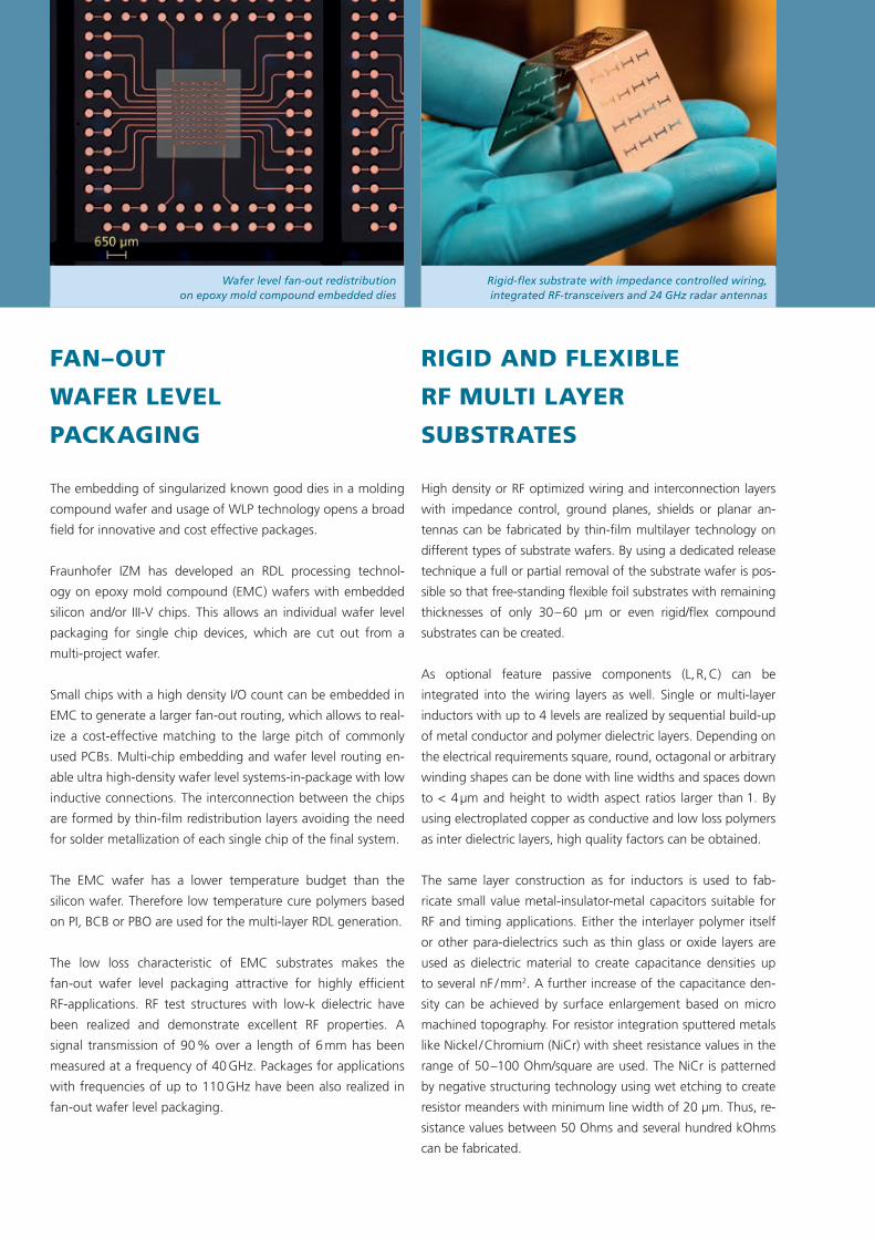
The embedding of singularized known good dies in a molding
compound wafer and usage of WLP technology opens a broad
field for innovative and cost effective packages.
Fraunhofer IZM has developed an RDL processing technol-
ogy on epoxy mold compound (EMC) wafers with embedded
silicon and/or III-V chips. This allows an individual wafer level
packaging for single chip devices, which are cut out from a
multi-project wafer.
Small chips with a high density I/O count can be embedded in
EMC to generate a larger fan-out routing, which allows to real-
ize a cost-effective matching to the large pitch of commonly
used PCBs. Multi-chip embedding and wafer level routing en-
able ultra high-density wafer level systems-in-package with low
inductive connections. The interconnection between the chips
are formed by thin-film redistribution layers avoiding the need
for solder metallization of each single chip of the final system.
The EMC wafer has a lower temperature budget than the
silicon wafer. Therefore low temperature cure polymers based
on PI, BCB or PBO are used for the multi-layer RDL generation.
The low loss characteristic of EMC substrates makes the
fan-out wafer level packaging attractive for highly efficient
RF-applications. RF test structures with low-k dielectric have
been realized and demonstrate excellent RF properties. A
signal transmission of 90 % over a length of 6 mm has been
measured at a frequency of 40 GHz. Packages for applications
with frequencies of up to 110 GHz have been also realized in
fan-out wafer level packaging.
RIGID AND FLEXIBLE
RF MULTI LAYER
SUBSTRATES
High density or RF optimized wiring and interconnection layers
with impedance control, ground planes, shields or planar an-
tennas can be fabricated by thin-film multilayer technology on
different types of substrate wafers. By using a dedicated release
technique a full or partial removal of the substrate wafer is pos-
sible so that free-standing flexible foil substrates with remaining
thicknesses of only 30 – 60 µm or even rigid/flex compound
substrates can be created.
As optional feature passive components (L, R, C) can be
integrated into the wiring layers as well. Single or multi-layer
inductors with up to 4 levels are realized by sequential build-up
of metal conductor and polymer dielectric layers. Depending on
the electrical requirements square, round, octagonal or arbitrary
winding shapes can be done with line widths and spaces down
to < 4 µm and height to width aspect ratios larger than 1. By
using electroplated copper as conductive and low loss polymers
as inter dielectric layers, high quality factors can be obtained.
The same layer construction as for inductors is used to fab-
ricate small value metal-insulator-metal capacitors suitable for
RF and timing applications. Either the interlayer polymer itself
or other para-dielectrics such as thin glass or oxide layers are
used as dielectric material to create capacitance densities up
to several nF / mm2. A further increase of the capacitance den-
sity can be achieved by surface enlargement based on micro
machined topography. For resistor integration sputtered metals
like Nickel / Chromium (NiCr) with sheet resistance values in the
range of 50 –100 Ohm/square are used. The NiCr is patterned
by negative structuring technology using wet etching to create
resistor meanders with minimum line width of 20 µm. Thus, re-
sistance values between 50 Ohms and several hundred kOhms
can be fabricated.
Wafer level fan-out redistribution on epoxy mold compound embedded dies
Rigid-flex substrate with impedance controlled wiring, integrated RF-transceivers and 24 GHz radar antennas
6 I 7
HIGH DENSITY
INTERCONNECTS FOR
FLIP-CHIP ASSEMBLY
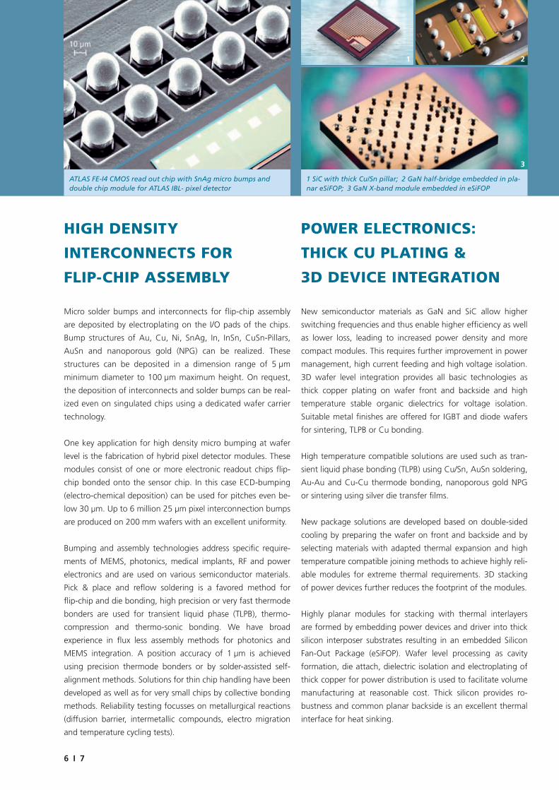
Micro solder bumps and interconnects for flip-chip assembly
are deposited by electroplating on the I/O pads of the chips.
Bump structures of Au, Cu, Ni, SnAg, In, InSn, CuSn-Pillars,
AuSn and nanoporous gold (NPG) can be realized. These
structures can be deposited in a dimension range of 5 µm
minimum diameter to 100 µm maximum height. On request,
the deposition of interconnects and solder bumps can be real-
ized even on singulated chips using a dedicated wafer carrier
technology.
One key application for high density micro bumping at wafer
level is the fabrication of hybrid pixel detector modules. These
modules consist of one or more electronic readout chips flip-
chip bonded onto the sensor chip. In this case ECD-bumping
(electro-chemical deposition) can be used for pitches even be-
low 30 µm. Up to 6 million 25 µm pixel interconnection bumps
are produced on 200 mm wafers with an excellent uniformity.
Bumping and assembly technologies address specific require-
ments of MEMS, photonics, medical implants, RF and power
electronics and are used on various semiconductor materials.
Pick & place and reflow soldering is a favored method for
flip-chip and die bonding, high precision or very fast thermode
bonders are used for transient liquid phase (TLPB), thermo-
compression and thermo-sonic bonding. We have broad
experience in flux less assembly methods for photonics and
MEMS integration. A position accuracy of 1 µm is achieved
using precision thermode bonders or by solder-assisted self-
alignment methods. Solutions for thin chip handling have been
developed as well as for very small chips by collective bonding
methods. Reliability testing focusses on metallurgical reactions
(diffusion barrier, intermetallic compounds, electro migration
and temperature cycling tests).
POWER ELECTRONICS:
THICK CU PLATING &
3D DEVICE INTEGRATION
New semiconductor materials as GaN and SiC allow higher
switching frequencies and thus enable higher efficiency as well
as lower loss, leading to increased power density and more
compact modules. This requires further improvement in power
management, high current feeding and high voltage isolation.
3D wafer level integration provides all basic technologies as
thick copper plating on wafer front and backside and high
temperature stable organic dielectrics for voltage isolation.
Suitable metal finishes are offered for IGBT and diode wafers
for sintering, TLPB or Cu bonding.
High temperature compatible solutions are used such as tran-
sient liquid phase bonding (TLPB) using Cu/Sn, AuSn soldering,
Au-Au and Cu-Cu thermode bonding, nanoporous gold NPG
or sintering using silver die transfer films.
New package solutions are developed based on double-sided
cooling by preparing the wafer on front and backside and by
selecting materials with adapted thermal expansion and high
temperature compatible joining methods to achieve highly reli-
able modules for extreme thermal requirements. 3D stacking
of power devices further reduces the footprint of the modules.
Highly planar modules for stacking with thermal interlayers
are formed by embedding power devices and driver into thick
silicon interposer substrates resulting in an embedded Silicon
Fan-Out Package (eSiFOP). Wafer level processing as cavity
formation, die attach, dielectric isolation and electroplating of
thick copper for power distribution is used to facilitate volume
manufacturing at reasonable cost. Thick silicon provides ro-
bustness and common planar backside is an excellent thermal
interface for heat sinking.
1 SiC with thick Cu/Sn pillar; 2 GaN half-bridge embedded in pla-nar eSiFOP; 3 GaN X-band module embedded in eSiFOP
ATLAS FE-I4 CMOS read out chip with SnAg micro bumps and double chip module for ATLAS IBL- pixel detector
1 2
3
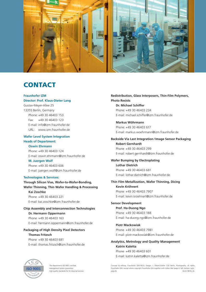
WAFER TO WAFER
BONDING, CAPPING AND
HERMETIC SEALING
Several permanent and temporary wafer to wafer bonding
technologies are available, using fully automated alignment
and bonding equipment. The processes are based on anodic
bonding, direct bonding, thermo-compression bonding, tran-
sient liquid phase bonding, soldering as well as low or room
temperature adhesive bonding. Metallic bonding materials
are deposited by semi-additive, subtractive or lift-off structur-
ing. Adhesive bonding materials are deposited by spin / spray
coating or lamination techniques and structured by photo
patterning, transfer printing, dry etching or laser ablation. Typi-
cal bonding materials include AuSn, CuSn, Au-Au, Cu-Cu as
well as thermally curable or UV curable polymeric adhesives.
Temporary bonding for the handling of wafers with thicknesses
< 50 µm is enabled by adhesive bonding of carrier wafers and
different kinds of de-bonding approaches like thermal slide,
laser exposure or mechanical de-bonding.
Typical application fields of the available bonding techniques
are thin wafer handling, hermetic or quasi-hermetic bonding
of recess wafers for device protection and sealing as well as
functional stacking of active or passive devices like ICs, MEMS,
spacers or lens structures.
The large variety of permanent bonding approaches in combi-
nation with high performance temporary bonding also enables
advanced technologies like wafer level device capping. Such
approaches allow the placement or pre-processing of compo-
nents or custom specific cap / lid structures at temporary carrier
wafers and their subsequent transfer bonding to a target wa-
fer. This approach allows the transferred devices to be laterally
smaller than the landing devices on the target wafer so that
peripheral IOs on the landing devices are still accessible.
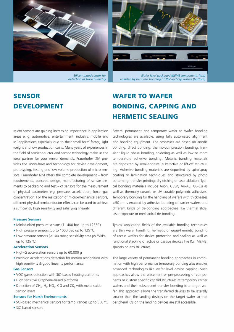
SENSOR
DEVELOPMENT
Micro sensors are gaining increasing importance in application
areas e. g. automotive, entertainment, industry, mobile and
IoT-applications especially due to their small form factor, light
weight and low production costs. Many years of experiences in
the field of semiconductor and sensor technology make us the
ideal partner for your sensor demands. Fraunhofer IZM pro-
vides the know-how and technology for device development,
prototyping, testing and low volume production of micro sen-
sors. Fraunhofer IZM offers the complete development – from
requirements, concept, design, manufacturing of sensor ele-
ments to packaging and test – of sensors for the measurement
of physical parameters e.g. pressure, acceleration, force, gas
concentration. For the realization of micro-mechanical sensors,
different physical semiconductor effects can be used to achieve
a sufficiently high sensitivity and satisfying linearity.
Pressure Sensors
• Miniaturized pressure sensors (1 – 400 bar, up to 125 °C)
• High pressure sensors (up to 1000 bar, up to 125 °C)
• Low pressure sensors (< 100 mbar, sensitivity area μV / VkPa,
up to 125 °C)
Acceleration Sensors
• High-G acceleration sensors up to 60.000 g
• Precision accelerations detection for motion recognition with
high sensitivity & good linearity performance
Gas Sensors
• VOC gases detection with SiC-based heating platforms
• High sensitive Graphene-based platforms
• Detection of CH4, H2, NO2, CO and C02 with metal oxide
sensor layers
Sensors for Harsh Environments
• SOI-based mechanical sensors for temp. ranges up to 350 °C
• SiC-based sensors
Silicon-based sensor for detection of trace humidity
Wafer level packaged MEMS components (top) enabled by hermetic bonding of TSV and cap wafers (bottom)
SERVICE & CONTACT
Combined test stand for swelling of polymers under humidity and heat
Concept & editing: Fraunhofer IZM / WLSI; Design: J. Metze / Atelier f:50 Berlin; Photography: all rights
Fraunhofer IZM, except where copyright Fraunhofer IZM together with Volker Mai (page 6, left, bottom right,
page 8). WLSI 18/09_2e
CONTACTFraunhofer IZM
Director: Prof. Klaus-Dieter Lang
Gustav-Meyer-Allee 25
13355 Berlin, Germany
Phone: +49 30 46403 153
Fax: +49 30 46403 123
E-mail: [email protected]
URL: www.izm.fraunhofer.de
Wafer Level System Integration
Heads of Department:
Oswin Ehrmann
Phone: +49 30 46403 124
E-mail: [email protected]
M. Juergen Wolf
Phone: +49 30 46403 606
E-mail: [email protected]
Technologies & Services:
Through Silicon Vias, Wafer-to-Wafer-Bonding,
Wafer Thinning, Thin Wafer Handling & Processing
Kai Zoschke
Phone +49 30 46403 221
E-mail: [email protected]
Chip Assembly and Interconnection Technologies
Dr. Hermann Oppermann
Phone +49 30 46403 163
E-mail: [email protected]
Packaging of High Density Pixel Detectors
Thomas Fritzsch
Phone +49 30 46403 681
E-mail: [email protected]
Redistribution, Glass Interposers, Thin-Film Polymers,
Photo Resists
Dr. Michael Schiffer
Phone: +49 30 46403 234
E-mail: [email protected]
Markus Wöhrmann
Phone: +49 30 46403 617
E-mail: [email protected]
Backside Via Last Integration / Image Sensor Packaging
Robert Gernhardt
Phone +49 30 46403 299
E-mail: [email protected]
Wafer Bumping by Electroplating
Lothar Dietrich
Phone +49 30 46403 681
E-mail: [email protected]
Thin Film Metallization, Wafer Thinning, Dicing
Kevin Kröhnert
Phone +49 30 46403 7907
E-mail: [email protected]
Sensor Development
Prof. Ha-Duong Ngo
Phone +49 30 46403 188
E-mail: [email protected]
Piotr Mackowiak
Phone +49 30 46403 7981
E-mail: [email protected]
Analytics, Metrology and Quality Management
Katrin Kaletta
Phone +49 30 46403 601
E-mail: [email protected]
The department’s ISO 9001 certified
management system guarantees
high quality standards for its industrial services.