DEPARTMENT OF ELECTRONICS AND …chettinadtech.ac.in/storage/12-06-28/12-06-28-11-57-36-1553... ·...
44
DEPARTMENT OF ELECTRONICS AND COMMUNICATION ENGINEERING COURSE MATERIAL Subject Name : Advanced Microprocessor Class / Sem : BE (ECE) /VII Subject Code : 080290062 Staff Name : Selvan.P Syllabus:: ADVANCED MICROPROCESSORS UNIT I STRUCTURE OF ADVANCED MICROPROCESSORS General Structure of Microprocessors - Microprocessor Architecture –Instruction Set- Data Formats- Instruction Formats – Addressing Modes - - Memory Hierarchy- Register File –Cache- Virtual Memory- Paging- Segmentation- Pipelining- The Instruction Pipeline- Pipeline Hazards- Instruction Parallelism – RISC versus CISC – RISC Properties- RISC Evaluation. UNIT II THE 80386 AND 80486 MICROPROCESSOR 80386 Microprocessors – Special 80386 Registers – 80386 Memory Management –Moving to Protected Mode – Virtual 8086 Mode – The Memory Paging Mechanism – 80486 Microprocessor - 80386 Addressing Modes –Instruction Set.
Transcript of DEPARTMENT OF ELECTRONICS AND …chettinadtech.ac.in/storage/12-06-28/12-06-28-11-57-36-1553... ·...
DEPARTMENT OF ELECTRONICS AND COMMUNICATION ENGINEERING
COURSE MATERIAL
Subject Name : Advanced Microprocessor Class / Sem : BE (ECE) /VII
Subject Code : 080290062
Staff Name : Selvan.P
Syllabus::
ADVANCED MICROPROCESSORS
UNIT I STRUCTURE OF ADVANCED MICROPROCESSORS
General Structure of Microprocessors - Microprocessor Architecture –Instruction
Set- Data Formats- Instruction Formats – Addressing Modes - - Memory
Hierarchy- Register File –Cache- Virtual Memory- Paging- Segmentation-
Pipelining- The Instruction Pipeline- Pipeline Hazards- Instruction Parallelism –
RISC versus CISC – RISC Properties- RISC Evaluation.
UNIT II THE 80386 AND 80486 MICROPROCESSOR
80386 Microprocessors – Special 80386 Registers – 80386 Memory Management
–Moving to Protected Mode – Virtual 8086 Mode – The Memory Paging
Mechanism – 80486 Microprocessor - 80386 Addressing Modes –Instruction Set.
UNIT III THE PENTIUM MICROPROCESSOR
The Software model of the Pentium-Pentium processor registers, Data
organization, instruction types, Addressing modes-Pentium instructions-Interrupt
Processing-Programming the Pentium.
UNIT IV PENTIUM HARDWARE
CPU pin description-RISC concepts-Bus operation-The Pentium’s superscalar
architecture-pipelining-Branch prediction-The instruction and data codes-The
Floating point unit-Protected mode operation-Segmentation Paging Protection
multitasking-Exception-Input/output-Virtual 8086 mode-Pentium II and Beyond.
UNIT V THE MOTOROLA M68000 FAMILY
The MC680X0 Architecture – CPU Registers – Data Formats – Addressing
Modes – Instruction Set and Assembly Directives – Memory Management –
Instruction and Data Cache – Exception Processing.
UNIT .I

UNIT I
STRUCTURE OF ADVANCED MICROPROCESSORS
Contents
1. Describe the function of the microprocessor and detail its basic
operation.
2. Explain the operation of instruction set, data formats, and each
addressing modes.
3. Detail the operation of Memory Hierarchy, Register, Cache, and
Virtual Memory.
4. Detail the operation of paging, segmentation, pipelining
mechanism.
5. Explain the operation of instruction pipeline, pipeline hazardas.
6. Detail the difference between RISC vs CISC.
7. Describe the properties of RISC.
The underlying principles of all computer processors are the same. Fundamentally,
they all take signals in the form of 0s and 1s (thus binary signals), manipulate them
according to a set of instructions, and produce output in the form of 0s and 1s.
The voltage on the line at the time a signal is sent determines whether the signal is
a 0 or a 1. On a 3.3-volt system, an application of 3.3 volts means that it's a 1,
while an application of 0 volts means it's a 0.
Processors work by reacting to an input of 0s and 1s in specific ways and
then returning an output based on the decision. The decision itself happens
in a circuit called a logic gate, each of which requires at least one transistor,
with the inputs and outputs arranged differently by different operations.
The processor's logic gates work together to make decisions using Boolean
logic, which is based on the algebraic system established by
mathematician George Boole.
The main Boolean operators are AND, OR, NOT, and NAND (not AND); In
addition, the processor uses gates in combination to perform arithmetic functions; it can also use them to trigger the storage of data in
memory.
Logic gates operate via hardware known as a switch - in particular,
a digital switch. The most common type of switch in today's
computers is a transistor known as a MOSFET (metal-oxide semiconductor field-effect transistor.
Millions of MOSFETs act together, according to the instructions
from a program, to control the flow of electricity through the logic gates to produce the required result. itself will switch from off to
on, switch from on to off, or stay in its current state.
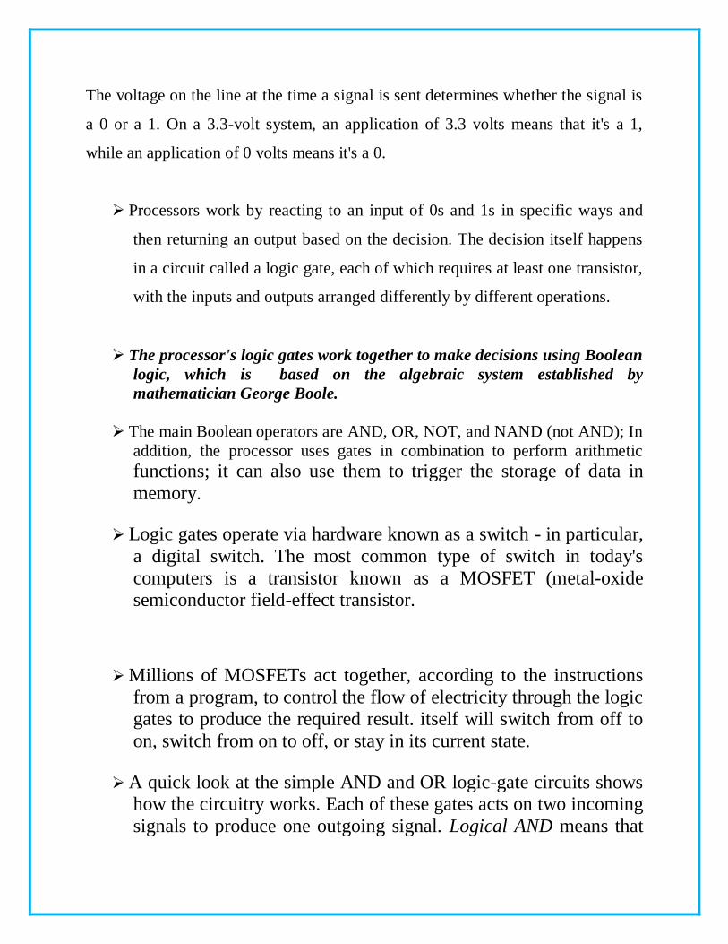
A quick look at the simple AND and OR logic-gate circuits shows how the circuitry works. Each of these gates acts on two incoming
signals to produce one outgoing signal. Logical AND means that
both inputs must be 1 in order for the output to be 1; logical OR
means that either input can be 1 to get a result of 1. In the AND gate, both incoming signals must be high-voltage (or a logical 1)
for the gate.
The flow of electricity through each gate is controlled by that gate's transistor.
However, these transistors aren't individual and discrete units. Instead, large
numbers of them are manufactured from a single piece of silicon (or other
semiconductor material) and linked together without wires or other external
materials. These units are called integrated circuits (ICs), and their development
basically made the complexity of the microprocessor possible. The integration of
circuits didn't stop with the first ICs. Just as the first ICs connected multiple
transistors, multiple ICs became similarly linked, in a process known as large-scale
integration (LSI); eventually such sets of ICs were connected, in a process called
very large-scale integration (VLSI).
Modern day microprocessors contain tens of millions of microscopic
transistors. Used in combination with resistors, capacitors and diodes, these
make up logic gates.
Intel's first claim to fame lay in its high-level integration of all the
processor's logic gates into a single complex processor chip - the Intel 4004 -
released in late 1971.
The 4004 had 46 instructions, using only 2,300 transistors in a 16-pin DIP
and ran at a clock rate of 740kHz (eight clock cycles per CPU cycle of 10.8
microseconds).
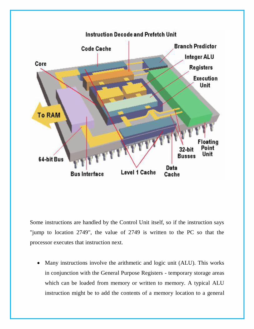
A Pentium processor's major functional components are:
Core: The heart of a Pentium is the execution unit. The Pentium has two
parallel integer pipelines enabling it to read, interpret, execute and despatch
two instructions simultaneously.
Branch Predictor: The branch prediction unit tries to guess which sequence
will be executed each time the program contains a conditional jump, so that
the Prefetch and Decode Unit can get the instructions ready in advance.
Floating Point Unit: The third execution unit in a Pentium, where non-
integer calculations are performed.
Level 1 Cache: The Pentium has two on-chip caches of 8KB each, one for
code and one for data, which are far quicker than the larger external
secondary cache.
Bus Interface: This brings a mixture of code and data into the CPU,
separates the two ready for use, and then recombines them and sends them
back out. All the elements of the processor stay in step by use of a "clock"
which dictates how fast it operates. The very first microprocessor had a
100KHz clock, whereas the Pentium Pro uses a 200MHz clock, which is to
say it "ticks" 200 million times per second.
All the elements of the processor stay in step by use of a "clock" which
dictates how fast it operates.
The very first microprocessor had a 100KHz clock, whereas the Pentium Pro
uses a 200MHz clock, which is to say it "ticks" 200 million times per
second.
Some instructions are handled by the Control Unit itself, so if the instruction says
"jump to location 2749", the value of 2749 is written to the PC so that the
processor executes that instruction next.
Many instructions involve the arithmetic and logic unit (ALU). This works
in conjunction with the General Purpose Registers - temporary storage areas
which can be loaded from memory or written to memory. A typical ALU
instruction might be to add the contents of a memory location to a general
purpose register. The ALU also alters the bits in the Status Register (SR) as
each instruction is executed; this holds information on the result of the
previous instruction.
Typically, the SR has bits to indicate a zero result, an overflow, a carry and
so forth. The control unit uses the information inthe SR to execute
conditional instructions such as "jump to address 7410 if the previous
instruction overflowed". This is about all there is as far as a very basic
processor is concerned and just about any operation can be carried out using
sequences of simple instructions like those described
The 4004 CPU was the forerunner of all of today's Intel offerings and, to date, all
PC processors have been based on the original Intel designs. The first chip used in
an IBM PC was Intel's 8088. This was not, at the time it was chosen, the best
available CPU, in fact Intel's own 8086 was more powerful and had been released
earlier. The 8088 was chosen for reasons of economics: its 8-bit data bus required
less costly motherboards than the 16-bit 8086. Also, at the time that the original PC
was designed, most of the interface chips available were intended for use in 8-bit
designs. These early processors would have nowhere near sufficient power to run
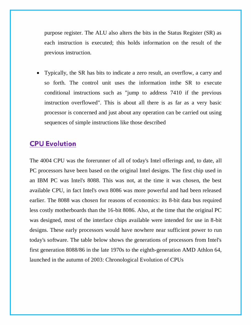
today's software. The table below shows the generations of processors from Intel's
first generation 8088/86 in the late 1970s to the eighth-generation AMD Athlon 64,
launched in the autumn of 2003: Chronological Evolution of CPUs
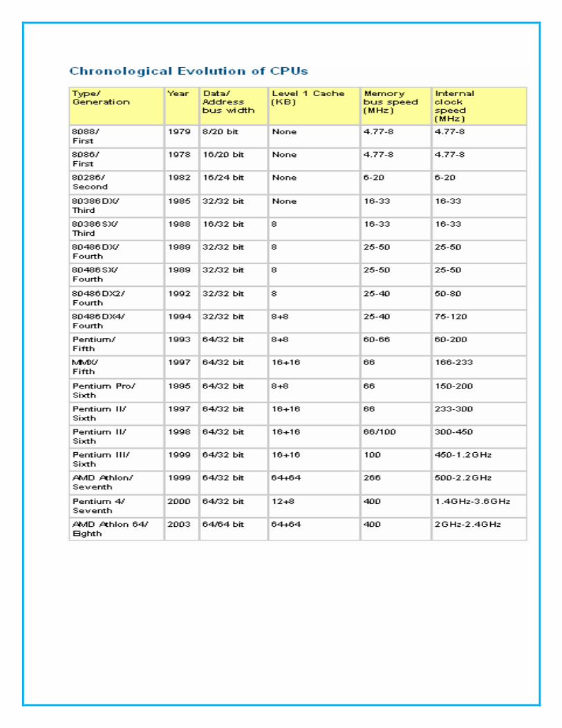
Microprocessor Architecture
Inside the CPU
The basic function of a CPU is to fetch, decode and execute instructions held in
ROM or RAM.
Microprocessors must perform the following activities:
1. Provide temporary storage for addresses and data
2. Perform arithmetic and logic operations
3. Control and schedule all operations
Registers
Registers for a variety of purposes such as holding the address ofinstructions
and data, storing the result of an operation, signaling the result of a logic
operation, or indicating the status of the program or the CPU itself.
Each register has a specific name and is addressable, some, however, are
dedicated to specific tasks while the majority are ‘general purpose’. The
width of a register depends on the type of CPU, e.g., a 16, 32 or 64 bit
microprocessor.
For example, the Pentium processor is a 32 bit CPU, and its registers are 32
bits wide. Some of these are sub-divided and named as 8 and 16 bit registers
in order to run 8 and 16 bit applications designed for earlier x86
microprocessors.
Instruction Register
When the Bus Interface Unit receives an instruction it transfers it to the Instruction
Register for temporary storage. In Pentium processors the Bus Interface Unit
transfers instructions to the L1 I-Cache, there is no instruction register as such.
Stack Pointer
A ‘stack’ is a small area of reserved memory used to store the data in the CPU’s
Registers when:
(1) system calls are made by a process to operating system routines;
(2) When hardware interrupts generated by input/output (I/O) transactions on
Peripheral devices;
(3) when a process initiates an I/O transfer; and
(4) When a process rescheduling event occurs on foot of a hardware timer
Interrupt.
Instruction Decoder
The Instruction Decoder is an arrangement of logic elements which act on the bits
that constitute the instruction
Program or Instruction Counter
The Program Counter (PC) is the register that stores the address in primary
memory (RAM or ROM) of the next instruction to be executed. In 32 bit systems,
this is a 32 bit linear or virtual memory address that references a byte (the first of 4
required to store the 32 bit instruction) in the process’s virtual memory address
space.
Accumulator
The accumulator may contain data to be used in a mathematical or logical
operation, or it may contain the result of an operation. General purpose registers
are used to support the accumulator by holding data to be loaded to/from the
accumulator.
Computer Status Word (CSW) or Flag Register
The result of a ALU operation may have consequences of subsequent operations;
for example, changing the path of execution. Individual bits in the CSW are set or
reset in accordance with the result of mathematical or logical operations. Also
called a flag, each bit in the register has a pre-assigned meaning and the contents
are monitored by the control unit to help control CPU related actions.
Arithmetic and Logic Unit
The Arithmetic and Logic Unit (ALU) performs all arithmetic and logic operations
in a microprocessor viz. addition, subtraction, logical AND, OR, EX-OR, etc. A
typical ALU is connected to the accumulator and general purpose registers and
other CPU components that help transfer the result of its operations to RAM via
the Bus Interface Unit and the system bus. The results may also be written into
internal or external caches.
Control Unit
The control unit coordinates and manages CPU activities, in particular the
execution of instructions by the arithmetic and logic unit (ALU). In Pentium
processors its role is complex, as microcode from decoded instructions are
pipelined for execution by two ALUs.
The System Clock
The Intel 8088 CPU had a clock speed of 4.77 MHz; that is, its internal logic gates
were opened and closed under the control of a square wave pulsed signal that had
a frequency of 4.77 million cycles per second. Alternatively put, the logic gates
opened and closed 4.77 million times per second.
Instruction Cycle
An instruction cycle consists of the activities required to fetch and execute an
instruction. The length of time take to fetch and execute is measured in clock
cycles. In CISC processors this will take many clock cycles, depending on the
complexity of the instruction and number of memory references made to load
operands. In RISC computers the number of clock cycles is reduced significantly.
Addressing Modes
The addressing modes listed below are divided into code addressing and data
Addressing.
The instructions shown below are purely representative in order to illustrate
the addressing modes, and do not necessarily reflect the mnemonics used by
any particular computer.
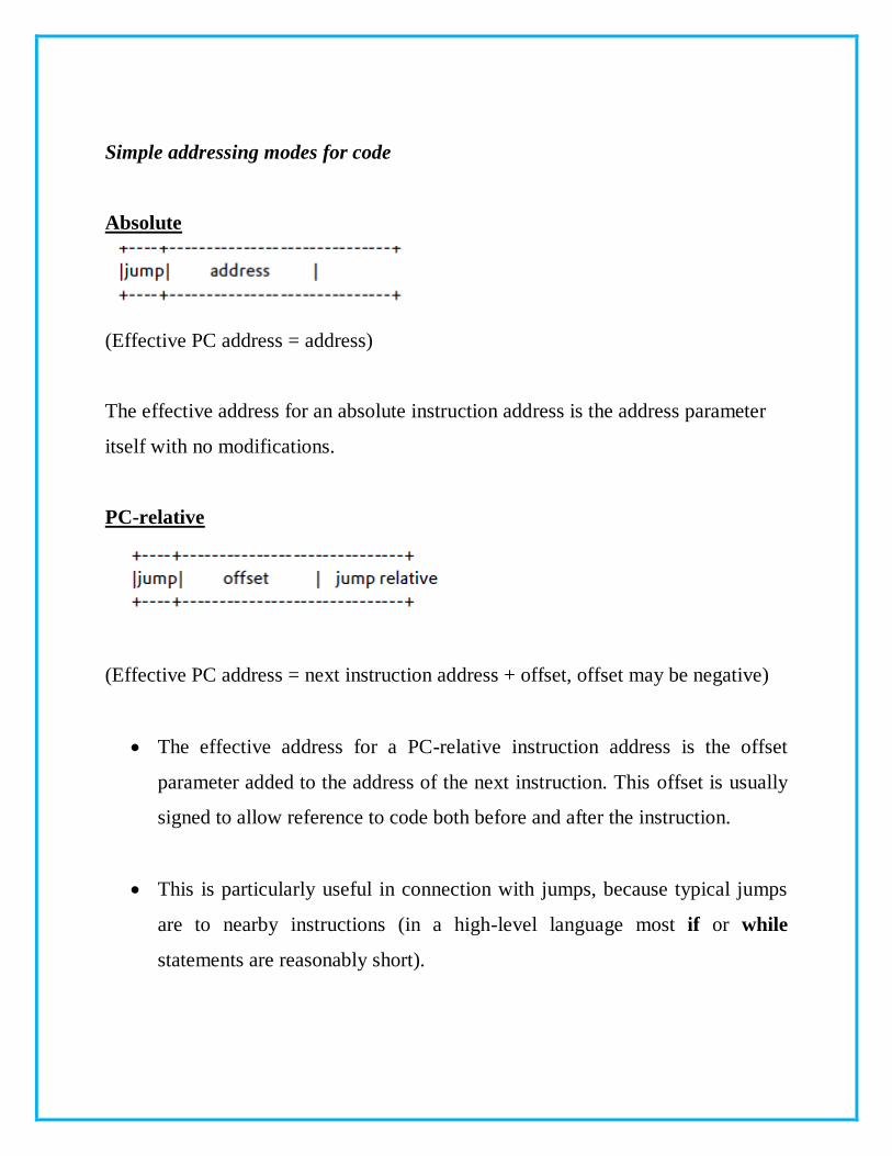
Simple addressing modes for code
Absolute
(Effective PC address = address)
The effective address for an absolute instruction address is the address parameter
itself with no modifications.
PC-relative
(Effective PC address = next instruction address + offset, offset may be negative)
The effective address for a PC-relative instruction address is the offset
parameter added to the address of the next instruction. This offset is usually
signed to allow reference to code both before and after the instruction.
This is particularly useful in connection with jumps, because typical jumps
are to nearby instructions (in a high-level language most if or while
statements are reasonably short).
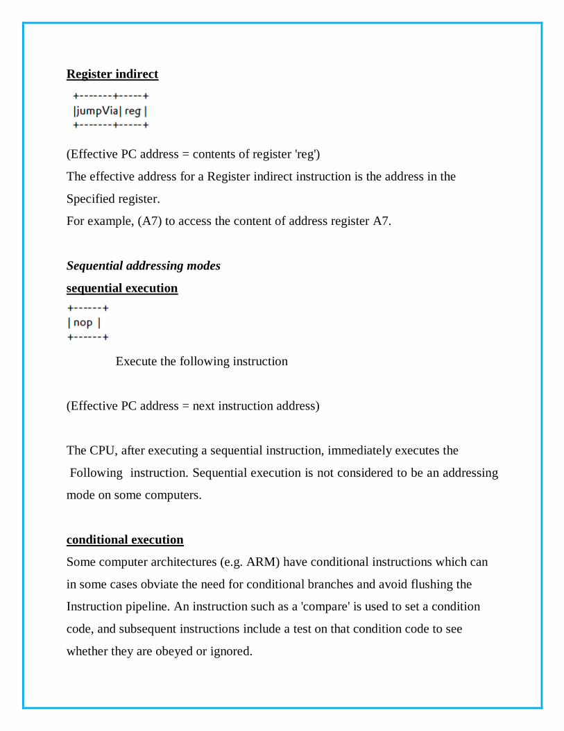
Register indirect
(Effective PC address = contents of register 'reg')
The effective address for a Register indirect instruction is the address in the
Specified register.
For example, (A7) to access the content of address register A7.
Sequential addressing modes
sequential execution
Execute the following instruction
(Effective PC address = next instruction address)
The CPU, after executing a sequential instruction, immediately executes the
Following instruction. Sequential execution is not considered to be an addressing
mode on some computers.
conditional execution
Some computer architectures (e.g. ARM) have conditional instructions which can
in some cases obviate the need for conditional branches and avoid flushing the
Instruction pipeline. An instruction such as a 'compare' is used to set a condition
code, and subsequent instructions include a test on that condition code to see
whether they are obeyed or ignored.
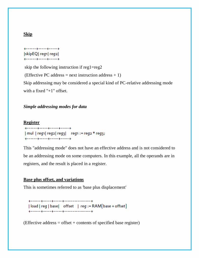
Skip
skip the following instruction if reg1=reg2
(Effective PC address = next instruction address + 1)
Skip addressing may be considered a special kind of PC-relative addressing mode
with a fixed "+1" offset.
Simple addressing modes for data
Register
This "addressing mode" does not have an effective address and is not considered to
be an addressing mode on some computers. In this example, all the operands are in
registers, and the result is placed in a register.
Base plus offset, and variations
This is sometimes referred to as 'base plus displacement'
(Effective address = offset + contents of specified base register)
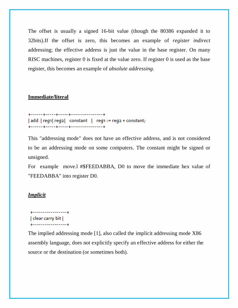
The offset is usually a signed 16-bit value (though the 80386 expanded it to
32bits).If the offset is zero, this becomes an example of register indirect
addressing; the effective address is just the value in the base register. On many
RISC machines, register 0 is fixed at the value zero. If register 0 is used as the base
register, this becomes an example of absolute addressing.
Immediate/literal
This "addressing mode" does not have an effective address, and is not considered
to be an addressing mode on some computers. The constant might be signed or
unsigned.
For example move.l #$FEEDABBA, D0 to move the immediate hex value of
"FEEDABBA" into register D0.
Implicit
The implied addressing mode [1], also called the implicit addressing mode X86
assembly language, does not explicitly specify an effective address for either the
source or the destination (or sometimes both).
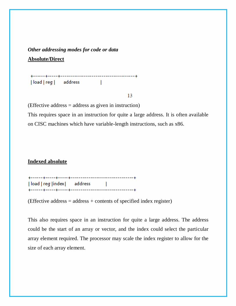
Other addressing modes for code or data
Absolute/Direct
(Effective address = address as given in instruction)
This requires space in an instruction for quite a large address. It is often available
on CISC machines which have variable-length instructions, such as x86.
Indexed absolute
(Effective address = address + contents of specified index register)
This also requires space in an instruction for quite a large address. The address
could be the start of an array or vector, and the index could select the particular
array element required. The processor may scale the index register to allow for the
size of each array element.
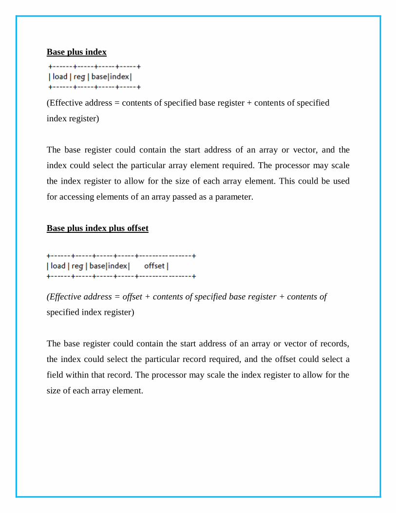
Base plus index
(Effective address = contents of specified base register + contents of specified
index register)
The base register could contain the start address of an array or vector, and the
index could select the particular array element required. The processor may scale
the index register to allow for the size of each array element. This could be used
for accessing elements of an array passed as a parameter.
Base plus index plus offset
(Effective address = offset + contents of specified base register + contents of
specified index register)
The base register could contain the start address of an array or vector of records,
the index could select the particular record required, and the offset could select a
field within that record. The processor may scale the index register to allow for the
size of each array element.
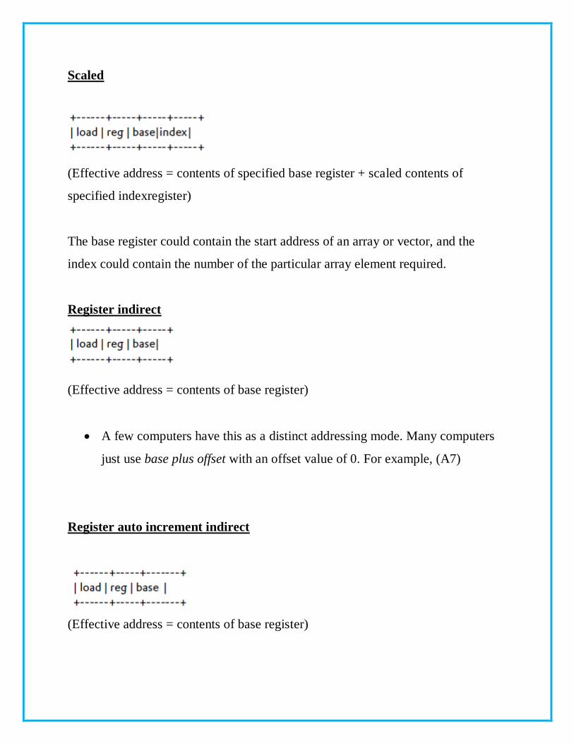
Scaled
(Effective address = contents of specified base register + scaled contents of
specified indexregister)
The base register could contain the start address of an array or vector, and the
index could contain the number of the particular array element required.
Register indirect
(Effective address = contents of base register)
A few computers have this as a distinct addressing mode. Many computers
just use base plus offset with an offset value of 0. For example, (A7)
Register auto increment indirect
(Effective address = contents of base register)
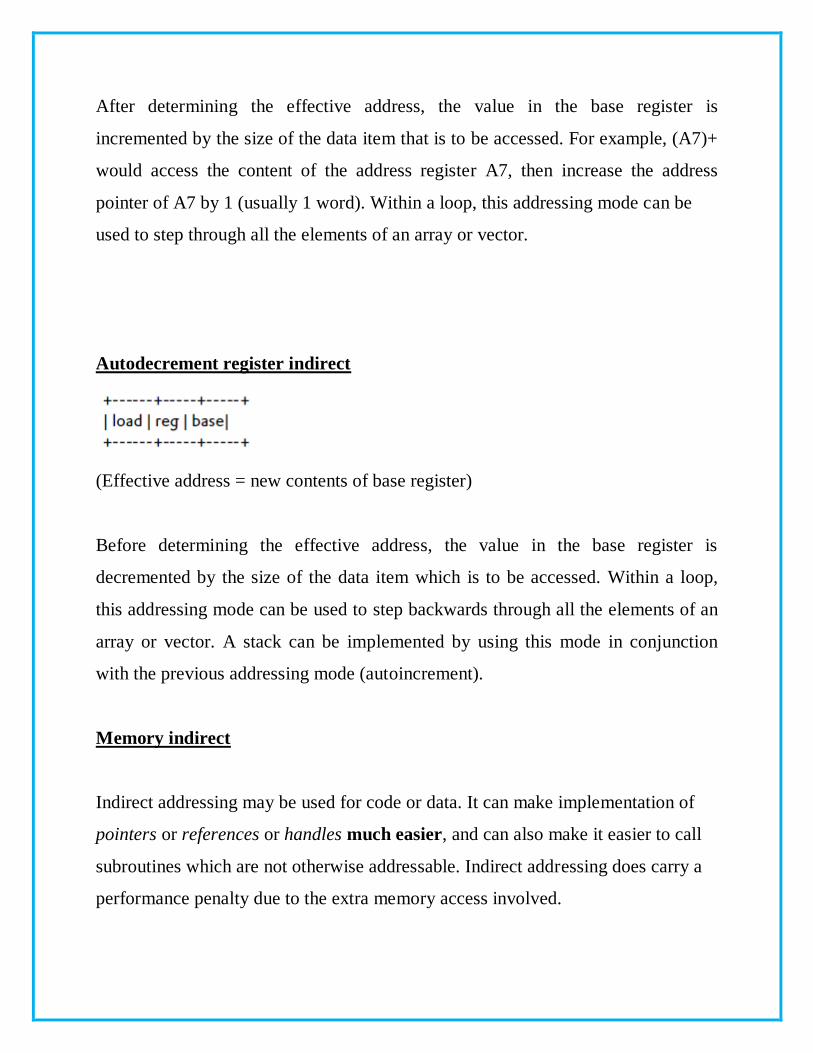
After determining the effective address, the value in the base register is
incremented by the size of the data item that is to be accessed. For example, (A7)+
would access the content of the address register A7, then increase the address
pointer of A7 by 1 (usually 1 word). Within a loop, this addressing mode can be
used to step through all the elements of an array or vector.
Autodecrement register indirect
(Effective address = new contents of base register)
Before determining the effective address, the value in the base register is
decremented by the size of the data item which is to be accessed. Within a loop,
this addressing mode can be used to step backwards through all the elements of an
array or vector. A stack can be implemented by using this mode in conjunction
with the previous addressing mode (autoincrement).
Memory indirect
Indirect addressing may be used for code or data. It can make implementation of
pointers or references or handles much easier, and can also make it easier to call
subroutines which are not otherwise addressable. Indirect addressing does carry a
performance penalty due to the extra memory access involved.
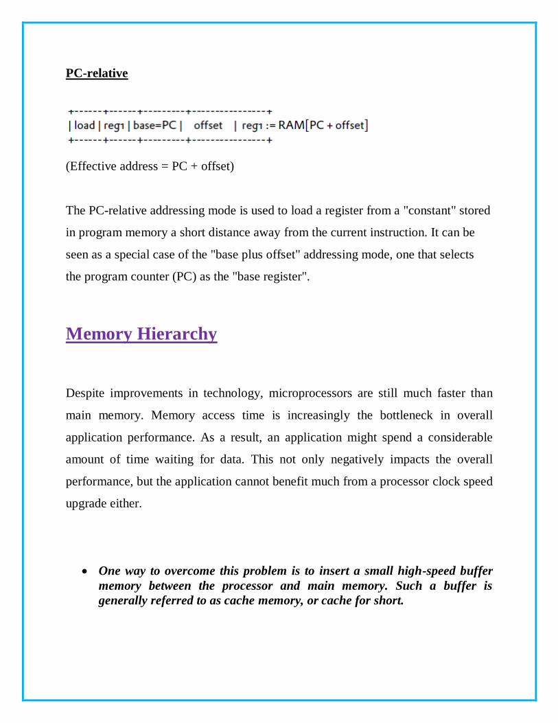
PC-relative
(Effective address = PC + offset)
The PC-relative addressing mode is used to load a register from a "constant" stored
in program memory a short distance away from the current instruction. It can be
seen as a special case of the "base plus offset" addressing mode, one that selects
the program counter (PC) as the "base register".
Memory Hierarchy
Despite improvements in technology, microprocessors are still much faster than
main memory. Memory access time is increasingly the bottleneck in overall
application performance. As a result, an application might spend a considerable
amount of time waiting for data. This not only negatively impacts the overall
performance, but the application cannot benefit much from a processor clock speed
upgrade either.
One way to overcome this problem is to insert a small high-speed buffer
memory between the processor and main memory. Such a buffer is
generally referred to as cache memory, or cache for short.
The application can take advantage of this enhancement by fetching data
from thecache instead of main memory. Of course, there is still traffic
between memory and the cache, but it is
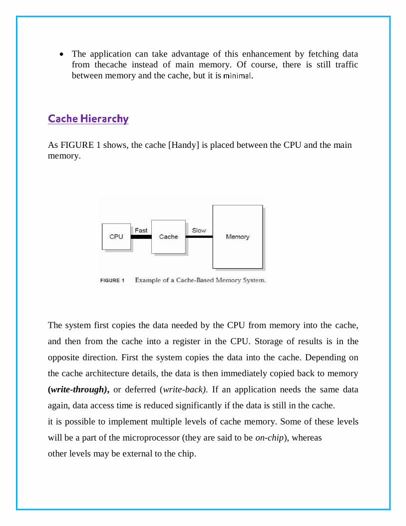
As FIGURE 1 shows, the cache [Handy] is placed between the CPU and the main
memory.
The system first copies the data needed by the CPU from memory into the cache,
and then from the cache into a register in the CPU. Storage of results is in the
opposite direction. First the system copies the data into the cache. Depending on
the cache architecture details, the data is then immediately copied back to memory
(write-through), or deferred (write-back). If an application needs the same data
again, data access time is reduced significantly if the data is still in the cache.
it is possible to implement multiple levels of cache memory. Some of these levels
will be a part of the microprocessor (they are said to be on-chip), whereas
other levels may be external to the chip.
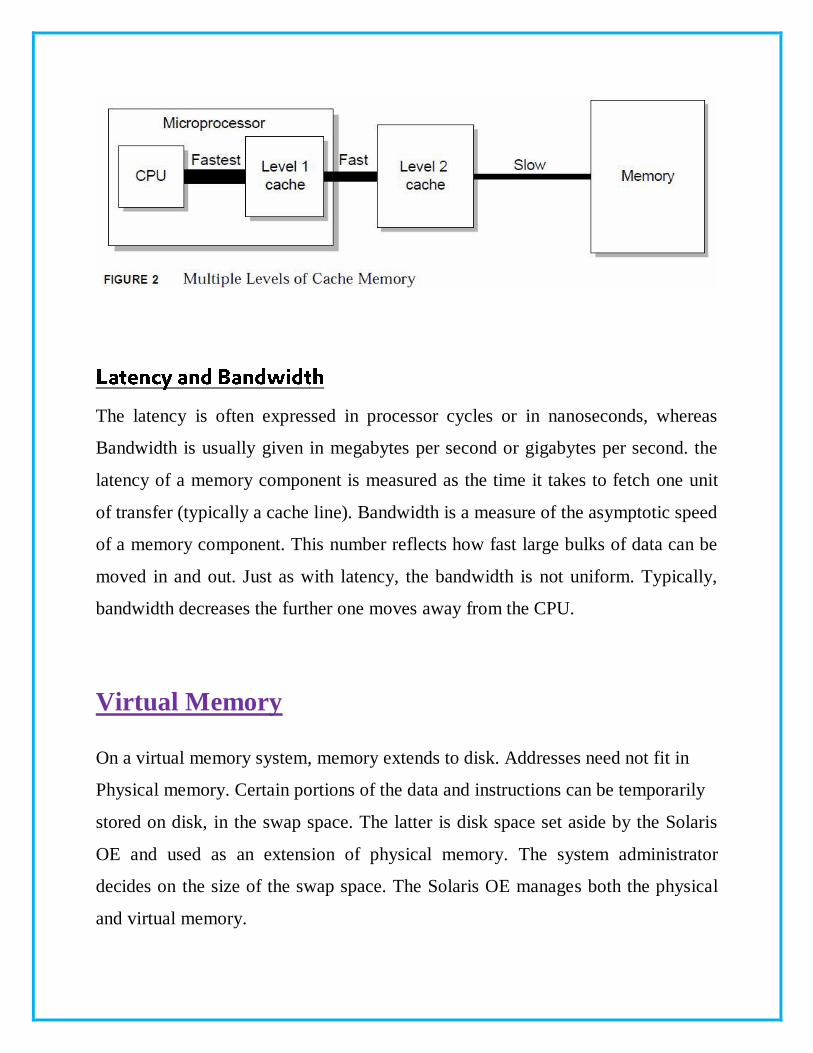
The latency is often expressed in processor cycles or in nanoseconds, whereas
Bandwidth is usually given in megabytes per second or gigabytes per second. the
latency of a memory component is measured as the time it takes to fetch one unit
of transfer (typically a cache line). Bandwidth is a measure of the asymptotic speed
of a memory component. This number reflects how fast large bulks of data can be
moved in and out. Just as with latency, the bandwidth is not uniform. Typically,
bandwidth decreases the further one moves away from the CPU.
Virtual Memory
On a virtual memory system, memory extends to disk. Addresses need not fit in
Physical memory. Certain portions of the data and instructions can be temporarily
stored on disk, in the swap space. The latter is disk space set aside by the Solaris
OE and used as an extension of physical memory. The system administrator
decides on the size of the swap space. The Solaris OE manages both the physical
and virtual memory.
The unit of transfer between virtual memory and physical memory is called
a page.
The size of a page is system dependent.
If the physical memory is completely used up, but another process needs to
run, or a running process needs more data, the Solaris OE frees up space in
memory by moving a page out of the memory to the swap space to make
room for the new page.
The selection of the page that has to move out is controlled by the Solaris
OE.
Various page replacement policies are possible. These replacement policies are,
However, beyond the scope of this article. Certain components in the system (the
CPU for example) use virtual addresses. These addresses must be mapped into the
Physical RAM memory. This mapping between a virtual and physical address is
relatively expensive. Therefore, these translated addresses (plus some other data
structures) are stored in an entry in the so-called Translation Look aside Buffer
(TLB). The TLB is a cache and behaves like a cache. For example, to amortize the
cost of setting up an entry, you would like to reuse it as often as possible. The unit
of virtual management is a page; one entry in the TLB corresponds to one page
pipeline
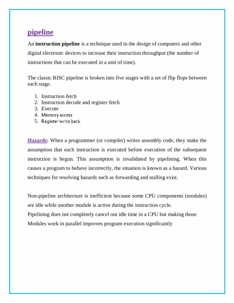
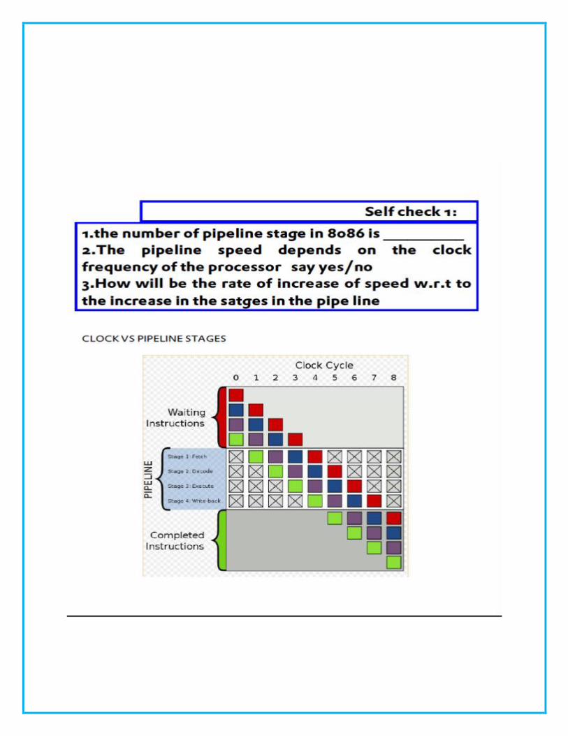
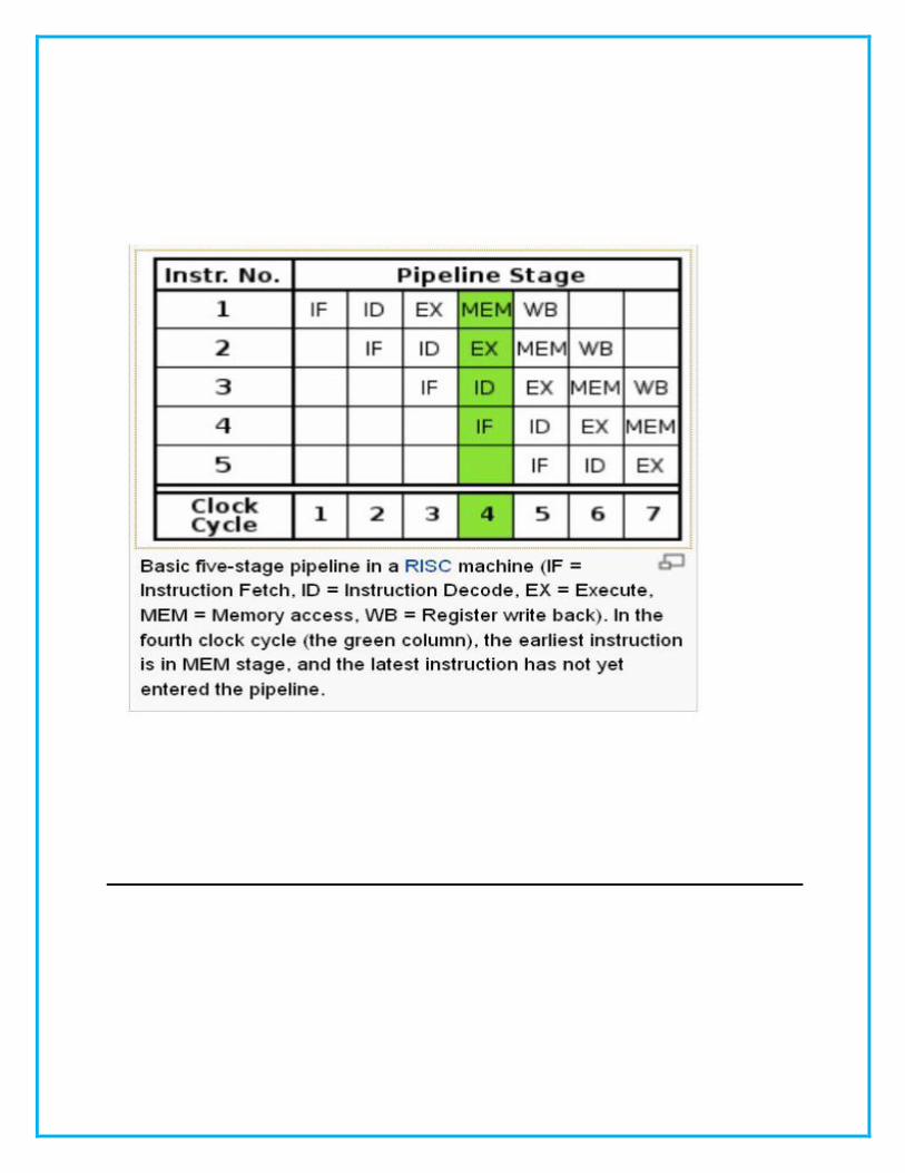
An instruction pipeline is a technique used in the design of computers and other
digital electronic devices to increase their instruction throughput (the number of
instructions that can be executed in a unit of time).
The classic RISC pipeline is broken into five stages with a set of flip flops between
each stage.
1. Instruction fetch
2. Instruction decode and register fetch
3. Execute
4.
5.
Hazards: When a programmer (or compiler) writes assembly code, they make the
assumption that each instruction is executed before execution of the subsequent
instruction is begun. This assumption is invalidated by pipelining. When this
causes a program to behave incorrectly, the situation is known as a hazard. Various
techniques for resolving hazards such as forwarding and stalling exist.
Non-pipeline architecture is inefficient because some CPU components (modules)
are idle while another module is active during the instruction cycle.
Pipelining does not completely cancel out idle time in a CPU but making those
Modules work in parallel improves program execution significantly
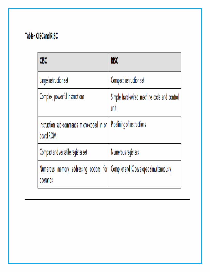
RISC Versus CISC
There are two types of fundamental CPU architecture: complex instruction
set computers (CISC) and reduced instruction set computers (RISC).
CISC is the most prevalent and established microprocessor architecture,
while RISC is a relative newcomer.
Intel’s 80x86 and Pentium microprocessor families are CISC-based,
although RISC-type functionality has been incorporated into Pentium CPUs.
Motorola’s 68000 family of microprocessors is another example of this type
of architecture.
Sun Microsystems’ SPARC microprocessors and MIPS R2000, R3000 and
R4000 families dominate the RISC end of the market; however, Motorola’s
PowerPC, G4, Intel’s i860, and Analog Devices Inc.’s digital signal
processors (DSP) are in wide use.
In the PC/Workstation market, Apple Computers and Sun employ RISC
microprocessors as their choice of CPU.`
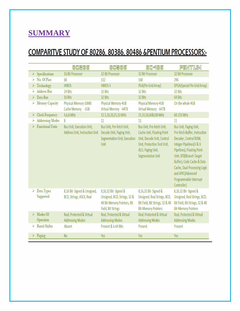
SUMMARY