
Department of Electrical Engineering and Electronicslivrepository.liverpool.ac.uk/3024667/1/Saad...
237
Design of Low Power Electronic Circuits for Bio-Medical Applications Thesis submitted in accordance with the requirements of the University of Liverpool for the degree of Doctor in Philosophy by Saad Ahmed Hasan September 2011 Department of Electrical Engineering and Electronics
Transcript of Department of Electrical Engineering and Electronicslivrepository.liverpool.ac.uk/3024667/1/Saad...

Design of Low Power Electronic Circuits for Bio-Medical
Applications
Thesis submitted in accordance with the requirements of the
University of Liverpool for the degree of Doctor in
Philosophy
by
Saad Ahmed Hasan
September 2011
Department of Electrical Engineering and Electronics

i
ABSTRACT
ABSTRACT
The operational transconductance amplifier, OTA is one of the basic building
blocks in many analogue circuit applications. The low power consumption is an
essential parameter in modern electronic designs for many areas particularly for
portable devices and biomedical applications. For biomedical applications, the low-
power low-voltage OTA-C filters operating at low-frequency ranges are desired. The
low-power, low-voltage operation of electronic devices is very important for
applications such as hearing aids, pacemakers, and EEG. The importance of such
operation is due to the need to implant these electronic circuits inside the body of the
patient for long times before re-charging or replacing the batteries as for pacemakers
and future hearing aids. The small size lightweight wearable EEG systems are
preferable for applications ranging from epilepsy diagnosis to brain-computer
interfaces. The low power consumption is achieved by operation at very small levels of
current. So, in such applications the operation in the nano-ampere current range is
essential to ensure power consumption of nW or few µW. Such very small currents are
obtained through the operation of MOS transistors in their sub-threshold regime. The
design space in such applications is restricted by their specifications which in turn based
on the nature of the application.
In this work, the design and implementation of OTA-C filter topologies for two
bio-medical applications are made and discussed. Those applications are represented by
hearing aids and EEG applications.
In hearing aids, the work focused on cochlear implant and specifically on its
most important stage represented by the filter. Four OTA-C filter topologies are
proposed and two of them are tested experimentally. For the filter in a hearing aid
system, besides its low power operation, it is required to operate with a relatively high
dynamic range of 60dB and above. The dynamic range is the operation space of the

ii
ABSTRACT
filter that specified by the range of signals which can process properly. It is bounded by
the maximum power signal less than its distortion overhead level to the minimum power
signal more than its noise floor. The maximum signal level the filter can perform
properly represents its input linear range. The challenge in CMOS OTA sub-threshold
operation is the very small input linear range which makes it extremely difficult to build
low-power consumed OTA-C filters with a wide dynamic range, DR. In this work, an
OTA with an input linear range of ±900mV for total harmonic distortion, THD<5% is
proposed using MOSFET bumping and capacitor attenuation techniques, combined for
the first time. The minimum signal level the filter can distinguish from noise is still
relatively small with the use of appropriate OTA architecture and using the gm/ID
methodology for MOSFET sizing. So, programmable CMOS OTA-C band-pass filter
topologies operating in sub-threshold region with a dynamic range of 65dB for use in
bionic ears were proposed. The power consumption for the proposed filters is in nano-
Watt range for their frequency range of (100-10k) Hz. Also, a 4-channel OTA-C filter
bank is designed and tested.
The EEG signals have small amplitudes and frequency bands ranges of µV’s and
(1-40) Hz respectively. The important issue is to design filters with small noise floor
with white dominant. This is achieved with the proposed OTA which is of relatively
simple architecture and with operation in the deep weak-inversion region using ±1.5V
supply rails. The OTA-C filter has power consumption in the pico-Watt range for δ, θ,
and α signals and less than 3nW for β signals. Another topology is suggested for future
work.

Dedicated to my parents, aunt & sisters

iii
TABLE OF CONTENTS
TABLE OF CONTENTS
ACKNOWLEDGEMENTS ………………………………………………. x
LIST OF FIGURES ……………………………………………………….. xi
LIST OF TABLES ………………………………………………………… xv
PUBLICATIONS ………………………………………………………….. xviii
LIST OF ABBREVIATIONS …………………………………………….. xix
LIST OF SYMBOLS ………………………………………………………. xxii
CHAPTER ONE Introduction and Review………………………………. 1
1.1 Introduction……………………………………………………………… 1
1.2 Thesis contribution………………………………………………………. 2
1.3 Project Aims……………………………………………………………... 2
1.4 Organization of Thesis ………………………………………………….. 3
1.5 Hearing Aids and OTA-C Filters for their Applications ………………... 4
1.6 The Human Ear………………………………………………………….. 5
1.7 Hearing Deficiencies…………………………………………………….. 7
1.7.1 Conductive impairment…………………………………………...... 7
1.7.2 Sensorineural impairment………………………………………….. 7
1.8 Hearing Loss Categories………………………………………………… 8
1.8.1 Attenuation Loss…………………………………………………… 8

iv
TABLE OF CONTENTS
1.8.2 Compression Loss………………………………………………….. 8
1.8.3 Perceptual Loss…………………………………………………….. 9
1.8.4 Bi-aural Loss (Bilateral hearing loss)……………………………… 9
1.9 Hearing Aids…………………………………………………………….. 9
1.9.1 Conventional Hearing Aids………………………………………… 9
1. Completely-in-the-Canal (CIC)………………………………….. 10
2. In-the-Canal (ITC) ………………………………………………. 10
3. In-the-Ear (ITE)………………………………………………….. 10
4. Behind-the-Ear (BTE)……………………………………………. 10
1.9.2 Bone Anchored Hearing Aids (BAHA)…………………………..... 12
1.9.3 Subcutaneous piezoelectric attached hearing actuator (SPAHA)...... 12
1.9.4 Middle Ear Implants (MEI)………………………………………... 12
1.9.5 Cochlea Implants (CI)……………………………………………… 13
1.9.6 Auditory Brainstem Implants (ABI)……………………………….. 14
1.10 The Coding Strategies of Cochlear Implant……………………………. 14
1.11 Specification of Hearing Aid Design…………………………………... 15
1.12 The use of CMOS OTA-C Filters in Analogue Hearing Aids…………. 15
1.13 Review of Hearing Aid Design Approaches using OTA-C Filters…….. 16
1.14 Conclusion ……………………………………………………………... 19
References…………………………………………………………………… 19
CHAPTER TWO MOSFET in Sub-threshold Regime …………………. 25
2.1 Introduction……………………………………………………………… 25
2.2 MOSFET operation……………………………………………………… 25
2.2.1 Regions of operation……………………………………………….. 25
1. Accumulation…………………………………………………… 27
2. Weak Inversion…………………………………………………. 27

v
TABLE OF CONTENTS
3. Strong Inversion………………………………………………… 28
2.2.2 MOSFET current/voltage Relations……………………………….. 28
1. Strong inversion region……………………………………......... 28
2. Small-signal model of MOSFET ………………………………. 31
3. Weak inversion region………………………………………….. 33
2.3 The Test Chip……………………………………………………………. 39
2.3.1 Introduction………………………………………………………… 39
2.3.2 Architecture………………………………………………………… 40
2.4 Measured and simulated MOSFETs transfer characteristics……………. 41
2.4.1 Transfer Characteristics……………………………………………. 42
2.4.2 Sub-threshold swing ……………………………………………….. 44
2.5 Conclusion……………………………………………………………….. 46
References…………………………………………………………………… 47
CHAPTER THREE OTA LINEARIZATION TECHNIQUES AND
THE PROPOSED OTA ……………………………………………………
49
3.1 Introduction……………………………………………………………… 49
3.2 The simple OTA…………………………………………………………. 49
3.3 Techniques to increase the OTA linear range…………………………… 51
3.3.1 Source Degeneration Technique…………………………………… 52
3.3.2 Bumping MOSFETs Technique…………………………………… 56
3.3.3 Capacitor Attenuation Technique………………………………….. 59
3.4. A Review of Approaches to increase the Linear Range of OTA……….. 61
3.5 The Proposed OTA………………………………………………………. 62
3.6 MOSFET Sizing…………………………………………………………. 64
3.6.1 The gm / ID methodology…………………………………………… 64
3.6.2 The Inversion Coefficient Approach……………………………….. 66

vi
TABLE OF CONTENTS
3.7 Simulation Results……………………………………………………….. 67
3.7.1 OTA MOSFETs sizing utilising gm/ID methodology………………. 67
3.7.2 OTA transfer characteristics and Gm curve………………………… 71
3.8 Experimental Results…………………………………………………….. 76
3.9 Conclusion……………………………………………………………….. 79
References…………………………………………………………………… 80
CHAPTER FOUR Noise In Integrated Circuits ………………………… 84
4.1 Introduction……………………………………………………………… 84
4.2 Types of noise …………………………………………………………... 85
4.2.1 Thermal Noise……………………………………………………... 86
4.2.2 Shot Noise…………………………………………………………. 88
4.2.3 Flicker Noise……………………………………………………..... 89
4.3 Representation of noise in circuits……………………………………… 91
4.4 Another strategy of noise representation………………………………... 92
4.5 Noise for MOSFET and OTA…………………………………………… 93
4.5.1 Noise in MOSFET…………………………………………………. 93
4.5.2 Noise in the simple OTA Circuit depending on strategy of 4.3…… 94
4.5.3 Noise in the sub-threshold simple OTA depending on strategy of
4.4…………………………………………………………………..
97
4.5.4 Noise in Cascaded Amplifiers…………………………………….. 101
4.5.5 Noise in a system consisting of a feedback loop…………………... 102
4.5.6 Noise in the Proposed OTA………………………………………. 104
4.6 Conclusion……………………………………………………………….. 106
References…………………………………………………………………… 107

vii
TABLE OF CONTENTS
CHAPTER FIVE The Proposed OTA-C Filters for Cochlear Implants.. 109
5.1 Introduction……………………………………………………………… 109
5.2 Proposed Filter Topologies……………………………………………… 109
5.2.1 Topology 1………………………………………………………..... 109
1. Transfer function derivation…………………………………… 110
2. Finding the Filter poles………………………………………… 113
5.2.2 Topology 2…………………………………………………………. 114
1. Transfer function derivation……………………………………. 115
2. Finding the filter poles………………………………………….. 116
5.2.3 Topology 3 ……………………………………………………........ 117
1. Transfer function derivation……………………………………. 118
2. Finding the filter poles………………………………………….. 120
5.2.4 Topology 4……………………………………………………........ 120
1. Transfer function derivation…………………………………… 121
2. Finding the filter poles ………………………………………... 124
5.3 Design Details…………………………………………………………... 125
5.3.1 Specifications…………………………………………………… 125
5.3.2 MOSFET Sizing………………………………………………… 125
5.4 Simulation Results……………………………………………………… 127
5.4.1 The Frequency Response….……………………………….............. 127
1. Topologies 1 and 2…………………………………………….. 127
2. Topologies 3 and 4…………………………………………….. 129
5.4.2 Noise ………………………………………………………………. 131
1. Simulation……………………………………………………… 131
2. Noise calculations……………………………………………… 135
I. Noise of Topology 1………………………………………. 136
II. Noise of Topology 2……………………………………… 137

viii
TABLE OF CONTENTS
III. Noise of Topology 3………………………………………. 138
IV. Noise of Topology 4………………………………………. 138
5.4.3 The Filter Dynamic Range………………………………………… 139
5.4.4 Realisation of the Proposed Filter Topologies 3 and 4 ……………. 141
5.5 Experimental Work……………………………………………………... 142
5.5.1 Frequency Response……………………………………………….. 142
5.5.2 Noise……………………………………………………………..... 144
5.6 Input linear range increase effect on dynamic range…………………… 147
5.6.1 Linear range and frequency bandwidth of filter topologies 147
5.6.2 Dynamic range and the noise power……………………………….. 149
5.6.3 Dynamic range and the filter frequency bandwidth 150
5.7 The 4-Channel Filter Bank……………………………………………... 150
5.7.1 The Frequency Response………………………………………… 152
5.8 Figure of Merit………………………………………………………….. 153
5.9 Conclusion……………………………………………………………… 156
References…………………………………………………………………… 156
CHAPTER SIX PROPOSED OTA-C FILTER FOR EEG……............... 160
6.1 Introduction……........................................................................................ 160
6.2 Design Details…………………………………………………………… 160
6.2.1 Specifications………………………………………………………. 160
6.2.2 MOSFET Sizing……………………………………………………. 161
6.2.3 The operation of MOSFETs in deep weak inversion region………. 166
1. Mismatch and bandwidth………………………………………. 167
2. Noise …………………………………………………………… 167
6.3 The OTA-C band-pass filters for EEG…………………………………... 168
6.3.1 Design approaches………………………………………………... 168

ix
TABLE OF CONTENTS
6.3.2 The OTA-C filter in this work……………………………………. 169
1. Transfer function derivation……………………………………. 170
2. Finding filter poles ……………………………………………... 172
6.4 Simulation Results……………………………………………………… 173
6.4.1 The Frequency Response………………………………………….. 173
6.4.2 Noise……………………………………………………………… 176
6.5 Experimental Work……………………………………………………... 178
6.5.1 The Frequency Response………………………………………..... 178
6.5.2 Noise……………………………………………………………... 179
6.6 Figure of Merit for the OTA-C Filter…………………………………... 182
6.7 Conclusion……………………………………………………………… 184
References…………………………………………………………………… 185
CHAPTER SEVEN CONCLUSIONS AND FURTHER WORK ……… 187
7.1 Conclusions……………………………………………………………… 187
7.1.1 Cochlear Implants………………………………………………….. 187
7.1.2 EEG Signals……………………………………………………....... 191
7.2 Further Work…………………………………………………………… 193
APPENDICIES …………………………………………………………….. 196
Appendix A Derivation of average power for correlated noise sources ……. 196
Appendix B Detailed derivations of transfer functions of the proposed
Topologies……………………………………………………………………
197
B.1 Derivation of the transfer function of Topology 1 ……………………... 197
B.2 Derivation of the transfer function of Topology 2 ……………………... 199
B.3 Derivation of the transfer function of Topology 3 ……………………... 200

x
TABLE OF CONTENTS
B.4 Derivation of the transfer function of Topology 4 ……………………... 202
B.5 Obtaining the poles of the proposed Topology 4 ………………………. 206

xi
ACKNOWLEDGMENTS
ACKNOWLEDGMENTS
Alhamdulillah, I hope to be able to thank almighty ALLAH for giving me the
capability to say Alhamdulillah for everything.
My sincere gratitude to my Supervisor professor S. Hall for providing me with
all support I needed in all years of my study. He always encourages me and gives me
the important advices and notes related with all stages of my work. I’d like to thank my
2nd
supervisor Dr. J. Marsland for his time, guidance and support. Also, my gratitude to
my colleague Dr. Thomas Dowrick for his great help especially, in the 1st year of my
study. Also I’d like to acknowledge the Iraqi ministry of Higher education and scientific
research for sponsoring my study and undertaking the fabrication cost of the test chip
with the department of Electrical Engineering and Electronics in the University of
Liverpool which also contributes the technical support.

xii
LIST OF FIGURES
LIST OF FIGURES
Figure 1.1 Human Ear taken from [2.1]
5
Figure 1.2 Conventional hearing aids technologies
11
Figure 1.3 Block diagram of a bionic ear consisting of M-channels signal
processor
13
Figure 2.1 NMOSFET, (a) Symbol. (b) Cross sectional view
26
Figure 2.2 Ideal MOSFET small-signal model
31
Figure 2.3 MOSFET small-signal model after adding channel modulation
effect
33
Figure 2.4 Inversion layer charge density versus distance from source to
drain in the MOSFET weak inversion operation mode
35
Figure 2.5 MOSFET small-signal model
37
Figure 2.6 2.6mm×2.6mmm Fabricated test chip
39
Figure 2.7 Measured and simulated transfer characteristic for MOSFETs
with W=6µm, L=6µm and at VDS=0.1V
42
Figure 2.8 Measured and simulated transfer characteristic for MOSFETs
with W=30µm, L=6µm and at VDS=0.1V
43
Figure 3.1 Simple OTA
50
Figure 3.2 Source degradation linearization techniques for simple
differential OTA; (a) Single resistor diffuser, (b) single
MOSFET diffuser, (c) double MOSFETs diffusers, (d) diode
connected MOSFETs
53
Figure 3.3 Simple OTA with bumping MOSFETs technique of
linearisation
57
Figure 3.4 Simple OTA with capacitor attenuation technique
60

xiii
LIST OF FIGURES
Figure 3.5 Proposed OTA
63
Figure 3.6 Obtaining the gm/ID versus ID/(W/L) curve; (a) NMOSFET
transfer characteristics, (b) gm/ID versus VGS curve for
NMOSFET, (c) PMOSFET transfer characteristics, (d) gm/ID
versus VGS curve for PMOSFET, (e) The obtained the gm/ID
versus ID/(W/L) curves for NMOS and PMOS transistors
68
Figure 3.7 Normalised currents distribution in the simple OTA
Figure 3.8 Normalised currents distribution in OTA with bumping
MOSFETs with aspect ratio of bumping MOSFETs double
that of input MOSFETs
71
72
Figure 3.9 Transfer characteristics of simple, bumped, and the proposed
OTAs
73
Figure 3.10 Normalised transconductance versus differential input voltage
curves for the simple, bumped, and the proposed OTAs
indicating their input linear range
74
Figure 3.11 Simulated and measured input linear range of the proposed
OTA
77
Figure 3.12 The Measured percentage variation in the input linear range
of the proposed OTA
78
Figure 4.1 Thermal noise representation of the MOSFET, (a) Thermal
noise current source (b) Thermal noise voltage source
87
Figure 4.2 Concept of flicker noise corner frequency
Figure 4.3 Representation of noise by voltage and current sources
90
92
Figure 4.4 Noise model of the simple OTA, (a) Taking the equivalent
sources for each MOSFET (b) The overall equivalent noise
model for the simple OTA
95
Figure 4.5 Small signal noise circuit of the simple OTA 98
Figure 4.6 Noise performance of a cascade of amplifiers,(a) A cascade of
noisy amplifiers with their corresponding input-referred noise
sources (b) The equivalent noise model for (a)
102

xiv
LIST OF FIGURES
Figure 4.7 Block diagram of a system with a feedback loop
103
Figure 4.8 Block diagram of a system with a feedback loop and various
noise sources
104
Figure 5.1 Proposed OTA-C filter topology1
110
Figure 5.2 Proposed OTA-C filter topology2
114
Figure 5.3 Proposed OTA-C filter topology3
118
Figure 5.4 Proposed OTA-C filter topology4
121
Figure 5.5 Simulated frequency response of the Topology 1 OTA
128
Figure 5.6 Simulated frequency response of the Topology 2 OTA
129
Figure 5.7 Simulated frequency response of the Topology 3 OTA
130
Figure 5.8 Simulated frequency response of the Topology 4 OTA
130
Figure 5.9 Simulated output noise of the Topology 1 OTA-C band-pass
filter for the (100-200) Hz and (5-10) kHz frequency bands
132
Figure 5.10 Simulated output noise of the Topology 2 OTA-C band-pass
filter for the (100-200) Hz and (5-10) kHz frequency bands
133
Figure 5.11 Simulated output noise of the Topology 3 OTA-C band-pass
filter for the (100-200) Hz and (5-10) kHz frequency bands
134
Figure 5.12 Simulated output noise of the Topology 4 OTA-C band-pass
filter for the (100-200) Hz and (5-10) kHz frequency bands
135
Figure 5.13 Simulated and measured frequency response of the proposed
(Topology 1) OTA-C band-pass filter
143
Figure 5.14 Simulated and measured frequency response of the proposed
(Topology 2) OTA-C band-pass filter
144
Figure 5.15 Measured and simulated output noise of the Topology 1
OTA-C band-pass filter for the (100-200) Hz and (5-10) kHz
frequency bands
145

xv
LIST OF FIGURES
Figure 5.16 Measured and simulated output noise of the Topology 2
OTA-C band-pass filter for the (100-200) Hz and (5-10) kHz
frequency bands
146
Figure 5.17 Block Diagram of the 4-Channel OTA-C Filter Bank
Consisting of 4- Individual Parallel Stages of Topology
1filters
151
Figure 5.18 Measured frequency response for the 4-channel OTA-C filter
bank
152
Figure 6.1 Measured and simulated transfer characteristic for MOSFETs
with W=12µm, L=12µm and at VDS=0.1V
162
Figure 6.2 Proposed OTA for EEG applications 164
Figure 6.3 Proposed OTA frequency response showing the transition
frequency, fT at 10pA bias current
166
Figure 6.4 OTA-C band-pass filter for EEG applications
170
Figure 6.5 Block diagram of the proposed OTA-C filter for EEG
applications
172
Figure 6.6 Simulated frequency response of the OTA-C filter for EEG
signals
174
Figure 6.7 Simulated frequency response of the OTA-C filter for EEG
signals for nominal (straight lines) and deviation (dashed
lines) cases
175
Figure 6.8 Simulated noise of the OTA-C band-pass filter for EEG signals
178
Figure 6.9 Measured frequency response of the OTA-C filter for EEG
signals
179
Figure 6.10 Measured noise of the OTA-C band-pass filter for EEG
signals
180

xvi
LIST OF TABLES
LIST OF TABLES
Table 2.1: Key device parameters for BSIM3v3.1 model in
AMS process for 0.35µm CMOS C35 Technology
41
Table 2.2: S values for figures 2.7 and 2.8 with the error
45
Table 2.3: κ values for figures 2.7 and 2.8 figures with the error
45
Table 2.4: Threshold voltage values for figures 2.7 and 2.8 with
the error
46
Table 3.1: The dimensions of MOSFETs of the proposed OTA
70
Table 3.2: The simulated IB and fT ranges of the proposed OTA
74
Table 3.3: A comparison of OTA input linear range using
different linearisation techniques
75
Table 3.4: The measured IB and fT ranges of the proposed OTA
78
Table 4.1: Noise contribution and the noise transfer functions
due to noise current sources in the simple OTA
99
Table 5.1: The dimensions of OTA MOSFETs of the proposed
topologies1 and 2
126
Table 5.2: The dimensions of OTA MOSFETs of the proposed
topologies3 and 4
126
Table 5.3: The important simulation results related to the OTA-
C band-pass filter topologies 1, 2, 3, and 4 at (100-
200) Hz frequency band
140
Table 5.4: The Important simulation results related to the OTA-
C band-pass filter topologies 1, 2, 3, and 4 at (5-10)
kHz frequency band
140
Table 5.5: The important measured results related to the OTA-C
band-pass filter topologies 1 and 2 at (100-200) Hz
frequency band
146

xvii
LIST OF TABLES
Table 5.6: The important measured results related to the OTA-C
band-pass filter topologies 1 and 2 at (5-10) kHz
frequency band
147
Table 5.7: The figure of merit for the four proposed filter
topologies in this work
154
Table 5.8: Comparison with other weak inversion topologies
presented in literature (only those with experimental
results are considered except topologies 3 and 4 in
this work with their simulation results)
154
Table 6.1: The sub-threshold swing and threshold voltage for
figures 6.1 with the error
163
Table 6.2: The dimensions of MOSFETs of the proposed OTA
164
Table 6.3: The important simulated results related to the OTA-C
band pass filter
175
Table 6.4: The 1/f noise corner frequency values for EEG bands
181
Table 6.5: The important measured results related to the OTA-C
band-pass filter
181
Table 6.6: The figure of merit for the measured EEG frequency
bands
182
Table 6.7: Comparison with other weak inversion topologies
presented in literature
183

xviii
PUBLICATIONS
PUBLICATIONS
1. S. A. Hasan, S. Hall, and J. S. Marsland, “A Proposed Sub-Threshold OTA-C for
Hearing Aids,” Proceeding of 9th IEEE International NEWCAS Conference, pp.
414-417, June 2011, Bordeaux, France.
2. S. A. Hasan, S. Hall, and J. S. Marsland, “A Wide Linear Range OTA-C Filter for
Bionic Ears,” 3rd Computer Science and Electronic Engineering Conference,
CEEC’11, UK, pp.19-22, July, 2011, Essex, UK. (The best paper award).

xix
LIST OF ABBREVIATIONS
LIST OF ABBREVIATIONS
ABI
Auditory Brainstem Implants
AGC
Automatic Gain Control
ADC
Analogue to digital converter
AER
Address-Event Representation
AMS
Austria micro systems
B
Bulk of MOSFET
BAHA
Bone Anchored Hearing Aids
BCI
Brain-Computer Interface
BTE
Behind-the-Ear
CIC
Completely-in-the-Canal
CIs
Cochlear Implants
CLBTs
Compatible Lateral Bipolar Transistors
C-level
Comfortable level
xx
LIST OF ABBREVIATIONS
CMOS Complementary Metal Oxide Semiconductor
D
Drain of MOSFET
DSP Digital Signal Processing
EEG
Electroencephalography
EKV
MOSFET model made by C. Enz, F. Krummenacher and E. Vitloz.
FD SOI
Fully depleted silicon on insulator wafer technology
FOM
Figure of merit
G
Gate of MOSFET
HA Hearing Aid
ITC
In-the-Canal
ITE
In-the-Ear
KCL
Kirchhoff’s current law
M
Number of cascaded stages
MEI
Middle Ear Implants
MOSFET Metal Oxide Semiconductor Field Effect Transistor

xxi
LIST OF ABBREVIATIONS
OTA-C
Operational Transconductance Amplifier- Capacitor
PFM
Pulse-Frequency Modulated
S
Source of MOSFET
SNR
Signal to Noise Ratio
SPAHA
Subcutaneous Piezoelectric Attached Hearing Actuator
T-level Threshold level of
UV
Ultra violet
VLSI
Very Large Scale Integration
a(s)
Feed forward stage in a system
e(s)
Error signal in a system
f(s)
Feedback stage in a system
H(s)
Transfer function of the OTA-C filter

xxii
ABSTRACT
LIST OF SYMBOLS
a
Capacitive attenuation ratio
a-1
Number of times of increase of the input linear range due to capacitive
attenuation technique
Av
Open loop voltage gain
Cdep, Depletion region capacitance
Cgb
Gate -bulk capacitance
Cgd
Gate -drain capacitance
Cgs,
Gate -source capacitance
CIs
Cochlear Implants
CL
Total capacitance at the OTA output node “load capacitance”
COX Gate -oxide capacitance
DR
Dynamic range
E Electric field
f0
Centre frequency
fc
Flicker noise corner frequency
fH
High frequency
fl Low frequency
fT
OTA transition frequency
Gm
OTA transconductance
gm MOSFET transconductance

xxiii
ABSTRACT
gmb
MOSFET bulk transconductance
gs Summation of MOSFET’s transconductance and bulk transconductance
gsd
MOSFET source-drain conductance
IB
OTA bias current
IC
Inversion coefficient
ID MOSFET drain current
IG
MOSFET gate current
IN
Normalised current
Iout
MOSFET output current
k
Boltzmann constant
K
Process and transistor dependent parameter
KF
Flicker noise coefficient
KFn
Flicker noise coefficient in n-channel MOSFET
KFp
Flicker noise coefficient in p-channel MOSFET
Kp
Polynomial pole coefficient in filter transfer function
Kz
Polynomial zero coefficient in filter transfer function
L
MOSFET effective length
L’
MOSFET effective length with channel length modulation
M
Number of cascaded stages
m
Ratio of the single diffussor aspect ratio to that of the input MOSFET

xxiv
ABSTRACT
MB Bumping MOSFET
MSD
Source degradation MOSFET
n
MOSFET body effect coefficient “slope factor”
N
Number of shot-noise sources
n+
High impurity n-type silicon
ne
Effective body effect coefficient
p
Pole in filter transfer function
Q
Quality factor
q
Electron charge
Q’I
Charge density of inversion layer in the weak inversion region
QB
Depletion region charge density
QFG
Floating gate residual charge
QI
Charge density of inversion layer in the strong inversion region
R
Resistor
r
Capacitor ratio in a capacitive attenuator
rO
MOSFET output resistor due to channel length modulation effect
S Sub-threshold swing
St
Ratio of bump MOSFETs aspect ratio to that of input MOSFETs
T
Absolute temperature
THD
Total harmonic distortion
u
Velocity

xxv
ABSTRACT
UT
Thermal voltage
VB
OTA bias voltage
VD
Drain voltage
Vd
OTA differential input voltage
VDS
Gate-drain voltage
VG
Gate voltage
VGB
Gate-bulk voltage
VGS
Gate-source voltage
Vin
Input voltage
Vin1
OTA non-inverting input terminal
Vin2
OTA inverting input terminal
VL
OTA Input linear range
Vout Output voltage
VPP
Peak to peak voltage
Vrms
Volt root- mean-square- value
VS
Source voltage
VTH
Threshold voltage
W
MOSFET effective width
Δf
Frequency bandwidth
κ
Sub-threshold electrostatic coupling coefficient of the MOSFET gate
and channel

xxvi
ABSTRACT
кe Effective sub-threshold electrostatic coupling coefficient between the
MOSFET gate and channel
Thermalni___
2
Thermal noise current
shotni___
2
Shot noise current
RMSnv ,
MOSFET RMS value of noise voltage
RMSeqnv ,, OTA RMS value of noise voltage
fnv/
___
1
2
Flicker noise power
Thermalnv___
2
Thermal noise power
innv___
,
2
OTA input-referred noise power
RMSoutnv,
___2
RMSeqinnv,,
___2
RMS value of output noise power
RMS value of total input-referred noise power for a system consisting
of many stages ___
2
nv
MOSFET total noise power
Factor affected by the MOSFET operation regime which equals to ½
and 2/3 for sub-threshold and above threshold respectively
λ
Channel length modulation parameter
µn
Average mobility of electrons
µO
Low-field mobility
µp
Average mobility of holes
ψs Surface potential

1
CHAPTER ONE Introduction and Review
LOW POWER ELECTRONIC CIRCUITS FOR BIOMEDICAL APPLICATIONS Saad A. Hasan
CHAPTER ONE
Introduction and Review
1.1 Introduction
Analogue integrated OTA-C filters are the most important building stages in
wearable and implantable medical devices such as cochlear implants, CI and
Electroencephalography, EEG systems. Such devices are used for many purposes such
as diagnosing medical problems, restoring lost body functions, and brain–computer
interface (BCI) systems [1.1]. Due to the nature of physiological signals and the
corresponding application scenarios, the filters designed for such low frequency
applications should meet stringent specifications. The most important specifications are
represented by efficient power consumption, low voltage operation, low input-referred
noise, high performance and flexibility.
The objective of designing circuits with low power consumption in the range of
micro watts is to increase the battery life-time. This means that the systems can operate
for a long time in terms of years instead of days or weeks before the need to recharge or
replace their batteries. The low voltage operation allows the use of small size batteries
which is reflected in a decrease of the entire size of the system. Also, many other
specifications like price should be taken in account, hence, the choice of whether to use
analogue or digital configurations for the filter and the other stages of such systems.
Furthermore the choice of DSP strategies for the entire system depends on the trade-offs
in satisfying the required specifications. Therefore, adopting hybrid mixed-signal
implementation should give the best compromise for these applications. Therefore, a

2
CHAPTER ONE Introduction and Review
LOW POWER ELECTRONIC CIRCUITS FOR BIOMEDICAL APPLICATIONS Saad A. Hasan
system consisting of analogue and digital parts is feasible since in CMOS technology this
can be accomplished on the same chip.
A filter has a dynamic range of operation limited by two constraints. The first one
is the upper limit above which the output is distorted. This limit is represented by the
filter input linear range. The lower limit is the input-referred noise floor. In this work,
both limits of the dynamic range of the proposed filters are discussed in detail. Besides,
the upper limit is increased, especially for the filters which are proposed for hearing aids
application. This work provides the trade-offs in satisfying the specifications for
cochlear implants and EEG applications.
1.2 Thesis Contribution
In this work, an OTA with a large input linear range of ±900 mV is presented. This
is accomplished by combining MOSFET bumping and capacitor attenuation techniques
together, for the first time. In this approach, the proposed OTA has a simple structure
and relatively low noise. The proposed OTA is used to construct four, 2nd
order OTA-C
band-pass filter topologies suitable for hearing aids applications. Two of those filters are
tested experimentally. A parallel 4-channel OTA-C filter bank for hearing aids
applications is also proposed and experimentally tested. Finally, a 4th
order OTA-C
band-pass filter suitable for EEG applications is proposed, built, and tested
experimentally.
1.3 Project Aim
The target of this research is to develop low power electronic circuits that can be
used as a frequency extraction stage in modern biomedical applications such as hearing
aids and EEG systems. Hearing aids are used to overcome hearing deficiencies that

3
CHAPTER ONE Introduction and Review
LOW POWER ELECTRONIC CIRCUITS FOR BIOMEDICAL APPLICATIONS Saad A. Hasan
arise from simple problems related to outer or middle ear to severe problems due to
damage in the inner ear.
Electroencephalography is a tool to record signals that represent the brain
electrical activity which are measured by electrodes placed on the scalp. The EEG
signals lie within four different frequency bands namely δ, θ, α, and β, characterised by
their low voltage amplitudes and frequency. Those signals reflect different human
activities and are very important in clinical tests for diagnosis ranging from epileptic fits
to brain death and other brain disorders. Recently EEG signals are also used in
computer- brain interface systems, CBI which represents a direct communication
pathway between the brain and an external device [1.2]. This application is aimed to
augment, assist or repair human cognitive or sensory-motor functions. An example of
this is the enabling of signals from the brain to control some external activity to help a
person suffering from paralysis to write a book, control a prosthetic limb or a motorised
wheelchair. The CMOS OTA-C filters operate with very small power that on the one
hand enables utilizing batteries as long as possible. Moreover, this opens up the scope to
innovate very small size electronic circuits to be completely implanted inside the patient
body for longer times than those currently available. The designs are inspired by the
operation of the biological human auditory system. Also, earlier hearing technologies
and auditory models are studied to identify their properties to allow comparison with the
results obtained in this work. EEG signals are also studied. The acquired knowledge in
such biological systems is exploited in proposing an OTA-C filter suitable for EEG
applications.
1.4 Organisation of Thesis
The thesis is divided into seven chapters. The 1st chapter gives a brief introduction
about the filters used in biomedical applications. This is followed by a summary of the
human auditory system, hearing deficiencies, hearing aid technologies, and a review of

4
CHAPTER ONE Introduction and Review
LOW POWER ELECTRONIC CIRCUITS FOR BIOMEDICAL APPLICATIONS Saad A. Hasan
previous work in this context represented by proposed cochlea implant technology and
OTA-C filters. The 2nd
chapter presents MOSFET regions of operation with a focus on
the sub-threshold regime. The range of operation of the OTA-C is determined by its
dynamic range. Because of the great importance on this factor on the filter performance,
its constraints are discussed in details. These constraints are represented by its upper
and lower limits. The upper limit is the input linear range of the filter i.e. the maximum
allowable input before distortion while the lower limit represents its input-referred noise
floor. Discussing these two limits is done by allocating the 3rd
and 4th
chapters for this
purpose. The 3rd
chapter describes some of most commonly techniques used to increase
the input linear range “increasing the upper limit of the dynamic range”. The proposed
OTA is introduced in the same chapter and compared with some other designs. This
OTA is utilised to construct the OTA-C filters suited for cochlear implants. Since the
lower limit of the filter dynamic range is the input-referred noise floor therefore the 4th
chapter explains in detail the noise in integrated circuits, their types and representations.
The 5th
chapter presents the proposed OTA-C filter topologies and the 4-channel filter
bank suitable for cochlear implants. Also, the derivations of filters transfer functions are
detailed and their frequency response and noise curves obtained experimentally are
compared with other published work. The 6th
chapter describes the realisation of the
proposed OTA and OTA-C filter for EEG applications and a comparison is made with
prior work made by other researchers. Conclusions are drawn in the 7th
chapter, together
with suggestions for further work.
1.5 Hearing Aids and OTA-C Filters for their Applications
The main parts of the human ear and their anatomy are now briefly presented
and their functions described. Hearing deficiencies are then explained and the hearing
loss categories are classified according to the physiological impairments. The hearing
aids used according to hearing losses are summarised. The human auditory system has
unique features, so the necessary specifications for the electronic circuits used for

5
CHAPTER ONE Introduction and Review
LOW POWER ELECTRONIC CIRCUITS FOR BIOMEDICAL APPLICATIONS Saad A. Hasan
hearing aids applications are mentioned. In the introduction the use of CMOS OTA-C
filters in analogue hearing aids is later presented with a critical review of proposed
approaches in the field of cochlea implant design. A number of CMOS OTA-C filter
designs of are reviewed.
1.6 The Human Ear
A brief description of the anatomy of the outer, middle and inner ear [1.3] is
now presented. The human ear is a system that operates like a transducer, translating the
acoustic energy into electrical nerve energy, which then passes to the brain. Figure 1.1
shows the human ear with its three parts, namely; the outer, middle, and inner ear.
Figure 1.1 Human Ear taken from [1.3]
The outer ear consists of the pinna, the concha, and the ear canal. It provides for
the efficient transmission of the acoustic wave from the environment to the eardrum.
Also, as a result of its depth and shape, it protects both eardrum and the middle ear from

6
CHAPTER ONE Introduction and Review
LOW POWER ELECTRONIC CIRCUITS FOR BIOMEDICAL APPLICATIONS Saad A. Hasan
the external environment and direct injury. It performs some other actions represented
by increasing the pressure of the acoustic wave for some frequencies causing resonance
in its cavity. Finally, the outer ear can be thought of as a sound directional amplifier
aiding an individual in recognizing and localizing sounds.
The middle ear is a cavity within the skull bone, filled with air. It is represented
by the eardrum in addition to the chain of three small bones: malleus, incus, and stirrup,
known as the ossicular chain. It is suspended in this cavity by small muscles. The
malleus is promptly attached to the eardrum, while the incus and the stirrup are attached
to the malleus and oval window respectively. The acoustic wave that reaches the
eardrum is transmitted to the oval window as a mechanical vibration. It is worth noting
that the ossicular chain, oval window and eardrum provide acoustic impedance
matching. This leads to more efficient transfer of the mechanical vibration to the inner
ear.
The inner ear is a fluid-filled bony structure embedded deeply in the temporal
bone of the skull. It consists of the cochlea and auditory nerve. Generally, the inner ear
performs the conversion of the mechanical vibration represented by the pressure wave
coming from the oval window into electrical nerve signals or “spikes” to be
communicated with the central nervous system and hence to the brain. The sound
pressure wave propagates down the fluid and membrane structure of the cochlea by
their combined movement. Since the fluid is incompressible and according to the fluid
mass conservation, the round window moves in opposition to the stirrup, as obtained
experimentally [1.4].
The basilar membrane is narrow and stiff and is situated at the cochlea basal
end. Hence, the membrane-displacement waves propagate quickly with a long
wavelength. As the wave travels down the cochlea, the membrane stiffness decreases,
the waves become slower, shorter, and increase in amplitude. At some point, known as
the best place for the given input frequency, the membrane vibrates with maximum

7
CHAPTER ONE Introduction and Review
LOW POWER ELECTRONIC CIRCUITS FOR BIOMEDICAL APPLICATIONS Saad A. Hasan
amplitude. Beyond that position, the basilar membrane becomes too flexible and highly
damped to support wave propagation at that frequency, and dissipates rapidly, the wave
energy beyond it. It is worth noting that the maximum displacement position of the
basilar membrane is observed to vary approximately logarithmically with the frequency
of the input [1.5].
From the electrical engineering point of view, the cochlea can be considered as a
frequency analyzer and feature exactor for the acoustic input. Also, the outer hair cells
within the cochlea have active characteristics in controlling the gain of certain
frequency bands [1.6].
1.7 Hearing Deficiencies
Hearing deficiencies can be classified into the following main reasons
1.7.1 Conductive impairment
This impairment is in the outer or middle ear, making them unable to pass
acoustic energy properly to the inner ear. In this case the acoustic wave suffers from
attenuation. This type of impairment can be overcome by using a simple hearing aid.
This hearing impairment may be due to a disease in the outer ear or damage to the ear
drum.
1.7.2 Sensorineural impairment
This impairment occurs in the inner ear. It may be a result of exposure to high
volume levels or bacterial infection which leads to damage of the inner ear, or due to
aging of the basilar membrane which causes changes in its features by make it stiffer
and less elastic. In this case the acoustic wave suffers attenuation and distortion. A more

8
CHAPTER ONE Introduction and Review
LOW POWER ELECTRONIC CIRCUITS FOR BIOMEDICAL APPLICATIONS Saad A. Hasan
complicated hearing aid is needed for such types of impairment compared to that related
with outer or middle ear defects.
1.8 Hearing Loss Categories
As a result of the two above sources of physiological impairments, the following
four categories of hearing loss appear.
1.8.1 Attenuation Loss
This type of loss takes place due to conductive or sensorinueral impairments. It
appears as attenuation in amplitude of a range of frequencies. Its effect on hearing is to
perceive one part of sound or speech to be quieter than the other. This loss can be
measured by the use of an audiogram [1.7]. One of the techniques is linear amplification
that uses a constant gain to compensate for such attenuation. There are other techniques
which depend on non-linear amplification [1.8]. Some other techniques are used to
explain the nature of hearing impairments and suggest or eliminate compensatory
signal-processing schemes for them [1.9].
1.8.2 Compression Loss
In this case, due to sensorinueral impairment, the dynamic range of sounds is
compressed resulting in the inability to recognize sound levels. This is because the
threshold level (T-level) becomes higher or the maximum level of comfortable listening
of loud sounds (C-level) is changed. This loss can be measured using the audiogram by
setting the categorical loudness scaling [1.7]. An appropriate signal processing scheme
for compensation in accordance to the loss level can be used. This is done by reducing
the dynamic range to that of the patient.

9
CHAPTER ONE Introduction and Review
LOW POWER ELECTRONIC CIRCUITS FOR BIOMEDICAL APPLICATIONS Saad A. Hasan
1.8.3 Perceptual Loss
This type of loss also belongs to sensorinueral impairment, whereby due to
background noise, the speech intelligibility is reduced. When the signal to noise ratio,
SNR is high, it reduces the noise ability in masking the sound fundamental elements.
For low SNR levels, the noise effect becomes obvious. In this case, the hearing-
impaired can not distinguish speech. The adaptive signal processing scheme for
compensation of such loss is used [1.10].
1.8.4 Bi-aural Loss (Bilateral hearing loss)
This type of loss is a result of sensorinueral impairment. Because of impairment
in analysing the information from both ears, the patient is unable to recognize between
speech and noise as well as failure in localising sound sources. An adaptive signal
processing scheme with two inputs from different sound sources can reduce the problem
[1.11].
1.9 Hearing Aids
A hearing aid is an electro-acoustic, body-worn apparatus which typically fits in
or behind the wearer's ear, and is designed to amplify and modulate sounds for the
wearer.
There are following basic types of hearing-aid technologies
1.9.1 Conventional Hearing Aids
These have a microphone input followed by a processing stage to change acoustic
characteristics as required. The processed signal goes to the ear drum and auditory
system. This type of hearing aid includes four styles as explained below

10
CHAPTER ONE Introduction and Review
LOW POWER ELECTRONIC CIRCUITS FOR BIOMEDICAL APPLICATIONS Saad A. Hasan
1. Completely-in-the-Canal (CIC)
This style is shown in Figure 1.2 (a). It is the smallest type of hearing aid made and
is almost invisible in the ear. All its components are housed in a small case that fits
deeply inside the ear canal. These hearing aids are restricted to persons with ear canals
large enough to accommodate the insertion depth of the instrument into the ear and it is
suitable for mild to moderate hearing losses. Also it is most difficult to place and adjust.
2. In-the-Canal (ITC)
This is slightly larger than the CIC as shown in Figure 1.2 (b), but is still
unobtrusive. It fits down in the canal of the ear and is relatively unnoticeable. It is easier
to use compared to the CIC type despite that it has a slightly larger battery than the CIC.
It is suitable for use with mild to moderate hearing impairment.
3. In-the-Ear (ITE)
This is a larger device which fills the "bowl" of the ear as in Figure 1.2 (c). Due to
its larger size, it can accommodate biggeraudio amplifiers and more features such as a
telephone switch. It is easier to use than CIC or ITC models. These hearing aids can be
used for a wider range of hearing losses
4. Behind-the-Ear (BTE)
This is presented in Figure 1.2 (d) which shows circuitry and microphone fitting behind
the ear. It meets a wide range of hearing needs, including severe hearing impairments.
Due to its robust design, this style is especially recommended for children. It aids can
provide more amplification than smaller devices due to the large amplifier and battery.

11
CHAPTER ONE Introduction and Review
LOW POWER ELECTRONIC CIRCUITS FOR BIOMEDICAL APPLICATIONS Saad A. Hasan
(a) CIC (Completely in the Canal)
(b) ITC (In the Canal)
(c) ITE (In the Ear)
(d) BTE (Behind the Ear)
Figure 1.2 Conventional hearing aids technologies

12
CHAPTER ONE Introduction and Review
LOW POWER ELECTRONIC CIRCUITS FOR BIOMEDICAL APPLICATIONS Saad A. Hasan
1.9.2 Bone Anchored Hearing Aids (BAHA)
The BAHA soft band and implanted system is more beneficial over traditional
bone-conduction hearing aids The BAHA is an auditory prosthetic which can be
surgically implanted. It uses the skull as a pathway for sound to travel to the inner ear.
For people with severe conductive losses, the BAHA is used to bypass the external
auditory canal and middle ear, and send the acoustic vibrations to the cochlea [1.12].
For people with unilateral hearing loss, the BAHA uses the skull to conduct the sound
from the deaf side to the side with the functioning cochlea.
1.9.3 Subcutaneous piezoelectric attached hearing actuator (SPAHA)
This is a more advanced hearing aid proposed for compensation of conduction
loss [1.13]. It is based on a piezoelectric bending actuator. The device lies flat against
the skull which would allow it to form the basis of a subcutaneous bone-anchored
hearing aid. The bone-bending excitation is obtained through a local bending moment
rather than the application of a point force as in the BAHA. Cochlear velocity
measurements are created by the actuator, leading to a high efficiency, making it a
possible future candidate for electromagnetic bone-vibration actuators [1.13].
1.9.4 Middle Ear Implants (MEI)
The MEI implant is directly fixed to one of the ossicles in the middle ear,
leaving the ear canal free. This is preferable especially for patients more sensitive to
foreign objects inside their ear canals. Another advantage is the ability to cancel the
feedback loop effect which is apparent in conventional hearing aids [1.14].

13
CHAPTER ONE Introduction and Review
LOW POWER ELECTRONIC CIRCUITS FOR BIOMEDICAL APPLICATIONS Saad A. Hasan
1.9.5 Cochlea Implants (CI)
This consists of two basic units, the electrode array and the signal processing
unit. The array of electrodes is surgically implanted either inside or against the outside
of the cochlea to directly mimic the auditory nerve. The signal processing units consist
of many stages generally represented by microphone, the preamplifier and automatic
gain control, band-pass filter bank, envelope detector, compressor, and the modulator.
Figure 1.3 shows the block diagram of the cochlear implant “bionic ear”. The acoustic
input is converted to electrical signals by the microphone, and then processed by the
pre-amplifier and automatic gain control stage. The band-pass filter divides the signal
into different frequency bands, and then the envelope “peak” of each band is detected
by the envelope detector. The dynamic range of each band is compressed to fit to the
patient and then sent to the modulator. The modulated signal bands are then sent to the
electrode array which in turn, provides stimulation of the patient’s neurons [1.15],
[1.16]. The number of patients who use the cochlear implants is 200000 around world
[1.17].
Pre-Emphasis
and
AGC
Microphone
Envelope
Detector
Non-Linear
CompressionModulation
Electrode
1
Band-Pass
Filter (1)
Envelope
Detector
Non-Linear
CompressionModulation
Electrode
M
Band-Pass
Filter (M)
Figure 1.3 Block diagram of a bionic ear consisting of M-channels signal processor
The challenge related to the CI is the relatively high power consumption, which
needs to be reduced from milli-volts to micro-volts [1.18] in order to increase the

14
CHAPTER ONE Introduction and Review
LOW POWER ELECTRONIC CIRCUITS FOR BIOMEDICAL APPLICATIONS Saad A. Hasan
battery life time. Many approaches have been proposed to cope with this difficulty and
are described in section 2.8. The aim is to satisfy the necessary specifications, outlined
in section 2.6, to meet the features of the biological cochlea.
1.9.6 Auditory Brainstem Implants (ABI)
This is a surgically implanted device to provide a sense of sound to profoundly
deaf individuals. In this case, the patients are suffering from illness or injury damaging
their cochleas or auditory nerves. So, the stimulation of the brain stem of the recipient is
required. This is obtained with the suitable technology and the brain surgery for device
implantation. Much effort is being spent in this context to develop and use the auditory
brainstem implants to stimulate nerves by electrodes and transfer directly the
information to auditory brain stem [1.19].
1.10 The Coding Strategies of Cochlear Implant
The essential objective of using the signal processor is to decompose the input
signal into its frequency components. This is accomplished by dividing the input signal
into different frequency bands then sending the filtered signals to the appropriate
electrodes.
The coding strategy can allow identification of the approaches used to alter the
acoustic input features to satisfy convenient nerve stimulation within the cochlea.
Developing coding strategies with appropriate noise reduction algorithms leads to the
specification of advanced cochlear implants. This enables the hearing-impaired to get
the best understanding of the acoustic signal on the one hand, whilst increasing the
discrimination ability between the signal and noise for better patients communication in
noisy environments, on the other hand[1.15].

15
CHAPTER ONE Introduction and Review
LOW POWER ELECTRONIC CIRCUITS FOR BIOMEDICAL APPLICATIONS Saad A. Hasan
There are many coding strategies. Some of those are Maximum Spectral Peak
Extraction [1.20], Compressed Analogue [1.21], Continuous Interleaved Sampling
[1.22], and Spectral Maxima Sound Processor [1.23].
1.11 Specification of Hearing Aid Design
The hearing aids have some specifications that are always considered by
designers. This is to mimic some unique aspects offered by the biological auditory
system and to make it acceptable for most users. The HA design should consume a
minimum possible power to increase the battery life time. This is very important
especially for fully implanted future cochlear aids. They should operate with small
voltage rails to use small batteries which mean small size devices. The operational
reliability using appropriate signal processors and flexibility by adopting or proposing
good designs are important. Finally, the hearing aid devices should satisfy all or most of
the above requirements with a minimal possible cost.
1.12 The use of CMOS OTA-C Filters in Analogue Hearing Aids
In analogue circuits, filters can be considered as basic building blocks [1.24].
Filters can be utilised in many audio applications such as speech recognition, processing
for cochlear implants, and other applications. OTA-C filters are the most power
efficient choices for low power, low-voltage, and low frequency applications. They use
the transconductance of transistors, usually operating in sub-threshold and use buffering
directly. For micro-power audio applications, generally either OTA-C or log domain
filters are used. They are preferred over other approaches such as MOSFET-C and
switch capacitor filters. The MOSFET-C filters have additional requirements
represented by an amplifier with a high gain and higher bandwidth than that of the filter
itself. The switch capacitor filters suffer from sampling errors and problems which may

16
CHAPTER ONE Introduction and Review
LOW POWER ELECTRONIC CIRCUITS FOR BIOMEDICAL APPLICATIONS Saad A. Hasan
appear due to clock feed-through. In spite of the successful use of log domain filters in
micropower applications, they have some disadvantages. One of these is the noise
signal which is affected by the input signal level. Also, the log domain filters
performance is highly sensitive to device mismatch. Such mismatch causes distortion
due to the non-linear nature of those filters, such that their performance needs to be
assessed using specific tests [1.25]. OTA-C filters on the other hand, offer the low
power and wide tuneable frequency range required in hearing aids applications. One
major limitation of sub-threshold OTA-C filters is represented by their narrow input
linear range. From the above points, it can be concluded that the OTA-C filters can
represent the best choice for such applications when their linear range is increased
properly.
1.13 Review of Hearing Aid Design Approaches using OTA-C Filters
The biological cochlea is a good example of a complete system. It can sense
0.5nm of eardrum motion at its best frequency. Its input dynamic range spans 12 orders
of magnitude in sound intensity that is 120 dB. It operates over a frequency range of
about 3 decades with a power dissipation of merely a few tens of microwatts [1.26]
Hearing aids and particularly cochlear implants play an important role to help
people suffering from severe hearing problems. It is now possible to restore partial
hearing for people with such deficiencies. Efforts of many scientists and researchers
from various disciplines results in many approaches in the field of cochlea implant
design. A review of some approaches in that context based on CMOS OTA-C filters
which have been proposed and successfully tested, is summarized below
Lyon et al in 1988 [1.27] produced the widely known, Lyon and Mead silicon cochlea
model. The analogue electronic cochlea has been built in MOSIS CMOS VLSI
technology using micropower techniques with sub-threshold operation. The key point of
the model and circuit is a cascade of 480 stages of 2nd
order filters which are simple,

17
CHAPTER ONE Introduction and Review
LOW POWER ELECTRONIC CIRCUITS FOR BIOMEDICAL APPLICATIONS Saad A. Hasan
linear and, with controllable Q parameters to capture the fluid-dynamic physics of the
traveling-wave system in the cochlea. The effects of adaptation and active gain present
in the outer hair cells in biological cochlea are implemented. An exponential variation
of time constants is easy to achieve using a linear voltage gradient on transistor gates,
yielding a log frequency scale. The total current supplied to all cochlea stages is only
about a microampere. Measurements on the test chip suggest that the circuit matches
both the theory and observations from real cochleas.
Watts et al in 1992 [1.28] proposed a sub-threshold transconductance amplifier, OTA
with source degeneration using diode-connected transistors, one on each side of the
differential pair. This leads to decrease the effective value of electrostatic coupling
coefficient between the gate and channel of the OTA MOSFETs. The input linear range
was increased by a factor of 2.4 from 60mVPP to 144mVPP with a supply voltage of 5V.
The price of this improvement was a decrease in the common-mode operating range and
an increase in thermal noise. The proposed OTA was used to construct 2nd
order low-pass
filters. Then a cochlear consisting of 51 cascaded stages of those low-pass filter sections
was implemented and tested successfully. The proposed cochlea was built in the MOSIS
double-poly, double-metal 2µm CMOS technology. It had a dynamic range of 55 dB and
consumed a power of 11µW. The test chips consumed 7.5mW of power.
Sarpeshkar et al in 1998 [1.29] presented an analogue electronic cochlea, which
processed sounds with 61 dB dynamic range. It was supplied by a voltage of 5V and
consumed 0.5mW power. The cochlea was built in a 1.2µm CMOS process and
consisted of 117 stages of 2nd
order low-pass filters. It covered the frequency range of
(100-10k) Hz and had the widest dynamic range of any artificial cochlea built to that
date. The wide dynamic range was attained through the use of a wide-linear-range
transconductance amplifier. The filter topology was low-noise, with a dynamic gain
control, AGC at each stage. The cochlea robust operation was achieved by using
automatic offset-compensation circuitry.

18
CHAPTER ONE Introduction and Review
LOW POWER ELECTRONIC CIRCUITS FOR BIOMEDICAL APPLICATIONS Saad A. Hasan
Deng et al in 2004 [1.30] produced a simple, auditory perception model for noise-robust
speech feature extraction. Continuous-time, 32 programmable analogue OTA-C filter
channels for efficient low-power and real-time implementation were used. Each channel
contains two band-pass or low-pass 2nd
order filters, a full-wave rectifier, and a 1st
order low-pass filter. The filters could be configured in parallel or cascade filter bank
topologies. Their input linear range was 2.4VPP. A prototype chip was fabricated in a
0.5µm CMOS technology with 5V voltage rail. Results of the proposed model
confirmed the robustness of its auditory features to noise of different statistics,
significantly outperforming aspects at elevated noise levels, down to 10 dB SNR.
Chan et al in 2007 [1.31] presented an analogue integrated circuit containing a pair of
silicon cochleas with an address event interface. Each section of the cochlea was
implemented with 32 stages of cascaded 2nd
order low-pass filter sections. Each filter
section was followed by both inner hair cell and spiking neuron circuits. The cascaded
stages had exponentially decreasing cut-off frequencies. The exponential decrease was
obtained by using CMOS compatible lateral bipolar transistors to create the bias
currents of the 2nd
order sections. Power supply voltage was 4.5V and an input linear
range up to 140 mVpp was achieved. The chip was built in a 3-metal 2-poly 0.5µm
CMOS process.
Liu et al in 2010 [1.32] described an event-based binaural silicon cochlea for spatial
audition and auditory scene analysis. It consisted of a matched pair of 64-stage cascaded
analogue 2nd
order filter banks with 512 pulse-frequency modulated (PFM) address-
event representation, AER outputs. It was fabricated in a 4-metal 2-poly 0.35μm CMOS
process with a supply voltage of 3.3V. The analogue core and the digital part consumed
power of 33mW and 25mW respectively. The cochlea dynamic range was measured to
be 36dB with 25mVpp to 1500mVpp at the microphone preamplifier output.

19
CHAPTER ONE Introduction and Review
LOW POWER ELECTRONIC CIRCUITS FOR BIOMEDICAL APPLICATIONS Saad A. Hasan
1.14 Conclusion
A general introduction about the use of analogue integrated OTA-C filters in
biomedical applications such as hearing aids and EEG systems has been presented,
emphasizing the need for low-power low-voltage circuits. The main contribution of this
work was then introduced and explanations of the project aims mentioned. A brief
description of the biological human auditory system was then presented with a short
summary of their anatomy and essential functions. The nature of hearing deficiencies
was then discussed and classified according to the place and nature of the impairment.
Hearing aids for such losses were presented and their specifications also mentioned. The
uses of the sub-threshold OTA-C filter in hearing aids were found to be more suitable,
after comparing it with other filters. Finally, a review of some successfully implemented
CMOS cochleas and OTA-C filters which are perfect for use in cochleas were
presented.
References
[1.1] J.R. Wolpaw, N. Birbaumer, D. J. McFarland, G. Pfurtscheller and T. M.
Vaughan, Brain–computer interfaces for communication and control, Clinical
Neurophysiology, vol. 113, pp. 767–791, 2002.
[1.2] C. Guger, A. Schlögl, C. Neuper, D. Walterspacher, T. Strein, and G.
Pfurtscheller, “Rapid Prototyping of an EEG-Based Brain–Computer
Interface (BCI),” IEEE Transactions on Neural Systems and Rehabilitation
Engineering, vol. 9, no. 1, March 2001.

20
CHAPTER ONE Introduction and Review
LOW POWER ELECTRONIC CIRCUITS FOR BIOMEDICAL APPLICATIONS Saad A. Hasan
[1.3] A. van Schaik, Analogue VLSI building blocks for an electronic auditory pathway,
Ph.D. thesis, Swiss Federal Institute of Technology (EPFL), Lausanne,
Switzerland, December 1997.
[1.4] G. von Bekesy, Experiments in Hearing, McGraw-Hill: New York, 1960.
[1.5] R. F. Lyon and C. A. Mead, Cochlear hydrodynamics demystified. Caltech
Computer Science Technical Report, Caltech-CS-TR-884, California Institute of
Technology, Pasadena, California, 1988.
[1.6] H. E. Secker-Walker and C. L. Searle, "Time-domain analysis of auditory-nerve-
fiber firing rates," Journal of the Acoustical Society of America, vol. 88, no.3,
pp.1427-36, September 1990.
[1.7] T. Lunner, J. Hellgren, S. Arlinger, and C. Elberling, “Non-linear signal processing
in digital hearing aids,” Scandinavian Audiology, vol. 27, suppl. 49, pp. 40-49,
1998.
[1.8] Skinner, M. W., Holden, L. K., and Holden, T. A., "Speech Recognition at simulated
soft, conversational, and raised-to-loud vocal efforts by adults with cochlear
implants," Journal of the Acoustical Society of America, vol. 101, no. 6, pp. 3766-
3782, June1997.
[1.9] J. G. Desloge, C. M. Reed, L. D. Braida, Z. D. Perez, and L. A. Delhorne,
“Temporal modulation transfer functions for listeners with real and simulated
hearing loss,” Journal of the Acoustic Society of America, V.129, no. 6, pp. 3884-
3896, June 2011.

21
CHAPTER ONE Introduction and Review
LOW POWER ELECTRONIC CIRCUITS FOR BIOMEDICAL APPLICATIONS Saad A. Hasan
[1.10] H. Levitt, "Noise reduction in hearing aids: An overview," Journal of
Rehabilitation Research and Development, vol. 38, no.1, pp. , Feb.2001.
[1.11] J. V. Berghe and J. Wouters, " An adaptive noise canceller for hearing aids using
two nearby microphones," Journal of the Acoustic Society of America. vol. 103,
no. 6 pp. 3621-3626, June 1998.
[1.12] Christensen, L. Smith-Olinde, L. Kimberlain, J. Richter, G. T. Dornhoffer, John
L., “Comparison of Traditional Bone-Conduction Hearing Aids with the Baha
System,” Journal of the American Academy of Audiology, vol. 21, no. 4, pp.
267-273, April 2010.
[1.13] R. B. A. Adamson, M. Bance, and J. A. Brown, "A piezoelectric bone-conduction
bending hearing actuator," Journal of the Acoustical Society of America, vol. 128,
no. 4, pp. 2003-2008, October 2010.
[1.14] S. D. Soli, M. F. Dormán, and R.V. Shannon, “Middle-Ear Implants and
Osseointegrated Implants,” Journal Article - Pictorial, vol. 16, no. 3, pp. 16-18,
March 2011.
[1.15] J. Millar, Y. Tong, and G. Clark, "Speech processing for cochlear implant
prostheses," Journal of Speech and Hearing Research, vol. 27, pp. 280-296, 1984.
[1.16] P. C. Loizou, “Mimicking the human ear,” IEEE Signal Processing Magazine,
vol. 5, pp. 101–130, September 1998.
[1.17] McDermott, H. D. “Benefits of combined acoustic and electric hearing for music
and pitch perception,” Seminars in Hearing Journal, vol. 32, no.1, pp.103-114,
2011.

22
CHAPTER ONE Introduction and Review
LOW POWER ELECTRONIC CIRCUITS FOR BIOMEDICAL APPLICATIONS Saad A. Hasan
[1.18] R. Sarpeshkar, C. Salthouse, J.J. Sit, M.W. Baker, S.M. Zhak, T.K.T. Lu, L.
Turicchia, and S. Balster, “An Ultra-Low-Power Programmable Analog Bionic
Ear Processor” IEEE Transactions on Biomedical Engineering, vol. 52, No. 4,
pp.711–727, April 2005.
[1.19] M. D. Waring, “Refectory properties of auditory brain-stem responses evoked by
electrical simulation of human cochlear nucleus: evidence of neural generators,”
Electroencephalography and Clinical Neurophysiology: Evoked Potentials, vol.
108, no. 4, pp. 331-344, July 1998.
[1.20] K. Nie, N. Lan, S. Gao, ”A speech processing strategy for cochlear implants
based on tonal information of Chinese language,” Proceedings of the 20th
Annual International IEEE Proceeding of Engineering in Medicine and Biology
Society, vol. 20, no. 6, pp. 3154-3157, 29 October-1 November 1998.
[1.21] D. K. Eddington, ”Speech discrimination in deaf subjects with cochlear
implants,” Journal of the American Academy of Audiology, vol. 68, no. 3, pp. 885-
891, September 1980.
[1.22] B.S. Wilson, D. T. Lawson, C.C. Finley, and R. D. Wolford, “Coding strategies
for multichannel cochlear prostheses,” The American Journal of Otology, vol.
12, suppl. 1, pp. 55-60, 1991.
[1.23] H. J. McDennott, A. E. Vandali, R. J. M. van Hoesel, C. M. McKay, J. M.
Harrison, and L. T. Cohen, “A portable programmable digital sound processor
for cochlear implants,” IEEE Transactions on Rehabilitation Engineering, vol.
1, no. 2, pp. 94-100, June 1993.

23
CHAPTER ONE Introduction and Review
LOW POWER ELECTRONIC CIRCUITS FOR BIOMEDICAL APPLICATIONS Saad A. Hasan
[1.24] W. K. Chen, Passive and Active Filters: Theory and Implementation, John Wiley
and Sons: New York, 1986.
[1.25] Y. Tsividis, “Externally linear, time invariant systems and their application to
companding signal processors,” IEEE Transactions on Circuits Systems-II,
Analogue and Digital Signal Processing. vol. 44, no. 2, pp. 65-85, February
1997.
[1.26] S. Zhak, S. Mandal, and R. Sarpeshkar, “A proposal for an RF cochlea,”
Proceeding of Asia Pacific Microwave Conf., New Delhi, India, December 15-18
2004.
[1.27] R. F. Lyon and C. Mead, “An Analog Electronic Cochlea,” IEEE Transactions
on Acoustics, Speech, and Signal Processing, vol. 36, no. 7, pp. 1119-1134, July
1988.
[1.28] L. Watts, Douglas A. Kerns Richard F. Lyon and Carver A. Mead, “Improved
Implementation of the Silicon Cochlea,” IEEE Journal of Solid-State Circuits,
vol. 21, no. 5, pp. 692-700, 1992.
[1.29] R. Sarpeshkar, R. F. Lyon and C. Mead, “A Low-Power Wide-Dynamic-Range
Analog VLSI Cochlea,” Analog Integrated Circuits and Signal Processing,
vol.16, pp. 245-274, 1998.
[1.30] Y. Deng, S. Chakrabartty, G. Cauwenberghs, “Analog auditory perception model
for robust speech recognition,” Neural Networks, In Proceedings International
IEEE Joint Conference on Neural Networks, vol. 3, pp. 1705-1709, 2004.
[1.31] V. Chan, S. C. Liu, and A. Schaik, “AER EAR: A Matched Silicon Cochlea Pair
With Address Event Representation Interface,” IEEE Transactions on Circuits
and Systems-I, vol. 54, no. 1, pp. 49-59, January 2007.

24
CHAPTER ONE Introduction and Review
LOW POWER ELECTRONIC CIRCUITS FOR BIOMEDICAL APPLICATIONS Saad A. Hasan
[1.32] S. C. Liu, A. Schaik, B. A. Minch, and T. Delbruck, “Event-Based 64-Channel
Binaural Silicon Cochlea with Q Enhancement Mechanisms,” International IEEE
Proceeding of Circuits and Systems (ISCAS), pp. 2027-2030, May 30- June 2
2010.

25
CHAPTER TWO MOSFET in Sub-threshold Regime
LOW POWER ELECTRONIC CIRCUITS FOR BIOMEDICAL APPLICATIONS Saad A. Hasan
CHAPTER TWO
The MOSFET in Sub-threshold Regime
2.1 Introduction
The Metal Oxide Semiconductor Field Effect Transistor, MOSFET consists of
four terminals gate, G, drain, D, source, S, and bulk, B respectively. Recently, a large
variety of very large scale integration, VLSI analog computation systems have been
realized, that operate in the sub-threshold regime. CMOS technology found its way into
most analogue and digital applications making it preferred over bipolar or GaAs
approaches. This is due to its low power consumption, ease of scaling-down capability,
and more recently, the relative ease of putting analogue and digital CMOS circuits on
the same chip so as to optimise the system performance. In low power applications,
small voltage supplies and very small current levels in the ranges of (1-3) V and (1n-
1µ). A respectively are required [2.1]. This field of application was motivated by the
development of low power electronic watches and extended fast to cover many other
applications such as in telecommunications, portable, and biomedical fields [2.2].
2.2 MOSFET operation
2.2.1 Regions of operation
The MOSFET is a voltage controlled current source device. Its output current is
obtained by applying appropriate voltages to the gate, drain, source, and bulk terminals.
For the NMOSFET of Figure 2.1 below, it is considered that three of its terminals

26
CHAPTER TWO MOSFET in Sub-threshold Regime
LOW POWER ELECTRONIC CIRCUITS FOR BIOMEDICAL APPLICATIONS Saad A. Hasan
represented by drain, source, and bulk are connected to ground. According to the value
of the gate voltage, VG the three following operation modes will appear [2.2].
G
D
S
B
(a)
G
p-substrate
D
S
B
n+ n+p+
(b)
Figure 2.1 NMOSFET (a) symbol, (b) cross sectional view

27
CHAPTER TWO MOSFET in Sub-threshold Regime
LOW POWER ELECTRONIC CIRCUITS FOR BIOMEDICAL APPLICATIONS Saad A. Hasan
1. Accumulation
For VG<0, the charge carriers represented by holes in the substrate are attracted
and “accumulated” on the surface under the gate oxide. The total capacitance between
the gate terminal and ground in this case is that associated with the gate oxide, COX. No
current is flowing between source and drain in this case. The value of COX is as follows
12C gs .CC=C gbgdOX
where
Cgs, Cgd, and Cgb represent the gate to source, gate to drain, and gate to bulk
capacitances.
2. Weak Inversion
For small negative VG values, the surface is still in accumulation. For small
positive VG values the surface under the gate oxide is depleted from existing holes,
leaving in their place acceptor ions with negative charge contribution. Also a small
concentration of electrons is attracted under the gate due to this positive voltage. This
results in a small concentration of electrons flowing from source to drain, assuming a
positive voltage is applied to the drain. The MOSFET in this case is said to operate in
the weak inversion region and the electrostatics are dominated by the acceptor charge.
The associated capacitance under the gate terminal is known as the depletion
capacitance. Therefore, the total capacitance between the gate and substrate terminals is
represented by the series equivalent of gate oxide and depletion capacitances.

28
CHAPTER TWO MOSFET in Sub-threshold Regime
LOW POWER ELECTRONIC CIRCUITS FOR BIOMEDICAL APPLICATIONS Saad A. Hasan
3. Strong Inversion
With further increase of the positive value of VG, more electrons are attracted
under the gate and the depletion region width continues to increase. At a certain value
of VG known as the threshold voltage a heavily n+ channel under the gate is constituted
between the source and drain, a gradual channel is formed whereby the electrostatics are
dominated by the channel electrons and a strong electron current flows from source to
drain. In this case, the MOSFET is in its „on‟ state. If VG is increased further, the
channel charge density will increase leading to increasing current. The depletion region
is relatively unchanged.
2.2.2 MOSFET current/voltage Relations
1. Strong inversion region
The value of current for a MOSFET in Figure 2.1 depends on the charge density,
QI in its direction of flow. The magnitude of the free electrons charge density, |QI| is
much more than that in depletion region, |QB|. The total flowing charge due to charge
density of QI coulombs/metre through a cross section equals to the multiplication of QI
by the charge velocity, u in meters/ second as follows
22 .uQ=I IDS
and
32.VVWCQ THGSOXI
where |QI| is the charge density that is proportional to the term (VGS-VTH) since the
inversion operation mode takes place as VGS=VTH. COXW, is the total capacitance per unit

29
CHAPTER TWO MOSFET in Sub-threshold Regime
LOW POWER ELECTRONIC CIRCUITS FOR BIOMEDICAL APPLICATIONS Saad A. Hasan
length. It is assumed above that the NMOSFET in Figure 2.1 has a drain voltage of
zero. Considering now the charge density for a drain voltage of VD, with source voltage
and substrate at zero volts, it is obvious that the channel voltage changes in this case.
Consequently, the difference between the gate and channel changes along the distance
from source to drain is by VG to VG -VD respectively. Hence, at an arbitrary point, x in
the inversion layer the charge density and the current are as follows
42.VxVVWCxQ THGSOXI
52.uxQI IDS
where V(x), is the voltage at point, x.
The charge velocity u is equals to (µnE) where µn is the average mobility of electrons
(assumed to be constant) and E is the electric field.
a.xd
xdVVxVVWCI nTHGSOXDS 62
where the electric field, E is defined as in equation (2.6b) below
b.xd
xdVE 62
To find the total MOSFET current from source to drain, both sides of the
equation (2.6a) are integrated. This corresponds to variations in MOSFET effective
length and voltage difference of (0 to L) and (0 to VDS) respectively as follows in
equations (2.7) and (2.8)
7.200
DSV
VTHGSnOX
L
DS dVVxVVWCdxI

30
CHAPTER TWO MOSFET in Sub-threshold Regime
LOW POWER ELECTRONIC CIRCUITS FOR BIOMEDICAL APPLICATIONS Saad A. Hasan
822
1 2 .VVVVL
WCI DSDSTHGSOXnDS
where the term, VGS-VTH, is known as the overdrive voltage and VDS is the drain-source
voltage. It is important to notice that the electric field due to VDS leads to a drift of
charge carriers to the drain in the strong inversion case. The dependence of the drain-
source current on the values of VDS and the overdrive voltage is discussed in the two
following cases
I. For VDS ≤ (VGS-VTH)
The MOSFET is said to be in the unsaturated or triode region. It operates as a
resistor with the current-voltage relation governed by equation (2.8) above, with the
quadratic term in VDS close to zero.
II. For VDS > (VGS-VTH)
When increasing the VDS beyond the overdrive voltage, the drain-source current
value is recognised to be relatively constant. In this case, the MOSFET is said to be
operated in the saturation region; it operates as a current source. As the value of V(x)
becomes close to the overdrive voltage, the charge density in the inversion layer, QI at
the drain end of the channel reaches to zero. This will take place at a distance, x ≤ L
where the inversion layer disappears and the channel is said to be “pinched off”. The
associated channel shrinkage is referred to as channel length modulation as a result of
increasing VDS beyond the overdrive voltage. The current equation is obtained from
integrating equation (2.6) above as in below
9.200
THGS VV
VTHGSnOX
L
DS dVVxVVWCdxI
a.VVL
WCI THGSOXnDS 102
2
1 2

31
CHAPTER TWO MOSFET in Sub-threshold Regime
LOW POWER ELECTRONIC CIRCUITS FOR BIOMEDICAL APPLICATIONS Saad A. Hasan
The dependence on VDS can be modelled as
b.VVVL
WCI DSTHGSOXnDS 1021
2
1 2
where λ is the channel length modulation parameter which equals the reciprocal of early
voltage. L’≤ L, where L
’ is the effective channel length after shrinking due to channel
length modulation.
2. Small-signal model of the MOSFET
Equations (2.8) and (2.10) (a), (b) above describe the dc operation of the
MOSFET. In the case of analogue operation of transistors, the voltage and current
values are composed of large DC components with some small ac deviation around
them. When the signal perturbation on MOSFETs is small enough, an approximate
small-signal model can be proposed. Such an approximation takes small changes around
MOSFET bias points and the operation of the MOSFET can be considered to be linear.
The parameters of this linear system can be obtained from the DC model. Many
researchers discussed the important requirements for good MOSFET modelling for
large-signal and small-signal models for analogue and mixed analogue-digital design
[2.3]-[2.5]. The small-signal model of an ideal MOSFET is shown in Figure 2.2 below
S
.gmvgs
D
-
vgs
G+
Figure 2.2 Ideal MOSFET small-signal model

32
CHAPTER TWO MOSFET in Sub-threshold Regime
LOW POWER ELECTRONIC CIRCUITS FOR BIOMEDICAL APPLICATIONS Saad A. Hasan
In this model, the MOSFET has an open circuit input with an input voltage of vgs
and its output is governed by the dependent current source, gmvgs. The MOSFET output
varies linearly with vGS and its transconductance gm, the most essential parameter in this
model. It is clear from equation (2.10a) above, that the current value is independent of
VDS since L’≈L. The MOSFET in this case produces a current as a response to overdrive
voltage. Its transconductance, gm represents a figure of merit that identifies how well
this conversion is done. It can be considered as the ratio of change of current to voltage
which obtained for above-threshold case [2.6] as follows
112
,
.V
Ig
ConsantDSVGS
DS
m
122.VVL
WCg THGSOXnm
a.IL
WCg DSOXnm 1322
b.VV
Ig
THGS
DS
m 1322
It is worth noting that the MOSFET model of Figure 2.2 above assumes an ideal
MOSFET. However, the MOSFET drain-source current is also affected by channel
length modulation resulting from increasing VDS more than the overdrive voltage. So,
this effect can be added to the small signal model as a resistor, rO connected between
MOSFET‟s drain and source as in Figure 2.3 below. The value of the resistor, rO can be
derived by differentiation of Eqn. 2.10b, as follows

33
CHAPTER TWO MOSFET in Sub-threshold Regime
LOW POWER ELECTRONIC CIRCUITS FOR BIOMEDICAL APPLICATIONS Saad A. Hasan
142.VI
Vr DS
DS
DS
O
.S
gmvgs
-
vgs
. G
+
D
rO
.
Figure 2.3 MOSFET small-signal model after adding channel modulation effect
The MOSFET small signal model parameters and the subscripts in Figure 2.3 above are
expressed in small letters.
3. Weak inversion region
It has been assumed above that at VGS<VTH, the MOSFET turns off abruptly. This
is not the case since a weak inverted channel still exists at those low VGS values as
mentioned earlier in section 2.2.1. The associated current flow is denoted as sub-
threshold current. In this case the sub-threshold current, iDS shows an exponential
dependence on VGS [2.6], [2.7]. This type of operation is very beneficial in low-power
applications such biomedical applications, solar powered calculators, battery-operated
watches, and many other applications.
The dominance of the acceptor charge in sub-threshold implies that the surface
potential, ψs is independent of position on the weak inverted channel and only depends
on gate-bulk voltage, VGB. Thus the depletion region charge density, QB and

34
CHAPTER TWO MOSFET in Sub-threshold Regime
LOW POWER ELECTRONIC CIRCUITS FOR BIOMEDICAL APPLICATIONS Saad A. Hasan
consequently the depth of depletion region can be assumed to be independent of
position along the weak inverted channel [2.6]; all surface points along the weak
inverted channel are of the same potential with respect to substrate. It follows that there
is no horizontal electric field, leading to the conclusion that the channel current is due to
the diffusion mechanism. From above, it can be concluded that the drain-source current,
iDS, along any point in the channel consists two components; the first one is the drift
current that is proportional to the electric field or derivative of surface potential, and the
second component is the diffusion current which proportional to the derivative of the
charge density such that:
15.2'
x
QU
xQWi I
Tn
s
InDS
The first term in equation (2.15) is the drift current which is obtained in part 1 in this
section, while the second term represents the diffusion current. The magnitude of the
free electron charge density, |QI'| is less than that in depletion region, |QB|. There is a
charge density, Q’I gradient from source to drain terminals which causes the diffusion
mechanism. The charge densities at x=0 and x =L are shown in equation (2.16)
'''
00
' and ILLx
IIx
I QQQQ
162expandexp ''
0 .U
VVQ
U
VVQ
T
GD
IL
T
GS
I
where
VS, VD, VG, and UT are the source voltage, the drain voltage, the gate voltage, and the
thermal voltage. The thermal voltage, UT is expressed as follows
172.q
kTUT
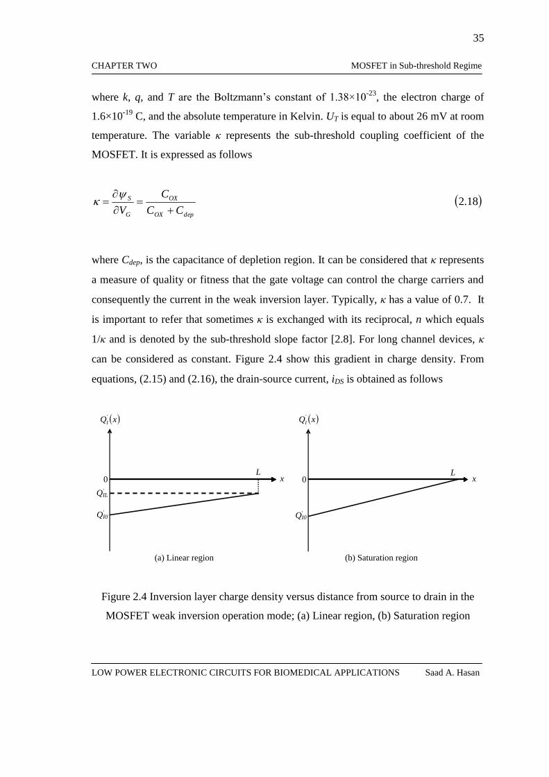
35
CHAPTER TWO MOSFET in Sub-threshold Regime
LOW POWER ELECTRONIC CIRCUITS FOR BIOMEDICAL APPLICATIONS Saad A. Hasan
where k, q, and T are the Boltzmann‟s constant of 1.38×10⁻²³
, the electron charge of
1.6×10⁻¹⁹
C, and the absolute temperature in Kelvin. UT is equal to about 26 mV at room
temperature. The variable κ represents the sub-threshold coupling coefficient of the
MOSFET. It is expressed as follows
18.2depOX
OX
G
S
CC
C
V
where Cdep, is the capacitance of depletion region. It can be considered that κ represents
a measure of quality or fitness that the gate voltage can control the charge carriers and
consequently the current in the weak inversion layer. Typically, κ has a value of 0.7. It
is important to refer that sometimes κ is exchanged with its reciprocal, n which equals
1/κ and is denoted by the sub-threshold slope factor [2.8]. For long channel devices, κ
can be considered as constant. Figure 2.4 show this gradient in charge density. From
equations, (2.15) and (2.16), the drain-source current, iDS is obtained as follows
x
0L
(b) Saturation region
x
xQI
'
0L
'QI0
'QIL
'QI0
(a) Linear region
xQI
'
Figure 2.4 Inversion layer charge density versus distance from source to drain in the
MOSFET weak inversion operation mode; (a) Linear region, (b) Saturation region

36
CHAPTER TWO MOSFET in Sub-threshold Regime
LOW POWER ELECTRONIC CIRCUITS FOR BIOMEDICAL APPLICATIONS Saad A. Hasan
'
2 19IDS n T
Qi W U . a
x
b.QQUL
Wi IILTnDS 192'
0
'
c.Q
QQU
L
Wi
I
ILITnDS 1921
'
0
''
0
d
U
V
U
VVVV
Q
Q
T
DS
T
GSGD
I
IL 19.2expexp'
0
'
By substituting equation (2.19d) in (2.19c)
202exp1exp0 .U
V
U
VVI
L
Wi
T
DS
T
SG
DS
where I0 is a process dependent constant. For the NMOSFET, it is found as follows
212exp12
0 .U
VUCI
T
THTOXn
From equation (2.20) above, the last term is approximately unity for the value of
VDS>4UT where the error is less than 2%. So, equation (2.20) can be simplified to be as
follows
222exp0 .U
VVI
L
Wi
T
SG
DS
It is interesting to see that equation (2.22) shows the drain-source current
independence of VDS. Therefore, the required condition for the MOSFET to operate in
saturation region in sub-threshold regime is to ensure that VDS>4UT. Hence, VDS of only

37
CHAPTER TWO MOSFET in Sub-threshold Regime
LOW POWER ELECTRONIC CIRCUITS FOR BIOMEDICAL APPLICATIONS Saad A. Hasan
100 mV is needed for MOSFET to operate as a current source in this regime. The bulk
potential affects the threshold voltage and from equations (2.21) and (2.22) above, the
drain-source current is affected. Assuming that all other potentials are constant, the
MOSFET drain-source current can be considered as a function of bulk potential which
becomes like a second gate in the MOSFET. Its effect in the small signal MOSFET
model can be modelled as a dependent current source of gmbvbs as shown in Figure 2.5
below. Therefore, Figure 2.5 represents the small signal MOSFET model in weak
inversion region with the parameters of gm, ro, and gmb expressed as follows
B.
-
vgs
G+
D
rO
.gmvgs gmbvbs
.
S
. .
-vbs
+
.
Figure 2.5 MOSFET small-signal model
23.2
tan,
T
DS
tconsvvGS
DS
mU
I
v
ig
BSDS
24.21
tan,
T
DS
OXdep
dep
T
DS
tconsvvBS
DS
mbU
I
CC
C
U
I
v
ig
GSDS
25.2,exp
exp0
tan,
DSATDS
T
DS
T
T
SG
tconsvvDS
DS
ds VVU
V
U
U
VVI
L
W
v
ig
GSBS

38
CHAPTER TWO MOSFET in Sub-threshold Regime
LOW POWER ELECTRONIC CIRCUITS FOR BIOMEDICAL APPLICATIONS Saad A. Hasan
In equation (2.25) above, the gds should reach to zero at saturation since the last
exponential term approaches zero for VDS ≥100mV. However, gds still has a finite value
beyond saturation due to the Early effect as in equation (2.26) below
26.2,1
DSATDS
T
DS
O
ds VVU
I
rg
where
dsDSDS iIi
27.2gsGSGS vVv
bsBSBS vVv
dsDSDS vVv
In equation (2.27) above, the capital letters and subscripts refer to the DC
operation while the small letters and subscripts refer to the small signal ac operation.
The summations of them reflect the normal operation with voltage and current values of
DC large signal components with small signal ac deviations around them.
2.3 The Test Chip
2.3.1 Introduction
The test chip is shown in Figure 2.6 below. It is fabricated in the AMS mixed
signal process using 0.35µm, double poly, 3 metal, CMOS C35 Technology and has
dimensions of 2.6mm×2.6mm. It consists of many circuits represented by three groups of
MOSFETs, various OTAs, proposed OTA-C filter topologies, a 4-channel filter bank for
hearing aids, and an OTA-C filter for EEG applications as detailed in next sections.

39
CHAPTER TWO MOSFET in Sub-threshold Regime
LOW POWER ELECTRONIC CIRCUITS FOR BIOMEDICAL APPLICATIONS Saad A. Hasan
Figure 2.6 2.6mm×2.6mmm Fabricated test chip
2.3.2 Architecture
The test chip blocks labelled 1-11 are explained as follows;
1. 1st group of 12 test MOSFETs with three different aspect ratio of (6 µm /6 µm), (30
µm /6 µm), and (12 µm /12 µm) for each four MOSFETs.
2. The 4-channel OTA-C band-pass filter bank.
3. 2nd
group of 6 test MOSFETs with three different aspect ratio of (6 µm /6 µm), (30
µm /6 µm), and (12 µm /12 µm) for each two MOSFETs.
11
1
2
3
10
5
6 9
7 8
4

40
CHAPTER TWO MOSFET in Sub-threshold Regime
LOW POWER ELECTRONIC CIRCUITS FOR BIOMEDICAL APPLICATIONS Saad A. Hasan
4. The proposed OTA-C band-pass filter topology 1 for hearing aids. The proposed
OTA MOSFETs dimensions are mentioned in table (3.1).
5. Another proposed OTA-C band-pass filter topology 1 for hearing aids with another
OTA dimensions. Those are represented by (15 µm /3 µm) for differential and
mirror MOSFETs, (30 µm /3 µm) for bumping MOSFETs, and (30 µm /6 µm) for
bias MOSFET.
6. The proposed OTA-C band-pass filter for EEG applications.
7. The proposed OTA for hearing aids.
8. The proposed OTA for EEG applications.
9. Different OTAs represented by the simple OTA and the OTA with bumping
MOSFETs.
10. 3rd group of 12 test MOSFETs with three different aspect ratio of (6 µm /6 µm), (30
µm /6 µm), and (12 µm /12 µm) for each four MOSFETs.
11. The proposed OTA-C band-pass filter topology 2 for hearing aids.
The measured output and transfer characteristics to the MOSFET groups will be
presented in the next section. Also, they will be compared with simulation results. The
other details including the measured results related with the proposed OTA, the OTA-C
filters and filter bank for hearing aids, and the OTA-C filter for EEG applications will
be presented in chapters three, five, and six respectively.

41
CHAPTER TWO MOSFET in Sub-threshold Regime
LOW POWER ELECTRONIC CIRCUITS FOR BIOMEDICAL APPLICATIONS Saad A. Hasan
2.4 Measured and simulated MOSFETs transfer characteristics
The transfer characteristics for the MOSFETs were obtained using the
Semiconductor Parameter Analyzer 4155B with VDS set at 0.1V. The simulated results
for the MOSFETs were obtained using Cadence circuit simulator, SpectreS with
BSIM3v3.1 models and parameters from the AMS process for 0.35µm CMOS C35
Technology. Some of these parameters are presented in Table 2.1 below.
Table 2.1: Key device parameters for BSIM3v3.1 model in AMS process for 0.35µm
CMOS C35 Technology
Description Symbol Unit NMOST PMOST
Gate oxide Thickness TOX nm 7.57 7.75
Effective substrate
doping NCH
cm-3
2.61×10¹⁷
1.01×10¹⁷
Effective mobility µo cm2/Vs 475 148
Threshold voltage VTH0 V 0.49 -0.69
Flicker noise coefficient KF ____ 2.17×10⁻²⁶
1.19×10⁻²⁶
Gate-Oxide Capacitance COX F/µm2
4.5×10⁻¹⁵
4.4×10⁻¹⁵
2.4.1 Transfer Characteristics
Figure 2.7 shows the transfer characteristics for MOSFETs with W=6µm and
L=6µm at VDS=0.1V. The measured curve represents the mean for ten MOSFETs having
the same above dimensions. Four of those MOSFETs are of the 1st group at the left edge
of the chip “block 1”, the other two are of the 2nd
group “block 3” in middle of the chip.
The last four MOSFETs are of 3rd
group at the right side of the chip “block 10”. The

42
CHAPTER TWO MOSFET in Sub-threshold Regime
LOW POWER ELECTRONIC CIRCUITS FOR BIOMEDICAL APPLICATIONS Saad A. Hasan
mismatch in weak inversion is calculated as the standard deviation of results from those
ten curves and found equal to 2.5%.
Figure 2.7 Measured and simulated transfer characteristic for MOSFETs with W=6µm,
L=6µm and at VDS=0.1V
The measured curve shown below in Figure 2.8 represents the mean curve of the
ten MOSFETs in the three groups mentioned above but with different dimensions of
W=30µm and L=6µm at VDS=0.1V. The mismatch in the weak inversion region in this
case is 2%.
0 0.5 1 1.5 2 2.5 310
-14
10-12
10-10
10-8
10-6
10-4
Gate-Source Voltage VGS (V)
Dra
in C
urren
t ID
(A
)
Simulated at VDS= 0.1V
Measured at VDS= 0.1V
Sub-threshold

43
CHAPTER TWO MOSFET in Sub-threshold Regime
LOW POWER ELECTRONIC CIRCUITS FOR BIOMEDICAL APPLICATIONS Saad A. Hasan
Figure 2.8 Measured and simulated transfer characteristic for MOSFETs with W=30µm,
L=6µm and at VDS=0.1V
Transfer characteristics of Figures 2.7 and 2.8 are plotted in the same graphs with their
simulation counterparts and show good agreement. However the mismatch percentage is
expected to be very small between the simulated and measured curves in each Figure.
2.4.2 Sub-threshold swing
The sub-threshold slope is the slope of the current, IDS in the logarithmic scale versus
the gate-source voltage, VGS. The inverse of the sub-threshold slope called the sub-
threshold swing, S. It shows the required reduction in VGS value which in turn reduces
the sub-threshold current, IDS by one order of magnitude. So, its unit is mV/decade. It is
calculated as in equations (2.28) [2.6] and (2.29) [2.9] below
0 0.5 1 1.5 2 2.5 310
-14
10-12
10-10
10-8
10-6
10-4
10-2
Gate-Source Voltage VGS (V)
Dra
in C
urr
ent
ID (
A)
Simulated at VDS=0.1V
Measured at VDS=0.1V
Sub-threshold

44
CHAPTER TWO MOSFET in Sub-threshold Regime
LOW POWER ELECTRONIC CIRCUITS FOR BIOMEDICAL APPLICATIONS Saad A. Hasan
282)(log
.Id
dVS
DS
GS
29210ln .U
S T
According to equation (2.29) above, the ideal value of κ is 1 so that the optimal
value of S is 60mV/decade. A small S value implies low threshold voltage for the same
value of the sub-threshold leakage current. For bulk MOSFETs, κ does not reach 1 but
for fully depleted (FD) silicon-on-insulator (SOI) MOSFETs [2.10], it may approach to
1. The values of S for simulated and measured curves are calculated using equation
(2.28) since its required variables are obtained directly from Figures 2.7 and 2.8. The
error between simulated and measured results is also calculated using the following
relation in equation (2.30). Table 2.2 below shows the S values for both Figures with the
error found between simulated and measured results.
302%100 .resultsSimulation
resultsMeasuredresultsSimulationError
Table 2.2: S values for Figures 2.7 and 2.8 with the error
Figure
number
S
Simulated
(mV/decade)
S
Measured
(mV/decade)
Error in S
(%)
2.7 80 81.5 1.875
2.8 80 81 1.25

45
CHAPTER TWO MOSFET in Sub-threshold Regime
LOW POWER ELECTRONIC CIRCUITS FOR BIOMEDICAL APPLICATIONS Saad A. Hasan
From Table 2.2 above, it is obvious that S simulated value represents the typical
value for bulk MOSFET at room temperature. The measured S values are close to the
typical values in both Figures which results in small error.
From equation (2.29) above, κ values for the simulation and experimental cases
are calculated in Table 2.3 below utilising S values in Table 2.2 above.
Table 2.3: κ values for Figures 2.7 and 2.8 with the error
Figure
number
κ
Simulated
(mV/decade)
κ
Measured
(mV/decade)
Error in κ
(%)
2.7 0.748 0.734 1.87
2.8 0.748 0.74 1.06
The threshold voltage, VTH of the measured curve of Figure 2.7 which represents
the mean threshold of the ten MOSFETs is obtained. The same exercise is repeated for
the measured curve of Figure 2.8. Table 2.4 below shows the threshold voltages of the
measured curves of Figures 2.7 and 2.8 with the error compared with parameter used in
simulation.
Table 2.4: Threshold voltage for Figures 2.7 and 2.8 with the error
Figure
number
VTH
Simulated
(mV)
VTH
Measured
(mV)
Error in
VTH
(%)
2.7 490 499 1.83
2.8 490 496 1.22

46
CHAPTER TWO MOSFET in Sub-threshold Regime
LOW POWER ELECTRONIC CIRCUITS FOR BIOMEDICAL APPLICATIONS Saad A. Hasan
2.5 Conclusion
In this chapter the operation of the MOSFET in both strong and weak inversion
regions is presented and discussed. The derivations of the current-voltage equations are
mentioned. The test chip which contains the proposed circuits in this work is
introduced. The measurements for MOSFETs were made from both sides and the
middle of the chip, and a good agreement indicates a small degree of variability across
the wafer. The experimental transfer characteristics for those MOSFETs show small
mismatch. Also the mismatch between the experimentally measured and transfer
characteristics simulated with nominal values from the AMS foundry was very low. The
inverse of the sub-threshold slope parameter, S values were obtained for simulated and
measured curves. The calculations show S measured values in good agreement with
those of simulation. The variation between the threshold voltages of experimental and
simulation results is obtained. The good match between MOSFETs simulated and
measured features explains the low error percentages in S values which confirm that
match. Thus, the comparable simulated and measured results for the proposed OTA and
OTA-C filters in later chapters can be considered as a result of this match in MOSFETs
features.
References
[2.1] Allen, P. E. and Holberg, D. R., CMOS Analogue Circuit Design, 2nd edition,
Oxford University Press, 2002.
[2.2] E. Vittoz, "Very low Power Circuit Design: Fundamentals and Limits", Proceeding
ISCAS'93, pp. 1439-1442, Chicago, May 1993.

47
CHAPTER TWO MOSFET in Sub-threshold Regime
LOW POWER ELECTRONIC CIRCUITS FOR BIOMEDICAL APPLICATIONS Saad A. Hasan
[2.3] W. M. Coughran, W. Fichtner, and E. Grosse, “Extracting transistor changes from
device simulations by gradient fitting,” IEEE Transactions on Computer-aided
Design of Integrated Circuits and Systems - TCAD , vol. 8, no. 4, pp. 380-394,
1989.
[2.4] S. E. Laux, “Techniques for small-signal analysis of semiconductor devices,”
IEEE Transactions on Electronic Devices, vol. ED-32, pp. 2028-2037, 1985.
[2.5] Y. Tsividis, K. Suyama, “MOSFET modeling for analog circuit CAD: problems
and prospects,” IEEE Journal of Solid-State Circuits, vol. 29, no. 3, pp. 210
216, March1994.
[2.6] Y. Tsividis, Operation and Modeling of the MOS Transistor, Third Edition,
Oxford: Oxford University Press, 2011.
[2.7] Y. Taur and T. H. Ning, Fundamentals of Modern VLSI Devices, New York:
Cambridge University Press, 1998.
[2.8] Vittoz, E., “The Design of High-Performance Analogue Circuits on Digital Chips”,
IEEE Journal of Solid-State Circuits, vol. 20 , no.3, pp. 657-665, June 1985.
[2.9] D. Flandre, J. P. Colinge, J. Chen, D. De Ceuster, J. P. Eggermont, L. Ferreira, B.
Gentinne, P. G. A. Jespers, A. Viviani, R. Gillon, J. P. Raskin, A. Vander Vorst,
D. Vanhoenacker, and F. Silveira, “Fully-depleted SOI CMOS technology for
low-voltage low-power mixed digital/analog/microwave circuits,” Analog
Integrated Circuits Signal Processing, vol. 21, pp. 213–228, 1999.
[2.10] S. Krishnan, J. G. Fossum, P. C. Yeh, O. Faynot, S. Cristoloveanu, and J.
Gauthier, “Floating-body kinks and dynamic effects in fully depleted SOI

48
CHAPTER TWO MOSFET in Sub-threshold Regime
LOW POWER ELECTRONIC CIRCUITS FOR BIOMEDICAL APPLICATIONS Saad A. Hasan
MOSFETs,” in Proceedings of the IEEE International SOI Conference, pp. 10-
11, 1995.

49
CHAPTER THREE OTA Linearisation Techniques and the Proposed OTA
LOW POWER ELECTRONIC CIRCUITS FOR BIOMEDICAL APPLICATIONS Saad A. Hasan
CHAPTER THREE
OTA Linearization Techniques and the Proposed
OTA
3.1 Introduction
The CMOS operational transconductance amplifier, OTA represents the main
building block for many analogue VLSI systems. It consists of MOSFETs which are
essentially, voltage-controlled current source devices and can be considered as having
inherently, transconductance characteristics. The commonly used OTA configuration is
that with differential input voltage with a single or differential output current that can be
easily controlled by controlling its bias current.
3.2 The simple OTA
The simple OTA shown in Figure 3.1 consists of five MOSFETs in a differential
configuration. Two input MOSFETs M1 and M2 share equally the current of the bias
MOSFET “current sink MOSFET” represented by the current source IB. Finally there
are the two current mirrors MOSFETs M3 and M4 that perform the subtraction of
currents to create the output current, Iout [3.1] as follows
1.32
tanh
T
d
BoutU
VII

50
CHAPTER THREE OTA Linearisation Techniques and the Proposed OTA
LOW POWER ELECTRONIC CIRCUITS FOR BIOMEDICAL APPLICATIONS Saad A. Hasan
where IB, and Vd, are the OTA bias current and the differential input voltage which
equals (Vin1-Vin2) where Vin1 and Vin2 are the non-inverting and inverting input terminals.
The differential operation offers the advantages of rejection of common-mode signals
and of cancellation of the noise from the bias current MOSFET.
M1 M2
M4M3
VSSVSS
VDD
Iout
Vin2
IB
Vin1
Figure 3.1 Simple OTA.
A disadvantage of the simple differential OTA is represented by its limited input
linear range [3.2] which causes the OTA output current to be saturated by small
differential input voltage. This arises due to the exponential current-voltage relationship
in MOSFETs when operating in the sub-threshold regime mentioned in chapter two.
From chapter two in equation (2.23) below, the MOSFET transconductance, gm is as
follows
T
Dm
U
Ig

51
CHAPTER THREE OTA Linearisation Techniques and the Proposed OTA
LOW POWER ELECTRONIC CIRCUITS FOR BIOMEDICAL APPLICATIONS Saad A. Hasan
In the sub-threshold regime, the transconductance is a function of the MOSFET
drain current, ID and its sub-threshold coupling coefficient, κ. From equation (2.23)
which repeated above, it can be concluded that in sub-threshold regime, the value of gm
is known once the current, ID is known. It is easy to show that the transconductance, Gm
of the simple OTA of Figure 3.1 is as follows
2.32 T
B
d
out
mU
I
V
IG
It is worth noting that the input linear range of the simple OTA is ~ ±6mV. It
can be seen that the MOSFET and the simple OTA transconductances are the same
since the MOSFET drain-source current, IDS has half the value of the bias current, IB of
the OTA. The OTA transition frequency, fT which represents the bandwidth of the OTA
can be expressed as
3.32
1
Lout
TCr
f
where rout, CL are the total OTA effective small-signal load resistance and capacitance at
the OTA output node. The resistance rout is expressed as follows
4.31
42 dsds
outgg
r
where gds2 and gds4 are the drain-source conductances of the OTA MOSFETs M2 and
M4 respectively.
3.3 Techniques to increase the OTA linear range
A number of techniques had been proposed to increase the OTA input linear
range. Some of these techniques are summarised below and involve either widening the

52
CHAPTER THREE OTA Linearisation Techniques and the Proposed OTA
LOW POWER ELECTRONIC CIRCUITS FOR BIOMEDICAL APPLICATIONS Saad A. Hasan
tanh function of Eqn. 3.1, or decreasing the ratio of transconductance to bias current to
give a wider linear range.
3.3.1 Source Degeneration Technique
The technique of source degeneration is well known, and was first used in
vacuum-tube design; it was then referred to as cathode degeneration, and was described
in [3.3]. Later, it was used in bipolar amplifier design, where it is referred to as emitter
degeneration. The idea behind source degeneration is to convert the current flowing
through a MOS transistor into a voltage through a resistor or diode (or diode-connected
transistors), and then to feed this voltage back to the source of the transistor to decrease
it‟s current. Figure 3.2 shows four different techniques where source degradation is used
to improve linearity. The simplest technique is to include a resistor between the two legs
of a simple differential pair as shown in Figure 3.2 a. This technique effectively reduces
current in the differential pair M1 and M2 by reducing the differential input voltage.
Then the OTA transconductance gm is reduced to an effective transconductance,
gmeffective as follows
5.31 Rg
gg
m
m
effectivem
where R is the resistor of Figure 3.2 and needs to have a large value compared to 1/ gm
so as to reduce gm effective.
Figure 3.2 (b and c) show the 2nd
and 3rd
techniques which also use source
degradation with a transistor MSD5 or two transistors MSD5 and MSD6 to act as single or
double so-called „diffussors‟ respectively. The diffussor conductivity in Figure 3.2 b is
governed by both the potential VGC and m for the single diffussor, MSD5. On the other
hand, the conductivity of the double diffussor is set by m only. The factor m represents
the ratio of diffussor MOSFET “single diffusor” or MOSFETs “double diffusors” aspect

53
CHAPTER THREE OTA Linearisation Techniques and the Proposed OTA
LOW POWER ELECTRONIC CIRCUITS FOR BIOMEDICAL APPLICATIONS Saad A. Hasan
ratio to that of the differential MOSFETs. The linear range is increased by 8 fold and 4
fold for m values of 0.25 and 0.5 for single and double diffussors respectively [3.4].
This increase is obtained by setting the 2nd
derivative of their output current equations
shown below to be equal to zero. [3.5], [3.6]
6.32
tanh14
1tanh
2tanh 1
T
d
T
d
BoutU
V
mU
VII
7.3
2cosh2
2sinh
tanh2
tanh 1
T
T
d
T
d
Bout
U
Vdm
U
V
U
VII
However the disadvantage of the single diffusor technique is represented by the
need to incorporate additional circuitry to get an input signal level to be around VGC.
M1 M2
M4M3
VSSVSS
VDD
Iout
Vin1 Vin2
R
IB/2 IB/2
(a)

54
CHAPTER THREE OTA Linearisation Techniques and the Proposed OTA
LOW POWER ELECTRONIC CIRCUITS FOR BIOMEDICAL APPLICATIONS Saad A. Hasan
M1 M2
M4M3
VSS
VDD
Iout
Vin1 Vin2
IB/2 IB/2
VSS
VGC
VSS
(b)
MSD5
MSD5
VSS
MSD6
VSS
M1 M2
M4M3
VSSVSS
VDD
Iout
Vin1
IB/2 IB/2
Vin2
(c)

55
CHAPTER THREE OTA Linearisation Techniques and the Proposed OTA
LOW POWER ELECTRONIC CIRCUITS FOR BIOMEDICAL APPLICATIONS Saad A. Hasan
(d)
M1 M2
M4M3
VSSVSS
VDD
Iout
Vin1 Vin2
IB
MSD5 VSSMSD6VSS
Figure 3.2 Source degradation linearization techniques for the simple differential OTA;
(a) Single resistor diffuser; (b) single MOSFET diffuser; (c) double MOSFETs
diffusers; (d) diode connected MOSFETs.
Figure 3.2 d shows the 4th source degeneration technique. It is represents simple
OTA differential pair with a diode connected source degradation transistor in each of its
two branches. The diode connected transistor has the effect of reducing the
transconductance by decreasing кe, the effective value of electrostatic coupling
coefficient “ratio” between the gate and channel as mentioned earlier in chapter one
[1.28]. Hence, к shifted by substrate bias and given as follows
8.32
tanh
T
de
BoutU
VII

56
CHAPTER THREE OTA Linearisation Techniques and the Proposed OTA
LOW POWER ELECTRONIC CIRCUITS FOR BIOMEDICAL APPLICATIONS Saad A. Hasan
9.3
diodes SD two 1
diode SD one 1
diodes no
2
3
2
e
As shown in equation (3.9), by using two source degeneration diode-connected
transistors, MSD5 and MSD6, placed as one transistor per branch, кe is decreased and the
linear range of the OTA becomes more than double that of the simple OTA. If the number
of diode-connected transistors is increased to four (two transistors per side), the linear
range will be increased by more than four times that of the simple OTA. The price is the
necessary increase in the minimum supply voltage and a decrease of the common-mode
operating range because MSD5 and MSD6 add an additional series voltage drop between the
differential pair M1 and M2 and the current sink, IB. In addition, there is an increase in
thermal intrinsic noise as a result of increasing the number of noise sources, represented
by MSD5 and MSD6.
3.3.2 Bumping MOSFETs Technique
Bumping is a technique for linearising the tanh function that presented in
equation (3.1) and hence extending the linear range of a sub-threshold differential pair
[3.8].
As shown in Figure 3.3 below, a bump differential OTA consists of three legs
two outer legs represent the simple differential pair of M1 and M2. A middle leg
containing two series connected transistors MB5 and MB6, operate as a simple current
correlator to the circuit [3.9].
The current through the transistors in the middle leg is a bump-shaped function
of the differential voltage, Vd centred around the origin. Thus, the differential output

57
CHAPTER THREE OTA Linearisation Techniques and the Proposed OTA
LOW POWER ELECTRONIC CIRCUITS FOR BIOMEDICAL APPLICATIONS Saad A. Hasan
current Iout from the outer two legs, is the usual tanh like function of the differential
input voltage Vd except for a region near the origin as in equation (3.1), where the bump
transistors are in conduction and they steal current, such that they take a bump current
away from the tanh like current function of the differential pair outer legs. It can be
shown that the current flowing through the bump transistors is represented as in
equation (3.10) [3.9] below
10.3
2cosh
41 2
T
d
Bbump
U
V
St
II
M1 M2
M4M3
VSSVSS
VDD
Iout
Vin1 Vin2
IB
MB5
MB6VSS
VSS
-VDD
Figure 3.3 Simple OTA with bumping MOSFETs technique of linearisation.
The bump transistors have no detrimental effect on the power consumption or
supply voltage required since they only add two transistors in series, and the currents in

58
CHAPTER THREE OTA Linearisation Techniques and the Proposed OTA
LOW POWER ELECTRONIC CIRCUITS FOR BIOMEDICAL APPLICATIONS Saad A. Hasan
the outer leg and central bump transistors sum to IB. The strength, St is the ratio of W/L
of the bump transistors MB5 and MB6 to that of M1 and M2 in the outer legs as in
equation (3.11) below
11.3
/
/
. pairdiff
bump
LW
LWSt
Hence, by controlling St, the properties of the OTA Iout -Vd curve can be controlled.
From equation (3.10) above, the effect of the bump transistors on the overall OTA
output current can be computed as follows
12.3cosh
sinh
2sec
41
2tanh
2x
x
U
Vh
St
U
VI
I
T
d
T
dB
out
where
T
d
U
Vx
St and
21
A small St does not significantly affect the OTA transfer characteristics and the
“Iout -Vd curve” and it essentially remains unchanged. A large St will cause a flat zone
near the origin. At intermediate values of St, the OTA expansive properties of its Iout -Vd
curve due to the bump compete with its compressive properties due to tanh. To obtain a
curve which is more linear than a tanh, the 2nd
derivative of equation (3.12) is obtained
and set to zero. The result represents the point of inflection which is at St = 2, resulting
in the maximally flat Iout -Vd curve at that point. The Taylor expansion of the output
current of the simple OTA is given as equation (3.13) while that of equation (3.12) after
putting bumping MOSFETs is in equation (3.14). It is obvious that equation (3.14) does
not contain a cubic distortion term [3.9]. The linearised function in equation (3.14) has a
5th
harmonic distortion term much less than that of equation (3.13). Bump linearisation

59
CHAPTER THREE OTA Linearisation Techniques and the Proposed OTA
LOW POWER ELECTRONIC CIRCUITS FOR BIOMEDICAL APPLICATIONS Saad A. Hasan
is a particularly useful technique because it increases the linear range of an OTA
without increasing its noise, since the transistors do not sit in the signal path.
14.37776045365403cosh2
sinh
13.340320
17
240
2
2422tanh
975
753
xxxx
x
x
xxxxx
3.3.3 Capacitor Attenuation Technique
This basic idea of attenuation is summarised by the placement of a voltage
divider at the OTA inputs to scale down the input voltage by a certain amount known as
the attenuation ratio. Figure 3.4 shows a simple OTA with capacitive dividers
represented by (C11/C12) and (C21/C22), connected to the non-inverting and inverting
terminals respectively. The capacitors serve to reduce the OTA transconductance by the
amount referred to as the attenuation ratio, and increase the linear range of the OTA by
that amount. In general, explicit capacitors can be used; an alternative is to employ a
multiple input, floating gate MOSFET. For the OTA constructed from floating gate
MOSFETs, the use of multiple input floating gate MIFG MOS transistor to increase the
transconductor linear range is feasible [3.10]. The MIFG MOSFET circuit provides
natural attenuation as a result of voltage division at its floating gate. Since the floating-
gate voltage of the MOS transistor is induced by multiple input voltages via double-poly
capacitors, the attenuation ratio and in turn the increase in the linear range can be
controlled by controlling the ratio of the capacitive divider [3.11].
However, there are some difficulties in this case which need additional care in
design and fabrication [3.12], [3.13]. They can be summarised as the follows.

60
CHAPTER THREE OTA Linearisation Techniques and the Proposed OTA
LOW POWER ELECTRONIC CIRCUITS FOR BIOMEDICAL APPLICATIONS Saad A. Hasan
M1 M2
M4M3
VSSVSS
VDD
Iout
IB
Vin1
C12
C11
C22
C21
Vin2
Figure 3.4 Simple OTA with capacitor attenuation technique
1. Effects of parasitic capacitances created between the MOSFET floating gate and
its four terminals. Also greater difficulty in alignment; errors due to geometric and
process parameter variation that may affect the capacitive ratio.
2. Effect of charge trapping in the floating gate that would induce an offset error on
the output current, requiring special techniques for removing it.
The linear range is increased by using the MOSFET bulk terminal as input. This
technique is known as bulk-driven technique. It can be thought as an implicit capacitive
divider since the gate, surface potential, and bulk of the MOSFET form three terminals
of a capacitive divider. In this technique, the bulk is chosen as an input instead of the
gate because the coupling ratio of the bulk to the surface potential of 1-к is less than that
of the gate represented by к. As a result, the transconductance of the bulk input becomes
less than that of the gate terminal. However, there are two main disadvantages in this

61
CHAPTER THREE OTA Linearisation Techniques and the Proposed OTA
LOW POWER ELECTRONIC CIRCUITS FOR BIOMEDICAL APPLICATIONS Saad A. Hasan
technique. The first one is the need to isolate the bulk terminals for all MOSFETs. The
second disadvantage is represented by the limited transition frequency, fT of the bulk-
driven MOSFET due to its high capacitance compared to that of the gate-driven
MOSFET [3.14]. This is less of a problem with the amplifiers operating in the audio
range, of interest here. It is important to mention that there are other techniques that can
be used to increase the linear range such as current division [3.15], current cancellation
[3.16], and using multiple asymmetric differential pairs [3.17]. These techniques all
require additional circuitry which compromises the footprint of the amplifier design
making them undesirable for the applications considered here.
3.4 A Review of Approaches to increase the Linear Range of OTA
A review of some of the aforementioned approaches used to increase the linear
range of the CMOS OTA reported in the literature, is summarized below
Fried et al in 1996 [3.7] proposed a technique for extending the linear range of
transconductors based on combining properly ratioed sub-threshold MOSFET
differential pairs in parallel. This is accomplished through the use of the bulk terminal
as an active terminal. This extends the linear range of the transconductors by a factor
close to 2. The linear range is increased to 250mVPP with the use of four parallel
differential pairs.
Grech et al in 2005 [3.18] proposed an OTA architecture with a novel bulk-input
differential pair using 0.7V supply. A tunable, wideband and compact designs with a
linear range of ±350mV was achieved. Two CMOS process were investigated for the
proposed OTA represented by 0.8 µm and 0.35 µm with threshold voltages of 0.7V and
0.5V respectively. The OTA total current was governed by the gate terminal via a
dummy pair. The OTA implemented using the 0.8 µm process, was used to implement a
2nd
order low-pass Gm-C filter for cochlear applications.

62
CHAPTER THREE OTA Linearisation Techniques and the Proposed OTA
LOW POWER ELECTRONIC CIRCUITS FOR BIOMEDICAL APPLICATIONS Saad A. Hasan
Hasler et al in 2006 [3.19] adopted the source degeneration and bump linearization
techniques to increase the linear input range of an OTA constructed from Fully
Depleted Silicon-On-Insulator (FD SOI) MOSFETS, used for hearing aids application.
An increase of the linear input range by a factor of 10 (from 12mVPP to 120mVPP)
compared with the simple OTA was established, whilst operating at a low voltage and
low current. With the increase in linearity, there was a trade-off between
transconductance bandwidth and noise. However for hearing aid applications, the need
to operate only at low frequency means that bandwidth was not considered a significant
issue. Simulations showed that use of the OTA within a first order CGm filter
operating on ± 1.5V could improve linearization of the dynamic range by up to 8dB.
C. D. Christopher in 2006 [3.1] proposed a wide linear range transconductance with a
high linear range of ±0.9V compared to ±75mV for the simple OTA. The explicit
capacitor attenuation technique was used for this purpose. A wide linear range OTA
was used to construct a cascaded differential attenuation filter to further increase the
linear range, to 1.414Vrms. The OTA-C band-pass filter operating in the sub-threshold
regime showed an experimental dynamic range of 60.8 dB using a supply voltage of
2.8V.
3.5 The Proposed OTA
Figure 3.5 shows the proposed OTA. It comprises of a simple differential OTA
circuit with bumping MOSFETs and capacitor attenuators. The bumping MOSFETs M5
and M6 are connected in series to each other and across the OTA rails. The linear range
is increased more than 4 fold with ideally, no noise cost. The capacitor attenuators are
represented by (C11/C12) and (C21/C22), connected to non-inverting and inverting OTA
terminals respectively. They represent explicit capacitive dividers which allows for
simple scaling of the attenuation ratio to adjust the linear range. Therefore, it is an
improvement compared to implicit attenuation of bulk-driven input technique. The

63
CHAPTER THREE OTA Linearisation Techniques and the Proposed OTA
LOW POWER ELECTRONIC CIRCUITS FOR BIOMEDICAL APPLICATIONS Saad A. Hasan
capacitive divider ratio in the latter case is determined by the physical parameters of the
process, and is intrinsically non-linear due to the dependence on parasitic depletion
capacitances of the MOSFET. Thus the divider ratio cannot be controlled
independently.
M5
M6
M1 M2
M7
M4M3
VSS
VSSVSS
VSS
VB
VSS
VDD
Iout
Vin2
C22
C21
Vin1
C12
C11
DC
VDD
DC
VSS
Figure 3.5 Proposed OTA
Also, the explicit capacitive divider is a passive element and linear for small signals
which means that the attenuation does not introduce harmonic distortion. The capacitor
attenuation ratio, a, is represented by the following equation
15.31
1
21
1
rCC
Ca

64
CHAPTER THREE OTA Linearisation Techniques and the Proposed OTA
LOW POWER ELECTRONIC CIRCUITS FOR BIOMEDICAL APPLICATIONS Saad A. Hasan
where r=C2/C1, the number of times that C2 is bigger than C1. Consequently the effective
value of the OTA transconductance, Gm effective using capacitor attenuators [3.18], [3.20]
will be as in equation (3.16)
16.3) meffectivem aGG
As a consequence, the input linear range is increased by a factor of a-1
. The capacitor
values of the proposed OTA are C11=C12= 0.5pF and C21=C22= 7.5pF. So, the increase in
linear range with these capacitor values is 16 fold. The proposed OTA with the
combination of both bump linearization and capacitor attenuation together for the first
time, offers a simple OTA structure with a minimum number of MOSFETs stacked
between its rails. The supply voltages VDD and VSS are +1.5V and -1.5V respectively. It
will be shown later, that the input linear range of this design is ±900mV at THD<5%.
3.6 MOSFET Sizing
Recently two approaches have become widely used as unified synthesis
methodologies valid in all regions of operation for determining MOSFET sizing and are
now described. The new approaches are based on analysis rather than tool-based
synthesis related with the conventional analogue design methods which require
complicated synthesis tools, SPICE like and simulators models, analytical or quick hand
methods for analogue circuits synthesise.
3.6.1 The gm / ID methodology
The gm/ID method for designing micro-power CMOS analogue circuits is
proposed in [3.21] and valid for all regions of operation of the MOSFET. Here mg stands
for transconductance of the MOSFET and ID its drain current. The normalized current IN

65
CHAPTER THREE OTA Linearisation Techniques and the Proposed OTA
LOW POWER ELECTRONIC CIRCUITS FOR BIOMEDICAL APPLICATIONS Saad A. Hasan
is defined as the ratio of the MOSFET drain current to its aspect ratio. Therefore, the
normalized current is given by
17.3)/( LW
II D
N
Both gm/ID and IN are independent of the transistor sizes, therefore the relation
between the two is unique for all transistors of the same type for a given fabrication
technology. It is worth noting that the validation of this methodology is evident for
long-channels for L values in the range of (3-12) µm, while some revision is needed for
short channel transistors [3.21]. The gm/ID versus IN relationship can be obtained either
by using transistor model equations or by experimentation. In the experimental case, the
gm/ID versus IN curves for many transistors needs to be obtained. Consequently, their
mean gm/ID versus IN curve used to consider the technology spreads [3.22].
The plot of the gm/ID ratio versus the normalized current, IN is used to calculate
MOSFET aspect ratios, W/L. Then by choosing the suitable length which represents the
compromise between the transistor area and stability on the one hand and dc gain on the
other hand, the MOSFET width, W can be found [3.23].
The gm/ID ratio in that plot is chosen according to the required region of
operation of the MOSFET. After making a projection of gm/ID on that plot, the
normalised current is obtained. In other words for the given values for any two of gm/ID,
gm, ID variables; W/L is determined directly. Finally, equation (3.17) is used to find W/L
since the required value of ID is known. The gm/ID versus ID/(W/L) curve is obtained and
shown in section 3.7 later. The total supply current is chosen and the drain of each
transistor can then be found. Using the value of ID with an appropriate value of gm/ID
based upon the desired operating regime of the transistor, allows the W/L ratio to be
determined. Therefore the primary variables in the synthesis process are the drain
currents of each transistor and their preferred gm/ID ratios. The maximum value of gm/ID

66
CHAPTER THREE OTA Linearisation Techniques and the Proposed OTA
LOW POWER ELECTRONIC CIRCUITS FOR BIOMEDICAL APPLICATIONS Saad A. Hasan
is limited firstly, by the weak inversion maximum value of the technology (about 35V-1
in thin film fully-depleted SO1 MOS transistors and less than 30V-1
in bulk MOS
transistors) and secondly, by the stability requirements because as gm/ID increases, with
fixed current, ID the transistor sizes and parasitic capacitances are increased and the
phase margin is reduced [3.21]. It is important to mention that this methodology is
adopted when sizing the MOSFETs in this work. The table containing the dimensions of
the MOSFETs for the proposed OTA will be presented in the later sections. The
MOSFETs dimensions are calculated by considering all MOSFETs to be operating in
the weak inversion region.
3.6.2 The Inversion Coefficient Approach
This methodology is proposed in [3.24] and is based on the concept of „level of
inversion‟. When the level of inversion is known, it can be used as the design variable
for optimising circuit parameters [3.24], [3.25]. The design degree of freedom in this
method is three, represented by the drain current ID, transistor length L, and so-called
inversion coefficient, IC. The EKV MOS model is the most appropriate model to work
with this approach. This model is continuous and valid in all regions of MOS operation,
and can be used for correlating the three degrees of freedom. The inversion coefficient,
IC can be expressed as follows
18.3)/(2)/(2
22
TO
D
TOXO
D
ULWnk
I
ULWCn
IIC
where µO is the low-field mobility and kO=µOCOX. Hence, IC is as follows
19.3)/( LWI
IIC
O
D
where IO is a process dependent current equals to 2nkOUT
2. The most convenient method
for interpreting the inversion coefficient is by making use of the gm/ID ratio.

67
CHAPTER THREE OTA Linearisation Techniques and the Proposed OTA
LOW POWER ELECTRONIC CIRCUITS FOR BIOMEDICAL APPLICATIONS Saad A. Hasan
3.7 Simulation Results
3.7.1 OTA MOSFETs sizing utilising gm/ID methodology
The simulations were conducted in the Cadence environment, using circuit
simulator, SpectreS with BSIM3v3.1 models and parameters from the AMS process for
0.35µm CMOS C35 Technology. According to gm/ID methodology, the MOSFET
dimensions are obtained after specifying the operation regime on the gm/ID versus
ID/(W/L) curve. For the proposed OTA, all its MOSFETs are operated in the sub-
threshold regime which is represented by high gm/ID values on the gm/ID versus ID/(W/L)
curve. The gm/ID versus ID/(W/L) curve can not be obtained directly. In this work it is
obtained by simulation using both transfer characteristics and gm/ID versus VGS curves
for the NMOS and PMOS transistors. For the gm/ID versus VGS curve, its x-axis
represented by VGS is exchanged with its corresponding ID values from the transfer
characteristics curve. In this way, the gm/ID versus ID curve is obtained. It should be
remembered that the x-axis should represent the normalised values of ID. This implies
the need to divide by the MOSFET aspect ratio, W/L used in obtaining its transfer
characteristics unless it equals 1. Hence, the gm/ID versus ID/(W/L) curve is obtained.
Figure 3.6 below shows these curves and also the final gm/ID versus ID/(W/L) curves for
both NMOS and PMOS transistors put in the same graph. Table 3.1 below presents the
MOSFETs gm/ID values chosen for the required sub-threshold operation with their
appropriate drain current, ID length, L and width, W values.

68
CHAPTER THREE OTA Linearisation Techniques and the Proposed OTA
LOW POWER ELECTRONIC CIRCUITS FOR BIOMEDICAL APPLICATIONS Saad A. Hasan
0 0.5 1 1.5 2 2.5 310
-12
10-10
10-8
10-6
10-4
Source-Gate Voltage VGS (V)
(a)
Dra
in C
urr
ent
ID (
A)
NMOSFET
0 0.5 1 1.5 2 2.5 30
5
10
15
20
25
30
Source-Gate Voltage VGS (V)
(b)
gm
/ID
(m
ho
/A)
NMOSFET

69
CHAPTER THREE OTA Linearisation Techniques and the Proposed OTA
LOW POWER ELECTRONIC CIRCUITS FOR BIOMEDICAL APPLICATIONS Saad A. Hasan
-3 -2.5 -2 -1.5 -1 -0.5 010
-12
10-10
10-8
10-6
10-4
Source-Gate Voltage VGS (V)
(c)
Dra
in C
urr
ent
ID (
A)
PMOSFET
-3 -2.5 -2 -1.5 -1 -0.5 00
5
10
15
20
25
30
Source-Gate Voltage VGS (V)
(d)
gm
/ID
(m
ho
/A)
PMOSFET

70
CHAPTER THREE OTA Linearisation Techniques and the Proposed OTA
LOW POWER ELECTRONIC CIRCUITS FOR BIOMEDICAL APPLICATIONS Saad A. Hasan
Figure 3.6 gm/ID versus ID/(W/L) curve; (a) NMOSFET transfer characteristics, (b) gm/ID
versus VGS curve for NMOSFET, (c) PMOSFET transfer characteristics, (d) gm/ID
versus VGS curve for PMOSFET, (e) gm/ID versus ID/(W/L) curves for NMOS and PMOS
transistors
Table 3.1: The dimensions of MOSFETs of the proposed OTA
MOSFET gm/ID
(V-1
)
ID
(nA)
W/L W
(µm)
L
(µm)
M1, M2 27 80 2.5 15 6
M3, M4 23 80 2.5 15 6
M5, M6 27.2 80 5 30 6
M7 26 240 5 30 6
10-12
10-10
10-8
10-6
10-4
10-2
0
2.5
5
7.5
10
12.5
15
17.5
20
22.5
25
27.5
30
Normalised Current IN "ID/(W/L) (A)"
(e)
gm
/ID
(m
ho
/A)
NMOSFET
PMOSFET
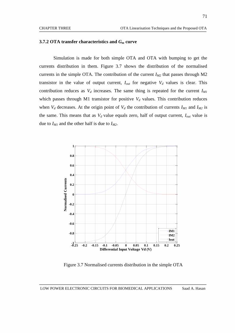
71
CHAPTER THREE OTA Linearisation Techniques and the Proposed OTA
LOW POWER ELECTRONIC CIRCUITS FOR BIOMEDICAL APPLICATIONS Saad A. Hasan
3.7.2 OTA transfer characteristics and Gm curve
Simulation is made for both simple OTA and OTA with bumping to get the
currents distribution in them. Figure 3.7 shows the distribution of the normalised
currents in the simple OTA. The contribution of the current IM2 that passes through M2
transistor in the value of output current, Iout for negative Vd values is clear. This
contribution reduces as Vd increases. The same thing is repeated for the current IM1
which passes through M1 transistor for positive Vd values. This contribution reduces
when Vd decreases. At the origin point of Vd the contribution of currents IM1 and IM2 is
the same. This means that as Vd value equals zero, half of output current, Iout value is
due to IM1 and the other half is due to IM2.
Figure 3.7 Normalised currents distribution in the simple OTA
-0.25 -0.2 -0.15 -0.1 -0.05 0 0.05 0.1 0.15 0.2 0.25-1
-0.8
-0.6
-0.4
-0.2
0
0.2
0.4
0.6
0.8
1
Differential Input Voltage Vd (V)
No
rma
lise
d C
urr
ents
IM1
IM2
Iout

72
CHAPTER THREE OTA Linearisation Techniques and the Proposed OTA
LOW POWER ELECTRONIC CIRCUITS FOR BIOMEDICAL APPLICATIONS Saad A. Hasan
Figure 3.8 below shows the distribution of normalised currents in the OTA with
bumping MOSFETs. For Figure 3.8, the contribution of IM1 and IM2 is relatively the
same when Vd value is far away from the origin. Near the origin, the influence of
bumping current, IBump due to bumping MOSFETs becomes clear as discussed earlier in
section 3.3.2. As Vd value equals zero, a maximum contribution of bumping MOSFETs
takes place. The contribution of the currents in each one of the three arms is the same in
the value of output current, Iout. This means that at zero Vd, IM1 IM2, and IBump are equal
and each one of them is one third the output current, Iout. The slope of the output current
Iout curve in its linear region in Figure 3.8 is less than that of the simple OTA of Figure
3.7. This is due to bumping MOSFETs effect that makes that slope which represents its
transconductance 2/3 times that of the simple OTA.
Figure 3.8 Normalised currents distribution in OTA with bumping MOSFETs with
aspect ratio of bumping MOSFETs double that of input MOSFETs
-0.25 -0.2 -0.15 -0.1 -0.05 0 0.05 0.1 0.15 0.2 0.25-1
-0.8
-0.6
-0.4
-0.2
0
0.2
0.4
0.6
0.8
1
Differential Input Voltage Vd (V)
No
rma
lise
Cu
rren
ts
IM1
IM2
IBump
Iout

73
CHAPTER THREE OTA Linearisation Techniques and the Proposed OTA
LOW POWER ELECTRONIC CIRCUITS FOR BIOMEDICAL APPLICATIONS Saad A. Hasan
Figure 3.9 presents the transfer characteristics of the simple, bumped, and
proposed OTAs. The effect of the linearisation techniques used is obvious in preventing
the proposed OTA output current from becoming saturated even at differential input
voltages of about ±1V.
Figure 3.9 Transfer characteristics of simple, bumped, and the proposed OTAs
The Gm curves for the simple, bumped, and proposed OTAs are shown in Figure
3.10 below
-1.5 -1.25 -1 -0.75 -0.5 -0.25 0 0.25 0.5 0.75 1 1.25 1.5-1
-0.8
-0.6
-0.4
-0.2
0
0.2
0.4
0.6
0.8
1
Differential Input Voltage Vd (V)
No
rma
lise
d O
utp
ut
Cu
rren
t Io
ut
(A)
Simple
Bump
Proposed

74
CHAPTER THREE OTA Linearisation Techniques and the Proposed OTA
LOW POWER ELECTRONIC CIRCUITS FOR BIOMEDICAL APPLICATIONS Saad A. Hasan
Figure 3.10 Normalised Gm versus Vd curves representing the input linear range of the
simple, bumped, and the proposed OTAs
According to simulations, the bias current, IB range of the proposed OTA is
shown in Table 3.2 below. It corresponds to the indicated transition frequency, fT range
for the two extremes of its linear region of operation represented by the ±900mV.
Table 3.2: The simulated IB and fT ranges of the proposed OTA
Parameter Value Unit
IBmin 0.5 nA
IBmax 570 nA
fTmin 5.3 kHz
fTmax 2.53 MHz
-1.5 -1.25 -1 -0.75 -0.5 -0.25 0 0.25 0.5 0.75 1 1.25 1.50.5
0.55
0.6
0.65
0.7
0.75
0.8
0.85
0.9
0.95
1
Differential Input Voltage Vd (V)
No
rma
lise
d T
ran
sco
nd
uct
an
ce G
m
Simple OTA
OTA with Bump
Proposed OTA
(Bump+ Cap. Atten.)

75
CHAPTER THREE OTA Linearisation Techniques and the Proposed OTA
LOW POWER ELECTRONIC CIRCUITS FOR BIOMEDICAL APPLICATIONS Saad A. Hasan
Table 3.3 shows the linear range obtained in this work compared with some
prior work of other researchers mentioned in section 3.4 above.
Table 3.3: A comparison of OTA input linear range using different linearisation
techniques
Ref. Technique Supply
Voltage
(V)
Linear
Range
Before
Linearisation
Linear
Range
After
Linearisation
[3.7] Source
degeneration, SD
of Fig. 3.2 (d)
-
≈ 24mVPP
250mVPP
at THD <1%
[3.18]
Bulk-driven Input
0.7
-
±350mV
[3.19]
SD of Fig. 3.2 (d)
+ Bumping
MOSFETs
±1.5
12mVPP
120mVPP
at THD <1%
[3.1] Capacitor
attenuation
2.8 75mV
±900mV
at THD <5%
[This
Work]
Bumping
MOSFETs
+ Capacitor
attenuation
±1.5
±6mV
±900mV
at THD <5%

76
CHAPTER THREE OTA Linearisation Techniques and the Proposed OTA
LOW POWER ELECTRONIC CIRCUITS FOR BIOMEDICAL APPLICATIONS Saad A. Hasan
The data in the table shows that the linear range obtained in this work is the largest one
besides that of [3.1]. The proposed OTA has the largest linear range enhancement ratio
among others.
3.8 Experimental Results
The proposed OTA is included on the test chip. The test chip shown in Figure
2.6 was fabricated in the AMS 0.35µm CMOS C35 technology process. The proposed
OTA occupies an area of 30,360µm2. The area of the capacitor attenuators is about
23,100µm2 which constitutes 76% of total area of the OTA.
Figure 3.11 shows the measured and simulated transconductance, Gm versus the
differential input voltage, Vd curve. The simulations were performed using nominal
values of transistor parameters supplied by AMS. It is worth noting that the fall-off in
the OTA transconductance is because of the influence of the transistors characteristics
especially their nonlinearities. The measured input linear range of about ±950mV at
THD<5%, or at 0.95 of its normalised amplitude confirms the simulation results and is
slightly larger than it.
In OTA-C filters, the nonlinearities can be explained sometimes due to the total
harmonic distortion, THD. However in OTA-C filters, most of harmonics are supposed
to be filtered. So, the THD measure for expressing nonlinearities sometimes is not
precise as for moderately nonlinear systems like square wave [3.1]. Besides, many
systems saturate when they become nonlinear and that is explained due to a gain
compression phenomenon. This is especially true for above-threshold systems with
large input signals as discussed in depth in [3.26].

77
CHAPTER THREE OTA Linearisation Techniques and the Proposed OTA
LOW POWER ELECTRONIC CIRCUITS FOR BIOMEDICAL APPLICATIONS Saad A. Hasan
Figure 3.11 Simulated and measured input linear range of the proposed OTA.
Figure 3.12 below reflects that variation in transconductance value with the
increase of the differential input voltage, Vd. It is obvious that when Vd exceeds the
OTA linear range, a large decrease in its Gm value takes place due to rise of
nonlinearity. It can also seen below in Figure 3.12 that the measured input linear range
of the proposed OTA is more than 950mV at a degradation percentage of 5% from its
maximum value for Vd range of (0-1)V.
-1.5 -1.25 -1 -0.75 -0.5 -0.25 0 0.25 0.5 0.75 1 1.25 1.50.5
0.55
0.6
0.65
0.7
0.75
0.8
0.85
0.9
0.95
1
Differential Input Voltage Vd (V)
No
rma
lise
d T
ran
sco
nd
uct
an
ce G
m
Simulated
Measured

78
CHAPTER THREE OTA Linearisation Techniques and the Proposed OTA
LOW POWER ELECTRONIC CIRCUITS FOR BIOMEDICAL APPLICATIONS Saad A. Hasan
Figure 3.12 The Measured variation percentage in the input linear range of the proposed
OTA.
Table 3.4 below presents the bias current, IB and transition frequency, fT ranges
for the proposed OTA within its measured linear region of ±950mV.
Table 3.4: The measured IB and fT ranges of the proposed OTA
Parameter Value Unit
IBmin 0.5 nA
IBmax 580 nA
fTmin 6.4 kHz
fTmax 2.56 MHz
0 0.1 0.2 0.3 0.4 0.5 0.6 0.7 0.8 0.9 10.5
1
1.5
2
2.5
3
3.5
4
4.5
5
Differential Input Voltage Vd (V)
Tra
nsc
on
du
cta
nce
Va
ria
tio
n P
erce
nta
ge
(%)

79
CHAPTER THREE OTA Linearisation Techniques and the Proposed OTA
LOW POWER ELECTRONIC CIRCUITS FOR BIOMEDICAL APPLICATIONS Saad A. Hasan
Table 3.4 shows relatively larger linear bias current and transition frequency
ranges compared to those obtained in simulation.
As it is essential to increase the input linear range of the OTA as discussed
above, it is also important to decrease its noise. The transistors sizing is very important
since it is related to the circuit area and performance including noise. The MOSFET
dimensions must be increased appropriately to reduce flicker noise. The MOSFET sub-
threshold operation brings the advantage of small input-referred white noise per unit
bandwidth since it is the regime of highest gm/ID values. The influence of noise on
design will be discussed in the next chapter as it represents the other half of the story in
low power applications. Therefore for a given power consumption, the sub-threshold
operation offers the more efficient MOSFET operation in terms of its noise and
bandwidth.
3.9 Conclusion
The upper input limit at which an OTA circuit operates properly without
distortion is represented by its input linear range. Some of the most commonly used
techniques to increase the OTA input linear range were presented and reviewed in this
chapter. The proposed OTA in this work was then presented. It has a simple structure
and a wide input linear range of ±900mVas a result of combining both bumping
MOSFETs and capacitive attenuation techniques together for the first time. The two
recent techniques used to describe the MOSFET behaviour in terms of modern analogue
design including the MOSFETs size calculation are discussed. The gm/ID methodology is
adopted for the calculations of MOSFET dimensions, exploiting the unique relation
between the MOSFET gm/ID ratio and the normalised drain current, ID/(W/L). This
approach provides an insight about a MOSFET-circuit performance during the design
stage. Experimental results were shown to confirm the design approach and showed
good agreement with those of simulation. Small discrepancies were explained by

80
CHAPTER THREE OTA Linearisation Techniques and the Proposed OTA
LOW POWER ELECTRONIC CIRCUITS FOR BIOMEDICAL APPLICATIONS Saad A. Hasan
reference to the larger input linear range, linear current range, and transition frequency
range.
References
[3.1] C. D. Christopher, Analog Adaptive Nonlinear Filtering and Spectral Analysis for
Low-Power Audio Applications, PhD thesis, Massachusetts Institute of
Technology, Massachusetts, 2006.
[3.2] P. Hasler, M. Kucic, and B. A. Minch, “A transistor-only circuit model of the
autozeroing floating-gate amplifier,” Circuits and Systems, 42nd
Midwest
Symposium, vol. 1, pp. 157-160, August 1999.
[3.3] R. W. Landee, D. C. Davis and A. P. Albrecht, Electronic Designers Handbook,
McGraw-Hill Book Co.: N. Y., pp. 3-18, pp. 3-34 to 3-38, 1957.
[3.4] P.M. Furth and A.G. Andreou, “Cochlear Models Implemented With Linearized
Transconductors,” Circuits and Systems, ISCAS, vol. 3, pp. 491-494, May, 1996.
[3.5] P.M. Furth. On the Design of Optimal Continuous-Time Filter Banks in
Subthreshold CMOS. PhD thesis, Johns Hopkins University, Baltimore, 1995.
[3.6] P.M. Furth and A.G. Andreou. Linearised differential transconductors in
subthreshold CMOS. Electronics Letters, vol. 31, no. 7, pp. 545-547, March,
1995.
[3.7] R. Fried and C. C. Enz, “Bulk-driven MOS transconductor with extended linear
range,” Electronic Letter, vol. 32, pp. 638–640, 1996.

81
CHAPTER THREE OTA Linearisation Techniques and the Proposed OTA
LOW POWER ELECTRONIC CIRCUITS FOR BIOMEDICAL APPLICATIONS Saad A. Hasan
[3.8] R. F. Lyon, T. Delbruck and C. A. Mead, "Circuits for wide input range analog
rectification and correlation", U.S. Patent 5319268, June 7th
, 1994.
[3.9] T. Delbruck, “Bump Circuits for Computing Similarity and Dissimilarity of
Analog Voltages,” CNS Memo 26, California Inst. Technol., Pasadena, May 24th
,
1993.
[3.10] J. Ramirez-Angulo, S. C. Choi and G. G. Altamirano, "Low Voltage Circuits
Building Blocks Using Multiple Input Floating Gate Transistors", IEEE
Transactions on Circuits and Systems-I, Vol. 42, pp. 971-974, November, 1995.
[3.11] S. Yan and E. Sanchez-Sinencio, “Low Voltage Analog Circuit Design
Techniques: A Tutorial”, IEICE Transactions on Fundamentals, vol. E83–A,
February, 2000.
[3.12] M. Pelgrom, A. Duinmaijer, and A. Welbers, “Matching propreties of MOS
transistors,” IEEE J. Solid-State Circuits, vol. 24, no. 5, 1989.
[3.13] C. Michael and M. Ismail, “Statical modeling of device mismatch for analog
MOS integrated circuits,” IEEE J. Solid-State Circuits, vol. 27, no. 2, pp. 152–
165, Feb. 1994.
[3.14] B.J. Blalock, P.E. Allen and G.A. Rincon-Mora, “Designing 1-V op amps using
standard digital CMOS technology”, IEEE Trans. Circuits and Systems – II, vol.
45, no. 7, pp. 769-780, July 1998.
[3.15] A. Veeravalli, E. S. Sinencio, and J. S. Martínez, “Transconductance Amplifier
Structures With Very Small Transconductances: A Comparative Design
Approach” Electronic Letters, vol. 31, no. 7, pp. 545–547, March 1995.

82
CHAPTER THREE OTA Linearisation Techniques and the Proposed OTA
LOW POWER ELECTRONIC CIRCUITS FOR BIOMEDICAL APPLICATIONS Saad A. Hasan
[3.16] S. S. Bustos, J. S. Martinez, F. Maloberti, and E. S. Sinencio, “A 60-dB dynamic-
range CMOS sixth-order 2.4 Hz Low-pass filter for medical applications”, IEEE
Trans. Circuits Syst.-II, vol. 47, no. 12, pp. 1391–1398, December, 2000.
[3.17] P. M. Furth, A. G. Andreou, “linearised differential transconductors in
subthreshold CMOS”, IEEE Trans. Circuits Syst.-II, vol. 47, no. 12, pp. 1391–
1398, December, 2000.
[3.18] I. Grech, J. Micallef, G. Azzopardi and C.l J. Debono, “A Low Voltage Wide-
Input-Range Bulk-Input CMOS OTA” Analog Integrated Circuits and Signal
Processing, vol. 43, no.2, pp. 127–136, May 2005.
[3.19] Hasler, O. Buiu B. Rue D. Flandre S. Hall, "Design of a low voltage - low
power, highly linear Fully-depleted SOI Operational Transconductance
Amplifier for Hearing Aid Applications," Journal of University of Liverpool,
2006.
[3.20] E. Sanchez-Sinencio and A. G. Andreou, ed., Low Voltage/Low Power Integrated
Circuits and Systems. IEEE Press, 1999.
[3.21] F.Silveira, D. Flandre and P. G. A. Jespers, "A gm/ID based methodology for the
design of CMOS analog circuits and its application to the synthesis of a silicon-
on-insulator micropower OTA", IEEE Journal of Solid-State Circuits, vol. 31,
no. 9, pp. 1314-1319, September 1996.
[3.22] F. Forty and M. E. Wright, “Measurement of MOS current mismatch in the weak
inversion region,” IEEE Journal of Solid State Circuits, vol. 29, no. 2, pp. 138-
142, February 1994.

83
CHAPTER THREE OTA Linearisation Techniques and the Proposed OTA
LOW POWER ELECTRONIC CIRCUITS FOR BIOMEDICAL APPLICATIONS Saad A. Hasan
[3.23] Fernando Paixao Cortes, Eric Fabris and Sergio Bampi, “Analysis and design of
amplifiers and comparators in CMOS 0.35µm technology”, Microelectronics
Reliability, vol. 44, no. 4, pp. 657-664, April 2004.
[3.24] Daniel Foty, David Binkley and Matthias Bucher, "Starting over: Gm/ID-Based
MOSFET Modeling as a Basis for Modernized Analog Design Methodologies",
University of North Carolina/Charlotte, Nanotech, vol. 1, no.13, pp. 682-685,
2002.
[3.25] D. M. Binkley, C. E. Hooper, S. D. Tucker, B. C. Moss, J. M. Rochelle, and D. P.
Foty, "A CAD methodology for optimizing transistor current and sizing in
analog CMOS design", IEEE Transactions on Computer-Aided Design of
Integrated Circuits and Systems, vol. 22, no. 2, pp. 225-237, 2003.
[3.26] S. Szczepanski and R. Schaumann, “Nonlinearity-induced distortion of the
transfer function shape in high-order OTA-C filters,” Analog Integrated Circuits
and Signal Processing, vol. 3, pp. 143-151, 1993.

84
CHAPTER FOUR Noise in Integrated Circuits
LOW POWER ELECTRONIC CIRCUITS FOR BIOMEDICAL APPLICATIONS Saad A. Hasan
CHAPTER FOUR
Noise in Integrated Circuits
4.1 Introduction
The word “noise” has an everyday use to refer for example to unwanted sound,
but in electrical engineering it has a specific meaning. Electrical noise represents the
unwanted current or voltage in an electrical circuit keeping in mind that real signals are
a sum of this unwanted signal “noise” and the desired signal [4.1]. It is a limiting factor
in system performance. It limits the minimum signal level that a circuit can handle with
acceptable quality. Attention is taken to deal with the problem of noise because it
constitutes a trade-off with power dissipation, linearity, and bandwidth.
The existence of noise is primarily due to the fact that electrical charge is not
continuous but is carried in discrete amounts equal to the charge of an electron which
leads to its association with the fundamental processes in the integrated circuit devices
[4.2]. It is important to study noise since it represents a lower limit to the size of
electrical signals which a circuit can process without significant deterioration in signal
quality.
In integrated circuits, noise phenomena can be assumed to be the result of small
current and voltage fluctuations that are generated within the devices themselves. Such
noise can be considered as intrinsic noise. In this chapter, the extraneous pick-up of
noise from external environment or sources which may cause problems for such low-
voltage low-power analogue circuits will not be discussed since it is outside the scope
of this study.

85
CHAPTER FOUR Noise in Integrated Circuits
LOW POWER ELECTRONIC CIRCUITS FOR BIOMEDICAL APPLICATIONS Saad A. Hasan
Unlike a deterministic process such as the output from a sine wave generator,
noise can be defined as a random process and its instantaneous value in time domain
cannot be predicted at any time when past values are known. Therefore noise should be
observed for a long period of time and can then be represented in a statistical model.
The model can be used to investigate other important noise properties rather than its
instantaneous amplitude. One of the important properties of noise which can be
predicted is its average power since most sources of noise in circuits exhibit a constant
average power. For circuits consisting of more than one noise source, it is usually
necessary to add the effect of all those sources to get the total noise contribution. This
superposition is usually used for deterministic voltages and currents. In analysing
random signals such as noise, basically the average noise power of two noise
waveforms represents the average of their summation. The summation can either be the
superposition of power if they are uncorrelated, such as noise produced by different
noise sources like a resistor and a transistor, or the average of their resulting power.
The latter adds another term represented by the correlation term of the two noise
waveforms. This refers to the case of correlated noise sources [see Appendix A].
The average power concept becomes more exploitable when identified with the
frequency content of noise. This is called the power spectral density, PSD which
represents the amount of power which the signal carries at each frequency. PSD is a
powerful tool for analysing the effect of noise in circuits as detailed in the next sections
[4.3].
4.2 Types of noise
Two different types of noise can corrupt analogue signals processed by integrated
circuits namely: device electronic noise and environmental noise. The latter refers to
random disturbances that a circuit may acquire through the supply or ground lines or the

86
CHAPTER FOUR Noise in Integrated Circuits
LOW POWER ELECTRONIC CIRCUITS FOR BIOMEDICAL APPLICATIONS Saad A. Hasan
substrate. Such noise is out of the study scope as mentioned in the introduction. The
device electronic noise is discussed below [4.3]
4.2.1 Thermal Noise
This type of noise appears in resistors due to the random motion of electrons in a
conductor that appears as a fluctuation in voltage even when the average current value
equals zero. It arises because the back and forth motion of electrons from the resistor to
the metal wire has a zero net charge transfer, but during a short time duration, a net,
non-zero current flow is probable. The thermal noise spectrum is proportional to
absolute temperature. This noise is represented by a series voltage source Thermalnv
___
,
2
or a
shunt current source Thermalni
___
,
2
[4.2] as follows
1.44___
2
, fkTRiThermaln
2.44___
2
, fR
kTv
Thermaln
where the over line in current and voltage equations indicates average values
k is the Boltzmann’s constant
T is the absolute temperature
R is the resistor value
Δf is the frequency bandwidth of interest in the Hz unit.
In the MOSFET, thermal noise also appears. The most significant source of
noise is that generated in channel. This noise can be modelled in long channel devices
operating in the saturation regime, as a current source connected between drain and

87
CHAPTER FOUR Noise in Integrated Circuits
LOW POWER ELECTRONIC CIRCUITS FOR BIOMEDICAL APPLICATIONS Saad A. Hasan
source terminals that has a mean squared value of Thermalni
___
,
2 or as a voltage source
Thermalnv___
,
2
connected in series to its gate as in Figure 4.1 with a mean squared values [4.4]
as explained in equations (4.3) and (4.4) respectively
(a) (b)
S
D
GThermalnv
___
,
2
Thermalni___
,
2
S
D
G *
Figure 4.1 Thermal noise representation of the MOSFET, (a) Thermal noise current
source (b) Thermal noise voltage source
3.44 0
___2
, fgkTi dsThermaln
4.44___
2
, fg
kTv
mThermaln
where gds0, γ, and gm are channel conductance at zero electric field and a coefficient
equal to ½ and 2/3 in the saturation region in sub-threshold and above-threshold
regimes respectively for long channel MOSFETs, and the transconductance in the
saturation region. For short channel MOSFETs, γ may take larger values [4.4].
Thermal noise has a flat frequency spectrum along the frequency bandwidth of interest,
Δf. Equations (4.3) and (4.4) show that MOSFETs operation at low temperature exhibits

88
CHAPTER FOUR Noise in Integrated Circuits
LOW POWER ELECTRONIC CIRCUITS FOR BIOMEDICAL APPLICATIONS Saad A. Hasan
lower thermal noise in analogue circuits. This approach becomes more attractive with
the observation that the charge carrier mobility in MOS devices increases at low
temperatures [4.5]. The other thermal noise source is represented by MOSFET ohmic
sections, especially the gate resistance. This additional thermal noise can be reduced by
careful layout.
4.2.2 Shot Noise
The shot noise is mainly associated with a direct current flow. It results from
discrete movement of charge across a potential barrier; it is present in diodes,
bidirectional junction transistors, and MOSFETs. It is a mean square value [4.6] as
follows,
5.42___
2 fqIfi Dshotn
where fishotn
___2 is the shot noise current source. For most practical electronic devices,
equation (4.5) is accurate well into the gigahertz region [4.2]. This is because equation
(4.5) is valid for frequencies to the inverse of the carrier transit time through the
depletion region, which is extremely small.
Each shot noise and thermal noise source can be represented by a white noise
power spectral density. This gives rise to the question of how to distinguish between
them and how to calculate white noise in MOSFETs for the present case of the sub-
threshold regime. It is interesting to note that the shot and thermal noise have long been
considered the results of two distinct mechanisms, but there is evidence that they are not
[4.6]. It can be shown theoretically and experimentally that the noise in MOSFETs
operating in the sub-threshold regime is essentially the sum of shot-noise components
from the forward and reverse currents which represent at the same time the total thermal

89
CHAPTER FOUR Noise in Integrated Circuits
LOW POWER ELECTRONIC CIRCUITS FOR BIOMEDICAL APPLICATIONS Saad A. Hasan
noise. This view of thermal noise as a two-sided shot-noise process is fundamental since
it introduces a unifying view of thermal noise and shot noise [4.6].
4.2.3 Flicker Noise
This type of noise is found in all devices from different kinds of resistors to
semiconductors. Because 1/f noise is well spread over the components, it is likely to be
caused by a fundamental physical mechanism. Physics based MOSFET noise model is
proposed in [4.7]. The model can predict the MOSFET noise features in sub-threshold,
linear and saturation regions of operation. The commonly accepted explanation of the
1/f noise is based on carrier number fluctuation theory [4.8]. The noise primarily arises
at the interface between the gate oxide and the silicon of MOSFET. Inside the gate
oxide, specifically near the interface between the gate oxide and silicon substrate, there
are energy states or “traps” due to impurities or oxygen vacancies. These traps randomly
capture and release charge carriers from the MOSFET channel causing electronic
fluctuations which constitutes such noise [4.2]. The oxide charge fluctuations
dynamically change the surface potential which changes the MOSFET threshold
voltage. For this reason, the flicker noise can also be considered as a result of
dynamically varying threshold voltage [4.9]. It is called flicker noise because when it
viewed in a light source, flickering is observed. Also it is denoted by pink noise (reddish
color present in the lower range of visible spectrum) and 1/f noise (because of its
inverse proportion to frequency). The existence of flicker noise can be also explained as
a result of transistors mobility fluctuations as described in the Hooge model [4.10].
The average power of flicker noise cannot be predicted easily as it is highly
dependent on processing and will show considerably variation from one CMOS
technology to another. It is considered as a series connected voltage source, fnv/
___
, 1
2 to
the MOSFET gate and modeled [4.9] as follows

90
CHAPTER FOUR Noise in Integrated Circuits
LOW POWER ELECTRONIC CIRCUITS FOR BIOMEDICAL APPLICATIONS Saad A. Hasan
6.4
1/1
___2
, ffWLC
Kv
OX
F
fn
KF, COX, W, and L are respectively the flicker noise constant which is process-
dependent, the oxide capacitance per unit area, the channel width, and the channel
length.
The inverse dependence of flicker noise on frequency shows clearly that this
type of noise has a great effect at low frequency response. The flicker noise is also
inversely proportional to MOSFET area, WL [4.9] which should therefore be made
large. This explains the reason for using MOSFET areas of several thousands of square
microns in low-frequency application circuits. It is important to notice that in order to
quantify the significance of 1/f noise with respect to thermal noise for a certain device,
both spectral densities of these noise sources should be plotted on the same axes as
shown in Figure 4.2 below. This concept is known as flicker noise corner frequency, fc.
2log20 nv
corner1
f
scale) (log f
Noise Thermal
Noise
Flicker
cf
Figure 4.2 Concept of flicker noise corner frequency

91
CHAPTER FOUR Noise in Integrated Circuits
LOW POWER ELECTRONIC CIRCUITS FOR BIOMEDICAL APPLICATIONS Saad A. Hasan
The corner frequency represents the intersection point in frequency axis at which
both noise power spectral densities have same value. So, the corner frequency will be a
measure of the part of frequency band that is mostly corrupted by flicker noise. It is
desirable to minimize fc to realise MOSFETs with low corner frequencies. The flicker
noise corner frequency, fc can be obtained as follows
cOX
F
m fWLC
K
g
kT 14
7.44
kT
g
WLC
Kf m
OX
Fc
From equation (4.7), fc mainly depends on device dimensions and drain current.
4.3 Representation of noise in circuits
The noise is estimated by setting the input to zero, then measuring the total noise
at the output due to the various sources of noise in the circuit. The noise is always
measured on the output of the circuit. The output-referred noise does not allow a fair
comparison of the performance of different circuits since it depends on the gain. It can,
however be referred back to the input of the circuit by dividing its value by the circuit
gain for comparison with an input signal. The input-referred noise is not physically
present which explains why it is impossible to calculate it directly or measure it at the
input of a circuit. This is especially true for CMOS circuits where the input to a circuit
may be the polysilicon gate of a MOSFET that is surrounded by an insulating dielectric.
For a noisy circuit of any source impedance, the input-referred noise can be modelled as
shown in Figure 4.3 below, by voltage and current sources connected respectively in
series and parallel to the input of a noiseless circuit. So, for the case of a low input
impedance circuit the noise current will have little effect on the circuit output which

92
CHAPTER FOUR Noise in Integrated Circuits
LOW POWER ELECTRONIC CIRCUITS FOR BIOMEDICAL APPLICATIONS Saad A. Hasan
makes the noise calculated at the output to be solely due to the noise voltage source.
For, a high input impedance circuit, the noise voltage source has little effect and the
noise calculated at the output is solely from the noise current source [4.1].
. .
.
.
.
innv___
2
,
inni___
2
,
Noiseless
Circuit
.
Figure 4.3 Representation of noise by voltage and current sources
Both input-referred noise voltage and current sources can be calculated due to
varying source impedances at the input terminal. Such a style of noise representation
complicates calculations. It is difficult to track the correlations between both input-
referred noise sources which are due to device noise in one transistor which may add
additional terms as mentioned earlier in section 4.1.
4.4 Another strategy of noise representation
Another strategy depends on whether the input is a source impedance voltage
input or a source admittance current input. As a consequence, the input referred voltage
noise in series with source impedance voltage input or the input referred current noise in
parallel with source admittance current input are calculated in accordance with the
actual input. Hence, the possibility of correlation disappears in this strategy since there
is only one input noise source.

93
CHAPTER FOUR Noise in Integrated Circuits
LOW POWER ELECTRONIC CIRCUITS FOR BIOMEDICAL APPLICATIONS Saad A. Hasan
In this strategy, superposition is used to calculate the noise power per unit
bandwidth separately due to each noise source by suppressing the contribution of other
sources each time. Then after calculating the power noise due to all noise sources
separately, the products of their mean square noise sources and the squared noise
transfer functions from their inputs to circuit output values are summed. The total
output noise is obtained by integrating the output noise power over all frequencies. The
output noise power can be referred back to the actual input by dividing its value by the
magnitude of the squared transfer function from that input to the output. In this fashion,
the source impedances effects are already taken into account automatically due
computing the transfer functions from input to output, and any noise power due to the
source impedance simply adds to the input-referred noise.
It is worth noting that this strategy considers that all noise sources from different
devices in a circuit are independent and uncorrelated during calculations. This belongs
to the assumption of small signal case where the net effect of all noise sources is still
small enough such that the operating point of the circuit is not significantly affected
[4.11]. In this work, the calculations of noise are made according to this strategy.
4.5 Noise for MOSFET and OTA
The noise relations for the MOSFETs and CMOS OTA are detailed in this
section as follows:
4.5.1 Noise model for MOSFET
The total noise power mean squared value, ___
2
nv in the MOSFET is represented by
summing the thermal noise Thermalnv
___2
and the flicker noise)/(
___
fnv1
2 as follows
HzVvvvfnThremalnn /)/(
_________2
1
222

94
CHAPTER FOUR Noise in Integrated Circuits
LOW POWER ELECTRONIC CIRCUITS FOR BIOMEDICAL APPLICATIONS Saad A. Hasan
8.4ln414___
2
L
H
OX
FLH
m
f
f
OX
Ff
f
m
nf
f
WLC
Kff
g
kTdf
fWLC
Kdf
g
kTv H
L
H
L
where the term(fH - fL) is the frequency bandwidth of interest, Δf since fH and fL are the
highest and lowest frequencies of interest respectively. The RMS value of the MOSFET
noise voltage, RMSnv , is calculated as follows
9.4ln4
___2
,
L
H
OX
FLH
m
nRMSnf
f
WLC
Kff
g
kTvv
It can be concluded from equations (4.8) and (4.9) above, that the thermal noise can be
reduced as gm is increased. This means noise is reduced at the expense of increasing the
bias current and hence increasing the power consumption. The price of reducing the
flicker noise is paid by increasing MOSFET dimensions which means expending more
area and by extension larger circuits.
4.5.2 Noise in the simple OTA circuit depending on strategy of 4.3
Figure 4.4 (a) shows the noise model of the simple OTA. The noise in each
MOSFET is represented by its input noise voltage generator described by equation (4.8)
above. The input-referred noise voltage innv
___
,
2
for the simple OTA is indicated in
equation (4.10) below and shown in Figure 4.4 (b).
10.4/2___
2
4
___2
3
2
1
3
___2
2
___2
1
___2
, HzVvvg
gvvv nn
m
mnninn

95
CHAPTER FOUR Noise in Integrated Circuits
LOW POWER ELECTRONIC CIRCUITS FOR BIOMEDICAL APPLICATIONS Saad A. Hasan
Here it has been assumed that gm1=gm2 and gm3=gm4, where gm1, gm2, gm3, and gm4
are the transconductances of the OTA MOSFETs M1, M2, M3 and M4 respectively.
Iout
M1 M2
M4M3
VSS
M7VB
VSS
VSS
VDD
*
(b)
M1 M2
M4M3
VSS
M7VB
VSS
VSS
VDD
Iout
**
**
___2
1nv___
2
2nv
___2
3nv___
2
4nv
innv___
,
2
(a)
Figure 4.4 Noise model of the simple OTA, (a) Taking the equivalent sources for each
MOSFET (b) The overall equivalent noise model for the simple OTA
From equation (4.10) it can be concluded that the input MOSFETs M1 and M2
contribute directly to the OTA noise while the contribution of mirror MOSFETs M3 and
M4 is related by the square of their transconductance ratio to that of the input
MOSFETs.
Assuming that: ______
2
2
2
1 nn vv and______
2
4
2
3 nn vv
Hence equation (4.10) is written as follows
11.4/22 2
2
1
3
___2
3
___2
1
___2
, HzVg
gvvv
m
mnninn

96
CHAPTER FOUR Noise in Integrated Circuits
LOW POWER ELECTRONIC CIRCUITS FOR BIOMEDICAL APPLICATIONS Saad A. Hasan
The importance of equation (4.11) in OTA design is represented by the ability to
consider the input-referred thermal noise and the input referred 1/f noise separately to
guide the choice of appropriate MOSFET sizing [4.2]. For above threshold operation,
the MOSFET transconductance, gm is related to its dimensions besides its drain current.
Therefore equation (4.11) can be rewritten to show the separated OTA thermal and
flicker input-referred noise respectively as in equations (4.12) and (4.13).
12.41
22
3
2
1
11/1
___2
, fLK
LK
CLfW
Kv
nFn
pFp
OX
n
fn
where KFp, KFn are the flicker noise coefficients in p-channel and n-channel MOSFETs
respectively.
Equation (4.12) above explains the equivalent input-referred flicker noise in the
simple OTA. The 1st term indicates the contribution of input MOSFETs in flicker noise
while the term in parenthesis shows that of the mirrors. The contribution of mirror
MOSFETs to flicker noise can be reduced by using longer channel devices than the
input counterparts.
13.4/
/1
/23
44
1
3
1
___2
, fLW
LW
ILWCkTv
p
n
DOXn
Thermaln
Equation (4.13) above explains the equivalent input-referred thermal noise in the
simple OTA. The 1st term in parenthesis shows the thermal noise contribution of input
MOSFETs. The 2nd
term in parenthesis indicates the thermal noise contribution of the
current mirror. Thus from equation (4.13), the mirror thermal noise contribution “the 2nd

97
CHAPTER FOUR Noise in Integrated Circuits
LOW POWER ELECTRONIC CIRCUITS FOR BIOMEDICAL APPLICATIONS Saad A. Hasan
term” can be reduced by choosing (W/L)1 > (W/L)3, i.e. making the input MOSFETs
with higher aspect ratio than mirror MOSFETs.
For the OTA operating in the sub-threshold regime, the MOSFET
transconductances are directly related to their drain currents. So, the mirror to input
MOSFETs transconductance ratio becomes 1. This is because the same currents are
flowing in either OTA branches. Thus the input and mirrors MOSFETs will contribute
all their noise to the OTA.
4.5.3 Noise in the sub-threshold simple OTA depending on strategy of 4.4
The sub-threshold OTA operates within its linear range region. The small signal
model of Figure 2.4 is adopted to represent each MOSFET in the OTA to derive its
input-referred noise power per unit bandwidth. Figure 4.5 below shows the small signal
noise circuit of the simple OTA.
From Figure 4.5 below, the output noise per unit bandwidth will now be determined
by superposition for each noise source separately assuming they are uncorrelated. This
is done by replacing the voltage sources with short circuits and the current sources with
open circuits. For this OTA, the contribution in output noise of each one of its five
MOSFETs is taken with the absence of other MOSFETs as follows

98
CHAPTER FOUR Noise in Integrated Circuits
LOW POWER ELECTRONIC CIRCUITS FOR BIOMEDICAL APPLICATIONS Saad A. Hasan
___2
1i
___2
2i
2xi
___2
3i
___
2
5i
1/gs
1/gm
1/gs
1xi
___2
4i
mi
outimi
1xi 2xi
Figure 4.5 Small signal noise circuit of the simple OTA
1. MOSFET, M1 small signal model represented by a dependent current source, Vs
gs. The parameter gs refers to the summation of MOSFET transconductance, gm and
bulk transconductance, gmb. It is more appropriate to use resistance instead of
transconductance in such calculations, so that the dependent current source, Vs gs is
replaced by a resistor, 1/gs and the dependent current source, ix1. Then the noise
independent current source ___
2
1i is placed across the M1 drain to source terminals. The
noise current, i1 is equally divided into the two resistors 1/gs. From Figure 4.5, the
current in each one of the two 1/gs resistors, ix1 and ix2 equals i1/2. The current passing
through mirror resistance, 1/gm is im which equals ix1-i1 then it equals -i1/2. The OTA
output current, iout equals ix2-im. So, iout = ix2-im = ix1- i1/2 = i1/2-(- i1/2) = i1, which means
that all the noise current of MOSFET, M1 is added to the OTA output. Hence, the

99
CHAPTER FOUR Noise in Integrated Circuits
LOW POWER ELECTRONIC CIRCUITS FOR BIOMEDICAL APPLICATIONS Saad A. Hasan
transfer function of the MOSFET, M1 from its input to the OTA output is α1 which
equals (1/2-(-1/2)). The squared value of the transfer function, 2
1 equals (1)2.
2. MOSFET, M2 is represented by its small signal model with the noise
independent current source,___
2
2i that is placed across its drain to source terminals. The
entire procedure made for M1 is repeated for M2, applied to mirror MOSFETs M3, M4,
and to the bias MOSFET, M5 as in Figure 4.5 above. The results of this exercise are
presented in Table 4.1 below
Table 4.1: Noise contribution and the noise transfer functions due to noise current
sources in the simple OTA
MOSFET Noise
current
source
iout = ix2- im
Due to each
noise current
source
Percentage
contribution to
the OTA output
noise (%)
Transfer
function 2
j
magnitude
(A/√Hz)
M1
___2
1i
i1/2-( i1/2)= i1
100
(½- (-½))2 =1
M2
___2
2i
-i2/2- i2/2= -i2
100
(-½-½)2 = 1
M3
___2
3i
-i3
100
(-1)2= 1
M4
___2
4i
i4
100
(1)2= 1
M5
___2
5i ix2- ix1= 0
0
(0)2= 0

100
CHAPTER FOUR Noise in Integrated Circuits
LOW POWER ELECTRONIC CIRCUITS FOR BIOMEDICAL APPLICATIONS Saad A. Hasan
From Table 4.1 above, it is clear that the input and mirror MOSFETs contribute
all their noise to the OTA output while, ideally, the bias MOSFET contributes no noise
due to opposing noise contributions from the two OTA arms. Hence, the total shot
“white” noise current per unit bandwidth, fiout
___2 at the OTA output equals
2201111 22222
___2
5
1
2_________
2 Bj
jjout
Iqfifi
where j represents the number of independent noise current sources.
14.42
24_________
2
B
out
Iqfi
Thus, the total noise current per unit bandwidth, ___________
, fi totout
2 due to both white and flicker
noise at the OTA equals
15.4/1
224 22
___________2
, HzAgfWLC
KIqfi m
OX
FBtotout
The input-referred noise voltage per unit bandwidth, __________
, fv inn
2 is obtained as follows
16.4/2
2
___________2
,__________
2
, HzVG
fifv
m
totout
inn
In general, for N shot noise sources, the input-referred noise in all frequencies can be
expressed as follows

101
CHAPTER FOUR Noise in Integrated Circuits
LOW POWER ELECTRONIC CIRCUITS FOR BIOMEDICAL APPLICATIONS Saad A. Hasan
17.42/
22
/
2
2
___2
, dfWLfC
IKIq
VI
Nv
OX
BFB
f LB
inn
l
where N, VL, and q are the effective number of shot-noise sources in the amplifiers, the
input linear range, and the charge on the electron respectively. 22
mLB GVI / as long
as the OTA operates within its linear range in the sub-threshold regime.
Finally, the RMS value of the noise voltage RMSeqnv ,, for the simple OTA is as follows
18.4___
2
,,, innRMSeqn vv
4.5.4 Noise in Cascaded Amplifiers
The output noise power and the input referred noise power of a cascade of M
noisy amplifiers shown in Figure 4.6 can be written as follows in equations (4.19) and
(4.20) respectively
19.4/
).....().....(
2
,
___2
,
2
,2
___2
,
2
2,1
___2
,
2
21,
_____2
HzV
vAvAAvAAAvRMSinMnvMRMSinnvMvRMSinnvMvvRMSout
where AV1, AV2, and AVM are the open loop voltage gains for M amplifiers shown in
Figure 4.6 below. The equivalent input-referred noise power, RMSeqinnv,,
___
,
2 is obtained as in
below
20.4/).....(
2
2
121
,
___2
,
2
1
,2
___2
,
,1
___2
,,,
___2
, HzVAAA
v
A
vvv
vMvv
RMSinMn
v
RMSinn
RMSinnRMSeqinn

102
CHAPTER FOUR Noise in Integrated Circuits
LOW POWER ELECTRONIC CIRCUITS FOR BIOMEDICAL APPLICATIONS Saad A. Hasan
Input * * *
*
2nd -Stage 1st -Stage Mth -Stage
(a)
(b)
Av1
Av1
Av2 AvM
Av2 AvM
vRMSinMn ,RMSinnv
,2RMSinnv,1
RMSeqinnv,,
Input
Output
Output
RMSoutv ,
RMSoutv ,
Figure 4.6 Noise performance of a cascade of amplifiers,(a) A cascade of noisy
amplifiers with their corresponding input-referred noise sources (b) The equivalent
noise model for (a).
From equation (4.20), it is clear that when the open loop voltage gains are greater
than unity, which is often the case; the early stages contribute more noise than the later
stages [4.11]. Thus the input-referred noise power of the 1st stage has the largest effect
on the noise performance of the system constituted from the M cascaded amplifiers. So,
care should be taken in designing the early stages since it has a crucial effect on the total
input-referred noise of such system and hence its dynamic range.
4.5.5 Noise in a system consisting of a feedback loop
Before mentioning the effect of the system with a feedback loop on the noise, the
closed loop transfer function of a simple linear system consisting of a negative feedback
loop is derived. The system block diagram consists of a(s) and f(s), the feed forward and
the feedback stages as shown in Figure 4.7 below. In such systems, the negative
feedback makes the output to be fed back such as to decrease the input effect at dc.

103
CHAPTER FOUR Noise in Integrated Circuits
LOW POWER ELECTRONIC CIRCUITS FOR BIOMEDICAL APPLICATIONS Saad A. Hasan
a(s)
f(s)
+
.
-
+ e(s)OutputInput
Figure 4.7 Block diagram of a system with a feedback loop
To obtain the transfer function of the system, H(s) the following derivation is
made
21.4Output sase
22.4OutputInput sfse
where se represents the error signal.
Substituting equation (4.22) in (4.21), yields
23.41Input
Output
sfsa
sasH
The system shown in Figure 4.8 below consists of three feed forward stages and
a feedback stage. The closed loop transfer function, H(s) for this system is as follows
sfsasasa
sasasasv
sfsasasa
sasasasV
sV
sVsH nin
in
out
321
3211
321
321
11
_______

104
CHAPTER FOUR Noise in Integrated Circuits
LOW POWER ELECTRONIC CIRCUITS FOR BIOMEDICAL APPLICATIONS Saad A. Hasan
24.41
1
11
321
_______
4
321
3_______
3
321
32_______
2
sfsasasasv
sfsasasa
sasv
sfsasasa
sasasv
n
nn
. a3(s)++ +
a2(s) a1(s) ++ +
+
-
+
++ +
f(s)
_______
svn1 _______
svn2 _______
svn3 _______
svn4
sVin sVout
Figure 4.8 Block diagram of a system with a feedback loop and various noise sources
From equation (4.24) above, the attenuation results from comparing the gains of
the noise sources _______
svn1 , _______
svn2 , _______
svn3 , and _______
svn4 to the output with that of Vin(s). It
equals to 1, 1/a1(s), 1/a1(s)a2(s), and 1/a1(s)a2(s)a3(s) for _______
svn1 , _______
svn2 , _______
svn3 , and _______
svn4
respectively.
As a result, the noise at the output is attenuated by1/a1(s)a2(s)a3(s) while
that at the input is still the same. Therefore, the system of Figure 4.8 with a feedback
has the ability to attenuate the output noise but not that at the input.
4.5.6 Noise in the Proposed OTA
The proposed OTA is described in chapter three. The reduction in noise occurs since
for each noise source, there is a total or partial cancellation of its noise current at the
output due to opposing contributions from the two circuit arms. For the proposed OTA

105
CHAPTER FOUR Noise in Integrated Circuits
LOW POWER ELECTRONIC CIRCUITS FOR BIOMEDICAL APPLICATIONS Saad A. Hasan
of Figure 3.5, the noise current from the bias MOSFET, M7 and that of bump
MOSFETs, M5 and M6 make little contribution to the output noise current. This is
because ideally, they branch into equal portions in the two differential arms, which
effectively cancel each other at the output [4.11]. So, the proposed OTA has just 4
MOSFETs as dominant noise sources rather than 7 MOSFETs. Thus the design has
relatively low noise since only 57% of the MOSFETs are significant sources of noise.
The noise model of the proposed OTA can be considered the same as that for the simple
OTA seen in Figure 4.5 above since noise sources are the same. However the total
input-referred noise is not the same. This is because the RMS noise voltage in the
proposed OTA is increased due to the adoption of the capacitor attenuation technique
for increasing input linear range. The RMS value of the thermal noise voltage of the
proposed OTA is larger than that of the simple OTA by a factor of 1a (where: a-1
represents the number of times that the linear range increases using capacitor
attenuators; that is, the number of times that Gm is decreased by the attenuation. The
RMS values of the noise voltage RMSeqnv ,, for the simple and proposed OTAs are
calculated as follows
1. Calculating the RMS value of the noise voltage RMSeqnv ,, for the simple OTA is as
follows
I. The total noise power mean squared value, ___
2
nv for each MOSFET in the
simple OTA is calculated for a Gm value of 135nS and a 1Hz frequency
bandwidth according to (4.8) above that equals to 8.17×10⁻¹⁴
V2/Hz.
II. The total noise power mean squared value, eqnv,
___2
and the RMS noise voltage
RMSeqnv ,, for the simple OTA according equations (4.16) and (4.18) equals to
32.68×10⁻¹⁴
V2/Hz and 0.57µV/ Hz respectively.

106
CHAPTER FOUR Noise in Integrated Circuits
LOW POWER ELECTRONIC CIRCUITS FOR BIOMEDICAL APPLICATIONS Saad A. Hasan
2. Calculating the RMS value of the noise voltage RMSeqnv ,, for the proposed OTA as
follows
I. The total noise power mean squared value,eqnv,
___2
and the RMS noise voltage
RMSeqnv ,, for the proposed OTA are equal to 5.22×10⁻¹²
V2/Hz and 2.28µV/
Hz respectively.
It is important to notice that the RMS value of the noise voltage RMSeqnv ,, for the
proposed OTA equals 16 times that of the simple OTA as the increase in the linear
range due to capacitor attenuation technique is chosen to be 16 fold.
4.6 Conclusion
The intrinsic noise in integrated circuits has been described with particular
reference to low power MOSFET circuits. The associated low currents and voltage
levels make such circuits particularly susceptible to the effects of noise which makes the
understanding of noise to be crucial in the design. The chapter commenced with an
introduction then the types of noise and how they can be represented with two strategies
of representation. Those strategies are detailed together besides the equations used to
represent noise in MOSFETs, OTAs, systems of cascaded stages, and systems with
feedback. In general, the noise can be reduced in a circuit by decreasing the number of
noise sources such as MOSFETs and resistors constituting the circuit. Also, the noise
can be reduced further by expending more power and area to decrease the white noise
(thermal/shot noise) and 1/f noise respectively. Since, in analogue design any
optimisation of a feature in a circuit performance will be at the expense of disturbing
another one or increasing the circuit cost or batteries size, so the design specifications is
satisfied as a trade off in accordance with the application.

107
CHAPTER FOUR Noise in Integrated Circuits
LOW POWER ELECTRONIC CIRCUITS FOR BIOMEDICAL APPLICATIONS Saad A. Hasan
References
[4.1] R. J. Baker, CMOS Circuit Design, Layout, and Simulation, John Wiley and Sons:
IEEE PRESS, 2005.
[4.2] P. R. Gray and R. G. Meyer, Analysis and Design of Analog Integrated Circuits,
John Wiley and Sons: New York, 2001.
[4.3] B. Razavi, Design of Analog CMOS Integrated Circuit, McGraw- Hill: Boston,
2001.
[4.4] A. A. Abidi, “High-Frequency noise measurements on FETs with Small
Dimensions,” IEEE Transactions on Electronic Devices, vol. 33, pp. 1801-
11805, November 1986.
[4.5] S. M. Sze, Physics of Semiconductor Devices, John Wiley and Sons: New York,
1981.
[4.6] R. Sarpeshkar, T. Delbruck, and C. A. Mead, “White noise in MOS transistors and
resistors,” IEEE Circuits Devices Magazine., vol. 9, no. 6, pp. 23–29, Nov. 1993.
[4.7] K. K. Hung, P.K. KO, C. Hu, Y.C. Cheng, “A physics-based MOSFET noise
model for circuit simulators”, IEEE Transactions on Electronic Devices, vol. 37
no.5. pp. 1323-1333, May 1990.
[4.8] A. Arnaud and C. Galup-Montoro, “A compact model for flicker noise in MOS
transistors for analog circuit design”, IEEE Trans. Electron Devices, vol. 50, no.
8, pp. 1815-1818, Aug. 2003.

108
CHAPTER FOUR Noise in Integrated Circuits
LOW POWER ELECTRONIC CIRCUITS FOR BIOMEDICAL APPLICATIONS Saad A. Hasan
[4.9] R. Sarpeshkar, “Analog versus digital: extrapolating from electronics to
neurobiology,” Neural Computation, vol. 10, no. 7, pp. 1601-1638, 1 October
1998.
[4.10] T. Delbruck and C. A. Mead, Analog VLSI phototransduction by continuous-
time adaptive, logarithmic photoreceptor circuits. CalTech CNS Memo, 30, 1994.
[4.11] R. Sarpeshkar, Efficient Precise Computation with Noisy Components:
Extrapolating from an Electronic Cochlea to the Brain, PhD thesis, California
Institute of Technology, Pasadena, CA, 1997.

109
CHAPTER FIVE The Proposed OTA-C Filters for Cochlear Implants
LOW POWER ELECTRONIC CIRCUITS FOR BIOMEDICAL APPLICATIONS Saad A. Hasan
CHAPTER FIVE
The Proposed OTA-C Filters for Cochlear
Implants
5.1 Introduction
Research in OTA-C filters focuses mainly on two aspects, the transconductor
design and the filter topology. Chapter three addressed the first aspect and this chapter
answers the second. In this work, four OTA-C band-pass filter topologies are proposed,
simulated, and two of them (topologies 1 and 2) are tested experimentally. Also, a 4-
channel parallel OTA-C filter bank is proposed and experimentally tested. The design
details and the obtained results are mentioned and discussed in the next sections.
5.2 Proposed Filter Topologies
The derivation of the transfer functions of each one of the four topologies besides
poles relations are mentioned as follows
5.2.1 Topology 1
The OTA-C band-pass filter in this topology consists of a cascade of 1st order high-
pass and 1st order low-pass filters. The OTAs, Gm1 and Gm2 respectively represent the
OTA with bumping MOSFETs shown earlier in Figure 3.3, the capacitive attenuators
(C1/C2), (C3/C4), and output capacitors, CA and CB as shown in Figure 5.1. The capacitor

110
CHAPTER FIVE The Proposed OTA-C Filters for Cochlear Implants
LOW POWER ELECTRONIC CIRCUITS FOR BIOMEDICAL APPLICATIONS Saad A. Hasan
attenuation ratio, a, is set to be 16 by letting C2 and C4 to be 15 fold of C1 and C3
respectively “r=15/1”. The OTA, Gm3, represents a simple differential OTA shown
earlier in figure 3.1. The presence of Gm3 is essential to provide the DC path to ensure
that floating capacitance nodes Vout and Y are biased correctly. Gm3 is biased with a
small voltage, VB3 to make IB3 small to guarantee that it will not be active in pass-band.
It is worth noting that this topology is similar to that used in [5.3] but with an added
output capacitor CA in order to decrease the noise.
+
C4
Y
IO2
- CB
+
-
C1
+
-
VB1
VB2
Vout
C3
VB3
IO1
Gm2
Gm1
Gm3
IO3
Vin
C2
X
CA
Figure 5.1 Proposed OTA-C filter topology1
1. Transfer function derivation
The nodal equations are used to obtain the transfer function for all the proposed
filters. For the filter of Figure 5.1, the nodal equations are derived as follows:

111
CHAPTER FIVE The Proposed OTA-C Filters for Cochlear Implants
LOW POWER ELECTRONIC CIRCUITS FOR BIOMEDICAL APPLICATIONS Saad A. Hasan
I. Node X
For node X, by apply Kirchhoff’s current law (KCL) in each node gives, the sum
of currents around node X=0 to obtain
01121 =+IsC+ V-IsC+V sC-VV GAXOXinX
01121 =+IsC+ VGVsC+V sC-VV GAXmXXinX
But the gate current, IG1 for the input MOSFET of the OTA “Gm1”= 0 and this is also the
case for all other OTAs.
15
121
1 .GCCC
C= VV
mA
inX
II. Node Y
For node Y, ∑currents around node Y=0
02343 =+I-IsC+V sC- VV GOYoutY
02343 =+I GV-sC+V sC- VV GmoutYoutY
25 43
33 .CCs
GsCV=V m
outY
III. For Gm2
232 mYXYoutBoutO ) G-V= (V) sC- V+(V sC=VI

112
CHAPTER FIVE The Proposed OTA-C Filters for Cochlear Implants
LOW POWER ELECTRONIC CIRCUITS FOR BIOMEDICAL APPLICATIONS Saad A. Hasan
353
232 .CCs
GsCVGVV
B
mYmX
out
By substituting the values of VX and VY of equations (5.1) and (5.2) respectively
in equation (5.3), giv
3
23
43
33
121
21
CCs
GsCCCs
GsCV
GCCC
GCV
= VB
mm
out
mA
min
out
3
43
322333
2
3
2
121
21
CCs
CCs
GGGsCGsCCsV
GCCC
GCV
VB
mmmm
out
mA
m
in
out
121
21
43
322333
2
3
2
3
mA
m
in
mmmm
Bout
GCCC
GCV
CCs
GGGsCGsCCsCC sV
45 012
2
13
1
2
1 .KsKKsGsK
Ks
V
VsH
pppmp
Z
in
out
where
Ap CCCK 213
43432 CCCCCK Bp
3231 mmp GGCK
320 mmp GGK
24311 mZ GCCCK
The detailed derivation can be found in Appendix B.1.

113
CHAPTER FIVE The Proposed OTA-C Filters for Cochlear Implants
LOW POWER ELECTRONIC CIRCUITS FOR BIOMEDICAL APPLICATIONS Saad A. Hasan
2. Finding the Filter poles
From the transfer function (5.4), it is clear that the filter is always stable and the
only possibility for instability is shown in Kp1 when Gm2< Gm3 which is untrue since Gm2
is always much greater than Gm3. It is easy to obtain the filter poles represented by p1,
p2, and p3. This is because the transfer function denominator that is a 3rd
order
polynomial is already factorised to 1st order and 2
nd order equations. The poles are
obtained as follows
A
m
A
m
CaC
G
CrC
Gp
1
1
1
1
11)(
55
)(2
)(4
)(2 333
32333
2
323
3
323,2
.
CCCCrC
GGCCCCrCGGC
CCCr
GGp
BB
mmBBmm
BB
mm
where 1 and,,,,34214231
rarCCrCCCCCC . Since the value of
Gm3 is small, an approximation can be made by cancelling it, so equation (5.5) will be
approximated as follows
BB
m
BB
m
BB
m
BB
m
BB
m
BB
m
CCCr
G
CCCr
G
CCCCrC
GC
CCCr
G
CCCCrC
GC
CCCr
Gp
)(2)(2
)(2)(2
)(2)(2
3
2
3
2
333
23
3
2
333
2
23
3
2
3,2
3
2
3
2
2
3
2
3
2
)(
)()(2
2
rCaC
G
CCCr
Gp
CCCr
G
CCCr
G
B
m
BB
m
BB
m
BB
m

114
CHAPTER FIVE The Proposed OTA-C Filters for Cochlear Implants
LOW POWER ELECTRONIC CIRCUITS FOR BIOMEDICAL APPLICATIONS Saad A. Hasan
Therefore, the effective poles can be considered to be two instead of three when
the approximation is made. In this case, both poles are in the left hand side of the s-
plane meaning that the filter always stable. The filter bandwidth is controlled by
independently adjusting its low and high frequency parts. The low frequency is
proportional to the bias current of Gm1 “IB1” while the high frequency component is
proportional to the bias current of Gm2 “IB2”.
5.2.2 Topology 2
This filter consists of two OTAs namely, Gm1 and Gm2 with the capacitor
attenuators, (C1/C2) and (C3/C2) and an output capacitor, C as shown in Figure 5.2. The
capacitor C1 provides high-pass filtering action while C and C3 have the low-pass
filtering effect combining to give band-pass filtering action at Vout. The transconductor,
Gm2 also provides the necessary DC path for the Vout and X nodes.
-
+
VB1
IO1
Gm1
C
Vout
+ IO2
-
VB2
Gm2C3
C1
Vin
C2
X
Figure 5.2 Proposed OTA-C filter topology2

115
CHAPTER FIVE The Proposed OTA-C Filters for Cochlear Implants
LOW POWER ELECTRONIC CIRCUITS FOR BIOMEDICAL APPLICATIONS Saad A. Hasan
1. Transfer function derivation
The transfer function for the filter shown in Figure 5.2, is derived as follows
I. Node X
For node X, ∑currents around node X=0
02321 =-IsC-VV+sC+VsC-VV OoutXXinX
02321 =GVsC-VV+sC+VsC-VV moutoutXXinX
65231321 .+GsC+VC=V+C+CCs V moutinsX
II. For Gm1
131 mXXoutoutO GV= sC VV sC+=VI
75 13
3 .GsC
CCsV=V
m
outX
By substituting the value of VX of equation (5.7) in equation (5.6) yields
) +G(sC+VsC) =V+C+Cs (CGsC
CCsV mout in
m
out 231321
13
3 .
231
13
3213
2
mout in
m
out +GsC+VsC=VGsC
+C+CCCCsV
123
13
3213
2
sC=V+GsCVGsC
+C+CCCCsV inmout
m
out
1
13
23133213
2
sC=VGsC
+GsCGsC+C+CCCCsV in
m
mm
out

116
CHAPTER FIVE The Proposed OTA-C Filters for Cochlear Implants
LOW POWER ELECTRONIC CIRCUITS FOR BIOMEDICAL APPLICATIONS Saad A. Hasan
1
13
21213
2
3
2
3213
2
sC=VGsC
GGGGsCCs+C+CCCCsV in
m
mmmm
out
85 012
2
12
2
2 .KsKKs
sKKs
V
VsH
ppp
ZZ
in
out
where
2133212 +CCC+C+CCCK p
2131 mmp GGsCK
210 mmp GGK
312 CCKZ
111 mZ GCK
The detailed derivation is provided in Appendix B.2.
2. Finding the filter poles
The denominator of the transfer function of equation (5.8) above is a 2nd
order
polynomial. The transfer function is always stable if Gm1>Gm2 in Kp1, which is always
the case. The two poles are obtained as follows:
95
2
4
2
213321
21213321
2
213
213321
213
2,1
.+CCC+C+CCC
GG+CCC+C+CCCGGC
+CCC+C+CCC
GGCp
mmmm
mm

117
CHAPTER FIVE The Proposed OTA-C Filters for Cochlear Implants
LOW POWER ELECTRONIC CIRCUITS FOR BIOMEDICAL APPLICATIONS Saad A. Hasan
Equation (5.9) can be minimised since C1=C3 and C2= rC1= rC3, so it will be as
follows:
rCrCC
GGrCrCCGGC
rCrCC
GGCp
mmmm
mm
122
124
122
2
11
21
2
11
2
211
2
11
2112,1
rCrCC
GGrCrCCGGC
rCrC
GGp
mmmm
mm
122
124
122
2
11
21
2
11
2
211
1
212,1
As shown from equation (5.9), the two poles are complex conjugate poles lying in
the left hand side of s-plane.
5.2.3 Topology 3
The proposed topology is shown in Figure 5.3. The filter consists of two OTAs
namely, Gm1 and Gm2 with the capacitor attenuators, (C1/C2) and (C3/C4) and an output
capacitor, C. As in topology 2, capacitor C1 has high-pass filtering action while C and C3
give low-pass to give the band-pass filtering action at Vout. The second transconductor
Gm2 provides the necessary DC path for the Vout and X nodes.

118
CHAPTER FIVE The Proposed OTA-C Filters for Cochlear Implants
LOW POWER ELECTRONIC CIRCUITS FOR BIOMEDICAL APPLICATIONS Saad A. Hasan
C1
-
+
VB1
IO1
Gm1
Vin
C2
X
C
Vout
+ IO2
-
VB2
Gm2
C4
Y
C3
Figure 5.3 Proposed OTA-C filter topology3
1. Transfer function derivation
The transfer function is derived as follows
I. Node X
For node X, ∑currents around node X=0
0121 =+IsC+V sCVV GXinX
105
21
1 .CC
C= VV inX
II. For Gm1
131 mYXYoutoutO GVV= sC VVsC+=VI

119
CHAPTER FIVE The Proposed OTA-C Filters for Cochlear Implants
LOW POWER ELECTRONIC CIRCUITS FOR BIOMEDICAL APPLICATIONS Saad A. Hasan
11.53131 sCGCCsVGV moutmX
III. Node Y
For node Y, ∑currents around node Y=0
02243 =+IIsC+VsC VV GOYoutY
0243 =GVsC+VsC VV mout YoutY
125 43
23 .CCs
GsCV=V m
outY
Substituting the values of VX and VY in equations (5.10) and (5.12) respectively,
in equation (5.11) gives
43
3123
3
21
21 CCs
- sCG +GsCCC sV
CC
GCV mm
out
m
in
43
3123433
21
21 CCs
- sCG +GsCCCsCCs V
CC
GCV mm
out
m
in
13.5 012
2
13
ppp
Z
in
out
KsKKs
sK
V
VsH
where
4343212 CCCCCCCK p
212131 mmp GGCCCK
21210 mmp GGCCK
14311 mZ GCCCK

120
CHAPTER FIVE The Proposed OTA-C Filters for Cochlear Implants
LOW POWER ELECTRONIC CIRCUITS FOR BIOMEDICAL APPLICATIONS Saad A. Hasan
The detailed derivation is in Appendix B.3.
2. Finding the filter poles
The denominator of the transfer function of equation (5.13) above is a 2nd
order
polynomial. The transfer function is always stable if Gm1>Gm2 in Kp1, which is always
the case for this design. The two poles are obtained as follows
145
)(2
)(4
)(2 333
21333
2
213
3
21
2,1
.
CCCCrC
GGCCCCrCGGC
CCCr
GGp
mmmmmm
where 34214231 ,,, rCCandrCCCCCC
As shown from equation (5.14), the two poles are complex conjugate poles lying in the
left hand side of s-plane.
5.2.4 Topology 4
This topology consists of the OTAs, Gm1 and Gm2 respectively with the capacitor
attenuators, (C1/C2), (C3/C4), and (C5/C6) and output capacitors, CA and CB. Each of
transconductors Gm1 and Gm2, with capacitors connected to them representing two
cascaded band-pass filter stages. This design offers an improved frequency response
represented by a 2nd
order roll-off compared to 1st order roll-off obtained from the other
proposed filter topologies. The filter output voltage Vout and Z nodes are DC constrained
via the transconductance named Gm3 as shown in Figure 5.4.

121
CHAPTER FIVE The Proposed OTA-C Filters for Cochlear Implants
LOW POWER ELECTRONIC CIRCUITS FOR BIOMEDICAL APPLICATIONS Saad A. Hasan
X
-
+
CA
+Y
Z
- CB
Vin
IO2
VB1
VB2
Vout
IO1
Gm2
Gm1
C4
C3
C2
C1
C6
C5
VB3
+
-
Gm3
IO3
Figure 5.4 Proposed OTA-C filter topology4
1. Transfer function derivation
The transfer function for this proposed filter shown in Figure 5.4 is derived as
follows
I. Node X
For node X, ∑currents around node X=0
155
21
1 .CC
C= VV inX

122
CHAPTER FIVE The Proposed OTA-C Filters for Cochlear Implants
LOW POWER ELECTRONIC CIRCUITS FOR BIOMEDICAL APPLICATIONS Saad A. Hasan
13111 mZXYOAOO GVV=sCVV+sC=V I
II. For Gm1
16.5
1131
3
1 mZYmX
A
O GVsCVGVCCs
= V
III. Node Y
For node Y, ∑currents around node Y=0
02431 =+IsC+VsC VV GYOY
175
43
3
1 .CC
CV=V OY
IV. For Gm2
252 mZYZoutBoutO GVV= sCVV+sC=V I
185
1522
5
.sCGVGVCCs
= V mZmY
B
out
V. Node Z
For node Z, ∑currents around node Z=0
03365 =+IIsC+VsCVV GOZoutZ
03365 =+I GVsC+VsCVV GmoutZoutZ

123
CHAPTER FIVE The Proposed OTA-C Filters for Cochlear Implants
LOW POWER ELECTRONIC CIRCUITS FOR BIOMEDICAL APPLICATIONS Saad A. Hasan
195 65
35 .CCs
GsCV=V m
outZ
By substituting the value of VX of equation (5.15) in equation (5.16),
205
113
21
11
3
1 .GVsCVCC
GCV
CCs= V mZY
min
A
O
The value of VO1 of equation (5.20) above is substituted in equation (5.17) to give
43
3
13
21
11
3
1
CC
CGVsCV
CC
GCV
CCs=V mZY
m
in
A
Y
215
1
1
1
1
21
11
2
3433
3
43
31
21
11
3343
2
3
.GVCC
GCV
CCCCCs
CV
CC
CGV
CC
GCV
CCsCCsCC
sCV
mZm
in
A
Y
mZm
in
AA
Y
Substituting the values of VY and VZ of equations (5.21) and (5.19) respectively in
equation (5.18), yields
65
5235
2
3433
65
135
21
11
23
5
1
CCs
sCGGsCV
CCCCCs
CCs
GGsCV
CC
GCVGC
CCs
=V
mm
out
A
mm
out
m
inm
B
out
By rearranging and simplifying terms in the above equation, the following
transfer function is obtained

124
CHAPTER FIVE The Proposed OTA-C Filters for Cochlear Implants
LOW POWER ELECTRONIC CIRCUITS FOR BIOMEDICAL APPLICATIONS Saad A. Hasan
225012
2
3
3
14 .
KsKKsKs
sK
V
VsH
pppp
Z
in
out
2
333 rCaCCK Ap
5634214231 and,,,, rCCrCCrCCCCCC
+ra=1
33232 rCaCGGCK Ammp
331321 mAmmp GrCaCGCGK
3210 mmmp GGGK
2131 mmZ GGCK
The detailed derivation is in Appendix B.4.
2. Finding the filter poles
The denominator of equation (5.22) is a 3rd
order polynomial which makes the
process of obtaining its poles more complicated than for 2nd
order polynomials.
However, the three poles are obtained using Maple software. Two of those poles are
two complex conjugate poles and the 3rd
one is a real pole all of which lie in the left
hand side of the s-plane. So, the filter transfer function general in factorised form
becomes as follows
5.23110
2134
jcbsjcbsbs
GGsC
V
VsH mm
in
out
where
p1=-b0
p2=-b1-jc
p3=-b1+jc

125
CHAPTER FIVE The Proposed OTA-C Filters for Cochlear Implants
LOW POWER ELECTRONIC CIRCUITS FOR BIOMEDICAL APPLICATIONS Saad A. Hasan
The above p1, p2, and p3 poles represent the real and the two complex conjugate
poles respectively. The detailed solution is described in Appendix B.5.
5.3 Design Details
5.3.1 Specifications
The next-generation cochlear implants, CI should have small sizes so they can be
completely implanted inside the body of the patient. Low power consumption can be
achieved using circuits that operate at very small current levels and by decreasing the
MOSFET dimensions. As a consequence, low voltage operation is required which
results in small size batteries. The operation of MOSFETs in the sub-threshold regime
where the current range is in nano-amperes, produces the best solution for obtaining
low- power circuits. The CI band-pass filter design requires covering the audio
frequency range of 100Hz to 10 kHz with bandwidths of not more than one octave.
Also, the dynamic range of the filters must be more than 60dB [5.1]. The sub-threshold
OTA-C filters are proposed for such applications because of their wide tuning range and
low power consumption.
5.3.2 MOSFET Sizing
The OTA-C filters are designed to guarantee their fully sub-threshold regime
operation which offers low saturation voltage, wide tuning range, and low power
consumption. According to the desired linear range, the bumping MOSFET aspect ratio
and the capacitor attenuation ratio are selected. The values of the capacitors are chosen
to realise the required dynamic range that is more than 60dB. Then sizing of the
MOSFETs is made to ensure that the sub-threshold current range is sufficient to provide
the desired frequency ranges. The sizing of MOSFETs is important since with their
appropriately chosen dimensions and currents, their flicker noise and corner frequency

126
CHAPTER FIVE The Proposed OTA-C Filters for Cochlear Implants
LOW POWER ELECTRONIC CIRCUITS FOR BIOMEDICAL APPLICATIONS Saad A. Hasan
will be reduced respectively. This leads to white noise domination over flicker noise
[5.2]. Dominating the white noise over flicker noise is very beneficial as detailed in
section 5.6 below. The MOSFET dimensions, currents, and gm/ID values for filter
topologies 1 and 2 represent those of the proposed OTA and are shown in Tables 5.1
and 5.2 below. This design ensures that the required specifications mentioned in section
5.3.1 above are met, in particular, the dynamic range and the operation confined within
the sub-threshold regime while providing (5-10) kHz frequency range. Each of these
two tables shows different dimensions for the OTAs to assess the affect of 1/f noise.
Table 5.1: The dimensions of OTA MOSFETs of the proposed topologies 1 and 2
MOSFET gm/ID
(V-1
)
ID
(nA)
W/L W
(µm)
L
(µm)
M1, M2 27 80 2.5 15 6
M3, M4 23 80 2.5 15 6
M5, M6 27.2 80 5 30 6
M7 26 240 5 30 6
Table 5.2: The dimensions of OTA MOSFETs of the proposed topologies 3 and 4
MOSFET gm/ID
(V-1
)
ID
(nA)
W/L W
(µm)
L
(µm)
M1, M2 27.5 80 5 15 3
M3, M4 23.5 80 5 15 3
M5, M6 27.7 80 10 30 3
M7 26 240 5 30 6

127
CHAPTER FIVE The Proposed OTA-C Filters for Cochlear Implants
LOW POWER ELECTRONIC CIRCUITS FOR BIOMEDICAL APPLICATIONS Saad A. Hasan
5.4 Simulation Results
The simulations are conducted in the Cadence environment using SpectreS with
BSIM3v3.1 models and parameters from the AMS process for 0.35µm CMOS C35
Technology. The simulations are performed to obtain the frequency response and the
noise for the four filter topologies.
5.4.1 The Frequency Response
1. Topologies 1 and 2
Figures, 5.5 and 5.6 show the simulated frequency responses for topologies 1 and 2
respectively. For both topologies the frequency response programmability of their
centre frequencies and bandwidths appear clearly. By tuning the bias voltages VB1, VB2,
and VB3 for topology 1 and VB1 andVB2 for topology 2, their currents and by extension
their transconductances, can be programmed for the desired frequency response. The
centre frequency programming covers the two extremes of the audio frequency range
needed for CI for both topologies. The bandwidth programmability ensures a range in a
quality factor, Q of (1.5 - 5) for topology 1 and of (1.5 – 7.5) for topology 2. Each
topology has a 1st order roll-off with a value of -20 dB/decade since each one of them is
represented by cascading a 1st order high-pass filter with a 1
st order low-pass filter.

128
CHAPTER FIVE The Proposed OTA-C Filters for Cochlear Implants
LOW POWER ELECTRONIC CIRCUITS FOR BIOMEDICAL APPLICATIONS Saad A. Hasan
Figure 5.5 Simulated frequency response of the Topology 1 OTA-C band-pass filter
showing the programmability of both centre frequencies and bandwidths
100
101
102
103
104
105
106
-100
-90
-80
-70
-60
-50
-40
-30
-20
-10
0
Frequency (Hz)
Ga
in (
dB
)
(5-10) kHz
at Q=1.5
(7.25-7.75) kHz
at Q=5
(100-200) kHz
at Q=1.5
(135-165) kHz
at Q=5

129
CHAPTER FIVE The Proposed OTA-C Filters for Cochlear Implants
LOW POWER ELECTRONIC CIRCUITS FOR BIOMEDICAL APPLICATIONS Saad A. Hasan
Figure 5.6 Simulated frequency response of the Topology 2 OTA-C band-pass filter
showing the programmability of both centre frequencies and bandwidths
2. Topologies 3 and 4
Figures, 5.7 and 5.8 show the simulated frequency responses for topologies 3 and 4
respectively with the two cases at the extreme ends of the audio frequency range
required for CI. The centre frequency programmability for both topologies is achieved
by tuning the bias voltages VB1 and VB2 for topology 3 and VB1, VB2, and VB3 for topology
4 respectively. Topology 3 has a 1st order roll-off with a value of -20 dB/decade since
its band-pass characteristics is obtained by cascading a 1st order high-pass filter with a
1st order low-pass filter. Topology 4 has a 2
nd order roll-off with a value of -40
dB/decade since it represents two cascaded band-pass filter stages.
100
101
102
103
104
105
106
-100
-90
-80
-70
-60
-50
-40
-30
-20
-10
0
Frequency (Hz)
Ga
in (
dB
)
(5-10) kHz
at Q=1.5
(7.35-7.65) kHz
at Q=7.5
(100-200) kHz
at Q=1.5
(140-160) kHz
at Q=7.5

130
CHAPTER FIVE The Proposed OTA-C Filters for Cochlear Implants
LOW POWER ELECTRONIC CIRCUITS FOR BIOMEDICAL APPLICATIONS Saad A. Hasan
Figure 5.7 Simulated frequency response of the Topology 3 OTA-C band-pass filter
Figure 5.8 Simulated frequency response of the Topology 4 OTA-C band- filter showing
100
101
102
103
104
105
106
-100
-90
-80
-70
-60
-50
-40
-30
-20
-10
0
Frequency (Hz)
Ga
in (
dB
)
(5-10) kHz
(100-200)Hz
100
101
102
103
104
105
106
-100
-90
-80
-70
-60
-50
-40
-30
-20
-10
0
Frequency (Hz)
Ga
in (
dB
)
(5-10) kHz
(100-200) Hz

131
CHAPTER FIVE The Proposed OTA-C Filters for Cochlear Implants
LOW POWER ELECTRONIC CIRCUITS FOR BIOMEDICAL APPLICATIONS Saad A. Hasan
5.4.2 Noise
1. Simulations
Figures 5.9, 5.10, 5.11, and 5.12, show the simulated voltage noise spectrum for
topologies 1, 2, 3, and 4 respectively. As mentioned in sections above, careful sizing of
MOSFET in the sub-threshold regime can ensure that thermal noise dominates over 1/f
noise. It is apparent that the 1/f noise contribution in the 1st extreme end of the audio
frequency of (100-200) Hz is small. There is a small contribution in the second extreme
end of (5-10) kHz as it aimed in the design especially for topologies 1 and 2. The
MOSFET dimensions in the OTAs of topologies 1 and 2 are larger than those of
topologies 3 and 4. However the flicker noise corner frequency values for topologies 3
and 4 are 15Hz and 20Hz for (100-200) Hz band and 160Hz and 190Hz for the (5-10k)
Hz band. These values are relatively larger than those of topologies 1 and 2 mentioned
in section 5.5.2 below due to their smaller dimensions.

132
CHAPTER FIVE The Proposed OTA-C Filters for Cochlear Implants
LOW POWER ELECTRONIC CIRCUITS FOR BIOMEDICAL APPLICATIONS Saad A. Hasan
Figure 5.9 Simulated output noise of the Topology 1 OTA-C band-pass filter for the
(100-200) Hz and (5-10) kHz frequency bands
100
101
102
103
104
105
106
0
0.2
0.4
0.6
0.8
1
1.2
1.4
1.6
1.8
2x 10
-5
Frequency (Hz)
No
ise
(Vrm
s/sq
rt (
Hz)
)
Simulated
(100-200) Hz
Simulated
(5-10) kHz

133
CHAPTER FIVE The Proposed OTA-C Filters for Cochlear Implants
LOW POWER ELECTRONIC CIRCUITS FOR BIOMEDICAL APPLICATIONS Saad A. Hasan
Figure 5.10 Simulated output noise of the Topology 2 OTA-C band-pass filter for the
(100-200) Hz and (5-10) kHz frequency bands
100
101
102
103
104
105
106
0
0.2
0.4
0.6
0.8
1
1.2
1.4
1.6
1.8x 10
-5
Frequency (Hz)
No
ise
(Vrm
s/sq
rt (
Hz)
)
Simulated
(100-200) Hz
Simulated
(5-10) kHz

134
CHAPTER FIVE The Proposed OTA-C Filters for Cochlear Implants
LOW POWER ELECTRONIC CIRCUITS FOR BIOMEDICAL APPLICATIONS Saad A. Hasan
Figure 5.11 Simulated output noise of the Topology 3 OTA-C band-pass filter for the
(100-200) Hz and (5-10) kHz frequency bands
100
101
102
103
104
105
106
0
0.5
1
1.5
2
2.5x 10
-5
Frequency (Hz)
No
ise
(Vrm
s/sq
rt (
Hz)
)
Simulated
(100-200) Hz
Simulated
(5-10) kHz

135
CHAPTER FIVE The Proposed OTA-C Filters for Cochlear Implants
LOW POWER ELECTRONIC CIRCUITS FOR BIOMEDICAL APPLICATIONS Saad A. Hasan
Figure 5.12 Simulated output noise of the Topology 4 OTA-C band-pass filter for the
(100-200) Hz and (5-10) kHz frequency bands
2. Noise Calculations
Firstly, the input-referred noise is calculated for each transconductor. In
equilibrium, for the simple OTA, four of its five MOSFETs contribute noise and each of
them carries half of the bias current. The proposed OTA has seven MOSFETs but
ideally, only four of them contribute significant noise to the output, as mentioned earlier
in chapter two. The output current noise of both simple and proposed OTAs
respectively are shown below [5.3]
24.542
242
, BB
simpleout qII
qi
100
101
102
103
104
105
106
0
0.5
1
1.5
2
2.5
3
3.5x 10
-5
Frequency (Hz)
No
ise
(Vrm
s/sq
rt (
Hz)
)
Simulated
(100-200) Hz
Simulated
(5-10) kHz

136
CHAPTER FIVE The Proposed OTA-C Filters for Cochlear Implants
LOW POWER ELECTRONIC CIRCUITS FOR BIOMEDICAL APPLICATIONS Saad A. Hasan
2553
8
3242
, .qII
qi BB
proposedout
The current noise in the two equations above is referred to the input as voltage noise by
dividing it by the transconductance squared as follows:
26.543
82
2
2
,
B
L
m
Bsimplein
I
qV
G
qIv
2754
3
23
82
2
2
, .I
qV
G
qIv
B
L
m
Bproposedin
where IB and VL represent the bias current and the input linear range of the
transconductor respectively. The input-referred noise equation for the OTA with the
presence of bumping MOSFETs is the same as the simple OTA. This is because the
OTA transconductance due to bumping is (2/3) times that of simple OTA.
By the principal of superposition, the contributing effects of each noise source at
the output node can be summed by considering one noise source at a time. So, for the
filters proposed here, which comprise more than one transconductor, the transfer
function from the input of each transconductor to the output is firstly computed. The
input-referred power of each transconductor is then multiplied by the square magnitude
of its transfer function. At the output node, the filtered powers from each noise source
are summed and the total noise at the output is obtained for all topologies as follows
I. Noise of Topology 1
For this topology, shown in Figure 5.1 above, the total integrated noise is
calculated as follows

137
CHAPTER FIVE The Proposed OTA-C Filters for Cochlear Implants
LOW POWER ELECTRONIC CIRCUITS FOR BIOMEDICAL APPLICATIONS Saad A. Hasan
2852
3
2
2
2
1
2
, .svsvsvsv nnneqn
where sv lnoise
2
1, , sv lnoise
2
2, , and sv lnoise
2
3, are the input-referred noise powers due to
transconductors Gm1, Gm2, and Gm3 respectively.
29.54 2
1
2
1
1
1
22
1 sHsC
G
I
qVsv m
B
Ln
30.54 2
1
2
2
22
2 sHV
V
I
qVsv
X
in
B
Ln
31.54
2
323234343
2
23
3
22
3
mmmm
mBm
B
Ln
GGGGsCCCCCCs
GsCG
I
qVsv
II. Noise of Topology 2
For this topology shown in Figure 5.2 above, the total integrated noise is
calculated as follows
32.52
2
2
1
2
, svsvsv nneqn
33.54 2
2
2
1
22
1 sHV
V
I
qVsv
X
in
B
Ln
34.54
2
212134343
2
12
2
22
2
mmmm
mm
B
Ln
GGGGsCCCCCCs
GsCG
I
qVsv

138
CHAPTER FIVE The Proposed OTA-C Filters for Cochlear Implants
LOW POWER ELECTRONIC CIRCUITS FOR BIOMEDICAL APPLICATIONS Saad A. Hasan
III. Noise of Topology 3
For this topology shown in Figure 5.3 above, the total integrated noise is as
follows
35.52
2
2
1
2
, svsvsv nneqn
36.54 2
3
2
1
22
1 sHV
V
I
qVsv
X
in
B
Ln
37.54
2
212134343
2
12
2
22
2
mmmm
mm
B
Ln
GGGGsCCCCCCs
GsCG
I
qVsv
IV. Noise of Topology 4
For this topology shown in Figure 5.4, above, the total integrated noise is
calculated as follows
38.52
3
2
2
2
1
2
, svsvsvsv nnneqn
39.54 2
4
2
1
22
1 sHV
V
I
qVsv
X
in
B
Ln
40.54 2
4
2
2
22
2 sHV
V
I
qVsv
Y
in
B
Ln

139
CHAPTER FIVE The Proposed OTA-C Filters for Cochlear Implants
LOW POWER ELECTRONIC CIRCUITS FOR BIOMEDICAL APPLICATIONS Saad A. Hasan
41.54
2
23
3
22
3
jcbsjcbs
GsCG
I
qVsv mBm
B
Ln
5.4.3 The Filter Dynamic Range
For a signal processing system such as a filter, the dynamic range is the ratio of the
maximum to the minimum signal levels which are properly processed by it. The
maximum signal level is limited by the system non-linearities that cause an appreciable
distortion which is determined by the input linear range at an acceptable distortion. The
minimum signal level is restricted by the system noise floor that is determined by the
input-referred noise. The dynamic range is calculated in terms of decibel, dB units. It
can be calculated as in equation (5.42) below [5.2]
)42.5(2/
log102
2
noisein
L
v
VDR
where DR is the dynamic range, VL is the maximum input linear range, and 2
noiseinv is
the RMS input-referred noise. The input linear range VL is usually calculated at 1% or
5% total harmonic distortion, THD.
Tables 5.3 and 5.4 below present the simulated and calculated important
parameter values related with the proposed topologies for (100-200) Hz and (5-10) kHz
frequency bands respectively.

140
CHAPTER FIVE The Proposed OTA-C Filters for Cochlear Implants
LOW POWER ELECTRONIC CIRCUITS FOR BIOMEDICAL APPLICATIONS Saad A. Hasan
Table 5.3: The important simulation results related to the OTA-C band-pass filter
topologies 1, 2, 3, and 4 at (100-200) Hz frequency band
Table 5.4: The Important simulation results related to the OTA-C band-pass filter
topologies 1, 2, 3, and 4 at (5-10) kHz frequency band
From Tables 5.3 and 5.4 shown above, it can be seen that the proposed filters
consume small power rates in the nW range, in both frequency bands. The dynamic
range is always more than 63dB and can be extended further by increasing the capacitor
Topol
-ogy
IB1
(nA)
IB2
(nA)
IB3
(nA)
Power
Consumed
(nW)
Input-
Referred
Noise
(µVrms)
VL
5%
THD
(mV)
DR
(dB)
1 2.45 1 0.45 11.7 340 ±900 65.44
2 2 0.5 - 7.5 310 ±900 66.24
3 2 0. 25 - 6.75 375 ±900 64.59
4 3.45 0.95 0.25 13.95 415 ±900 63.71
Topol
-ogy
IB1
(nA)
IB2
(nA)
IB3
(nA)
Power
Consumed
(nW)
Input-
Referred
Noise
(µVrms)
VL
5%
THD
(mV)
DR
(dB)
1 155 20.5 1.4 530.7 345 ±900 65.31
2 136 3.6 - 418.8 318 ±900 66.02
3 133 3.6 - 409.8 385 ±900 64.36
4 171 69 2 726 420 ±900 63.6

141
CHAPTER FIVE The Proposed OTA-C Filters for Cochlear Implants
LOW POWER ELECTRONIC CIRCUITS FOR BIOMEDICAL APPLICATIONS Saad A. Hasan
values to reduce the thermal noise. However, this will be at the expense of increasing
the filter size and increasing the power consumed to attain the bandwidth.
For the proposed OTA-C filters in this work, most of the increase in linear range
is obtained as a result of using the simple capacitive attenuators. Using this technique
increases the input-referred noise per unit bandwidth quadratically but reduces the
bandwidth linearly. Therefore, a net linear increase in dynamic range is achieved due to
the quadratic increase in signal maximum power versus linear increase in noise total
power [5.4] as detailed later in section 5.6 l. The dynamic range of the proposed OTA-C
filters is further increased due to the use of bumping MOSFETs that increase the linear
range with a noise free cost as mentioned earlier in chapter four.
5.4.4 Realisation of the Proposed Filter Topologies 3 and 4
The input non-inverting node of Gm1 transconductors in topology 3 and the non-
inverting nodes of Gm1 and Gm2 transconductors of topology 4, have no DC path to
ground. This means that under normal operating conditions, they will be considered as
floating nodes which will compromise stable operation. In order to cope with this
difficulty, the standard MOSFETs in those inputs could be replaced with a 2-input
floating gate MOSFET [5.5] or quasi-floating gate MOSFET [5.6] by biasing with VDD
one of the gates “the bias gate”, and then applying the capacitive attenuated input signal
to another gate “the input gate”.
One of the difficulties related with the use of the floating gate MOSFET as a
signal processing device is the presence of residual charge, QFG that may be trapped at
its floating gate during its fabrication. Traditionally, there are well known techniques
such as to adapt or release the charge by tunnelling, using UV light, or hot electron
injection [5.7]-[5.10]. Unfortunately, such techniques need either additional circuitry,
which increases the design complexity and circuit footprint, or post-fabrication

142
CHAPTER FIVE The Proposed OTA-C Filters for Cochlear Implants
LOW POWER ELECTRONIC CIRCUITS FOR BIOMEDICAL APPLICATIONS Saad A. Hasan
processing [5.11]. A new layout technique that makes use of the fabrication process
itself is reported which erases this residual charge, hence producing a reliable floating
gate MOSFET [5.12]. Therefore this technique is suggested to be used in future to
realise the proposed filter topologies 3 and 4. This technique offers the fabrication of the
floating gate MOSFET in a standard MOS technology, by leaving the gate of the
MOSFET without any resistive connection. Then secondary gates are deposited above
the floating gates which are solely capacitively connected to it, as detailed in [5.12].
5.5 Experimental Work
As detailed in chapter two, the test chip in figure 2.6, was fabricated in the AMS
process using 0.35µm CMOS C35 Technology. The proposed filters of topologies 1 and
2 occupy areas of 74,400 µm2 and 56,000 µm
2 respectively. Figures 5.13 and 5.14 show
the measured frequency response and the noise spectrum graphs obtained experimentally
together with their simulated counterparts from simulation which shown earlier in
section 5.4.1parts 1 and 2.
5.5.1 Frequency Response
The measured frequency response of the proposed filter topologies 1 and 2 is
obtained by the digital oscilloscope, DSO1024A. The simulated and measured frequency
responses are included in the same graph and shown in Figures 5.13 and 5.14 below. The
results are summarised in Tables 5.5 and 5.6 at the end of the next section.
It is important to note that the capacitors used in the proposed filters are the poly-
Si type available in the 0.35µm CMOS Technology with an area percentage fluctuation
of about (8 - 10) %. This area variation will be reflected as a variation of the frequency
poles from their required values. However by slight tuning of the OTAs bias currents,
the required frequency response can be obtained. Figures 5.13 and 5.14 show good

143
CHAPTER FIVE The Proposed OTA-C Filters for Cochlear Implants
LOW POWER ELECTRONIC CIRCUITS FOR BIOMEDICAL APPLICATIONS Saad A. Hasan
agreement between the simulated and measured frequency response of the proposed
filter topologies, with comparable values of the measured bias currents needed to get the
same frequency response with respect to their simulation counterparts.
Figure 5.13 Simulated and measured frequency response of the proposed (Topology 1)
OTA-C band-pass filter
100
101
102
103
104
105
106
-100
-90
-80
-70
-60
-50
-40
-30
-20
-10
0
Frequency (Hz)
Ga
in (
dB
)
Simulated
(5-10) kHz
Measured
(5-10) kHz
Simulated
(100-200) Hz
Measured
(100-200) Hz

144
CHAPTER FIVE The Proposed OTA-C Filters for Cochlear Implants
LOW POWER ELECTRONIC CIRCUITS FOR BIOMEDICAL APPLICATIONS Saad A. Hasan
Figure 5.14 Simulated and measured frequency response of the proposed (Topology 2)
OTA-C band-pass filter
5.5.2 Noise
It is obtained using the digital oscilloscope, DSO1024A by measuring the filter
output with no input signal. The Fourier transform of the filter output at no input signal
represents the filter output noise spectrum. Figures, 5.15 and 5.16 show the measured
RMS output voltage noise spectrum for the two extremes of the frequency bands (100-
200) Hz and (5-10) kHz. They are placed in the same graph with those obtained from
simulations which were presented above in section 5.4.2 (A). It is apparent that there is a
small 1/f noise contribution in simulation, in the frequency band of (100-200) Hz. A
larger contribution in simulation in the frequency band of (5-10) kHz is recognised. The
flicker noise corner frequency values are 10Hz and 91Hz for (100-200) Hz and (5-10k)
100
101
102
103
104
105
106
-100
-90
-80
-70
-60
-50
-40
-30
-20
-10
0
Frequency (Hz)
Ga
in (
dB
)
Simulated
(5-10) kHz
Measured
(5-10) kHz
Simulated
(100-200) Hz
Measured
(100-200) Hz

145
CHAPTER FIVE The Proposed OTA-C Filters for Cochlear Implants
LOW POWER ELECTRONIC CIRCUITS FOR BIOMEDICAL APPLICATIONS Saad A. Hasan
Hz bands for topology 1 while those of topology 2 for the same bands were 7Hz and
82Hz respectively. In practice, higher bias currents of IB1 and IB2 are needed for both
filter bands for both topologies than those used in simulation, so that the thermal noise
floor is lowered, causing the 1/f corner frequency to increase for experimental noise
results [5.13]. The flicker noise corner frequency values are 20Hz and 100Hz for (100-
200) Hz and (5-10k) Hz bands for topology 1 and 10Hz and 85Hz for the same bands for
topology2. The measured integrated RMS input-referred noise values are lower than
those obtained by simulation and calculations made in section 5.4.2(B). The measured
integrated RMS values for the proposed topologies 1 and 2 in Tables 5.5 and 5.6 above,
as expected close to those found by simulation and calculations. It is important to
mention that one of the reasons for the small values of input-referred noise in all
topologies, besides their appropriate sizing, is the small number of MOSFETs used to
construct the proposed OTA.
.
Figure 5.15 Measured and simulated output noise of the Topology 1 OTA-C band-pass
filter for the (100-200) Hz and (5-10) kHz frequency bands
100
101
102
103
104
105
106
0
0.2
0.4
0.6
0.8
1
1.2
1.4
1.6
1.8
2x 10
-5
Frequency (Hz)
No
ise
(Vrm
s/sq
rt (
Hz)
)
Simulated
(100-200) Hz
Measured
(100-200) Hz
Simulated
(5-10) kHz
Measured
(5-10) kHz

146
CHAPTER FIVE The Proposed OTA-C Filters for Cochlear Implants
LOW POWER ELECTRONIC CIRCUITS FOR BIOMEDICAL APPLICATIONS Saad A. Hasan
Figure 5.16 Measured and simulated output noise of the Topology 2 OTA-C band-pass
filter for the (100-200) Hz and (5-10) kHz frequency bands
Tables 5.5 and 5.6 present the measured important parameter values related with
topologies1 and 2 for (100-200) Hz and (5-10) kHz frequency bands respectively.
Table 5.5: The important measured results related to the OTA-C band-pass filter
topologies 1 and 2 at (100-200) Hz frequency band
100
101
102
103
104
105
106
0
0.2
0.4
0.6
0.8
1
1.2
1.4
1.6
1.8x 10
-5
Frequency (Hz)
No
ise
(Vrm
s/sq
rt (
Hz)
)
Simulated
(100-200) Hz
Measured
(100-200) Hz
Simulated
(5-10) kHz
Measured
(5-10) kHz
Topol
-ogy
IB1
(nA)
IB2
(nA)
IB3
(nA)
Power
Consumed
(nW)
Input-
Referred
Noise
(µVrms)
VL
5%
THD
(mV)
DR
(dB)
1 2.5 1 0. 5 12 335 ±910 65.66
2 2.2 0.5 - 8.1 308 ±910 66.39

147
CHAPTER FIVE The Proposed OTA-C Filters for Cochlear Implants
LOW POWER ELECTRONIC CIRCUITS FOR BIOMEDICAL APPLICATIONS Saad A. Hasan
Table 5.6: The important measured results related to the OTA-C band-pass filter
topologies 1 and 2 at (5-10) kHz frequency band
5.6 Input linear range increase effect on dynamic range
The relation between increasing the filter input linear on its dynamic range is
discussed as follows
5.6.1 Linear range and frequency bandwidth of filter topologies
The relation between the input linear range, VL and the frequency bandwidth for the
proposed OTA-C filters is expressed below.
1. For topology 1 as mentioned in section 5.2.1 above, the frequency bandwidth is
governed by its three poles which determine the band-pass characteristics as
follows
I. From the transfer function in equation (5.4), the low frequency component
representing high-pass characteristics is governed by the 1st pole, p1 as
follows
Topol
-ogy
IB1
(nA)
IB2
(nA)
IB3
(nA)
Power
Consumed
(nW)
Input-
Referred
Noise
(µVrms)
VL
5%
THD
(mV)
DR
(dB)
1 160 21.75 1.75 550.5 337 ±920 65.7
2 139 3.65 - 427.95 310 ±920 66. 4

148
CHAPTER FIVE The Proposed OTA-C Filters for Cochlear Implants
LOW POWER ELECTRONIC CIRCUITS FOR BIOMEDICAL APPLICATIONS Saad A. Hasan
tot
m
A
m
C
G
CaC
Gp 1
1
1
1
where Ctot represents the total capacitance for this case. Therefore, p1 is proportional to
Gm1 which is in turn expressed as IB/VL since the filter is operating within its linear input
range limits. This means that p1 is proportional to IB/VL, that is, inversely proportional to
VL.
II. The filter high frequency component representing its low-pass characteristics
is governed by the s 2nd
and 3rd
poles, p2 and p3 respectively as follows
333
32333
2
323
3
323,2
)(2
)(4
)(2 CCCCrC
GGCCCCrCGGC
CCCr
GGp
BB
mmBBmm
BB
mm
1
13,2
tot
mtot
C
Gp
where Gmtot1 and Ctot1 represent the total tansconductance and capacitance respectively
for this case. The poles p2,3 are proportional to Gmtot. Hence p2,3 are inversely
proportional to LV .
2. For topology 2 as mentioned in section 5.2.2 above, the frequency bandwidth is
governed by two poles that determine the band-pass characteristics as follows
rCrCC
GGrCrCCGGC
rCrC
GGp
m
mmm
mm
122
124
122
2
11
2
1
2
11
2
211
1
21
21,
2
2
21
tot
mtot
C
Gp ,

149
CHAPTER FIVE The Proposed OTA-C Filters for Cochlear Implants
LOW POWER ELECTRONIC CIRCUITS FOR BIOMEDICAL APPLICATIONS Saad A. Hasan
where Gmtot2 and Ctot2 represent the total tansconductance and capacitance respectively
for this case. So, the poles p1,2 are proportional to Gmtot2. Hence p1,2 are inversely
proportional to VL.
From the above analysis, it can be concluded that the frequency bandwidths of the
filter topologies 1 and 2, represented by their frequency poles, are inversely
proportional to VL. The same can be proven in the same manner, for filter topologies 3
and 4.
5.6.2 Dynamic range and the noise power
The OTA white, input-referred noise power per unit bandwidth mentioned in
equation (4.16) earlier, was proportional to 2
LV . The filter bandwidth equations for all
proposed OTA-C filter topologies are inversely proportional to VL, so the white input-
referred noise power becomes proportional to VL. Therefore, the total input-referred
noise power is proportional to VL when the white noise dominates over 1/f noise [5.4].
From the equation (5.42) for dynamic range, when increasing the filter linear range, VL
the maximal signal power in the numerator will be scaled by 2
LV . On the other hand, the
white noise power is scaled by VL since it proportional to VL. Hence, the dynamic range
of the filter is improved by LV in linear scale and by 10log (VL) in dB. In other words
when the white noise is made to dominate over 1/f noise, the increase in linear range
leads to increase the system dynamic range.
If 1/f noise is dominant, the total input-referred noise of equation (4.16)
mentioned earlier is proportional to 2
LV , so that, any increase in the maximal signal
power in the numerator of equation (5.42) is cancelled by the same increase of the 1/f
noise. In other words, when the 1/f noise is dominant, increasing the linear range has no
effect on improving the system dynamic range. Thus the careful MOSFET sizing is

150
CHAPTER FIVE The Proposed OTA-C Filters for Cochlear Implants
LOW POWER ELECTRONIC CIRCUITS FOR BIOMEDICAL APPLICATIONS Saad A. Hasan
necessary to ensure the dominance of white over 1/f noise. This leads to the
improvement in system linear range, feasible for improving dynamic range.
5.6.3 Dynamic range and the filter frequency bandwidth
It is mentioned above that in each one of the proposed filter topologies, the
frequency bandwidth is proportion to the transconductance represented by IB / VL.
Therefore, the increase in the linear range, VL with a constant IB value, causes a
reduction in the filter frequency bandwidth. Improving the linear range and in turn the
dynamic range of a filter comes at the expense of reducing its frequency bandwidth. To
cope with this difficulty, the bias current, IB value should be increased. Increasing IB
does not affect the dynamic range for circuits with dominant white noise since it is
independent of IB. This means that the expenditure of more power is the price that
should be paid when improving the filter dynamic range through increasing its VL. For
circuits with dominant 1/f noise, increasing IB will not improve the dynamic range since
this will be cancelled with 1/f noise increase due to its dependence to IB.
It is worth noting that the improvement in the input linear range of the proposed
OTA compared to simple OTA is about 64 fold. Hence the imrovement in dynamic
range equals 10 log64 which leads to 18dB.
5.7 The 4-channel filter bank
Early cochlear filter banks were made with serial connection by cascading the filter
stages to increase their roll-off characteristics. This comes at the expense of increasing
the system noise which is accumulated from one stage to another with the possibility of
losing the system functionality. The parallel filter bank on the other hand overcomes the
accumulation problems [5.20], so the parallel filter bank approach is adopted in this
work. A 4-channel parallel OTA-C filter bank is constructed that consists of 4

151
CHAPTER FIVE The Proposed OTA-C Filters for Cochlear Implants
LOW POWER ELECTRONIC CIRCUITS FOR BIOMEDICAL APPLICATIONS Saad A. Hasan
individual stages (1, 2, 3, and 4) of topology 1 filters as shown in the block diagram in
Figure 5.17 below.
The cochlear can be considered as the audio front-end in the biological auditory
system and its frequency response has position dependence along the basilar membrane
due to the change of its width and stiffness which cause changes in acoustic wave speed
and consequently cause an exponential frequency variation.
The Topology 1
OTA-C Filter
Stage D
VB3VB1D VB2D
Input
The Topology 1
OTA-C Filter
Stage C
VB3VB1C VB2C
The Topology 1
OTA-C Filter
Stage B
VB3VB1B VB2B
The Topology 1
OTA-C Filter
Stage A
VB3VB1A VB2A
Output 4
Output 3
Output 2
Output 1
Figure 5.17 Block Diagram of the 4-Channel OTA-C Filter Bank Consisting of 4-
Individual Parallel Stages of Topology 1filters.
Besides the benefit of obtaining low power consumption when the filter
MOSFETs operate in sub-threshold regime, the current-voltage exponential relationship
in this regime make them well-suited for cochlear applications. The exponential spread
of the centre frequencies of the sequential filter stages constituting the filter bank is
achieved by using thin poly-silicon wire as a long resistor and connected to bias

152
CHAPTER FIVE The Proposed OTA-C Filters for Cochlear Implants
LOW POWER ELECTRONIC CIRCUITS FOR BIOMEDICAL APPLICATIONS Saad A. Hasan
voltages (VB1A, VB1B, VB1C, and VB1D) with equal space intervals. Suitable tuning voltages
are applied at the ends of the resistor. The same approach is adopted for the (VB2A, VB2B,
VB2C, and VB2D) bias voltages. Therefore the linear changes in bias voltage are provided
which in turn, translate into exponential frequency changes since all the bias MOSFETs
of the different filter stages are working in the sub-threshold regime as mentioned
earlier in chapter one [1.27].
5.7.1 The Frequency Response
The filter bank is built on an area of 329,700µ2. The measured frequency
response is shown in Figure 5.18 below
Figure 5.18 Measured frequency response for the 4-channel OTA-C filter bank
100
101
102
103
104
105
106
-100
-90
-80
-70
-60
-50
-40
-30
-20
-10
0
Frequency (Hz)
Ga
in (
dB
)
Output 4
Output 3
Output 2
Output 1

153
CHAPTER FIVE The Proposed OTA-C Filters for Cochlear Implants
LOW POWER ELECTRONIC CIRCUITS FOR BIOMEDICAL APPLICATIONS Saad A. Hasan
As expected, the frequency response shows an equal exponential spread of the
frequency bands of its sequential stages.
5.8 Figure of Merit
For the electronic circuits used for biomedical applications, the most important
parameters are power consumption, power supply voltage, rejection bands steepness,
robustness and the dynamic range. Therefore a measure of the performance has been
introduced [5.14] - [5.16] and is in common usage. It is referred to as the “Figure of
Merit” (FOM) and defined as:
43.5 DRfn
VConsumedPowerFOM= DD
where VDD, n, and f, are the power supply voltage, order of the filter, and the centre
frequency or cut-off frequency for which the results are reported.
Table 5.7 below shows the figure of merit for the proposed filter topologies in
this work, according to experimental results for topologies1and 2 and simulation results
for topologies 3 and 4. The filter of topology 1 has the best value when working in the
range (5-10) kHz. However, the filter of topology 2 offers figure of merit values close to
that of topology 1 filter in both bands. The figure of merit for topology 3 shows a
comparable value to that of topology 1 in (5-10) kHz frequency band and the best figure
of merit in (100-200) Hz frequency band. The proposed topology 4 has the largest
figure of merit in both frequency bands compared to the other proposed topologies.

154
CHAPTER FIVE The Proposed OTA-C Filters for Cochlear Implants
LOW POWER ELECTRONIC CIRCUITS FOR BIOMEDICAL APPLICATIONS Saad A. Hasan
Table 5.7: The figure of merit for the four proposed filter topologies in this work
Topology Order FOM
(100-200)Hz or 150Hz
centre frequency
FOM
(5-10)kHz or 7.5kHz
centre frequency
1 3 9.13×10⁻¹³
8.37×10⁻¹³
2 2 9.15×10⁻¹³
9.66×10⁻¹³
3 2 7.82×10⁻¹³
9.54×10⁻¹³
4 3 10.9×10⁻¹³
13.4×10⁻¹³
Table 5.8 shows the performance parameters which contribute to the figure of
merit values for five different reported filter configurations, all of which work in the
sub-threshold regime. The proposed filter topologies in this work are also included for
comparison. The comparisons in Table 5.8 are based on experimental results.
Table 5.8: Comparison with other weak inversion topologies presented in literature
(only those with experimental results are considered except topologies 3 and 4 in this
work with their simulation results)
Ref.
Power
Consumed
(W)
Power
Supply
(V)
Order Maximum
frequency
(Hz)
DR
(dB)
FOM
[5.17]
114.8µ 3 3 100 47.1 36×10-9
[5.3]
230n 2.8 4 200 67.5 119×10-13
[5.14]
68n 1 6 670 49 3.4×10⁻¹³
This
work 1
12n ±1.5 3 200 65.66 9.13×10⁻¹³

155
CHAPTER FIVE The Proposed OTA-C Filters for Cochlear Implants
LOW POWER ELECTRONIC CIRCUITS FOR BIOMEDICAL APPLICATIONS Saad A. Hasan
This
work 2
8.1n ±1.5 2 200 66.39 9.15×10⁻¹³
This
work 3
6.75n ±1.5 2 200 64.59 7.82×10⁻¹³
This
work 4
13.95n ±1.5 3 200 63.71 10.9×10⁻¹³
[5.18]
2µ 1.25 2 2k 78 80×10-13
[5.3]
6.36µ 2.8 4 10k 65 68×10-13
[5.19]
2µ 1 2 40k 45 55×10-13
This
work 1
550.5n ±1.5 3 10k 65.7 8.37×10⁻¹³
This
work 2
427.95n ±1.5 2 10k 66.4 9.66×10⁻¹³
This
work 3
409.8n ±1.5 2 10k 64.36 9.54×10⁻¹³
This
work 4
726n ±1.5 3 10k 63.6 13.4×10⁻¹³
From Table 5.8, it is clearly shown that the proposed filters have the best figure
of merit values compared to all other configurations except one reported in [5.14]. The
filter in [5.14] has a very small figure of merit which means it has the best figure of
merit. It has an excellent performance as a band–pass filter used in biomedical
applications such as a wearable acoustic-based breathing detector. However, it fails in
other biomedical applications as the cochlear implants since it has a dynamic range of
49 dB which is much less than that required for such applications besides its limited
input range represented by only a 40mVPP. Therefore, the four proposed filters in this
work have good figure of merit values for filters to be used in cochlear implants.

156
CHAPTER FIVE The Proposed OTA-C Filters for Cochlear Implants
LOW POWER ELECTRONIC CIRCUITS FOR BIOMEDICAL APPLICATIONS Saad A. Hasan
5.9 Conclusion
The design and the performance of topologies of OTA-C filters for cochlear
implants applications are discussed in this chapter.
Four OTA-C filter topologies are proposed, their transfer functions are derived, and
their performances are simulated. Two of topologies (topologies 1 and 2) have been
fabricated and measured experimentally. The performance parameters show good
agreement in both simulated and measured cases. The experimental results show
dynamic range values of 65dB and 66dB for topologies 1 and 2 respectively. Relatively
small power consumption in nW range for all topologies is obtained while providing
frequencies from 100 Hz up to 10 kHz which required for cochlear implants
applications. The figure of merit which represents a measure of how good the overall
filter performance in terms of the most important performance parameters is calculated
and tested and compared with values reported by other researchers for other filter
topologies. The results presented here are shown to be better or competitive with the
literature reports, particularly for topologies 1 and 2.
References
[5.1] C. D. Salthouse and R. Sarpeshkar, “A Micropower Band-pass Filter for Use in
Bionic Ears”, Proceedings of the IEEE International Symposium on Circuits and
Systems, vol. 5, pp. 189-192, Scottsdale, Arizona, May 2002.
[5.2] R. Sarpeshkar, R. F. Lyon, and C. A. Mead, “A low-power wide-linear range
transconductance amplifier,” Analog Integrated Circuits Signal Processing, vol.
13, no. 1/2, May/June 1997.

157
CHAPTER FIVE The Proposed OTA-C Filters for Cochlear Implants
LOW POWER ELECTRONIC CIRCUITS FOR BIOMEDICAL APPLICATIONS Saad A. Hasan
[5.3] C. D. Salthouse and R. Sarpeshkar, “A practical micropower programmable
bandpass filter for use in bionic ears,” IEEE J. Solid-State Circuits, vol. 38, no.
1, pp. 63–70, Jan. 2003.
[5.4] R. Sarpeshkar Ultra Low Power Bioelectronics: Fundamentals, Biomedical
Applications, and Bio-inspired Systems, Cambridge University Press,
Cambridge, February 2010.
[5.5] A. El Mourabit, Guo-Neng Lu and P. Pittet, ""Wide-Linear-Range Subthreshold
OTA for Low-Power, Low-Voltage, and Low-Frequency Applications"", IEEE
Transactions Circuits and Systems-I, vol. 52, no. 8, pp. 1481-1488, August
2005.
[5.6] J. Ramírez-Angulo, A. J. López-Martín, R. G. Carvajal, and F. M. Chavero, “Very
Low-Voltage Analog Signal Processing Based on Quasi-Floating Gate
Transistors,” IEEE Journal of Solid-State Circuits, vol. 39, no. 3, pp. 434-442,
March 2004.
[5.7] M. Lenzlinger and E. H. Snow, “Fowler–Nordheim tunneling into thermally
grown SiO ,” Journal of Appl. Phys., vol. 40, no. 1, pp. 278–283, 1969.
[5.8] L. A. Glasser, H. Fusch and El. Rockville, Eds., “A UV write-enabled PROM,” in
Proc. Conf. VLSI (1985), MD, pp. 61–65, 1985.
[5.9] D. A. Kerns, J. Tanner, M. Sivilotti, and J. Luo, “CMOS UV-writable non-volatile
analog storage,” in Advanced Research in VLSI, C. H. Sequin, Ed. Cambridge,
MA: MIT Press, Univ. of California at Santa Cruz, 1991, pp. 245–261.

158
CHAPTER FIVE The Proposed OTA-C Filters for Cochlear Implants
LOW POWER ELECTRONIC CIRCUITS FOR BIOMEDICAL APPLICATIONS Saad A. Hasan
[5.10] P. Hasler, Foundations of Learning in Analog VLSI, Ph.D. dissertation, Elect.
Eng. Dept., California Institute of Technology, Pasadena, 1997.
[5.11] E. Rodriguez-Villegas, M. Jimenez, and R. G. Carvajal, “On Dealing With the
Charge Trapped in Floating Gate MOS (FGMOS) Transistors,” Circuits and
Systems-II, vol. 54, no. 2, pp. 156-160, February 2007.
[5.12] E. Rodriguez-Villegas and H. Barnes, “Solution to the trapped charge in FGMOS
transistors,” Electron. Letter, vol. 39, no. 19, pp. 1416–1417, September 2003.
[5.13] S. K. Arfin, S. Mandal, and R. Sarpeshkar, "Dynamic-Range Analysis and
Maximization of Micropower Gm-C Bandpass Filters by Adaptive Biasing,"
ISCAS, 2009.
[5.14] P. Corbishley and E. Rodriguez-Villegas, “A nanopower bandpass filter for
detection of an acoustic signal in a wearable breathing detector,” IEEE
Transactions on Biomedical Circuits and Systems, vol. 1, no. 3, pp. 163–171,
September 2007.
[5.15] B. Gosselin and M. Sawan, “An Ultra-Low-Power CMOS Automatic Action
Potential Detector,” IEEE Trans. Neural Systems and Rehabilitation Eng. vol.
17, no. 4, pp. 346-353, August 2009.
[5.16] B. Gosselin, M. Sawan, and E. Kerhervé, “Linear-Phase Delay Filters for Ultra-
Low-Power Signal Processing in Neural Recording Implants,” IEEE
Transactions on Biomedical Circuits and Systems, vol. 4, no. 3, June 2010.

159
CHAPTER FIVE The Proposed OTA-C Filters for Cochlear Implants
LOW POWER ELECTRONIC CIRCUITS FOR BIOMEDICAL APPLICATIONS Saad A. Hasan
[5.17] P. Mohseni and K. Najafi, “A low power fully integrated bandpass operational
amplifier for biomedical neural recording applications,” in Proc. 24th Ann.
Conf. Eng. Med. Biol., vol. 3, pp. 2111–2112, 2002.
[5.18] E. Rodriguez-Villegas, A. Yufera, and A. Rueda, “A 1.25 V micropower Gm-C
FGMOS filter in weak inversion,” IEEE Journal of Solid-State Circuits, vol. 29,
no. 1, pp. 100–111, Jan. 2004.
[5.19] E. Rodriguez-Villegas, A. Yufera, and A. Rueda, “1 V micropower FGMOS log-
domain integrator,” IEEE Journal of Solid-State Circuits, vol. 39, no. 1, pp.
256–259, Jan. 2004.
[5.20] B. Rumberg, K. McMillan, C. Rea, and D.W. Graham, “Lateral Coupling in
Silicon Cochlear Models,” IEEE international 51st Midwest symposium on
circuits and systems, ” pp. 25-28, August 2008.

160
CHAPTER SIX The Proposed OTA-C Filter for EEG Applications
LOW POWER ELECTRONIC CIRCUITS FOR BIOMEDICAL APPLICATIONS Saad A. Hasan
CHAPTER SIX
Proposed OTA-C Filter for EEG Applications
6.1 Introduction
Electroencephalography, EEG is an important tool to record the electrical activity
produced by the brain. Four bands of brain waves, δ (1–4) Hz, θ (4–8) Hz, α (8–12) Hz,
and β (13–40) Hz, constitute the EEG signals. Their measured data are used for clinical
and research purposes ranging from individual normal activity diagnostics such as
sleeping, writing, eye closing, anxious thinking, disease diagnostics, for instance,
epilepsy and also extending to brain- computer interfacing [6.1]. The EEG signals
represent a variation of the surface potential distribution on the scalp which reflects
human functional activities. Those signals can be measured by electrodes which are
placed on the scalp, and they typically operate within a small range of voltages of (2–
200) µV [6.2]. Integrated circuit solutions become very attractive for the multi-channel,
future portable EEG systems [6.3], [6.4]. Achieving discrete and lightweight devices is
important and also favourable for EEG applications.
6.2 Design Details
6.2.1 Specifications
The challenges for the realisation of some biomedical applications such as
cochlear implants as in chapter five earlier, are to increase the input linear range whilst
achieving a dynamic range of not less than 60dB. This needs to be satisfied with

161
CHAPTER SIX The Proposed OTA-C Filter for EEG Applications
LOW POWER ELECTRONIC CIRCUITS FOR BIOMEDICAL APPLICATIONS Saad A. Hasan
minimum power consumption in the micro-watts range. For other biomedical
applications like EEG systems, the priority is on reducing the power consumption that is
essential for wearable EEG. This is together with the need to reduce the filter transition
bands and noise as EEG signals have very small frequency bands and voltage
amplitudes. Therefore, for the very low frequency bands, the filter transition bands
should be sharp. Also their small amplitudes impose the need to design filters with a
small noise floor, much less than input signal amplitudes. The design of filters with
large time constants requires that OTA transconductance should be very small or the
capacitor value large. The latter implies large dimensions which are not acceptable for
on-chip systems. Therefore the basic approach for obtaining a good EEG filter is to
decrease the transconductance of the OTA. Most of the previously reported OTAs
employ complex architectures to meet this goal. In this work the proposed OTA is a
simple differential OTA operating in deep weak-inversion region with bumping
MOSFETs. Such architecture serves to minimise noise since the effective noise sources
occur are only four represented by the input and the current mirror MOSFETs. The
simple OTA has a limited linear range [6.5]. Thus bumping MOSFETs serve to increase
the input linear range by decreasing the transconductance, with a free noise cost.
6.2.2 MOSFET Sizing
The sizing of transistors for analogue applications is considered to be a
compromise between mismatch and bandwidth. To overcome or at least reduce the
transistor mismatch by increasing its dimensions, leads to an increase in parasitic
capacitances which serve to reduce bandwidth. The bandwidth is further reduced due to
the low bias currents required to detect the low-frequency EEG signals. OTA-C filters
with capacitors of a few pico farads require bias currents in the pico-ampere range, to
obtain the low-frequency EEG signals. The MOSFET transfer characteristics need to be
obtained to assess operating levels. The transfer characteristics for ten MOSFETs with
12µm by 12µm are measured experimentally using the Semiconductor Parameter

162
CHAPTER SIX The Proposed OTA-C Filter for EEG Applications
LOW POWER ELECTRONIC CIRCUITS FOR BIOMEDICAL APPLICATIONS Saad A. Hasan
Analyzer 4155B. Those MOSFETs are within the three groups of MOSFETs in middle,
left and right sides of the test chip shown earlier in figure 2.6. Figure 6.1 presents the
mean curve for those ten MOSFETs together with the results of simulation using
BSIM3v3 models with the parameters shown earlier in Table 2.1. From Figure 6.1, it is
apparent that the leakage current level is in the order of femto-amperes. Therefore the
on-chip current in pico-ampere range starting from 1pA can be used for biasing the
OTA-C filter to achieve EEG signals. In this work a value of 10pA is chosen to be the
minimum bias current used. The measured curve shows a good agreement with the
simulation. The values of sub-threshold swing, S and threshold voltage, VTH are
obtained as shown in Table 6.1 for both curves.
Figure 6.1 Measured and simulated transfer characteristic for MOSFETs with W=12µm,
L=12µm and at VDS=0.1V
0 0.5 1 1.5 2 2.5 310
-14
10-12
10-10
10-8
10-6
10-4
10-2
Gate-Source Voltage VGS (V)
Dra
in C
urr
ent
ID (
A)
Simulated at VDS=0.1V
Measured at VDS=0.1V
Sub-threshold

163
CHAPTER SIX The Proposed OTA-C Filter for EEG Applications
LOW POWER ELECTRONIC CIRCUITS FOR BIOMEDICAL APPLICATIONS Saad A. Hasan
Table 6.1: The sub-threshold swing and threshold voltage for figures 6.1 with the error
Figure S
Simulated
(mV/dec.)
S
Measured
(mV/dec.)
Error
in S
(%)
VTH
Simulated
(mV)
VTH
Measured
(mV)
Error
in VTH
(%)
6.1 80 81.2 1.5 490 497 1.43
The measured values of the sub-threshold swing and threshold voltage are
comparable to those of simulation as in Table 6.1 above. This leads to relatively small
errors obtained. The proposed OTA for EEG applications is similar to that of figure 3.3.
It is important to guarantee the correct biasing of the current sink MOSFET, M7 in the
proposed OTA in such low range of currents. Therefore, the MOSFET, M8 is connected
as in Figure 6.2 below to eliminate the possibility of the junction leakage currents effect
in deep weak inversion region. It is worth noting that the dimensions of MOSFETs of
the proposed OTA of Figure 6.2 are obtained using gm/ID methodology and the results
are shown in Table 6.2 below frequency band is feasible.

164
CHAPTER SIX The Proposed OTA-C Filter for EEG Applications
LOW POWER ELECTRONIC CIRCUITS FOR BIOMEDICAL APPLICATIONS Saad A. Hasan
M5
M6
M1 M2
M4M3
VSS
VSSVSS
VSS
DCDC
VDDVSS
VDD
Iout
Vin1
IB
M7
VSSVSS
..
M8
.
Vin2
Figure 6.2 Proposed OTA for EEG applications
Table 6.2: The dimensions of MOSFETs of the proposed OTA
MOSFET gm/ID
(V-1
)
ID
(pA)
W/L W
(µm)
L
(µm)
M1, M2 28 65 1 6 6
M3, M4 28.2 65 1 6 6
M5, M6 28.1 65 2 12 6
M7, M8 27.8 195 1 12 12

165
CHAPTER SIX The Proposed OTA-C Filter for EEG Applications
LOW POWER ELECTRONIC CIRCUITS FOR BIOMEDICAL APPLICATIONS Saad A. Hasan
From Table 6.2 above it can be seen that the MOSFETs operate at the highest
values of gm/ID along the gm/ID versus ID/(W/L) curve of figure 3.6. This shows the
operation in the deep weak inversion region. The operation in such region according to
figure 3.6 implies small values of aspect ratio of about unity or less to maintain the
very small values of ID. For this reason the aspect ratios “W/L” of OTA MOSFETs are 1
except that of bumping MOSFETs to ensure their proper operation. This leads to a
decrease in value of the normalized current, IN in gm/ID versus IN curve since ID is kept
unchanged. In other words, the bumping MOSFETs will operate at a higher value of
gm/ID compared to other NMOSFETs.
The proposed OTA with MOSFET dimensions of Table 6.2 above was
simulated to obtain its frequency bandwidth. The frequency response of the proposed
transconductor, OTA shows a 281 Hz transition frequency, fT at -3dB as in Figure 6.3.
The bias current was 10pA. This bandwidth is more than two orders of magnitude above
the centre frequency of the largest EEG range of 26.5Hz for the β band of (13-40) Hz
range. So, the operation of the proposed OTA with very low current levels starting from
10pA provides a suitable bandwidth for EEG applications. Thus, the OTA-C filter with
very small bias currents for obtaining the EEG bands without distortion in the filtered
frequency bands is feasible.

166
CHAPTER SIX The Proposed OTA-C Filter for EEG Applications
LOW POWER ELECTRONIC CIRCUITS FOR BIOMEDICAL APPLICATIONS Saad A. Hasan
Figure 6.3 Simulated frequency response of the proposed OTA showing its transition
frequency, fT at 10pA bias current
6.2.3 The operation of MOSFETs in deep weak inversion region
For such low power and low frequency applications, the use of very low current
cannot be avoided to get the required frequency bands with relatively small capacitor
values as mentioned earlier. This requires the operation of filter MOSFETs in the deep
weak inversion region as presented in Table 6.2. The challenges of operating OTAs at
very low bias currents relate to current mismatch, bandwidth trade-off and noise as
discussed below
100
101
102
103
104
-225
-222.5
-220
-217.5
-215
-212.5
-210
-207.5
-205
-202.5
-200
-197.5
-195
Frequency (Hz)
Tra
nsc
on
du
cto
r G
ain
(d
B)
fT
-201

167
CHAPTER SIX The Proposed OTA-C Filter for EEG Applications
LOW POWER ELECTRONIC CIRCUITS FOR BIOMEDICAL APPLICATIONS Saad A. Hasan
1. Mismatch and bandwidth
The current matching of transistors with nominally the same dimensions is worse
when they are operating in the weak inversion region than that of strong inversion [6.6],
[6.7]. In the case of MOSFET operation in deep weak inversion region, there is no
significant decrease in matching from that in weak inversion.
As mentioned above, the measured curve in Figure 6.1 presents the mean curve
for ten MOSFETs spread at left, middle, and right sides of the chip. The current
mismatch among transfer characteristics of those MOSFETs is found to be 2.2% in the
sub-threshold regime. From Figure 6.3, the transition frequency, fT of the proposed OTA
at 10pA exceeds the required centre frequency of the largest EEG band by more than
two decades. So, adopting the gm/ID methodology in sizing MOSFETs of the proposed
OTA gives a good compromise in the current mismatch and bandwidth issue.
2. Noise
It is essential to reduce the noise effect for EEG applications; otherwise the input
signals can not be distinguished from noise. A simple OTA architecture results in lower
noise because of the small number of effective noise sources. Using a high-order filter
topology increases the sharpness of the filter frequency response. At such low
frequencies especially for the δ signal band with a centre frequency of only 2.5 Hz,
flicker, or “1/f” noise is expected to be severe. However, in this work the filter
operation in the deep weak inversion region ultimately reduces this noise since the
corner frequency, fc can be made very low [6.8] and outside the frequency band.
The design approach for the proposed OTA for EEG applications in this work can
be summarised as follows

168
CHAPTER SIX The Proposed OTA-C Filter for EEG Applications
LOW POWER ELECTRONIC CIRCUITS FOR BIOMEDICAL APPLICATIONS Saad A. Hasan
I. Utilise MOSFET operation in deep weak inversion region with small bias
current levels in the pico-amperes range. This serves to greatly reduce the effect
of 1/f noise since the associated corner frequency can be made very small.
Therefore the 1/f noise will be outside the EEG signal bands which will be
affected solely by the white “thermal” noise.
II. Proposing an OTA architecture consisting of a simple differential structure with
bumping MOSFETs. This OTA has a small number of shot noise sources in
order to reduce the white noise.
III. Adopting the gm/ID methodology in sizing MOSFETs of the proposed OTA. This
methodology is useful to solve the current mismatch-bandwidth trade- off issue
related with the operation at very small biasing current levels.
6.3 The OTA-C band-pass filters for EEG
The circuits needed for processing of biological signals are can be considered as
a good example of small-size and low-power building blocks. Many topologies of low
power integrated EEG front-end amplifiers have been designed and reported as
summarised below
6.3.1 Design approaches
In general there are two main approaches for obtaining EEG signals. The first
one is represented by the design of a low-pass notch filter with a cut-off frequency as
required for such applications. In this case, it is 40 Hz with a notch close to that
frequency to increase the sharpness of the filter roll-off. In such designs, LC ladder
topologies are commonly used. All filter OTAs are biased with the same current to
provide the needed cut-off frequency. The other required specifications are satisfied by
the appropriate choice of capacitor values. The different capacitor values are obtained

169
CHAPTER SIX The Proposed OTA-C Filter for EEG Applications
LOW POWER ELECTRONIC CIRCUITS FOR BIOMEDICAL APPLICATIONS Saad A. Hasan
from design tables according to the filter order and the gain gradient that depends on the
cut-off and notch frequencies. Then those capacitor values which are normalised for a
unity frequency are converted to produce the required cut-off frequency [6.2], [6.9].
The second approach involves design of band–pass filters to extract each EEG
frequency band separately [6.10]. Many topologies can be used in this approach. The
filters OTAs are biased with different currents in accordance to the required centre
frequency and bandwidth with capacitor values chosen to achieve the required
frequency bands.
6.3.2 The OTA-C filter in this work
In this work, the OTA-C band-pass filter topology [6.11] shown in Figure 6.4
below is adopted for EEG signals extraction. It represents an RLC circuit expressed by
the OTA-C filter configuration. The resistor is represented by the transconductor Gm1
with its output connected to its inverting input terminal. The gyrator consisting of
transconductors Gm2 and Gm3 with a capacitor C2 representing the inductor. The circuit
capacitor is represented by C1. It is worth noting that the band-pass action is obtained at
the output node, Vout due to the contribution of the transconductors Gm2 and Gm3 while at
node X, the low-pass effect appears due to transconductor Gm2 action.

170
CHAPTER SIX The Proposed OTA-C Filter for EEG Applications
LOW POWER ELECTRONIC CIRCUITS FOR BIOMEDICAL APPLICATIONS Saad A. Hasan
C2
IO2
C1 +
-
Gm2
VB2
+
-
Gm3
VB3
X
IO3
-
+
VB1
IO1Gm1
Vout
Vin
Figure 6.4 OTA-C band-pass filter for EEG applications
1. Transfer function derivation
As in previous chapter, the nodal equations are adopted to obtain the transfer
function for OTA-C filter for EEG applications of Figure 6.4 as follows
I. For Gm1
203111 GoutmoutinO IIsC= VGVV=I
IG2 for the OTA “Gm2”= 0 and also it is the case for all other OTAs
1.6311 mXoutmoutin GVsC= VGVV

171
CHAPTER SIX The Proposed OTA-C Filter for EEG Applications
LOW POWER ELECTRONIC CIRCUITS FOR BIOMEDICAL APPLICATIONS Saad A. Hasan
II. Node X
For node X, apply Kirchhoff’s current law, KCL at each node gives the
summation of currents around node X=0 to obtain
0322 =+ IIsCV GOX
022 =GVsCV moutX
2.62
2
sC
GVV m
outX
Substituting equation (6.2) in equation (6.1) gives
3
2
2111 m
moutoutmoutmin G
sC
GVsC= VGVGV
2
32111
sC
GGVsCVG= VGV mm
outoutmoutmin
2
32111
sC
GGsCG= VGV mm
moutmin
2
3221
2
121
sC
GGCCsGsC= VGV mmm
outmin
3221
2
1221 mmmoutmin GGCCsGsC= VsCGV
3.6321221
2
12
mmm
m
in
out
GGGsCCCs
GsC
V
VsH

172
CHAPTER SIX The Proposed OTA-C Filter for EEG Applications
LOW POWER ELECTRONIC CIRCUITS FOR BIOMEDICAL APPLICATIONS Saad A. Hasan
2. Finding the filter centre frequency and quality factor
It can be seen from the transfer function of (6.3) that the RLC OTA-C band-pass
filter has a zero at the origin. The denominator is a 2nd
order equation which is always
stable since its roots or “filter poles” are always in the left hand side of the s-plane. The
transfer function in equation (6.3) is compared with the standard form of the 2nd
order
system. So, the centre frequency, ω0 and -3dB quality factor, Q-3dB equations are
obtained as in equations (6.4) and (6.5) respectively. They can be tuned by changing the
filter transconductances to obtain the required frequency band.
4.621
320
CC
GG mm
5.61
32
3
m
mm
dBG
GGQ
For such applications, it is important to get sharp transition bands since signals
have small frequency bands. Therefore, the proposed filter is made a 4th
order band-pass
filter consisting of two cascaded stages of the filter represented by the transfer function
in (6.3) above. The block diagram of the proposed filter is shown in Figure 6.5 below
OutputOTA- C Filter
Stage B
VB3VB1 VB2
InputOTA- C Filter
Stage A
VB3VB1 VB2
Figure 6.5 Block diagram of the proposed OTA-C filter for EEG applications

173
CHAPTER SIX The Proposed OTA-C Filter for EEG Applications
LOW POWER ELECTRONIC CIRCUITS FOR BIOMEDICAL APPLICATIONS Saad A. Hasan
6.4 Simulation Results
As in chapter five, the simulations are conducted in the Cadence environment
using SpectreS with BSIM3v3.1 models and parameters from the AMS process for
0.35µm CMOS C35 Technology. It is important to point out that the simulation
parameters including flicker coefficients KFn, KFp, and COX for NMOS and PMOS
transistors supplied by AMS are mentioned earlier in chapter two in Table 2.1.The
simulations are performed to obtain the frequency response and the noise spectra for the
OTA-C band-pass filter. The supply voltage and the values of capacitors used are:
Supply voltage= ±1.5 V.
C1= 8 pF and C2= 8 pF.
6.4.1 The Frequency Response
The frequency response for the proposed OTA-C band-pass filter of Figure 6.5 is
obtained by simulation as in Figure 6.6 below

174
CHAPTER SIX The Proposed OTA-C Filter for EEG Applications
LOW POWER ELECTRONIC CIRCUITS FOR BIOMEDICAL APPLICATIONS Saad A. Hasan
Figure 6.6 Simulated frequency response of the OTA-C filter for EEG signals
The simulated frequency response shows the four EEG signals with their
required bandwidths, and equal transition band slopes for their leading and trailing
edges respectively.
Due to the expected variability in threshold voltage, the current values can
change in accordance. So, some deviation in frequency response is expected due to such
variations. The deviation percentage of 3% in the centre frequencies of the EEG bands
is obtained as in Figure 6.7 below. The frequency and gain scales in Figure 6.7 are
reduced to zoom in the frequency response to make such deviations clearer.
Table 6.3 below presents the simulated important parameter values related with
the OTA-C filter for all EEG frequency bands.
10-1
100
101
102
103
104
-100
-90
-80
-70
-60
-50
-40
-30
-20
-10
0
Frequency (Hz)
Ga
in (
dB
)

175
CHAPTER SIX The Proposed OTA-C Filter for EEG Applications
LOW POWER ELECTRONIC CIRCUITS FOR BIOMEDICAL APPLICATIONS Saad A. Hasan
Figure 6.7 Simulated frequency response of the OTA-C filter for EEG signals for
nominal (straight lines) and deviation (dashed lines) cases
Table 6.3: The important simulated results related to the OTA-C band-pass filter
10-1
100
101
102
-10
-9
-8
-7
-6
-5
-4
-3
-2
-1
0
Frequency (Hz)
Ga
in (
dB
)
EEG
band
IB1
(pA)
IB2
(pA)
IB3
(pA)
Total
Power
Cons.
(pW)
Input-
referred
Noise
(µVrms)
VL
1%
THD
(mV)
DR
(dB)
δ 15 10 10 210 50 ±26 51.3
θ 25 30 30 510 50 ±26 51.3
α 45 52 52 894 50 ±26 51.3
β 187 113 113 2478 50 ±26 51.3

176
CHAPTER SIX The Proposed OTA-C Filter for EEG Applications
LOW POWER ELECTRONIC CIRCUITS FOR BIOMEDICAL APPLICATIONS Saad A. Hasan
6.4.2 Noise
Figure 6.8 shows the simulated noise spectrum of the output node for the EEG
signals. At such low frequencies, the contribution of 1/f noise is present and expected to
dominate over thermal noise. However, the white, thermal noise is still seen to dominate
because of the use of very low bias currents, appropriate transistor sizing, and adoption
of a suitable filter topology. The OTA-C filter explained in section 6.3 above consists of
three transconductors, two of which (Gm1 and Gm3) have band-pass action which further
reduces the 1/f noise effect. Most of the 1/f noise appears in the very small frequencies
of <1Hz of Figure 6.8 comes from the transconductor Gm2 due to its low-pass
contribution to the filter output.
As mentioned in chapter four, the 1/f corner frequency represents the intersection
frequency between 1/f and thermal noise. It is usually beneficial and for such
applications is essential, to reduce the corner frequency to dominate white over 1/f
noise. This ensures low noise in the frequency band of interest. From Figure 6.8, the
thermal noise floor is reduced when the bias current is increased. Hence, the 1/f corner
frequency increases but still outside of the frequency bands of interest.
The scale in the noise level axis in Figure 6.8 and also in Figure 6.10 below is
chosen to be linear for two reasons. The first one is to show the proportion between bias
currents and the 1/f corner frequency and secondly, to show the inverse proportion
between bias currents and the thermal noise floor.
As in chapter five, the input referred voltage noise due to each transconductor is
as follows
B
L
m
Bproposedin
I
qV
G
qIv
2
2
2 4
3
23
8,

177
CHAPTER SIX The Proposed OTA-C Filter for EEG Applications
LOW POWER ELECTRONIC CIRCUITS FOR BIOMEDICAL APPLICATIONS Saad A. Hasan
The OTA-C filter total integrated noise for each filter stage is calculated as follows
svsvsvsv noisenoisenoisenoise
2
3,
2
2,
2
1,
2
6.64 22
2
1, sHI
qVsv
B
Lnoise
7.64
2
321221
2
112
22
2,
mmm
mm
B
Lnoise
GGGsCCCs
GsCG
I
qVsv
8.64
22
2
3,
X
out
B
Lnoise
V
V
I
qVsv
Then, the total integrated noise for both stages equals
9.62
2,
2
1,
2
, svsvsv StagenoiseStagenoisetotalnoise

178
CHAPTER SIX The Proposed OTA-C Filter for EEG Applications
LOW POWER ELECTRONIC CIRCUITS FOR BIOMEDICAL APPLICATIONS Saad A. Hasan
Figure 6.8 Simulated noise of the OTA-C band-pass filter for EEG signals
6.5 Experimental Work
The proposed OTA-C filter is included on the test chip of figure 2.6. It occupies an area
of 210,000 µm2. Figures 6.8 and 6.9 show the measured frequency response and the
noise spectra obtained experimentally. The following experimental results represent the
mean values of ten different test chips of identical architecture.
6.5.1 The Frequency Response
The frequency response for the proposed OTA-C band-pass filter of Figure 6.5 is
obtained using the digital oscilloscope, DSO1024A. The measured frequency response
is shown in Figure 6.9 below
10-2
10-1
100
101
102
103
104
0
0.5
1
1.5
2
2.5
3
3.5
4x 10
-5
Frequency (Hz)
No
ise
(Vrm
s/sq
rt(H
z))

179
CHAPTER SIX The Proposed OTA-C Filter for EEG Applications
LOW POWER ELECTRONIC CIRCUITS FOR BIOMEDICAL APPLICATIONS Saad A. Hasan
Figure 6.9 Measured frequency response of the OTA-C filter for EEG signals
The measured frequency response of Figure 6.9 above as expected has
comparable EEG frequency bands to those of simulation. As mentioned above each
experimental result represents the mean of ten measurements. The standard deviation of
the centre frequencies of EEG bands is obtained for the experimental results of the ten
test chips. It equals to 2.1%, 2.1%, 2%, and 1.9% for δ, θ, α, and β bands respectively.
6.5.2 Noise
The measured noise spectrum at the filter output is shown in Figure 6.8. It is
obtained using the digital oscilloscope, DSO1024A by measuring the Fourier transform
of the filter output with no input signal.
10-1
100
101
102
103
104
-100
-90
-80
-70
-60
-50
-40
-30
-20
-10
0
Frequency (Hz)
Ga
in (
dB
)

180
CHAPTER SIX The Proposed OTA-C Filter for EEG Applications
LOW POWER ELECTRONIC CIRCUITS FOR BIOMEDICAL APPLICATIONS Saad A. Hasan
Figure 6.10 Measured noise of the OTA-C band-pass filter for EEG signals
Table 6.4 shows the 1/f noise corner frequency values for the simulated and
measured EEG bands noise curves. From figures 6.7 and 6.9 it obvious that the white
noise dominates for all frequencies ≥1Hz. Therefore, there is no 1/f noise contribution in
any EEG filtered band.
10-2
10-1
100
101
102
103
104
0
0.5
1
1.5
2
2.5
3
3.5
4x 10
-5
Frequency (Hz)
No
ise
(Vrm
s/sq
rt(H
z))

181
CHAPTER SIX The Proposed OTA-C Filter for EEG Applications
LOW POWER ELECTRONIC CIRCUITS FOR BIOMEDICAL APPLICATIONS Saad A. Hasan
Table 6.4: The 1/f noise corner frequency values for EEG bands
Usually it is preferable to use PMOSFETs in such applications since their flicker
noise is much less than that of NMOSFETs. However, the circuit is designed such that
the flicker noise is outside the EEG signal bands so that white noise is dominant.
Furthermore, the use of NMOSFETs is more suitable because of the lower threshold
voltages. This feature makes NMOSFETs more attractive for future applications with
increasingly need to use small size batteries of less than one volt supply. Table 6.5
presents the measured important parameter values related to the OTA-C filter for all
EEG frequency bands.
Table 6.5: The important measured results related to the OTA-C band-pass filter
EEG
band
fc
simulation
(Hz)
fc
Measured
(Hz)
δ 0.075 0.07
θ 0.15 0.14
α 0.3 0.28
β 0.62 0.6
EEG
band
IB1
(pA)
IB2
(pA)
IB3
(pA)
Total
Power
Cons.
(pW)
Input-
referred
Noise
(µVrms)
VL
1%
THD
(mV)
DR
(dB)
δ 17 10 10 222 48 ±28 52.3
θ 27 31 31 534 48 ±28 52.3
α 47 55 55 942 48 ±29 52.6
β 190 115 115 2520 48 ±29 52.6

182
CHAPTER SIX The Proposed OTA-C Filter for EEG Applications
LOW POWER ELECTRONIC CIRCUITS FOR BIOMEDICAL APPLICATIONS Saad A. Hasan
It is clear from tables 6.3 and 6.5 that there are some differences in bias current
values between experimentally measured and simulation cases used to provide the
required frequency bands. These differences are due to threshold voltage variability.
Noise, VL, and DR values are close to each other for both simulation and experimental
cases, as expected.
6.6 Figure of Merit for the OTA-C Filter
The figure of merit for the OTA-C filter is calculated for the measured results of all
EEG signal bands as shown in Table 6.6 below, utilising equation (5.43) mentioned in
chapter five.
Table 6.6: The figure of merit for the measured EEG frequency bands
EEG
band
FOM
δ 12.73×10⁻¹³
θ 11.78×10⁻¹³
α 12.79×10⁻¹³
β 13.3×10⁻¹³
Table 6.7 shows the experimental performance parameters used in constructing
the figure of merit and its values for five different filter configurations. The
configurations mentioned work in weak inversion regime with low centre frequencies of
less than 100 Hz besides those obtained for the proposed OTA-C filter in this chapter.

183
CHAPTER SIX The Proposed OTA-C Filter for EEG Applications
LOW POWER ELECTRONIC CIRCUITS FOR BIOMEDICAL APPLICATIONS Saad A. Hasan
Table 6.7: Comparison with other weak inversion topologies presented in literature
Filter
Topology
Power
Cons.
(W)
Power
Supply
(V)
Order Centre
frequency
(Hz)
DR
(dB)
FOM
[6.12]
28µ 3 4 0.1 64.6 3.9×10⁻⁷
[6.13]
60p 1 7 2 43 1×10-13
[6.2]
11 µ ±1.5 5 37 57 3.12×10⁻⁹
[6.14]
8.8n 1.8 3 50 62 17.1×10⁻¹³
[6.15]
290n 1.8 4 75 51 341×10-13
This work δ
222p ±1.5 4 2.5 52.3 13.76×10⁻¹³
This work θ
534p ±1.5 4 6.5 52.3 11.78×10⁻¹³
This work α
942p ±1.5 4 10.5 52.6 12.79×10⁻¹³
This work β 2520p ±1.5 4 27 52.6 13.3×10⁻¹³
It should be noted that the power supplies of ±1.5V are considered to be 3V
when calculating the figure of merit values.
From Table 6.7, the figure of merit values obtained in this work are the best among the
other reported filters except that mentioned in [6.13]. The reason is represented by the
very low power consumption due to the use of a 1V supply voltage and also the higher
order filter used in [6.13]. It is important to mention that the filter of [6.13] represents
the most recent work which has the best figure of merit until the date of writing the
thesis. In future, this work will focus on proposing or adopting a filter topology with
higher order for very sharp transition bands. Also, the operation with very small current

184
CHAPTER SIX The Proposed OTA-C Filter for EEG Applications
LOW POWER ELECTRONIC CIRCUITS FOR BIOMEDICAL APPLICATIONS Saad A. Hasan
levels will continue to reduce the consumed power. The very low current operation
permits using a supply voltage of 1V to reduce the figure of merit value compared to
±1.5V supply according to equation (5.43). This can facilitate realising a filter with a
better figure of merit than that reported in [6.13].
6.7 Conclusion
A simple differential OTA with bumping MOSFETs was proposed and used in
the design of an OTA-C band-pass filter for EEG applications. The simplicity of the
OTA architecture used offers the benefits of reducing circuit complexity and noise.
Using very small on-chip currents starting from 10pA, allowed the reduction of 1/f
noise by reducing the corner frequency, and power consumption. The filter size was
also reduced. These attributes make the design suitable for the new generation of EEG
systems. In this work, a 4th
order OTA-C filter for EEG applications was proposed,
simulated and tested experimentally with comparable measured results to those of
simulation. The experimental results shown were the mean of ten different test chips
results and are comparable to that of simulation. The measured frequency response
showed deviations of centre frequencies of about 2% from those of simulation. The
noise results showed the dominance of white noise in all frequencies of interest, in
agreement with the design specifications. The figure of merit was calculated from the
experimental results for the four EEG bands and showed acceptable values compared to
other filters, except that reported in [6.13]. In future, the work should continue to reduce
the power consumption, the supply voltage, and increase the filter order to obtain a
better figure of merit than that in [6.13] which has the best value till the date of writing
this thesis.

185
CHAPTER SIX The Proposed OTA-C Filter for EEG Applications
LOW POWER ELECTRONIC CIRCUITS FOR BIOMEDICAL APPLICATIONS Saad A. Hasan
References
[6.1] A. J. Casson,D. C.Yates, S. J. Smith, J. S. Duncan, and E. Rodriguez-Villegas,
“Wearable electroencephalography,” IEEE Eng. Med. Biol. Mag., vol. 29, no. 3, pp. 44–
56, 2010.
[6.2] X. Qian, Y. P. Xu, and X. P. Li, “A CMOS continuous-time low-pass notch filter
for EEG systems,” Analog Integrated Circuits Signal Process., vol. 42, pp. 1–8,
2005.
[6.3] R. Martins, S. Selberherr, and F. Vaz, “A CMOS IC for portable EEG acquisition
systems.” IEEE Trans. Instrum. Meas., vol. 47, pp. 1191–1196, October. 1998.
[6.4] B. Fuchs, S. Vogel, and D. Schroeder, “Universal application specific integrated
circuit for bioelectric data acquisition.” Med. Eng. & Phys., vol. 24, pp. 695–701,
2002.
[6.5] A. Tajalli and Y. Leblebici,“Low-Power and Widely Tunable Linearized
Biquadratic Low-Pass Transconductor-C Filter,” IEEE Transactions on circuits
and systems, vol. 58, no. 3, pp. 159-163, March 2011.
[6.6] C. C. Enz and E. A. Vittoz, “CMOS low-power analog circuit design,” presented
at the IEEE ISCAS, Atlanta, GA, May 1996.
[6.7] P. Corbishley and E. Rodriguez-Villegas, “Design tradeoffs in low power low-
voltage transconductors in weak inversion,” presented at the IEEE MWSCS,
Puerto Rico, Aug. 2006.
[6.8] A. Arnaud, C. Galup-Montoro, “Consistent noise models for analysis and design
of CMOS circuits,” IEEE Transactions on circuits and systems, vol. 51, no. 10,
pp. 1909-1915, October 2004.

186
CHAPTER SIX The Proposed OTA-C Filter for EEG Applications
LOW POWER ELECTRONIC CIRCUITS FOR BIOMEDICAL APPLICATIONS Saad A. Hasan
[6.9] C. Ling, P. Ye, R. Liu, and J. Wang, “A Low-pass Power Notch Filter Based on
An OTA-C Structure for Electroencephalogram,” ISPACS, , pp. 451 – 453, 2007.
[6.10] G. Duzenli, Y. Kilic, H. Kuntman, and A. Atamam, “On the design of low-
frequency filters using CMOS OTAs operating in the subthreshold region.”
Microelectronics Journal, vol. 30, pp. 45–54, 1999.
[6.11] P.M. Furth, “A continuous-time bandpass filter implemented in subthreshold
CMOS with large-signal stability,” Circuits and systems, proceeding of the 40th
Midwest symposium, vol. 1, pp. 264 – 267, August, 1997.
[6.12] A. Veeravalli, E. Sanchez-Sinencio, and J. Silva-Martinez, “A CMOS
transconductance amplifier architecture with wide tuning range for very low
frequency applications,” IEEE Journal of Solid-State Circuits, vol. 37, no. 6, pp.
776–781, Jun. 2002.
[6.13] A. J. Casson and E. Rodriguez-Villegas, “A 60 pW gm C Continuous Wavelet
Transform Circuit for Portable EEG Systems,” IEEE Journal of Solid-State
Circuits, vol. 46, no. 6, pp. 1406-1415, June 2011.
[6.14] M. Van de Gevel, J. C. Kuenen, J. Davidse, and A. H. M. Roermund, “Low-
power MOS integrated filter with transconductors with spoilt current sources,”
IEEE Journal of Solid-State Circuits, vol. 32, no. 10, pp. 1576–1582, October
1997.
[6.15] O. Omeni, E. Rodriguez-Villegas, and C. Toumazou, “A micropower CMOS
continuous-time filter with on-chip automatic tuning,” IEEE Transactions on
Circuits Systems-I Fundamental Theory Appl., vol. 52, no. 4, pp. 695–705, April
2005.

187
CHAPTER SEVEN Conclusions and Further Work
LOW POWER ELECTRONIC CIRCUITS FOR BIOMEDICAL APPLICATIONS Saad A. Hasan
CHAPTER SEVEN
Conclusions and Further Work
This chapter is divided into two parts; conclusions and suggestions for further work.
The 1st part constitutes a summary and discussion of the important points related to the
features, design specifications, results of the biomedical circuits, and applications
chosen in this work. The 2nd
part outlines two suggestions recommended for future
study.
7.1 Conclusions
The thesis has described study and research into electronic circuits for fields of
applications characterised by its low-voltage operation and low-power consumption.
These biomedical applications represent a very important research field since they are
directly related with an individual’s health. This work focused on the areas of cochlear
implants and EEG signals. The proposed OTA-C filters are suitable for fully implanted
future cochlear implants and EEG systems. The important aspects of the cochlear
implants and EEG applications and the important points related to design and results are
presented as follows:
7.1.1 Cochlear Implants
The biological cochlea has the function of processing input acoustic signals. It
can be thought as the frequency analysing and extraction unit in the biological auditory
system. It is responsible for providing the auditory nerves with the proper stimulations.
This represents the different analysed acoustic signals in terms of their frequency

188
CHAPTER SEVEN Conclusions and Further Work
LOW POWER ELECTRONIC CIRCUITS FOR BIOMEDICAL APPLICATIONS Saad A. Hasan
components with amplitude features. For that reason, deficiencies related with cochlea
cause severe hearing problems and even profound deafness.
Amongst the hearing aids technologies, the cochlear implant is the most
sophisticated one. The OTA-C filter is the key building block of the cochlear implant.
The design specifications of those filters for such application can be summarised by the
following
1. Low power consumption to provide long time operation.
2. Low voltage operation enabling use of low size batteries.
3. High dynamic range operation.
4. Suitable filter topology with suitable frequency response.
5. Suitable filter bank architecture.
“Suitable” in this context, relates to the trade-off between acceptable functionality and
footprint. It is worth noting that for a complete cochlear implant the following
specifications should be added
1. A suitable signal processing strategy related to choice of analogue, digital, or
hybrid, mixed processing.
2. Flexibility to provide high performance in different environments.
3. Minimum possible cost while meeting all above specifications.
It is desirable to realise completely implanted cochlea, but further reduction in power
consumption and size are required to realise this objective.

189
CHAPTER SEVEN Conclusions and Further Work
LOW POWER ELECTRONIC CIRCUITS FOR BIOMEDICAL APPLICATIONS Saad A. Hasan
OTA-C filters for Cochlear Implants
Increasing the dynamic range is essential for such applications, so as to increase
the filter ability in handling a wide range of input acoustic signals with amplitudes that
may exceed 1V. This has been achieved by satisfying one or both of the two constraints
represented by increasing the input linear range and decreasing the input-referred noise
floor. The following topics show the important factors affecting the filter performance
studied, for this case.
The OTA-C filter topologies proposed for cochlear implants should have a wide
linear input range. An increase in linear range over a simple OTA has been achieved by
combining both bumping MOSFETs and capacitor attenuation techniques together for
the first time. This approach was shown to give a linear range increase for the proposed
OTA to be ±900 mV at < 5% THD; about a 64 fold improvement.
As mentioned earlier, the relevant noise here consists of two types namely white
and flicker. The white noise is characterised by its flat power spectrum in all
frequencies of interest. The sub-threshold MOSFET current is due to the diffusion
mechanism. This current is represented by the motion of the discrete charge carriers.
Because of thermal fluctuations, these charge carriers have random, motions which give
rise to shot-noise currents. For this reason the white noise is known as thermal noise or
shot noise since the thermal noise is a two sided shot noise. The white noise per unit
bandwidth is inversely proportional to MOSFET current. The flicker “1/f” noise on the
other hand is a result of surface potential fluctuations due to oxide charge carrier
trapping and release by energy states near to the MOSFET silicon-oxide interface. It is
inversely proportional to MOSFET dimensions. The 1/f noise corner frequency, fc is
proportional to MOSFET current. The reduction of 1/f noise is related to the increase of
MOSFET area. The sizing of the OTA MOSFETs, using gm/ID methodology, was
therefore made to ensure that the white noise dominated over flicker noise using

190
CHAPTER SEVEN Conclusions and Further Work
LOW POWER ELECTRONIC CIRCUITS FOR BIOMEDICAL APPLICATIONS Saad A. Hasan
suitable dimensions on one hand and to ensure efficient operation on the other. The
values of attenuator and output capacitors were chosen to be C1=0.5pF, C2=7.5pF, and
C=2pF respectively to set an increase of 16 fold in the linear range and a value of about
66dB for the dynamic range. The use of capacitor attenuators also resulted in an
increase in noise voltage of a factor 16 . Hence, a net increase in the filter dynamic
range of 4fold was obtained using these capacitor attenuators. An additional increase of
dynamic range of more than 4 fold due to the bumping MOSFETs was also obtained,
with free noise cost. The net increase in dynamic range with the proposed OTA was
18dB. The performance of the filter was assessed by defining a figure of merit, FOM for
the filter. The FOM reflects the filter performance at a specific operating voltage and
power level. This value shows the filter performance represented by its dynamic range,
bandwidth, and filter order; the “transition bands steepness” in terms of power
consumption and supply voltage. The FOM depends linearly on power and voltage and
inversely on the performance parameters. It is required to obtain a high performance
using minimum power consumption and supply voltage, so a minimum FOM value
refers to a more efficient filter.
The FOM values for the experimental results of proposed topologies 1 and 2
OTA-C filters for cochlear implants were found to be 9.13×10⁻¹³
and 8.37×10⁻¹³
for
(100-200) Hz and (5-10k) Hz bands for topology 1. For topology 2 they were 9.15×10⁻¹³
and 9.66×10⁻¹³
for both frequency bands mentioned above. These values were compared
to those of five other filters obtained in recent work by other researchers. The FOM
values obtained in this work are the lowest or “best” among other values except that of
[5.14] that equals 3.4×10⁻¹³
. The filter in [5.14] used as a wearable acoustic-based
breathing detector has a dynamic range of 49dB. So, this dynamic range can not provide
the 60dB limit of dynamic range required for cochlear implants. In other words, the
proposed OTA-C filters in this work have good figure of merit values as filters to be
used in cochlear implants and suitable for such future applications. Besides, the FOM

191
CHAPTER SEVEN Conclusions and Further Work
LOW POWER ELECTRONIC CIRCUITS FOR BIOMEDICAL APPLICATIONS Saad A. Hasan
values for the proposed OTA-C filters can be reduced by a factor of 9 if the supply
voltage decreased from ±1.5V to 1V.
7.1.2 EEG Signals
The EEG signals represent the synchronous activity resultant of thousands to
millions of neurons of the same spatial orientation. They are very important
physiological signals since they reflect different activities within the brain. OTA-C
filters with low voltage operation and ultra low power consumption are essential for
miniaturization of devices in such applications. This leads to the realisation of
lightweight and flexible devices such as wearable EEG systems that are preferred by
users for applications ranging from disease diagnostics to brain-computer interfaces,
BCI.
OTA-C filter for EEG Applications
For such applications, the OTA-C filters need to exhibit very low power
consumption and a low input-referred noise floor. In such applications, increasing the
linear range is not essential since EEG signals have very low amplitudes typically in the
range (2-200) µV.
However, in such applications, a small filter input-referred noise floor is
essential to be able to distinguish such low amplitude signals. Many previous designs
focused on decreasing the OTA transconductance, Gm to obtain such very low frequency
signals. This has led to the use of complex OTA structures which in turn increase the
OTA input noise floor. If EEG signals are still below the filter noise floor, the signals
are amplified before filtering. The OTA proposed in this work has a very low noise
floor as a result of the choice of a simple differential OTA with bumping MOSFETs
that have a free noise cost. The effect of 1/f noise was further reduced by shifting it

192
CHAPTER SEVEN Conclusions and Further Work
LOW POWER ELECTRONIC CIRCUITS FOR BIOMEDICAL APPLICATIONS Saad A. Hasan
outside the frequency range of the EEG signals. This was accomplished by reducing the
bias current required for obtaining such frequency range to 10’s of pico-amperes. The
flicker noise corner frequency therefore, becomes very small. Consequently white noise
was still dominant over 1/f in this case, despite the operation in very small frequency
bands. The values of filter capacitors were chosen to be C=8pF to obtain the required
low frequency EEG bands. On the other hand, this relatively high value for the output
capacitors causes a reduction in the filter thermal noise. This approach served to realise
the very small frequency EEG bands and to reduce the dominated white noise to a
minimum.
MOSFET dimensions were chosen using the gm/ID methodology. However, the
OTA transition frequency is inversely proportional to MOSFET dimensions and was
taken in account in the designs. The OTA MOSFETs dimensions were chosen as a
trade-off between providing the required transition frequency whilst minimising
mismatch.
Low power consumption was obtained by the use of the smallest possible bias
current levels, in the pico-amperes range. Despite the need for 4th
order OTA-C filters
comprising six OTAs, the power consumed was low. For EEG bands δ, θ, and α, it did
not exceed the pico-Watt range while that needed to provide β band was less than 3nW.
The aforementioned FOM values for the proposed OTA-C filter are 12.73×10⁻¹³
,
11.78×10⁻¹³
, 12.79×10⁻¹³
, and 13.3×10⁻¹³
for δ, θ, α, and β bands respectively. These
realised FOM values represent the smallest ones compared to reported designs except
the most recent design in [6.13]. That filter has the smallest FOM value of 1×10-13
in
that comparison used a low voltage supply of 1V. On the other hand, the proposed filter
showed better noise floor, dynamic range, and smaller area than that filter. The FOM
values of the proposed filter can be reduced to be the best as suggested later in the next
section.

193
CHAPTER SEVEN Conclusions and Further Work
LOW POWER ELECTRONIC CIRCUITS FOR BIOMEDICAL APPLICATIONS Saad A. Hasan
7.2 Further Work
The results obtained in this work provide encouragement to continue the
research towards more efficient designs for the next generation filters for biomedical
applications. The two following suggestions are proposed for further work intended to
accomplish in future.
The first suggestion relates to the design and construction that could be
undertaken for a completely implanted cochlea. In addition to the OTA-C filter
discussed in chapter five, the other cochlear implant stages mentioned in chapter one
should be explained. This requires identification of the available analogue and digital
signal processing strategies. Then, the most convenient strategy can be selected. The
advantages and disadvantages of whether to use analogue or digital systems and the
expected advantages from combining both of them in a hybrid system should be
carefully considered and studied. Some of the key issues characterising the use of
analogue and digital processing are summarised below.
The analogue processing is done on the continuous physical signals obtained
from the real world. The computations are made according to the physics of the
computing devices such as the physical relations and interactions of active and passive
devices. Such systems are sensitive to variability in the physical device parameters. This
can be considered as the reason for error in such systems. The noise is mainly due to
thermal fluctuations in physical devices “white noise” with some other noise type
“flicker noise” due to energy states near the MOSFET gate-oxide interface. The noise is
accumulated in case of using cascading approach for many stages complex
configurations.
The digital processing is done on the discrete signals obtained from analogue to
digital converter, ADC. Generally the continuous signals are sampled at a certain rate

194
CHAPTER SEVEN Conclusions and Further Work
LOW POWER ELECTRONIC CIRCUITS FOR BIOMEDICAL APPLICATIONS Saad A. Hasan
then quantised to be expressed in 0 and 1 denotation. Such systems are insensitive to
mismatch. The noise in such systems is due to quantisation or rounding error,
particularly from the analogue to digital conversion process. It can be reduced by
increasing the resolution represented by increasing number of bits.
Using physics to do computation can be powerful as in analogue computation
which is more efficient but less adaptable than its digital counterpart. The multiplication
process of two currents in analogue computation needs a multiplier circuit of 4 to 8
MOSFETs. In digital computation a parallel 8-bit multiply for that last example requires
roughly 3000 MOSFETs. Consequently, the number of devices required for performing
a computation process can be greater in digital systems than analogue in many cases.
Consequently, digital circuits have typically higher area consumption than analogue
circuits. Also, the power consumption is generally higher in digital circuits than their
analogue counterparts. This is due to the large number of devices and the
communication overhead needed for digital computations. However, the complex
digital configurations are more feasible to implement than analogue ones since the
round-off error does not have significant accumulation with increasing computations.
From the above considerations, it can be concluded that the analogue
computation processing is more feasible than the digital one for non-complex systems.
For complex systems, the digital computation processing is more feasible than analogue
one. In other words, analogue computation is efficient at low-precision processing,
while the digital computation is efficient at high-precision processing. Therefore,
proposing a hybrid mixed signal approach may be more powerful in such applications.
Such hybrid architecture is intended to exploit the advantages of both analogue and
digital computations.
The second suggestion is to improve the figure of merit, FOM value of the band-
pass OTA-C filter for EEG applications. This can be achieved by cascading the

195
CHAPTER SEVEN Conclusions and Further Work
LOW POWER ELECTRONIC CIRCUITS FOR BIOMEDICAL APPLICATIONS Saad A. Hasan
proposed filter with a low-pass notch filter. This will increase the roll-off characteristics
on the one hand and is expected not to add high additional noise on the other. This is
because the band-pass shape has small noise content. Also, the battery size can be
decreased by reducing the supply voltage to 1V range instead of ±1.5V. This will help
to further reduce the FOM value. So, the reduction in FOM value is expected to be the
result of further reduction in the supply voltage in addition to the increase of the filter
order. However, the power consumption will be increased due to addition of the low-
pass notch filter stage. Fortunately, this increase in power consumption will be small
due to the use of very small operating currents as well as the low supply voltage. So, it
is hoped to get a best filter performance in terms of minimum power consumption and
supply voltage.

196
APPENDICIES Appendix A
LOW POWER ELECTRONIC CIRCUITS FOR BIOMEDICAL APPLICATIONS Saad A. Hasan
APPENDICIES
Appendix A
Derivation of average power for correlated noise sources
When analysing circuits, it is necessary to add the effect of several sources of
noise to get the total contribution. Superposition is used for deterministic voltage and
current signals but for random signals like noise, basically the average noise power is of
interest and is obtained by adding two noise signals denoted by x1(t) and x2(t) then
taking the average of the resulting power as follows
dttxtxT
PPP
dtxtxT
dttxT
dttxT
P
dttxtxT
P
T
TTavavav
T
TT
T
TT
T
TTav
T
TTav
2
22121
2
221
2
2
2
2
2
2
2
1
22
221
21
2111
1
/
/
/
/
/
/
/
/
/
/
)()(lim
)()(lim)(lim)(lim
)]()([lim
where Pav1 and Pav2 are the average power of x1(t) and x2(t), respectively and the third
term in the above equation represents the correlation term which indicates how x1(t)
and x2(t) are similar to each other. The noise waveforms are usually uncorrelated if
generated by independent devices which cause vanishing the third term from the last
equation.

197
APPENDICIES Appendix B
LOW POWER ELECTRONIC CIRCUITS FOR BIOMEDICAL APPLICATIONS Saad A. Hasan
Appendix B
Detailed derivations of transfer functions of the
proposed Topologies
B.1 Derivation of the transfer function of Topology 1
The nodal equations are used to get the transfer function for all the proposed filters.
For the filter of figure 5.1, the nodal equations will be derived as follows
1. Node “X”
For node X, by apply Kirchhoff’s current law (KCL) in each node gives, ∑currents
around node X=0
01121 =+IsC+ V-IsC+V sC-VV GAXOXinX
01121 =+IsC+ VGVsC+V sC-VV GAXmXXinX
But IG1 for the OTA “Gm1”= 0 and also it is the case for all other OTAs.
15
121
1 .GCCC
C= VV
mA
inX
2. Node “Y”
For node Y, ∑currents around node Y=0
02343 =+I-IsC+V sC- VV GOYoutY 02343 =+I GV-sC+V sC- VV GmoutYoutY
25 43
33 .CCs
GsCV=V m
outY

198
APPENDICIES Appendix B
LOW POWER ELECTRONIC CIRCUITS FOR BIOMEDICAL APPLICATIONS Saad A. Hasan
3. For “Gm2”
232 mYXYoutBoutO ) G-V= (V) sC- V+(V sC=VI
353
232 .CCs
GsCVGVV
B
mYmX
out
By substituting the values of VX and VY of equations (5.1) and (5.2) respectively in
equation (5.3), gives
121
21
43
322333
2
3
2
3
3
43
322333
2
3
2
121
21
3
23
43
33
121
21
mA
m
in
mmmm
Bout
B
mmmm
out
mA
m
in
out
B
m
m
out
mA
m
in
out
GCCC
GCV
CCs
GGGsCGsCCsCC sV
CCs
CCs
GGGsCGsCCsV
GCCC
GCV
V
CCs
GsCCCs
GsCV
GCCC
GCV
= V
121
21
43
322333
2
3
2
43
2
343
2
121
21
43
322333
2
3
2
433
mA
m
in
mmmmBB
out
mA
m
in
mmmmBout
GCCC
GCV
CCs
GGGsCGsCCsCCCCCCCsV
GCCC
GCV
CCs
GGGsCGsCCsCCsCCsV

199
APPENDICIES Appendix B
LOW POWER ELECTRONIC CIRCUITS FOR BIOMEDICAL APPLICATIONS Saad A. Hasan
323234343
2
243
121
11
1
mmmmB
m
mA
in
out
GGGGsCCCCCCs
GCCs
GCCCs
sCsH
V
VsH
45 012
2
13
1
2
1 .KsKKsGsK
Ks
V
VsH
pppmp
Z
in
out
where
Ap CCCK 213
43432 CCCCCK Bp
3231 mmp GGCK
320 mmp GGK
24311 mZ GCCCK
B.2 Derivation of the transfer function of Topology 2
The transfer function for this proposed filter which shown in figure 5.2 is derived as
follows
1. Node “X”
For node X, ∑currents around node X=0
02321 =-IsC-VV+sC+VsC-VV OoutXXinX
02321 =GVsC-VV+sC+VsC-VV moutoutXXinX
65231321 .+GsC+VC=V+C+CCs V moutinsX
2. For “Gm1”
131 mXXoutoutO GV= sC VV sC+=VI
75 13
3 .GsC
CCsV=V
m
outX

200
APPENDICIES Appendix B
LOW POWER ELECTRONIC CIRCUITS FOR BIOMEDICAL APPLICATIONS Saad A. Hasan
By substituting the value of VX of equation (5.7) in equation (5.6) yields
) +G(sC+VsC) =V+C+Cs (CGsC
CCsV mout in
m
out 231321
13
3 .
231
13
3213
2
mout in
m
out +GsC+VsC=VGsC
+C+CCCCsV
123
13
3213
2
sC=V+GsCVGsC
+C+CCCCsV inmout
m
out
1
13
23133213
2
sC=VGsC
+GsCGsC+C+CCCCsV in
m
mm
out
1
13
21213
2
3
2
3213
2
sC=VGsC
GGGGsCCs+C+CCCCsV in
m
mmmm
out
1
13
21213
2
3
2
3213
2
sC=VGsC
GGGGsCCs+C+CCCCsV in
m
mmmm
out
1
13
21213213321
2
sC=VGsC
GGGGsC+CCC+C+CCCsV in
m
mmmm
out
21213213321
2
131
2 mmmm
m
in
out
GGGGsC+CCC+C+CCCs
GsCsC
V
VsH
85 012
2
12
2
2 .KsKKs
sKKs
V
VsH
ppp
ZZ
in
out
where
2133212 +CCC+C+CCCK p
2131 mmp GGsCK
210 mmp GGK
312 CCKZ
111 mZ GCK
B.3 Derivation of the transfer function of Topology 3
The transfer function for this proposed filter which shown in figure 5.3 is derived as
follows

201
APPENDICIES Appendix B
LOW POWER ELECTRONIC CIRCUITS FOR BIOMEDICAL APPLICATIONS Saad A. Hasan
1. Node “X”
For node X, ∑currents around node X=0
0121 =+IsC+V sCVV GXinX
105
21
1 .CC
C= VV inX
2. For “Gm1”
131 mYXYoutoutO GVV= sC VVsC+=VI
11.53131 sCGCCsVGV moutmX
3. Node “Y”
For node Y, ∑currents around node Y=0
02243 =+IIsC+VsC VV GOYoutY
0243 =GVsC+VsC VV mout YoutY
125 43
23 .CCs
GsCV=V m
outY
By substituting the values of VX and VY in equations (5.10) and (5.12) respectively, in
equation (5.11) this gives
43
3123
3
21
21 CCs
- sCG +GsCCC sV
CC
GCV mm
out
m
in
43
3123433
21
21 CCs
- sCG +GsCCCsCCs V
CC
GCV mm
out
m
in

202
APPENDICIES Appendix B
LOW POWER ELECTRONIC CIRCUITS FOR BIOMEDICAL APPLICATIONS Saad A. Hasan
212134343
2
21
1431
3
43
21213
2
343
2
343
2
21
21
mmmm
m
in
out
mmmm
out
min
GGGGsCCCCCCsCC
GCCsC
V
VsH
CCs
GG-GGsCCCCCCCCCs V
CC
GCV
13.5 012
2
13
ppp
Z
in
out
KsKKs
sK
V
VsH
where
4343212 CCCCCCCK p
212131 mmp GGCCCK
21210 mmp GGCCK
14311 mZ GCCCK
B.4 Derivation of the transfer function of Topology 4
The transfer function for this proposed filter which shown in figure 5.4 is derived as
follows
1. Node “X”
For node X, ∑currents around node X=0
155
21
1 .CC
C= VV inX
13111 mZXYOAOO GVV=sCVV+sC=V I
2. For “Gm1”
0121 =+IsC+VsC-VV GXinX
16.5
1131
3
1 mZYmX
A
O GVsCVGVCCs
= V
3. Node “Y”

203
APPENDICIES Appendix B
LOW POWER ELECTRONIC CIRCUITS FOR BIOMEDICAL APPLICATIONS Saad A. Hasan
For node Y, ∑currents around node Y=0
02431 =+IsC+VsC VV GYOY
175
43
3
1 .CC
CV=V OY
4. For “Gm2”
252 mZYZoutBoutO GVV= sCVV+sC=V I
185
1522
5
.sCGVGVCCs
= V mZmY
B
out
5. Node “Z”
For node Z, ∑currents around node Z=0
03365 =+IIsC+VsCVV GOZoutZ
03365 =+I GVsC+VsCVV GmoutZoutZ
195 65
35 .CCs
GsCV=V m
outZ
By substituting the value of VX of equation (5.15) in equation (5.16),
205
113
21
11
3
1 .GVsCVCC
GCV
CCs= V mZY
min
A
O
The value of VO1 of equation (5.20) above is substituted in equation (5.17) to give
43
3
13
21
11
3
1
CC
CGVsCV
CC
GCV
CCs=V mZY
m
in
A
Y
43
31
21
11
3343
2
3 1
1
1CC
CGV
CC
GCV
CCsCCsCC
sCV mZ
min
AA
Y

204
APPENDICIES Appendix B
LOW POWER ELECTRONIC CIRCUITS FOR BIOMEDICAL APPLICATIONS Saad A. Hasan
215 1
21
11
2
3433
3 .GVCC
GCV
CCCCCs
CV mZ
m
in
A
Y
By substituting the values of VY and VZ of equations (5.21) and (5.19) respectively in
equation (5.18), yields
65
5235
65
135
21
11
2
3433
23
5
1
CCs
sCGGsCV
CCs
GGsCV
CC
GCV
CCCCCs
GC
CCs= V
mmout
mmout
min
A
m
B
out
522
3433
123
65
35
21
11
2
3433
23
5
sCGCCCCCs
GGC
CCs
GsCV
CC
GCV
CCCCCs
GC
=CCsV
m
A
mmm
out
m
in
A
m
Bout
21
11
2
3433
23
522
3433
123
65
35
5
CC
GC
CCCCCs
GCV
sCGCCCCCs
GGC
CCs
GsCCCsV
m
A
min
m
A
mmmBout
21
2
3433
2131
2
343365
2
2
3433
523532132153
5
CCCCCCCs
GGCCV
CCCCCCCs
CCCCCs
sCGGsCGGGCGGCsC
CCsV
A
mmin
A
A
mmmmmmm
Bout
By rearranging and simplifying terms in the above equation, the following transfer
function is obtained

205
APPENDICIES Appendix B
LOW POWER ELECTRONIC CIRCUITS FOR BIOMEDICAL APPLICATIONS Saad A. Hasan
3213
343431532
4343325
2
65654343
3
21
216531
mmm
mAmm
Amm
BA
mm
in
out
GGGC
GCCCCCGCCsG
CCCCCGGCs
CCCCCCCCCCs
CC
GGCCCsC
V
V
For
5634214231 ,,,, rCCandrCCrCCCCCC
32133132
3323
22
33
3
213
1
11
mmmmAmm
AmmA
mm
in
out
GGGGrCrCGCsG
rCrCGGCsrCrCCs
GGsC
V
V
For a=1+r
32133132
3323
22
33
3
213
4
mmmmAmm
AmmA
mm
in
out
GGGGrCACGCsG
rCACGGCsrCACCs
GGsC
V
VsH
225012
2
3
3
14 .
KsKKsKs
sK
V
VsH
pppp
Z
in
out
2
333 rCACCK Ap
33232 rCACGGCK Ammp
331321 mAmmp GrCACGCGK
3210 mmmp GGGK
2131 mmZ GGCK

206
APPENDICIES Appendix B
LOW POWER ELECTRONIC CIRCUITS FOR BIOMEDICAL APPLICATIONS Saad A. Hasan
B.5 Obtaining the poles of the proposed Topology 4
The denominator of equation (5.22) is a 3rd
order polynomial which makes the
process of gating its poles more complicated than 2nd
order polynomial. However, the
three poles are obtained using Maple software. Two of those poles are two complex
conjugate poles and a real pole all of which lie in the negative “left hand” side of the s-
plane. So, the filter’s transfer function general factorised form becomes as follows
5.232134
jcbsjcbsas
GGsC
V
VsH mm
in
out
where the filter’s real and the two complex conjugate poles respectively are shown
below
p1=-b0
p2=-b1-jc
p3=-b1+jc
So, by using the following code in Maple 13 software, the general solution for the
following 3rd
order equation appears which consisting of three roots named as in
software, sols [1], sols [2], and sols [3] as follows
>

207
APPENDICIES Appendix B
LOW POWER ELECTRONIC CIRCUITS FOR BIOMEDICAL APPLICATIONS Saad A. Hasan
sols [1];

208
APPENDICIES Appendix B
LOW POWER ELECTRONIC CIRCUITS FOR BIOMEDICAL APPLICATIONS Saad A. Hasan
sols [2];

209
APPENDICIES Appendix B
LOW POWER ELECTRONIC CIRCUITS FOR BIOMEDICAL APPLICATIONS Saad A. Hasan
sols [3];
So that, the filter three poles represented by the real one, b0 and the two other complex
conjugate poles, -b1±jc are as follow
b0= sol [1]
-b1-jc = sol [2]
-b1+jc = sol [3]


![Saad Report[1]](https://static.fdocuments.in/doc/165x107/577dab591a28ab223f8c4e93/saad-report1.jpg)
