
DENSE WAVELENGTH DIVISION MULTIPLEXING (DWDM) · dense wavelength division multiplexing (dwdm)...
54
DENSE WAVELENGTH DIVISION MULTIPLEXING (DWDM) TRANSMISSION SYSTEM WITH OPTICAL AMPLIFIERS IN CASCADE S M Nazmul Mahmud Student ID: 09110068 Abdul Aoual Talukder Student ID: 06310055 Supervised by: Dr. Satya Prasad Majumder Department of Computer Science and Engineering August 2009 BRAC University, Dhaka, Bangladesh
Transcript of DENSE WAVELENGTH DIVISION MULTIPLEXING (DWDM) · dense wavelength division multiplexing (dwdm)...
DENSE WAVELENGTH DIVISION MULTIPLEXING (DWDM)
TRANSMISSION SYSTEM WITH OPTICAL AMPLIFIERS IN CASCADE
S M Nazmul Mahmud Student ID: 09110068
Abdul Aoual Talukder Student ID: 06310055
Supervised by: Dr. Satya Prasad Majumder
Department of Computer Science and Engineering August 2009
BRAC University, Dhaka, Bangladesh

ii
DECLARATION
I hereby declare that this thesis is based on the results found by myself.
Materials of work found by other researcher are mentioned by reference. This theis, neither in whole nor in part, has been previously submitted for any degree. Signature of Signature of Supervisor Author

iii
ACKNOWLEDGMENTS
Special thanks to Dr. Satya Prasad Majumder for the cordial cooperation
throughout the semester and providing us the knowledge and materials of optical
communication. He was very cordial making us understand the topics in the
easiest way. Thanks to our friends and family members as well who have
supported us whenever we needed any help.
iv
ABSTRACT
Performance of a Wavelength Division Multiplexing (WDM) transmission system
with Optical Amplifiers in Cascade will be analyzed considering the effect of
accumulated Amplifier’s Spontaneous Emission (ASE) noise. Analysis will be
carried out to find the expression for signal to ASE noise ratio and will be
extended to include to crosstalk due WDM Multiplexers/ Demultiplexers at each
WDM node. Performance results in terms of signal to ASE noise ratio and signal
to Crosstalk ratio and the system Bit Error Rate (BER) will be determined at a
given bit rate. Optimum system design parameters will be determined to achieve
a given BER of different transmission distance and number of WDM channels.

v
TABLE OF CONTENTS Page TITLE…………….........................................................................................…..i DECLARATION…......................................................................................……ii ACKNOWLEDGEMENTS.................................................................................iii ABSTRACT………............................................................................................iv TABLE OF CONTENTS...........................................................................……..v LIST OF FIGURES...........................................................................................vi
CHAPTER 1: INTRODUCTION........................................................................1
1.1: Introduction to Optical Communication.............................………….1
1.2: Optical Fibers......................................................................………..2
1.3: Optical Sources...................................................................……......6
1.4: Optical Receivers................................................................……….11
1.5: Multiplexing Schemes in Optical Communication..................….… 18
1.6: Optical Amplifier..............................................................................27
1.7: Objectives of the project..................................................................27
CHAPTER II: WDM SYSTEM.……...........................................................…....28
2.1: System block diagram.........................................................………..30
2.2: WDM Multiplexer / Demultiplexer........................................………..31
2.3: Theoretical Analysis............................................................………..38
CHAPTER III: RESULTS AND DISCUSSION.............................................…..43
CHAPTER IV: CONCLUSION AND FUTURE WORKS....................................47
REFERENCES ..................................................................................................48
vi
LIST OF FIGURES Figure Page
1.1 Three different kinds of optical fiber………………………………………3 1.2 Multimode Step-Index Fiber……………………………………………….4 1.3 Multimode Graded index Fiber……………………………………………4 1.4 Single-Mode Fiber………………………………………………………….5 1.5 The basic laser structure…………………………………………………8 1.6 Schematic diagram of a typical optical receiver………………………..11 1.7 Typical Silicon P-I-N Diode Schematic………………………………….12 1.8 Avalanche Photodiode (APD)……………………………………………14 1.9 Avalanche (Amplification) Process………………………………………15 1.10 Four channel OTDM fiber system………………………………………..19 1.11 Basic subcarrier multiplexed (SCM) fiber system………………………22 1.12 Optical fiber system operating modes illustrating WDM……………….24 1.13 Spectral slicing of LED outputs to form several WDM channels….......26 2.1 Block diagram of a DWDM system……………………………………….30 2.1 Basic configurations of MZI for WDM/FDM multi-/demultiplexers…….32 2.2 Cascaded MZI as a 4-channel demultiplexer and multiplexer…………33 2.3 Configuration of a 16-channel mux/demux using MZI in cascade…….33 2.4 Transmittance of a 4 channel mux/demux against optical frequency...34 2.5 WDM mux/demux based on multi-layer Thin Film Filter………………..34 2.6 Diffraction gratings: (a) Transmission type (b) Reflection type………...35 2.7 Construction of an AWGM…………………………………………………35 2.8 Optical Amplifiers in Cascade……………………………………………..38 3.1 SNR (dB) vs Gain (dB)……………………………………………………..43 3.2 BER vs SNR (dB)…………………………………………………………...43 3.3 BER by Pr (dBm)…………………………………………………………...44 3.4 SNR (dB) by Pi (dBm)……………………………………………………...45 3.5 SNR (dB) by N………………………………………………………………45 3.6 SNR (dB) by G (dB)…………………………………………………………46
1
CHAPTER I
INTRODUCTION
1.1: Introduction to Optical Communication
The use of light to send messages is not new. Fires were used for
signaling in biblical times, smoke signals have been used for thousands of years
and flashing lights have been used to communicate between warships at sea
since the days of Lord Nelson.
The idea of using glass fiber to carry an optical communications signal
originated with Alexander Graham Bell. However this idea had to wait some 80
years for better glasses and low-cost electronics for it to become useful in
practical situations.
Development of fibers and devices for optical communications began in
the early 1960s and continues strongly today. But the real change came in the
1980s. During this decade, optical communication in public communication
networks developed from the status of a curiosity into being the dominant
technology.
Among the tens of thousands of developments and inventions that have
contributed to this progress four stands out as milestones:
1. The invention of the LASER (in the late 1950's)
2. The development of low loss optical fiber (1970's)
3. The invention of the optical fiber amplifier (1980's)
4. The invention of the in-fiber Bragg grating (1990's)
The continuing development of semiconductor technology is quite
fundamental but of course not specifically optical.
The predominant use of optical technology is as very fast “electric wire”.
Optical fibers replace electric wire in communications systems and nothing much
else changes. Perhaps this is not quite fair. The very speed and quality of optical
2
communications systems has itself predicated the development of a new type of
electronic communications itself designed to be run on optical connections. ATM
and SDH technologies are good examples of the new type of systems.
It is important to realize that optical communications is not like electronic
communications. While it seems that light travels in a fiber much like electricity
does in a wire this is very misleading. Light is an electromagnetic wave and
optical fiber is a waveguide. Everything to do with transport of the signal even to
simple things like coupling (joining) two fibers into one is very different from what
happens in the electronic world. The two fields (electronics and optics) while
closely related employ different principles in different ways.
Some people look ahead to “true” optical networks. These will be networks
where routing is done optically from one end-user to another without the signal
ever becoming electronic. Indeed some experimental local area (LAN) and
metropolitan area (MAN) networks like this have been built. In 1998 optically
routed nodal wide area networks are imminently feasible and the necessary
components to build them are available. However, no such networks have been
deployed operationally yet.
In 1998, the “happening” area in optical communications is Wavelength
Division Multiplexing (WDM). This is the ability to send many (perhaps up to
1000) independent optical channels on a single fiber. The first fully commercial
WDM products appeared on the market in 1996. WDM is a major step toward
fully optical networking
1.2: Optical Fibers
Optical fibers are of three kinds.
1. Multimode Step-Index
2. Multimode Graded-Index
3. Single-Mode (Step-Index)
3
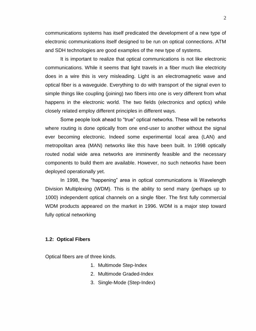
Fig 1.1: Three different kinds of optical fiber
The difference between them is in the way light travels along the fiber. The
top section of the figure shows the operation of “multimode” fiber. There are two
different parts to the fiber. In the figure, there is a core of 50 microns (µ m) in
diameter and a cladding of 125 µ m in diameter. (Fiber size is normally quoted as
the core diameter followed by the cladding diameter. Thus the fiber in the figure
is identified as 50/125.) The cladding surrounds the core. The cladding glass has
a different (lower) refractive index than that of the core, and the boundary forms a
mirror.
Light is transmitted (with very low loss) down the fiber by reflection from
the mirror boundary between the core and the cladding. This phenomenon is
called “total internal reflection”. Perhaps the most important characteristic is that
the fiber will bend around corners to a radius of only a few centimetres without
any loss of the light.
4
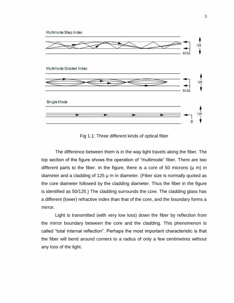
Multimode Step-Index Fiber
Fig 1.2: Multimode Step-Index Fiber
Fiber that has a core diameter large enough for the light used to find
multiple paths is called “multimode” fiber. For a fiber with a core diameter of 62.5
microns using light of wavelength 1300 nm, the number of modes is around 400
depending on the difference in refractive index between the core and the
cladding.
The problem with multimode operation is that some of the paths taken by
particular modes are longer than other paths. This means that light will arrive at
different times according to the path taken. Therefore the pulse tends to disperse
(spread out) as it travels through the fiber. This effect is one cause of
“intersymbol interference”. This restricts the distance that a pulse can be usefully
sent over multimode fiber.
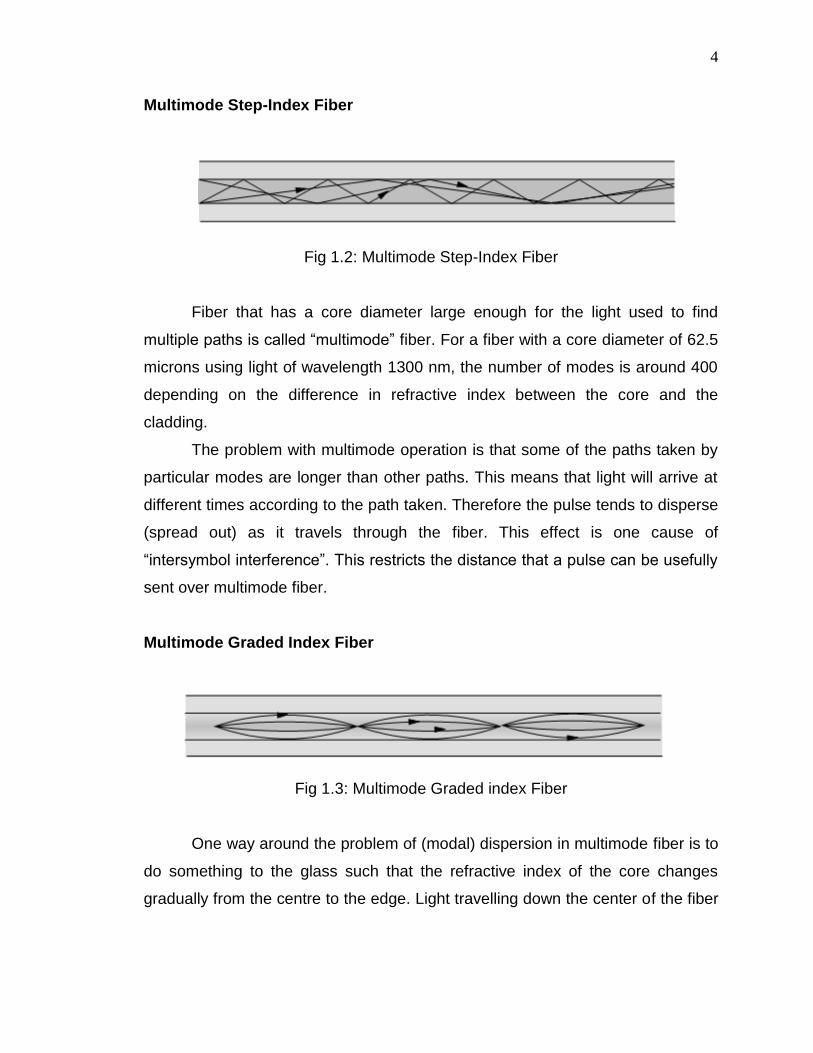
Multimode Graded Index Fiber
Fig 1.3: Multimode Graded index Fiber
One way around the problem of (modal) dispersion in multimode fiber is to
do something to the glass such that the refractive index of the core changes
gradually from the centre to the edge. Light travelling down the center of the fiber
5
experiences a higher refractive index than light that travels further out towards
the cladding. Thus light on the physically shorter paths (modes) travels more
slowly than light on physically longer paths. The light follows a curved trajectory
within the fiber as illustrated in the figure. The aim of this is to keep the speed of
propagation of light on each path the same with respect to the axis of the fiber.
Thus a pulse of light composed of many modes stays together as it travels
through the fiber. This allows transmission for longer distances than does regular
multimode transmission. This type of fiber is called “Graded Index” fiber. Within a
GI fiber light typically travels in around 400 modes (at a wavelength of 1300 nm)
or 800 modes (in the 800 nm band).
Note that only the refractive index of the core is graded. There is still a
cladding of lower refractive index than the outer part of the core.
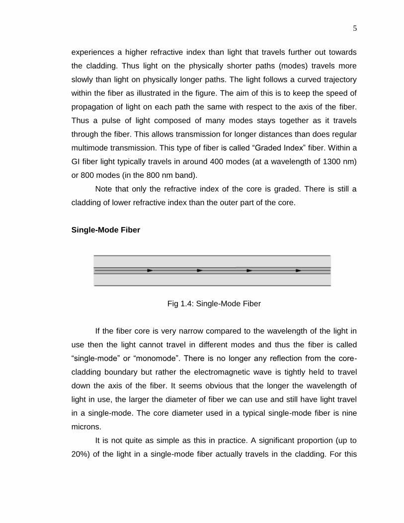
Single-Mode Fiber
Fig 1.4: Single-Mode Fiber
If the fiber core is very narrow compared to the wavelength of the light in
use then the light cannot travel in different modes and thus the fiber is called
“single-mode” or “monomode”. There is no longer any reflection from the core-
cladding boundary but rather the electromagnetic wave is tightly held to travel
down the axis of the fiber. It seems obvious that the longer the wavelength of
light in use, the larger the diameter of fiber we can use and still have light travel
in a single-mode. The core diameter used in a typical single-mode fiber is nine
microns.
It is not quite as simple as this in practice. A significant proportion (up to
20%) of the light in a single-mode fiber actually travels in the cladding. For this
6
reason the “apparent diameter” of the core (the region in which most of the light
travels) is somewhat wider than the core itself. The region in which light travels in
a single-mode fiber is often called the “mode field” and the mode field diameter is
quoted instead of the core diameter. The mode field varies in diameter
depending on the relative refractive indices of core and cladding,
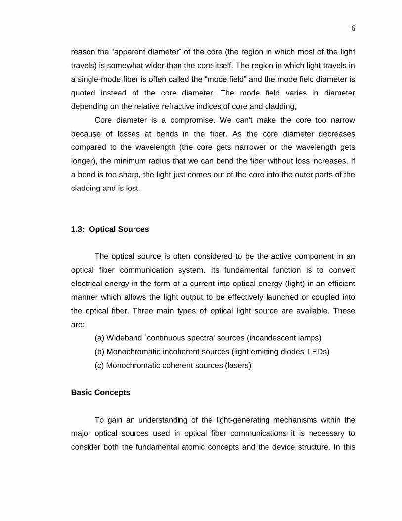
Core diameter is a compromise. We can't make the core too narrow
because of losses at bends in the fiber. As the core diameter decreases
compared to the wavelength (the core gets narrower or the wavelength gets
longer), the minimum radius that we can bend the fiber without loss increases. If
a bend is too sharp, the light just comes out of the core into the outer parts of the
cladding and is lost.
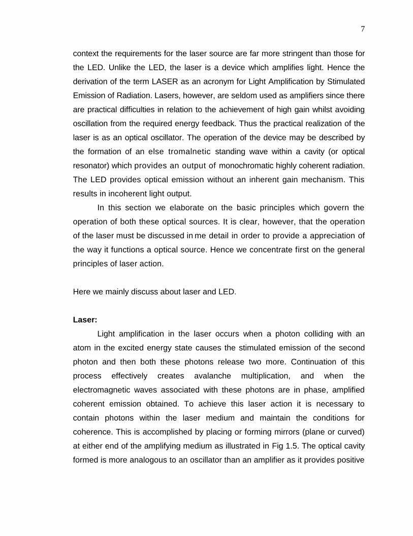
1.3: Optical Sources
The optical source is often considered to be the active component in an
optical fiber communication system. Its fundamental function is to convert
electrical energy in the form of a current into optical energy (light) in an efficient
manner which allows the light output to be effectively launched or coupled into
the optical fiber. Three main types of optical light source are available. These
are:
(a) Wideband `continuous spectra' sources (incandescent lamps)
(b) Monochromatic incoherent sources (light emitting diodes' LEDs)
(c) Monochromatic coherent sources (lasers)
Basic Concepts
To gain an understanding of the light-generating mechanisms within the
major optical sources used in optical fiber communications it is necessary to
consider both the fundamental atomic concepts and the device structure. In this
7
context the requirements for the laser source are far more stringent than those for
the LED. Unlike the LED, the laser is a device which amplifies light. Hence the
derivation of the term LASER as an acronym for Light Amplification by Stimulated
Emission of Radiation. Lasers, however, are seldom used as amplifiers since there
are practical difficulties in relation to the achievement of high gain whilst avoiding
oscillation from the required energy feedback. Thus the practical realization of the
laser is as an optical oscillator. The operation of the device may be described by
the formation of an else tromalnetic standing wave within a cavity (or optical
resonator) which provides an output of monochromatic highly coherent radiation.
The LED provides optical emission without an inherent gain mechanism. This
results in incoherent light output.
In this section we elaborate on the basic principles which govern the
operation of both these optical sources. It is clear, however, that the operation
of the laser must be discussed in me detail in order to provide a appreciation of
the way it functions a optical source. Hence we concentrate first on the general
principles of laser action.
Here we mainly discuss about laser and LED.
Laser:
Light amplification in the laser occurs when a photon colliding with an
atom in the excited energy state causes the stimulated emission of the second
photon and then both these photons release two more. Continuation of this
process effectively creates avalanche multiplication, and when the
electromagnetic waves associated with these photons are in phase, amplified
coherent emission obtained. To achieve this laser action it is necessary to
contain photons within the laser medium and maintain the conditions for
coherence. This is accomplished by placing or forming mirrors (plane or curved)
at either end of the amplifying medium as illustrated in Fig 1.5. The optical cavity
formed is more analogous to an oscillator than an amplifier as it provides positive
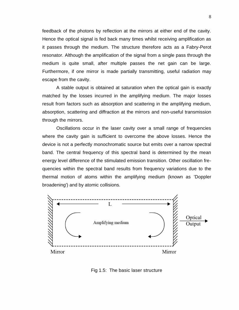
8
feedback of the photons by reflection at the mirrors at either end of the cavity.
Hence the optical signal is fed back many times whilst receiving amplification as
it passes through the medium. The structure therefore acts as a Fabry-Perot
resonator. Although the amplification of the signal from a single pass through the
medium is quite small, after multiple passes the net gain can be large.
Furthermore, if one mirror is made partially transmitting, useful radiation may
escape from the cavity.
A stable output is obtained at saturation when the optical gain is exactly
matched by the losses incurred in the amplifying medium. The major losses
result from factors such as absorption and scattering in the amplifying medium,
absorption, scattering and diffraction at the mirrors and non-useful transmission
through the mirrors.
Oscillations occur in the laser cavity over a small range of frequencies
where the cavity gain is sufficient to overcome the above losses. Hence the
device is not a perfectly monochromatic source but emits over a narrow spectral
band. The central frequency of this spectral band is determined by the mean
energy level difference of the stimulated emission transition. Other oscillation fre-
quencies within the spectral band results from frequency variations due to the
thermal motion of atoms within the amplifying medium (known as „Doppler
broadening') and by atomic collisions.
Fig 1.5: The basic laser structure
9
LED:
Spontaneous emission of radiation in the visible and infrared regions of
the spectrum from a forward biased p-n junction. The normally empty
conduction band of the semiconductor is populated by electrons injected into it
by the forward current through the junction, and light is generated when these
electrons recombine with holes in the valence band to emit a photon. This is the
mechanism by which light is emitted from an LED, but stimulated emission is
not encouraged as it is in the injection laser by the addition of an optical cavity
and mirror facets to provide feedback of photons.
The LED can therefore operate at lower current densities than the
injection laser, but the emitted photons have random phases and the device is
incoherent optical source. Also the energy of the emitted photons is only
roughly equal to the bandgap energy of the semiconductor material, which
gives a much wider spectral linewidth (possibly by a factor of 100) than the
injection laser. The linewidth for an LED is typically 1-2 KT, where K is
Boltzmann's constant and T is the absolute temperature. This gives linewidths
of 30-40 nm at room temperature. Thus the LED supports many optical modes
within its structure and is generally a multimode source which may only be
usefully utilized with multimode step index or graded index fiber.
At present LEDs have several further drawbacks in comparison with
injection lasers. These include:
(a) generally lower optical power coupled into a fiber (mic,owatts);
(b) relatively small modulation bandwidth (often less than 50 MHz);
(c) harmonic distortion.
However, although these problems may initially appear to make the LED
a far less attractive optical source than the injection laser, the device has e
number of distinct advantages which have given it a prominent place in optical
fiber communications:
10
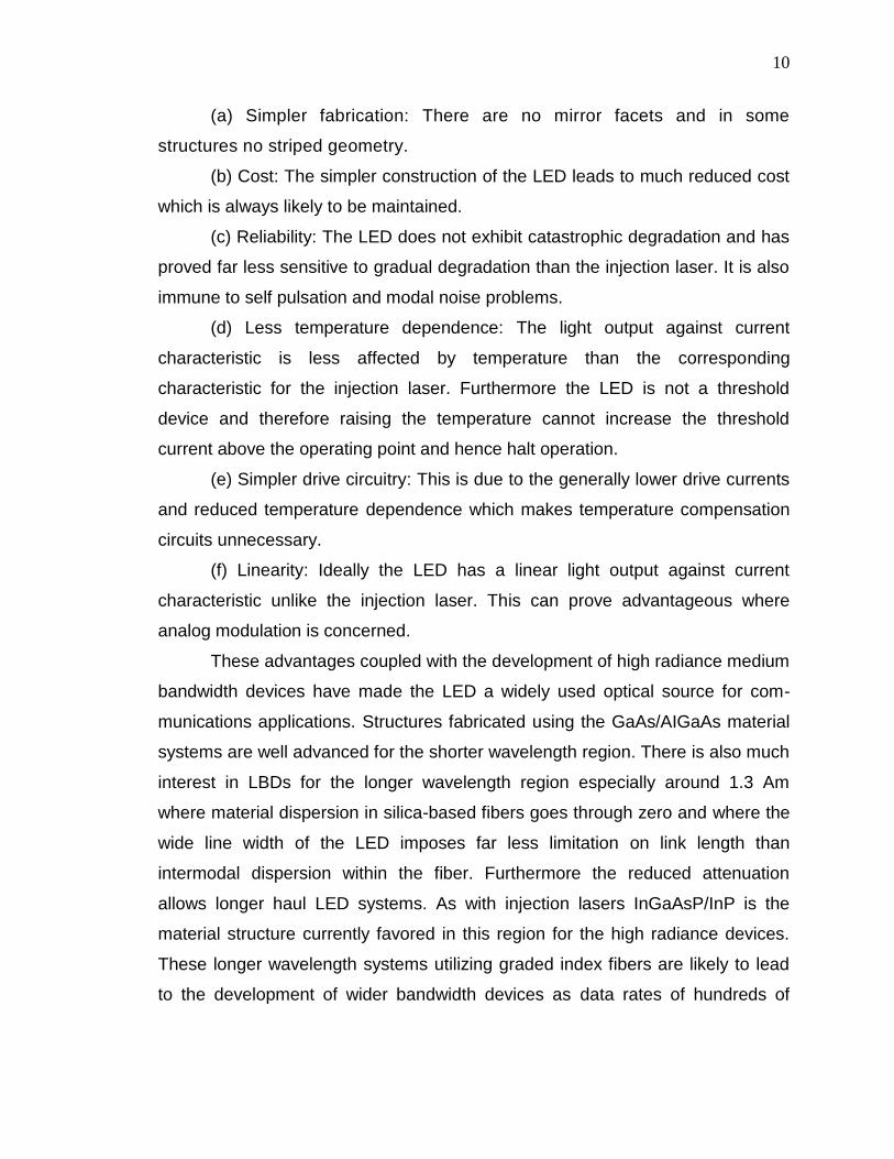
(a) Simpler fabrication: There are no mirror facets and in some
structures no striped geometry.
(b) Cost: The simpler construction of the LED leads to much reduced cost
which is always likely to be maintained.
(c) Reliability: The LED does not exhibit catastrophic degradation and has
proved far less sensitive to gradual degradation than the injection laser. It is also
immune to self pulsation and modal noise problems.
(d) Less temperature dependence: The light output against current
characteristic is less affected by temperature than the corresponding
characteristic for the injection laser. Furthermore the LED is not a threshold
device and therefore raising the temperature cannot increase the threshold
current above the operating point and hence halt operation.
(e) Simpler drive circuitry: This is due to the generally lower drive currents
and reduced temperature dependence which makes temperature compensation
circuits unnecessary.
(f) Linearity: Ideally the LED has a linear light output against current
characteristic unlike the injection laser. This can prove advantageous where
analog modulation is concerned.
These advantages coupled with the development of high radiance medium
bandwidth devices have made the LED a widely used optical source for com-
munications applications. Structures fabricated using the GaAs/AIGaAs material
systems are well advanced for the shorter wavelength region. There is also much
interest in LBDs for the longer wavelength region especially around 1.3 Am
where material dispersion in silica-based fibers goes through zero and where the
wide line width of the LED imposes far less limitation on link length than
intermodal dispersion within the fiber. Furthermore the reduced attenuation
allows longer haul LED systems. As with injection lasers InGaAsP/InP is the
material structure currently favored in this region for the high radiance devices.
These longer wavelength systems utilizing graded index fibers are likely to lead
to the development of wider bandwidth devices as data rates of hundreds of
11
Mbits-1 are already feasible. It is therefore likely that in the near future injection
lasers will only find major use as single mode devices within single mode fiber
systems for the very long-haul, ultra-wide band applications whilst LEDs will
become the primary source for all other system applications.
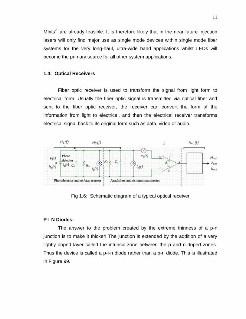
1.4: Optical Receivers
Fiber optic receiver is used to transform the signal from light form to
electrical form. Usually the fiber optic signal is transmitted via optical fiber and
sent to the fiber optic receiver, the receiver can convert the form of the
information from light to electrical, and then the electrical receiver transforms
electrical signal back to its original form such as data, video or audio.
Fig 1.6: Schematic diagram of a typical optical receiver
P-I-N Diodes:
The answer to the problem created by the extreme thinness of a p-n
junction is to make it thicker! The junction is extended by the addition of a very
lightly doped layer called the intrinsic zone between the p and n doped zones.
Thus the device is called a p-i-n diode rather than a p-n diode. This is illustrated
in Figure 99.
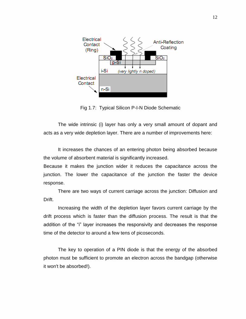
12
Fig 1.7: Typical Silicon P-I-N Diode Schematic
The wide intrinsic (i) layer has only a very small amount of dopant and
acts as a very wide depletion layer. There are a number of improvements here:
It increases the chances of an entering photon being absorbed because
the volume of absorbent material is significantly increased.
Because it makes the junction wider it reduces the capacitance across the
junction. The lower the capacitance of the junction the faster the device
response.
There are two ways of current carriage across the junction: Diffusion and
Drift.
Increasing the width of the depletion layer favors current carriage by the
drift process which is faster than the diffusion process. The result is that the
addition of the “i” layer increases the responsivity and decreases the response
time of the detector to around a few tens of picoseconds.
The key to operation of a PIN diode is that the energy of the absorbed
photon must be sufficient to promote an electron across the bandgap (otherwise
it won't be absorbed!).

13
However, the material will absorb photons of any energy higher than its
bandgap energy. Thus when discussing PIN diodes it is common to talk about
the “cutoff wavelength”. Typically PIN diodes will operate at any wavelength
shorter than the cutoff wavelength. This suggests the idea of using a material
with a low bandgap energy for all PIN diodes regardless of the wavelength.
Unfortunately, the lower the bandgap energy the higher the “dark current”
(thermal noise). Indeed but for this characteristic germanium would be the
material of choice for all PIN diodes! It is low in cost and has two useful
bandgaps (an indirect bandgap at 0.67 eV and a direct bandgap at 0.81 eV).
However it has a relatively high dark current compared to other materials.
This means that the materials used for PIN diode construction are different
depending on the band of wavelengths for which it is to be used. However, this
restriction is nowhere near as stringent as it is for lasers and LEDs where the
characteristics of the material restrict the device to a very narrow range. The
optimal way is to choose a material with a bandgap energy slightly lower than the
energy of the longest wavelength you want to detect.
An interesting consequence to note here is that these crystalline
semiconductor materials are transparent at wavelengths longer than their cutoff.
Thus, if we could “see” with 1500 nm eyes a crystal of pure silicon (which
appears dark grey in visible light) would look like a piece of quartz or diamond.
Typical materials used in the three communication wavelength “windows” are as
follows:
500-1000 nm Band
Silicon PIN diodes operate over a range of 500 to 1120 nm as silicon has
a bandgap energy of 1.11 eV. Since silicon technology is very low cost silicon is
the material of choice in this band.
However, silicon is an indirect bandgap material (at the wavelengths we
are interested in) and this makes it relatively inefficient. (Silicon PIN diodes are
14
not as sensitive as PIN diodes made from other materials in this band.) This is
the same characteristic that prevents the use of silicon for practical lasers.
1300 nm (1250 nm to 1400 nm) Band
In this band indium gallium arsenide phosphide (InGaAsP) and
germanium can be used. Germanium has a lower bandgap energy (0.67 eV
versus 0.89 eV for InGaAsP) and hence it can theoretically be used at longer
wavelengths. However, other effects in Ge limit it to wavelengths below 1400 nm.
InGaAsP is significantly more expensive than Ge but it is also significantly more
efficient (devices are more sensitive).
1550 nm Band (1500 nm to 1600 nm)
The material used here is usually InGaAs (indium gallium arsenide).
InGaAs has a bandgap energy of 0.77 eV.
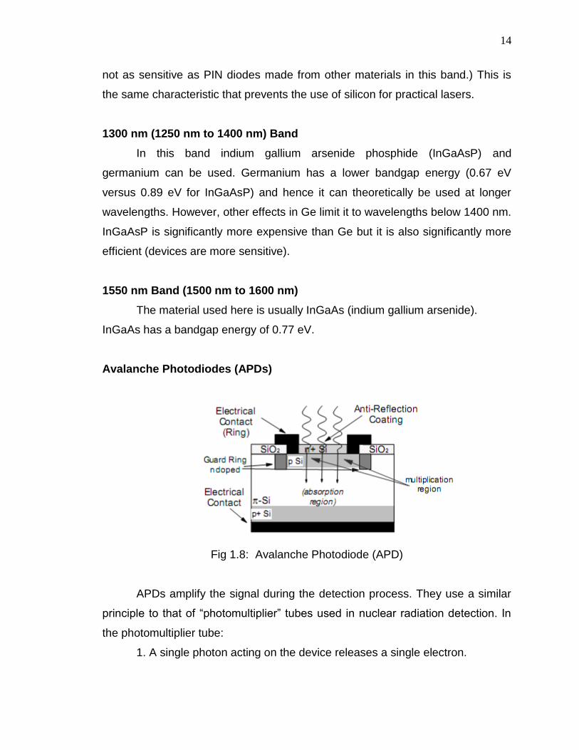
Avalanche Photodiodes (APDs)
Fig 1.8: Avalanche Photodiode (APD)
APDs amplify the signal during the detection process. They use a similar
principle to that of “photomultiplier” tubes used in nuclear radiation detection. In
the photomultiplier tube:
1. A single photon acting on the device releases a single electron.
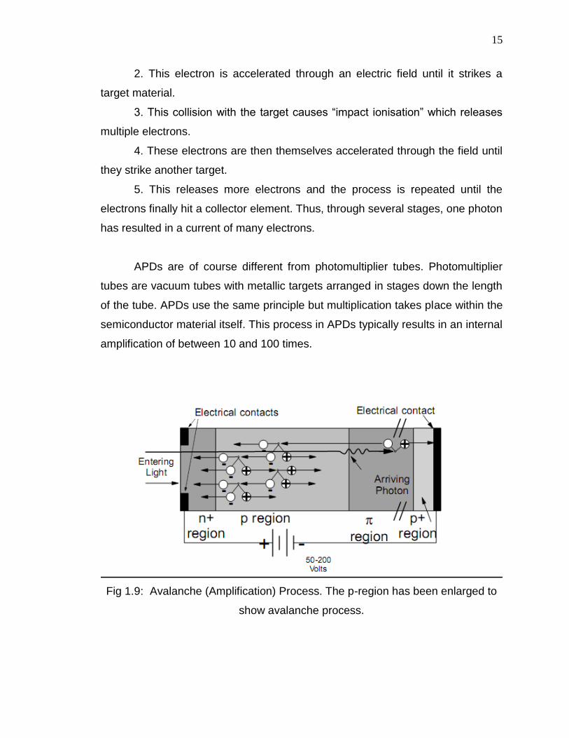
15
2. This electron is accelerated through an electric field until it strikes a
target material.
3. This collision with the target causes “impact ionisation” which releases
multiple electrons.
4. These electrons are then themselves accelerated through the field until
they strike another target.
5. This releases more electrons and the process is repeated until the
electrons finally hit a collector element. Thus, through several stages, one photon
has resulted in a current of many electrons.
APDs are of course different from photomultiplier tubes. Photomultiplier
tubes are vacuum tubes with metallic targets arranged in stages down the length
of the tube. APDs use the same principle but multiplication takes place within the
semiconductor material itself. This process in APDs typically results in an internal
amplification of between 10 and 100 times.
Fig 1.9: Avalanche (Amplification) Process. The p-region has been enlarged to
show avalanche process.
16
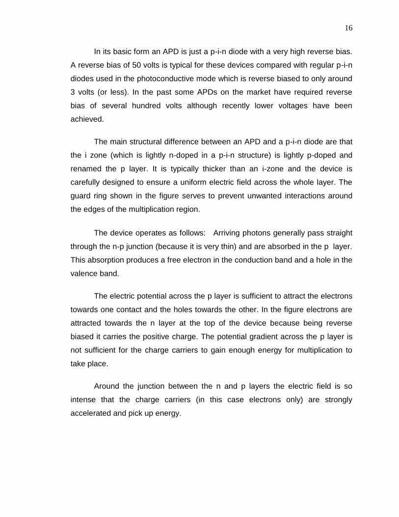
In its basic form an APD is just a p-i-n diode with a very high reverse bias.
A reverse bias of 50 volts is typical for these devices compared with regular p-i-n
diodes used in the photoconductive mode which is reverse biased to only around
3 volts (or less). In the past some APDs on the market have required reverse
bias of several hundred volts although recently lower voltages have been
achieved.
The main structural difference between an APD and a p-i-n diode are that
the i zone (which is lightly n-doped in a p-i-n structure) is lightly p-doped and
renamed the p layer. It is typically thicker than an i-zone and the device is
carefully designed to ensure a uniform electric field across the whole layer. The
guard ring shown in the figure serves to prevent unwanted interactions around
the edges of the multiplication region.
The device operates as follows: Arriving photons generally pass straight
through the n-p junction (because it is very thin) and are absorbed in the p layer.
This absorption produces a free electron in the conduction band and a hole in the
valence band.
The electric potential across the p layer is sufficient to attract the electrons
towards one contact and the holes towards the other. In the figure electrons are
attracted towards the n layer at the top of the device because being reverse
biased it carries the positive charge. The potential gradient across the p layer is
not sufficient for the charge carriers to gain enough energy for multiplication to
take place.
Around the junction between the n and p layers the electric field is so
intense that the charge carriers (in this case electrons only) are strongly
accelerated and pick up energy.

17
When these electrons (now moving with a high energy) collide with other
atoms in the lattice they produce new electron-hole pairs. This process is called
“impact ionisation”.
The newly released charge carriers (both electrons and holes) are
themselves accelerated (in opposite directions) and may collide again.
APD Characteristics
The most important characteristics of APDs are their sensitivity, their
operating speed, their gain-bandwidth product and the level of noise.
Sensitivity of APDs
The extreme sensitivity of APDs is the major reason for using them.
Operating Speed
The same factors (such as device capacitance) that limit the speed of p-i-
n diodes also influence APDs. However, with APDs there is another factor:
“Avalanche Buildup Time”. Because (as discussed above) both carriers can
create ionisation an avalanche can last quite a long time. This is caused by the to
and fro movement of electrons and holes as ionisations occur. Provided the
propensity for ionisation in the minority carrier is relatively low, the avalanche will
slow and stop but this takes some time.
Avalanche Buildup Time thus limits the maximum speed of the APD.
Gain-Bandwidth Product
The accepted measure of “goodness” of a photodetector is the gain-
bandwidth product. This is usually expressed as a gain figure in dB multiplied by
the detector bandwidth (the fastest speed that can be detected) in GHz. A very
good current APD might have a gain-bandwidth product of 150 GHz.
18
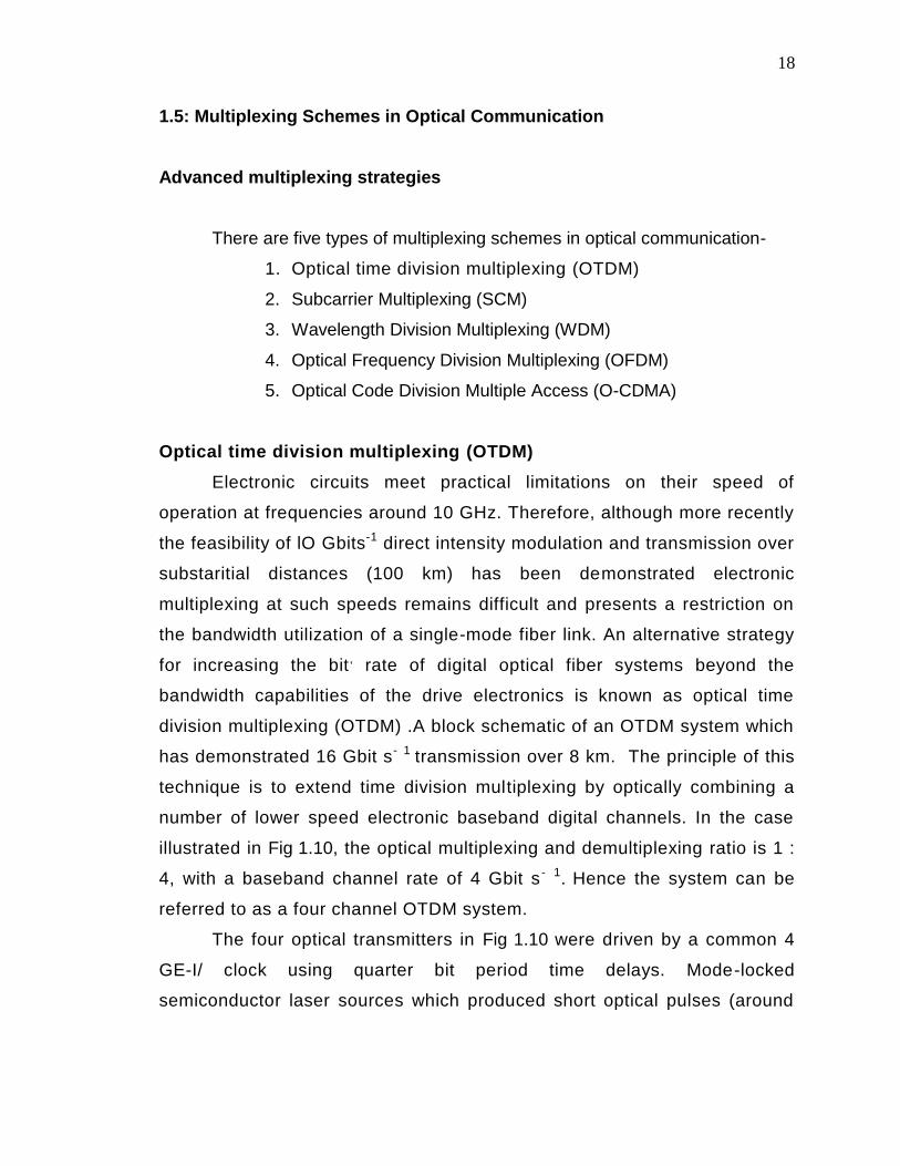
1.5: Multiplexing Schemes in Optical Communication
Advanced multiplexing strategies
There are five types of multiplexing schemes in optical communication-
1. Optical time division multiplexing (OTDM)
2. Subcarrier Multiplexing (SCM)
3. Wavelength Division Multiplexing (WDM)
4. Optical Frequency Division Multiplexing (OFDM)
5. Optical Code Division Multiple Access (O-CDMA)
Optical time division multiplexing (OTDM)
Electronic circuits meet practical limitations on their speed of
operation at frequencies around 10 GHz. Therefore, although more recently
the feasibility of lO Gbits-1 direct intensity modulation and transmission over
substaritial distances (100 km) has been demonstrated electronic
multiplexing at such speeds remains difficult and presents a restriction on
the bandwidth utilization of a single-mode fiber link. An alternative strategy
for increasing the bit, rate of digital optical fiber systems beyond the
bandwidth capabilities of the drive electronics is known as optical time
division multiplexing (OTDM) .A block schematic of an OTDM system which
has demonstrated 16 Gbit s- 1 transmission over 8 km. The principle of this
technique is to extend time division multiplexing by optically combining a
number of lower speed electronic baseband digital channels. In the case
illustrated in Fig 1.10, the optical multiplexing and demultiplexing ratio is 1 :
4, with a baseband channel rate of 4 Gbit s - 1. Hence the system can be
referred to as a four channel OTDM system.
The four optical transmitters in Fig 1.10 were driven by a common 4
GE-I/ clock using quarter bit period time delays. Mode-locked
semiconductor laser sources which produced short optical pulses (around
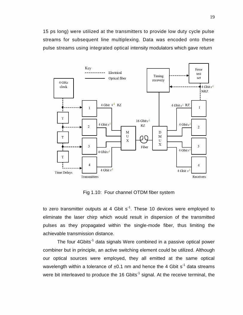
19
15 ps long) were utilized at the transmitters to provide low duty cycle pulse
streams for subsequent line multiplexing. Data was encoded onto these
pulse streams using integrated optical intensity modulators which gave return
Fig 1.10: Four channel OTDM fiber system
to zero transmitter outputs at 4 Gbit s-1. These 10 devices were employed to
eliminate the laser chirp which would result in dispersion of the transmitted
pulses as they propagated within the single-mode fiber, thus limiting the
achievable transmission distance.
The four 4Gbits-1 data signals Were combined in a passive optical power
combiner but in principle, an active switching element could be utilized. Although
our optical sources were employed, they all emitted at the same optical
wavelength within a tolerance of ±0.1 nm and hence the 4 Gbit s-1 data streams
were bit interleaved to produce the 16 Gbits-1 signal. At the receive terminal, the
20
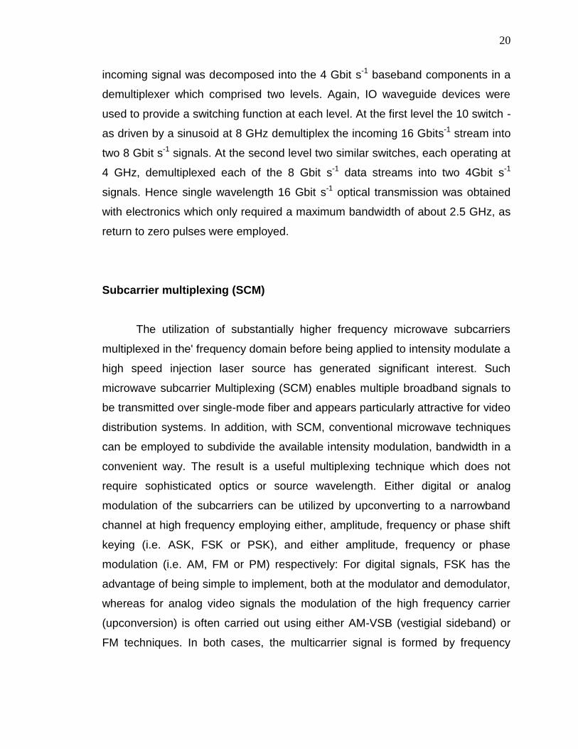
incoming signal was decomposed into the 4 Gbit s-1 baseband components in a
demultiplexer which comprised two levels. Again, IO waveguide devices were
used to provide a switching function at each level. At the first level the 10 switch -
as driven by a sinusoid at 8 GHz demultiplex the incoming 16 Gbits-1 stream into
two 8 Gbit s-1 signals. At the second level two similar switches, each operating at
4 GHz, demultiplexed each of the 8 Gbit s-1 data streams into two 4Gbit s-1
signals. Hence single wavelength 16 Gbit s-1 optical transmission was obtained
with electronics which only required a maximum bandwidth of about 2.5 GHz, as
return to zero pulses were employed.
Subcarrier multiplexing (SCM)
The utilization of substantially higher frequency microwave subcarriers
multiplexed in the' frequency domain before being applied to intensity modulate a
high speed injection laser source has generated significant interest. Such
microwave subcarrier Multiplexing (SCM) enables multiple broadband signals to
be transmitted over single-mode fiber and appears particularly attractive for video
distribution systems. In addition, with SCM, conventional microwave techniques
can be employed to subdivide the available intensity modulation, bandwidth in a
convenient way. The result is a useful multiplexing technique which does not
require sophisticated optics or source wavelength. Either digital or analog
modulation of the subcarriers can be utilized by upconverting to a narrowband
channel at high frequency employing either, amplitude, frequency or phase shift
keying (i.e. ASK, FSK or PSK), and either amplitude, frequency or phase
modulation (i.e. AM, FM or PM) respectively: For digital signals, FSK has the
advantage of being simple to implement, both at the modulator and demodulator,
whereas for analog video signals the modulation of the high frequency carrier
(upconversion) is often carried out using either AM-VSB (vestigial sideband) or
FM techniques. In both cases, the multicarrier signal is formed by frequency
21
division multiplexing (FDM) of the modulated microwave subcarriers in the
electrical domain prior to conversion to an 'intensity modulated optical signal.
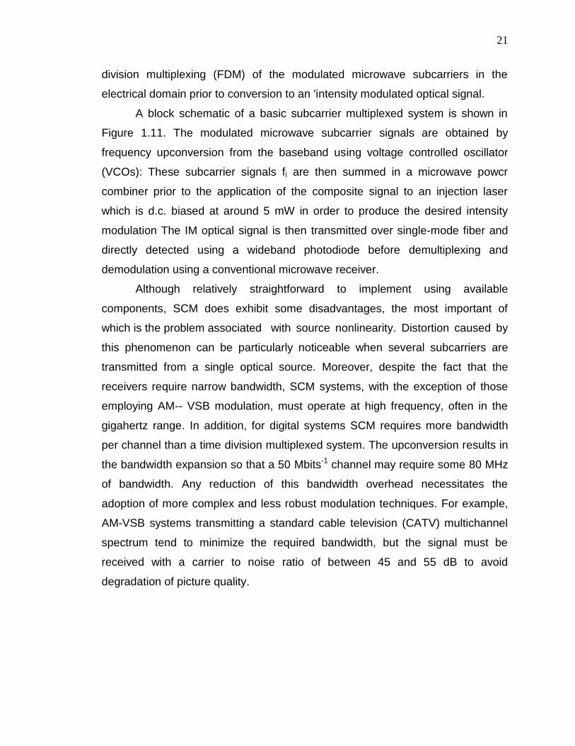
A block schematic of a basic subcarrier multiplexed system is shown in
Figure 1.11. The modulated microwave subcarrier signals are obtained by
frequency upconversion from the baseband using voltage controlled oscillator
(VCOs): These subcarrier signals fi are then summed in a microwave powcr
combiner prior to the application of the composite signal to an injection laser
which is d.c. biased at around 5 mW in order to produce the desired intensity
modulation The IM optical signal is then transmitted over single-mode fiber and
directly detected using a wideband photodiode before demultiplexing and
demodulation using a conventional microwave receiver.
Although relatively straightforward to implement using available
components, SCM does exhibit some disadvantages, the most important of
which is the problem associated with source nonlinearity. Distortion caused by
this phenomenon can be particularly noticeable when several subcarriers are
transmitted from a single optical source. Moreover, despite the fact that the
receivers require narrow bandwidth, SCM systems, with the exception of those
employing AM-- VSB modulation, must operate at high frequency, often in the
gigahertz range. In addition, for digital systems SCM requires more bandwidth
per channel than a time division multiplexed system. The upconversion results in
the bandwidth expansion so that a 50 Mbits-1 channel may require some 80 MHz
of bandwidth. Any reduction of this bandwidth overhead necessitates the
adoption of more complex and less robust modulation techniques. For example,
AM-VSB systems transmitting a standard cable television (CATV) multichannel
spectrum tend to minimize the required bandwidth, but the signal must be
received with a carrier to noise ratio of between 45 and 55 dB to avoid
degradation of picture quality.
22
Fig 1.11: Basic subcarrier multiplexed (SCM) fiber system
The transmission of multiple CATV channels over substantial
unrepeatered distances with good quality reception has, however, been
demonstrated with SCM using frequency modulation (i.e. FM-FDM). For
example, thirty-four multiple sub-nyquist-sampling encoding (MUSE) high
definition television (HDTV) channels, each requiring an FM bandwidth of 27
23
MHz, have been transmitted over an unrepeatered distance of 42 km. This
transmission system, which operated at a wavelength of 1.3 pm, provided a
carrier to noise ratio of 17.5 dB at the receive terminal. Furthermore, an
unrepeatered transmission distance in excess of 100 km has also been
demonstrated with SCM when operating at a wavelength of 1.54 m. In this case,
some eight baseband video channels, each of which was frequency modulated to
occupy around 30 MHz of bandwidth, were then frequency multiplexed over a
range 840 to 1160 MHz before directly modulating a distributed feedback laser.
Apart from the possibility of combining digital and analog subcarrier
multiplexed signals into a composite -signal, an alternative attractive strategy is
the so-called hybrid SCM system which combines a baseband digital signal with
a high frequency composite microwave signal. In this case the receiver shown in
Figure 1.11 cannot 6e narrowband but must have a bandwidth from d.c. to
beyond the highest microwave signal frequency employed. As mentioned
previously, SCM is under investigation for application in video distribution
systems and networks. In such systems only a single channel needs to be
selected for demodulation. Hence a tunable local oscillator, mixer and narrow
band filter can be utilized at the receive terminals (Figure 1.11) to simultaneously
select the desired SCM channel and downconvert it to a more convenient
intermediate frequency (IF) signal. Finally, the lF signal can be input to an
appropriate demodulator to recover the baseband video signal.
Wavelength division multiplexing
Wavelength division multiplexing (WDM) involves the transmission of a
number al different peak wavelength optical signals in parallel on a single optical
fiber. Although in spectral terms optical WDM is analogous to electrical frequency
division multiplexing, it has the distinction that each WDM channel effectively has
access to the entire intensity modulation fiber bandwidth which with current
24
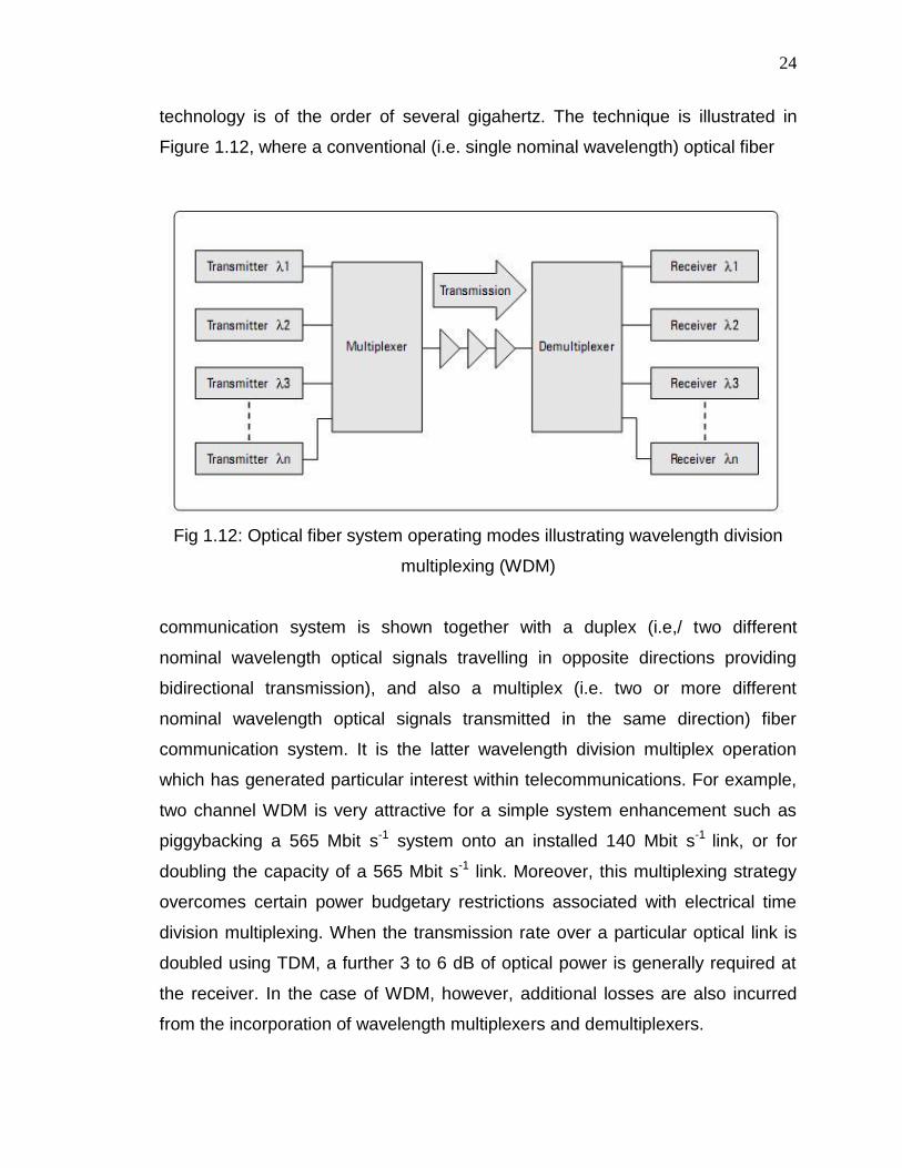
technology is of the order of several gigahertz. The technique is illustrated in
Figure 1.12, where a conventional (i.e. single nominal wavelength) optical fiber
Fig 1.12: Optical fiber system operating modes illustrating wavelength division
multiplexing (WDM)
communication system is shown together with a duplex (i.e,/ two different
nominal wavelength optical signals travelling in opposite directions providing
bidirectional transmission), and also a multiplex (i.e. two or more different
nominal wavelength optical signals transmitted in the same direction) fiber
communication system. It is the latter wavelength division multiplex operation
which has generated particular interest within telecommunications. For example,
two channel WDM is very attractive for a simple system enhancement such as
piggybacking a 565 Mbit s-1 system onto an installed 140 Mbit s-1 link, or for
doubling the capacity of a 565 Mbit s-1 link. Moreover, this multiplexing strategy
overcomes certain power budgetary restrictions associated with electrical time
division multiplexing. When the transmission rate over a particular optical link is
doubled using TDM, a further 3 to 6 dB of optical power is generally required at
the receiver. In the case of WDM, however, additional losses are also incurred
from the incorporation of wavelength multiplexers and demultiplexers.
25
Wavelength division multiplexing in IM/DD optical fiber systems can be
implemented using either LED or injection laser sources with either multimode or
single-mode fiber. More recently, however, the wide scale deployment of single-
mode fiber has encouraged the investigation of WDM on this transmission
medium. In particular, the potential utilization of the separate wavelength
channels to provide dedicated communication services to individual subscriber
terminals is an attractive concept within telecommunications. For example, a
multiwavelength, single-mode optical 'star network called LAMBDANET has been
developed using commercial components. This network, which is internally
nonblocking, has been configured to allow the integration of point-to-point and
point-to-rnultipoint wideband services, including video distribution applications.
The LAMBDANET star network incorporates a sixteen port passive
transmission star coupler. Each node was equipped with a single distributed
feedback laser selected with centre wavelengths spaced at 2 nm intervals over
the range 1527 to 1561 nm. Hence each node transmitted at a unique
wavelength, providing a contention-free broadcast capability to all other nodes.
At the receive terminals every node could detect transmissions from all other
nodes using a wavelength demultiplexer and sixteen optical receivers. Moreover,
the wavelength channels on the network were-demonstrated to operate at a
transmission rate of 2 Gbit s-1 over a distance of 40 km.
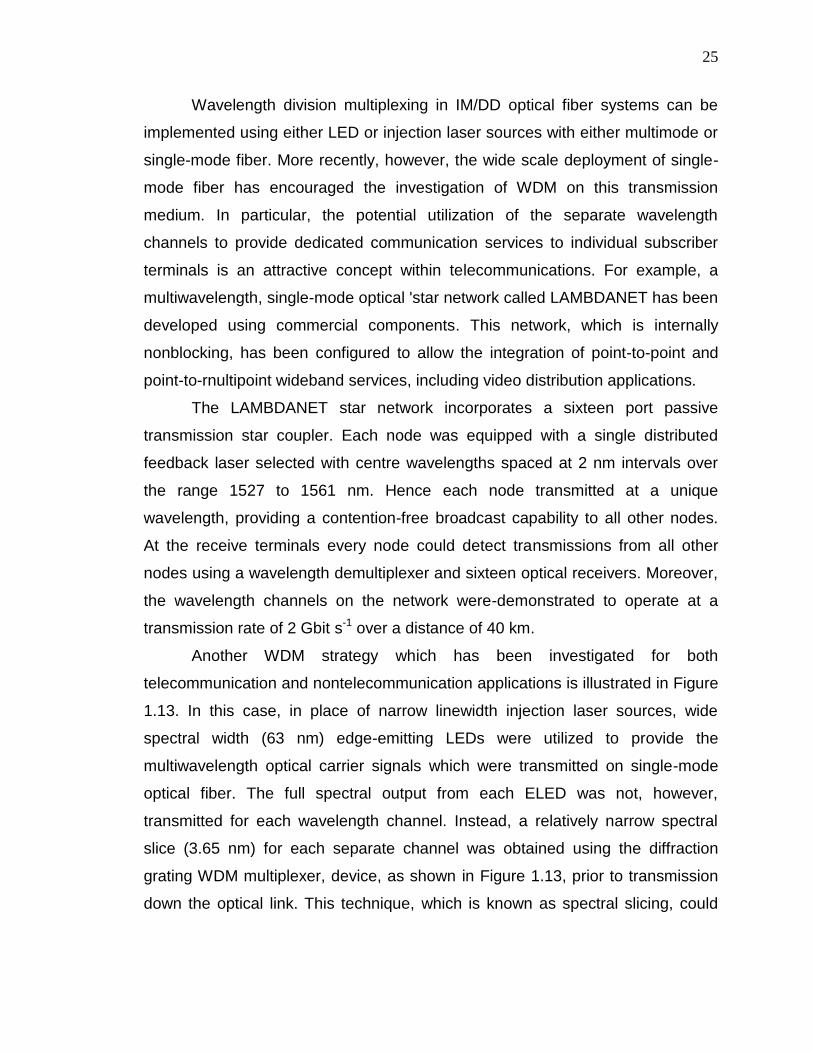
Another WDM strategy which has been investigated for both
telecommunication and nontelecommunication applications is illustrated in Figure
1.13. In this case, in place of narrow linewidth injection laser sources, wide
spectral width (63 nm) edge-emitting LEDs were utilized to provide the
multiwavelength optical carrier signals which were transmitted on single-mode
optical fiber. The full spectral output from each ELED was not, however,
transmitted for each wavelength channel. Instead, a relatively narrow spectral
slice (3.65 nm) for each separate channel was obtained using the diffraction
grating WDM multiplexer, device, as shown in Figure 1.13, prior to transmission
down the optical link. This technique, which is known as spectral slicing, could
26
enable LEDs with the same overall spectral output to be employed whilst still
providing the distinctive wavelength channels for transmission between each
subscriber terminal. In this case a WDM dernultiplexer device is located at a
distribution point in order to separate and distribute the different wavelength
optical channels to the appropriate subscriber receive terminals.
Fig 1.13: Spectral slicing of LED outputs to form several WDM channels
A similar strategy has been demonstrated for sixteen channels using
superluminescent LEDs, again transmitting on single-mode fiber [Ref. 94].
Moreover, the technique has also been employed in nontelecommunication
areas to provide multiple wavelength channels from single LED sources, usually
on multimode fiber, in order to, for example, service a multiple optical sensor
system in which each wavelength channel supplies a signal to a different optical
sensor device.
27
1.6: Optical amplifier
An optical amplifier is a device that amplifies an optical signal directly,
without the need to first convert it to an electrical signal. An optical amplifier may
be thought of as without an optical cavity or one in which feedback from the
cavity is suppressed. Stimulated emission in the amplifiers gain medium causes
amplification of incoming light. Optical amplifiers are important in optical
communication. There are many types of Amplifiers in optical communication
system. But Erbium-doped fiber amplifier (EDFA) familiar in DWDM.
1.7: Objectives of the project
To analyze the performance of a Wavelength Division Multiplexing (WDM)
transmission system with Optical Amplifiers in Cascade considering the effect of
accumulated Amplifier‟s Spontaneous Emission (ASE) noise. To find the
expression for signal to ASE noise ratio and to include to crosstalk due WDM
Multiplexers/ Demultiplexers at each WDM node. And to determine the
performance results in terms of signal to ASE noise ratio and signal to Crosstalk
ratio and the system Bit Error Rate (BER) at a given bit rate.
28
CHAPTER II
WDM SYSTEM
In fiber-optic communications, wavelength-division multiplexing (WDM) is
a technology which multiplexes multiple optical carrier signals on a single optical
fiber by using different wavelengths (colours) of laser light to carry different
signals. This allows for a multiplication in capacity, in addition to enabling
bidirectional communications over one strand of fiber. This is a form of frequency
division multiplexing (FDM) but is commonly called wavelength division
multiplexing.
The term wavelength-division multiplexing is commonly applied to an
optical carrier (which is typically described by its wavelength), whereas
frequency-division multiplexing typically applies to a radio carrier (which is more
often described by frequency). However, since wavelength and frequency are
inversely proportional, and since radio and light are both forms of
electromagnetic radiation, the two terms are equivalent in this context.
A WDM system uses a multiplexer at the transmitter to join the signals
together and a demultiplexer at the receiver to split them apart. With the right
type of fiber it is possible to have a device that does both simultaneously, and
can function as an optical add-drop multiplexer. The optical filtering devices used
have traditionally been etalons, stable solid-state single-frequency Fabry-Perot
interferometers in the form of thin-film-coated optical glass.
The concept was first published in 1970, and by 1978 WDM systems were
being realized in the laboratory. The first WDM systems only combined two
signals. Modern systems can handle up to 160 signals and can thus expand a
basic 10 Gbit/s fiber system to a theoretical total capacity of over 1.6 Tbit/s over
a single fiber pair.
29
WDM systems are popular with telecommunications companies because
they allow them to expand the capacity of the network without laying more fiber.
WDM systems are divided in different wavelength patterns, conventional
or coarse and dense WDM. Conventional WDM systems provide up to 16
channels in the 3rd transmission window (C-band) of silica fibers around 1550
nm. DWDM uses the same transmission window but with denser channel
spacing.
Dense WDM:
Dense Wavelength Division Multiplexing, or DWDM for short, refers
originally to optical signals multiplexed within the 1550-nm band so as to
leverage the capabilities (and cost) of erbium doped fiber amplifiers (EDFAs),
which are effective for wavelengths between approximately 1525-1565 nm (C
band), or 1570-1610 nm (L band). EDFAs were originally developed to replace
SONET/SDH optical-electrical-optical (OEO) regenerators, which they have
made practically obsolete. EDFAs can amplify any optical signal in their
operating range, regardless of the modulated bit rate. In terms of multi-
wavelength signals, so long as the EDFA has enough pump energy available to
it, it can amplify as many optical signals as can be multiplexed into its
amplification band (though signal densities are limited by choice of modulation
format). EDFAs therefore allow a single-channel optical link to be upgraded in bit
rate by replacing only equipment at the ends of the link, while retaining the
existing EDFA or series of EDFAs through a long haul route. Furthermore, single-
wavelength links using EDFAs can similarly be upgraded to WDM links at
reasonable cost. The EDFAs cost is thus leveraged across as many channels as
can be multiplexed into the 1550-nm band.
30
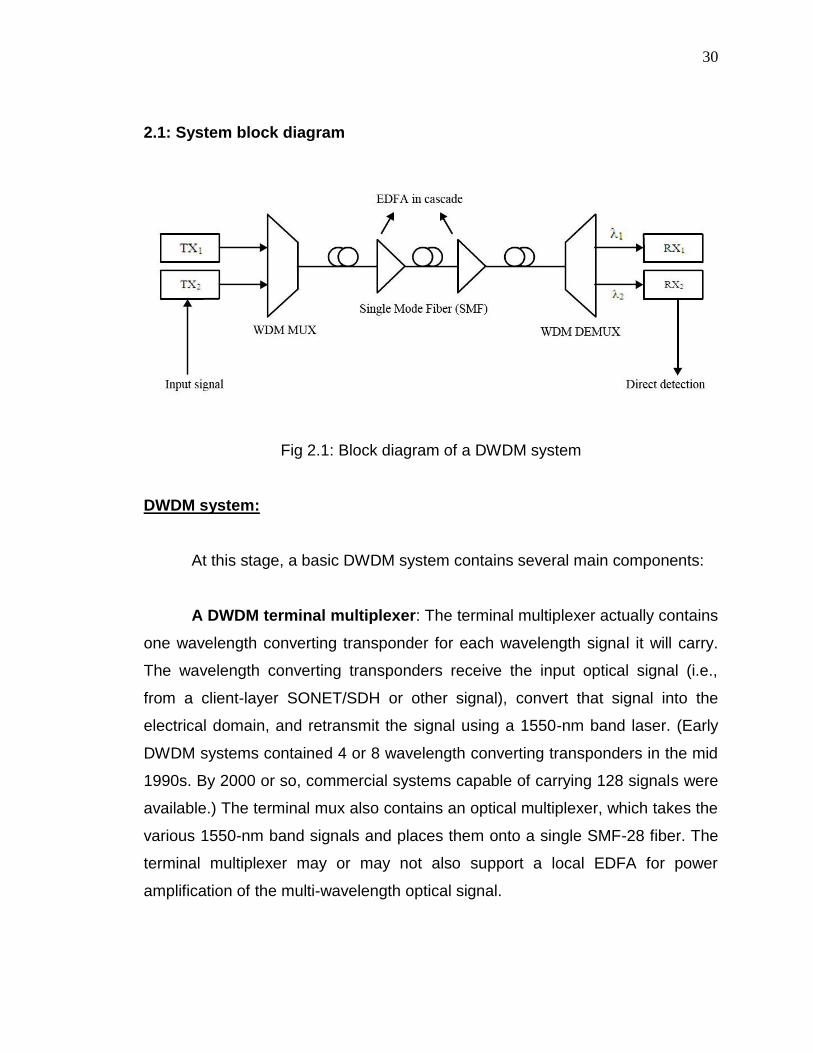
2.1: System block diagram
Fig 2.1: Block diagram of a DWDM system
DWDM system:
At this stage, a basic DWDM system contains several main components:
A DWDM terminal multiplexer: The terminal multiplexer actually contains
one wavelength converting transponder for each wavelength signal it will carry.
The wavelength converting transponders receive the input optical signal (i.e.,
from a client-layer SONET/SDH or other signal), convert that signal into the
electrical domain, and retransmit the signal using a 1550-nm band laser. (Early
DWDM systems contained 4 or 8 wavelength converting transponders in the mid
1990s. By 2000 or so, commercial systems capable of carrying 128 signals were
available.) The terminal mux also contains an optical multiplexer, which takes the
various 1550-nm band signals and places them onto a single SMF-28 fiber. The
terminal multiplexer may or may not also support a local EDFA for power
amplification of the multi-wavelength optical signal.
31
An intermediate optical terminal or Optical Add-drop multiplexer:
This is a remote amplification site that amplifies the multi-wavelength signal that
may have traversed up to 140 km or more before reaching the remote site.
Optical diagnostics and telemetry are often extracted or inserted at such a site, to
allow for localization of any fiber breaks or signal impairments. In more
sophisticated systems (which are no longer point-to-point), several signals out of
the multiwavelength signal may be removed and dropped locally.
A DWDM terminal demultiplexer. The terminal demultiplexer breaks the
multi-wavelength signal back into individual signals and outputs them on
separate fibers for client-layer systems (such as SONET/SDH) to detect.
Originally, this demultiplexing was performed entirely passively, except for some
telemetry, as most SONET systems can receive 1550-nm signals. However, in
order to allow for transmission to remote client-layer systems (and to allow for
digital domain signal integrity determination) such demultiplexed signals are
usually sent to O/E/O output transponders prior to being relayed to their client-
layer systems. Often, the functionality of output transponder has been integrated
into that of input transponder, so that most commercial systems have
transponders that support bi-directional interfaces on both their 1550-nm (i.e.,
internal) side, and external (i.e., client-facing) side. Transponders in some
systems supporting 40 GHz nominal operation may also perform forward error
correction (FEC) via 'digital wrapper' technology, as described in the ITU-T G.709
standard.
2.2: WDM Multiplexer / Demultiplexer :
Interference-based DMUX/MUX:
Mach-Zehnder Interferometer (MZI)
Multi-layer Thin Film Filter
32
Grating-based DMUX/MUX:
Fiber Bragg Grating (FBG)
Arrayed Waveguide Grating (AWG)
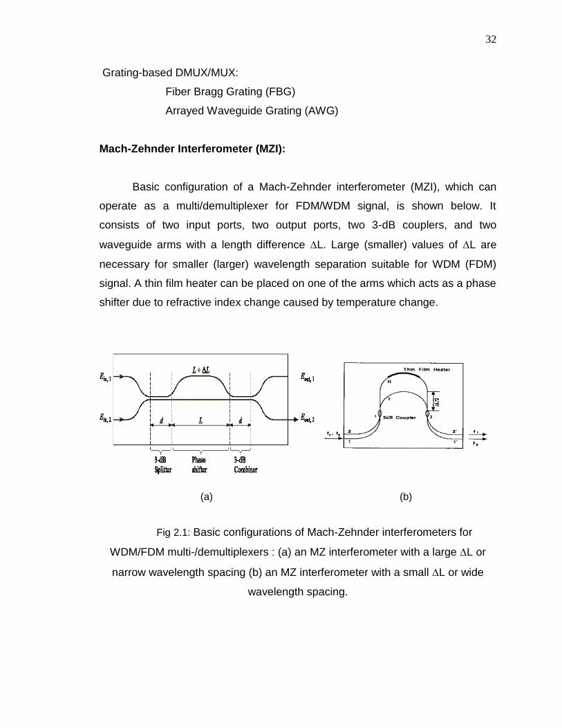
Mach-Zehnder Interferometer (MZI):
Basic configuration of a Mach-Zehnder interferometer (MZI), which can
operate as a multi/demultiplexer for FDM/WDM signal, is shown below. It
consists of two input ports, two output ports, two 3-dB couplers, and two
waveguide arms with a length difference L. Large (smaller) values of L are
necessary for smaller (larger) wavelength separation suitable for WDM (FDM)
signal. A thin film heater can be placed on one of the arms which acts as a phase
shifter due to refractive index change caused by temperature change.
(a) (b)
Fig 2.1: Basic configurations of Mach-Zehnder interferometers for
WDM/FDM multi-/demultiplexers : (a) an MZ interferometer with a large L or
narrow wavelength spacing (b) an MZ interferometer with a small L or wide
wavelength spacing.
33
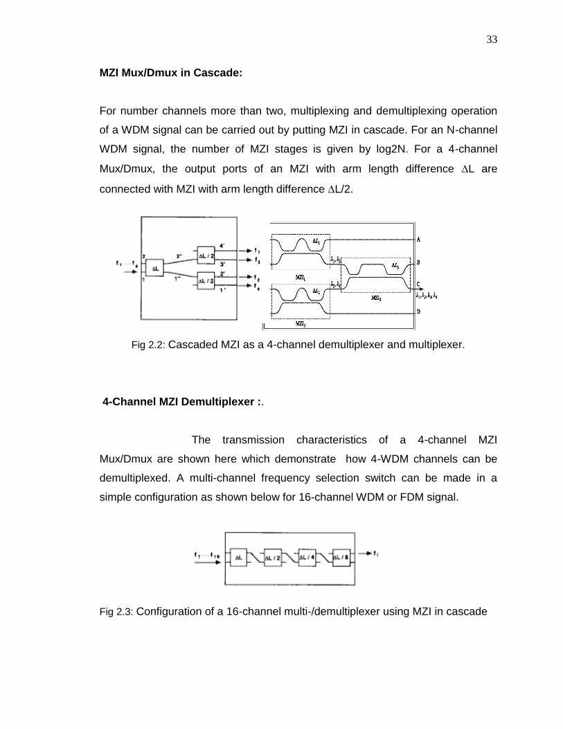
MZI Mux/Dmux in Cascade:
For number channels more than two, multiplexing and demultiplexing operation
of a WDM signal can be carried out by putting MZI in cascade. For an N-channel
WDM signal, the number of MZI stages is given by log2N. For a 4-channel
Mux/Dmux, the output ports of an MZI with arm length difference L are
connected with MZI with arm length difference L/2.
Fig 2.2: Cascaded MZI as a 4-channel demultiplexer and multiplexer.
4-Channel MZI Demultiplexer :.
The transmission characteristics of a 4-channel MZI
Mux/Dmux are shown here which demonstrate how 4-WDM channels can be
demultiplexed. A multi-channel frequency selection switch can be made in a
simple configuration as shown below for 16-channel WDM or FDM signal.
Fig 2.3: Configuration of a 16-channel multi-/demultiplexer using MZI in cascade
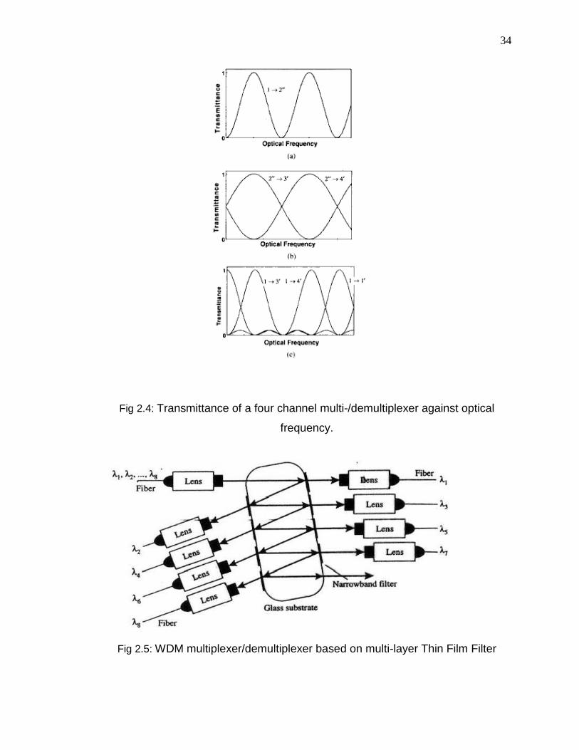
34
Fig 2.4: Transmittance of a four channel multi-/demultiplexer against optical
frequency.
Fig 2.5: WDM multiplexer/demultiplexer based on multi-layer Thin Film Filter
35
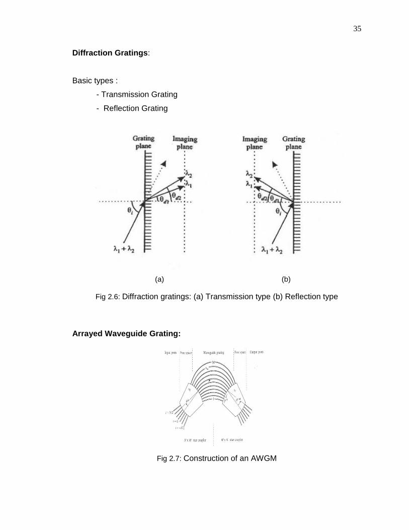
Diffraction Gratings:
Basic types :
- Transmission Grating
- Reflection Grating
(a) (b)
Fig 2.6: Diffraction gratings: (a) Transmission type (b) Reflection type
Arrayed Waveguide Grating:
Fig 2.7: Construction of an AWGM

36
Advantages of AWG:
-Can be effectively used in a dense WDM system to enlarge transmission
capacity
-Improve flexibility as a router in a WDM network
-Flexibility in channel number (N = 400)
-Low crosstalk ( < -30 dB)
-128 x128 AWG with 25 GHz spacing, x-talk < -16 dB
-Low insertion loss ( <3 dB)
Limitations of an AWG:
- Amplitude error
- Phase error
- Crosstalk due to above
Required Characteristic of an AWG for DWDM :
- Flat
- Wideband
Flat characteristic can be achieved by using various methods :
- Y-branch
- Sinc functional field
- MM interference
- Two-focal point method
- Parabolic tapers .
Applications of an AWG:
• Multiplexer/Demultiplexer
• Optical Add-drop multiplexer (OADM)
• Multichannel light source
37
• Wavelength selective switch
• Wavelength router
• Thermo-optic (TO) Tunable Optical filter
AWG in cascade:
The capacity of a dense WDM transmission system can be greatly
increased by using two or multiplexer/demultiplexer in cascade which offers
multi-stage multiplexing demultiplexing facilities. Such arrangements can be
achieved by putting MZI and AWG in cascade. Although there is an increase in
insertion loss, the crosstalk can be reduced significantly.
Advantage of DWDM:
DWDM systems have to maintain more stable wavelength or frequency
than those needed for CWDM because of the closer spacing of the wavelengths.
Precision temperature control of laser transmitter is required in DWDM systems
to prevent "drift" off a very narrow frequency window of the order of a few GHz. In
addition, since DWDM provides greater maximum capacity it tends to be used at
a higher level in the communications hierarchy than CWDM, for example on the
Internet backbone and is therefore associated with higher modulation rates, thus
creating a smaller market for DWDM devices with very high performance levels.
These factors of smaller volume and higher performance result in DWDM
systems typically being more expensive than CWDM.
Recent innovations in DWDM transport systems include pluggable and
software-tunable transceiver modules capable of operating on 40 or 80 channels.
This dramatically reduces the need for discrete spare pluggable modules, when a
handful of pluggable devices can handle the full range of wavelengths.
38
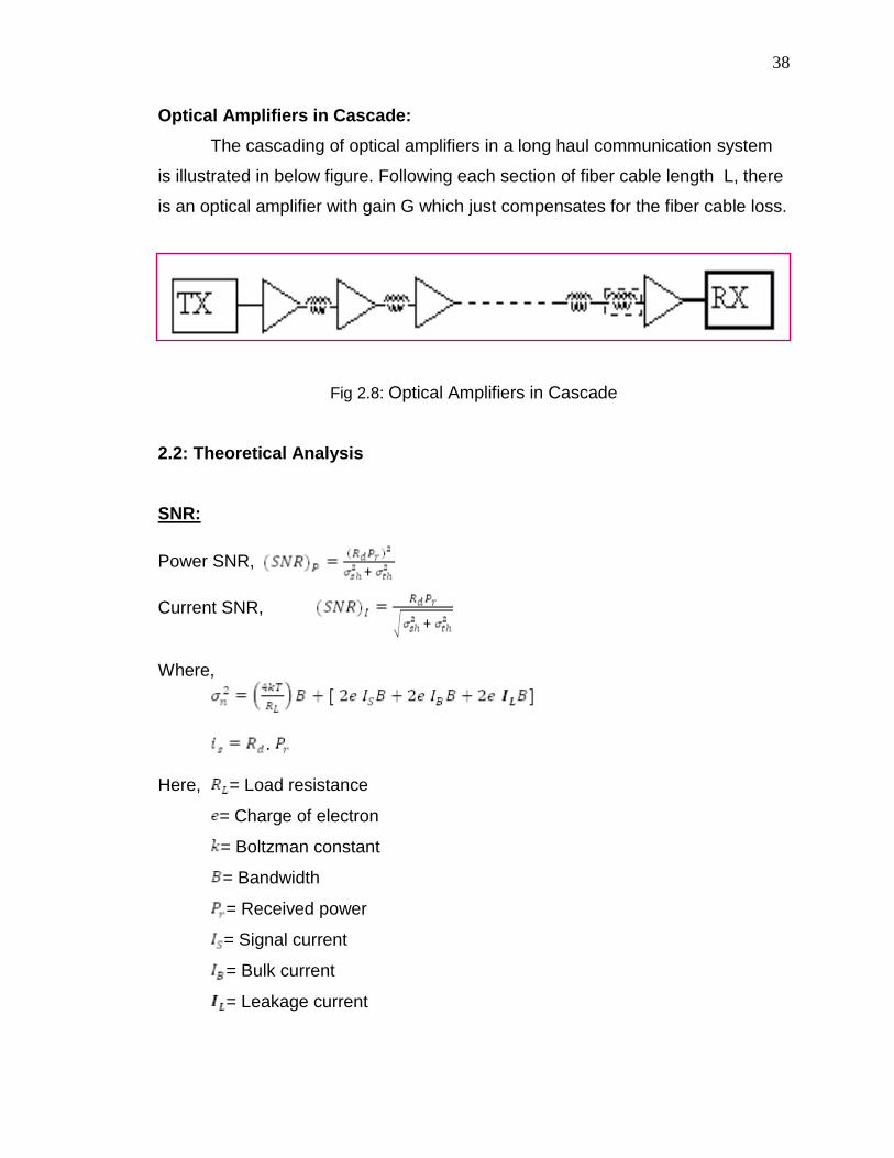
Optical Amplifiers in Cascade:
The cascading of optical amplifiers in a long haul communication system
is illustrated in below figure. Following each section of fiber cable length L, there
is an optical amplifier with gain G which just compensates for the fiber cable loss.
Fig 2.8: Optical Amplifiers in Cascade
2.2: Theoretical Analysis
SNR:
Power SNR,
Current SNR,
Where,
.
Here, = Load resistance
= Charge of electron
= Boltzman constant
= Bandwidth
= Received power
= Signal current
= Bulk current
= Leakage current
39
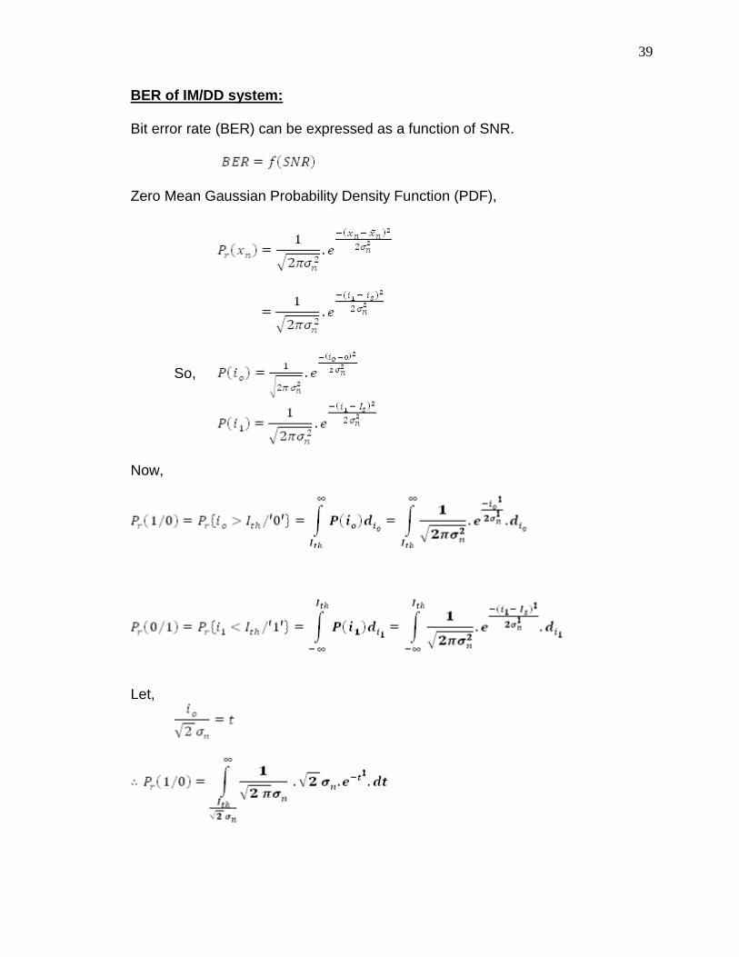
BER of IM/DD system: Bit error rate (BER) can be expressed as a function of SNR.
Zero Mean Gaussian Probability Density Function (PDF),
So,
Now,
Let,
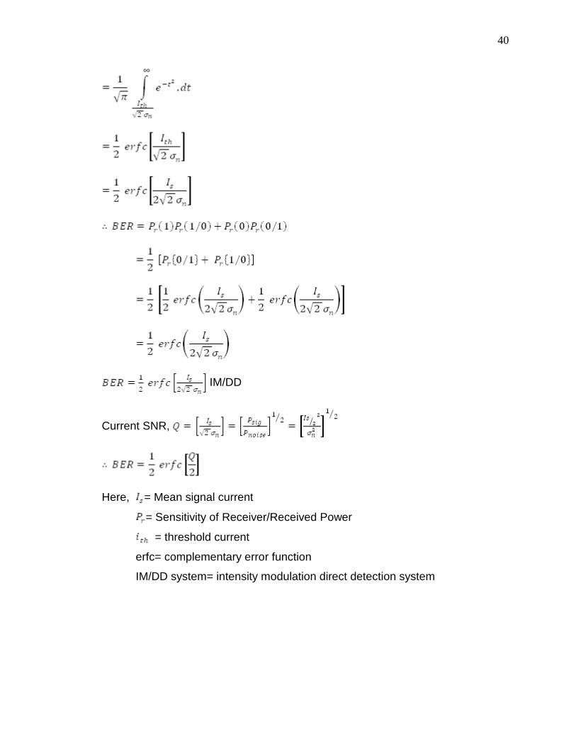
40
IM/DD
Current SNR,
Here, = Mean signal current
= Sensitivity of Receiver/Received Power
= threshold current
erfc= complementary error function
IM/DD system= intensity modulation direct detection system
41
Power Spectral density (PSD) of Spontaneous Emission noise:
Nsp(f) = nsp (G-1) hf = K hf
Where
nsp = spontaneous emission factor
G = amplifier gain
h = Plank's constant
f = frequency of radiation
Let,
Pi = Power output from the Tx = Power input to the fiber
If the amplifier gain is adjusted to compensate for the total losses, then
G (dB) = PL(dB) = (fc + j) L (dB)
G = 10 -[(fc + j) L]/10
The total number of amplifiers = N = Lt/L
Then total Spontaneous emission noise at the input of the receiver
Pase = N K hf B
Where B = Bandwidth of amplifier
The Optical power received by the Receiver = Pr = Pi G
Therefore the Signal to noise ratio at the receiver input,
Amplifier noise figure,
NKhf
P
P
GP
N
SL
i
ase
ijfc 10/
10
out
in
NS
NSF
)/(
)/(
42
Cascaded Optical amplifier system with different gain:
Let,
Gk = Gain of the k-th amplifier
Fk = Noise figure of the k-th amplifier
k = loss coefficient of the k-th fiber section
Then the total system noise figure is given by,
Where
(S/N)T = SNR at the output of the Tx
(S/N)M = SNR at the output of M-th amplifier
If 1G1 =2G2 =…… = kGk =1
Then
M
Tto
NS
NSF
)/(
)/(
1
1
32211
3
211
2
1
1 ......M
kkkM
Mto
G
F
GG
F
G
FFF
1
1
32211
33
2211
22
11
11 ......M
kkkMM
MMto
GG
GF
GGG
GF
GG
GF
G
GFF
M
kkkMMto GFGFGFGFGFF
1332211 ..............
43
CHAPTER III
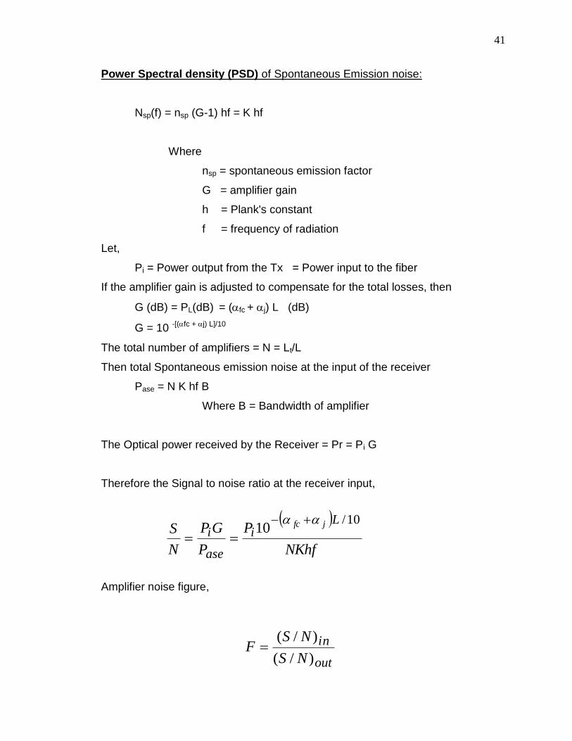
RESULTS AND DISCUSSION Plot 1:
Fig 3.1: SNR (dB) vs Gain (dB)
From the figure, we see that with the increase of gain in the transmission
line, SNR increases. That means the more we use optical amplifiers, the more we get gain, and the more we get SNR which is good.
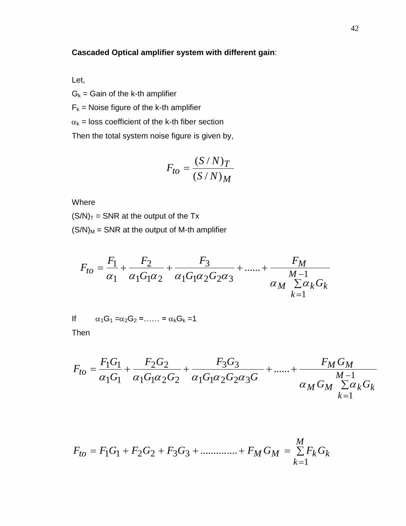
Plot 2:
Fig 3.2: BER vs SNR (dB)
44
The above figure shows us that with the increase of SNR, BER decreases. That means we get more accurate data transmission through optical link. Plot 3:
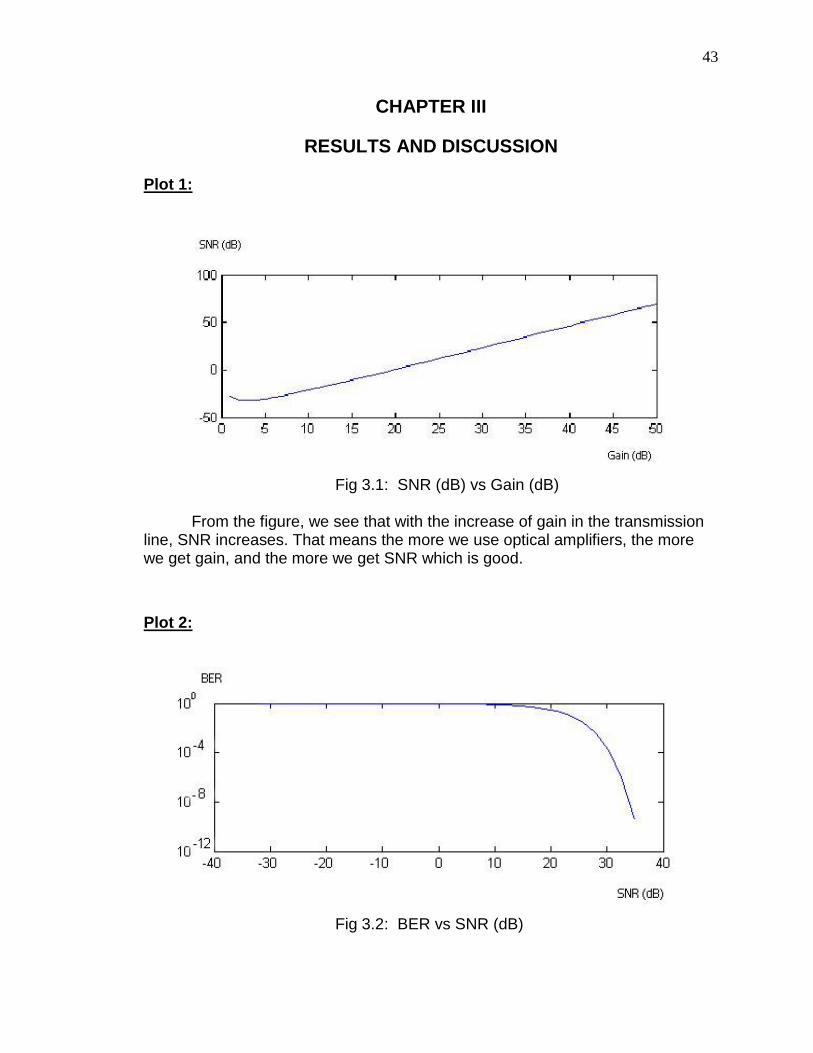
Fig 3.3: BER by Pr (dBm)
From the figure, we see that BER is decreasing with the increase of received power. This figure was plotted for different bit rates. We see from here that as bit rate increases, BER also increases with the increase of received power.
45
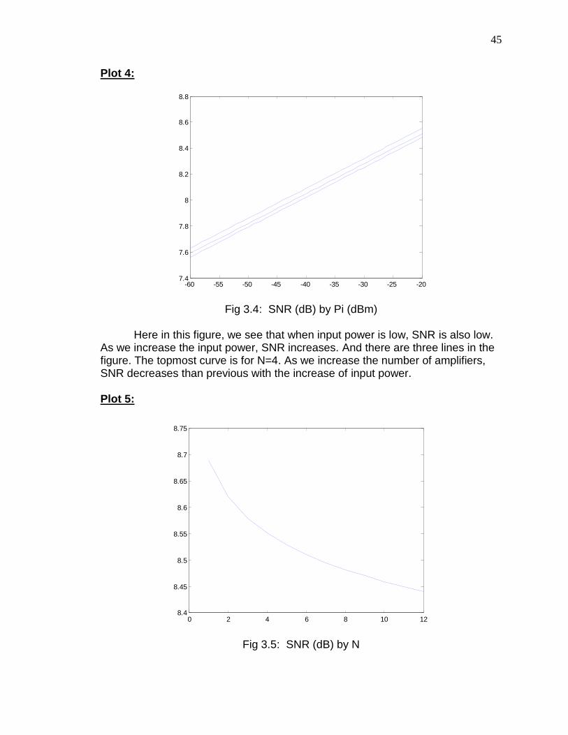
Plot 4:
-60 -55 -50 -45 -40 -35 -30 -25 -207.4
7.6
7.8
8
8.2
8.4
8.6
8.8
Fig 3.4: SNR (dB) by Pi (dBm)
Here in this figure, we see that when input power is low, SNR is also low.
As we increase the input power, SNR increases. And there are three lines in the figure. The topmost curve is for N=4. As we increase the number of amplifiers, SNR decreases than previous with the increase of input power. Plot 5:
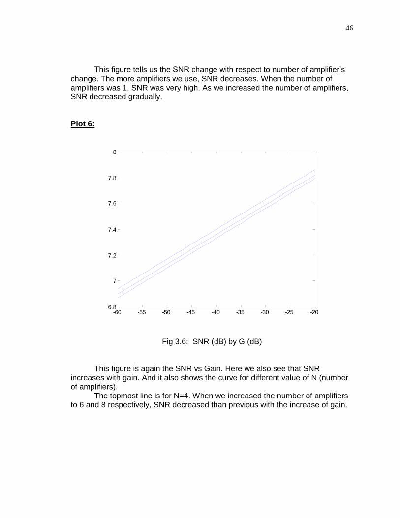
0 2 4 6 8 10 128.4
8.45
8.5
8.55
8.6
8.65
8.7
8.75
Fig 3.5: SNR (dB) by N
46
This figure tells us the SNR change with respect to number of amplifier‟s change. The more amplifiers we use, SNR decreases. When the number of amplifiers was 1, SNR was very high. As we increased the number of amplifiers, SNR decreased gradually. Plot 6:
-60 -55 -50 -45 -40 -35 -30 -25 -206.8
7
7.2
7.4
7.6
7.8
8
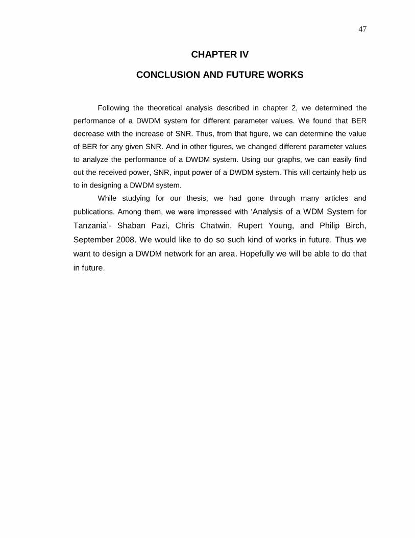
Fig 3.6: SNR (dB) by G (dB)
This figure is again the SNR vs Gain. Here we also see that SNR increases with gain. And it also shows the curve for different value of N (number of amplifiers).
The topmost line is for N=4. When we increased the number of amplifiers to 6 and 8 respectively, SNR decreased than previous with the increase of gain.
47
CHAPTER IV
CONCLUSION AND FUTURE WORKS
Following the theoretical analysis described in chapter 2, we determined the
performance of a DWDM system for different parameter values. We found that BER
decrease with the increase of SNR. Thus, from that figure, we can determine the value
of BER for any given SNR. And in other figures, we changed different parameter values
to analyze the performance of a DWDM system. Using our graphs, we can easily find
out the received power, SNR, input power of a DWDM system. This will certainly help us
to in designing a DWDM system.
While studying for our thesis, we had gone through many articles and
publications. Among them, we were impressed with „Analysis of a WDM System for
Tanzania‟- Shaban Pazi, Chris Chatwin, Rupert Young, and Philip Birch,
September 2008. We would like to do so such kind of works in future. Thus we
want to design a DWDM network for an area. Hopefully we will be able to do that
in future.

48
References:
[1] Optical Fiber Communications Principles and Practice by John M Senior
(2nd Edition)
[2] Understanding Optical Communications by Harry J. R. Dutton (1st Edition
- September 1998)
[3] Fiber-Optic Communications Technology by Djafar K. Mynbaev, Lowell
L. Scheiner
[4] Optical Fiber Communications by Gerd Keiser (2nd Edition)
[5] www.iec.org
[6] www.ieee.org
[7] www.wikipedia.org
[8] www.fiber-optics.info
[9] www.fiber_dispersion.com
[10] Performance Limitations of WDM Optical Transmission System Due to
Cross-Phase Modulation in Presence of Chromatic Dispersion by M. A.
Khayer Azad and M. S. Islam, BUET
[11] Analysis of a WDM System for Tanzania Shaban Pazi, Chris Chatwin,
Rupert Young, and Philip Birch, September 2008
[12] Slides and documents provided by Dr. Satya Prasad Majumder.