
DEM-ADS7870 DATA ACQUISITION SYSTEM - Digi-Key Sheets/Texas Instruments PDFs... · The DEM-ADS7870...
13
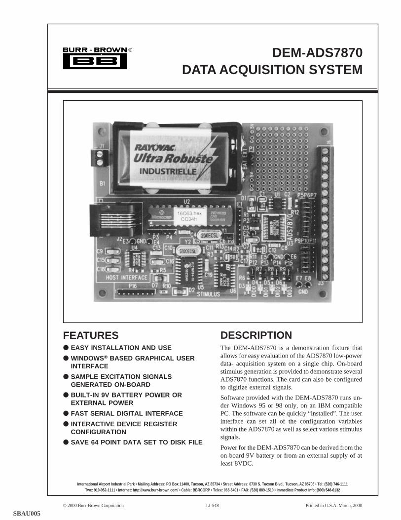
® © 2000 Burr-Brown Corporation LI-548 Printed in U.S.A. March, 2000 DEM-ADS7870 DATA ACQUISITION SYSTEM FEATURES ● EASY INSTALLATION AND USE ● WINDOWS ® BASED GRAPHICAL USER INTERFACE ● SAMPLE EXCITATION SIGNALS GENERATED ON-BOARD ● BUILT-IN 9V BATTERY POWER OR EXTERNAL POWER ● FAST SERIAL DIGITAL INTERFACE ● INTERACTIVE DEVICE REGISTER CONFIGURATION ● SAVE 64 POINT DATA SET TO DISK FILE DESCRIPTION The DEM-ADS7870 is a demonstration fixture that allows for easy evaluation of the ADS7870 low-power data- acquisition system on a single chip. On-board stimulus generation is provided to demonstrate several ADS7870 functions. The card can also be configured to digitize external signals. Software provided with the DEM-ADS7870 runs un- der Windows 95 or 98 only, on an IBM compatible PC. The software can be quickly “installed”. The user interface can set all of the configuration variables within the ADS7870 as well as select various stimulus signals. Power for the DEM-ADS7870 can be derived from the on-board 9V battery or from an external supply of at least 8VDC. International Airport Industrial Park • Mailing Address: PO Box 11400, Tucson, AZ 85734 • Street Address: 6730 S. Tucson Blvd., Tucson, AZ 85706 • Tel: (520) 746-1111 Twx: 910-952-1111 • Internet: http://www.burr-brown.com/ • Cable: BBRCORP • Telex: 066-6491 • FAX: (520) 889-1510 • Immediate Product Info: (800) 548-6132 SBAU005
-
Upload
nguyennhan -
Category
Documents
-
view
216 -
download
1
Transcript of DEM-ADS7870 DATA ACQUISITION SYSTEM - Digi-Key Sheets/Texas Instruments PDFs... · The DEM-ADS7870...
®
© 2000 Burr-Brown Corporation LI-548 Printed in U.S.A. March, 2000
DEM-ADS7870DATA ACQUISITION SYSTEM
FEATURES EASY INSTALLATION AND USE
WINDOWS® BASED GRAPHICAL USERINTERFACE
SAMPLE EXCITATION SIGNALSGENERATED ON-BOARD
BUILT-IN 9V BATTERY POWER OREXTERNAL POWER
FAST SERIAL DIGITAL INTERFACE
INTERACTIVE DEVICE REGISTERCONFIGURATION
SAVE 64 POINT DATA SET TO DISK FILE
DESCRIPTIONThe DEM-ADS7870 is a demonstration fixture thatallows for easy evaluation of the ADS7870 low-powerdata- acquisition system on a single chip. On-boardstimulus generation is provided to demonstrate severalADS7870 functions. The card can also be configuredto digitize external signals.
Software provided with the DEM-ADS7870 runs un-der Windows 95 or 98 only, on an IBM compatiblePC. The software can be quickly “installed”. The userinterface can set all of the configuration variableswithin the ADS7870 as well as select various stimulussignals.
Power for the DEM-ADS7870 can be derived from theon-board 9V battery or from an external supply of atleast 8VDC.
International Airport Industrial Park • Mailing Address: PO Box 11400, Tucson, AZ 85734 • Street Address: 6730 S. Tucson Blvd., Tucson, AZ 85706 • Tel: (520) 746-1111Twx: 910-952-1111 • Internet: http://www.burr-brown.com/ • Cable: BBRCORP • Telex: 066-6491 • FAX: (520) 889-1510 • Immediate P roduct Info: (800) 548-6132
SBAU005
2®
DEM-ADS7870
JUMPER DEFAULT FUNCTION
P1 EXT Power Source
P2 1-2 VREF/BUF_IN Select
P3 Open Configuration U2
P4 Open Configuration U2
P5, P6, P7 5-6 DIO Select
P8 1-2 CCLK Source
P9, P10, P11 9-10 Signal Source
P12 1-2 LED0
P13 1-2 LED1
P14 1-2 LED2
P15 1-2 LED3
P16 Open Stimulus Programming Port
TEST POINT SIGNAL
E1 Interface Logic
E2 VREF Input
E3-E8 Ground Points
TABLE II. Test Point Description.
TABLE I. Configuration Jumpers with Default Factory Settings.
HARDWARE SET-UPThe DEM-ADS7870 uses two embedded “PIC” controllers.The configuration jumpers are set in the manner described inTable I.
An initial demonstration can be run by simply installing a9V battery and moving the P1 jumper to the BAT position.Jumper configurations can be changed later to show otherfeatures.
The test points on the E1 header allow monitoring of the dig-ital interface signals between the DUT and the host controller.
SOFTWARE INSTALLATIONUser-interface software is installed in the normal Windowsmanner. Close all other applications. From the “Start” buttonon the task-bar select “Run”. In the window that opens, type:
d:\ setup
Where: “d” is the letter designation of the CD-ROMdrive on the computer.
Follow the prompts to install the software.
To run the program, left-click on “Start” from the task-barand then expand the “Programs” menu. The applicationprogram is titled “Burr-Brown ADS7870 Application”.
To remove this application, use the Control Panel “Add/Remove software” utility, in the Windows system.
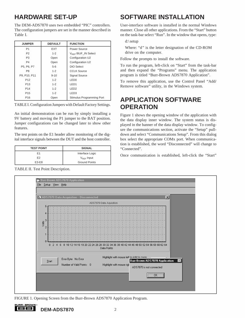
APPLICATION SOFTWAREOPERATIONFigure 1 shows the opening window of the application withthe data display inner window. The system status is dis-played in the banner of the data display window. To config-ure the communications section, activate the “Setup” pull-down and select “Communications Setup”. From this dialogbox select the appropriate COMx port. When communica-tion is established, the word “Disconnected” will change to“Connected”.
Once communication is established, left-click the “Start”
FIGURE 1. Opening Screen from the Burr-Brown ADS7870 Application Program.

3®
DEM-ADS7870
button to get the display as shown in Figure 2. The sine wavegenerator is not synchronized with the conversions of theADS7870, so each data set may start at a different point inthe waveform.
ON-BOARD STIMULUS OPTIONS
FIGURE 2. Typical Data Display with Default Configuration.
From the top menu bar open the “Setup” menu and thenselect “Inputs”. A window, as shown in Figure 3, will bepresented. From this window, it is possible to select thesignal to be digitized and change the relevant register con-tents that configure the ADS7870.
The C-Clock Divisor panel in the lower right hand corner of
FIGURE 3. Setup...Inputs... Screen Start-up Default Values.
the Inputs window must be set to 8 when the device isoperated with the on-board oscillator.
An internally generated signal can be selected from theWaveform pull down menu, as shown in Figure 4.
To digitize a complex waveform, select two sine waves,
FIGURE 4. Waveform Selections.

4®
DEM-ADS7870
setting Freq 1=0.82 and Freq 2 =4.01 for a ratio of 5:1. Theresult is shown in Figure 5.
In Figure 5, there is a box drawn around the waveform. Thisis a zoom window. Place the cursor just to the left of the firstdata point. Holding the left mouse button down, draw a boxas shown. The result of the zoom operation is shown inFigure 6, below.
Acquisition of a DC voltage can also be demonstrated by
A/D conversion should be very close to the first value noted.Reset the Channel Input Configuration to Differential,–LN2+LN3, close the window and collect another data set.The A/D conversion value displayed will be the two’scompliment of the first readings.
To demonstrate the PGA over-range flag, return the configu-ration to the Internal Source stimulus and increase the PGAgain to 20 on the Setup...Inputs control screen. Starting adata collection sequence will result in a display, as shown inFigure 7.
VIEW PULL-DOWN MENU
FIGURE 5. Two Sine Waves.
FIGURE 6. Two Sine Wave Trace After Zoom Operation.
selecting that option from the Internal Stimulus, ...Wave-form menu, and then setting a voltage level by entering avalue between 0 and 16,383. This is useful in demonstratingthe treatment of negative numbers by the ADS7870.
Open the Setup...Inputs screen and set the Waveform DC atsome non-zero value. Execute a data collection sequenceand, using the View Register Values as described below,note the hex code of the last A/D conversion. Through theSetup...Inputs screen, change the stimulus to External Sources,but do not move any jumpers. Select Channel Input Configu-ration to Differential, +LN2–LN3. Close the window andexecute a data collection. The value of the last
FIGURE 7. PGA Overload. Note that the number of valid datapoints will vary depending on the level of the sinewave at the time the data set is collected.
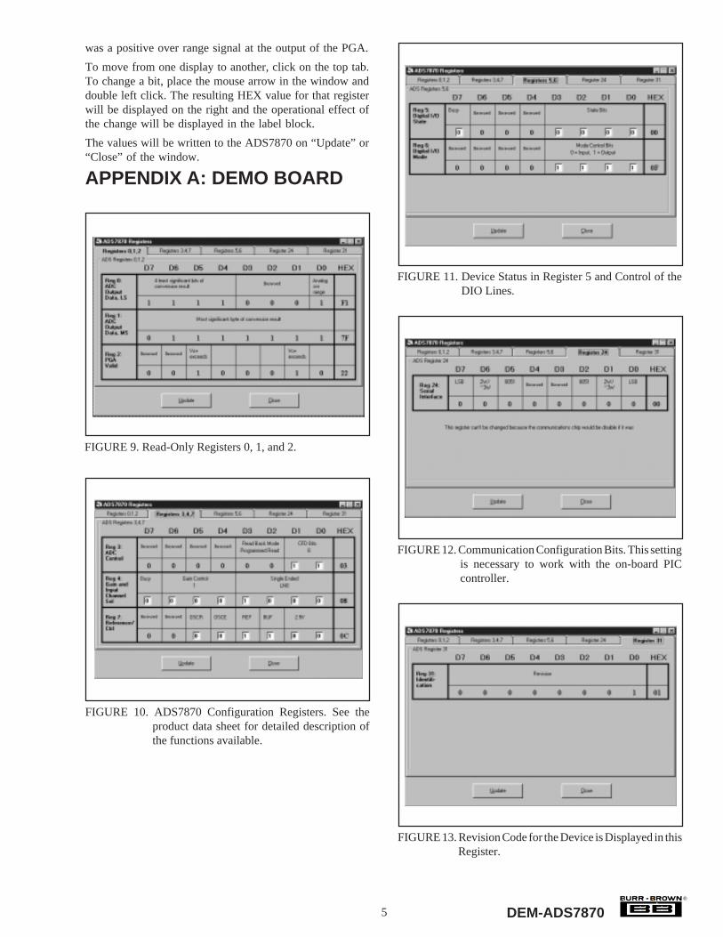
The internal configuration registers of the ADS7870 can beexamined with the View...Register Values, as shown inFigure 8.
The individual bits may be examined and changed where
FIGURE 8. Register Values.
valid, with the pull-down menu View...Register Details.Examples of these screens are given in the following fivefigures.
The contents of register 2 shown in Figure 9 report that there
5®
DEM-ADS7870
was a positive over range signal at the output of the PGA.
To move from one display to another, click on the top tab.To change a bit, place the mouse arrow in the window anddouble left click. The resulting HEX value for that registerwill be displayed on the right and the operational effect ofthe change will be displayed in the label block.
The values will be written to the ADS7870 on “Update” or“Close” of the window.
APPENDIX A: DEMO BOARD
FIGURE 9. Read-Only Registers 0, 1, and 2.
FIGURE 10. ADS7870 Configuration Registers. See theproduct data sheet for detailed description ofthe functions available.
FIGURE 11. Device Status in Register 5 and Control of theDIO Lines.
FIGURE 12. Communication Configuration Bits. This settingis necessary to work with the on-board PICcontroller.
FIGURE 13. Revision Code for the Device is Displayed in thisRegister.

6®
DEM-ADS7870
CONSTRUCTION DETAILSCIRCUIT DIAGRAM AND PC BOARD
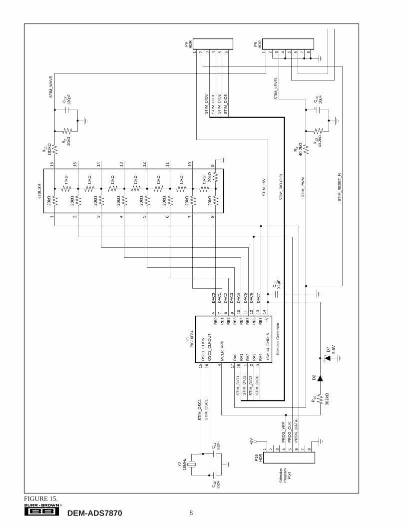
The circuit diagram is presented in three sections. Figure 14 covers the RS232 communications through to the ADS7870.Figure 15 depicts the on-board stimulus generator. Figure 16 shows the interconnect between the sections and the powersupply.
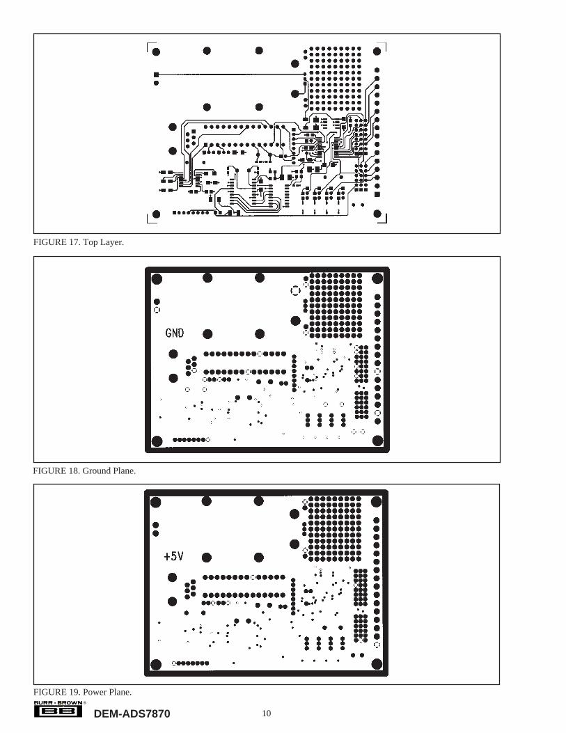
Figures 17 through 21 show the artwork for the four-layer PCB and top silk screen. Table III is the bill of material for the entireassembly.
ITEM QTY REFDES MAKE Part Number VALUE PACKAGE DIGIKEY
1 1 B1 KEYSTONE 1294K BH9V-1 1294K2 3 C1, C12, C14 PANASONIC ECS-T1AX106R 10µF 3528 PCS2106CT3 5 C2, C4, C8, C13, C19 PANASONIC ECU-V1H104KBW 0.1µF CC1206 PCC104BCT4 1 C3 PANASONIC ECU-V1H103KBG 0.01µF CC0805 PCC103BNCT5 4 C5, C6, C10, C11 PANASONIC ECU-V1H220JCV 22pF CC0603 PCC220ACVCT6 5 C7, C9, C15, C16, C18 PANASONIC ECS-T1EY474R 0.47µF 3216 PCS5474CT7 1 C17 PANASONIC ECU-V1H121JCV 120pF CC0603 PCC121ACVCT8 2 D1, D2 LITEON LLSD103A LLSD103A MLL34 LLSD103ACT9 4 D3, D4, D5, D6 CHICAGO_MLI CMD91-21VRC/TR7 — CMD91-21 L62901CT
10 1 D7 DIODES ZMM5232B 5.6V MLL34 ZMM5232BCT11 5 E1, P5, P6, P7, P16 NORCOMP 2163-08-01-P2 — HDR8/2MM-1 2163S-0812 7 E2, E3, E4, E5, E6, E7, E8 NORCOMP 2163-01-01-P2 — EPOINT-M 2163S-0113 1 J1 OST ED555/2DS — ED555/2DS ED151414 1 J2 AMP 520250-2 — AM6-520250 —15 1 J3 OST ED555/16DS — ED555/16DS ED152616 7 P1, P3, P4, P12, P13, P14, P15 NORCOMP 2163-03-01-P2 — HDR3/2MM-1 2163S-0317 2 P2, P8 NORCOMP 2163-02-01-P2 — HDR2/2MM-1 2163S-0218 3 P9, P10, P11 NORCOMP 2163-06-01-P2 — HDR6/2MM-1 2163S-0619 1 R1 PANASONIC ERJ-6ENF4752V 47.5k CR0805 P47.5KCTR20 3 R2, R4, R5 PANASONIC ERJ-6ENF2002V 20.0k CR0805 P20.0KCTR21 2 R3, R13 PANASONIC ERJ-6ENF4022V 40.2k CR0805 P40.2KCTR22 5 R6, R7, R8, R9, R10 PANASONIC ERJ-6ENF3011V 3.01k CR0805 P3.01KCTR23 1 R11 PANASONIC ERJ-6ENF1823V 182k CR0805 P182KCTR24 1 R12 PANASONIC ERJ-6ENF10R0V 10 CR0805 P10.0CTR25 1 U1 NATIONAL LM2936M-5.0 — SO8 —26 1 U2 MICROCHIP PIC16C63-20/JW — DIP28-300 PIC16C63/JW27 1 U3 BURR-BROWN ADS7870 — SSOP28 —28 1 U4 MAXIM MAX3320LCAP — SSO20 —29 1 U5 MICROCHIP PIC16F84-10/SO — SO18W PIC16F84-10/SO30 1 U6 BI_TECH 628L104TR — SO16RP —31 1 Y1 ECS ECS-200-20-4 20.000MHz XTALV X43932 1 Y2 ECS ECS-100-S-4 10.000MHz XTALV X42233 1 — — — PCB — —34 1 — MILL-MAX 115-93-328-41-001 Socket, 28-pin, 300 mil for U2 — ED5828335 7 — Specialty Elect 2JM-G Jumper shunt, 2mm — SPE130236 1 — Comm Con MIJ2MM-06 Jumper shunt block, 2mm, 2 x 6 — —37 1 — Comm Con MIJ2MM-08 Jumper shunt block, 2mm, 2 x 8 — —38 4 — — — Mounting pins - battery clip — —39 1 — — — Serial cable per drawing — —
TABLE III. Parts List.

7®
DEM-ADS7870
20 18 2 3 11 12 16 15 14 13
R5
20.0
kΩ
R4
20.0
kΩ
+5V
2 3 4 5
RS
-232
PO
RT
J252
020-
2
AC
Q_D
AT
A_O
UT
AC
Q_C
NT
RL_
IN
C1+
C1–
C2+
C2–
FO
RC
EO
FF
FO
RC
EO
N
T1_
OU
T
T2_
OU
T
R1_
IN
R2_
IN
1 4 10 9 5 6 7 8
V+
V–
RE
SE
T
INV
ALI
D
T1_
IN
T2_
IN
R1_
OU
T
R2_
OU
T
U4
MA
X33
20
C13
0.1µ
F
9 10 1 27 28 2 3 4 5 6 7
OS
C1_
CLK
IN
OS
C2_
CLK
OU
T
MC
LR_V
PP
RB
6_P
CLK
RB
7_P
DA
TA
RA
0
RA
1
RA
2
RA
3
RA
4
RA
5
+5V
: 20,
GN
D: 8
, 19
RS
-232
to S
PI
Con
trol
ler
+5V
: 19,
GN
D: 1
7
21 22 23 24 25 26 11 12 13 14 15 16 17 18
RB
0
RB
1
RB
2
RB
3
RB
4
RB
5
RC
0
RC
1
RC
2
RC
3_S
CK
RC
4_S
DI
RC
5_S
DO
RC
6_T
X
RC
7_R
X
U2
PIC
16C
63
9 10 23 20 21 22 18 19 16 17 26 27 28 15
RE
SE
T
RIS
E/F
ALL
CS
SC
LK
DIN
DO
UT
OS
C_C
TR
L
CC
LK
CO
NV
ER
T
BU
SY
VR
EF
BU
FIN
BU
FO
UT
/RE
FIN
NC
+5V
: 24,
GN
D: 2
5
11 12 13 14 1 2 3 4 5 6 7 8
DIO
0
DIO
1
DIO
2
DIO
3
LN0
LN1
LN2
LN3
LN4
LN5
LN6
LN7
U3
AD
S78
70
AC
QU
ISIT
ION
CH
IP
C15
0.47
µF+
+5V
+
C5
22pF
C6
22pF
Y1
20M
Hz
C9
0.47
µF
+C
180.
47µF
P3
P4
P8
P2CC
LK
AD
S_R
ES
ET
RIS
E_F
ALL
_N
CO
NV
ER
T
BU
SY
CS
_N
OS
C_C
NT
RL
ST
IM_R
ST
_N
SC
K
SD
I
SD
O
VR
EF
BU
FIN
+5V
CO
M_O
SC
1
CO
M_O
SC
2 SE
L0
SE
L1
P10
HD
R
P6
HD
R
1 2 3 4 5 6 1 2 3 4 5 6 7 8
D3
P12
R6
3.01
kΩ
D4
P13
R7
3.01
kΩ
D5
P14
R8
3.01
kΩ
D6
P15
R9
3.01
kΩ
C3
0.01
µFC
70.
47µF
R1
47.5
kΩ
BU
FO
UT
+5V
FIGURE 14.
8®
DEM-ADS7870
15 16 4 17 18 1 2 3
OS
C1_
CLK
IN
OS
C2_
CLK
OU
T
MC
LR_V
PP
RA
0
RA
1
RA
2
RA
3
RA
4
+5V
: 14,
GN
D: 5
6 7 8 9 10 11 12 13 14
RB
0
RB
1
RB
2
RB
3
RB
4
RB
5
RB
6
RB
7
+V
U5
PIC
16F
84
Stim
ulus
Gen
erat
or
1 2 3 4 5 6 7 8
Stim
ulus
Pro
gram
Por
t
P16
HD
R
+5V
C10
22pF
C11
22pF
Y2
10M
Hz
C17
120p
FR
220
kΩ
R11
182k
Ω
C14
10µF
+R
1340
.2kΩ
R3
40.2
kΩ
10kΩ
20kΩ
1 2 3 4 5 6 7 8
16 15 14 13 12 11 10 9
10kΩ
20kΩ
10kΩ
20kΩ
10kΩ
20kΩ
10kΩ
20kΩ
10kΩ
20kΩ
10kΩ
20kΩ
20kΩ
20kΩ
R10
301k
Ω
D2
D7
5.6V
1 2 3 4 5 6
P9
HD
R
ST
IM_D
IO0ST
IM_W
AV
E
ST
IM_L
EV
EL
ST
IM_R
ES
ET
_N
ST
IM_P
WM
ST
IM_D
IO (
3.0)
ST
IM_+
5V
DA
C0
ST
IM_O
SC
1
ST
IM_O
SC
1
ST
IM_D
IO1
ST
IM_D
IO2
ST
IM_D
IO3
ST
IM_D
IO0
PR
OG
_VP
P
PR
OG
_CLK
PR
OG
_DA
TA
DA
C1
DA
C2
DA
C3
DA
C4
DA
C5
DA
C6
DA
C7
C19
0.1µ
F
ST
IM_D
IO1
ST
IM_D
IO2
ST
IM_D
IO3
1 2 3 4 5 6 7 8
P5
HD
R
62B
L104
FIGURE 15.
9®
DEM-ADS7870
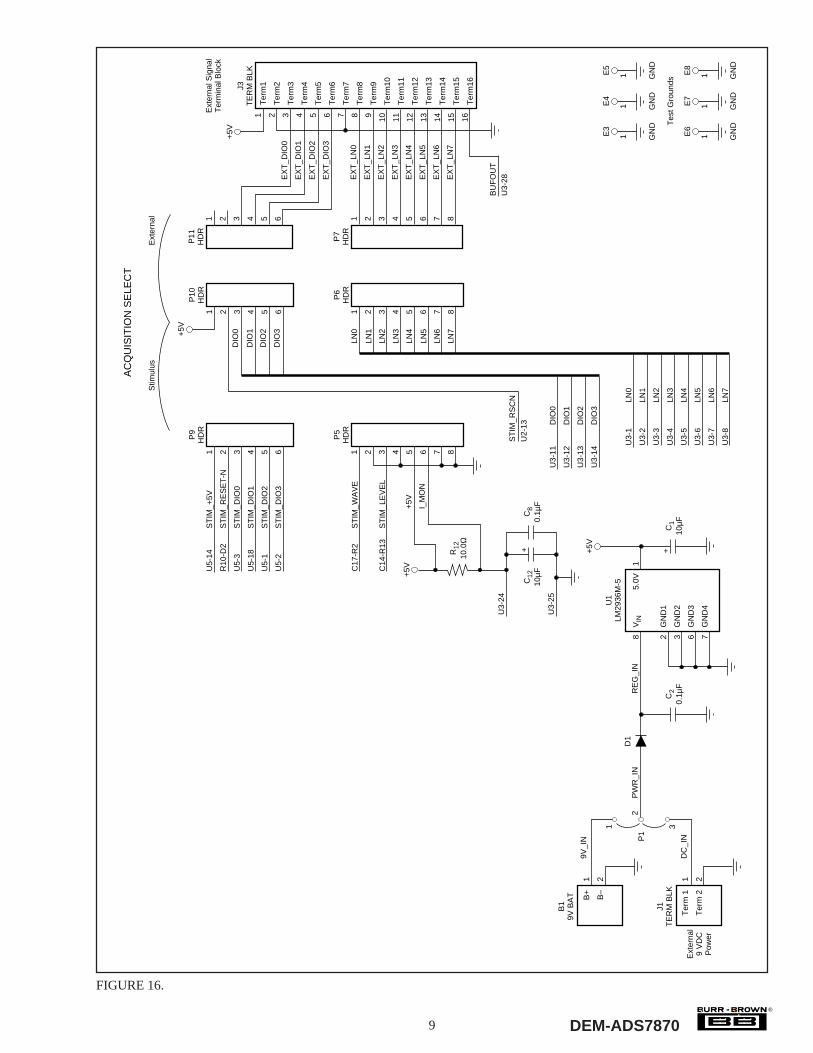
FIGURE 16.
1 2
Ter
m 1
Ter
m 2
Ext
erna
l9
VD
CP
ower
J1T
ER
M B
LK
9V_I
N
DC
_IN
1 2
B+
B–
B1
9V B
AT
P1
1 3
2P
WR
_IN
D1
RE
G_I
N
1 2 3 4 5 6
U5-
14
R10
-D2
U5-
3
U5-
18
U5-
1
U5-
2
ST
IM_+
5V
ST
IM_R
ES
ET
-N
ST
IM_D
IO0
ST
IM_D
IO1
ST
IM_D
IO2
ST
IM_D
IO3
C17
-R2
C14
-R13
ST
IM_W
AV
E
ST
IM_L
EV
EL
P9
HD
R
U3-
11
U3-
12
U3-
13
U3-
14
U3-
24
U3-
25D
IO0
DIO
1
DIO
2
DIO
3
+5V
I_M
ON
ST
IM_R
SC
NU
2-13
BU
FO
UT
U3-
28
U3-
1
U3-
2
U3-
3
U3-
4
U3-
5
U3-
6
U3-
7
U3-
8
LN0
LN1
LN2
LN3
LN4
LN5
LN6
LN7
1 2 3 4 5 6 7 8
P5
HD
R
1 2 3 4 5 6
P10
HD
R
AC
QU
ISIT
ION
SE
LEC
T
Stim
ulus
Ext
erna
l
+5V
DIO
0
DIO
1
DIO
2
DIO
3
LN0
LN1
LN2
LN3
LN4
LN5
LN6
LN7
1 2 3 4 5 6 7 8
P6
HD
R
+5V
1 2 3 4 5 6
P11
HD
R
1 2 3 4 5 6 7 8
P7
HD
R
1 2 3 4 5 6 7 8 9 10 11 12 13 14 15 16
EX
T_D
IO0
EX
T_D
IO1
EX
T_D
IO2
EX
T_D
IO3
EX
T_L
N0
EX
T_L
N1
EX
T_L
N2
EX
T_L
N3
EX
T_L
N4
EX
T_L
N5
EX
T_L
N6
EX
T_L
N7
Ter
m1
Ter
m2
Ter
m3
Ter
m4
Ter
m5
Ter
m6
Ter
m7
Ter
m8
Ter
m9
Ter
m10
Ter
m11
Ter
m12
Ter
m13
Ter
m14
Ter
m15
Ter
m16J3
TE
RM
BLK
Ext
erna
l Sig
nal
Ter
min
al B
lock
E3
GN
D
1
E4
Tes
t Gro
unds
GN
D
1
E5
GN
D
1
E6
GN
D
1
E7
GN
D
1
E8
GN
D
1
C2
0.1µ
FC
110
µF
8 2 3 6 7
VIN
GN
D1
GN
D2
GN
D3
GN
D4U
1LM
2936
M-5
1
+
5.0V
+5V
C8
0.1µ
F
R12
10.0
Ω
C12
10µF
+
+5V
10®
DEM-ADS7870
FIGURE 17. Top Layer.
FIGURE 18. Ground Plane.
FIGURE 19. Power Plane.

11®
DEM-ADS7870
FIGURE 21. Top Side (Silkscreen).
FIGURE 20. Bottom Side.

12®
DEM-ADS7870
APPENDIX B: EMBEDDEDMICRO-CONTROLLERPROGRAMMINGThe embedded controllers can be reprogrammed. The sourcecode for each of the devices is provided in the CD in thefolder titled Support. The files associated with U2, thePIC16C63 are titled “adcmain”.
A PIC16F84 generates the on-board signals. Source codefiles associated with this device contain “stimgen” in thename. Program memory in this device is flash memory andcan be reprogrammed.
PROGRAMMING THE STIMULUS GENERATOR
The DEM-ADS7870 stimulus generator, a MicrochipPIC16F84, is programmed on board through P16, a 2mmspaced 8-pin header. Since only four connections are needed,it is easy to create an adapter for a socket programmer, such asthe PICStart Plus. A diagram of the adapter is shown below.
PIC16F84 PROGRAMMING ADAPTER
The adapter consists of the following parts:1) One 18-pin solder tail DIP socket, DigiKey ED3318 or
equivalent.
2) One 8-pin 2mm solder tail SIP socket, DigiKey 2063S-08or equivalent.
3) Four 10" long pieces of AWG 26 stranded insulatedhookup wire.
4) Small heat shrink tubing.
5) Small wire ties.
To construct the programming adapter:1) Strip and tin the ends of the wires.
2) Slide 3/4" lengths of heat shrink tubing onto the wires.3) Solder the 10" wires to the following points.
SIP socket pin 4 solder tail to DIP socket pin 4 top side.SIP socket pin 5 solder tail to DIP socket pin 12 top side.SIP socket pin 6 solder tail to DIP socket pin 13 top side.SIP socket pin 8 solder tail to DIP socket pin 5 top side.
4) Shrink the heat shrink tubing over the header pin connec-tions.
5) Tie the wires for support.6) Fill pin 2 of the SIP header with epoxy for keying.
(If you plug this in wrong you may blow up the PIC.)
FIGURE 22.
44
5
6
8
2AWG 26 WIRE - 10"
5 13
12

IMPORTANT NOTICE
Texas Instruments and its subsidiaries (TI) reserve the right to make changes to their products or to discontinueany product or service without notice, and advise customers to obtain the latest version of relevant informationto verify, before placing orders, that information being relied on is current and complete. All products are soldsubject to the terms and conditions of sale supplied at the time of order acknowledgment, including thosepertaining to warranty, patent infringement, and limitation of liability.
TI warrants performance of its semiconductor products to the specifications applicable at the time of sale inaccordance with TI’s standard warranty. Testing and other quality control techniques are utilized to the extentTI deems necessary to support this warranty. Specific testing of all parameters of each device is not necessarilyperformed, except those mandated by government requirements.
Customers are responsible for their applications using TI components.
In order to minimize risks associated with the customer’s applications, adequate design and operatingsafeguards must be provided by the customer to minimize inherent or procedural hazards.
TI assumes no liability for applications assistance or customer product design. TI does not warrant or representthat any license, either express or implied, is granted under any patent right, copyright, mask work right, or otherintellectual property right of TI covering or relating to any combination, machine, or process in which suchsemiconductor products or services might be or are used. TI’s publication of information regarding any thirdparty’s products or services does not constitute TI’s approval, warranty or endorsement thereof.
Copyright 2000, Texas Instruments Incorporated