DELAY LINE BASED ADC AND HIGH FREQUENCY PULSE … · converters directly profit from enhanced speed...
82
DELAY LINE BASED ADC AND HIGH FREQUENCY PULSE GENERATION IN ELECTRICAL LC LATICES A Thesis Presented to the Faculty of the Graduate School of Cornell University In Partial Fulfillment of the Requirements for the Degree of Master of Science by Jihyuk Park August 2009
Transcript of DELAY LINE BASED ADC AND HIGH FREQUENCY PULSE … · converters directly profit from enhanced speed...

DELAY LINE BASED ADC AND
HIGH FREQUENCY PULSE GENERATION
IN ELECTRICAL LC LATICES
A Thesis
Presented to the Faculty of the Graduate School
of Cornell University
In Partial Fulfillment of the Requirements for the Degree of
Master of Science
by
Jihyuk Park
August 2009

© 2009 Jihyuk Park

ABSTRACT
This thesis consists of two central goals. The first goal is to introduce an analog-to-
digital converter (ADC) in time-domain resolutions. With the down scaling of the
minimal feature size of modern submicron CMOS technologies, time-to-digital
conversion (TDC) is found very useful in many applications as well as analog-to-
digital converters. This is the case when it is profitable to replace badly scaling analog
circuits with time-to-digital conversions. Since technology scaling implies voltage
scaling while noise does not scale along, variability becomes more important. This
requires more effort to be put into analog circuits that mostly leads to increased power
consumption. However, digital speed does scale with technology. Since time-domain
converters directly profit from enhanced speed performance, switching from the
analog to the digital time domain can significantly reduce the power consumption for
equal performance, especially for designs in sub-100nm technologies.
In general, Analog-to-Digital conversion is performed in three steps: signal difference
amplification, a zero crossing detector, and a succeeding logic encoder. The signal
difference amplification is performed by amplifying the analog voltage (or current) level
by a voltage (or current) amplifier. However, due to the device and voltage scaling in the
CMOS technology, signal difference amplifications become more challenging to achieve
low power consumption with high gain. For a time-domain ADC, as a different solution
for signal difference amplification, delay amplification is used.
In the first chapter, in order to verify the benefit from a time-domain ADC, a 125 MS/s 8-
bit delay-line based ADC is studied and implemented as a circuit using TSMC 65 nm
CMOS process. Simulation results show that, with 1.95 MHz sinusoidal input, the ADC
achieves 7.45 ENOB, a peak differential nonlinearity of 0.095 least significant bit (LSB),

and a peak integral nonlinearity of 0.809 LSB with the power dissipation of 1.8 mW from
a 1.2 V supply voltage.
The second chapter studies the pulse generation in electrical LC lattice. When input
voltage sources are applied to a two-dimensional nonlinear LC lattice, a constructive
interference results in an output signal at the center node with boosted amplitude and
sharpened pulse width compared to its original input signal. The chapter is focused on the
theoretical and experimental study of certain nonlinear wave synthesis phenomena that
appear on the two-dimensional nonlinear LC lattice. It is demonstrated how the
nonlinearity can help in synthesizing high frequency and high amplitude wave pulse at the
central nodes of the lattices. The LC lattice is implemented on PCB composed of voltage-
dependent capacitors and inductors, and for the intense nonlinearity, the capacitor is
carefully chosen. At one horizontal and one vertical boundary, respectively 20 sinusoidal
input sources are applied in phase. The peak-to-peak input amplitude is 1 V, and the
frequency is 13.5 MHz, and the offset voltage for the voltage-dependent capacitor is 200
mV. Measurement results show that the amplitude is boosted to 7.5 V and the pulse width
of the signal is narrowed from 74 ns to 14 ns at the central node.

iii
BIOGRAPHICAL SKETCH
Jihyuk Park received his B.Sc. degree in Electrical and Computer Engineering from
Cornell University in 2007. In 2007, he joined the Ultra-wide band Nonlinear
Integrated Circuits (UNIC) Lab at Cornell University where he studied RFICs such as
60 GHz LNA, mixed signals such as delay-line based ADCs, and the electromagnetic
wave field synthesis observed in nonlinear LC electrical lattices. His research interests
span the general area of analog integrated circuit design with focus on mixed signal
circuits in IC.

iv
Thank you Mother, Father, and my newborn child
And
The sole love in my life,
Yeonjun
빛과 소금이 될 수 있게 해 주신
사랑하는 나의 어머니, 아버지,
그리고 새로 태어날 우리의 아이.
그리고
내가 사랑하는 단 한사람
연준이에게 바칩니다.

v
ACKNOWLEDGMENTS
I would like to acknowledge my advisor, Professor Dr. Ehsan Afshari, who spent
countless hours discussing and helping me in various topics related with the present
thesis, and provided the best education that made me better off in my area of interest.
I also would like to acknowledge a committee member, Professor Dr. Alyssa B. Apsel,
who guided me into the current area of interest, providing the best courses at Cornell
ECE throughout the undergraduate and graduate study.
I would like to thank Dr. Yiorgos Lilis for his help and advice during the LC lattice
project, and Ph.D. student Wooram Lee for his advice on implementing the LC lattice
on chips.
I also would like to thank Ph.D. student Yahya Tousi and Ph. D. student Guansheng Li
for helping me to understand the fundamental concept of the delay line based ADCs.
I also would like to express special thanks to Ph. D. student Omeed Momeni for his
useful suggestions on circuit related topics in general.

vi
TABLE OF CONTENTS
Biographical Sketch iii
Dedication iv
Acknowledgements v
Table of Contents vi
List of Figures ix
List of Tables xi
CHAPTER 1 1
1. Introduction 1
1.1. Time-to-Digital Conversion 1
1.2. Delay-line based ADC 2
1.3. Organization 3
2. Time-interleaved Delay-line based ADC 3
2.1. Principles of operation 3
2.2. The Delay Element: Variable design techniques 4
2.3. Delay Element: Proposed design 7
2.4. Delay element analysis 9
2.5. Time-interleaved structure 10
3. Simulation results 12
3.1. Delay element implementation 12
3.2. Ring structure 15
3.2.1. NAND gate delay 16

vii
3.2.2. Ring size 18
3.3. Differential and Time-interleaved structure 20
3.4. Impact of non-ideality 24
3.5. Comparison to other high resolution ADCs 30
4. Conclusions 31
CHAPTER 2 32
1. Introduction 32
1.1. LC lattices and pulse generation 32
1.2. Potential applications 35
1.3. Prior Art 37
1.4. Organization 37
2. Theory 39
2.1. Nonlinear transmission lines for pulse shaping in silicon 39
2.2. Finite element approach using the method of perturbations 42
2.3. Numerical Approach 48
3. Simulations 49
3.1. Lattice modal analysis 51
4. Experiments 53
4.1. Voltage offset sweep 54
4.2. Input amplitude sweep 56
4.3. Frequency sweep 57
viii
4.4. Optimal results 59
4.5. Energy localization 61
5. Picosecond pulse generation on CMOS 62
6. Conclusions 64
ix
LIST OF FIGURES
[1] Delay-line based ADC diagram 4
[2] Shunt capacitor delay element 5
[3] Supply voltage as the analog input 6
[4] Delay element using variable resistor 7
[5] Current-starved delay element 8
[6] Delay-line composed of delay elements 8
[7] Time-interleaving in time-domain ADCs 11
[8] Delay element topology 13
[9] Delay Vs. Input voltage 14
[10] Ring structure diagram 15
[11] Nonlinearity Vs. NAND gate delays 17
[12] ENOB Vs. NAND gate delays 17
[13] Transfer functions for non-ideal 3-bit ADCs 18
[14] Nonlinearity Vs. ring-delay-line size 19
[15] ENOB Vs. ring-delay-line size 20
[16] Time-interleaved ADC diagram 20
[17] Differential ADC structure 21
[18] 128-point FFT of the proposed ADC 22
[19] DNL of the proposed ADC 23
[20] INL of the proposed ADC 23
[21] Number of delay cells Vs. Input voltage 25
[22] Setup for the variation simulations 26
[23] Supply voltage variation simulation 27
[24] Temperature variation simulation 28

x
[25] Nonlinear 2-D LC lattice diagram 33
[26] Constructive interference 34
[27] Terahertz gap 35
[28] Terahertz applications 37
[29] 1-D nonlinear transmission line 39
[30] soliton generation 41
[31] Modeling 2-D LC lattice 45
[32] C-V characteristic curves 50
[33] Eigen mode analysis of the LC lattice 52
[34] LC lattice on PCB 53
[35] Boost ratio Vs. varactor bias voltage 55
[36] Boost ratio Vs. input amplitude 56
[37] Boost ratio Vs. input frequency 57
[38] Optimized output responses on PCB 60
[39] Constructive interference MATLAB 3-D graph 60
[40] Energy localization comparison 62
[41] Optimized output responses in IC 63

xi
LIST OF TABLES
[1] Size of the proposed delay element 15
[2] Corner simulation results 24
[3] Voltage variation simulation results 27
[4] Temperature variation simulation results 29
[5] Performance of the proposed ADC 29
[6] Performance comparison chart 30
[7] Component parameters of LC lattice on PCB 50
[8] Pulse generation on PCB 59
[9] Pulse generation on IC 63

1
CHAPTER 1
DELAY-LINE BASED ADC
1 Introduction
1.1 Time-to-Digital Conversion
Time-to-Digital converters have been reported for various applications [1]. With the
downscaling of the minimal feature size of modern submicron CMOS technologies,
TDCs are found very useful in many applications as well as analog-to-digital
converters. This is the case when it is profitable to replace badly scaling analog
circuits with TDCs. Since technology scaling implies voltage scaling while noise does
not scale along, variability becomes more important. This requires more effort to be
put into analog circuits which mostly leads to increased power consumption [2], [3].
Digital speed, however, does scale with technology. Since time-domain converters
directly profit from enhanced speed performance, switching from the analog to the
(digital) time domain can significantly reduce the power consumption for equal
performance, especially for designs in sub-100nm technology nodes. Furthermore,
people have realized that we are facing a new paradigm [4]:
In a deep-submicron CMOS process, time-domain resolution of a digital signal
edge transition is superior to voltage resolution of analog signals.
This is in clear contrast with the older process technologies, which rely on a high
supply voltage (originally 15 V, then 5V, and finally 3.3 V and 2.5 V) and a
standalone configuration with few extraneous noise sources in order to achieve a good
signal-to-noise ratio and resolution in the voltage domain, often at a cost of long

2
settling time. In a deep-submicron process, with its low supply voltage (at and below
1.5 V), relatively high threshold voltage (0.5 V and often higher due to the MOSFET
body effect), the available voltage headroom is quite small for any sophisticated
analog functions. Moreover, considerable switching noise of substantial digital
circuitry around makes it harder to resolve signals in the voltage domain. On the other
hand, the switching characteristics of a MOS transistor, with rise and fall times on the
order of tens of picoseconds bring more precise resolution in the time-domain
conversions.
1.2 Delay-line based ADC
In general, Analog-to-Digital conversion is performed in three steps [5]: signal
difference amplification, a zero crossing detector, and a succeeding logic encoder. The
analog signal difference amplifications are performed by amplifying the analog
voltage (or current) level by a voltage (or current) amplifier. However, as mentioned
in section 1.1, due to the device and voltage scaling in the CMOS technology, signal
difference amplifications become more challenging to achieve low power
consumption and high gain. For a time-domain ADC, such as a delay-line based ADC,
as a different solution for signal difference amplification, delay amplification is used.
A recent work [6] showed that the delay amplification have significantly better
performance for the high speed and low resolution ADCs. In a delay-line based ADC,
an applied pulse is propagated in a variable delay line and its delay is quantized after a
certain amount of time. Since the delay-line based ADC utilizes gate delays of rise and
fall time, the scaling of CMOS which gives smaller delay steps is a fundamental
advantage to it as opposed to traditional analog circuits.

3
1.3 Organization
The applied concept and the architecture of the proposed ADC are discussed in section
2. After the idea of the delay amplification is discussed in section 2.1, since the delay
element is the key unit to this architecture, the behavior of the delay element is
presented in section 2.2 and the digitization of the number of stages of a delay line is
presented in section 2.3. Furthermore, the benefits from using the time-interleaved
architecture in the time-domain ADCs are discussed in section 2.3.
Simulation results of the proposed architecture are discussed in section 3. A plot for
the delay as a function of the input voltage is also presented in section 3.1. This plot
gives the analog input nMOS device bias point and the input range for the optimal
performance given specifications. In section 3.2, a brief comparison between a ring
structure using a delay loop and a linear structure using a delay-line is presented.
Simulation results of the final structure are shown in section 3.3 and impact of non-
ideality is discussed in section 3.4. In section 3.5, the performance of this ADC is
compared to those other state-of-art ADCs.
2 Time-interleaved Delay-line based ADC
2.1 Principles of operation
The idea of delay amplification is to apply a pulse to a delay line (or loop) and
measure the distance in terms of number of delay elements the signal passes in a
certain amount of time. This number is proportional to the time window (or the
sampling period). In Figure1, the concept of the quantization method is shown.
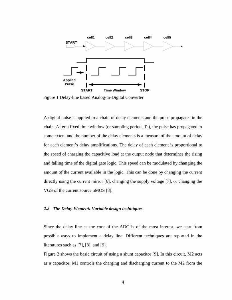
4
A digital pulse is applied to a chain of delay elements and the pulse propagates in the
chain. After a fixed time window (or sampling period, Ts), the pulse has propagated to
some extent and the number of the delay elements is a measure of the amount of delay
for each element’s delay amplifications. The delay of each element is proportional to
the speed of charging the capacitive load at the output node that determines the rising
and falling time of the digital gate logic. This speed can be modulated by changing the
amount of the current available in the logic. This can be done by changing the current
directly using the current mirror [6], changing the supply voltage [7], or changing the
VGS of the current source nMOS [8].
2.2 The Delay Element: Variable design techniques
Since the delay line as the core of the ADC is of the most interest, we start from
possible ways to implement a delay line. Different techniques are reported in the
literatures such as [7], [8], and [9].
Figure 2 shows the basic circuit of using a shunt capacitor [9]. In this circuit, M2 acts
as a capacitor. M1 controls the charging and discharging current to the M2 from the
START
cell1 cell2 cell3 cell4 cell5
Applied
Pulse
Time WindowSTART STOP
Figure 1 Delay-line based Analog-to-Digital Converter

5
NOR gate. The M1 gate voltage, Vctrl, controls the (dis)charge current. As a
consequence, the NOR gate delay can be controlled.
Figure 2 Shunt capacitor delay element
Watanabe el al [7] have proposed an architecture for fully digital ADCs. The main
building block of this architecture is a chain of delay elements forming a delay unit
[10] as show in Figure 3. The input analog voltage Vin is used as the supply voltage of
the inverters. It is well know that the delay of an inverter is a function of its supply
voltage [11]. Hence In pulse experiences a delay, which is a function of Vin. Due to
the delay of each delay element, the rising edge of pulse In takes some time to reach
the last delay element and measurement of this delay can provide the digital data.
However, since the input voltage provides the supply voltage of the delay elements,
this architecture has two negative consequences. First, it puts a huge load on Vin. The
second drawback is that as the input voltage varies the voltage swing at the output of
the delay elements changes. When Vin drops below Vdd, the high level at the output of
each of the delay elements is no longer Vdd that causes two problems. First, it makes
reading the output of the delay elements more complicated. Secondly, it increases the
leakage current in the succeeding stages connected to the output of delay elements. To
clarify this point, note that the output of each of the delay elements is connected to the
input of a latch. Since the supply voltage in the latch is not dependent on the analog

6
input voltage and thus is not changing, when the Vin drops below Vdd, the output of
the delay element cannot completely turn off the input pMOS transistor in the latch.
This increase the leakage current of these transistors when they are supposed to be off
and consequently the power consumption increases.
Figure 3 Delay is modulated by the supply voltage as the analog input
Another technique for implementing a digitally controlling delay element is illustrated
in Figure 4. In this circuit, a variable resistor is used to control the delay [8]. A stack
of n rows by m columns of nMOS transistors is used to make a variable resistor. This
resistor subsequently controls the delay of M1. In the circuit of Figure 4, only the
rising edge of the output can be changed with the input vector. Another stack of
pMOS transistors can be used at the source of the pMOS transistor, M2, to have
control over the falling edge delay.

7
Figure 4 The delay element using variable resistor
2.3 Delay Element: Proposed design
Another method to implement the delay element is the current starved technique as
shown in Figure 5 [12]. We call this a current-starved inverter since the mechanism
for controlling the delay of each inverter is to limit the current available to discharge
the load capacitance of the gate.
In this modified inverter circuit, the maximal discharge current of the inverter is
limited by adding an extra series device. Note that the low-to-high transition on the
inverter can also be controlled by adding a pMOS device in series with M3. The added
nMOS transistor M1, is controlled by an analog control voltage VIN, which
determines the available discharge current. Lowering VIN reduces the discharge
current and, hence, increases falling time at the output node. The ability to alter the
propagation delay per stage allows us delay amplification of the ADC structure. The

8
control voltage is generally set by using feedback techniques. Under low-operating
current levels, the current starved inverter may suffer from slow fall times at its output.
This can result in significant short-circuit current. We solve this problem by feeding
its output into a CMOS inverter, or better Schmitt trigger.
For this project, the current-starved technique is mainly used for the implementation of
the delay element.
Figure 5 The proposed current-starved delay element
Figure 6 Delay-line structure composed of the unit delay elements
OUTIN
VIN
VDD
CL
C1M1
M2
M3
START
VIN
Delay Cell
1 1 1 0 0

9
2.4 Delay element analysis
In this section, we will discuss the delay element more in detail. In Figure 6, VIN is the
analog input voltage and while START is ON, the pulse is propagating into the delay
line. We denote the time while START is ON as the time window (or sampling period,
T) and the delay per element as D(VIN).
At the end of the time window, a number of delay elements are set to one as in (1).
(1)
x is the integer part of x .
Generally, D(VIN) can be assumed to be monotone in the range of interest ba VV , ,
and hence )(VINNQ ranges between )( aVN and )( bVN , resulting in a resolution
of about
(2)
where R is the number of bits of the digital output and *V is a constant in ba VV , . (2)
shows that a delay element with small delay and sensitive to the control voltage is
desirable to achieve high resolution. Besides (2) reveals the basic trade-off between
time and resolution. That is, the number of bits R can be increased at the cost of a
larger time interval T or slow sampling rates.
In terms of linearity, it is desirable to have delay elements with
(3)
)()()(
VIND
TVINNVINNQ
*
)(
)(
1log)()(log
222
VV
babadV
VdD
VDVVTVNVNR
0
0)(VVIN
DVIND
10
where 0D and 0V are constants. However, it is usually the case that this relation can
only be approximated within a relatively small range ba VV , . In this case, another
trade-off between speed and linearity comes into play: as in (2), a high conversion
speed requires the time interval T to be small while a good linearity requires the
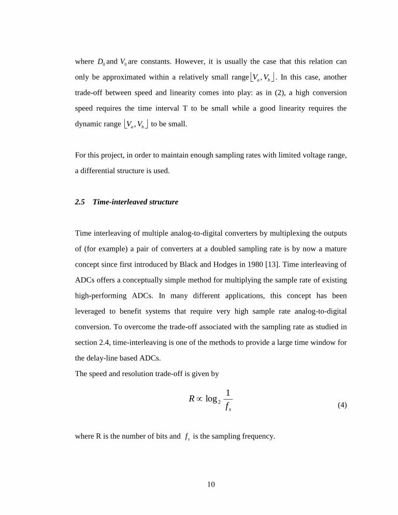
dynamic range ba VV , to be small.
For this project, in order to maintain enough sampling rates with limited voltage range,
a differential structure is used.
2.5 Time-interleaved structure
Time interleaving of multiple analog-to-digital converters by multiplexing the outputs
of (for example) a pair of converters at a doubled sampling rate is by now a mature
concept since first introduced by Black and Hodges in 1980 [13]. Time interleaving of
ADCs offers a conceptually simple method for multiplying the sample rate of existing
high-performing ADCs. In many different applications, this concept has been
leveraged to benefit systems that require very high sample rate analog-to-digital
conversion. To overcome the trade-off associated with the sampling rate as studied in
section 2.4, time-interleaving is one of the methods to provide a large time window for
the delay-line based ADCs.
The speed and resolution trade-off is given by
(4)
where R is the number of bits and sf is the sampling frequency.
sfR
1log2
11
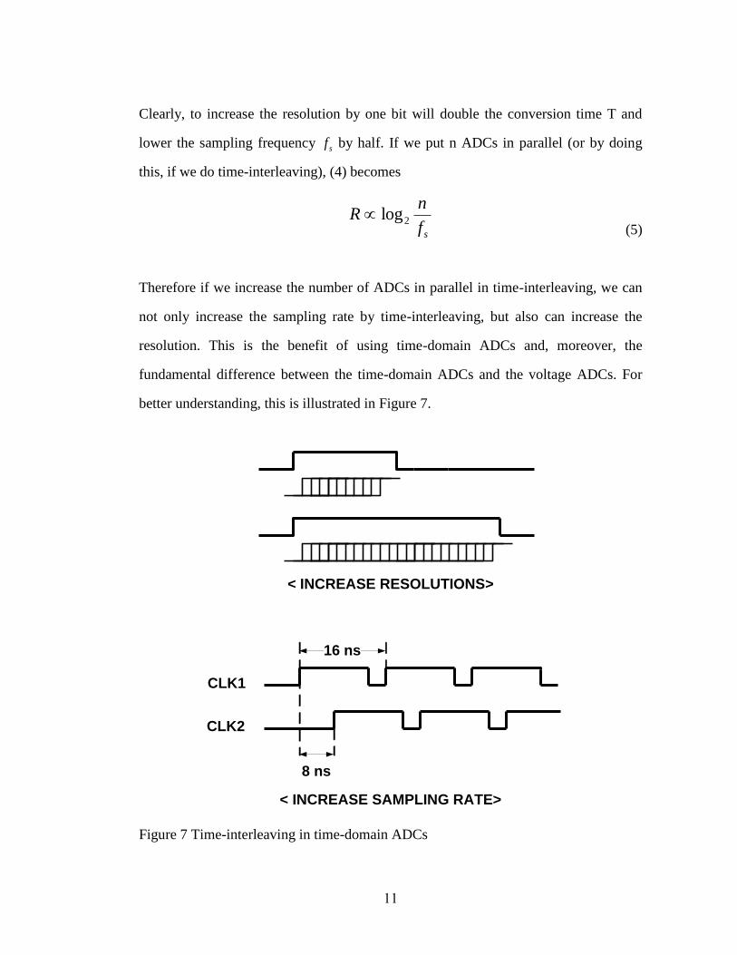
Clearly, to increase the resolution by one bit will double the conversion time T and
lower the sampling frequency sf by half. If we put n ADCs in parallel (or by doing
this, if we do time-interleaving), (4) becomes
(5)
Therefore if we increase the number of ADCs in parallel in time-interleaving, we can
not only increase the sampling rate by time-interleaving, but also can increase the
resolution. This is the benefit of using time-domain ADCs and, moreover, the
fundamental difference between the time-domain ADCs and the voltage ADCs. For
better understanding, this is illustrated in Figure 7.
Figure 7 Time-interleaving in time-domain ADCs
sf
nR 2log
CLK1
CLK2
16 ns
8 ns
< INCREASE RESOLUTIONS>
< INCREASE SAMPLING RATE>

12
3 Simulation results
3.1 Delay element implementation
A prototype of the delay element is implemented with TSMC 65 nm CMOS process.
Its block diagram and equivalent RC circuit diagram is shown in Figure 8. To design
the delay elements the following conditions are considered for the better performance:
Minimize the power consumption through the whole operating input voltage
range
The delay should be a strong function of the input voltage
The delay range should be enough to meet the required resolution
Ideally we want the number of delay elements to be a linearly proportional to
the input voltage
To satisfy above conditions, first of all, we want M1 in Figure 8 to be operating in
linear region in order for the delay element to minimize the current flowing into itself
and to have a linearly proportional relationship between the delay and the input
voltage for the better linearity as one can see in (6) and (7).
(6)
(7)
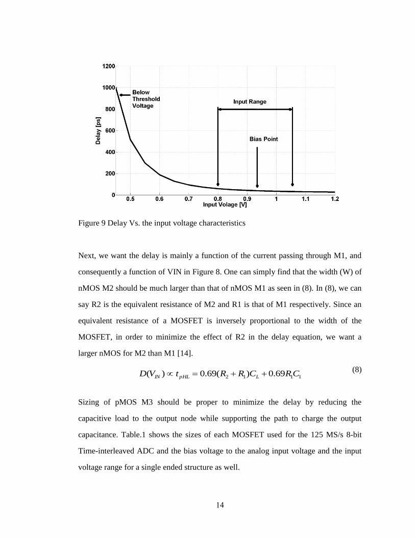
One drawback of this idea is that the input range and the delay range are small since
the linear region of current source (M1) is not wide. However, the input range can be
)(
)(
)()(
THINn
DDLDDLpHLIN
THINnTHGn
VVL
Wk
VC
I
VCtVD
VVL
WkVV
L
WkI
ININ
IN
IN
VVN
VD
TVN
)(
)()(

13
doubled when we use a differential structure. Figure 9 shows the delay of the proposed
delay element from Cadence simulations. It is noteworthy that when the control (or
analog input) voltage is smaller than the threshold, the device enters the subthreshold
region. This results in large variations of the propagation delay, as the drive current is
exponentially dependent on the drive voltage. When operating in this region, the delay
is very sensitive to variations in the control voltage and hence to noise
For the rest of the simulations, the bias voltage to the analog input nMOS is set to 930
mV.
Figure 8 The delay element topology used in this project
C1R1
R2
CL
Equivalent
OUTIN
VIN
VDD
CL
C1M1
M2
M3
14
Figure 9 Delay Vs. the input voltage characteristics
Next, we want the delay is mainly a function of the current passing through M1, and
consequently a function of VIN in Figure 8. One can simply find that the width (W) of
nMOS M2 should be much larger than that of nMOS M1 as seen in (8). In (8), we can
say R2 is the equivalent resistance of M2 and R1 is that of M1 respectively. Since an
equivalent resistance of a MOSFET is inversely proportional to the width of the
MOSFET, in order to minimize the effect of R2 in the delay equation, we want a
larger nMOS for M2 than M1 [14].
(8)
Sizing of pMOS M3 should be proper to minimize the delay by reducing the
capacitive load to the output node while supporting the path to charge the output
capacitance. Table.1 shows the sizes of each MOSFET used for the 125 MS/s 8-bit
Time-interleaved ADC and the bias voltage to the analog input voltage and the input
voltage range for a single ended structure as well.
1112 69.0)(69.0)( CRCRRtVD LpHLIN

15
For each MOSFET, the minimum length for the process is used, which is 60 nm.
Table 1 Size of MOSFETs in the delay element
MOSFET W (Width)
M1 (nMOS) 3 µm
M2 (nMOS) 7 µm
M3 (pMOS) 7 µm
Bias point 930 mV
Single-ended input voltage range 800 mV – 1060 mV
3.2 Ring structure
8-bit resolution requires that the delay line has at least 28 = 256 stages of delay
elements. If the resolution increases to 10 or 14 bits which are necessary for a sensor
ADC, the required stages reaches even to 20,000 to 200,000 stages. In order to reduce
the size of the circuit, a structure has been considered which uses a ring-delay-line
(RDL) as the delay circuit to determine the frequency of the delay pulse [15], [16], as
shown in Figure 10.
Figure 10 Block diagram of the ring-delay-line
START
VIN

16
Since there are a few delay elements, the area voltage-modulated by the input voltage
VIN can be extremely small so as to match well the mutual characteristics of the delay
elements.
3.2.1 NAND gate delay
However, this structure requires a careful design for the NAND gate at the beginning
of the RDL. The delay characteristic of NAND gate is constant throughout the input
voltage range and, thus, the quantizer will deviate from the ideal linear curve as the
constant delay is being added to the voltage-dependent delay generated by delay
elements at every turn. To compensate the non-ideal effects, we could modify the
NAND gate so that it has delay characteristics as a function of input voltages, and
replace the whole delay elements by the same NAND gates. By doing this, we can get
rid of the nonlinearity due to the sole use of NAND gate in Figure 10. However, for
high resolutions, minimum delay is critical as seen (1) with a given sampling period,
and generally the delay in a NAND gate is bigger than that in an inverter buffer.
Therefore careful study in trade-off between a NAND gate and an inverter buffer as a
delay element is required to maximize the performance. A further study regarding this
issue is not done in detail in this thesis, and remains as a future work.
Figure 11 and Figure 12 show the effects of the delay in NAND gate to the dynamic
and static linearity errors. Ideally, since no non-ideal effect is desired, the best result
should be supposed to appear at the zero delay. However, note that the delay element
is optimized to perform the best at the delay of 5 ps from the initial design level.
Nevertheless, one can easily see the non-ideal effect significantly degrades the
performance as the delay in the NAND gate increases as expected.

17
Simulation is done with TSMC 65 nm CMOS process. The sampling frequency is125
MS/s and the desired resolution is 8 bits. In order to limit the effect of the delay of
NAND gate, an ideal NAND component from the Cadence library is used.
Figure 11 The differential (DNL) and integral (INL) nonlinearity variation as a
function of NAND gate delays
Figure 12 The NAND gate delay dependency of ENOB
18
3.2.2 Ring size
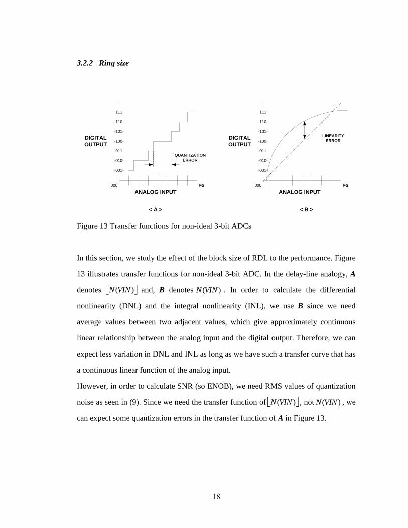
Figure 13 Transfer functions for non-ideal 3-bit ADCs
In this section, we study the effect of the block size of RDL to the performance. Figure
13 illustrates transfer functions for non-ideal 3-bit ADC. In the delay-line analogy, A
denotes )(VINN and, B denotes )(VINN . In order to calculate the differential
nonlinearity (DNL) and the integral nonlinearity (INL), we use B since we need
average values between two adjacent values, which give approximately continuous
linear relationship between the analog input and the digital output. Therefore, we can
expect less variation in DNL and INL as long as we have such a transfer curve that has
a continuous linear function of the analog input.
However, in order to calculate SNR (so ENOB), we need RMS values of quantization
noise as seen in (9). Since we need the transfer function of )(VINN , not )(VINN , we
can expect some quantization errors in the transfer function of A in Figure 13.
111
110
101
100
011
010
001
FS
DIGITAL
OUTPUT
000
ANALOG INPUT
QUANTIZATION
ERROR
111
110
101
100
011
010
001
FS
DIGITAL
OUTPUT
000
ANALOG INPUT
LINEARITY
ERROR
< A > < B >
19
(9)
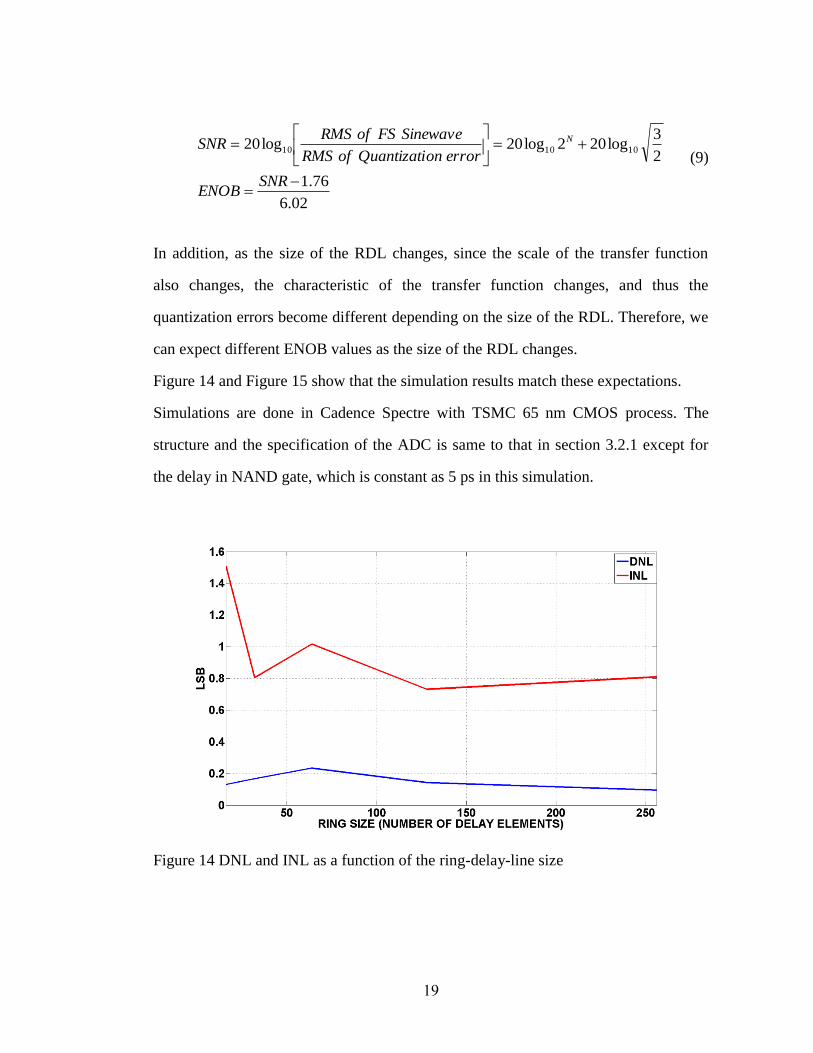
In addition, as the size of the RDL changes, since the scale of the transfer function
also changes, the characteristic of the transfer function changes, and thus the
quantization errors become different depending on the size of the RDL. Therefore, we
can expect different ENOB values as the size of the RDL changes.
Figure 14 and Figure 15 show that the simulation results match these expectations.
Simulations are done in Cadence Spectre with TSMC 65 nm CMOS process. The
structure and the specification of the ADC is same to that in section 3.2.1 except for
the delay in NAND gate, which is constant as 5 ps in this simulation.
Figure 14 DNL and INL as a function of the ring-delay-line size
02.6
76.1
2
3log202log20log20 101010
SNRENOB
erroronQuantizatiofRMS
SinewaveFSofRMSSNR N

20
Figure 15 Effective number of bits (ENOB) as a function of the ring size
3.3 Differential and Time-interleaved structure
In order to implement 125 MS/s 8-bit delay-line ADC, a time-interleaved structure is
designed as seen Figure 16.
Figure 16 Increase in the sampling rate in the time-interleaved structure
S/H1
S/H2
ADC1
ADC2
ANALOG INPUTCLK1
CLK2
CLK1
CLK2
16 ns
8 ns

21
This architecture does not have a high speed S/H just after the analog input to remove
the limit of the bandwidth and linearity of the high speed S/H. Instead of having a fast
S/H operating at f, )2( NN sub-sampled S/H circuits may be used for N sub-ADCs,
reducing the highest sampling rate to fs/N and making the architecture scalable to
higher sampling rates. Although we still need to drive the input to the load of sub-
ADC channels, this architecture is more feasible especially when the high speed ADCs
are desired as in [17].
For sub-ADC design, a differential structure is used in order to increase the available
input voltage range since the delay elements are biased to operate in triode region,
which limit the analog input voltage range.
Figure 17 shows the differential structure used for the sub-ADCs.
Figure 17 Differential structure diagrams
Sampling period
START
VIN+
COUNTER
LATCHLATCH
ENCODER
LSBs MSBs
8 bits
SAMPLE
Sampling period
START
VIN-
COUNTER
LATCHLATCH
ENCODER
LSBs MSBs
SAMPLE

22
In this project, a 125 MS/s 8-bit time-interleaved ADC is implemented using TSMC
65nm CMOS process. For the sample and hold circuits, ideal components from the
library in Cadence.
The fast Fourier transform (FFT) results of the proposed ADC for an input signal with
the frequency of 1.95 MHz are shown in Figure 18. Based on this simulation result,
ENOB is calculated to be 7.45 bits with SFDR = 51 dB and SNDR = 47 dB. Figure 19
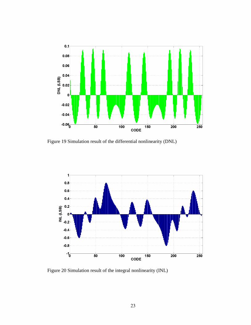
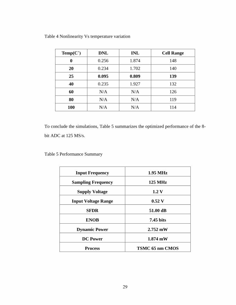
and Figure 20 show the differential nonlinearity (DNL) and the integral nonlinearity
(INL) with a differential ramp signal of the range from -0.26 V to +0.26 V. The peak
DNL is 0.095 LSB and the peak INL is 0.809 LSB.
For the rest of the simulations, the same circuit and the same input signal were
retained.
Figure 18 128-point FFT of the reconstructed sinusoidal input signal after processed
by ADC and DAC with the input frequency of 1.95 MHz
23
Figure 19 Simulation result of the differential nonlinearity (DNL)
Figure 20 Simulation result of the integral nonlinearity (INL)

24
3.4 Impact of non-ideality
There are several factors that will degrade the performance of the ADC, which include
variations in process, voltage-supply and temperature (PVT). PVT variations that
cause non-ideal characteristics of the delay element are critical to the ADC
performance and must be minimized. While the differential circuit technique can
alleviate the effect of PVT variation to some extent, a calibration circuit will be
necessary in practical systems to save the correct characteristics of the delay element.
Process variations are simulated in Cadence by modifying sections in model files in
the model library setup: ff(fast nMOS, fast pMOS), ss(slow nMOS, slow pMOS),
fs(fast nMOS, slow pMOS), sf(slow nMOS, fast pMOS), and tt(typical nMOS, typical
pMOS). Figure 21 and table 2shows the simulation results of the corner variation.
Figure 21 shows that in case of fast nMOS and slow pMOS the system fails to
generate enough linearity for the given resolution, which is 8-bit in this project.
Table 2 Nonlinearity Vs Corner simulations
DNL INL Cell Range
TT 0.095 0.809 278
SS 0.473 1.839 270
FF 0.131 1.073 280
SF 0.186 1.320 302
FS N/A N/A 250

25
Figure 21 Process variation using corner simulations. Top shows the delay cells
characteristics as a function of differential input voltages at normal state, while bottom
shows the results of the corner simulations

26
Supply voltage variations are also critical in sense that the supply voltage directly
changes the available current in the delay element and, thus, changes the delay in the
delay element. Figure 22 illustrates the simulation setup for both the supply voltage
variation simulation and the temperature variation simulation. The simulation results
are shown in Figure 23 and Table 3 with sweeping the supply voltage from 0.9 V to
1.5 V.
Figure 22 Simulation setup for the variation simulations

27
Figure 23 Number of the available delay elements as a function of the supply voltage
Table 3 Nonlinearity Vs supply voltage variation
VDD (V) DNL INL Cell Range
0.9 N/A N/A 58
1.0 N/A N/A 88
1.1 N/A N/A 115
1.2 0.095 0.809 139
1.3 0.126 0.902 156
1.4 0.130 0.825 168
1.5 0.094 0.618 177

28
Finally, the non-ideality due to the temperature variation is simulated as seen in Figure
24 and Table 4. If the temperature is low, then the delay would be low due to the
mobility variation. On the contrary, if the temperature increases, the delay would
increase consequently and the changed delay characteristic would not be proper to
generate enough linearity given resolution and sampling period.
Figure 24 Number of the available delay elements as a function of the supply voltage
29
Table 4 Nonlinearity Vs temperature variation
Temp(C˚) DNL INL Cell Range
0 0.256 1.874 148
20 0.234 1.702 140
25 0.095 0.809 139
40 0.235 1.927 132
60 N/A N/A 126
80 N/A N/A 119
100 N/A N/A 114
To conclude the simulations, Table 5 summarizes the optimized performance of the 8-
bit ADC at 125 MS/s.
Table 5 Performance Summary
Input Frequency 1.95 MHz
Sampling Frequency 125 MHz
Supply Voltage 1.2 V
Input Voltage Range 0.52 V
SFDR 51.00 dB
ENOB 7.45 bits
Dynamic Power 2.752 mW
DC Power 1.874 mW
Process TSMC 65 nm CMOS

30
3.5 Comparison to other high resolution ADCs
We can define the Figure of merit with the help of [18] as:
(10)
This ADC yields a FOM of 482 fJ/conversion step when the input frequency is 31.25
MHz and ENOB is 6.9 bits. The comparison of this design to other ADCs shown in
Table 6 shows its superior performance compared to most of the conventional
structures.
Table 6 Performance comparison chart
Ref. Technology FOM [ pJ/conversion]
[19] 0.6 µm 88
[20] 0.5 µm 794
[21] 0.35 µm 529
[22] 0.35 µm 30
[23] 0.18 µm 2.5
[24] 0.13 µm 0.54
This work 0.065 µm 0.48
),2min(2 samplein
ENOB ff
powerFOM

31
4 Conclusions
A low power ADC with time domain resolution of digital signals is introduced with
digital CMOS process. As a case study, a 125 MS/s 8bit delay-line based time-
interleaved ADC was designed in TSMC 65 nm CMOS process. While time-
interleaving in conventional ADCs increases only sampling rates, with delay-line
based ADCs, we can achieve high-resolution ADCs with high sampling rates thanks to
the time-interleaving.

32
CHAPTER 2
HIGH FREQUENCY PULSE GENERATION IN ELECTRICAL LATTICE
1 Introduction
1.1 LC lattices and pulse generation
Lately there has been increasing interest in implementing devices operating in the
terahertz frequency band (100 GHz – 10THz) [25] with exciting potential applications
in a variety of areas, such as spectroscopy [26], communications [27], and imaging
[28]. However, it is quite challenging to generate signals in the terahertz band in
today’s commercial CMOS processes, given the maximum operating frequencies of
most MOS transistors ranges between 200 GHz and 300 GHz.
One particularly useful method of going beyond the frequency limit involves the use
of nonlinear devices to translate the functionality of lower frequency electronics into
the terahertz band [29]. An extensively studied example is the nonlinear transmission
line, which consists of inductors and voltage-dependent capacitors and has been
implemented on Si substrates, showing the capability of generating high-order
harmonics of the input signals [30].
For more output power at high frequencies, a two-dimensional circuit topology of the
nonlinear LC lattices has been also studied and theoretically described how
nonlinearity of the lattice medium significantly boosts the input signal by nonlinear
constructive interference [31].
A two-dimensional nonlinear LC lattice is an electrical circuit consisting of identical,
repeated in two dimensions, small LC elements. Each LC element consists of two

33
coils and a non-linear capacitor or varactor connected as illustrated in Figure 25. The
inputs of the lattice are voltage sources applied at the left and bottom boundaries. The
behavior of a LC-lattice emulates the behavior of a two-dimensional wave medium,
producing two or more wave fronts that propagate towards the center of the lattice.
Furthermore, for certain configurations of inductors and voltage-dependent capacitors,
and incident angle, the lattices exhibit rich nonlinear behavior. This behavior is the
topic of the present chapter.
Figure 25 Nonlinear two-dimensional LC lattice
If the capacitors of the lattice of the lattice are constant with respect to their applied
voltage, the lattice dynamics are linear. Assuming the inputs are all in phase and that
they all have equal amplitude A, we find at a fixed time T > 0 that the peak output
voltage is equal to mA for some positive number m that does not depend on A. This is
the meaning of linearity: if we double the amplitudes of all the inputs, we expect the
outputs to also double in amplitude. The linear nature of the lattice ensures also that
the frequencies of the signals observed in the intermediate nodes appear also in the
inputs.

34
However, if the capacitance value changes with respect to their applied voltage, the
lattice emulates a nonlinear wave medium that is characterized by a wave-speed that
depends on the wave amplitude. In this case, due to the nonlinearity, the amplification
observed in the center of the lattice can be considerably higher than that of the linear
case. Additionally, higher frequency components than the input frequencies appear in
the central nodes. By biasing the capacitors using the external DC voltage source at a
certain optimal operating voltage range, the input pulses generated by the voltage
sources in the boundaries can be added in the central nodes and significantly amplified
and sharpened. This nonlinear constructive wave synthesis phenomenon can be
explained by the high amplitude and high frequency harmonic generation, or pulse
narrowing, observed in such lattices and is illustrated in the Figure 26.
Figure 26 Two-dimensional constructive interference

35
The high amplitude and high frequency harmonic generation that characterizes the
behavior of a nonlinear two-dimensional LC lattice can be studied theoretically using
the method of perturbations [32]. In order to do that, every LC unit is treated as a
finite element with governing equations, the Kirchhoff’s voltage and current laws.
These equations are assembled into a unique system equations referring to the whole
lattice.
1.2 Potential applications
The high frequency and high amplitude harmonic generation ability of the examined
nonlinear LC lattice holds a promise of creating electronic devices which will bridge
the terahertz gap [29] (Figure 27).
Figure 27 Terahertz gap with respect to source technology

36
As is evident from Figure 27, the performance of the diode multipliers gradually
degrades as the frequency is increased. This is true of all electronic circuits in this
frequency band and is due to a variety of both fundamental and practical limitations.
All electronic devices are limited by parasitic circuit elements such as series resistance
and shunt capacitance. As the operating frequency increases, terahertz diodes must be
made smaller to reduce junction capacitance, but this increases series resistance,
thereby resulting in a fundamental design tradeoff.
Above 2 THz, the quantum cascade (QC) lasers dominate [33], [34]. They are
particularly useful in the infrared bands and in the higher end of the terahertz band.
However, below about 4 THz, they require cryogenic cooling to achieve continuous
wave (CW) operation. QC lasers will play a major role in the development of the
terahertz field. However, there are fundamental physical obstacles that will likely
prevent them from operating in CW mode below a few terahertz, especially if room-
temperature operation is required. Also, issues such as frequency stability, tuning
bandwidth, and lifetime have not yet been sufficiently addressed in this emerging
technology.
Radiation in terahertz range can provide high resolution with minimum health risks
since it is not ionizing. Therefore, nonlinear devices such as nonlinear two-
dimensional LC lattices could be embedded in existing devices and expand further
their frequency and power performance, materializing the advantages the terahertz
technology can offer. Such devices could be oscillators or frequency multipliers for
high data rate communication and imaging systems, which can be used for security
and medical purpose as Figure 28.

37
Figure 28 Terahertz applications
1.3 Prior Art
Many authors have studied the solutions of the governing equations of two-
dimensional nonlinear lattices. In the most recent work, finally the equations
governing the behavior of a two-dimensional nonlinear LC lattice are derived and
solved using the method of perturbations, for specific types of nonlinearities in [31].
Experimental works on one [30] and two-dimensional [35] nonlinear LC lattices have
also been performed.
1.4 Organization
First, in section 2.1, a nonlinear transmission lines for pulse narrowing in Si substrate
is shown. A soliton generation is studied on a 1-D nonlinear transmission line that is
composed of voltage-dependent capacitors and inductors.

38
In section 2, the theoretical basis for the development of the system of nonlinear
partial differential equations governing the behavior of a LC lattice is presented. Two
solutions of this system of equations are proposed: one analytical based on the method
of perturbations referring to certain types of nonlinearities (subsection 2.2) and a more
general numerical solution (subsection 2.3). Section 2.2 is written with the help of Dr.
Yiorgos Lilis, who is the collaborative researcher and a co-author of the recently
published paper associated with this work [35].
In section 3 of the chapter, simulation results using the developed numerical approach
are discussed. A two-dimensional frequency plot, containing the lattice responses
when it is excited by various input frequencies, is also presented in this section. This
plot reveals the nonlinear frequency shifting properties of the lattice.
In section 4, the theoretically derived properties studied in sections 2 and 3 are verified
experimentally with a series of experiments. The goal of these experiments was to
determine the optimal conditions under which maximum amplification and frequency
shift are observed at the middle nodes of the lattice.
Finally, in section 5, this work extends the idea of the high amplitude and high
frequency harmonic generation to a CMOS process with being able to generate pulses
as narrow as 1 ps with amplitude of more than 3V with a 1V input signal on a typical
130 nm CMOS process [36].

39
2 Theory
2.1 Nonlinear transmission lines for pulse shaping in silicon
Nonlinear transmission lines have been studied extensively for nearly 50 years [37],
[38], [39] in the context of electrical soliton generation, which has been demonstrated
mostly on GaAs [40]. This section only concentrates on a silicon substrate [30] and
reviews the basic theory behind nonlinear transmission lines and their use for pulse
narrowing.
Assume a 1-D nonlinear transmission line (NLTL) consisting of inductors and voltage
dependent (and hence nonlinear) capacitors shown in Figure 29.
Figure 29 A 1-D nonlinear transmission line
By applying Kirchhoff’s current law at node n, whose voltage with respect to ground
is Vn, and applying Kirchhoff’s voltage law across the two inductors connected to this
node, one can easily show the voltages of adjacent nodes on this NLTL are related via

40
(11)
The right-hand side of (11) can be approximated with partial derivatives with respect
to distance, x, from the beginning of the line, assuming that the spacing between two
adjacent sections is h (so the NLTL is artificial or discrete). An approximate
continuous partial differential equation can be obtained by using the Tayor expansions
of V(x-h), V(x), and V(x+h) to evaluate the right-hand side of (11), i.e.,
(12)
where C and L are the capacitance and the inductance per unit length respectively.
Furthermore, if the capacitor’s voltage dependence is approximated as a first-order
function:
(13)
where OC and b are constants, (3.2) changes to
(14)
where the left-hand side is the classic continuous wave form, and the first and second
terms on the right-hand side represent dispersion and nonlinearity, respectively.
We can find the traveling wave solution of (14) by converting the partial differential
equation of (14) to an ordinary differential equation by changing u=x-vt. Then, as [41],
this solution is
2
22
4
42
2
2
2
2 )(
2
1
12
1
t
Vb
x
V
LC
h
x
V
LCt
V
OO
)1()( bVCVC O
nnn
n
n VVVdt
dVVc
dt
dl 2)( 11
4
42
2
2
12)(
x
Vh
x
V
t
VVC
tL

41
(15)
where v is the propagation velocity of the pulse and 00 1 LCv .
As can be found in [6], the half-height width of the pulse also can be calculated as
(16)
If the effects of the dispersive and nonlinear terms in (14) are on the same order of
magnitude, it is possible to have a single pulse solution for (14) with a profile that
does not change as it propagates with velocity, v, as shown in Figure 30.
Figure 30 Dispersion and nonlinearity generate soliton
This behavior can be explained using the following intuitive argument. The
instantaneous propagation velocity at any given point in time and space is given by
LC1 . In the presence of a nonlinear capacitor with a characteristic given by (13),
the instantaneous capacitance is smaller for higher voltages. Therefore, the points
closer to the crest of the voltage waveform experience a faster propagation velocity
h
vtx
v
vvh
bv
vvtxV
)()(3sec
)(3),(
0
2
0
2
2
2
2
0
2
)(),(
2
0
2
0
vv
v
v
htxVW

42
and produce a shock-wave front, due to the nonlinearity, as shown symbolically in the
upper part of Figure 30. Note that this is not a real waveform and more a fictitious
representation of how each point on the curve tends to evolve. On the other hand,
dispersion of the line causes the waveform to spread out, as shown in the lower half of
Figure 30. For a proper nonlinearity determined by (14), these two effects can cancel
each other out.
From the solutions of (15) and (16), we can say:
the velocity of the soliton increases with its amplitude
pulse width decreases with increasing pulse velocity
the width shrinks for higher amplitudes.
2.2 Finite element approach using the method of perturbations
In order to study the nonlinear wave interactions in a general N x N LC lattice, we
have to express the coupled governing current and voltage equations at the LC element
level. These are the Kirchhoff voltage and current laws. These laws referring to the
((i,j) {1,…,N}x{1,…,N} Figure 31) node of the lattice are:
(17)
where )( , jiVQ and L are the charge and the inductances of the vertical and horizontal
edge of the LC element with node (i, j) respectively. The series resistance of the
V
jijiji
V
ji
H
jijiji
H
ji
V
ji
V
ji
H
ji
H
jiji
rIVVdt
dIL
rIVVdt
dIL
IIIIVQdt
d
,,,1
,
,,1,
,
,1,1,,, )(

43
V
jijiji
V
ji
H
jijiji
H
ji
ji
ji
V
ji
V
ji
H
ji
H
ji
ji
jijijijijijiji
V
ji
V
ji
H
ji
H
jiji
rIVVdt
dIL
rIVVdt
dIL
dt
dVVbCIIII
dt
dVC
bVCVCdVbVCVdVCVQ
IIIIVQdt
d
,,,1
,
,,1,
,
,
,0,1,1,,
,
0
2
,0,0,,0,,,
,1,1,,,
2
1)1()()(
)(
inductors is modeled by a small ohmic resistance r. The node voltage and currents in
horizontal and vertical edge of the LC element i,j are denoted by jiV , , H
jiI , and V
jiI , .
For small perturbations around a fixed voltage value, a first-order linear relation
between the cpacitance and the observed voltage value at the node i,j can be assumed:
(18)
Applying (18) to (17) leads to:
(19)
As one can observe, the nonlinearity is introduced by the last term of the third
equation of (19).
Our next step towards establishing a global system of equations describing the
behavior of the whole lattice is to define a mapping from the “local” node coordinates
(i,j) to a “global” system index k. This mapping can be obtained using the following
expression:
)1()( ,,, jiOjiji bVCVC

44
},...,1{
},...,1{
}1,...,1{)(1
}1,...,1{)(1
,
,1
,
1,
1,11,1
1,11,1
1,1
1,1
1,1
1,1
Njr
VI
Nir
VI
NjVSr
I
NiVSr
I
r
VI
r
VI
b
jNV
jN
b
NiH
Ni
j
V
j
s
V
j
i
H
i
s
H
i
b
V
b
H
(20)
Then based on the above mapping, we define a state vector {w}= {node voltages,
horizontal currents, vertical currents} as follows
(21)
In order to express a global system equation combining all of the equations of (20) we
have to define a source voltage vector {s}:
(22)
And boundary currents:
(23)
},...,1{
},...,1{},...,1{),(
)1(
2Nk
NNji
Njik
},...,,,...,,,...,{}{ ,1,1,1,1,1,1
H
NN
VH
NN
H
NN IIIIVVw
},0,...,0,,0,,0{}{
}0,,0{}{
},,0{}{
111211:1
)1(1:1:1
:1:1
2
2
222
V
NNN
V
N
V
N
V
N
NN
H
N
H
N
V
N
H
NN
ssss
ss
sss

45
}1,...,1{
}1,...,1{
1,1
1,1
NjVS
NiVS
j
V
j
i
H
i
where br is the boundary termination resistance of the lattice and sr is the source
resistance.
In practice sr = 0 and therefore we can assume that:
(24)
The previous currents and voltages (contained in the voltage and source vectors {w}
and {s}) are displayed analytically in Figure 31.
Figure 31 Modeling of 2-D LC lattice

46
Given the boundary conditions, we define a global system as:
(25)
Where [E] is a diagonal matrix containing the capacitance 0C and inductance values
of L and [F] is a sparse matrix containing 1,-1 and resistance depending on the lattice
node connections. The matrix [C] is the following capacitance matrix:
(26)
In order to solve for the vector {w} using the method of perturbations, we have to
express {w} as a power series of the nonlinear coefficient b:
(27)
Plugging (27) into (25) and isolating the coefficients of the powers of b, leads to:
(28)
where nA is an expression as followings:
(29)
}{}]{[}{}]{[}]{[t
wwCbswF
t
wE
NNNNNN
NNNNNN
NNNNNNIC
C
000
000
00
][
0
...}{}{}{}{ 2
2
10 wbwbww
0...)],,([)],([)]([ 2102
2
10100 wwwAbwwAbwA
}{}{][}]{[}]{[),...,(
}{}]{[}]{[)(
1
0
0
0
00
nml
m
ln
n
nnt
wwCwF
t
wEwwA
swFt
wEwA

47
In order (28) to be true for every value of b, all the expressions nA should be equal to
zero, i.e.:
(30)
Taking the Fourier transform of the last set of equations leads to the following systems:
(31)
Here, the element by element multiplication in the time domain is replaced by
convolution in the frequency domain.
Equations (31) suggest an iterative way of determining the voltage vector at nodes {w}
of the expansion of the system solution. As one can observe, the key point here is the
inversion of the matrix:
(32)
There is a specific frequency cutoffcutoff f 2 after which the magnitudes of all of the
eigenvalues of the matrix [M] are increasing considerably, forcing the output of the
lattice to be subsided. This cutoff frequency can be identified by plotting the
magnitude of the minimum eigenvalue of the matrix [M] versus the frequency . It
can be shown [31], that for a linear lattice with constant capacitance C, coils with
inductance L, the cutoff frequency can be derived by:
0}{}{][}]{[}]{[
0}{}]{[}]{[
1
00
nml
mln
n
t
wwCwF
t
wE
swFt
wE
}{}{][])[][(}{
}{])[][(}{
1
1
1
0
nml
mln wjwCFEjw
sFEjw
])[][()]([ FEjM

48
(33)
Furthermore, it is apparent that { 0w } is the linear part of the solution and { nw }
represents the nonlinear higher order frequency harmonics of the linear solution.
However, as we see later, higher order harmonic solutions are considerably subsided
as the harmonic approaches to the cutoff frequency. We can easily denote the
nonlinear harmonic frequencies as 0 n if we assume that the input of the lattice is
a pure tone at frequency 0 .
2.3 Numerical Approach
The proposed analytic solution assumes a linear dependence between the capacitance
of the varactors and their applied voltage as (13). This is, however, an ideal behavior
and we have to model nonlinear capacitance variations following a numerical
approach. The discrete nature of the lattice favors a finite difference scheme in which
the time derivatives are approximated by finite differences. The simplest approach is a
two step calculation in which the lattice currents are intermediate variables.
Initially one 3-dimensional (coordinates and time) voltage and two (horizontal and
vertical) 3-dimensional current matrices are defined:
(34)
LCfcutoff
2
8
},...,1{
},...,1{,
][][
][][
][][
,,
,,
,,
Nt
Nji
II
II
VV
V
tji
V
H
tji
H
tji

49
where i, j are the indices of the node of the lattice and t is the index of a time frame.
Assuming:
A function C(V) representing the voltage dependent capacitance
Coil inductance L with resistance r
Time step is dt
Varactor offset voltage Voff
Then the Kirchhoff laws can be numerically approximated by:
(35)
Initial knowledge of the voltage values at the lattice nodes is required in order for the
numerical scheme to work. Without loss of generality, these voltage values can be
assumed to be zero.
3 Simulations
In order to verify analysis in the previous sections, a 2-D nonlinear lattice with
varactors and inductors with characteristics displayed in Table 7 was considered.
)(
)(
)()1(
)()1(
1,,
,,,1,,,,,
1,,,,
1,,1,,11,,,,
1,,1,1,1,,,,
offtji
V
tji
H
tji
V
tji
H
tji
tjitji
tjitji
V
tji
V
tji
tjitji
H
tji
H
tji
VVC
IIIIdtVV
VVL
dtI
L
rdtI
VVL
dtI
L
rdtI

50
Table 7: Parameters of the 20 × 20 LC lattice
Inductance L = 380 nH
Inductor resistance r = 0.461 Ohm
Inductor tolerance 2%
Boundary termination resistance br = 57 Ohm
Varactors See Figure 32
Varactor tolerance 5%
Nonlinear coefficient b = 0.2823 V-1
Constant capacitance 0C = 162 pF
Figure 32 Capacitor C-V characteristic curves

51
The voltage inputs applied to the boundaries are AC sinusoid voltage sources with
variable amplitude A and variable frequency 0 . All of the inputs are in phase. In
frequency domain, these inputs are represented by delta functions and are contained in
the boundary vector {s}.
Based on the varactor C-V plot as in Figure 32, the steepest descend interval is the
interval [0V, 0.5V] and is characterized by a nonlinear coefficient b = 0.2823
according to (19). As it was determined experimentally, the optimal operating point is
at Voff = 200 mV which is characterized by capacitance C(Voff) = 144 pF.
3.1 Lattice modal analysis
The prototype LC lattice, given that L = 380 nH and C(Voff) = 144 pF has cutoff
frequency cutofff = 60.838 MHz by (33). Before studying the behavior of the nonlinear
lattice, eigen-mode analysis is required in order to specify optimal operating
frequencies. This analysis can be done by plotting the magnitude of the minimum
eigenvalue of the matrix [M()] in (3.20), as a function of
frequency . The plot is shown in Figure 33.
Based on Figure 33 and in order to observe higher order harmonic amplification, we
have to excite the lattice at frequencies which have harmonics near the minima modes
of Figure4.9. These minima appear at fmode = 43 MHz and fcutoff = 60 MHz. Since
harmonics are integer multipliers of the fundamental input frequency, first we assume
the optimal input frequency is Δf = 60 – 43 = 17 MHz. However, an operating
frequency at f0 = 17 MHz is not going to excite them both since it will excite the
frequencies {17, 34, 51, 68}MHz.
2f

52
Figure 33 Eigen mode analysis of the LC lattice. Input frequency is 14.3 MHz. Cutoff
frequency is 60 MHz. MALAB simulations
A better choice for an optimal operating frequency is at f0 = 14.3 MHz. This frequency
will excite the harmonics {14.3, 28.6, 42.9, 57.2} MHz of which the harmonic 42.9
HMz is close to the fmode = 43 MHz and the harmonic 57.2 MHz is close to fcutoff = 60
MHz. It is noteworthy to point out that these modes can be excited by high order
harmonics of lower operating frequencies (Ideally, we want a delta function in the
time-domain, which is a DC function in the frequency-domain. So if the operating
frequency was at f0 = 1 MHz, all the modes of the lattice could have been excited).
However, in these cases, the high order harmonics will be subsided by the effect of the
coefficient bk in the solution (3.15) when k is relatively large and b < 1.

53
4 Experiments
A nonlinear two-dimensional LC lattice with characteristics shown in Table 6 was
implemented on a PCB. This lattice is displayed in Figure 34.
Figure 34 LC lattice on PCB
The units which appear with blue color are the input voltage sources. Each one has a
variable amplitude and phase capability to compensate for the distortion of the original
signal between the function generator and the sources through the distributive network.
The actual dimensions are approximately 45 cm × 45 cm.
54
4.1 Voltage offset sweep
The first experiment to perform in order to characterize the nonlinear behavior of the
lattice is to specify the optimal varactor operating voltage. Looking at the C-V curve
of Figure 32, one can point out that there are voltage regions where the capacitance
descent is steeper. The steeper capacitance descent is the more intense, the nonlinear
harmonic generation is. This is due to the fact that steeper capacitance descent points
are associated with higher b coefficient in (19) and, thus, amplify higher harmonics. In
order to examine the point of the steepest descent, the following simple experiment
was performed.
All the varactors have to be biased at a negative offset voltage. This can be done by
forcing all of the other pins that are not connected the inductors to be connected to a
constant DC voltage, which is –Voff. Setting the input peak to peak amplitude of all
the sources at 1 V, we measured the highest among all the lattice nodes’ peak to peak
voltages. This measurement was performed for different offset voltage values ranging
from 25 mV to 500 mV. Since the input amplitude was kept at 1 V peak to peak, the
observed maximum peak to peak values at the lattice nodes are also the boost ratios
for the respective offset voltage defined by:
(36)
pp
ijV is the measured peak to peak voltage at node (i, j) and pp
inV is the input peak to
peak voltage
pp
in
pp
ijji
boostV
VR
,max
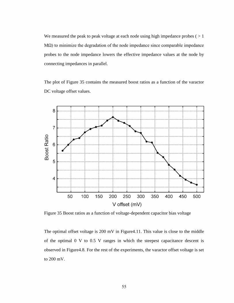
55
We measured the peak to peak voltage at each node using high impedance probes ( > 1
MΩ) to minimize the degradation of the node impedance since comparable impedance
probes to the node impedance lowers the effective impedance values at the node by
connecting impedances in parallel.
The plot of Figure 35 contains the measured boost ratios as a function of the varactor
DC voltage offset values.
Figure 35 Boost ratios as a function of voltage-dependent capacitor bias voltage
The optimal offset voltage is 200 mV in Figure4.11. This value is close to the middle
of the optimal 0 V to 0.5 V ranges in which the steepest capacitance descent is
observed in Figure4.8. For the rest of the experiments, the varactor offset voltage is set
to 200 mV.
56
4.2 Input amplitude sweep
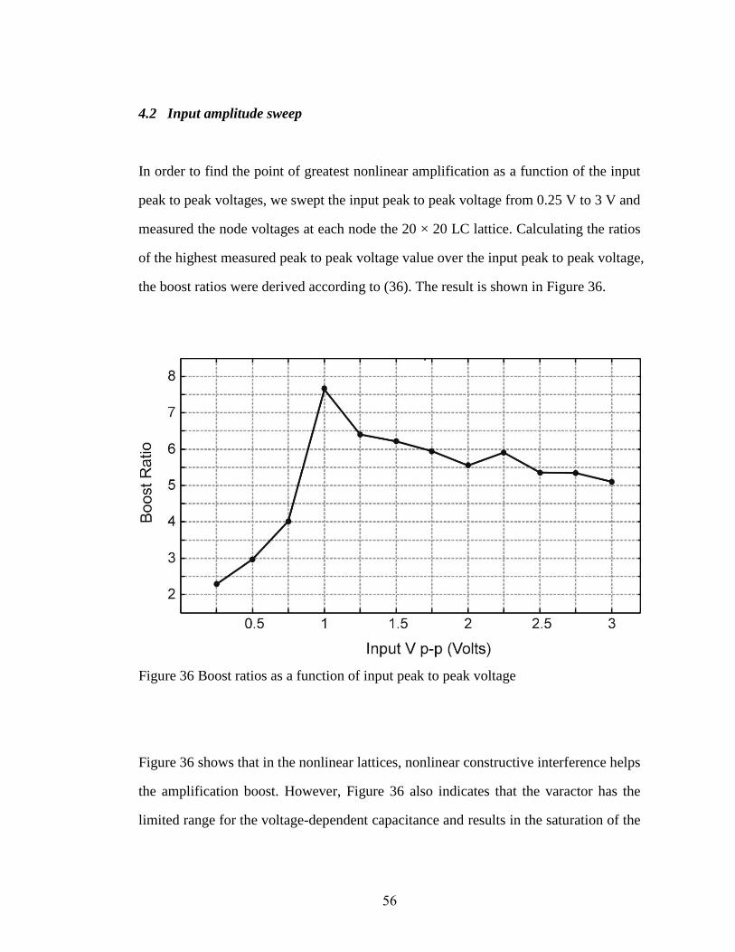
In order to find the point of greatest nonlinear amplification as a function of the input
peak to peak voltages, we swept the input peak to peak voltage from 0.25 V to 3 V and
measured the node voltages at each node the 20 × 20 LC lattice. Calculating the ratios
of the highest measured peak to peak voltage value over the input peak to peak voltage,
the boost ratios were derived according to (36). The result is shown in Figure 36.
Figure 36 Boost ratios as a function of input peak to peak voltage
Figure 36 shows that in the nonlinear lattices, nonlinear constructive interference helps
the amplification boost. However, Figure 36 also indicates that the varactor has the
limited range for the voltage-dependent capacitance and results in the saturation of the

57
boost ration in the nonlinear lattices. As seen the results, for the rest of the
experiments, the optimal 1 V peak to peak input amplitude was retained.
4.3 Frequency sweep
In order to verify the lattice modal analysis, we plotted the maximum measured peak
to peak voltage value as a function of the input frequency. Furthermore since the input
amplitude was kept constant a 1 V peak to peak, these observed maximum peak to
peak values are equal with the lattice boost ratios. These measurements are displayed
in Figure 37.
Figure 37 Boost ratios as a function of the input frequency

58
The experimental results of Figure 37 agree with the conclusions of the eigenvalue
analysis mentions in section 3.1. Nonlinear amplification appears in frequencies 8, 13,
18, 28 MHz with boost ratios greater than 5. Additionally, as the frequency increases,
and for frequencies higher than 30 MHz, the amplification becomes linear with boost
ratios < 4.5. This is expected since for fundamental frequencies higher than 30 MHz
the excited higher order harmonics exceed the cutoff frequency bound of 60 MHz
given L and C.
The amplification observed at frequency 13.5 MHz can be explained by comparing the
minima in Figure 33 and the harmonics of 13.5 MHz. The third harmonic (3 x 13.5 =
40.5 MHz) and the forth harmonic (4 x 13.5 = 54 MHz) are “near-by” fmode and fcutoff in
Figure 33 respectively. The effects of these excitations are added to the effects caused
by the fundamental and the second harmonic. In this way, the final amplification is
maximized.
Additionally, the amplification observed at frequency 28 MHz can be explained by the
excitation of the lattice at nearby fcutoff by the second harmonic (2 x 28 = 56 MHz)
which is added to the effect caused by the fundamental frequency. The effects
generated by the third (3 x 28 = 84 MHz) or higher harmonics are subsided by the 60
MHz cutoff frequency bound.
In the same way, the amplification observed at frequency 18.5 MHz can be explained
by the excitation of the lattice mode at nearby fcutoff by the third harmonic (3 x 18.5 =
55.5 MHz).
The cutoff frequency value calculated in section 3.1 agrees with the experimental
results of Figure 37 since after 61 MHz the boost ratio becomes smaller than 1. Based

59
on these results, the operating frequency for the rest of the experiments was chosen to
be 13.5 MHz.
4.4 Optimal results
Based on previous experimental measurements, the optimal conditions at which the
greatest nonlinear harmonic amplification is observed are:
Input peak to peak amplitude pp
inV = 1 V
Operating frequency inf = 13.5 MHz
Varactor bias voltage offV = 200 mV
In these conditions, the maximum voltage peak to peak value is obtained at the node
(9, 9). The waveform measured at node (9, 9) is compared to the input waveform at
node (1, 10). Both waveforms are displayed in the left plot of Figure 38. Their
respective Fourier transforms are displayed in the right plot of Figure 38, and the
results are shown in Table 8. In addition, Figure 39 is the result of MATLAB
simulation based on the optimal conditions
Table 8 Input and output pulse comparison
Input Output
Peak to Peak Amplitude 1 V 7.5 V
Pulse Width 74 ns 14 ns

60
Figure 38 Optimized output in time-domain response (Left) and frequency-domain
response (Right)
Figure 39 Nonlinear constructive interference in 2-D LC lattice. MATLAB simulation
61
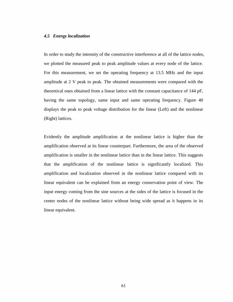
4.5 Energy localization
In order to study the intensity of the constructive interference at all of the lattice nodes,
we plotted the measured peak to peak amplitude values at every node of the lattice.
For this measurement, we set the operating frequency at 13.5 MHz and the input
amplitude at 2 V peak to peak. The obtained measurements were compared with the
theoretical ones obtained from a linear lattice with the constant capacitance of 144 pF,
having the same topology, same input and same operating frequency. Figure 40
displays the peak to peak voltage distribution for the linear (Left) and the nonlinear
(Right) lattices.
Evidently the amplitude amplification at the nonlinear lattice is higher than the
amplification observed at its linear counterpart. Furthermore, the area of the observed
amplification is smaller in the nonlinear lattice than in the linear lattice. This suggests
that the amplification of the nonlinear lattice is significantly localized. This
amplification and localization observed in the nonlinear lattice compared with its
linear equivalent can be explained from an energy conservation point of view. The
input energy coming from the sine sources at the sides of the lattice is focused in the
center nodes of the nonlinear lattice without being wide spread as it happens in its
linear equivalent.

62
Figure 40 Comparison of peak to peak voltage values between the linear (Left) and the
nonlinear (Right) lattices
The results observed in the nonlinear lattice are not symmetrical with respect to the i=j
diagonal nodes. This is caused by the non identical capacitance and inductance values
(based on the manufacture’s specifications tolerance)
5 Picosecond pulse generation on CMOS
To extend this idea to the higher frequency band, a nonlinear LC lattice is
implemented in TSMC 65 nm CMOS process [36]. The cutoff frequency of an active
device in this process, such as nMOS devices, is around 150 GHz and the maximum
operating frequency is around 180 GHz. However, as proposed in [29], this work
proved that using the nonlinearity without active devices could be a promising method
to bridge the terahertz gap. Figure 41 shows that the output waveform has strong

63
components even at 250 GHz which is beyond the cutoff frequency of the active
device in the same process.
Figure 41 Output response in IC with the high frequency input signal in time-domain
(Left) and frequency-domain (Right)
For varactors, an accumulation mode nMOS is used and coplanar-waveguide inductors
are used. It is noteworthy that in CMOS at higher frequencies, the quality factor of the
varactor drops very rapidly comparing to the quality factor of the inductor because of
the increase in the parasitic conductance. To alleviate this effect, the characteristic
impedance show be lowered compared to the characteristic impedance in the PCB.
Table 9 shows the boost ratio is 3.5 and picoseconds pulse generation with nonlinear
constructive harmonic interference in TSMC 65 nm CMOS process.
Table 9 Input and output pulse comparison
Input Output
Peak to Peak Amplitude 1 V 3.5 V
Pulse Width 20 ps 1.6 ps
64
6 Conclusions
We studied nonlinear LC lattices using theoretical and experimental tools and showed
that when nonlinear LC lattices operate at optimal conditions, they can generate high-
order harmonics with large amplitude. The harmonics can go up to several hundred
GHz beyond the cutoff frequency on a standard CMOS process. These optimal
conditions can be specified by applying a sequence of test such as varactor bias
voltage, input peak to peak amplitude, and input frequency. To provide more intuitive
analysis, we approached using both mathematical and numerical analysis.

65
REFERENCES
[1] Jansson,J.-P., Mantyniemi, A., Kostamovaara, J., “A CMOS time-to-ditigal
converter with better than 10 ps single-shot precision,” Solid-State Circuits, IEEE
Journal, vol.41, no.6, pp. 1286-1296, June 2006
[2] Steyaert, M., Peluso, V., Bastos, J., Kinget, P., Sansen, W., “Custom analog low
power design: The problem of low voltage and mismatch,” 1997 IEEE Custom
Integrated Circuits Conference, pp. 285-292, May 1997
[3] Bult, K., “Analog design in deep sub-micron CMOS,” Proceedings of the 26th
European Solid-State Circuits Conference, September 2000
[4] Staszewski, R.B, et al, “All-digital TX frequency synthesizer and discrete-time
receiver for Bluetooth radio in 130nm CMOS,” Solid-State Circuits, IEEE Journal,
vol.39, no.12, pp. 2278-2291, Dec. 2004
[5] H. Pan and A. Abidi, “Signal Folding in A/D Converters,” IEEE Trans. Circuits
Syst., vol. 51, pp. 3-14, Jan. 2004
[6] Y. Tousi, G. Li, A. Hassibi, and E. Afshari, “A 4-bit, 1mW Analog-to-Digital
Converter at 1GSample/sec,” Proc. of IEEE International Symposium on Circuits
and Systems, 2009
[7] T. Watanabe, T. Mizuno, and Y. Makino, “An All-Digital Analog-to-Digital
Converter With 12-μV/LSB Using Moving-Average Filtering,” IEEE J. of Solid-
state Circuits, vol. 38, pp. 120-125, January 2003
[8] M. Saint-Laurent and M. Swaminathan, “A digitally adjustable resistor for path
delay characterization in high frequency microprocessors,” in Proc. Southwest
Symp. Mixed-Signal Design, pp. 61–64, 2001

66
[9] M. G. Johnson, E. L. Hudson, and H. Kopka, “A variable delay line PLL for CPU-
Coprocessor synchronization,” IEEE J. Solid-State Circuits, vol. 23, pp. 1218-
1223, Oct. 1988
[10] T. Watanabe, Y. Makino, Y. Ohtsuka, S. Akita, and T. Hattori, “A CMOS time-
to-digital converter LSI with half-nanosecond resolution using a ring gate delay
line,” IEICE Trans. Electron., vol. E76-C, , pp. 1774-1779, Dec. 1993
[11] Farkhani, H., Meymandi-Nejad, M., Sachdev, M., “A fully digital ADC using a
new delay element with enhanced linearity,” IEEE International Symposium on
Circuits and Systems, pp. 2406-2409, May 2008
[12] D.Jeong et al., “Design of PLL-based clock generation circuits,” IEEE Journal of
Solid-State Circuits, vol. SC22, pp. 255-261, April 1987
[13] W. C. Black Jr., D. A. Hodges, “Time Interleaved Converter Arrays,” IEEE
Journal of Solid-State Circuits, vol. 15, pp. 1022-1029, December 1980
[14] Jan M. Rabaey, Digital Integrated Circuits,: A Design Perspective, New Jersey,
Prentice Hall, 2003
[15] T.Watanabe, Y. Makino, Y. Ohtsuka, S. Akita, and T. Hattori, “A CMOS time-to-
digital converter LSI with half-nanosecond resolution using a ring gate delay line,”
IEICE Trans. Electron., vol. E76-C, no. 12, pp. 1774–1779, Dec. 1993
[16] S. Yamauchi and T. Watanabe, “Ring oscillator and pulse phase difference
encoding circuit,” U.S. Patent 5416444, May 16, 1995
[17] K. Poulton et al., “A 20GS/s 8b ADC with a 1MB Memory in 0.18μm CMOS”,
ISSCC Dig. Tech. Papers, pp. 318-319, Feb., 2003
[18] B. Verburggen, J. Cranincks, M. Kuijk, P. Wambacq and G. V. Plas, “A 2.2mW
5b 1.75GS/s Folding Flash ADC in 90nm Digital CMOS,” ISSCC Dig. Tech.
Papers, pp. 252-253, Feb. 2008

67
[19] Y.-T. Wang and B. Razavi, “An 8-bit 150-MHz CMOS A/D converter,” IEEE J.
Solid-State Circuits, vol. 35, pp. 308–317, Mar. 2000
[20] M.-J. Choe, B.-S. Song, and K. Bacrania, “An 8-b 100-MSample/s CMOS
pipelined folding ADC,” IEEE J. Solid-State Circuits, vol. 36, pp. 184–194, Feb.
2001
[21] K. Yoon, J. Lee, D.-K. Jeong, and W. Kim, “An 8-bit 125 MS/s CMOS folding
ADC for Gigabit Ethernet LSI,” in Proc. VLSI Circuits Symp., pp. 212–213, 2000
[22] R. C. Taft and M. R. Tursi, “A 100-MS/s 8-b CMOS subranging ADC with
sustained parametric performance from 3.8 V down to 2.2 V,” IEEE J. Solid-State
Circuits, vol. 36, pp. 331–338, Mar. 2001
[23] S. Limotyrakis, S. D. Kulchycki, D. Su, and B. A.Wooley, “A 150 MS/s 8 b 71
mW time-interleaved ADC in 0.18 _m CMOS,” in ISSCC Dig. Tech. Papers, pp.
258–259, 2004
[24] Mulder, J., et al, “A 21-mW 8-b 125 MSample/s ADC in 0.09-mm2 0.13-µm
CMOS,” IEEE Journal of Solid-State Circuits, vol. 39, no. 12, pp. 2116-2125, Dec.
2004
[25] P. H. Seigel, “Terahertz Technology,” IEEE Trans. Microwave Theory Tech., vol.
50, no. 3, pp. 910-928, Mar. 2002
[26] D. W. Van der Weide, J. Murakowski, F. Keilmann, “Gas-absorption
spectroscopy with Electronic Terahertz Techniques,” IEEE Trans. Microwave
Theory Tech., vol. 48, no. 4, pp. 740-743, Apr. 2000
[27] R.Piesiewicz, T. K. Ostmann, N. Krumbholz, D. Mittleman, M. Koch, J.
Schoebel, T. Kurner, ”Short-Range Ultra-Broadband Terahertz Communications:
Concepts and Perspectives, IEEE Antennas Propag. Mag. Vol. 49, No. 6, pp. 24-
39, Dec. 2007
68
[28] Z. Jiang, X. Zhang, ”Terahertz Imaging via Electrooptic Effect”, IEEE Trans.
Microwave Theory Tech., Vol. 47, No. 12, pp. 2644-2650, Dec. 1999
[29] T. W. Crow, et al., “Opening the Terahertz Window with Integrated Diode
Circuits,” IEEE J. Solid-Stat Circuits, vol. 40, no. 10, pp. 2104-2110, Oct. 2005
[30] E. Afshari and A. Hajimiri, ”A Non-Linear Transmission Lines for Pulse Shaping
in Silicon”, IEEE Journal of Solid-State Circuits, Vol. 40, No. 3, pp. 744-52, Mar.
2005
[31] H. S. Bhat, E. Afshari, ”Nonlinear constructive interference in electrical lattices”,
Phys. Rev. E, Vol. 77, No. 6, pp. 066602 1-13, June 2008
[32] O. C. Zienkiewicz: “The Finite Element Method”, Mc Graw Hill, 1989
[33] S. Barbieri et al., “Continuous-wave operation of terahertz quantum cascade
lasers,” IEEE J. Quantum Electron., vol. 39, no. 4, pp. 586–591, Apr. 2003
[34] B. S. Williams, S. Kumar, H. Callebaut, Q. Hu, and J. L. Reno, “3.4 THz
quantum cascade laser operating above liquid nitrogen temperature,” Electron.
Lett., vol. 39, no. 12, pp. 915–916, Jun. 12, 2003
[35] G. Lilis, H. S. Bhat, J. Park, and E. Afshari, “Observation of nonlinear wave
synthesis in an inductor-capacitor lattice,” to appear in Physical Review Letters,
2009
[36] W. Lee, F. Amoozegar, and E. Afshari, “Picosecond Pulse Generation on CMOS:
Design Beyond Transistor Limits,” Proc. of IEEE Radar Conference, 2009
[37] R. Landauer, “Parametric Amplification Along Nonlinear Transmission Lines,”
Journal of Applied Physics, vol. 31, pp. 479-484, 1960
[38] R. Hirota and K. Suzuki,“Studies on Lattice Solitons by Using Electrical
Networks,” Journal of Physical Society of Japan, vol. 28, 1366, 1970

69
[39] H. Ikezi, S. S. Wojtowicz, R. E. Waltz, and D. R. Baker, “Temporal Contraction
of Solitons in a Nonuniform Transmission-Line,” Journal of Applied Physics, vol.
64, 6836, 1988
[40] M. J. W. Rodwell, et al.,“Active and Nonlinear-Wave Propagation Devices in
Ultrafast Electronics and Optoelectronics,” Proceedings of the IEEE, vol. 82, pp.
1037-1059, 1994
[41] E. Afshari, H. S. Bhat, A. Hajimiri, and J. E. Marsden, “Extremely Wideband
Signal Shaping Using One-and Two-Dimensional Nonuniform Nonlinear
Transmission Lines,” Journal of Applied Physics, vol. 99, 2006